EP3905520A1 - Bulk acoustic wave resonator having asymmetric electrode thickness, filter, and electronic device - Google Patents
Bulk acoustic wave resonator having asymmetric electrode thickness, filter, and electronic device Download PDFInfo
- Publication number
- EP3905520A1 EP3905520A1 EP19902251.8A EP19902251A EP3905520A1 EP 3905520 A1 EP3905520 A1 EP 3905520A1 EP 19902251 A EP19902251 A EP 19902251A EP 3905520 A1 EP3905520 A1 EP 3905520A1
- Authority
- EP
- European Patent Office
- Prior art keywords
- thickness
- resonator according
- electrode
- resonator
- range
- Prior art date
- Legal status (The legal status is an assumption and is not a legal conclusion. Google has not performed a legal analysis and makes no representation as to the accuracy of the status listed.)
- Pending
Links
Images



Classifications
-
- H—ELECTRICITY
- H03—ELECTRONIC CIRCUITRY
- H03H—IMPEDANCE NETWORKS, e.g. RESONANT CIRCUITS; RESONATORS
- H03H9/00—Networks comprising electromechanical or electro-acoustic elements; Electromechanical resonators
- H03H9/02—Details
- H03H9/02007—Details of bulk acoustic wave devices
- H03H9/02086—Means for compensation or elimination of undesirable effects
- H03H9/02118—Means for compensation or elimination of undesirable effects of lateral leakage between adjacent resonators
-
- H—ELECTRICITY
- H03—ELECTRONIC CIRCUITRY
- H03H—IMPEDANCE NETWORKS, e.g. RESONANT CIRCUITS; RESONATORS
- H03H9/00—Networks comprising electromechanical or electro-acoustic elements; Electromechanical resonators
- H03H9/02—Details
- H03H9/02007—Details of bulk acoustic wave devices
- H03H9/02157—Dimensional parameters, e.g. ratio between two dimension parameters, length, width or thickness
-
- H—ELECTRICITY
- H03—ELECTRONIC CIRCUITRY
- H03H—IMPEDANCE NETWORKS, e.g. RESONANT CIRCUITS; RESONATORS
- H03H9/00—Networks comprising electromechanical or electro-acoustic elements; Electromechanical resonators
- H03H9/02—Details
- H03H9/125—Driving means, e.g. electrodes, coils
- H03H9/13—Driving means, e.g. electrodes, coils for networks consisting of piezoelectric or electrostrictive materials
- H03H9/131—Driving means, e.g. electrodes, coils for networks consisting of piezoelectric or electrostrictive materials consisting of a multilayered structure
-
- H—ELECTRICITY
- H03—ELECTRONIC CIRCUITRY
- H03H—IMPEDANCE NETWORKS, e.g. RESONANT CIRCUITS; RESONATORS
- H03H9/00—Networks comprising electromechanical or electro-acoustic elements; Electromechanical resonators
- H03H9/02—Details
- H03H9/125—Driving means, e.g. electrodes, coils
- H03H9/13—Driving means, e.g. electrodes, coils for networks consisting of piezoelectric or electrostrictive materials
- H03H9/132—Driving means, e.g. electrodes, coils for networks consisting of piezoelectric or electrostrictive materials characterized by a particular shape
Definitions
- Embodiments of the present disclosure relate to the field of semiconductors, in particular to a bulk acoustic resonator, a filter having the resonator, and electronic equipment having the resonator or the filter.
- a film bulk acoustic resonator made by the longitudinal resonance of a piezoelectric film in the thickness direction has become a feasible alternative to surface acoustic wave devices and quartz crystal resonators in terms of mobile phone communication and highspeed serial data applications.
- a radio frequency front end bulk wave filter/duplexer provides superior filtering characteristics, such as low insertion loss, steep transition band, higher power capacity, and stronger electrostatic discharge (ESD) resistance.
- ESD electrostatic discharge
- a high-frequency film bulk acoustic resonator with ultra-low frequency temperature drift has low phase noise, low power consumption and a large bandwidth modulation range.
- these miniature film resonators use CMOS-compatible processing technology on silicon substrates, which can reduce the unit cost and facilitate the final integration with CMOS circuits.
- the bulk acoustic resonator structure shown in Fig. 1a and Fig. 1b specifically has a substrate P100; an acoustic mirror P200 is embedded into the substrate or is located on the surface of the substrate, the specific form of the acoustic mirror P200 may include a cavity or a Bragg reflecting layer or other equivalent structures capable of reflecting acoustic waves; a bottom electrode P300 covers the acoustic mirror structure and a part of the substrate; a piezoelectric film layer P400 covers the bottom electrode and a part of the substrate; and a top electrode P500 is located on the piezoelectric layer and covers a part of the piezoelectric layer, wherein the lateral overlapping part of the top electrode P500, the piezoelectric layer P400, the bottom electrode P300 and the cavity P200 defines an effective acoustic region AR of the bulk acoustic resonator.
- the bottom electrode BE and the top electrode TE further have electrode pins P301 and P501 as shown in Fig
- An enhancement structure P600 is further arranged on the surface of the top electrode or the bottom electrode (P600 in Fig. 1b is only a schematic diagram and does not represent a precise structure), the enhancement structure may include a protrusion structure for reflecting acoustic waves laterally propagating to the boundary of the effective region, thereby improving the Q value of the resonator.
- adjustment process layers that usually cover the surfaces of the functional layers such as P500 and P400 of the resonator are omitted.
- This type of process layers usually protects the resonator from the erosion of external water vapor and oxygen, or adjusts the performance parameters (such as frequency) of the resonator.
- the enhancement structure can be arranged to reflect the laterally propagating acoustic waves to improve the Q value, in reality, there is a need to further strengthen the acoustic wave reflection function.
- a bulk acoustic resonator including: a substrate; an acoustic mirror; a sandwich structure comprising a top electrode, a piezoelectric layer and a bottom electrode, wherein the overlapping parts of the top electrode, the piezoelectric layer and the bottom electrode with the acoustic mirror in the thickness direction of the resonator form an effective region; and an enhancement structure arranged on one side of the sandwich structure, wherein: the thickness of the electrode located on the one side of the sandwich structure is smaller than the thickness of the electrode located on the other side of the sandwich structure.
- the ratio of the thickness of the electrode located on the other side of the sandwich structure to the thickness of the electrode located on one side of the sandwich structure is in the range of 1.1-2.5. Further, the ratio of the thickness of the electrode located on the other side of the sandwich structure to the thickness of the electrode located on one side of the sandwich structure is in the range of 1.5-2.25.
- the embodiments of the present disclosure further relate to a filter, including the above-mentioned bulk acoustic resonator.
- the embodiments of the present disclosure further relate to electronic equipment, including the above-mentioned bulk acoustic resonator or the above-mentioned filter.
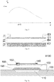
- Fig. 2 is a schematic diagram of a top electrode and a bottom electrode of a sandwich structure of the resonator in the prior art with equal thickness; and Fig. 4 is a schematic diagram of a sandwich structure of a resonator according to an exemplary embodiment of the present disclosure.
- the sandwich structure includes a top electrode E1, a piezoelectric layer E4, a bottom electrode E2, and an enhancement structure E3 arranged at the end part of the top electrode E1.
- the enhancement structure is used for reflecting acoustic waves laterally propagating to the boundary of an effective region, thereby improving the Q value of the resonator.
- Fig. 4 The difference between Fig. 4 and Fig. 2 lies in that the thickness of the top electrode E1 becomes smaller, while the thickness of the bottom electrode E2 becomes greater. It can also be seen from Fig. 4 that the enhancement structure E3 is arranged on the side of the electrode with the reduced thickness.
- the thickness T1+T2+T0 of the sandwich structure in Fig. 2 is the same as the thickness T1+T2+T0 of the sandwich structure in Fig. 4 .
- Fig. 3 is a diagram showing the relationship between electromechanical coupling coefficient (kt 2 ) of the sandwich structure of the resonator and the thickness ratio r of the two electrodes in the prior art.
- Fig. 3 is a diagram showing the experiment and simulation results of the inventor. If other conditions remain unchanged, when the thicknesses of the top electrode and the bottom electrode are the same (that is, when the thickness ratio r of the electrodes is 1), the sandwich structure has the maximal electromechanical coupling coefficient (kt 2 max), and the electromechanical coupling coefficient will be reduced by the electrodes with unequal thicknesses.
- Fig. 5a is a schematic diagram of a resonator according to an exemplary embodiment A100 of the present disclosure
- Fig. 5b is an enlarged schematic diagram of the enhancement structure used in Fig. 5a .
- the resonator structure in the embodiment A100 includes: a substrate 100, an acoustic mirror (cavity) 110, a bottom electrode 120, a piezoelectric layer 130, a top electrode 140, and an enhancement structure 150 located at the edge of the top electrode.
- the surface of the resonator may also be covered with other process layers 160 according to specific needs, such as passivation layers for preventing water vapor and inhibiting oxidation (the process layers are also applicable to subsequent embodiments and will not be shown in subsequent figures).
- the thickness of the bottom electrode is greater than the thickness of the top electrode, and the thickness ratio of the bottom electrode to the top electrode is in the range of 1.1-2.5, and the further range is 1.5-2.25. It should be pointed out that this requirement includes the case where the process layer 160 is taken into consideration. Subsequent embodiments are similarly processed, that is, when the process layer is provided, the thickness ratio of the electrode on the side with no thickness reduction to the electrode on the side with thickness reduction still meets the above-mention proportional range when the thickness of the process layer is included.
- the ratio of the thickness of the electrode located on the other side of the sandwich structure to the thickness of the electrode located on one side of the sandwich structure may be 1.1, 1.3, 2.0, 2.25, 2.5, etc.
- the bottom electrode 120 may be made of a single-layer metal material or an alloy, or a multilayer composite material.
- the metal materials adopted by the top electrode and the bottom electrode may be the same or different.
- the enhancement structure 150 in Fig. 5a is only schematic and does not represent a specific structure, which is also the same in the subsequent embodiments.
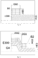
- An enhancement structure shown in Fig. 5b includes a blocky protrusion B0 located on the electrode E099, wherein the material of the blocky protrusion B0 may be the same as or different from that of the electrode E099.
- the thickness of the blocky protrusion B0 is HB0
- the width of the blocky protrusion B0 is DB0
- the thickness of the electrode E099 is HE0.
- the width DB0 of the blocky protrusion B0 is in the range of 0.5 microns to 7 microns, for example, 0.5 microns, 1 micron, 2 microns, 5 microns, 7 microns, or the like; and optionally, DB0 is in the range of 0.5 microns to 2 microns, and it can also be 1/4 of the wavelength ⁇ of the transverse lamb wave in the S1 mode, or an odd multiple of 1/4 of the wavelength ⁇ of the lamb wave.
- the S1 mode will be described below with reference to Fig. 10 .
- Fig. 10 when the bulk acoustic resonator is working, a large number of vibrations are generated in the sandwich structure, if these vibrations are plotted as a dispersion curve according to the relationship between the frequency (f) and the wave number (k), the curves of a variety modes can be obtained, the curve of one mode is called the S1 mode (the curves of the other modes are not shown in Fig. 10 ), which has a dispersion curve of the shape shown in Fig. 10 , wherein the abscissa represents the wave number and the vertical coordinate represents the vibration frequency.
- the vibration frequency is parallel resonance frequency f p
- the corresponding wave number is k p
- the thickness HE0 of the blocky protrusion B0 is in the range of 500-2500 ⁇ , for example, may be 500 ⁇ , 800 ⁇ , 1400 ⁇ , 2500 ⁇ , and the like.
- the electrode E300 of an airfoil structure has a protruding part, and the protruding part is defined as the part in a dotted line region B2, the width of the protruding part is defined as DG3, the width of the airfoil part is defined as AW2, and the thickness of the protruding dpart is defined as HG3.
- the thickness of the electrode E300 is HE3, and there is a gap G4 below the airfoil structure.
- the specific enhancement structure 150 is not limited to the form shown in Figs. 5b-5c , and may also be any other enhancement structures easily conceived by those skilled in the art.
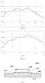
- Fig. 9 is an exemplary relationship diagram of an exemplary embodiment of the parallel resonance impedance of the resonator and the width of the enhancement structure, wherein the vertical axis represents the parallel resonance impedance of the resonator, the horizontal axis represents the width of the enhancement structure, the broken line with a triangle shows the parallel resonance impedance after the thickness of the electrode is reduced (that is, the thicknesses of the top electrode and the bottom electrode are different), and the broken line with a circle shows the parallel resonance impedance with the thickness ratio of the electrodes is 1.
- the abscissa represents the ratio of the thickness of the electrode on the non-enhancement structure side to the thickness of the electrode on the enhancement structure side, and the vertical coordinate represents the parallel resonance impedance.
- the abscissa represents the ratio of the thickness of the electrode on the non-enhancement structure side to the thickness of the electrode on the enhancement structure side, and the vertical coordinate represents the parallel resonance impedance.
- Fig. 5d and Fig. 5e exemplarily show changing curves of the parallel resonance impedance when the width of the enhancement structure is constant and the thickness ratios of the electrodes are different.
- Fig. 6 is a schematic diagram of a resonator according to another exemplary embodiment A200 of the present disclosure.
- the thickness of the bottom electrode is greater than that of the top electrode.
- the difference between the embodiment A200 and the embodiment A100 lies in that the enhancement structure in the embodiment A200 is located on the lower surface of the top electrode.
- the enhancement structure is a protrusion embedded into the piezoelectric layer 230.
- the enhancement structure may also be a cavity (which can be filled with a solid material or not) arranged on the upper surface of the piezoelectric layer 230 or the lower surface or the upper surface of the top electrode 240, and may also be a combination of a protrusion and a cavity or other forms.
- Fig. 7 is a schematic diagram of a resonator according to yet another exemplary embodiment A300 of the present disclosure.
- the difference between the embodiment A300 and the embodiments A100 and A200 lies in that: in the embodiment A300, the thickness of the bottom electrode is relatively small, and the enhancement structure is located on the upper surface of the bottom electrode.
- the enhancement structure is a protrusion embedded into the piezoelectric layer 330.
- Fig. 8 is a schematic diagram of a resonator according to still another exemplary embodiment A400 of the present disclosure.
- the thickness of the bottom electrode is relatively small, and the enhancement structure is located on the lower surface of the bottom electrode.
- the enhancement structure is a protrusion protruding into the cavity or a reflector 410.
- the enhancement structure is arranged on the top electrode, the bottom electrode or the piezoelectric layer, for different reflector structures, the enhancement structure may also be arranged at other positions in the resonator.
- the reflection performance of the enhancement structure for the laterally propagating acoustic waves can be effectively improved.
- the reflection performance is mainly reflected in the improvement effect of the asymmetric structure on the parallel resonance impedance of the resonator, and for the bulk acoustic resonator, the greater the parallel resonance impedance is, the better the performance is.
- the present disclosure further proposes doping the piezoelectric layer to compensate the loss of the electromechanical coupling coefficient caused thereby.
- Fig. 11 shows a schematic diagram of a resonator according to an exemplary embodiment A500 of the present disclosure, wherein a protruding enhancement structure and a recessed structure are shown.
- the acoustic wave reflection performance of the protruding enhancement structure can be improved, and the Q value of the resonator can be improved, but at the same time, clutter in a parasitic mode may also be enhanced.
- a "recessed" suppression structure i.e., the recessed structure
- the recessed structure can be added on the basis of the previous embodiment to suppress the acoustic waves in the above-mentioned parasitic mode.
- the depth value of the recessed structure may be the same as the thickness value of the protruding enhancement structure, and the width value of the recessed structure may be the same as the width value of the protruding enhancement structure.
- the recessed structure 155 is arranged on the inner side of the protruding enhancement structure and adjacent to the protruding enhancement structure.
- the material of the piezoelectric layer can be selected from, but is not limited to: aluminum nitride, wherein the doping element includes: scandium (preferably), yttrium, magnesium, titanium, or other rare earth elements.
- the doping atomic fraction ranges from 1% to 40%, and preferably ranges from 3% to 20%.
- the specific atomic fraction may be 1%, 3%, 6%, 20%, 30%, 40%, and so on.
- zinc oxide, lithium niobate, or lead zirconate titanate (PZT) may also be used as the main material of the piezoelectric layer and are doped with the above elements.
- the aforementioned piezoelectric material is a thin film with a thickness less than 10 microns, wherein the aluminum nitride thin film is in a polycrystalline form or a single crystal form, and the growth mode is thin film sputtering or metal-organic chemical vapor deposition (MOCVD).
- MOCVD metal-organic chemical vapor deposition
- the material of the substrate can be selected from, but is not limited to: single crystal silicon, quartz, gallium arsenide or sapphire, etc.
- the material of the electrode includes, but is not limited to: molybdenum, ruthenium, gold, magnesium, aluminum, tungsten, titanium, chromium, iridium, osmium, and the like, and multilayer composite materials or alloys of the above metals can also be used.
- the present disclosure further relates to a filter, including the above-mentioned resonator.
- the present disclosure further relates to electronic equipment, including the above-mentioned resonator or filter.
- electronic equipment includes, but is not limited to, intermediate products such as radio frequency front ends, filter amplifier modules, and terminal products such as mobile phones, WIFI and drones.
Landscapes
- Physics & Mathematics (AREA)
- Acoustics & Sound (AREA)
- Piezo-Electric Or Mechanical Vibrators, Or Delay Or Filter Circuits (AREA)
Abstract
Description
- Embodiments of the present disclosure relate to the field of semiconductors, in particular to a bulk acoustic resonator, a filter having the resonator, and electronic equipment having the resonator or the filter.
- A film bulk acoustic resonator made by the longitudinal resonance of a piezoelectric film in the thickness direction has become a feasible alternative to surface acoustic wave devices and quartz crystal resonators in terms of mobile phone communication and highspeed serial data applications. A radio frequency front end bulk wave filter/duplexer provides superior filtering characteristics, such as low insertion loss, steep transition band, higher power capacity, and stronger electrostatic discharge (ESD) resistance. A high-frequency film bulk acoustic resonator with ultra-low frequency temperature drift has low phase noise, low power consumption and a large bandwidth modulation range. In addition, these miniature film resonators use CMOS-compatible processing technology on silicon substrates, which can reduce the unit cost and facilitate the final integration with CMOS circuits.
- The bulk acoustic resonator structure shown in
Fig. 1a and Fig. 1b specifically has a substrate P100; an acoustic mirror P200 is embedded into the substrate or is located on the surface of the substrate, the specific form of the acoustic mirror P200 may include a cavity or a Bragg reflecting layer or other equivalent structures capable of reflecting acoustic waves; a bottom electrode P300 covers the acoustic mirror structure and a part of the substrate; a piezoelectric film layer P400 covers the bottom electrode and a part of the substrate; and a top electrode P500 is located on the piezoelectric layer and covers a part of the piezoelectric layer, wherein the lateral overlapping part of the top electrode P500, the piezoelectric layer P400, the bottom electrode P300 and the cavity P200 defines an effective acoustic region AR of the bulk acoustic resonator. Generally, the bottom electrode BE and the top electrode TE further have electrode pins P301 and P501 as shown inFig. 1a (not shown inFig. 1b ), respectively. - An enhancement structure P600 is further arranged on the surface of the top electrode or the bottom electrode (P600 in
Fig. 1b is only a schematic diagram and does not represent a precise structure), the enhancement structure may include a protrusion structure for reflecting acoustic waves laterally propagating to the boundary of the effective region, thereby improving the Q value of the resonator. - In addition, in
Fig. 1a and Fig. 1b , adjustment process layers that usually cover the surfaces of the functional layers such as P500 and P400 of the resonator are omitted. This type of process layers usually protects the resonator from the erosion of external water vapor and oxygen, or adjusts the performance parameters (such as frequency) of the resonator. - However, although the enhancement structure can be arranged to reflect the laterally propagating acoustic waves to improve the Q value, in reality, there is a need to further strengthen the acoustic wave reflection function.
- In order to alleviate or solve at least one aspect of the above-mentioned problems in the use of the prior art, the present disclosure is proposed.
- According to one aspect of the embodiments of the present disclosure, a bulk acoustic resonator is provided, including: a substrate; an acoustic mirror; a sandwich structure comprising a top electrode, a piezoelectric layer and a bottom electrode, wherein the overlapping parts of the top electrode, the piezoelectric layer and the bottom electrode with the acoustic mirror in the thickness direction of the resonator form an effective region; and an enhancement structure arranged on one side of the sandwich structure, wherein: the thickness of the electrode located on the one side of the sandwich structure is smaller than the thickness of the electrode located on the other side of the sandwich structure.
- Optionally, the ratio of the thickness of the electrode located on the other side of the sandwich structure to the thickness of the electrode located on one side of the sandwich structure is in the range of 1.1-2.5. Further, the ratio of the thickness of the electrode located on the other side of the sandwich structure to the thickness of the electrode located on one side of the sandwich structure is in the range of 1.5-2.25.
- The embodiments of the present disclosure further relate to a filter, including the above-mentioned bulk acoustic resonator.
- The embodiments of the present disclosure further relate to electronic equipment, including the above-mentioned bulk acoustic resonator or the above-mentioned filter.
- The following description and the drawings can better help understand these and other features and advantages in various embodiments disclosed in the present disclosure. The same reference signs in the figures always denote the same components, wherein:
-
Fig. 1a is a schematic top view of a bulk acoustic resonator in the prior art; -
Fig. 1b is a schematic cross-sectional view taken along a line AOA' inFig. 1a ; -
Fig. 2 is a schematic diagram of a top electrode and a bottom electrode of a sandwich structure of the resonator in the prior art with equal thickness; -
Fig. 3 is a diagram showing the relationship between an electromechanical coupling coefficient of the sandwich structure of the resonator and the thickness ratio of the two electrodes in the prior art; -
Fig. 4 is a schematic diagram of a sandwich structure of a resonator according to an exemplary embodiment of the present disclosure; -
Fig. 5a is a schematic diagram of a resonator according to an exemplary embodiment of the present disclosure; -
Fig. 5b is an exemplary schematic diagram of an enhancement structure; -
Fig. 5c is an optional exemplary schematic diagram of the enhancement structure; -
Fig. 5d is a schematic diagram of a simulation result based on the enhancement structure inFig. 5c ; -
Fig. 5e is a schematic diagram of a simulation result based on the enhancement structure inFig. 5c ; -
Fig. 6 is a schematic diagram of a resonator according to an exemplary embodiment of the present disclosure; -
Fig. 7 is a schematic diagram of a resonator according to an exemplary embodiment of the present disclosure; -
Fig. 8 is a schematic diagram of a resonator according to an exemplary embodiment of the present disclosure; -
Fig. 9 is an exemplary schematic diagram showing the relationship between the parallel resonance impedance of the resonator and the width of the enhancement structure; -
Fig. 10 shows a dispersion curve of an S1 mode; and -
Fig. 11 is a schematic diagram of a resonator according to an exemplary embodiment of the present disclosure, which shows a protruding enhancement structure and a recessed structure. - The technical solutions of the present disclosure will be further described below in detail through embodiments and in conjunction with the drawings. In the specification, the same or similar reference signs indicate the same or similar components. The following description of the embodiments of the present disclosure with reference to the drawings is intended to explain the general inventive concept of the present disclosure, and should not be construed as a limitation to the present disclosure.
- The present disclosure will be exemplarily described below with reference to the drawings.
-
Fig. 2 is a schematic diagram of a top electrode and a bottom electrode of a sandwich structure of the resonator in the prior art with equal thickness; andFig. 4 is a schematic diagram of a sandwich structure of a resonator according to an exemplary embodiment of the present disclosure. - As shown in
Fig. 2 andFig. 4 , the sandwich structure includes a top electrode E1, a piezoelectric layer E4, a bottom electrode E2, and an enhancement structure E3 arranged at the end part of the top electrode E1. The enhancement structure is used for reflecting acoustic waves laterally propagating to the boundary of an effective region, thereby improving the Q value of the resonator. - The difference between
Fig. 4 andFig. 2 lies in that the thickness of the top electrode E1 becomes smaller, while the thickness of the bottom electrode E2 becomes greater. It can also be seen fromFig. 4 that the enhancement structure E3 is arranged on the side of the electrode with the reduced thickness. - If it is necessary to keep the frequency of the resonator shown in
Fig. 2 unchanged inFig. 4 , it is also required that the thickness T1+T2+T0 of the sandwich structure inFig. 2 is the same as the thickness T1+T2+T0 of the sandwich structure inFig. 4 . -
Fig. 3 is a diagram showing the relationship between electromechanical coupling coefficient (kt2) of the sandwich structure of the resonator and the thickness ratio r of the two electrodes in the prior art.Fig. 3 is a diagram showing the experiment and simulation results of the inventor. If other conditions remain unchanged, when the thicknesses of the top electrode and the bottom electrode are the same (that is, when the thickness ratio r of the electrodes is 1), the sandwich structure has the maximal electromechanical coupling coefficient (kt2max), and the electromechanical coupling coefficient will be reduced by the electrodes with unequal thicknesses. -
Fig. 5a is a schematic diagram of a resonator according to an exemplary embodiment A100 of the present disclosure; andFig. 5b is an enlarged schematic diagram of the enhancement structure used inFig. 5a . - The resonator structure in the embodiment A100 includes: a
substrate 100, an acoustic mirror (cavity) 110, abottom electrode 120, apiezoelectric layer 130, atop electrode 140, and anenhancement structure 150 located at the edge of the top electrode. - Optionally, the surface of the resonator may also be covered with other process layers 160 according to specific needs, such as passivation layers for preventing water vapor and inhibiting oxidation (the process layers are also applicable to subsequent embodiments and will not be shown in subsequent figures).
- In the embodiment A100 , the thickness of the bottom electrode is greater than the thickness of the top electrode, and the thickness ratio of the bottom electrode to the top electrode is in the range of 1.1-2.5, and the further range is 1.5-2.25. It should be pointed out that this requirement includes the case where the
process layer 160 is taken into consideration. Subsequent embodiments are similarly processed, that is, when the process layer is provided, the thickness ratio of the electrode on the side with no thickness reduction to the electrode on the side with thickness reduction still meets the above-mention proportional range when the thickness of the process layer is included. The ratio of the thickness of the electrode located on the other side of the sandwich structure to the thickness of the electrode located on one side of the sandwich structure may be 1.1, 1.3, 2.0, 2.25, 2.5, etc. - The
bottom electrode 120 may be made of a single-layer metal material or an alloy, or a multilayer composite material. - When the top electrode and the bottom electrode are both made of a single-layer material, the metal materials adopted by the top electrode and the bottom electrode may be the same or different.
- The
enhancement structure 150 inFig. 5a is only schematic and does not represent a specific structure, which is also the same in the subsequent embodiments. - An enhancement structure shown in
Fig. 5b includes a blocky protrusion B0 located on the electrode E099, wherein the material of the blocky protrusion B0 may be the same as or different from that of the electrode E099. InFig. 5b , the thickness of the blocky protrusion B0 is HB0, the width of the blocky protrusion B0 is DB0, and the thickness of the electrode E099 is HE0. In an optional embodiment, the width DB0 of the blocky protrusion B0 is in the range of 0.5 microns to 7 microns, for example, 0.5 microns, 1 micron, 2 microns, 5 microns, 7 microns, or the like; and optionally, DB0 is in the range of 0.5 microns to 2 microns, and it can also be 1/4 of the wavelength λ of the transverse lamb wave in the S1 mode, or an odd multiple of 1/4 of the wavelength λ of the lamb wave. - The S1 mode will be described below with reference to
Fig. 10 . As shown inFig. 10 , when the bulk acoustic resonator is working, a large number of vibrations are generated in the sandwich structure, if these vibrations are plotted as a dispersion curve according to the relationship between the frequency (f) and the wave number (k), the curves of a variety modes can be obtained, the curve of one mode is called the S1 mode (the curves of the other modes are not shown inFig. 10 ), which has a dispersion curve of the shape shown inFig. 10 , wherein the abscissa represents the wave number and the vertical coordinate represents the vibration frequency. When the vibration frequency is parallel resonance frequency fp , the corresponding wave number is kp , and the wavelength λ of the S1 mode is defined as the following formula:
- In an optional embodiment, the thickness HE0 of the blocky protrusion B0 is in the range of 500-2500 Å, for example, may be 500 Å, 800 Å, 1400 Å, 2500 Å, and the like.
- As shown in
Fig. 5c , the electrode E300 of an airfoil structure has a protruding part, and the protruding part is defined as the part in a dotted line region B2, the width of the protruding part is defined as DG3, the width of the airfoil part is defined as AW2, and the thickness of the protruding dpart is defined as HG3. The thickness of the electrode E300 is HE3, and there is a gap G4 below the airfoil structure. Thespecific enhancement structure 150 is not limited to the form shown inFigs. 5b-5c , and may also be any other enhancement structures easily conceived by those skilled in the art. -
Fig. 9 is an exemplary relationship diagram of an exemplary embodiment of the parallel resonance impedance of the resonator and the width of the enhancement structure, wherein the vertical axis represents the parallel resonance impedance of the resonator, the horizontal axis represents the width of the enhancement structure, the broken line with a triangle shows the parallel resonance impedance after the thickness of the electrode is reduced (that is, the thicknesses of the top electrode and the bottom electrode are different), and the broken line with a circle shows the parallel resonance impedance with the thickness ratio of the electrodes is 1. - From the relationship diagram between the parallel resonant impedance and the width of the enhancement structure in
Fig. 9 , it can be seen that the parallel resonant impedance with an asymmetric structure (that is, the two electrodes have different thicknesses) is significantly higher than (the two curves only overlap within a small range) that in the case of an symmetrical structure (that is, the two electrodes have the same thickness) within the changing range of the width of the enhancement structure shown in the figure. As shown inFig. 9 , when the width of the enhancement structure is in the range of 0.5 microns to 1.25 microns, or not less than 1.5 microns, the parallel resonance impedance is greatly improved compared with the symmetrical arrangement structure with the same electrode thickness.Fig. 5d is a first simulation result diagram of the enhancement structure inFig. 5c , wherein the simulation conditions are set as HG3=600Å; DG3=1 µm, and AW2=1 µm. The abscissa represents the ratio of the thickness of the electrode on the non-enhancement structure side to the thickness of the electrode on the enhancement structure side, and the vertical coordinate represents the parallel resonance impedance. -
Fig. 5e is a second simulation result diagram of the enhancement structure inFig. 5c , wherein the simulation conditions are set as HG3=1200Å; DG3=1µm, and AW2=1µm. The abscissa represents the ratio of the thickness of the electrode on the non-enhancement structure side to the thickness of the electrode on the enhancement structure side, and the vertical coordinate represents the parallel resonance impedance. -
Fig. 5d and Fig. 5e exemplarily show changing curves of the parallel resonance impedance when the width of the enhancement structure is constant and the thickness ratios of the electrodes are different. - Based on
Fig. 5d and Fig. 5e , it can be seen that only when the thickness of the enhancement structure changes from 600 Å to 1200 Å, the change trends of the curves are roughly the same. - The above exemplary description of the enhancement structure is also applicable to other embodiments of the present disclosure.
-
Fig. 6 is a schematic diagram of a resonator according to another exemplary embodiment A200 of the present disclosure. InFig. 6 , the thickness of the bottom electrode is greater than that of the top electrode. The difference between the embodiment A200 and the embodiment A100 lies in that the enhancement structure in the embodiment A200 is located on the lower surface of the top electrode. As shown inFig. 6 , the enhancement structure is a protrusion embedded into thepiezoelectric layer 230. The enhancement structure may also be a cavity (which can be filled with a solid material or not) arranged on the upper surface of thepiezoelectric layer 230 or the lower surface or the upper surface of thetop electrode 240, and may also be a combination of a protrusion and a cavity or other forms. -
Fig. 7 is a schematic diagram of a resonator according to yet another exemplary embodiment A300 of the present disclosure. The difference between the embodiment A300 and the embodiments A100 and A200 lies in that: in the embodiment A300, the thickness of the bottom electrode is relatively small, and the enhancement structure is located on the upper surface of the bottom electrode. As shown inFig. 7 , the enhancement structure is a protrusion embedded into thepiezoelectric layer 330. -
Fig. 8 is a schematic diagram of a resonator according to still another exemplary embodiment A400 of the present disclosure. In the embodiment A400, the thickness of the bottom electrode is relatively small, and the enhancement structure is located on the lower surface of the bottom electrode. As shown inFig. 8 , the enhancement structure is a protrusion protruding into the cavity or areflector 410. - Although in the present disclosure, the enhancement structure is arranged on the top electrode, the bottom electrode or the piezoelectric layer, for different reflector structures, the enhancement structure may also be arranged at other positions in the resonator.
- In the present disclosure, if the thickness of the electrode on one side with the enhancement structure is decreased, and the thickness of the electrode on the other side is increased at the same time, the reflection performance of the enhancement structure for the laterally propagating acoustic waves can be effectively improved. The reflection performance is mainly reflected in the improvement effect of the asymmetric structure on the parallel resonance impedance of the resonator, and for the bulk acoustic resonator, the greater the parallel resonance impedance is, the better the performance is.
- Based on
Fig. 3 , it can be seen that the electromechanical coupling coefficient of the resonator will be reduced in the solution in which the thicknesses of the two electrodes are different. In order to keep the electromechanical coupling coefficient unchanged, the present disclosure further proposes doping the piezoelectric layer to compensate the loss of the electromechanical coupling coefficient caused thereby. -
Fig. 11 shows a schematic diagram of a resonator according to an exemplary embodiment A500 of the present disclosure, wherein a protruding enhancement structure and a recessed structure are shown. - Based on the asymmetric structure of the electrode thicknesses, the acoustic wave reflection performance of the protruding enhancement structure can be improved, and the Q value of the resonator can be improved, but at the same time, clutter in a parasitic mode may also be enhanced. In order to overcome the above-mentioned problem, a "recessed" suppression structure (i.e., the recessed structure) can be added on the basis of the previous embodiment to suppress the acoustic waves in the above-mentioned parasitic mode.
- The depth value of the recessed structure may be the same as the thickness value of the protruding enhancement structure, and the width value of the recessed structure may be the same as the width value of the protruding enhancement structure.
- As shown in
Fig. 11 , the recessedstructure 155 is arranged on the inner side of the protruding enhancement structure and adjacent to the protruding enhancement structure. - Correspondingly, the material of the piezoelectric layer can be selected from, but is not limited to: aluminum nitride, wherein the doping element includes: scandium (preferably), yttrium, magnesium, titanium, or other rare earth elements. The doping atomic fraction ranges from 1% to 40%, and preferably ranges from 3% to 20%. The specific atomic fraction may be 1%, 3%, 6%, 20%, 30%, 40%, and so on. In addition, zinc oxide, lithium niobate, or lead zirconate titanate (PZT) may also be used as the main material of the piezoelectric layer and are doped with the above elements. The aforementioned piezoelectric material is a thin film with a thickness less than 10 microns, wherein the aluminum nitride thin film is in a polycrystalline form or a single crystal form, and the growth mode is thin film sputtering or metal-organic chemical vapor deposition (MOCVD).
- The material of the substrate can be selected from, but is not limited to: single crystal silicon, quartz, gallium arsenide or sapphire, etc.
- The material of the electrode includes, but is not limited to: molybdenum, ruthenium, gold, magnesium, aluminum, tungsten, titanium, chromium, iridium, osmium, and the like, and multilayer composite materials or alloys of the above metals can also be used.
- Based on the above description, the present disclosure proposes the following technical solutions:
- 1. A bulk acoustic resonator, including: a substrate; an acoustic mirror; a sandwich structure comprising a top electrode, a piezoelectric layer and a bottom electrode, wherein the overlapping parts of the top electrode, the piezoelectric layer , the bottom electrode and the acoustic mirror in the thickness direction of the resonator form an effective region; and an enhancement structure arranged on one side of the sandwich structure, wherein the thickness of the electrode located on the one side of the sandwich structure is smaller than the thickness of the electrode located on the other side of the sandwich structure.
- 2. The resonator according to 1, wherein: the top electrode includes a metal layer and a process layer arranged on the metal layer, and the sum of the thicknesses of the metal layer and the process layer is equal to the thickness of the top electrode.
- 3. The resonator according to 1, wherein: the thickness of the top electrode is greater than the thickness of the bottom electrode.
- 4. The resonator according to 1, wherein: the thickness of the top electrode is smaller than the thickness of the bottom electrode.
- 5. The resonator according to 1, wherein: the ratio of the thickness of the electrode located on the other side of the sandwich structure to the thickness of the electrode located on one side of the sandwich structure is in the range of 1.1-2.5.
- 6. The resonator according to 5, wherein: the ratio of the thickness of the electrode located on the other side of the sandwich structure to the thickness of the electrode located on one side of the sandwich structure is in the range of 1.5-2.25.
- 7. The resonator according to 1, wherein: the enhancement structure includes a protruding enhancement structure.
- 8. The resonator according to 7, wherein: the width of the protruding enhancement structure is in the range of 0.5 microns to 7 microns.
- 9. The resonator according to 8, wherein: the width of the protruding enhancement structure is in the range of 0.5 microns to 2 microns.
- 10. The resonator according to 7, wherein: the width of the protruding enhancement structure is 1/4 of the wavelength of the transverse lamb wave in the S1 mode, or an odd multiple of 1/4 of the wavelength of the lamb wave.
- 11. The resonator according to any one of 7-10, wherein: the protrusion thickness of the protruding enhancement structure is in the range of 500-2500 Å.
- 12. The resonator according to 11, wherein: the protrusion thickness of the protruding enhancement structure is in the range of 600-1200Å.
- 13. The resonator according to 7, wherein:
the resonator further includes a recessed structure that is arranged on the inner side of the protruding enhancement structure and adjacent to the protruding enhancement structure. - 14. The resonator according to 13, wherein:
the width of the recessed structure is in the range of 0.5 microns to 7 microns; or the width of the recessed structure is 1/4 of the wavelength of the transverse lamb wave in the S1 mode, or an odd multiple of the wavelength of the lamb wave . - 15. The resonator according to 14, wherein:
the width of the recessed structure is in the range of 0.5 microns to 2 microns. - 16. The resonator according to 13 or 14, wherein:
the depth of the recessed structure is in the range of 500-2500 Å. - 17. The resonator according to 16, wherein:
the depth of the recessed structure is in the range of 600-1200 Å. - 18. The resonator according to any one of 1-17, wherein: the piezoelectric layer is doped with one or more of the following elements: scandium, yttrium, magnesium, titanium, lanthanum, cerium, praseodymium, neodymium, promethium, samarium, europium, gadolinium, terbium, dysprosium, holmium, erbium, thulium, ytterbium and lutetium; and the atomic fraction of the doping element ranges from 1% to 40%.
- 19. The resonator according to 18, wherein: the atomic fraction of the doping element ranges from 3% to 20%.
- 20. The resonator according to 18 or 19, wherein: the piezoelectric layer is an aluminum nitride piezoelectric layer, a zinc oxide piezoelectric layer, a lithium niobate piezoelectric layer, or a lead zirconate titanate piezoelectric layer.
- Correspondingly, the present disclosure further relates to a filter, including the above-mentioned resonator.
- The present disclosure further relates to electronic equipment, including the above-mentioned resonator or filter. It should be pointed out that the electronic equipment here includes, but is not limited to, intermediate products such as radio frequency front ends, filter amplifier modules, and terminal products such as mobile phones, WIFI and drones.
- Although the embodiments of the present disclosure have been shown and described, for those of ordinary skill in the art, it can understood that modifications can be made to these embodiments without departing from the principle and spirit of the present disclosure, and the scope of the present disclosure is defined by the appended claims and their equivalents.
Claims (22)
- A bulk acoustic resonator, comprising:a substrate;an acoustic mirror;a sandwich structure comprising a top electrode, a piezoelectric layer and a bottom electrode, wherein the overlapping parts of the top electrode, the piezoelectric layer , the bottom electrode and the acoustic mirror in the thickness direction of the resonator form an effective region; andan enhancement structure arranged on one side of the sandwich structure,wherein:
the thickness of the electrode located on the one side of the sandwich structure is smaller than the thickness of the electrode located on the other side of the sandwich structure. - The resonator according to claim 1, wherein:
the top electrode comprises a metal layer and a process layer arranged on the metal layer, and the sum of the thicknesses of the metal layer and the process layer is equal to the thickness of the top electrode. - The resonator according to claim 1, wherein:
the thickness of the top electrode is greater than the thickness of the bottom electrode. - The resonator according to claim 1, wherein:
the thickness of the top electrode is smaller than the thickness of the bottom electrode. - The resonator according to any one of claims 1-4, wherein:
the ratio of the thickness of the electrode located on the other side of the sandwich structure to the thickness of the electrode located on one side of the sandwich structure is in the range of 1.1-2.5. - The resonator according to claim 5, wherein:
the ratio of the thickness of the electrode located on the other side of the sandwich structure to the thickness of the electrode located on one side of the sandwich structure is in the range of 1.5-2.25. - The resonator according to claim 1, wherein:
the enhancement structure comprises a protruding enhancement structure. - The resonator according to claim 7, wherein:
the width of the protruding enhancement structure is in the range of 0.5 microns to 7 microns. - The resonator according to claim 8, wherein:
the width of the protruding enhancement structure is in the range of 0.5 microns to 2 microns. - The resonator according to claim 7, wherein:
the width of the protruding enhancement structure is 1/4 of the wavelength of the transverse lamb wave in the S1 mode, or an odd multiple of 1/4 of the wavelength of the lamb wave. - The resonator according to any one of claims 7-10, wherein:
the protrusion thickness of the protruding enhancement structure is in the range of 500-2500 Å. - The resonator according to claim 11, wherein:
the protrusion thickness of the protruding enhancement structure is in the range of 600-1200Å. - The resonator according to claim 7, wherein:
the resonator further comprises a recessed structure that is arranged on the inner side of the protruding enhancement structure and adjacent to the protruding enhancement structure. - The resonator according to claim 13, wherein:
the width of the recessed structure is in the range of 0.5 microns to 7 microns; or the width of the recessed structure is 1/4 of the wavelength of the transverse lamb wave in the S1 mode, or an odd multiple of the wavelength of the lamb wave . - The resonator according to claim 14, wherein:
the width of the recessed structure is in the range of 0.5 microns to 2 microns. - The resonator according to claim 13 or 14, wherein:
the depth of the recessed structure is in the range of 500-2500 Å. - The resonator according to claim 16, wherein:
the depth of the recessed structure is in the range of 600-1200 Å. - The resonator according to any one of claims 1-17, wherein:
the piezoelectric layer is doped with one or more of the following elements: scandium, yttrium, magnesium, titanium, lanthanum, cerium, praseodymium, neodymium, promethium, samarium, europium, gadolinium, terbium, dysprosium, holmium, erbium, thulium, ytterbium and lutetium; and the atomic fraction of the doping element ranges from 1% to 40%. - The resonator according to claim 18, wherein:
the atomic fraction of the doping element ranges from 3% to 20%. - The resonator according to claim 18 or 19, wherein:
the piezoelectric layer is an aluminum nitride piezoelectric layer, a zinc oxide piezoelectric layer, a lithium niobate piezoelectric layer, or a lead zirconate titanate piezoelectric layer. - A filter, comprising:
the bulk acoustic resonator according to any one of claims 1-20. - Electronic equipment, comprising the bulk acoustic resonator according to any one of claims 1-20 or the filter according to claim 21.
Applications Claiming Priority (2)
| Application Number | Priority Date | Filing Date | Title |
|---|---|---|---|
| CN201811607891.1A CN111384909B (en) | 2018-12-27 | 2018-12-27 | Bulk acoustic resonators, filters, and electronic devices with asymmetric electrode thickness |
| PCT/CN2019/121082 WO2020134803A1 (en) | 2018-12-27 | 2019-11-26 | Bulk acoustic wave resonator having asymmetric electrode thickness, filter, and electronic device |
Publications (2)
| Publication Number | Publication Date |
|---|---|
| EP3905520A1 true EP3905520A1 (en) | 2021-11-03 |
| EP3905520A4 EP3905520A4 (en) | 2022-03-02 |
Family
ID=71128337
Family Applications (1)
| Application Number | Title | Priority Date | Filing Date |
|---|---|---|---|
| EP19902251.8A Pending EP3905520A4 (en) | 2018-12-27 | 2019-11-26 | BULK ACOUSTIC WAVES RESONATOR HAVING ASYMMETRICAL ELECTRODE THICKNESS, FILTER AND ELECTRONIC DEVICE |
Country Status (3)
| Country | Link |
|---|---|
| EP (1) | EP3905520A4 (en) |
| CN (1) | CN111384909B (en) |
| WO (1) | WO2020134803A1 (en) |
Cited By (1)
| Publication number | Priority date | Publication date | Assignee | Title |
|---|---|---|---|---|
| US12057822B2 (en) | 2021-01-25 | 2024-08-06 | Samsung Electro-Mechanics Co., Ltd. | Bulk acoustic resonator |
Families Citing this family (8)
| Publication number | Priority date | Publication date | Assignee | Title |
|---|---|---|---|---|
| CN114679151B (en) * | 2020-12-24 | 2025-10-17 | 诺思(天津)微系统有限责任公司 | Bulk acoustic wave resonator with temperature compensation layer, filter and electronic equipment |
| CN114826194B (en) * | 2021-01-29 | 2025-10-17 | 诺思(天津)微系统有限责任公司 | Filter with scandium-doped aluminum nitride piezoelectric layer and electronic equipment |
| CN115133899A (en) * | 2021-03-29 | 2022-09-30 | 诺思(天津)微系统有限责任公司 | Bulk acoustic wave resonator having tungsten electrode, filter, and electronic device |
| CN113824420A (en) * | 2021-08-23 | 2021-12-21 | 杭州电子科技大学 | Preparation method of single crystal thin film bulk acoustic wave resonator with double ring structure electrodes |
| CN113839637A (en) * | 2021-08-26 | 2021-12-24 | 杭州电子科技大学 | Preparation method of single crystal thin film bulk acoustic wave resonator with electrode with ring groove and strip protrusion |
| KR20230079955A (en) * | 2021-11-29 | 2023-06-07 | 삼성전기주식회사 | Bulk-acoustic wave resonator |
| CN116346065A (en) * | 2021-12-22 | 2023-06-27 | 苏州汉天下电子有限公司 | A bulk acoustic wave sensor and its manufacturing method |
| CN116346064A (en) * | 2021-12-22 | 2023-06-27 | 苏州汉天下电子有限公司 | Bulk acoustic wave resonator, manufacturing method thereof, filter and duplexer |
Family Cites Families (18)
| Publication number | Priority date | Publication date | Assignee | Title |
|---|---|---|---|---|
| JP2005236337A (en) * | 2001-05-11 | 2005-09-02 | Ube Ind Ltd | Thin film acoustic resonator and manufacturing method thereof |
| JP3889351B2 (en) * | 2002-12-11 | 2007-03-07 | Tdk株式会社 | Duplexer |
| US7388454B2 (en) * | 2004-10-01 | 2008-06-17 | Avago Technologies Wireless Ip Pte Ltd | Acoustic resonator performance enhancement using alternating frame structure |
| US20060220763A1 (en) * | 2005-03-31 | 2006-10-05 | Tomohiro Iwasaki | Acoustic mirror type thin film bulk acoustic resonator, and filter, duplexer and communication apparatus comprising the same |
| JP4756461B2 (en) * | 2005-10-12 | 2011-08-24 | 宇部興産株式会社 | Aluminum nitride thin film and piezoelectric thin film resonator using the same |
| JP2008079294A (en) * | 2006-08-25 | 2008-04-03 | Matsushita Electric Ind Co Ltd | Thin film elastic wave resonator and method of manufacturing the same |
| US7621598B2 (en) * | 2006-10-03 | 2009-11-24 | Lear Corporation | Adjustable head restraint for a vehicle seat |
| US8525619B1 (en) * | 2010-05-28 | 2013-09-03 | Sandia Corporation | Lateral acoustic wave resonator comprising a suspended membrane of low damping resonator material |
| US9748918B2 (en) * | 2013-02-14 | 2017-08-29 | Avago Technologies General Ip (Singapore) Pte. Ltd. | Acoustic resonator comprising integrated structures for improved performance |
| JP2012244616A (en) * | 2011-05-24 | 2012-12-10 | Taiyo Yuden Co Ltd | Piezoelectric thin film resonator, filter, and module |
| US9450565B2 (en) * | 2013-03-12 | 2016-09-20 | Qorvo Us, Inc. | Border ring mode suppression in solidly-mounted bulk acoustic wave resonator |
| CN103490743B (en) * | 2013-09-22 | 2017-01-11 | 中国电子科技集团公司第十三研究所 | Film BAW resonator and BAW filter |
| JP6374653B2 (en) * | 2013-11-18 | 2018-08-15 | 太陽誘電株式会社 | Elastic wave filter and duplexer |
| US9634642B2 (en) * | 2014-05-30 | 2017-04-25 | Avago Technologies General Ip (Singapore) Pte. Ltd. | Acoustic resonator comprising vertically extended acoustic cavity |
| CN104030234B (en) * | 2014-06-04 | 2016-01-13 | 江苏艾伦摩尔微电子科技有限公司 | The MEMS infrared sensor preparation method of based thin film bulk acoustic wave resonator |
| US9571063B2 (en) * | 2014-10-28 | 2017-02-14 | Avago Technologies General Ip (Singapore) Pte. Ltd. | Acoustic resonator device with structures having different apodized shapes |
| DE102017109102B4 (en) * | 2016-06-29 | 2022-07-28 | Avago Technologies International Sales Pte. Limited | Acoustic resonator device with at least one air ring and a frame |
| CN107800396A (en) * | 2017-11-27 | 2018-03-13 | 中电科技德清华莹电子有限公司 | A kind of solid patch type FBAR and preparation method using piezoelectric monocrystal paper tinsel |
-
2018
- 2018-12-27 CN CN201811607891.1A patent/CN111384909B/en active Active
-
2019
- 2019-11-26 WO PCT/CN2019/121082 patent/WO2020134803A1/en not_active Ceased
- 2019-11-26 EP EP19902251.8A patent/EP3905520A4/en active Pending
Cited By (1)
| Publication number | Priority date | Publication date | Assignee | Title |
|---|---|---|---|---|
| US12057822B2 (en) | 2021-01-25 | 2024-08-06 | Samsung Electro-Mechanics Co., Ltd. | Bulk acoustic resonator |
Also Published As
| Publication number | Publication date |
|---|---|
| CN111384909A (en) | 2020-07-07 |
| EP3905520A4 (en) | 2022-03-02 |
| WO2020134803A1 (en) | 2020-07-02 |
| CN111384909B (en) | 2025-12-12 |
Similar Documents
| Publication | Publication Date | Title |
|---|---|---|
| CN111384909B (en) | Bulk acoustic resonators, filters, and electronic devices with asymmetric electrode thickness | |
| EP4033660A1 (en) | Bulk acoustic resonator with adjusting layer, and filter and electronic device | |
| EP4089918A1 (en) | Bulk acoustic wave resonator and manufacturing method, bulk acoustic wave resonator unit, filter and electronic device | |
| EP4072014A1 (en) | Bulk acoustic wave resonator provided with electrodes having gap layer and protruding structure, filter and electronic device | |
| CN111313857B (en) | Bulk acoustic resonator provided with insertion structure and temperature compensation layer, filter and electronic device | |
| EP4016841A1 (en) | Resonator having composite annular structure, filter and electronic device | |
| CN111193489B (en) | Bulk acoustic resonators, filters and electronic devices | |
| US20240322783A1 (en) | Bulk acoustic wave resonance device and method for forming same, filtering device, and radio frequency front end device | |
| US8629598B2 (en) | Boundary acoustic wave device | |
| EP3902138A1 (en) | Resonator with effective area reduced based on element doping, filter and electronic device | |
| WO2022083352A1 (en) | Bulk acoustic resonator and assembly, filter, and electronic device | |
| CN111245400A (en) | Bulk Acoustic Resonators, Filters, and Electronic Devices with Bridge Insertion Structures | |
| EP3907884A1 (en) | Apparatus and method for adjusting performance of acoustic resonator on the basis of beam and eave dimension | |
| CN111010112B (en) | Resonator with partially filled gap of step structure, filter and electronic device | |
| EP3905521A1 (en) | Resonator with extension structure at connection portion of top electrode, filter and electronic device | |
| CN114070233A (en) | Bulk Acoustic Resonators, Filters, and Electronics for Spurious Mode Reduction | |
| CN114079430B (en) | Bulk acoustic wave resonator with laminated bump structure, method for manufacturing the same, filter, and electronic device | |
| CN115250104A (en) | Bulk acoustic wave resonator, filter, and electronic device | |
| CN115051680B (en) | Filters and electronic devices with single-crystal and polycrystalline acoustic resonators | |
| WO2022135252A1 (en) | Bulk acoustic resonator having temperature compensation layer, and filter and electronic device | |
| WO2022068562A1 (en) | Bulk acoustic resonator, doping concentration determination method, filter, and electronic device | |
| CN114553169A (en) | Bulk acoustic wave resonator, filter and electronic device using convex structure to reduce acoustic impedance | |
| WO2024021933A1 (en) | Bulk acoustic resonator having protrusions or recesses provided on lower side of piezoelectric layer, and manufacturing method | |
| WO2023030359A1 (en) | Bulk acoustic resonator comprising gap electrode, filter and electronic device | |
| CN117639708B (en) | Bulk acoustic wave resonator, filter and electronic equipment |
Legal Events
| Date | Code | Title | Description |
|---|---|---|---|
| STAA | Information on the status of an ep patent application or granted ep patent |
Free format text: STATUS: THE INTERNATIONAL PUBLICATION HAS BEEN MADE |
|
| PUAI | Public reference made under article 153(3) epc to a published international application that has entered the european phase |
Free format text: ORIGINAL CODE: 0009012 |
|
| STAA | Information on the status of an ep patent application or granted ep patent |
Free format text: STATUS: REQUEST FOR EXAMINATION WAS MADE |
|
| 17P | Request for examination filed |
Effective date: 20210727 |
|
| AK | Designated contracting states |
Kind code of ref document: A1 Designated state(s): AL AT BE BG CH CY CZ DE DK EE ES FI FR GB GR HR HU IE IS IT LI LT LU LV MC MK MT NL NO PL PT RO RS SE SI SK SM TR |
|
| A4 | Supplementary search report drawn up and despatched |
Effective date: 20220128 |
|
| RIC1 | Information provided on ipc code assigned before grant |
Ipc: H03H 9/13 20060101ALI20220124BHEP Ipc: H03H 9/02 20060101AFI20220124BHEP |
|
| DAV | Request for validation of the european patent (deleted) | ||
| DAX | Request for extension of the european patent (deleted) | ||
| STAA | Information on the status of an ep patent application or granted ep patent |
Free format text: STATUS: EXAMINATION IS IN PROGRESS |
|
| 17Q | First examination report despatched |
Effective date: 20250610 |