EP3905361A1 - Organic electroluminescence device and compound for organic electroluminescence device - Google Patents
Organic electroluminescence device and compound for organic electroluminescence device Download PDFInfo
- Publication number
- EP3905361A1 EP3905361A1 EP21171002.5A EP21171002A EP3905361A1 EP 3905361 A1 EP3905361 A1 EP 3905361A1 EP 21171002 A EP21171002 A EP 21171002A EP 3905361 A1 EP3905361 A1 EP 3905361A1
- Authority
- EP
- European Patent Office
- Prior art keywords
- group
- formula
- substituted
- unsubstituted
- carbon atoms
- Prior art date
- Legal status (The legal status is an assumption and is not a legal conclusion. Google has not performed a legal analysis and makes no representation as to the accuracy of the status listed.)
- Granted
Links
- 0 *(c1ccccc1)[S-]1(c2ccccc2)c2ccccc2N(c2ccc(B3c(c(O4)ccc5)c5Oc5c3cccc5)c4c2)c2c1cccc2 Chemical compound *(c1ccccc1)[S-]1(c2ccccc2)c2ccccc2N(c2ccc(B3c(c(O4)ccc5)c5Oc5c3cccc5)c4c2)c2c1cccc2 0.000 description 35
- NGAZSIOCMLJRDD-UHFFFAOYSA-N Nc1cc(Sc2c(B3c(cccc4)c4S4)cccc2)c3c4c1 Chemical compound Nc1cc(Sc2c(B3c(cccc4)c4S4)cccc2)c3c4c1 NGAZSIOCMLJRDD-UHFFFAOYSA-N 0.000 description 3
- TWYYGQKMARMDDB-UHFFFAOYSA-N Cc1cc(C)c(B(c2cc(Oc3c(B4c5ccccc5S5)c5cc(N5c(cccc6)c6[SiH-](c6ccccc6)(c6ccccc6)c6c5cccc6)c3)c4cc2)c2c(C)cccc2C)c(C)c1 Chemical compound Cc1cc(C)c(B(c2cc(Oc3c(B4c5ccccc5S5)c5cc(N5c(cccc6)c6[SiH-](c6ccccc6)(c6ccccc6)c6c5cccc6)c3)c4cc2)c2c(C)cccc2C)c(C)c1 TWYYGQKMARMDDB-UHFFFAOYSA-N 0.000 description 2
- GCAGZQSGNTZORH-UHFFFAOYSA-N Cc1cc(C)c(B(c2cc(Sc3c(B4c5ccccc5O5)c5cc(N5c6ccccc6[SiH-](c6ccccc6)(c6ccccc6)c6c5cccc6)c3)c4cc2)c2c(C)cc(C)cc2C)c(C)c1 Chemical compound Cc1cc(C)c(B(c2cc(Sc3c(B4c5ccccc5O5)c5cc(N5c6ccccc6[SiH-](c6ccccc6)(c6ccccc6)c6c5cccc6)c3)c4cc2)c2c(C)cc(C)cc2C)c(C)c1 GCAGZQSGNTZORH-UHFFFAOYSA-N 0.000 description 2
- YXFVVABEGXRONW-UHFFFAOYSA-N Cc1ccccc1 Chemical compound Cc1ccccc1 YXFVVABEGXRONW-UHFFFAOYSA-N 0.000 description 2
- PIBIXLIOVRRPCV-UHFFFAOYSA-N FC(c(cc1)cc2c1Sc1cc(N3c(cccc4)c4[SiH-](c4ccccc4)(c4ccccc4)c4c3cccc4)cc3c1B2c1ccccc1O3)(F)F Chemical compound FC(c(cc1)cc2c1Sc1cc(N3c(cccc4)c4[SiH-](c4ccccc4)(c4ccccc4)c4c3cccc4)cc3c1B2c1ccccc1O3)(F)F PIBIXLIOVRRPCV-UHFFFAOYSA-N 0.000 description 2
- ZYVUAIKKVBPUDS-UHFFFAOYSA-N c(cc1)ccc1-c1nc(-c2ccccc2)nc(-c(cc2)ccc2-c2cc(Sc3c(B4c5ccccc5O5)c5cc(N5c(cccc6)c6[SiH-](c6ccccc6)(c6ccccc6)c6c5cccc6)c3)c4cc2)n1 Chemical compound c(cc1)ccc1-c1nc(-c2ccccc2)nc(-c(cc2)ccc2-c2cc(Sc3c(B4c5ccccc5O5)c5cc(N5c(cccc6)c6[SiH-](c6ccccc6)(c6ccccc6)c6c5cccc6)c3)c4cc2)n1 ZYVUAIKKVBPUDS-UHFFFAOYSA-N 0.000 description 2
- VBJKFURKIBLOLB-UHFFFAOYSA-N c(cc1)ccc1S1(c2ccccc2)c(cccc2)c2N(c2cc(Sc3c(B4c(cccc5)c5S5)c5ccc3)c4cc2)c2ccccc12 Chemical compound c(cc1)ccc1S1(c2ccccc2)c(cccc2)c2N(c2cc(Sc3c(B4c(cccc5)c5S5)c5ccc3)c4cc2)c2ccccc12 VBJKFURKIBLOLB-UHFFFAOYSA-N 0.000 description 2
- ZRVZBBQQQKUYJX-UHFFFAOYSA-N B(C(c(cccc1)c1Sc1ccc2)c3c4)c1c2SCc3ccc4N(c1c2cccc1)c1ccccc1[Si]21c(cccc2)c2N(C(C=C2)=CC3C2Sc2cccc4c2B3c(cccc2)c2S4)c2c1cccc2 Chemical compound B(C(c(cccc1)c1Sc1ccc2)c3c4)c1c2SCc3ccc4N(c1c2cccc1)c1ccccc1[Si]21c(cccc2)c2N(C(C=C2)=CC3C2Sc2cccc4c2B3c(cccc2)c2S4)c2c1cccc2 ZRVZBBQQQKUYJX-UHFFFAOYSA-N 0.000 description 1
- VJZZDTDBWRQZDR-UHFFFAOYSA-N Brc1ccc(B(c(ccc(Br)c2)c2Oc2ccc3)c2c3O2)c2c1 Chemical compound Brc1ccc(B(c(ccc(Br)c2)c2Oc2ccc3)c2c3O2)c2c1 VJZZDTDBWRQZDR-UHFFFAOYSA-N 0.000 description 1
- ODPCSPIMJVWMBB-UHFFFAOYSA-N C(C1)C=CC2=C1S(c1ccccc1)(c1ccccc1)c(cc(cc1)-c(cc3)cc4c3c(cccc3)c3c3ccccc43)c1N2c1cccc(Sc2ccc3)c1B1c2c3Oc2ccccc12 Chemical compound C(C1)C=CC2=C1S(c1ccccc1)(c1ccccc1)c(cc(cc1)-c(cc3)cc4c3c(cccc3)c3c3ccccc43)c1N2c1cccc(Sc2ccc3)c1B1c2c3Oc2ccccc12 ODPCSPIMJVWMBB-UHFFFAOYSA-N 0.000 description 1
- NCBDYFOHJYQEJR-UHFFFAOYSA-N C(Cc(cccc1)c1N(c(cc1)cc(B2c3ccccc3S3)c1Sc1c2c3ccc1)c(cccc1)c1[SH-]c1ccccc1)c1ccccc1 Chemical compound C(Cc(cccc1)c1N(c(cc1)cc(B2c3ccccc3S3)c1Sc1c2c3ccc1)c(cccc1)c1[SH-]c1ccccc1)c1ccccc1 NCBDYFOHJYQEJR-UHFFFAOYSA-N 0.000 description 1
- MYZUGDAYRMHPFC-UHFFFAOYSA-N C=[S+]12(c3ccccc3N(c3cc(Sc4c5cccc4)c4S5c(cccc5)c5Sc4c3)c3ccccc13)c(cccc1)c1N(c1cc(Sc3c(C(B4)c5ccccc5S5)cccc3)c4c5c1)c1c2cccc1 Chemical compound C=[S+]12(c3ccccc3N(c3cc(Sc4c5cccc4)c4S5c(cccc5)c5Sc4c3)c3ccccc13)c(cccc1)c1N(c1cc(Sc3c(C(B4)c5ccccc5S5)cccc3)c4c5c1)c1c2cccc1 MYZUGDAYRMHPFC-UHFFFAOYSA-N 0.000 description 1
- LAOZFLBUOHIQGB-UHFFFAOYSA-N CC(C)(C)c(cc1)cc2c1Oc1cc(N3c(cccc4)c4[Si](c4ccccc4)(c4ccccc4)c4c3cccc4)cc3c1B2c1cc(C(C)(C)C)ccc1S3 Chemical compound CC(C)(C)c(cc1)cc2c1Oc1cc(N3c(cccc4)c4[Si](c4ccccc4)(c4ccccc4)c4c3cccc4)cc3c1B2c1cc(C(C)(C)C)ccc1S3 LAOZFLBUOHIQGB-UHFFFAOYSA-N 0.000 description 1
- MRRRZELZPSKDEX-UHFFFAOYSA-N CC(C)(C)c(cc1B2c(cc(C(C)(C)C)cc3)c3S3)ccc1Oc1c2c3cc(N2c(cccc3)c3[SiH-](c3ccccc3)(c3ccccc3)c3c2cccc3)c1 Chemical compound CC(C)(C)c(cc1B2c(cc(C(C)(C)C)cc3)c3S3)ccc1Oc1c2c3cc(N2c(cccc3)c3[SiH-](c3ccccc3)(c3ccccc3)c3c2cccc3)c1 MRRRZELZPSKDEX-UHFFFAOYSA-N 0.000 description 1
- QRHOSLNHGKODGX-UHFFFAOYSA-N CC(C1)C=CC(SC(CC(C)C=C2)=C2N(C(C=C(C2B34)Sc5c3cccc5)=CC2(C)Sc2c4cccc2)c2c(CC3)cccc2)=C1N(c1ccc2Sc4cccc(Sc5c6cccc5)c4B6c2c1)c1c3cccc1 Chemical compound CC(C1)C=CC(SC(CC(C)C=C2)=C2N(C(C=C(C2B34)Sc5c3cccc5)=CC2(C)Sc2c4cccc2)c2c(CC3)cccc2)=C1N(c1ccc2Sc4cccc(Sc5c6cccc5)c4B6c2c1)c1c3cccc1 QRHOSLNHGKODGX-UHFFFAOYSA-N 0.000 description 1
- YXPPVGCDEIDQPC-UHFFFAOYSA-N CC1C(Cc(cc(cc2)C#N)c2N(c2cc(Sc3ccccc3B3c(cccc4)c4S4)c3c4c2)c(ccc(C#N)c2)c2Sc2ccccc2)=CC=CC1 Chemical compound CC1C(Cc(cc(cc2)C#N)c2N(c2cc(Sc3ccccc3B3c(cccc4)c4S4)c3c4c2)c(ccc(C#N)c2)c2Sc2ccccc2)=CC=CC1 YXPPVGCDEIDQPC-UHFFFAOYSA-N 0.000 description 1
- PGHRXQLIJULTQT-UHFFFAOYSA-N CC1C(c2cc(N(c(cc3)ccc3-c(cc3c4c5cccc4)ccc3[n]5C3=CC#CCC3C)c(cc3)ccc3C3=CCCC=C3)ccc2C2(C)C)=C2C=CC1 Chemical compound CC1C(c2cc(N(c(cc3)ccc3-c(cc3c4c5cccc4)ccc3[n]5C3=CC#CCC3C)c(cc3)ccc3C3=CCCC=C3)ccc2C2(C)C)=C2C=CC1 PGHRXQLIJULTQT-UHFFFAOYSA-N 0.000 description 1
- HNKLSZXOIBAFPT-UHFFFAOYSA-N CCc(cc(cc1)-c2ccccc2)c1N(c(cc1)cc(B2c(cccc3)c3O3)c1Sc1c2c3ccc1)c(ccc(-c1ccccc1)c1)c1S(c1ccccc1)c1ccccc1 Chemical compound CCc(cc(cc1)-c2ccccc2)c1N(c(cc1)cc(B2c(cccc3)c3O3)c1Sc1c2c3ccc1)c(ccc(-c1ccccc1)c1)c1S(c1ccccc1)c1ccccc1 HNKLSZXOIBAFPT-UHFFFAOYSA-N 0.000 description 1
- LPXKTQMYSWYCFY-UHFFFAOYSA-N CCc(ccc(-[n]1c2ccccc2c2c1cccc2)c1)c1N(C(C(C)CC#C1)=C1S(c1ccccc1)c1ccccc1)c(cc1)cc(B2c3ccccc3O3)c1Sc1c2c3ccc1 Chemical compound CCc(ccc(-[n]1c2ccccc2c2c1cccc2)c1)c1N(C(C(C)CC#C1)=C1S(c1ccccc1)c1ccccc1)c(cc1)cc(B2c3ccccc3O3)c1Sc1c2c3ccc1 LPXKTQMYSWYCFY-UHFFFAOYSA-N 0.000 description 1
- UHIYYFFIKGHRLJ-UHFFFAOYSA-N CCc(cccc1)c1-c1cccc2c1S(c1ccccc1)c(cccc1)c1N2c1cccc2c1B(c(cccc1)c1Sc1ccc3)c1c3S2 Chemical compound CCc(cccc1)c1-c1cccc2c1S(c1ccccc1)c(cccc1)c1N2c1cccc2c1B(c(cccc1)c1Sc1ccc3)c1c3S2 UHIYYFFIKGHRLJ-UHFFFAOYSA-N 0.000 description 1
- SKQSCNUBVIYPGJ-UHFFFAOYSA-N Cc(cc1)cc(Cc2ccccc2)c1N(c1cc(Sc2ccccc2B2c(cccc3)c3S3)c2c3c1)c(ccc(C)c1)c1Sc1ccccc1 Chemical compound Cc(cc1)cc(Cc2ccccc2)c1N(c1cc(Sc2ccccc2B2c(cccc3)c3S3)c2c3c1)c(ccc(C)c1)c1Sc1ccccc1 SKQSCNUBVIYPGJ-UHFFFAOYSA-N 0.000 description 1
- XFMVLOCIWBHLRM-UHFFFAOYSA-N Cc(cc1)cc2c1N(c1cc(Sc3ccccc3B3c(cccc4)c4S4)c3c4c1)c(ccc(C)c1)c1S2(Cc1ccccc1)c1ccccc1 Chemical compound Cc(cc1)cc2c1N(c1cc(Sc3ccccc3B3c(cccc4)c4S4)c3c4c1)c(ccc(C)c1)c1S2(Cc1ccccc1)c1ccccc1 XFMVLOCIWBHLRM-UHFFFAOYSA-N 0.000 description 1
- VVNQVNDTEXJRML-UHFFFAOYSA-N Cc(cc1)cc2c1Nc(ccc(C)c1)c1[Si+]2(c1ccccc1)c1ccccc1 Chemical compound Cc(cc1)cc2c1Nc(ccc(C)c1)c1[Si+]2(c1ccccc1)c1ccccc1 VVNQVNDTEXJRML-UHFFFAOYSA-N 0.000 description 1
- UNYIPCWZJUYSIF-UHFFFAOYSA-N Cc(ccc(-[n]1c2ccccc2c2ccccc12)c1)c1N(c1ccccc1)c1cc(-[n]2c3ccccc3c3c2cccc3)ccc1S1c2ccccc2N(c2cc(Sc3c(B4c(cccc5)c5O5)c5ccc3)c4cc2)c2c1cccc2 Chemical compound Cc(ccc(-[n]1c2ccccc2c2ccccc12)c1)c1N(c1ccccc1)c1cc(-[n]2c3ccccc3c3c2cccc3)ccc1S1c2ccccc2N(c2cc(Sc3c(B4c(cccc5)c5O5)c5ccc3)c4cc2)c2c1cccc2 UNYIPCWZJUYSIF-UHFFFAOYSA-N 0.000 description 1
- XKEDFTNTQLMNOC-UHFFFAOYSA-N Cc(cccc1)c1N(c1cc(Cc2c(B3c(c(S4)c5)ccc5N5c(cccc6)c6[SiH-](c6ccccc6)(c6ccccc6)c6c5cccc6)c4cc(-c4ccccc4)c2)c3cc1)c(cccc1)c1[S-](c1ccccc1)c1ccccc1 Chemical compound Cc(cccc1)c1N(c1cc(Cc2c(B3c(c(S4)c5)ccc5N5c(cccc6)c6[SiH-](c6ccccc6)(c6ccccc6)c6c5cccc6)c4cc(-c4ccccc4)c2)c3cc1)c(cccc1)c1[S-](c1ccccc1)c1ccccc1 XKEDFTNTQLMNOC-UHFFFAOYSA-N 0.000 description 1
- PSZBFPQPRADYFM-UHFFFAOYSA-N Cc1cc(C#N)c2Sc3ccccc3B3c2c1Oc1c3c(N2c(cccc3)c3[SiH-](c3ccccc3)(c3ccccc3)c3c2cccc3)ccc1 Chemical compound Cc1cc(C#N)c2Sc3ccccc3B3c2c1Oc1c3c(N2c(cccc3)c3[SiH-](c3ccccc3)(c3ccccc3)c3c2cccc3)ccc1 PSZBFPQPRADYFM-UHFFFAOYSA-N 0.000 description 1
- GVCGJAKCJVOELF-UHFFFAOYSA-N Cc1cc(N2c(cccc3)c3[SiH-](c3ccccc3)(c3ccccc3)c3ccccc23)c2Oc3ccccc3B3c2c1Oc1ccccc31 Chemical compound Cc1cc(N2c(cccc3)c3[SiH-](c3ccccc3)(c3ccccc3)c3ccccc23)c2Oc3ccccc3B3c2c1Oc1ccccc31 GVCGJAKCJVOELF-UHFFFAOYSA-N 0.000 description 1
- GJOXYQXGHMPEIT-UHFFFAOYSA-N Cc1ccc2N(c3cc(Oc4c(B5c(c(O6)c7)ccc7N7c(ccc(C)c8)c8[Si+](c8ccccc8)(c8ccccc8)c8c7ccc(C)c8)c6ccc4)c5cc3)c(ccc(C)c3)c3[Si+](c3ccccc3)(c3ccccc3)c2c1 Chemical compound Cc1ccc2N(c3cc(Oc4c(B5c(c(O6)c7)ccc7N7c(ccc(C)c8)c8[Si+](c8ccccc8)(c8ccccc8)c8c7ccc(C)c8)c6ccc4)c5cc3)c(ccc(C)c3)c3[Si+](c3ccccc3)(c3ccccc3)c2c1 GJOXYQXGHMPEIT-UHFFFAOYSA-N 0.000 description 1
- DDMIVLNVKIHMDQ-UHFFFAOYSA-N Cc1ccccc1N(c1cc(Oc2cccc3c2B2c(cccc4)c4O3)c2cc1)c1ccccc1[SiH-]1(C)c(cccc2)c2N(c2cc(Oc3c(B4c(cccc5)c5O5)cccc3)c4c5c2)c2c1cccc2 Chemical compound Cc1ccccc1N(c1cc(Oc2cccc3c2B2c(cccc4)c4O3)c2cc1)c1ccccc1[SiH-]1(C)c(cccc2)c2N(c2cc(Oc3c(B4c(cccc5)c5O5)cccc3)c4c5c2)c2c1cccc2 DDMIVLNVKIHMDQ-UHFFFAOYSA-N 0.000 description 1
- IAPSCUPZDSWXTG-UHFFFAOYSA-N FC(c(cc1)cc2c1Oc1cc(N3c(cccc4)c4[SiH-](c4ccccc4)(c4ccccc4)c4c3cccc4)cc3c1B2c1ccccc1S3)(F)F Chemical compound FC(c(cc1)cc2c1Oc1cc(N3c(cccc4)c4[SiH-](c4ccccc4)(c4ccccc4)c4c3cccc4)cc3c1B2c1ccccc1S3)(F)F IAPSCUPZDSWXTG-UHFFFAOYSA-N 0.000 description 1
- YOJDUSWHSDFGNN-UHFFFAOYSA-N Fc(cc1)cc(Cc2ccccc2)c1N(c1cc(Sc2ccccc2B2c(cccc3)c3S3)c2c3c1)c(ccc(F)c1)c1Sc1ccccc1 Chemical compound Fc(cc1)cc(Cc2ccccc2)c1N(c1cc(Sc2ccccc2B2c(cccc3)c3S3)c2c3c1)c(ccc(F)c1)c1Sc1ccccc1 YOJDUSWHSDFGNN-UHFFFAOYSA-N 0.000 description 1
- NHIXRWCLZUOGQO-UHFFFAOYSA-N Fc(cc1)cc([Si](c2ccccc2)(c2ccccc2)c2c3ccc(F)c2)c1N3c(ccc1c2B3c4ccccc4O1)c2Oc1c3cccc1 Chemical compound Fc(cc1)cc([Si](c2ccccc2)(c2ccccc2)c2c3ccc(F)c2)c1N3c(ccc1c2B3c4ccccc4O1)c2Oc1c3cccc1 NHIXRWCLZUOGQO-UHFFFAOYSA-N 0.000 description 1
- BJMYCEMVHMOJNZ-UHFFFAOYSA-N Fc(cc1)cc2c1N(c(ccc1c3B4c5ccccc5O1)c3Sc1c4cccc1)c(ccc(F)c1)c1S2(c1ccccc1)c1ccccc1 Chemical compound Fc(cc1)cc2c1N(c(ccc1c3B4c5ccccc5O1)c3Sc1c4cccc1)c(ccc(F)c1)c1S2(c1ccccc1)c1ccccc1 BJMYCEMVHMOJNZ-UHFFFAOYSA-N 0.000 description 1
- KUDJNOLHALGNHL-UHFFFAOYSA-N Fc(cc1)cc2c1N(c1cc(Sc3ccccc3B3c(cccc4)c4S4)c3c4c1)c(ccc(F)c1)c1S2(Cc1ccccc1)c1ccccc1 Chemical compound Fc(cc1)cc2c1N(c1cc(Sc3ccccc3B3c(cccc4)c4S4)c3c4c1)c(ccc(F)c1)c1S2(Cc1ccccc1)c1ccccc1 KUDJNOLHALGNHL-UHFFFAOYSA-N 0.000 description 1
- ISJYGQWYOHGZIH-UHFFFAOYSA-N Fc1ccc(B(c(ccc(F)c2)c2Sc2cc(N3c(cccc4)c4[SiH-](c4ccccc4)(c4ccccc4)c4c3cccc4)c3)c2c3O2)c2c1 Chemical compound Fc1ccc(B(c(ccc(F)c2)c2Sc2cc(N3c(cccc4)c4[SiH-](c4ccccc4)(c4ccccc4)c4c3cccc4)c3)c2c3O2)c2c1 ISJYGQWYOHGZIH-UHFFFAOYSA-N 0.000 description 1
- IYAXNGZXZDUTTI-UHFFFAOYSA-N Fc1ccc(B(c(ccc(F)c2)c2Sc2cc(N3c(cccc4)c4[Si](c4ccccc4)(c4ccccc4)c4c3cccc4)c3)c2c3O2)c2c1 Chemical compound Fc1ccc(B(c(ccc(F)c2)c2Sc2cc(N3c(cccc4)c4[Si](c4ccccc4)(c4ccccc4)c4c3cccc4)c3)c2c3O2)c2c1 IYAXNGZXZDUTTI-UHFFFAOYSA-N 0.000 description 1
- NWJQMENLGFTVGJ-UHFFFAOYSA-N N#Cc(cc1)c2Oc3ccccc3B3c2c1Oc1c3c(N2c(cccc3)c3[SiH-](c3ccccc3)(c3ccccc3)c3c2cccc3)ccc1 Chemical compound N#Cc(cc1)c2Oc3ccccc3B3c2c1Oc1c3c(N2c(cccc3)c3[SiH-](c3ccccc3)(c3ccccc3)c3c2cccc3)ccc1 NWJQMENLGFTVGJ-UHFFFAOYSA-N 0.000 description 1
- LKLMJFDZYFCHFR-UHFFFAOYSA-N N#Cc(cc1)c2Oc3ccccc3B3c2c1Sc1c3c(N2c(cccc3)c3[Si+](c3ccccc3)(c3ccccc3)c3c2cccc3)ccc1 Chemical compound N#Cc(cc1)c2Oc3ccccc3B3c2c1Sc1c3c(N2c(cccc3)c3[Si+](c3ccccc3)(c3ccccc3)c3c2cccc3)ccc1 LKLMJFDZYFCHFR-UHFFFAOYSA-N 0.000 description 1
- IWTLOVHMOUYMJV-UHFFFAOYSA-N N#Cc(cc1)cc(Cc2ccccc2)c1N(c1cc(Oc2ccccc2B2c(cccc3)c3O3)c2c3c1)c(ccc(C#N)c1)c1[SH-]c1ccccc1 Chemical compound N#Cc(cc1)cc(Cc2ccccc2)c1N(c1cc(Oc2ccccc2B2c(cccc3)c3O3)c2c3c1)c(ccc(C#N)c1)c1[SH-]c1ccccc1 IWTLOVHMOUYMJV-UHFFFAOYSA-N 0.000 description 1
- PEVNQBLWMTYSKN-UHFFFAOYSA-N N#Cc1cc(Oc2c(B3c(ccc(C#N)c4)c4O4)c4cc(N4c(cccc5)c5[SiH-](c5ccccc5)(c5ccccc5)c5c4cccc5)c2)c3cc1 Chemical compound N#Cc1cc(Oc2c(B3c(ccc(C#N)c4)c4O4)c4cc(N4c(cccc5)c5[SiH-](c5ccccc5)(c5ccccc5)c5c4cccc5)c2)c3cc1 PEVNQBLWMTYSKN-UHFFFAOYSA-N 0.000 description 1
- JUDKZHGMSIDCDH-UHFFFAOYSA-N N#Cc1ccc(B2c(c(O3)cc(N4c(cccc5)c5[Si](c5ccccc5)(c5ccccc5)c5c4cccc5)c4)c4Sc4cc(C#N)ccc24)c3c1 Chemical compound N#Cc1ccc(B2c(c(O3)cc(N4c(cccc5)c5[Si](c5ccccc5)(c5ccccc5)c5c4cccc5)c4)c4Sc4cc(C#N)ccc24)c3c1 JUDKZHGMSIDCDH-UHFFFAOYSA-N 0.000 description 1
- DMVOXQPQNTYEKQ-UHFFFAOYSA-N Nc(cc1)ccc1-c1ccccc1 Chemical compound Nc(cc1)ccc1-c1ccccc1 DMVOXQPQNTYEKQ-UHFFFAOYSA-N 0.000 description 1
- BMTQQDJADLUUGY-UHFFFAOYSA-N O=C(c1ccccc1)c(cc1)ccc1-c1cc(Oc2c(B3c4ccccc4O4)ccc(N5c6ccccc6[SiH-](c6ccccc6)(c6ccccc6)c6c5cccc6)c2)c3c4c1 Chemical compound O=C(c1ccccc1)c(cc1)ccc1-c1cc(Oc2c(B3c4ccccc4O4)ccc(N5c6ccccc6[SiH-](c6ccccc6)(c6ccccc6)c6c5cccc6)c2)c3c4c1 BMTQQDJADLUUGY-UHFFFAOYSA-N 0.000 description 1
- XODACZOPWGVNMA-UHFFFAOYSA-N c(cc1)cc(c2c3)c1[s]c2ccc3S1(c2ccccc2)c2ccccc2N(c2cc(Oc3c(B4c5ccccc5S5)c5ccc3)c4cc2)c2c1cccc2 Chemical compound c(cc1)cc(c2c3)c1[s]c2ccc3S1(c2ccccc2)c2ccccc2N(c2cc(Oc3c(B4c5ccccc5S5)c5ccc3)c4cc2)c2c1cccc2 XODACZOPWGVNMA-UHFFFAOYSA-N 0.000 description 1
- LXECCPREIKVCEG-UHFFFAOYSA-N c(cc1)cc2c1Oc1cc(N(c3ccccc33)c4ccccc4[SiH-]33c(cccc4)c4N(c4cc(Oc5c(B6c(cccc7)c7O7)cccc5)c6c7c4)c4c3cccc4)cc3c1B2c1ccccc1O3 Chemical compound c(cc1)cc2c1Oc1cc(N(c3ccccc33)c4ccccc4[SiH-]33c(cccc4)c4N(c4cc(Oc5c(B6c(cccc7)c7O7)cccc5)c6c7c4)c4c3cccc4)cc3c1B2c1ccccc1O3 LXECCPREIKVCEG-UHFFFAOYSA-N 0.000 description 1
- QHUKOGGFKSQYEO-UHFFFAOYSA-N c(cc1)ccc1-c(cc1B2c(cc(cc3)-c4ccccc4)c3S3)ccc1Oc(cc1)c2c3c1N1c(cccc2)c2[SiH-](c2ccccc2)(c2ccccc2)c2c1cccc2 Chemical compound c(cc1)ccc1-c(cc1B2c(cc(cc3)-c4ccccc4)c3S3)ccc1Oc(cc1)c2c3c1N1c(cccc2)c2[SiH-](c2ccccc2)(c2ccccc2)c2c1cccc2 QHUKOGGFKSQYEO-UHFFFAOYSA-N 0.000 description 1
- JYLPCUUGJPWBHQ-UHFFFAOYSA-N c(cc1)ccc1-c1cc(Oc2c(B3c(cccc4N5c6ccccc6[SiH-](c6ccccc6)(c6ccccc6)c6c5cccc6)c4O4)c4cc(-c4ccccc4)c2)c3cc1 Chemical compound c(cc1)ccc1-c1cc(Oc2c(B3c(cccc4N5c6ccccc6[SiH-](c6ccccc6)(c6ccccc6)c6c5cccc6)c4O4)c4cc(-c4ccccc4)c2)c3cc1 JYLPCUUGJPWBHQ-UHFFFAOYSA-N 0.000 description 1
- PFVRNDHWIBWBPF-UHFFFAOYSA-N c(cc1)ccc1-c1cc(Oc2cc(-c3ccccc3)cc3c2B2c4cccc(N5c6ccccc6[SiH-](c6ccccc6)(c6ccccc6)c6c5cccc6)c4S3)c2cc1 Chemical compound c(cc1)ccc1-c1cc(Oc2cc(-c3ccccc3)cc3c2B2c4cccc(N5c6ccccc6[SiH-](c6ccccc6)(c6ccccc6)c6c5cccc6)c4S3)c2cc1 PFVRNDHWIBWBPF-UHFFFAOYSA-N 0.000 description 1
- LRLZENFBUUUKGJ-UHFFFAOYSA-N c(cc1)ccc1-c1ccc(B2c(c(O3)cc(N4c(cccc5)c5[SiH-](c5ccccc5)(c5ccccc5)c5c4cccc5)c4)c4Sc4c2ccc(-c2ccccc2)c4)c3c1 Chemical compound c(cc1)ccc1-c1ccc(B2c(c(O3)cc(N4c(cccc5)c5[SiH-](c5ccccc5)(c5ccccc5)c5c4cccc5)c4)c4Sc4c2ccc(-c2ccccc2)c4)c3c1 LRLZENFBUUUKGJ-UHFFFAOYSA-N 0.000 description 1
- DAPPWVQDLLJJLH-UHFFFAOYSA-N c(cc1)ccc1-c1ccc(B2c(c(O3)cc(N4c(cccc5)c5[Si](c5ccccc5)(c5ccccc5)c5c4cccc5)c4)c4Sc4cc(-c5ccccc5)ccc24)c3c1 Chemical compound c(cc1)ccc1-c1ccc(B2c(c(O3)cc(N4c(cccc5)c5[Si](c5ccccc5)(c5ccccc5)c5c4cccc5)c4)c4Sc4cc(-c5ccccc5)ccc24)c3c1 DAPPWVQDLLJJLH-UHFFFAOYSA-N 0.000 description 1
- MUNNJVDVUCDEEJ-UHFFFAOYSA-N c(cc1)ccc1-c1nc(-c2ccccc2)nc(-c(cc2)ccc2-c2cc(Oc3cc(N4c(cccc5)c5[SiH-](c5ccccc5)(c5ccccc5)c5c4cccc5)cc4c3B3c5ccccc5S4)c3cc2)n1 Chemical compound c(cc1)ccc1-c1nc(-c2ccccc2)nc(-c(cc2)ccc2-c2cc(Oc3cc(N4c(cccc5)c5[SiH-](c5ccccc5)(c5ccccc5)c5c4cccc5)cc4c3B3c5ccccc5S4)c3cc2)n1 MUNNJVDVUCDEEJ-UHFFFAOYSA-N 0.000 description 1
- QBJMVGULGGOGPP-UHFFFAOYSA-N c(cc1)ccc1-c1nc(-c2ccccc2)nc(-c2cc(Oc3c(B4c5ccccc5S5)c5cc(N5c(cccc6)c6[SiH-](c6ccccc6)(c6ccccc6)c6c5cccc6)c3)c4cc2)n1 Chemical compound c(cc1)ccc1-c1nc(-c2ccccc2)nc(-c2cc(Oc3c(B4c5ccccc5S5)c5cc(N5c(cccc6)c6[SiH-](c6ccccc6)(c6ccccc6)c6c5cccc6)c3)c4cc2)n1 QBJMVGULGGOGPP-UHFFFAOYSA-N 0.000 description 1
- MQCHGKWATJZXFS-UHFFFAOYSA-N c(cc1)ccc1-c1nc(-c2ccccc2)nc(-c2ccc(B(c3ccccc3Oc3cc(N4c(cccc5)c5[SiH-](c5ccccc5)(c5ccccc5)c5c4cccc5)c4)c3c4S3)c3c2)n1 Chemical compound c(cc1)ccc1-c1nc(-c2ccccc2)nc(-c2ccc(B(c3ccccc3Oc3cc(N4c(cccc5)c5[SiH-](c5ccccc5)(c5ccccc5)c5c4cccc5)c4)c3c4S3)c3c2)n1 MQCHGKWATJZXFS-UHFFFAOYSA-N 0.000 description 1
- LKTMQACTWFWROR-UHFFFAOYSA-N c(cc1)ccc1S1(c2ccccc2)c(cccc2)c2N(c(cc2)cc(B3c(cccc4)c4S4)c2Sc2c3c4ccc2)c2c1cccc2 Chemical compound c(cc1)ccc1S1(c2ccccc2)c(cccc2)c2N(c(cc2)cc(B3c(cccc4)c4S4)c2Sc2c3c4ccc2)c2c1cccc2 LKTMQACTWFWROR-UHFFFAOYSA-N 0.000 description 1
- IKKFLJCJNOGQLU-UHFFFAOYSA-N c(cc1)ccc1[Si+]1(c2ccccc2)c(cc(cc2)-c(cc3)cc4c3c3ccccc3c3ccccc43)c2N(c2cccc(Oc3ccc4)c2B2c3c4Oc3c2cccc3)c2c1cccc2 Chemical compound c(cc1)ccc1[Si+]1(c2ccccc2)c(cc(cc2)-c(cc3)cc4c3c3ccccc3c3ccccc43)c2N(c2cccc(Oc3ccc4)c2B2c3c4Oc3c2cccc3)c2c1cccc2 IKKFLJCJNOGQLU-UHFFFAOYSA-N 0.000 description 1
- UIZRZGWDDXIGBJ-UHFFFAOYSA-N c(cc1)ccc1[Si+]1(c2ccccc2)c(cccc2)c2N(c(cc2)cc3c2Oc2cc(N4c(cccc5)c5[Si+](c5ccccc5)(c5ccccc5)c5c4cccc5)cc4c2B3c2cc(N3c(cccc5)c5[Si+](c5ccccc5)(c5ccccc5)c5c3cccc5)ccc2O4)c2c1cccc2 Chemical compound c(cc1)ccc1[Si+]1(c2ccccc2)c(cccc2)c2N(c(cc2)cc3c2Oc2cc(N4c(cccc5)c5[Si+](c5ccccc5)(c5ccccc5)c5c4cccc5)cc4c2B3c2cc(N3c(cccc5)c5[Si+](c5ccccc5)(c5ccccc5)c5c3cccc5)ccc2O4)c2c1cccc2 UIZRZGWDDXIGBJ-UHFFFAOYSA-N 0.000 description 1
- GMGAOWZWSSVKJT-UHFFFAOYSA-N c(cc1)ccc1[SiH-](c1ccccc1)(c1c2ccc(-[n]3c(cccc4)c4c4c3cccc4)c1)c1cc(-[n]3c4ccccc4c4c3cccc4)ccc1N2c(cc1)c2Oc3ccccc3B3c2c1Oc1ccccc31 Chemical compound c(cc1)ccc1[SiH-](c1ccccc1)(c1c2ccc(-[n]3c(cccc4)c4c4c3cccc4)c1)c1cc(-[n]3c4ccccc4c4c3cccc4)ccc1N2c(cc1)c2Oc3ccccc3B3c2c1Oc1ccccc31 GMGAOWZWSSVKJT-UHFFFAOYSA-N 0.000 description 1
- VGFBIIIMXLUYFB-UHFFFAOYSA-N c(cc1)ccc1[SiH-](c1ccccc1)(c1c2cccc1)c(cccc1)c1N2c1cccc2c1Oc1cccc3c1B2c1ccccc1O3 Chemical compound c(cc1)ccc1[SiH-](c1ccccc1)(c1c2cccc1)c(cccc1)c1N2c1cccc2c1Oc1cccc3c1B2c1ccccc1O3 VGFBIIIMXLUYFB-UHFFFAOYSA-N 0.000 description 1
- CVPPCNVXNBGJRG-UHFFFAOYSA-N c(cc1)ccc1[SiH-](c1ccccc1)(c1c2cccc1)c1ccccc1N2c(cccc1B2c(cccc3N4c(cccc5)c5[SiH-](c5ccccc5)(c5ccccc5)c5c4cccc5)c3O3)c1Oc1c2c3ccc1 Chemical compound c(cc1)ccc1[SiH-](c1ccccc1)(c1c2cccc1)c1ccccc1N2c(cccc1B2c(cccc3N4c(cccc5)c5[SiH-](c5ccccc5)(c5ccccc5)c5c4cccc5)c3O3)c1Oc1c2c3ccc1 CVPPCNVXNBGJRG-UHFFFAOYSA-N 0.000 description 1
- NFLBWUSFLSMETM-UHFFFAOYSA-N c(cc1)ccc1[SiH-](c1ccccc1)(c1c2cccc1)c1ccccc1N2c(cccc1B2c3cccc(N4c(cccc5)c5[SiH-](c5ccccc5)(c5ccccc5)c5c4cccc5)c3S3)c1Oc1c2c3ccc1 Chemical compound c(cc1)ccc1[SiH-](c1ccccc1)(c1c2cccc1)c1ccccc1N2c(cccc1B2c3cccc(N4c(cccc5)c5[SiH-](c5ccccc5)(c5ccccc5)c5c4cccc5)c3S3)c1Oc1c2c3ccc1 NFLBWUSFLSMETM-UHFFFAOYSA-N 0.000 description 1
- GKUDBFPTZGAFEY-UHFFFAOYSA-N c(cc1)ccc1[SiH-]1(c2ccc3[s]c(cccc4)c4c3c2)c2ccccc2N(c2ccc(B3c(c(O4)ccc5)c5Oc5c3cccc5)c4c2)c2ccccc12 Chemical compound c(cc1)ccc1[SiH-]1(c2ccc3[s]c(cccc4)c4c3c2)c2ccccc2N(c2ccc(B3c(c(O4)ccc5)c5Oc5c3cccc5)c4c2)c2ccccc12 GKUDBFPTZGAFEY-UHFFFAOYSA-N 0.000 description 1
- TYYVQVXPVKPWJO-UHFFFAOYSA-N c(cc1)ccc1[SiH-]1(c2ccccc2)c(cccc2)c2N(c2cc(Oc3c(B4c(ccc(N5c6ccccc6[Si+](c6ccccc6)(c6ccccc6)c6c5cccc6)c5)c5O5)c5ccc3)c4cc2)c2c1cccc2 Chemical compound c(cc1)ccc1[SiH-]1(c2ccccc2)c(cccc2)c2N(c2cc(Oc3c(B4c(ccc(N5c6ccccc6[Si+](c6ccccc6)(c6ccccc6)c6c5cccc6)c5)c5O5)c5ccc3)c4cc2)c2c1cccc2 TYYVQVXPVKPWJO-UHFFFAOYSA-N 0.000 description 1
- BWAWEQWJCNZTOR-UHFFFAOYSA-N c(cc1)ccc1[SiH-]1(c2ccccc2)c(cccc2)c2N(c2cc(Oc3c(B4c5ccccc5O5)cccc3)c4c5c2)c2c1cccc2 Chemical compound c(cc1)ccc1[SiH-]1(c2ccccc2)c(cccc2)c2N(c2cc(Oc3c(B4c5ccccc5O5)cccc3)c4c5c2)c2c1cccc2 BWAWEQWJCNZTOR-UHFFFAOYSA-N 0.000 description 1
- AURDHLYOJNWWRK-UHFFFAOYSA-N c(cc1)ccc1[SiH-]1(c2ccccc2)c(cccc2)c2N(c2cc(Oc3cccc4c3B3c(ccc(N5c(cccc6)c6[SiH-](c6ccccc6)(c6ccccc6)c6c5cccc6)c5)c5S4)c3cc2)c2c1cccc2 Chemical compound c(cc1)ccc1[SiH-]1(c2ccccc2)c(cccc2)c2N(c2cc(Oc3cccc4c3B3c(ccc(N5c(cccc6)c6[SiH-](c6ccccc6)(c6ccccc6)c6c5cccc6)c5)c5S4)c3cc2)c2c1cccc2 AURDHLYOJNWWRK-UHFFFAOYSA-N 0.000 description 1
- HAGJVUZIJWVPHP-UHFFFAOYSA-N c(cc1)ccc1[Si]1(c2ccccc2)c(ccc(-c2c(cccc3)c3cc3c2cccc3)c2)c2N(c2ccc(B3c(c(O4)ccc5)c5Oc5ccccc35)c4c2)c2c1cccc2 Chemical compound c(cc1)ccc1[Si]1(c2ccccc2)c(ccc(-c2c(cccc3)c3cc3c2cccc3)c2)c2N(c2ccc(B3c(c(O4)ccc5)c5Oc5ccccc35)c4c2)c2c1cccc2 HAGJVUZIJWVPHP-UHFFFAOYSA-N 0.000 description 1
- RVEWPSDADDMNGM-UHFFFAOYSA-N c(cc1)ccc1[Si]1(c2ccccc2)c2ccccc2N(c2ccc(B(c(ccc(N3c(cccc4)c4[Si](c4ccccc4)(c4ccccc4)c4c3cccc4)c3)c3Oc3ccc4)c3c4O3)c3c2)c2c1cccc2 Chemical compound c(cc1)ccc1[Si]1(c2ccccc2)c2ccccc2N(c2ccc(B(c(ccc(N3c(cccc4)c4[Si](c4ccccc4)(c4ccccc4)c4c3cccc4)c3)c3Oc3ccc4)c3c4O3)c3c2)c2c1cccc2 RVEWPSDADDMNGM-UHFFFAOYSA-N 0.000 description 1
- SDHXJSDLDGYLKT-UHFFFAOYSA-N c(cc1B2c3ccccc3O3)ccc1Oc1c2c3cc(N2c(cccc3)c3[SiH-]3(c4ccccc4N(c(cc4B5c6ccccc6O6)ccc4Oc4c5c6ccc4)c4c3cccc4)c3c2cccc3)c1 Chemical compound c(cc1B2c3ccccc3O3)ccc1Oc1c2c3cc(N2c(cccc3)c3[SiH-]3(c4ccccc4N(c(cc4B5c6ccccc6O6)ccc4Oc4c5c6ccc4)c4c3cccc4)c3c2cccc3)c1 SDHXJSDLDGYLKT-UHFFFAOYSA-N 0.000 description 1
- UHOVQNZJYSORNB-UHFFFAOYSA-N c1ccccc1 Chemical compound c1ccccc1 UHOVQNZJYSORNB-UHFFFAOYSA-N 0.000 description 1
Images
Classifications
-
- C—CHEMISTRY; METALLURGY
- C07—ORGANIC CHEMISTRY
- C07F—ACYCLIC, CARBOCYCLIC OR HETEROCYCLIC COMPOUNDS CONTAINING ELEMENTS OTHER THAN CARBON, HYDROGEN, HALOGEN, OXYGEN, NITROGEN, SULFUR, SELENIUM OR TELLURIUM
- C07F7/00—Compounds containing elements of Groups 4 or 14 of the Periodic Table
- C07F7/02—Silicon compounds
- C07F7/08—Compounds having one or more C—Si linkages
- C07F7/0803—Compounds with Si-C or Si-Si linkages
- C07F7/081—Compounds with Si-C or Si-Si linkages comprising at least one atom selected from the elements N, O, halogen, S, Se or Te
- C07F7/0812—Compounds with Si-C or Si-Si linkages comprising at least one atom selected from the elements N, O, halogen, S, Se or Te comprising a heterocyclic ring
- C07F7/0816—Compounds with Si-C or Si-Si linkages comprising at least one atom selected from the elements N, O, halogen, S, Se or Te comprising a heterocyclic ring said ring comprising Si as a ring atom
-
- H—ELECTRICITY
- H10—SEMICONDUCTOR DEVICES; ELECTRIC SOLID-STATE DEVICES NOT OTHERWISE PROVIDED FOR
- H10K—ORGANIC ELECTRIC SOLID-STATE DEVICES
- H10K85/00—Organic materials used in the body or electrodes of devices covered by this subclass
- H10K85/60—Organic compounds having low molecular weight
- H10K85/649—Aromatic compounds comprising a hetero atom
- H10K85/657—Polycyclic condensed heteroaromatic hydrocarbons
-
- C—CHEMISTRY; METALLURGY
- C07—ORGANIC CHEMISTRY
- C07F—ACYCLIC, CARBOCYCLIC OR HETEROCYCLIC COMPOUNDS CONTAINING ELEMENTS OTHER THAN CARBON, HYDROGEN, HALOGEN, OXYGEN, NITROGEN, SULFUR, SELENIUM OR TELLURIUM
- C07F5/00—Compounds containing elements of Groups 3 or 13 of the Periodic Table
- C07F5/02—Boron compounds
- C07F5/027—Organoboranes and organoborohydrides
-
- C—CHEMISTRY; METALLURGY
- C07—ORGANIC CHEMISTRY
- C07F—ACYCLIC, CARBOCYCLIC OR HETEROCYCLIC COMPOUNDS CONTAINING ELEMENTS OTHER THAN CARBON, HYDROGEN, HALOGEN, OXYGEN, NITROGEN, SULFUR, SELENIUM OR TELLURIUM
- C07F7/00—Compounds containing elements of Groups 4 or 14 of the Periodic Table
- C07F7/02—Silicon compounds
- C07F7/08—Compounds having one or more C—Si linkages
- C07F7/0803—Compounds with Si-C or Si-Si linkages
- C07F7/0805—Compounds with Si-C or Si-Si linkages comprising only Si, C or H atoms
-
- C—CHEMISTRY; METALLURGY
- C09—DYES; PAINTS; POLISHES; NATURAL RESINS; ADHESIVES; COMPOSITIONS NOT OTHERWISE PROVIDED FOR; APPLICATIONS OF MATERIALS NOT OTHERWISE PROVIDED FOR
- C09K—MATERIALS FOR MISCELLANEOUS APPLICATIONS, NOT PROVIDED FOR ELSEWHERE
- C09K11/00—Luminescent materials, e.g. electroluminescent or chemiluminescent
- C09K11/06—Luminescent materials, e.g. electroluminescent or chemiluminescent containing organic luminescent materials
-
- H—ELECTRICITY
- H10—SEMICONDUCTOR DEVICES; ELECTRIC SOLID-STATE DEVICES NOT OTHERWISE PROVIDED FOR
- H10K—ORGANIC ELECTRIC SOLID-STATE DEVICES
- H10K50/00—Organic light-emitting devices
- H10K50/10—OLEDs or polymer light-emitting diodes [PLED]
- H10K50/11—OLEDs or polymer light-emitting diodes [PLED] characterised by the electroluminescent [EL] layers
- H10K50/12—OLEDs or polymer light-emitting diodes [PLED] characterised by the electroluminescent [EL] layers comprising dopants
-
- H—ELECTRICITY
- H10—SEMICONDUCTOR DEVICES; ELECTRIC SOLID-STATE DEVICES NOT OTHERWISE PROVIDED FOR
- H10K—ORGANIC ELECTRIC SOLID-STATE DEVICES
- H10K50/00—Organic light-emitting devices
- H10K50/80—Constructional details
- H10K50/84—Passivation; Containers; Encapsulations
- H10K50/844—Encapsulations
-
- H—ELECTRICITY
- H10—SEMICONDUCTOR DEVICES; ELECTRIC SOLID-STATE DEVICES NOT OTHERWISE PROVIDED FOR
- H10K—ORGANIC ELECTRIC SOLID-STATE DEVICES
- H10K85/00—Organic materials used in the body or electrodes of devices covered by this subclass
- H10K85/40—Organosilicon compounds, e.g. TIPS pentacene
-
- H—ELECTRICITY
- H10—SEMICONDUCTOR DEVICES; ELECTRIC SOLID-STATE DEVICES NOT OTHERWISE PROVIDED FOR
- H10K—ORGANIC ELECTRIC SOLID-STATE DEVICES
- H10K85/00—Organic materials used in the body or electrodes of devices covered by this subclass
- H10K85/60—Organic compounds having low molecular weight
- H10K85/615—Polycyclic condensed aromatic hydrocarbons, e.g. anthracene
-
- H—ELECTRICITY
- H10—SEMICONDUCTOR DEVICES; ELECTRIC SOLID-STATE DEVICES NOT OTHERWISE PROVIDED FOR
- H10K—ORGANIC ELECTRIC SOLID-STATE DEVICES
- H10K85/00—Organic materials used in the body or electrodes of devices covered by this subclass
- H10K85/60—Organic compounds having low molecular weight
- H10K85/615—Polycyclic condensed aromatic hydrocarbons, e.g. anthracene
- H10K85/622—Polycyclic condensed aromatic hydrocarbons, e.g. anthracene containing four rings, e.g. pyrene
-
- H—ELECTRICITY
- H10—SEMICONDUCTOR DEVICES; ELECTRIC SOLID-STATE DEVICES NOT OTHERWISE PROVIDED FOR
- H10K—ORGANIC ELECTRIC SOLID-STATE DEVICES
- H10K85/00—Organic materials used in the body or electrodes of devices covered by this subclass
- H10K85/60—Organic compounds having low molecular weight
- H10K85/615—Polycyclic condensed aromatic hydrocarbons, e.g. anthracene
- H10K85/623—Polycyclic condensed aromatic hydrocarbons, e.g. anthracene containing five rings, e.g. pentacene
-
- H—ELECTRICITY
- H10—SEMICONDUCTOR DEVICES; ELECTRIC SOLID-STATE DEVICES NOT OTHERWISE PROVIDED FOR
- H10K—ORGANIC ELECTRIC SOLID-STATE DEVICES
- H10K85/00—Organic materials used in the body or electrodes of devices covered by this subclass
- H10K85/60—Organic compounds having low molecular weight
- H10K85/631—Amine compounds having at least two aryl rest on at least one amine-nitrogen atom, e.g. triphenylamine
- H10K85/636—Amine compounds having at least two aryl rest on at least one amine-nitrogen atom, e.g. triphenylamine comprising heteroaromatic hydrocarbons as substituents on the nitrogen atom
-
- H—ELECTRICITY
- H10—SEMICONDUCTOR DEVICES; ELECTRIC SOLID-STATE DEVICES NOT OTHERWISE PROVIDED FOR
- H10K—ORGANIC ELECTRIC SOLID-STATE DEVICES
- H10K85/00—Organic materials used in the body or electrodes of devices covered by this subclass
- H10K85/60—Organic compounds having low molecular weight
- H10K85/649—Aromatic compounds comprising a hetero atom
- H10K85/654—Aromatic compounds comprising a hetero atom comprising only nitrogen as heteroatom
-
- H—ELECTRICITY
- H10—SEMICONDUCTOR DEVICES; ELECTRIC SOLID-STATE DEVICES NOT OTHERWISE PROVIDED FOR
- H10K—ORGANIC ELECTRIC SOLID-STATE DEVICES
- H10K85/00—Organic materials used in the body or electrodes of devices covered by this subclass
- H10K85/60—Organic compounds having low molecular weight
- H10K85/649—Aromatic compounds comprising a hetero atom
- H10K85/656—Aromatic compounds comprising a hetero atom comprising two or more different heteroatoms per ring
-
- H—ELECTRICITY
- H10—SEMICONDUCTOR DEVICES; ELECTRIC SOLID-STATE DEVICES NOT OTHERWISE PROVIDED FOR
- H10K—ORGANIC ELECTRIC SOLID-STATE DEVICES
- H10K85/00—Organic materials used in the body or electrodes of devices covered by this subclass
- H10K85/60—Organic compounds having low molecular weight
- H10K85/649—Aromatic compounds comprising a hetero atom
- H10K85/657—Polycyclic condensed heteroaromatic hydrocarbons
- H10K85/6572—Polycyclic condensed heteroaromatic hydrocarbons comprising only nitrogen in the heteroaromatic polycondensed ring system, e.g. phenanthroline or carbazole
-
- H—ELECTRICITY
- H10—SEMICONDUCTOR DEVICES; ELECTRIC SOLID-STATE DEVICES NOT OTHERWISE PROVIDED FOR
- H10K—ORGANIC ELECTRIC SOLID-STATE DEVICES
- H10K85/00—Organic materials used in the body or electrodes of devices covered by this subclass
- H10K85/60—Organic compounds having low molecular weight
- H10K85/649—Aromatic compounds comprising a hetero atom
- H10K85/657—Polycyclic condensed heteroaromatic hydrocarbons
- H10K85/6574—Polycyclic condensed heteroaromatic hydrocarbons comprising only oxygen in the heteroaromatic polycondensed ring system, e.g. cumarine dyes
-
- H—ELECTRICITY
- H10—SEMICONDUCTOR DEVICES; ELECTRIC SOLID-STATE DEVICES NOT OTHERWISE PROVIDED FOR
- H10K—ORGANIC ELECTRIC SOLID-STATE DEVICES
- H10K85/00—Organic materials used in the body or electrodes of devices covered by this subclass
- H10K85/60—Organic compounds having low molecular weight
- H10K85/649—Aromatic compounds comprising a hetero atom
- H10K85/657—Polycyclic condensed heteroaromatic hydrocarbons
- H10K85/6576—Polycyclic condensed heteroaromatic hydrocarbons comprising only sulfur in the heteroaromatic polycondensed ring system, e.g. benzothiophene
-
- H—ELECTRICITY
- H10—SEMICONDUCTOR DEVICES; ELECTRIC SOLID-STATE DEVICES NOT OTHERWISE PROVIDED FOR
- H10K—ORGANIC ELECTRIC SOLID-STATE DEVICES
- H10K85/00—Organic materials used in the body or electrodes of devices covered by this subclass
- H10K85/60—Organic compounds having low molecular weight
- H10K85/658—Organoboranes
-
- C—CHEMISTRY; METALLURGY
- C09—DYES; PAINTS; POLISHES; NATURAL RESINS; ADHESIVES; COMPOSITIONS NOT OTHERWISE PROVIDED FOR; APPLICATIONS OF MATERIALS NOT OTHERWISE PROVIDED FOR
- C09K—MATERIALS FOR MISCELLANEOUS APPLICATIONS, NOT PROVIDED FOR ELSEWHERE
- C09K2211/00—Chemical nature of organic luminescent or tenebrescent compounds
- C09K2211/10—Non-macromolecular compounds
- C09K2211/1003—Carbocyclic compounds
- C09K2211/1007—Non-condensed systems
-
- C—CHEMISTRY; METALLURGY
- C09—DYES; PAINTS; POLISHES; NATURAL RESINS; ADHESIVES; COMPOSITIONS NOT OTHERWISE PROVIDED FOR; APPLICATIONS OF MATERIALS NOT OTHERWISE PROVIDED FOR
- C09K—MATERIALS FOR MISCELLANEOUS APPLICATIONS, NOT PROVIDED FOR ELSEWHERE
- C09K2211/00—Chemical nature of organic luminescent or tenebrescent compounds
- C09K2211/10—Non-macromolecular compounds
- C09K2211/1003—Carbocyclic compounds
- C09K2211/1011—Condensed systems
-
- C—CHEMISTRY; METALLURGY
- C09—DYES; PAINTS; POLISHES; NATURAL RESINS; ADHESIVES; COMPOSITIONS NOT OTHERWISE PROVIDED FOR; APPLICATIONS OF MATERIALS NOT OTHERWISE PROVIDED FOR
- C09K—MATERIALS FOR MISCELLANEOUS APPLICATIONS, NOT PROVIDED FOR ELSEWHERE
- C09K2211/00—Chemical nature of organic luminescent or tenebrescent compounds
- C09K2211/10—Non-macromolecular compounds
- C09K2211/1003—Carbocyclic compounds
- C09K2211/1014—Carbocyclic compounds bridged by heteroatoms, e.g. N, P, Si or B
-
- C—CHEMISTRY; METALLURGY
- C09—DYES; PAINTS; POLISHES; NATURAL RESINS; ADHESIVES; COMPOSITIONS NOT OTHERWISE PROVIDED FOR; APPLICATIONS OF MATERIALS NOT OTHERWISE PROVIDED FOR
- C09K—MATERIALS FOR MISCELLANEOUS APPLICATIONS, NOT PROVIDED FOR ELSEWHERE
- C09K2211/00—Chemical nature of organic luminescent or tenebrescent compounds
- C09K2211/10—Non-macromolecular compounds
- C09K2211/1018—Heterocyclic compounds
- C09K2211/1025—Heterocyclic compounds characterised by ligands
- C09K2211/1029—Heterocyclic compounds characterised by ligands containing one nitrogen atom as the heteroatom
-
- C—CHEMISTRY; METALLURGY
- C09—DYES; PAINTS; POLISHES; NATURAL RESINS; ADHESIVES; COMPOSITIONS NOT OTHERWISE PROVIDED FOR; APPLICATIONS OF MATERIALS NOT OTHERWISE PROVIDED FOR
- C09K—MATERIALS FOR MISCELLANEOUS APPLICATIONS, NOT PROVIDED FOR ELSEWHERE
- C09K2211/00—Chemical nature of organic luminescent or tenebrescent compounds
- C09K2211/10—Non-macromolecular compounds
- C09K2211/1018—Heterocyclic compounds
- C09K2211/1025—Heterocyclic compounds characterised by ligands
- C09K2211/1029—Heterocyclic compounds characterised by ligands containing one nitrogen atom as the heteroatom
- C09K2211/104—Heterocyclic compounds characterised by ligands containing one nitrogen atom as the heteroatom with other heteroatoms
-
- C—CHEMISTRY; METALLURGY
- C09—DYES; PAINTS; POLISHES; NATURAL RESINS; ADHESIVES; COMPOSITIONS NOT OTHERWISE PROVIDED FOR; APPLICATIONS OF MATERIALS NOT OTHERWISE PROVIDED FOR
- C09K—MATERIALS FOR MISCELLANEOUS APPLICATIONS, NOT PROVIDED FOR ELSEWHERE
- C09K2211/00—Chemical nature of organic luminescent or tenebrescent compounds
- C09K2211/10—Non-macromolecular compounds
- C09K2211/1018—Heterocyclic compounds
- C09K2211/1025—Heterocyclic compounds characterised by ligands
- C09K2211/1044—Heterocyclic compounds characterised by ligands containing two nitrogen atoms as heteroatoms
-
- C—CHEMISTRY; METALLURGY
- C09—DYES; PAINTS; POLISHES; NATURAL RESINS; ADHESIVES; COMPOSITIONS NOT OTHERWISE PROVIDED FOR; APPLICATIONS OF MATERIALS NOT OTHERWISE PROVIDED FOR
- C09K—MATERIALS FOR MISCELLANEOUS APPLICATIONS, NOT PROVIDED FOR ELSEWHERE
- C09K2211/00—Chemical nature of organic luminescent or tenebrescent compounds
- C09K2211/10—Non-macromolecular compounds
- C09K2211/1018—Heterocyclic compounds
- C09K2211/1025—Heterocyclic compounds characterised by ligands
- C09K2211/1044—Heterocyclic compounds characterised by ligands containing two nitrogen atoms as heteroatoms
- C09K2211/1055—Heterocyclic compounds characterised by ligands containing two nitrogen atoms as heteroatoms with other heteroatoms
-
- C—CHEMISTRY; METALLURGY
- C09—DYES; PAINTS; POLISHES; NATURAL RESINS; ADHESIVES; COMPOSITIONS NOT OTHERWISE PROVIDED FOR; APPLICATIONS OF MATERIALS NOT OTHERWISE PROVIDED FOR
- C09K—MATERIALS FOR MISCELLANEOUS APPLICATIONS, NOT PROVIDED FOR ELSEWHERE
- C09K2211/00—Chemical nature of organic luminescent or tenebrescent compounds
- C09K2211/10—Non-macromolecular compounds
- C09K2211/1018—Heterocyclic compounds
- C09K2211/1025—Heterocyclic compounds characterised by ligands
- C09K2211/1059—Heterocyclic compounds characterised by ligands containing three nitrogen atoms as heteroatoms
-
- C—CHEMISTRY; METALLURGY
- C09—DYES; PAINTS; POLISHES; NATURAL RESINS; ADHESIVES; COMPOSITIONS NOT OTHERWISE PROVIDED FOR; APPLICATIONS OF MATERIALS NOT OTHERWISE PROVIDED FOR
- C09K—MATERIALS FOR MISCELLANEOUS APPLICATIONS, NOT PROVIDED FOR ELSEWHERE
- C09K2211/00—Chemical nature of organic luminescent or tenebrescent compounds
- C09K2211/10—Non-macromolecular compounds
- C09K2211/1018—Heterocyclic compounds
- C09K2211/1025—Heterocyclic compounds characterised by ligands
- C09K2211/1088—Heterocyclic compounds characterised by ligands containing oxygen as the only heteroatom
-
- C—CHEMISTRY; METALLURGY
- C09—DYES; PAINTS; POLISHES; NATURAL RESINS; ADHESIVES; COMPOSITIONS NOT OTHERWISE PROVIDED FOR; APPLICATIONS OF MATERIALS NOT OTHERWISE PROVIDED FOR
- C09K—MATERIALS FOR MISCELLANEOUS APPLICATIONS, NOT PROVIDED FOR ELSEWHERE
- C09K2211/00—Chemical nature of organic luminescent or tenebrescent compounds
- C09K2211/10—Non-macromolecular compounds
- C09K2211/1018—Heterocyclic compounds
- C09K2211/1025—Heterocyclic compounds characterised by ligands
- C09K2211/1092—Heterocyclic compounds characterised by ligands containing sulfur as the only heteroatom
-
- C—CHEMISTRY; METALLURGY
- C09—DYES; PAINTS; POLISHES; NATURAL RESINS; ADHESIVES; COMPOSITIONS NOT OTHERWISE PROVIDED FOR; APPLICATIONS OF MATERIALS NOT OTHERWISE PROVIDED FOR
- C09K—MATERIALS FOR MISCELLANEOUS APPLICATIONS, NOT PROVIDED FOR ELSEWHERE
- C09K2211/00—Chemical nature of organic luminescent or tenebrescent compounds
- C09K2211/10—Non-macromolecular compounds
- C09K2211/1018—Heterocyclic compounds
- C09K2211/1025—Heterocyclic compounds characterised by ligands
- C09K2211/1096—Heterocyclic compounds characterised by ligands containing other heteroatoms
-
- H—ELECTRICITY
- H10—SEMICONDUCTOR DEVICES; ELECTRIC SOLID-STATE DEVICES NOT OTHERWISE PROVIDED FOR
- H10K—ORGANIC ELECTRIC SOLID-STATE DEVICES
- H10K2101/00—Properties of the organic materials covered by group H10K85/00
- H10K2101/20—Delayed fluorescence emission
-
- H—ELECTRICITY
- H10—SEMICONDUCTOR DEVICES; ELECTRIC SOLID-STATE DEVICES NOT OTHERWISE PROVIDED FOR
- H10K—ORGANIC ELECTRIC SOLID-STATE DEVICES
- H10K50/00—Organic light-emitting devices
- H10K50/10—OLEDs or polymer light-emitting diodes [PLED]
- H10K50/11—OLEDs or polymer light-emitting diodes [PLED] characterised by the electroluminescent [EL] layers
-
- H—ELECTRICITY
- H10—SEMICONDUCTOR DEVICES; ELECTRIC SOLID-STATE DEVICES NOT OTHERWISE PROVIDED FOR
- H10K—ORGANIC ELECTRIC SOLID-STATE DEVICES
- H10K50/00—Organic light-emitting devices
- H10K50/80—Constructional details
- H10K50/85—Arrangements for extracting light from the devices
Definitions
- the disclosure relates to a compound used as a luminescence material and an organic electroluminescence device including the same.
- the organic electroluminescence display is a so-called self-luminescent display device in which holes and electrons injected from a first electrode and a second electrode recombine in an emission layer, and thus a luminescent material including an organic compound in the emission layer emits light to implement display.
- an organic electroluminescence device In the application of an organic electroluminescence device to a display device, there is a continuous demand for an organic electroluminescence device having a low driving voltage, high light emission efficiency, and a long service life, and for the development of materials for an organic electroluminescence device that is capable of stably attaining such characteristics.
- TTA triplet-triplet annihilation
- TADF thermally activated delayed fluorescence
- the disclosure provides an organic electroluminescence device exhibiting excellent light emission efficiency.
- the disclosure also provides a compound which is a material for an organic electroluminescence device emitting deep-blue light and having high efficiency characteristics.
- X 1 and X 2 may each independently be O or S, and at least one of L 1 to L 11 may be a substituent represented by Formula 2-a or Formula 2-b, the remainder of L 1 to L 11 may each independently be a hydrogen atom, a deuterium atom, a halogen atom, a cyano group, a substituted or unsubstituted amine group, a substituted or unsubstituted silyl group, a substituted or unsubstituted boron group, a substituted or unsubstituted linear or branched alkyl group having 1 to 20 carbon atoms, a substituted or unsubstituted aryl group having 6 to 30 ring-forming carbon atoms, or a substituted or unsubstituted heteroaryl group having 2 to 30 ring-forming carbon atoms.
- R 1 to R 24 may each independently be a hydrogen atom, a deuterium atom, a halogen atom, a cyano group, a substituted or unsubstituted amine group, a substituted or unsubstituted silyl group, a substituted or unsubstituted boron group, a substituted or unsubstituted alkyl group having 1 to 20 carbon atoms, a substituted or unsubstituted aryl group having 6 to 30 ring-forming carbon atoms, or a substituted or unsubstituted heteroaryl group having 2 to 30 ring-forming carbon atoms.
- Ar 1 and Ar2 may each independently be a substituted or unsubstituted alkyl group having 1 to 20 carbon atoms, a substituted or unsubstituted aryl group having 6 to 30 ring-forming carbon atoms, or a substituted or unsubstituted heteroaryl group having 2 to 30 ring-forming carbon atoms
- Ar 3 may be a substituted or unsubstituted alkyl group having 1 to 20 carbon atoms, a substituted or unsubstituted aryl group having 6 to 30 ring-forming carbon atoms, a substituted or unsubstituted heteroaryl group having 2 to 30 ring-forming carbon atoms, or a substituent represented by Formula 1.
- L 1 to L 11 in Ar 3 may each independently be a hydrogen atom, a deuterium atom, a halogen atom, a cyano group, a substituted or unsubstituted amine group, a substituted or unsubstituted silyl group, a substituted or unsubstituted boron group, a substituted or unsubstituted linear or branched alkyl group having 1 to 20 carbon atoms, a substituted or unsubstituted aryl group having 6 to 30 ring-forming carbon atoms, or a substituted or unsubstituted heteroaryl group having 2 to 30 ring-forming carbon atoms.
- Formula 1 may be represented by one of Formula 1-1 to Formula 1-3:
- L 1 to L 11 may be the same as defined in Formula 1.
- Formula 1 may be represented by one of Formula 1A to Formula IE:
- a to c may each independently be an integer from 0 to 3
- X 1 and X2 may be the same as defined in Formula 1
- L a to L c and L 1 to L 11 may each independently be a hydrogen atom, a deuterium atom, a halogen atom, a cyano group, a substituted or unsubstituted amine group, a substituted or unsubstituted silyl group, a substituted or unsubstituted boron group, a substituted or unsubstituted linear or branched alkyl group having 1 to 20 carbon atoms, a substituted or unsubstituted aryl group having 6 to 30 ring-forming carbon atoms, or a substituted or unsubstituted heteroaryl group having 2 to 30 ring-forming carbon atoms, and DU may be represented by Formula 2-a or Formula 2-b.
- Formula 1 may be represented by Formula 1F:
- R 9 to R 24 may be the same as defined in Formula 2-b, AU may be a substituent represented by Formula 1, except that AU may not be substituted with a substituent represented by Formula 2-a or Formula 2-b.
- Formula 1 may be represented by one of Formula 1F-1 to Formula 1F-3:
- L 1 to L 11 may each independently be a hydrogen atom, a deuterium atom, a halogen atom, a cyano group, a substituted or unsubstituted amine group, a substituted or unsubstituted silyl group, a substituted or unsubstituted boron group, a substituted or unsubstituted linear or branched alkyl group having 1 to 20 carbon atoms, a substituted or unsubstituted aryl group having 6 to 30 ring-forming carbon atoms, or a substituted or unsubstituted heteroaryl group having 2 to 30 ring-forming carbon atoms, X 1 and X 2 may be the same as defined in Formula 1, and R 9 to R 24 may be the same as defined in Formula 2-b.
- At least one hydrogen atom may be substituted with a deuterium atom.
- Ar 1 and Ar 2 may each independently be an unsubstituted phenyl group, a phenyl group substituted with a deuterium atom, an unsubstituted biphenyl group, an unsubstituted naphthyl group, or an unsubstituted dibenzothiophene group.
- the compound represented by Formula 1 may be a blue luminescent material.
- the compound represented by Formula 1 may be a thermally activated delayed fluorescence emitting material.
- an organic electroluminescence device comprising a first electrode, a second electrode disposed on the first electrode, and an emission layer disposed between the first electrode and the second electrode.
- the emission layer may comprise a compound represented by Formula 1.
- the organic electroluminescence device may further comprise a capping layer disposed on the second electrode, and the capping layer may have a refractive index of greater than or equal to about 1.6.
- the emission layer may be a delayed fluorescence emission layer comprising a host and a dopant, and the dopant may comprise the compound represented by Formula 1.
- the emission layer may emit blue light having a center wavelength in a range of about 430 nm to about 490 nm.
- inventive concept may have various modifications and may be embodied in different forms, and example embodiments will be explained in detail with reference to the accompanying drawings.
- inventive concept may, however, be embodied in different forms and should not be construed as limited to the embodiments set forth herein. Rather, all modifications, equivalents, and substituents which are included in the spirit and technical scope of the inventive concept should be included in the inventive concept.
- the term “and/or” includes any and all combinations of one or more of the associated listed items.
- “A and/or B” may be understood to mean “A, B, or A and B.”
- the terms “and” and “or” may be used in the conjunctive or disjunctive sense and may be understood to be equivalent to “and/or”.
- the expression “at least one of A, B, and C” may indicate only A, only B, only C, both A and B, both A and C, both B and C, all of A, B, and C, or variations thereof.
- At least one of' is intended to include the meaning of "at least one selected from” for the purpose of its meaning and interpretation.
- at least one of A and B may be understood to mean “A, B, or A and B.”
- the term, "at least one of,” modifies the entire list of elements and does not modify the individual elements of the list.
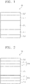
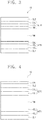
- FIGS. 1 to 4 are schematic cross-sectional views illustrating organic electroluminescence devices according to embodiments of the inventive concept.
- a first electrode EL1 and a second electrode EL2 are disposed to face each other and an emission layer EML may be disposed between the first electrode EL1 and the second electrode EL2.
- Each of the organic electroluminescence devices 10 of the embodiments may further comprise functional layers between the first electrode EL1 and the second electrode EL2 in addition to the emission layer EML.
- the functional layers may comprise a hole transport region HTR and an electron transport region ETR.
- each of the organic electroluminescence devices 10 according to embodiments may comprise the first electrode EL1, the hole transport region HTR, the emission layer EML, the electron transport region ETR, and the second electrode EL2 that may be sequentially stacked.
- the organic electroluminescence device 10 of an embodiment may comprise a capping layer CPL disposed on the second electrode EL2.
- the organic electroluminescence device 10 of an embodiment may comprise a compound according to an embodiment described below in the emission layer EML disposed between the first electrode EL1 and the second electrode EL2.
- the organic electroluminescence device 10 of an embodiment may comprise a compound according to an embodiment described below in the hole transport region HTR or the electron transport region ETR which is one of the functional layers disposed between the first electrode EL1 and the second electrode EL2, as well as in the emission layer EML.
- FIG. 2 illustrates a schematic cross-sectional view of an organic electroluminescence device 10 of an embodiment, in which a hole transport region HTR comprises a hole injection layer HIL and a hole transport layer HTL, and an electron transport region ETR comprises an electron injection layer EIL and an electron transport layer ETL.
- FIG. 3 illustrates a schematic cross-sectional view of an organic electroluminescence device 10 of an embodiment, in which a hole transport region HTR comprises a hole injection layer HIL, a hole transport layer HTL, and an electron blocking layer EBL, and an electron transport region ETR comprises an electron injection layer EIL, an electron transport layer ETL, and a hole blocking layer HBL.
- FIG. 4 illustrates a schematic cross-sectional view of an organic electroluminescence device 10 of an embodiment comprising a capping layer CPL disposed on the second electrode EL2.
- the first electrode EL1 has a conductivity.
- the first electrode EL1 may be formed of a metal alloy or a conductive compound.
- the first electrode EL1 may be an anode.
- the first electrode EL1 may be a pixel electrode.
- the first electrode EL1 may be a transmissive electrode, a transflective electrode, or a reflective electrode.
- the first electrode EL1 may comprise a transparent metal oxide, such as indium tin oxide (ITO), indium zinc oxide (IZO), zinc oxide (ZnO), and indium tin zinc oxide (ITZO).
- the first electrode EL1 When the first electrode EL1 is a transflective electrode or a reflective electrode, the first electrode EL1 may include Ag, Mg Cu, Al, Pt, Pd, Au, Ni, Nd, Ir, Cr, Li, Ca, LiF/Ca, LiF/Al, Mo, Ti, a compound thereof, or a mixture thereof (e.g., a mixture of Ag and Mg). In other embodiments, the first electrode EL1 may have a multilayer structure comprising a reflective layer or a transflective layer formed of the above-described materials, and a transparent conductive layer formed of ITO, IZO, ZnO, ITZO, etc.
- the first electrode EL1 may have a three-layer structure of ITO/Ag/ITO, but is not limited thereto.
- the thickness of the first electrode EL1 may be in a range of about 1,000 ⁇ to about 10,000 ⁇ .
- the thickness of the first electrode EL1 may be in a range of about 1,000 ⁇ to about 3,000 ⁇ .
- the hole transport region HTR may be provided on the first electrode EL1.
- the hole transport region HTR may comprise at least one of a hole injection layer HIL, a hole transport layer HTL, a hole buffer layer (not shown), or an electron blocking layer.
- the thickness of the hole transport region HTR may be, for example, in a range of about 50 ⁇ to about 15,000 ⁇ .
- the hole transport region HTR may have a single layer formed of a single material, a single layer formed of different materials, or a multilayer structure including layers formed of different materials.
- the hole transport region HTR may have a single layer structure of a hole injection layer HIL or a hole transport layer HTL, and may have a single layer structure formed of a hole injection material and a hole transport material.
- the hole transport region HTR may have a single layer structure formed of different materials, or it may have a structure in which a hole injection layer HIL/hole transport layer HTL, a hole injection layer HIL/hole transport layer HTL/hole buffer layer (not shown), a hole injection layer HIL/hole buffer layer (not shown), a hole transport layer HTL/hole buffer layer, or a hole injection layer HIL/hole transport layer HTL/electron blocking layer EBL are stacked in order from the first electrode EL1, but an embodiment is not limited thereto.
- the hole transport region HTR may be formed using various methods such as a vacuum deposition method, a spin coating method, a cast method, a Langmuir-Blodgett (LB) method, an inkjet printing method, a laser printing method, and a laser induced thermal imaging (LITI) method.
- a vacuum deposition method such as a vacuum deposition method, a spin coating method, a cast method, a Langmuir-Blodgett (LB) method, an inkjet printing method, a laser printing method, and a laser induced thermal imaging (LITI) method.
- LB Langmuir-Blodgett
- LITI laser induced thermal imaging
- the hole injection layer HIL may include, for example, a phthalocyanine compound such as copper phthalocyanine; N,N'-diphenyl-N,N'-bis-[4-(phenyl-m-tolyl-amino)-phenyl]-biphenyl-4,4'-diamine (DNTPD), 4,4',4"-[tris(3-methylphenyl)phenylamino]triphenylamine] (m-MTDATA), 4,4',4"-tris(N,N-diphenylamino)triphenylamine (TDATA), 4,4',4''-tris ⁇ N,-(2-naphthyl) -N-phenylamino)-triphenylamine (2-TNATA), poly(3,4-ethylenedioxythiophene)/poly(4-styrenesulfonate) (PEDOT/PSS), polyaniline/dodecylbenzenesulfonic acid (P
- the hole transport layer HTL may include, for example, carbazole derivatives such as N-phenyl carbazole and polyvinyl carbazole, fluorene derivatives, N4,N4'-di(naphthalen-1-yl)-N4,N4'-diphenyl-[1,1'-biphenyl]-4,4'-diamine (a-NPD), N,N'-bis(3-methylphenyl)-N,N'-diphenyl-[1,1-biphenyl]-4,4'-diamine (TPD), triphenylamine derivatives such as 4,4',4"-tris(N-carbazolyl)triphenylamine (TCTA), N,N'-di(naphthalene-1-yl)-N,N'-diphenyl-benzidine (NPB), 4,4'-cyclohexylidene bis[N,N-bis(4-methylphenyl)benzenamine] (TAPC), 4,4'-
- the electron blocking layer EBL may include, for example, 9-phenyl-9H-3,9'-bicarbazole (CCP), 1,3-bis(N-carbazolyl)benzene (mCP), 1,3-bis(1,8-dimethyl-9H-carbazol-9-yl)benzene (mDCP), etc.
- CCP 9-phenyl-9H-3,9'-bicarbazole
- mCP 1,3-bis(N-carbazolyl)benzene
- mDCP 1,3-bis(1,8-dimethyl-9H-carbazol-9-yl)benzene
- the thickness of the hole transport region HTR may be in a range of about 50 ⁇ to about 10,000 ⁇ .
- the thickness of the hole transport region HTR may be in a range of about 100 ⁇ to about 5,000 ⁇ .
- the thickness of the hole injection layer HIL may be, for example, in a range of about 30 ⁇ to about 1,000 ⁇
- the thickness of the hole transport layer HTL may be in a range of about 30 ⁇ to about 1,000 ⁇ .
- the thickness of the electron blocking layer EBL may be in a range of about 10 ⁇ to about 1,000 ⁇ . If the thicknesses of the hole transport region HTR, the hole injection layer HIL, the hole transport layer HTL, and the electron blocking layer EBL satisfy the above-described ranges, satisfactory hole transport properties may be achieved without a substantial increase in driving voltage.
- the hole transport region HTR may further comprise a charge generating material to increase conductivity.
- the charge generating material may be dispersed uniformly or non-uniformly in the hole transport region HTR.
- the charge generating material may be, for example, a p-dopant.
- the p-dopant may be one of quinone derivatives, metal oxides, or cyano group-containing compounds, but is not limited thereto.
- non-limiting examples of the p-dopant may include, but are not limited to, quinone derivatives such as tetracyanoquinodimethane (TCNQ) and 2,3,5,6-tetrafluoro-7,7,8,8-tetracyanoquinodimethane (F4-TCNQ), metal oxides such as tungsten oxides and molybdenum oxides.
- quinone derivatives such as tetracyanoquinodimethane (TCNQ) and 2,3,5,6-tetrafluoro-7,7,8,8-tetracyanoquinodimethane (F4-TCNQ)
- metal oxides such as tungsten oxides and molybdenum oxides.
- the hole transport region HTR may further comprise at least one of a hole buffer layer (not shown) or an electron blocking layer EBL in addition to the hole injection layer HIL and the hole transport layer HTL.
- the hole buffer layer (not shown), may compensate a resonance distance according to the wavelength of light emitted from an emission layer EML and may increase light emission efficiency.
- Materials which may be included in the hole transport region HTR may be used as materials which may be included in the hole buffer layer (not shown).
- the electron blocking layer EBL is a layer that serves may serve to prevent electrons from being injected from the electron transport region ETR to the hole transport region HTR.
- the emission layer EML is provided on the hole transport region HTR.
- the thickness of the emission layer EML may be in a range of about 100 ⁇ to about 1000 ⁇ .
- the thickness of the emission layer EML may be in a range of about 100 ⁇ to about 300 ⁇ .
- the emission layer EML may have a single layer formed of a single material, a single layer formed of different materials, or a multilayer structure having layers formed of different materials.
- the emission layer EML in the organic electroluminescence device 10 of an embodiment may comprise a compound of an embodiment.
- the compound according to an embodiment may comprise at least one azasiline unit and at least one condensed cyclic unit comprising a boron atom (B).
- the condensed cyclic unit may comprise two heteroatoms selected from among an oxygen atom (O) and a sulfur atom (S) in addition to the boron atom.
- the condensed cyclic unit may have a structure in which five hexacyclic rings are condensed, and the heteroatom may comprise a boron atom.
- the azasiline unit may comprise one azasiline moiety, or may have a spiro structure in which two azasiline moieties are bonded.
- the compound of an embodiment may comprise a condensed cyclic unit containing a boron atom as an electron acceptor, and an azasiline unit as an electron donor.
- the compound of an embodiment may have a structure in which at least one electron acceptor and at least one electron donor are bonded.
- substituted or unsubstituted may indicate that one is substituted or unsubstituted with at least one substituent selected from the group consisting of a deuterium atom, a halogen atom, a cyano group, a nitro group, an amino group, a silyl group, an oxy group, a thio group, a sulfinyl group, a sulfonyl group, a carbonyl group, a boryl group, a phosphine oxide group, a phosphine sulfide group, an alkyl group, an alkenyl group, an alkynyl group, an alkoxy group, a hydrocarbon ring group, an aryl group, and a heterocyclic group.
- substituents described above may be substituted or unsubstituted.
- a biphenyl group may be interpreted as an aryl group or a phenyl group
- examples of the halogen atom may comprise a fluorine atom, a chlorine atom, a bromine atom, and an iodine atom.
- the alkyl group may be a linear, branched or cyclic type.
- the number of carbons in the alkyl group is 1 to 50, 1 to 30, 1 to 20, 1 to 10, or 1 to 6.
- Examples of the alkyl group may include, but are not limited to, methyl group, ethyl group, n-propyl group, isopropyl group, n-butyl group, s-butyl group, t-butyl group, i-butyl group, 2-ethylbutyl group, 3,3-dimethylbutyl group, n-pentyl group, i-pentyl group, neopentyl group, t-pentyl group, cyclopentyl group, 1-methylpentyl group, 3-methylpentyl group, 2-ethylpentyl group, 4-methyl-2-pentyl group, n-hexyl group, 1-methylhexyl group, 2-ethylhexy
- an aryl group means any functional group or substituent derived from an aromatic hydrocarbon ring.
- the aryl group may be a monocyclic aryl group or a polycyclic aryl group.
- the number of ring-forming carbon atoms in the aryl group may be 6 to 30, 6 to 20, or 6 to 15.
- aryl group may include phenyl, naphthyl, fluorenyl, anthracenyl, phenanthryl, biphenyl, terphenyl, quaterphenyl, quinquephenyl, sexiphenyl, triphenylenyl, pyrenyl, benzofluoranthenyl, chrysenyl, etc., but are not limited thereto.
- the heteroaryl group may include at least one of B, O, N, P, Si, or S as a heteroatom.
- the heteroaryl group may contain two or more heteroatoms, the two or more heteroatoms may be the same as or different from each other.
- the heteroaryl group may be a monocyclic heteroaryl group or a polycyclic heteroaryl group.
- the number of ring-forming carbon atoms in the heteroaryl group may be 2 to 30, 2 to 20, or 2 to 10.
- heteroaryl group may include thiophene, furan, pyrrole, imidazole, thiazole, oxazole, oxadiazole, triazole, pyridyl, bipyridyl, pyrimidyl, triazine, triazole, acridyl, pyridazine, pyrazinyl, quinolinyl, quinazoline, quinoxalinyl, phenoxazyl, phthalazinyl, pyrido pyrimidyl, pyrido pyrazinyl, pyrazino pyrazinyl, isoquinoline, indole, carbazole, N-arylcarbazole, N-heteroarylcarbazole, N-alkylcarbazole, benzoxazole, benzoimidazole, benzothiazole, benzocarbazole, benzothiophene, dibenzothiophen
- the silyl group includes an alkyl silyl group and an aryl silyl group.
- Examples of the silyl group may include, but are not limited to, trimethylsilyl, triethylsilyl, t-butyldimethylsilyl, propyldimethylsilyl, triphenylsilyl, diphenylsilyl, phenylsilyl, etc.
- the number of carbon atoms in an amine group is not specifically limited, but may be 1 to 30.
- the amine group may include an alkyl amine group and an aryl amine group. Examples of the amine group may include, but are not limited to, methylamine group, dimethylamine group, phenylamine group, diphenylamine group, naphthylamine group, 9-methyl-anthracenylamine group, triphenylamine group, etc.
- the boron group includes an alkyl boron group and an aryl boron group.
- Examples of the boron group may include, but are not limited to, trimethylboron, triethylboron, t-butyldimethylboron, triphenylboron, diphenylboron, phenylboron, etc.
- the alkyl group in the alkylaryl group, the alkyl boron group, the alkyl silyl group, and the alkyl amine group is the same as examples of the alkyl group described above.
- the aryl group in the aryl boron group, the aryl silyl group, and the aryl amine group is the same as examples of the aryl group described above.
- the emission layer EML in the organic electroluminescence device 10 of an embodiment may comprise a compound represented by Formula 1.
- X 1 and X 2 may each independently be O or S.
- both X 1 and X 2 may be O
- both X 1 and X 2 may be S
- one among X 1 and X 2 may be O, and the other may be S.
- L 1 to L 11 may be a substituent represented by Formula 2-a or Formula 2-b.
- one selected from L 1 to L 11 , two selected from L 1 to L 11 , or three selected from L 1 to L 11 may be a substituent represented by Formula 2-a or Formula 2-b.
- L 1 to L 11 is a substituent represented by Formula 2-a or Formula 2-b
- the remainder of L 1 to L 11 may each independently be a hydrogen atom, a deuterium atom, a halogen atom, a cyano group, a substituted or unsubstituted amine group, a substituted or unsubstituted silyl group, a substituted or unsubstituted boron group, a substituted or unsubstituted linear or branched alkyl group having 1 to 20 carbon atoms, a substituted or unsubstituted aryl group having 6 to 30 ring-forming carbon atoms, or a substituted or unsubstituted heteroaryl group having 2 to 30 ring-forming carbon atoms.
- L 1 to L 11 in the case where one of L 1 to L 11 is a substituent represented by Formula 2-a or Formula 2-b, the remainder of L 1 to L 11 may each independently be a hydrogen atom, a deuterium atom, a fluorine atom, a cyano group, an aryl amine group, an aryl silyl group, an aryl boron group, a linear alkyl group, a branched alkyl group, an unsubstituted aryl group, an aryl group substituted with a deuterium atom, or an unsubstituted heteroaryl group.
- the embodiments are not limited thereto.
- L 1 to L 11 are cyclic alkyl groups may be excluded.
- At least one of L 1 to L 11 may be represented by Formula 2-a or Formula 2-b:
- R 1 to R 24 may each independently be a hydrogen atom, a deuterium atom, a halogen atom, a cyano group, a substituted or unsubstituted amine group, a substituted or unsubstituted silyl group, a substituted or unsubstituted boron group, a substituted or unsubstituted alkyl group having 1 to 20 carbon atoms, a substituted or unsubstituted aryl group having 6 to 30 ring-forming carbon atoms, or a substituted or unsubstituted heteroaryl group having 2 to 30 ring-forming carbon atoms.
- R 1 to R 24 may each independently be a hydrogen atom, a deuterium atom, a fluorine atom, a cyano group, an aryl amine group, an aryl silyl group, an aryl boron group, a linear alkyl group, a branched alkyl group, an unsubstituted aryl group, an aryl group substituted with a deuterium atom, or an unsubstituted heteroaryl group, etc.
- the embodiments are not limited thereto.
- Ar 1 and Ar 2 may each independently be a substituted or unsubstituted alkyl group having 1 to 20 carbon atoms, a substituted or unsubstituted aryl group having 6 to 30 ring-forming carbon atoms, or a substituted or unsubstituted heteroaryl group having 2 to 30 ring-forming carbon atoms.
- Ar 1 and Ar 2 may each independently be an unsubstituted phenyl group, a phenyl group substituted with a deuterium atom, an unsubstituted biphenyl group, an unsubstituted naphthyl group, or an unsubstituted dibenzothiophene group.
- Ar 1 and Ar 2 may be the same as or different from each other. However, the embodiments are not limited thereto.
- Ar 3 is a substituted or unsubstituted alkyl group having 1 to 20 carbon atoms, a substituted or unsubstituted aryl group having 6 to 30 ring-forming carbon atoms, a substituted or unsubstituted heteroaryl group having 2 to 30 ring-forming carbon atoms, or a substituent represented by Formula 1.
- L 1 to L 11 in Ar 3 may each independently be a hydrogen atom, a deuterium atom, a halogen atom, a cyano group, a substituted or unsubstituted amine group, a substituted or unsubstituted silyl group, a substituted or unsubstituted boron group, a substituted or unsubstituted linear or branched alkyl group having 1 to 20 carbon atoms, a substituted or unsubstituted aryl group having 6 to 30 ring-forming carbon atoms, or a substituted or unsubstituted heteroaryl group having 2 to 30 ring-forming carbon atoms.
- Formula 2-b
- At least one hydrogen atom may be substituted with a deuterium atom.
- all the hydrogen atoms in the compound of an embodiment may be substituted with deuterium atoms.
- a substituent represented by Formula 2-a or Formula 2-b in the compound represented by Formula 1 of an embodiment may be excluded, and all the other hydrogen atoms may be substituted with deuterium atoms.
- all the hydrogen atoms in a substituent represented by Formula 2-a or Formula 2-b bonded to Formula 1 may be substituted with deuterium atoms.
- the compound represented by Formula 1 of an embodiment may be represented by one of Formula 1-1 to Formula 1-3.
- Formula 1-1 to Formula 1-3 represent examples according to the combination of heteroatoms contained in the condensed cyclic unit.
- the compound of an embodiment may include the condensed cyclic unit containing oxaborine or thiaborine as represented by Formula 1-1 to Formula 1-3 below:
- L 1 to L 11 may be the same as defined in Formula 1.
- the compound of an embodiment may include, as an electron acceptor, the condensed cyclic unit containing oxaborine or thiaborine.
- the compound represented by Formula 1 of an embodiment may be represented by one of Formula 1A to Formula IE.
- DU may be represented by Formula 2-a or Formula 2-b as described above.
- Formula 1A to Formula IE show embodiments according to the azasiline unit's bonding site represented by DU and the number of the bonded azasiline units.
- a to c may each independently be an integer from 0 to 3.
- X 1 and X 2 may be the same as defined in Formula 1.
- La to L c and L 1 to L 11 may each independently be a hydrogen atom, a deuterium atom, a halogen atom, a cyano group, a substituted or unsubstituted amine group, a substituted or unsubstituted silyl group, a substituted or unsubstituted boron group, a substituted or unsubstituted linear or branched alkyl group having 1 to 20 carbon atoms, a substituted or unsubstituted aryl group having 6 to 30 ring-forming carbon atoms, or a substituted or unsubstituted heteroaryl group having 2 to 30 ring-forming carbon atoms.
- La to L c and L 1 to L 11 may each independently be a hydrogen atom, a deuterium atom, a fluorine atom, a cyano group, an aryl amine group, an aryl silyl group, an aryl boron group, a linear alkyl group, a branched alkyl group, an unsubstituted aryl group, an aryl group substituted with a deuterium atom, or an unsubstituted heteroaryl group, etc.
- the compound represented by Formula 1 of an embodiment may be represented by Formula IF:
- R 9 to R 24 may be the same as defined in Formula 2-b, AU is a substituent represented by Formula 1, and the case where AU is substituted with a substituent represented by Formula 2-a or Formula 2-b above is excluded. For example, AU is not substituted with a substituent represented by Formula 2-a or Formula 2-b.
- R 9 to R 24 may each independently be a hydrogen atom, a deuterium atom, a fluorine atom, a cyano group, an aryl amine group, an aryl silyl group, an aryl boron group, a linear alkyl group, a branched alkyl group, an unsubstituted aryl group, an aryl group substituted with a deuterium atom, or an unsubstituted heteroaryl group, etc.
- the embodiments are not limited thereto.
- Formula IF shows an embodiment having a structure containing the azasiline unit represented by Formula 2-b and the condensed cyclic unit represented by Formula 1.
- the compound represented by Formula IF of an embodiment may have a structure containing two electron acceptor units which may be represented by Formula 1 and one electron donor unit which may be represented by Formula 2-b.
- the compound represented by Formula 1 of an embodiment may be represented by one of Formula 1F-1 to Formula 1F-3.
- Formula 1F-1 to Formula 1F-3 show embodiments having a structure containing the azasiline unit represented by Formula 2-b and the condensed cyclic unit represented by Formula 1.
- Formula 1F-1 to Formula 1F-3 show embodiments having different bonding sites of the condensed cyclic units bonded to the azasiline units.
- L 1 to L 11 may each independently be a hydrogen atom, a deuterium atom, a halogen atom, a cyano group, a substituted or unsubstituted amine group, a substituted or unsubstituted silyl group, a substituted or unsubstituted boron group, a substituted or unsubstituted linear or branched alkyl group having 1 to 20 carbon atoms, a substituted or unsubstituted aryl group having 6 to 30 ring-forming carbon atoms, or a substituted or unsubstituted heteroaryl group having 2 to 30 ring-forming carbon atoms.
- X 1 and X 2 may be the same as defined in Formula 1
- R 9 to R 24 may be the same as defined in Formula 2-b.
- the compound of an embodiment as described above has a molecular structure in which a condensed cyclic unit containing a boron atom and an azasiline unit are bonded, and thus a charge separation state in a molecule may be maintained at an appropriate level to facilitate reverse intersystem crossing. Therefore, the compound of an embodiment may have small ⁇ E ST values to exhibit improved fluorescence efficiency. For example, if the compound according to an embodiment is used as an emission layer material of the organic electroluminescence device, a light emission efficiency characteristic of the organic electroluminescence device may be improved.
- the compound of an embodiment has a compound molecular structure in which the reverse intersystem crossing easily occurs by bonding at least one electron acceptor and at least one electron donor, and thereby may be used as a thermally activated delayed fluorescence (TADF) material.
- TADF thermally activated delayed fluorescence
- the compound of an embodiment may be used as a TADF dopant material emitting blue light.
- the compound represented by Formula 1 of an embodiment may be a luminescent material having a luminescence center wavelength ( ⁇ max ) in a wavelength region of less than or equal to about 490 nm.
- the compound represented by Formula 1 of an embodiment may be a luminescent material having a luminescence center wavelength in a wavelength region in a range of about 430 nm to about 490 nm.
- the compound represented by Formula 1 of an embodiment may be a blue thermally activated delayed fluorescence dopant.
- the compound of an embodiment may be used as a TADF material emitting deep blue light.
- the compound of an embodiment may be selected from one of the compounds represented by Compound Group 1, which includes Compounds 1 to 234.
- the electroluminescence device 10 of an embodiment may include at least one compound represented by Compound Group 1 in the emission layer EML.
- “Ph” represents a phenyl group.
- At least one of the hydrogen atoms in the compound of an embodiment may be substituted with a deuterium atom.
- any hydrogen atom in a compound according to an embodiment may be substituted with a deuterium atom.
- the compound of an embodiment may have the same form as Compound 1-d corresponding to that in which a hydrogen atom is substituted with a deuterium atom in Compound 1 of Compound Group 1, and although not listed, the form in which any hydrogen atom is substituted with a deuterium atom may be equally provided for compounds in other embodiments described in Compound Group 1.
- the emission layer EML in the organic electroluminescence device 10 comprising the compound of an embodiment may emit a delayed fluorescence.
- the emission layer EML may emit a thermally activated delayed fluorescence (TADF).
- TADF thermally activated delayed fluorescence
- the organic electroluminescence device 10 of an embodiment may comprise multiple emission layers.
- the emission layers may be sequentially stacked and provided.
- the organic electroluminescence device 10 comprising the emission layers may emit white light.
- the organic electroluminescence device comprising emission layers may be an organic electroluminescence device having a tandem structure.
- at least one emission layer EML may include the above-described compound of an embodiment.
- the emission layer EML may comprise a host and a dopant, and may comprise the above-described compound of an embodiment as a dopant.
- the emission layer EML in the organic electroluminescence device 10 of an embodiment may comprise host for emitting a delayed fluorescence and a dopant for emitting a delayed fluorescence, and may comprise the above-described compound of an embodiment as a dopant for emitting a delayed fluorescence.
- the emission layer EML may comprise at least one of the compounds represented by Compound Group 1 as described above as a thermally activated delayed fluorescence dopant.
- the emission layer EML may be a delayed fluorescence emission layer, and the emission layer EML may comprise a known host material and the above-described compound.
- the compound of an embodiment may be used as a TADF dopant.
- the emission layer may comprise known host materials.
- the emission layer EML may include, as a host material, tris(8-hydroxyquinolino)aluminum (Alq 3 ), 4,4'-bis(N-carbazolyl)-1,1'-biphenyl (CBP), poly(N-vinylcabazole) (PVK), 9,10-di(naphthalene-2-yl)anthracene (ADN), 4,4',4"-tris(carbazol-9-yl)-triphenylamine (TCTA), 1,3,5-tris(1-phenyl-1H-benzo[d]imidazol-2-yl)benzene (TPBi), 3-tert-butyl-9,10-di(naphth-2-yl)anthracene (TBADN), distyrylarylene (DSA), 4,4'-bis(9-carbazolyl)-2,2'-dimethyl
- the emission layer EML in the organic electroluminescence device 10 of an embodiment may further comprise known dopant materials.
- the emission layer EML may further comprise, as dopant materials, styryl derivatives (e.g., 1, 4-bis[2-(3-N-ethylcarbazolyl)vinyl]benzene (BCzVB), 4-(di-p-tolylamino)-4'-[(di-p-tolylamino)styryl]stilbene (DPAVB), and N-(4-((E)-2-(6-((E)-4-(diphenylamino)styryl)naphthalen-2-yl)vinyl)phenyl)-N-phenylbenzena mine (N-BDAVBi), perylene and the derivatives thereof (e.g., 2,5,8,11-tetra-t-butylperylene (TBP)), pyrene and the derivatives thereof (e.g., 1-dipyrene
- the electron transport region ETR is provided on the emission layer EML.
- the electron transport region ETR may comprise at least one of a hole blocking layer HBL, an electron transport layer ETL, or an electron injection layer EIL, but an embodiment is not limited thereto.
- the electron transport region ETR may have a single layer formed of a single material, a single layer formed of different materials, or a multilayer structure including layers formed of different materials.
- the electron transport region ETR may have a single layer structure of an electron injection layer EIL or an electron transport layer ETL, and may have a single layer structure formed of an electron injection material and an electron transport material.
- the electron transport region ETR may have a single layer structure formed of different materials, or may have a structure in which an electron transport layer ETL/electron injection layer EIL and a hole blocking layer HBL/electron transport layer ETL/electron injection layer EIL are stacked in order from the emission layer EML, but is not limited thereto.
- the thickness of the electron transport region ETR may be, for example, in a range of about 1000 ⁇ to about 1,500 ⁇ .
- the electron transport region ETR may be formed using various methods such as a vacuum deposition method, a spin coating method, a cast method, a Langmuir-Blodgett (LB) method, an inkjet printing method, a laser printing method, a laser induced thermal imaging (LITI) method, etc.
- a vacuum deposition method such as a vacuum deposition method, a spin coating method, a cast method, a Langmuir-Blodgett (LB) method, an inkjet printing method, a laser printing method, a laser induced thermal imaging (LITI) method, etc.
- LB Langmuir-Blodgett
- LITI laser induced thermal imaging
- the electron transport region ETR may include an anthracene-based compound.
- the embodiments are not limited thereto, and the electron transport region may include, for example, tris(8-hydroxyquinolinato)aluminum (Alq 3 ), 1,3,5-tri[(3-pyridyl)-phen-3-yl]benzene, 2,4,6-tris(3'-(pyridin-3-yl)biphenyl-3-yl)-1,3,5-triazine, 2-(4-(N-phenylbenzoimidazol-1-yl)phenyl)-9, 10-dinaphthylanthracene, 1,3,5-Tri(1-phenyl-1H-benzo[d]imidazol-2-yl)benzene (TPBi), 2,9-dimethyl-4,7-diphenyl-1,10-phenanthroline (BCP), 4,7-diphenyl-1,10-phen
- the thickness of the electron transport layers ETL may be in a range of about 100 ⁇ to about 1,000 ⁇ .
- the thickness of the electron transport layers ETL may be in a range of about 150 ⁇ to about 500 ⁇ . If the thickness of the electron transport layers ETL satisfies the above-described range, satisfactory electron transport characteristics may be obtained without a substantial increase in driving voltage.
- the electron transport region ETR may be formed using metal halides such as LiF, NaCl, CsF, RbCl, RbI, and CuI, lanthanum metals such as Yb, co-deposition of the metal halides and the lanthanum metals (e.g., KI:Yb or RbI:Yb, etc.), metal oxides such as Li 2 O and BaO, lithium quinolato (LiQ), etc., but the embodiments are not limited thereto.
- the electron injection layer EIL may also be formed of a mixture material of an electron transport material and an insulating organo-metal salt.
- the organo-metal salt may be a material having an energy band gap of greater than or equal to about 4 eV.
- the organo-metal salt may include metal acetates, metal benzoates, metal acetoacetates, metal acetylacetonates or metal stearates.
- the thickness of the electron injection layer EIL may be in a range of about 1 ⁇ to about 100 ⁇ .
- the thickness of the electron injection layer EIL may be in a range of about 3 ⁇ to about 90 ⁇ . If the thickness of the electron injection layers EIL satisfies the above-described range, satisfactory electron injection properties may be obtained without a substantial increase in driving voltage.
- the electron transport region ETR may include a hole blocking layer HBL as described above.
- the hole blocking layer HBL may include, for example, at least one of 2,9-dimethyl-4,7-diphenyl-1,10-phenanthroline (BCP), 4,7-diphenyl-1,10-phenanthroline (Bphen), DPEPO, and PPF, but is not limited thereto.
- the second electrode EL2 is provided on the electron transport region ETR.
- the second electrode EL2 may be a common electrode or cathode.
- the second electrode EL2 may be a transmissive electrode, a transflective electrode, or a reflective electrode.
- the second electrode EL2 may include a transparent metal oxide, for example, ITO, IZO, ZnO, ITZO, etc.
- the second electrode EL2 When the second electrode EL2 is a transflective electrode or a reflective electrode, the second electrode EL2 may include Ag, Mg, Cu, Al, Pt, Pd, Au, Ni, Nd, Ir, Cr, Li, Ca, LiF/Ca, LiF/Al, Mo, Ti, Yb, a compound thereof, or a mixture thereof (e.g., AgMg, AgYb). In other embodiments, the second electrode EL2 may have a multilayer structure including a reflective layer or a transflective layer formed of the above-described materials, and a transparent conductive layer formed of ITO, IZO, ZnO, ITZO, etc.
- the second electrode EL2 may be connected to an auxiliary electrode. If the second electrode EL2 is connected with the auxiliary electrode, the resistance of the second electrode EL2 may decrease.
- a capping layer CPL may be further disposed on the second electrode EL2 of the organic electroluminescence device 10 according to an embodiment.
- the refractive index of the capping layer CPL may be greater than or equal to about 1.6.
- the refractive index of the capping layer CPL may be greater than or equal to about 1.6 at a wavelength of about 589 nm.
- the capping layer CPL may be an organic layer or an inorganic layer.
- the inorganic material may comprise an alkaline metal compound such as LiF, an alkaline earth metal compound such as MgF2, SiON, SiNx, SiOy, etc.
- the organic material when the capping layer CPL includes an organic material, the organic material may include ⁇ -NPD, NPB, TPD, m-MTDATA, Alq 3 , CuPc, N4,N4,N4',N4'-tetra(biphenyl-4-yl)biphenyl-4,4'-diamine (TPD15), 4,4',4"-tris(carbazol -9-yl)triphenylamine (TCTA), etc., or an epoxy resin, or acrylate such as methacrylate.
- the embodiments are not limited thereto, and the organic material may also include Compounds P1 to P5 below.
- a capping layer CPL may include an amine compound.
- the capping layer CPL may include at least one of Compound CPL1 or Compound CPL2 below:
- the organic electroluminescence device 10 may comprise the above-described compound of an embodiment in the emission layer EML disposed between the first electrode EL1 and the second electrode EL2 to exhibit excellent light emission efficiency.
- the organic electroluminescence device of an embodiment may exhibit high light emission efficiency in an emission wavelength region of blue light.
- the compound according to an embodiment may be a thermally activated delayed fluorescence dopant, and the emission layer EML may comprise the compound of an embodiment to emit a thermally activated delayed fluorescence, thereby exhibiting good light emission efficiency characteristics.
- the above-described compound of an embodiment may be included as a material for the organic electroluminescence device 10 in a functional layer in addition to the emission layer EML.
- the organic electroluminescence device 10 of an embodiment of the inventive concept may also include the above-described compound in at least one functional layer disposed between the first electrode EL1 and the second electrode EL2, or in the capping layer CPL disposed on the second electrode EL2.
- the organic electroluminescence device When the above-described compound of an embodiment is used as a material of the organic electroluminescence device by including an azasiline unit and a condensed cyclic unit containing an oxaborine or a thiaborine ring essentially containing a boron atom (B), efficiency of the organic electroluminescence device may be more improved. Furthermore, the organic electroluminescence device of an embodiment including the compound of an embodiment in the emission layer may emit deep blue light and exhibit high efficiency characteristics.
- a synthesis method for a compound according to an example will be described in detail by illustrating a synthetic method of Compounds 1, 55, and 60.
- a compound synthesis method is provided as an example, but the synthetic method for a compound according to an embodiment of the inventive concept is not limited to Examples below.
- Compound 1 according to an example may be synthesized by, for example, the steps shown in Reaction Scheme 1 below:
- Compound 55 according to an example may be synthesized by, for example, the steps shown in Reaction Formula 2 below:
- the crude product was purified by a silica gel column chromatography (using eluent having a 2:1 volume ratio of hexane and chloroform) to obtain Compound 55 which is a light yellow solid (0.14 g, yield 14%).
- Compound 55 was identified with NMR analysis.
- Compound 60 according to an example may be synthesized by, for example, the steps shown in Reaction Formula 3 below:
- the crude product was purified by a silica gel column chromatography (using eluent having a 2:1 volume ratio of hexane and chloroform) to obtain Compound 60 which is a light yellow solid (0.12 g, yield 11%).
- Compound 60 was identified with NMR analysis.
- Example Compounds have small ⁇ E ST values and thus may be used as a thermally activated delayed fluorescence dopant. It is believed that Example Compounds have smaller ⁇ E ST values compared to Comparative Example Compounds, and thus Example Compounds exhibit improved light emission emitting efficiency characteristics compared to Comparative Example Compounds.
- Example and Comparative Example Compounds the fluorescence quantum yield and fluorescence lifetime were evaluated.
- Samples for evaluation of fluorescence characteristics were prepared by depositing, on a quartz substrate, a composition including Example and Comparative Example Compounds for evaluation to form an organic film. Evaluation of the prepared samples were performed in an inert gas atmosphere. In the preparation of samples, DPEPO or PPF was used as a host material. In the prepared sample composition, an Example or Comparative Example Compound was contained to be 12 wt% to 50wt% based on the total weight of the composition.
- Example Compounds emit deep blue light having the maximum emission wavelength of less than or equal to about 490 nm. It may be confirmed that Example Compounds exhibit fluorescence efficiency of 80% or greater to exhibit good light emission efficiency characteristics.
- the Example Compounds exhibit smaller delay time (Tau delay) compared to Comparative Example Compounds, and thus it may be predicted that delayed fluorescence efficiency of Example Compounds is more increased compared to Comparative Example Compounds.
- An evaluation of the organic electroluminescence device of an embodiment including the compound of an embodiment in the emission layer was carried out as follows. The method for manufacturing the organic electroluminescence device for the evaluation of the device is described below.
- Comparative Examples 1 and 2 are the organic electroluminescence devices manufactured by using each of Comparative Example Compounds C1 and C2 as a dopant material of the emission layer, respectively.
- the organic electroluminescence devices of Examples and Comparative Examples were manufactured as follows.
- An ITO was patterned on a glass substrate to form a first electrode.
- HAT-CN was deposited to a thickness of about 100 ⁇ to form a hole injection layer
- TAPC was deposited to a thickness of about 500 ⁇ to form a hole transport layer
- a 100 ⁇ -thick electron blocking layer EBL was formed with mDCP.
- an Example Compound and PPF were co-deposited in a ratio of about 20:80 to form a 200 ⁇ -thick layer.
- the emission layer formed by co-depositing was deposited by mixing an Example Compound and PPF.
- a 100 ⁇ -thick layer was formed on the emission layer by using PPF, a 300 ⁇ -thick layer was formed with B3PyPB, and a 10 ⁇ -thick layer was formed with LiF to form an electron transport region.
- a second electrode having a thickness of about 1,000 ⁇ was formed with aluminum (Al).
- the organic electroluminescence devices of Examples emit light in a blue wavelength region of less than or equal to about 480 nm to exhibit high light emission efficiency characteristics. It may be confirmed that Examples 1 to 3 exhibit higher external quantum efficiency values compared to Comparative Examples.
- the compound of an example may include at least one condensed cyclic unit containing a boron atom and at least one azasiline unit bonded to the condensed cyclic unit to facilitate the reverse intersystem crossing, thereby exhibiting excellent light emission efficiency.
- the organic electroluminescence device of an example may include the compound of an example in the emission layer to exhibit high light emission efficiency in a deep blue emission wavelength region.
- the organic electroluminescence device of an embodiment may exhibit excellent light emission efficiency.
- the compound of an embodiment may be contained in the emission layer of the organic electroluminescence device to contribute to high efficiency of the organic electroluminescence device.
Landscapes
- Chemical & Material Sciences (AREA)
- Engineering & Computer Science (AREA)
- Materials Engineering (AREA)
- Physics & Mathematics (AREA)
- Spectroscopy & Molecular Physics (AREA)
- Organic Chemistry (AREA)
- Optics & Photonics (AREA)
- Electroluminescent Light Sources (AREA)
- Inorganic Chemistry (AREA)
Abstract
Description
- This application claims priority to and benefits of Korean Patent Application No.
10-2020-0052327 filed on April 29, 2020 - The disclosure relates to a compound used as a luminescence material and an organic electroluminescence device including the same.
- Recently, active development is being conducted for an organic electroluminescence display as an image display device. In contrast to liquid crystal display devices and the like, the organic electroluminescence display is a so-called self-luminescent display device in which holes and electrons injected from a first electrode and a second electrode recombine in an emission layer, and thus a luminescent material including an organic compound in the emission layer emits light to implement display.
- In the application of an organic electroluminescence device to a display device, there is a continuous demand for an organic electroluminescence device having a low driving voltage, high light emission efficiency, and a long service life, and for the development of materials for an organic electroluminescence device that is capable of stably attaining such characteristics.
- In order to implement a highly efficient organic electroluminescence device in recent years, technologies pertaining to phosphorescence emission using triplet state energy or delayed fluorescence using triplet-triplet annihilation (TTA) in which singlet excitons are generated by collision of triplet excitons are being developed, and thermally activated delayed fluorescence (TADF) materials using delayed fluorescence phenomenon are being developed.
- The disclosure provides an organic electroluminescence device exhibiting excellent light emission efficiency.
- The disclosure also provides a compound which is a material for an organic electroluminescence device emitting deep-blue light and having high efficiency characteristics.
- An embodiment of the inventive concept provides a compound represented by Formula 1:

- In Formula 1, X1 and X2 may each independently be O or S, and at least one of L1 to L11 may be a substituent represented by Formula 2-a or Formula 2-b, the remainder of L1 to L11 may each independently be a hydrogen atom, a deuterium atom, a halogen atom, a cyano group, a substituted or unsubstituted amine group, a substituted or unsubstituted silyl group, a substituted or unsubstituted boron group, a substituted or unsubstituted linear or branched alkyl group having 1 to 20 carbon atoms, a substituted or unsubstituted aryl group having 6 to 30 ring-forming carbon atoms, or a substituted or unsubstituted heteroaryl group having 2 to 30 ring-forming carbon atoms.


- In Formula 2-a and Formula 2-b, R1 to R24 may each independently be a hydrogen atom, a deuterium atom, a halogen atom, a cyano group, a substituted or unsubstituted amine group, a substituted or unsubstituted silyl group, a substituted or unsubstituted boron group, a substituted or unsubstituted alkyl group having 1 to 20 carbon atoms, a substituted or unsubstituted aryl group having 6 to 30 ring-forming carbon atoms, or a substituted or unsubstituted heteroaryl group having 2 to 30 ring-forming carbon atoms. Ar1 and Ar2 may each independently be a substituted or unsubstituted alkyl group having 1 to 20 carbon atoms, a substituted or unsubstituted aryl group having 6 to 30 ring-forming carbon atoms, or a substituted or unsubstituted heteroaryl group having 2 to 30 ring-forming carbon atoms, and Ar3 may be a substituted or unsubstituted alkyl group having 1 to 20 carbon atoms, a substituted or unsubstituted aryl group having 6 to 30 ring-forming carbon atoms, a substituted or unsubstituted heteroaryl group having 2 to 30 ring-forming carbon atoms, or a substituent represented by Formula 1. When Ar3 is a substituent represented by Formula 1, L1 to L11 in Ar3 may each independently be a hydrogen atom, a deuterium atom, a halogen atom, a cyano group, a substituted or unsubstituted amine group, a substituted or unsubstituted silyl group, a substituted or unsubstituted boron group, a substituted or unsubstituted linear or branched alkyl group having 1 to 20 carbon atoms, a substituted or unsubstituted aryl group having 6 to 30 ring-forming carbon atoms, or a substituted or unsubstituted heteroaryl group having 2 to 30 ring-forming carbon atoms.
- In an embodiment, Formula 1 may be represented by one of Formula 1-1 to Formula 1-3:


- In Formula 1-1 to Formula 1-3, L1 to L11 may be the same as defined in Formula 1.
- In an embodiment, Formula 1 may be represented by one of Formula 1A to Formula IE:


- In Formula 1A to Formula IE, a to c may each independently be an integer from 0 to 3, X1 and X2 may be the same as defined in Formula 1, La to Lc and L1 to L11 may each independently be a hydrogen atom, a deuterium atom, a halogen atom, a cyano group, a substituted or unsubstituted amine group, a substituted or unsubstituted silyl group, a substituted or unsubstituted boron group, a substituted or unsubstituted linear or branched alkyl group having 1 to 20 carbon atoms, a substituted or unsubstituted aryl group having 6 to 30 ring-forming carbon atoms, or a substituted or unsubstituted heteroaryl group having 2 to 30 ring-forming carbon atoms, and DU may be represented by Formula 2-a or Formula 2-b.
- In an embodiment, Formula 1 may be represented by Formula 1F:


- In Formula IF, R9 to R24 may be the same as defined in Formula 2-b, AU may be a substituent represented by Formula 1, except that AU may not be substituted with a substituent represented by Formula 2-a or Formula 2-b.
- In an embodiment, Formula 1 may be represented by one of Formula 1F-1 to Formula 1F-3:


- In Formula 1F-1 to Formula 1F-3, L1 to L11 may each independently be a hydrogen atom, a deuterium atom, a halogen atom, a cyano group, a substituted or unsubstituted amine group, a substituted or unsubstituted silyl group, a substituted or unsubstituted boron group, a substituted or unsubstituted linear or branched alkyl group having 1 to 20 carbon atoms, a substituted or unsubstituted aryl group having 6 to 30 ring-forming carbon atoms, or a substituted or unsubstituted heteroaryl group having 2 to 30 ring-forming carbon atoms, X1 and X2 may be the same as defined in Formula 1, and R9 to R24 may be the same as defined in Formula 2-b.
- In an embodiment, in Formula 1, at least one hydrogen atom may be substituted with a deuterium atom.
- In an embodiment, in Formula 1, Ar1 and Ar2 may each independently be an unsubstituted phenyl group, a phenyl group substituted with a deuterium atom, an unsubstituted biphenyl group, an unsubstituted naphthyl group, or an unsubstituted dibenzothiophene group.
- In an embodiment, the compound represented by Formula 1 may be a blue luminescent material.
- In an embodiment, the compound represented by Formula 1 may be a thermally activated delayed fluorescence emitting material.
- Another embodiment of the inventive concept provides an organic electroluminescence device comprising a first electrode, a second electrode disposed on the first electrode, and an emission layer disposed between the first electrode and the second electrode. The emission layer may comprise a compound represented by Formula 1.
- In an embodiment, the organic electroluminescence device may further comprise a capping layer disposed on the second electrode, and the capping layer may have a refractive index of greater than or equal to about 1.6.
- In an embodiment, the emission layer may be a delayed fluorescence emission layer comprising a host and a dopant, and the dopant may comprise the compound represented by Formula 1.
- In an embodiment, the emission layer may emit blue light having a center wavelength in a range of about 430 nm to about 490 nm.
- The accompanying drawings are included to provide a further understanding of the inventive concept, and are incorporated in and constitute a part of this specification. The drawings illustrate embodiments of the inventive concept and, together with the description, serve to explain principles of the inventive concept. In the drawings:
-
FIG. 1 is a schematic cross-sectional view illustrating an organic electroluminescence device according to an embodiment of the inventive concept; and -
FIG. 2 is a schematic cross-sectional view illustrating an organic electroluminescence device according to an embodiment of the inventive concept. -
FIG. 3 is a schematic cross-sectional view illustrating an organic electroluminescence device according to an embodiment of the inventive concept; and -
FIG. 4 is a schematic cross-sectional view illustrating an organic electroluminescence device according to an embodiment of the inventive concept. - The inventive concept may have various modifications and may be embodied in different forms, and example embodiments will be explained in detail with reference to the accompanying drawings. The inventive concept may, however, be embodied in different forms and should not be construed as limited to the embodiments set forth herein. Rather, all modifications, equivalents, and substituents which are included in the spirit and technical scope of the inventive concept should be included in the inventive concept.
- In the description, it will be understood that when an element (a region, a layer, a section, or the like) is referred to as being "on", "connected to" or "coupled to" another element, it can be directly on, connected or coupled to the other element, or an intervening third element may be disposed therebetween.
- Like reference numerals refer to like elements throughout the specification. In the drawings, the thickness, the ratio, and the dimensions of elements may be exaggerated for an effective description of technical contents.
- As used herein, the term "and/or" includes any and all combinations of one or more of the associated listed items. For example, "A and/or B" may be understood to mean "A, B, or A and B." The terms "and" and "or" may be used in the conjunctive or disjunctive sense and may be understood to be equivalent to "and/or". Throughout the disclosure, the expression "at least one of A, B, and C" may indicate only A, only B, only C, both A and B, both A and C, both B and C, all of A, B, and C, or variations thereof.
- The term "at least one of' is intended to include the meaning of "at least one selected from" for the purpose of its meaning and interpretation. For example, "at least one of A and B" may be understood to mean "A, B, or A and B." When preceding a list of elements, the term, "at least one of," modifies the entire list of elements and does not modify the individual elements of the list.
- It will be understood that, although the terms "first", "second", etc. may be used herein to describe various elements, these elements should not be limited by these terms. These terms are only used to distinguish one element from another. For example, a first element could be termed a second element, and, similarly, a second element could be termed a first element, without departing from the scope of the embodiments of the inventive concept. The terms of a singular form may include plural forms unless the context clearly indicates otherwise.
- The terms "below," "lower," "above," "upper," and the like are used to describe the relationship of the configurations shown in the drawings. The terms are used as a relative concept and are described with reference to the direction indicated in the drawings.
- The terms "about" or "approximately" as used herein is inclusive of the stated value and means within an acceptable range of deviation for the recited value as determined by one of ordinary skill in the art, considering the measurement in question and the error associated with measurement of the recited quantity (i.e., the limitations of the measurement system). For example, "about" may mean within one or more standard deviations, or within ± 20%, 10%, or 5% of the stated value.
- Unless otherwise defined, all terms (including technical and scientific terms) used herein have the same meaning as commonly understood by one of ordinary skill in the art to which the inventive concept pertains. It is also to be understood that terms defined in commonly used dictionaries should be interpreted as having meanings consistent with the meanings in the context of the related art, and are expressly defined herein unless they are interpreted in an ideal or overly formal sense.
- It should be understood that the terms "comprises," "comprising," "includes," "including," "have," "having," "contains," and/or "containing" are intended to specify the presence of stated features, integers, steps, operations, elements, components, or combinations thereof in the disclosure, but do not preclude the presence or addition of one or more other features, integers, steps, operations, elements, components, or combinations thereof.
- Hereinafter, an organic electroluminescence device according to an embodiment of the inventive concept and a compound of an embodiment included therein will be described with reference to the accompanying drawings.
-
FIGS. 1 to 4 are schematic cross-sectional views illustrating organic electroluminescence devices according to embodiments of the inventive concept. Referring toFIGS. 1 to 4 , in each oforganic electroluminescence devices 10 according to embodiments, a first electrode EL1 and a second electrode EL2 are disposed to face each other and an emission layer EML may be disposed between the first electrode EL1 and the second electrode EL2. - Each of the
organic electroluminescence devices 10 of the embodiments may further comprise functional layers between the first electrode EL1 and the second electrode EL2 in addition to the emission layer EML. The functional layers may comprise a hole transport region HTR and an electron transport region ETR. For example, each of theorganic electroluminescence devices 10 according to embodiments may comprise the first electrode EL1, the hole transport region HTR, the emission layer EML, the electron transport region ETR, and the second electrode EL2 that may be sequentially stacked. Theorganic electroluminescence device 10 of an embodiment may comprise a capping layer CPL disposed on the second electrode EL2. - The
organic electroluminescence device 10 of an embodiment may comprise a compound according to an embodiment described below in the emission layer EML disposed between the first electrode EL1 and the second electrode EL2. However, embodiments are not limited thereto, and theorganic electroluminescence device 10 of an embodiment may comprise a compound according to an embodiment described below in the hole transport region HTR or the electron transport region ETR which is one of the functional layers disposed between the first electrode EL1 and the second electrode EL2, as well as in the emission layer EML. - In comparison to
FIG. 1, FIG. 2 illustrates a schematic cross-sectional view of anorganic electroluminescence device 10 of an embodiment, in which a hole transport region HTR comprises a hole injection layer HIL and a hole transport layer HTL, and an electron transport region ETR comprises an electron injection layer EIL and an electron transport layer ETL. In comparison toFIG. 1 ,FIG. 3 illustrates a schematic cross-sectional view of anorganic electroluminescence device 10 of an embodiment, in which a hole transport region HTR comprises a hole injection layer HIL, a hole transport layer HTL, and an electron blocking layer EBL, and an electron transport region ETR comprises an electron injection layer EIL, an electron transport layer ETL, and a hole blocking layer HBL. In comparison toFIG. 2 ,FIG. 4 illustrates a schematic cross-sectional view of anorganic electroluminescence device 10 of an embodiment comprising a capping layer CPL disposed on the second electrode EL2. - The first electrode EL1 has a conductivity. The first electrode EL1 may be formed of a metal alloy or a conductive compound. The first electrode EL1 may be an anode. The first electrode EL1 may be a pixel electrode. The first electrode EL1 may be a transmissive electrode, a transflective electrode, or a reflective electrode. When the first electrode EL1 is a transmissive electrode, the first electrode EL1 may comprise a transparent metal oxide, such as indium tin oxide (ITO), indium zinc oxide (IZO), zinc oxide (ZnO), and indium tin zinc oxide (ITZO). When the first electrode EL1 is a transflective electrode or a reflective electrode, the first electrode EL1 may include Ag, Mg Cu, Al, Pt, Pd, Au, Ni, Nd, Ir, Cr, Li, Ca, LiF/Ca, LiF/Al, Mo, Ti, a compound thereof, or a mixture thereof (e.g., a mixture of Ag and Mg). In other embodiments, the first electrode EL1 may have a multilayer structure comprising a reflective layer or a transflective layer formed of the above-described materials, and a transparent conductive layer formed of ITO, IZO, ZnO, ITZO, etc. For example, the first electrode EL1 may have a three-layer structure of ITO/Ag/ITO, but is not limited thereto. The thickness of the first electrode EL1 may be in a range of about 1,000 Å to about 10,000 Å. For example, the thickness of the first electrode EL1 may be in a range of about 1,000 Å to about 3,000 Å.
- The hole transport region HTR may be provided on the first electrode EL1. The hole transport region HTR may comprise at least one of a hole injection layer HIL, a hole transport layer HTL, a hole buffer layer (not shown), or an electron blocking layer. The thickness of the hole transport region HTR may be, for example, in a range of about 50 Å to about 15,000 Å.
- The hole transport region HTR may have a single layer formed of a single material, a single layer formed of different materials, or a multilayer structure including layers formed of different materials.
- For example, the hole transport region HTR may have a single layer structure of a hole injection layer HIL or a hole transport layer HTL, and may have a single layer structure formed of a hole injection material and a hole transport material. The hole transport region HTR may have a single layer structure formed of different materials, or it may have a structure in which a hole injection layer HIL/hole transport layer HTL, a hole injection layer HIL/hole transport layer HTL/hole buffer layer (not shown), a hole injection layer HIL/hole buffer layer (not shown), a hole transport layer HTL/hole buffer layer, or a hole injection layer HIL/hole transport layer HTL/electron blocking layer EBL are stacked in order from the first electrode EL1, but an embodiment is not limited thereto.
- The hole transport region HTR may be formed using various methods such as a vacuum deposition method, a spin coating method, a cast method, a Langmuir-Blodgett (LB) method, an inkjet printing method, a laser printing method, and a laser induced thermal imaging (LITI) method.
- The hole injection layer HIL may include, for example, a phthalocyanine compound such as copper phthalocyanine; N,N'-diphenyl-N,N'-bis-[4-(phenyl-m-tolyl-amino)-phenyl]-biphenyl-4,4'-diamine (DNTPD), 4,4',4"-[tris(3-methylphenyl)phenylamino]triphenylamine] (m-MTDATA), 4,4',4"-tris(N,N-diphenylamino)triphenylamine (TDATA), 4,4',4''-tris{N,-(2-naphthyl) -N-phenylamino)-triphenylamine (2-TNATA), poly(3,4-ethylenedioxythiophene)/poly(4-styrenesulfonate) (PEDOT/PSS), polyaniline/dodecylbenzenesulfonic acid (PANI/DBSA), polyaniline/camphor sulfonic acid (PANI/CSA), polyaniline/poly(4-styrenesulfonate) (PANI/PSS), N,N'-di(naphthalene-1-yl)-N,N'-diphenyl-benzidine (NPB), triphenylamine-containing polyetherketone (TPAPEK), 4-isopropyl-4'-methyldiphenyliodonium tetrakis(pentafluorophenyl)borate, dipyrazino[2,3-f: 2',3'-h]quinoxaline-2,3,6,7,10,11-hexacarbonitrile (HAT-CN), etc.
- The hole transport layer HTL may include, for example, carbazole derivatives such as N-phenyl carbazole and polyvinyl carbazole, fluorene derivatives, N4,N4'-di(naphthalen-1-yl)-N4,N4'-diphenyl-[1,1'-biphenyl]-4,4'-diamine (a-NPD), N,N'-bis(3-methylphenyl)-N,N'-diphenyl-[1,1-biphenyl]-4,4'-diamine (TPD), triphenylamine derivatives such as 4,4',4"-tris(N-carbazolyl)triphenylamine (TCTA), N,N'-di(naphthalene-1-yl)-N,N'-diphenyl-benzidine (NPB), 4,4'-cyclohexylidene bis[N,N-bis(4-methylphenyl)benzenamine] (TAPC), 4,4'-bis[N,N'-(3-tolyl)amino]-3,3'-dimethylbiphenyl (HMTPD), 1,3-bis(N-carbazolyl)benzene (mCP), etc.
- The electron blocking layer EBL may include, for example, 9-phenyl-9H-3,9'-bicarbazole (CCP), 1,3-bis(N-carbazolyl)benzene (mCP), 1,3-bis(1,8-dimethyl-9H-carbazol-9-yl)benzene (mDCP), etc.
- The thickness of the hole transport region HTR may be in a range of about 50 Å to about 10,000 Å. For example, the thickness of the hole transport region HTR may be in a range of about 100 Å to about 5,000 Å. The thickness of the hole injection layer HIL may be, for example, in a range of about 30 Å to about 1,000 Å, and the thickness of the hole transport layer HTL may be in a range of about 30 Å to about 1,000 Å. For example, the thickness of the electron blocking layer EBL may be in a range of about 10 Å to about 1,000 Å. If the thicknesses of the hole transport region HTR, the hole injection layer HIL, the hole transport layer HTL, and the electron blocking layer EBL satisfy the above-described ranges, satisfactory hole transport properties may be achieved without a substantial increase in driving voltage.
- The hole transport region HTR may further comprise a charge generating material to increase conductivity. The charge generating material may be dispersed uniformly or non-uniformly in the hole transport region HTR. The charge generating material may be, for example, a p-dopant. The p-dopant may be one of quinone derivatives, metal oxides, or cyano group-containing compounds, but is not limited thereto. For example, non-limiting examples of the p-dopant may include, but are not limited to, quinone derivatives such as tetracyanoquinodimethane (TCNQ) and 2,3,5,6-tetrafluoro-7,7,8,8-tetracyanoquinodimethane (F4-TCNQ), metal oxides such as tungsten oxides and molybdenum oxides.
- As described above, the hole transport region HTR may further comprise at least one of a hole buffer layer (not shown) or an electron blocking layer EBL in addition to the hole injection layer HIL and the hole transport layer HTL. The hole buffer layer (not shown), may compensate a resonance distance according to the wavelength of light emitted from an emission layer EML and may increase light emission efficiency. Materials which may be included in the hole transport region HTR may be used as materials which may be included in the hole buffer layer (not shown). The electron blocking layer EBL is a layer that serves may serve to prevent electrons from being injected from the electron transport region ETR to the hole transport region HTR.
- The emission layer EML is provided on the hole transport region HTR. The thickness of the emission layer EML may be in a range of about 100 Å to about 1000 Å. For example, the thickness of the emission layer EML may be in a range of about 100 Å to about 300 Å. The emission layer EML may have a single layer formed of a single material, a single layer formed of different materials, or a multilayer structure having layers formed of different materials.
- The emission layer EML in the
organic electroluminescence device 10 of an embodiment may comprise a compound of an embodiment. - The compound according to an embodiment may comprise at least one azasiline unit and at least one condensed cyclic unit comprising a boron atom (B). In the compound according to an embodiment, the condensed cyclic unit may comprise two heteroatoms selected from among an oxygen atom (O) and a sulfur atom (S) in addition to the boron atom. In the compound of an embodiment, the condensed cyclic unit may have a structure in which five hexacyclic rings are condensed, and the heteroatom may comprise a boron atom.
- In the compound of an embodiment, the azasiline unit may comprise one azasiline moiety, or may have a spiro structure in which two azasiline moieties are bonded.
- The compound of an embodiment may comprise a condensed cyclic unit containing a boron atom as an electron acceptor, and an azasiline unit as an electron donor. The compound of an embodiment may have a structure in which at least one electron acceptor and at least one electron donor are bonded.
- In the description, the term "substituted or unsubstituted" may indicate that one is substituted or unsubstituted with at least one substituent selected from the group consisting of a deuterium atom, a halogen atom, a cyano group, a nitro group, an amino group, a silyl group, an oxy group, a thio group, a sulfinyl group, a sulfonyl group, a carbonyl group, a boryl group, a phosphine oxide group, a phosphine sulfide group, an alkyl group, an alkenyl group, an alkynyl group, an alkoxy group, a hydrocarbon ring group, an aryl group, and a heterocyclic group. Each of the substituents described above may be substituted or unsubstituted. For example, a biphenyl group may be interpreted as an aryl group or a phenyl group substituted with a phenyl group.
- In the description, examples of the halogen atom may comprise a fluorine atom, a chlorine atom, a bromine atom, and an iodine atom.
- In the description, the alkyl group may be a linear, branched or cyclic type. The number of carbons in the alkyl group is 1 to 50, 1 to 30, 1 to 20, 1 to 10, or 1 to 6. Examples of the alkyl group may include, but are not limited to, methyl group, ethyl group, n-propyl group, isopropyl group, n-butyl group, s-butyl group, t-butyl group, i-butyl group, 2-ethylbutyl group, 3,3-dimethylbutyl group, n-pentyl group, i-pentyl group, neopentyl group, t-pentyl group, cyclopentyl group, 1-methylpentyl group, 3-methylpentyl group, 2-ethylpentyl group, 4-methyl-2-pentyl group, n-hexyl group, 1-methylhexyl group, 2-ethylhexyl group, 2-butylhexyl group, cyclohexyl group, 4-methylcyclohexyl group, 4-t-butylcyclohexyl group, n-heptyl group, 1-methylheptyl group, 2,2-dimethylheptyl group, 2-ethylheptyl group, 2-butylheptyl group, n-octyl group, t-octyl group, 2-ethyloctyl group, 2-butyloctyl group, 2-hexyloctyl group, 3,7-dimethyloctyl group, cyclooctyl group, n-nonyl group, n-decyl group, adamantyl group, 2-ethyldecyl group, 2-butyldecyl group, 2-hexyldecyl group, 2-octyldecyl group, n-undecyl group, n-dodecyl group, 2-ethyldodecyl group, 2-butyldodecyl group, 2-hexyldocecyl group, 2-octyldodecyl group, n-tridecyl group, n-tetradecyl group, n-pentadecyl group, n-hexadecyl group, 2-ethylhexadecyl group, 2-butylhexadecyl group, 2-hexylhexadecyl group, 2-octylhexadecyl group, n-heptadecyl group, n-octadecyl group, n-nonadecyl group, n-eicosyl group, 2-ethyleicosyl group, 2-butyleicosyl group, 2-hexyleicosyl group, 2-octyleicosyl group, n-heneicosyl group, n-docosyl group, n-tricosyl group, n-tetracosyl group, n-pentacosyl group, n-hexacosyl group, n-heptacosyl group, n-octacosyl group, n-nonacosyl group, n-triacontyl group, etc.
- In the description, an aryl group means any functional group or substituent derived from an aromatic hydrocarbon ring. The aryl group may be a monocyclic aryl group or a polycyclic aryl group. The number of ring-forming carbon atoms in the aryl group may be 6 to 30, 6 to 20, or 6 to 15. Examples of the aryl group may include phenyl, naphthyl, fluorenyl, anthracenyl, phenanthryl, biphenyl, terphenyl, quaterphenyl, quinquephenyl, sexiphenyl, triphenylenyl, pyrenyl, benzofluoranthenyl, chrysenyl, etc., but are not limited thereto.
- In the description, the heteroaryl group may include at least one of B, O, N, P, Si, or S as a heteroatom. When the heteroaryl group contains two or more heteroatoms, the two or more heteroatoms may be the same as or different from each other. The heteroaryl group may be a monocyclic heteroaryl group or a polycyclic heteroaryl group. The number of ring-forming carbon atoms in the heteroaryl group may be 2 to 30, 2 to 20, or 2 to 10. Examples of the heteroaryl group may include thiophene, furan, pyrrole, imidazole, thiazole, oxazole, oxadiazole, triazole, pyridyl, bipyridyl, pyrimidyl, triazine, triazole, acridyl, pyridazine, pyrazinyl, quinolinyl, quinazoline, quinoxalinyl, phenoxazyl, phthalazinyl, pyrido pyrimidyl, pyrido pyrazinyl, pyrazino pyrazinyl, isoquinoline, indole, carbazole, N-arylcarbazole, N-heteroarylcarbazole, N-alkylcarbazole, benzoxazole, benzoimidazole, benzothiazole, benzocarbazole, benzothiophene, dibenzothiophenyl, thienothiophene, benzofuranyl, phenanthroline, thiazolyl, isooxazolyl, oxadiazolyl, thiadiazolyl, phenothiazolyl, phenothiazinyl, dibenzosilole, dibenzofuranyl, etc., but are not limited thereto.
- In the description, the silyl group includes an alkyl silyl group and an aryl silyl group. Examples of the silyl group may include, but are not limited to, trimethylsilyl, triethylsilyl, t-butyldimethylsilyl, propyldimethylsilyl, triphenylsilyl, diphenylsilyl, phenylsilyl, etc.
- In the description, the number of carbon atoms in an amine group is not specifically limited, but may be 1 to 30. The amine group may include an alkyl amine group and an aryl amine group. Examples of the amine group may include, but are not limited to, methylamine group, dimethylamine group, phenylamine group, diphenylamine group, naphthylamine group, 9-methyl-anthracenylamine group, triphenylamine group, etc.
- In the description, the boron group includes an alkyl boron group and an aryl boron group. Examples of the boron group may include, but are not limited to, trimethylboron, triethylboron, t-butyldimethylboron, triphenylboron, diphenylboron, phenylboron, etc.
- In the description, the alkyl group in the alkylaryl group, the alkyl boron group, the alkyl silyl group, and the alkyl amine group is the same as examples of the alkyl group described above.
- In the description, the aryl group in the aryl boron group, the aryl silyl group, and the aryl amine group is the same as examples of the aryl group described above.
- In the description, "" refers to a binding site to a neighboring atom.

- The emission layer EML in the
organic electroluminescence device 10 of an embodiment may comprise a compound represented by Formula 1.

- In Formula 1, X1 and X2 may each independently be O or S. For example, both X1 and X2 may be O, both X1 and X2 may be S, or one among X1 and X2 may be O, and the other may be S.
- In Formula 1, at least one of L1 to L11 may be a substituent represented by Formula 2-a or Formula 2-b. For example, in Formula 1, one selected from L1 to L11, two selected from L1 to L11, or three selected from L1 to L11 may be a substituent represented by Formula 2-a or Formula 2-b.
- In the case where one of L1 to L11 is a substituent represented by Formula 2-a or Formula 2-b, and the remainder of L1 to L11 may each independently be a hydrogen atom, a deuterium atom, a halogen atom, a cyano group, a substituted or unsubstituted amine group, a substituted or unsubstituted silyl group, a substituted or unsubstituted boron group, a substituted or unsubstituted linear or branched alkyl group having 1 to 20 carbon atoms, a substituted or unsubstituted aryl group having 6 to 30 ring-forming carbon atoms, or a substituted or unsubstituted heteroaryl group having 2 to 30 ring-forming carbon atoms.
- For example, in Formula 1, in the case where one of L1 to L11 is a substituent represented by Formula 2-a or Formula 2-b, the remainder of L1 to L11 may each independently be a hydrogen atom, a deuterium atom, a fluorine atom, a cyano group, an aryl amine group, an aryl silyl group, an aryl boron group, a linear alkyl group, a branched alkyl group, an unsubstituted aryl group, an aryl group substituted with a deuterium atom, or an unsubstituted heteroaryl group. However, the embodiments are not limited thereto. The case where L1 to L11 are cyclic alkyl groups may be excluded.
- In the compound represented by Formula 1 of an embodiment, at least one of L1 to L11 may be represented by Formula 2-a or Formula 2-b:


- In Formula 2-a and Formula 2-b, R1 to R24 may each independently be a hydrogen atom, a deuterium atom, a halogen atom, a cyano group, a substituted or unsubstituted amine group, a substituted or unsubstituted silyl group, a substituted or unsubstituted boron group, a substituted or unsubstituted alkyl group having 1 to 20 carbon atoms, a substituted or unsubstituted aryl group having 6 to 30 ring-forming carbon atoms, or a substituted or unsubstituted heteroaryl group having 2 to 30 ring-forming carbon atoms. For example, in Formula 2-a and Formula 2-b, R1 to R24 may each independently be a hydrogen atom, a deuterium atom, a fluorine atom, a cyano group, an aryl amine group, an aryl silyl group, an aryl boron group, a linear alkyl group, a branched alkyl group, an unsubstituted aryl group, an aryl group substituted with a deuterium atom, or an unsubstituted heteroaryl group, etc. However, the embodiments are not limited thereto.
- In Formula 2-a, Ar1 and Ar2 may each independently be a substituted or unsubstituted alkyl group having 1 to 20 carbon atoms, a substituted or unsubstituted aryl group having 6 to 30 ring-forming carbon atoms, or a substituted or unsubstituted heteroaryl group having 2 to 30 ring-forming carbon atoms. For example, Ar1 and Ar2 may each independently be an unsubstituted phenyl group, a phenyl group substituted with a deuterium atom, an unsubstituted biphenyl group, an unsubstituted naphthyl group, or an unsubstituted dibenzothiophene group. Ar1 and Ar2 may be the same as or different from each other. However, the embodiments are not limited thereto.
- In Formula 2-b, Ar3 is a substituted or unsubstituted alkyl group having 1 to 20 carbon atoms, a substituted or unsubstituted aryl group having 6 to 30 ring-forming carbon atoms, a substituted or unsubstituted heteroaryl group having 2 to 30 ring-forming carbon atoms, or a substituent represented by Formula 1.
- In Formula 2-b, when Ar3 is a substituent represented by Formula 1 as described above, the case where L1 to L11 in Ar3 are azasiline units represented by Formula 2-a or Formula 2-b may be excluded. For example, in Formula 2-b, when Ar3 is a substituent represented by Formula 1 as described above, L1 to L11 in Ar3 may each independently be a hydrogen atom, a deuterium atom, a halogen atom, a cyano group, a substituted or unsubstituted amine group, a substituted or unsubstituted silyl group, a substituted or unsubstituted boron group, a substituted or unsubstituted linear or branched alkyl group having 1 to 20 carbon atoms, a substituted or unsubstituted aryl group having 6 to 30 ring-forming carbon atoms, or a substituted or unsubstituted heteroaryl group having 2 to 30 ring-forming carbon atoms. In Formula 2-b, Ar3 may be a substituted or unsubstituted phenyl group. For example, Ar3 may be a substituent represented by Formula 1 as described above, or an unsubstituted phenyl group.
- In the compound of an embodiment, at least one hydrogen atom may be substituted with a deuterium atom. For example, all the hydrogen atoms in the compound of an embodiment may be substituted with deuterium atoms. For example, a substituent represented by Formula 2-a or Formula 2-b in the compound represented by Formula 1 of an embodiment may be excluded, and all the other hydrogen atoms may be substituted with deuterium atoms. For example, all the hydrogen atoms in a substituent represented by Formula 2-a or Formula 2-b bonded to Formula 1 may be substituted with deuterium atoms.
- The compound represented by Formula 1 of an embodiment may be represented by one of Formula 1-1 to Formula 1-3. Formula 1-1 to Formula 1-3 represent examples according to the combination of heteroatoms contained in the condensed cyclic unit. For example, the compound of an embodiment may include the condensed cyclic unit containing oxaborine or thiaborine as represented by Formula 1-1 to Formula 1-3 below:

- In Formula 1-1 to Formula 1-3, L1 to L11 may be the same as defined in Formula 1.
- The compound of an embodiment may include, as an electron acceptor, the condensed cyclic unit containing oxaborine or thiaborine.
- The compound represented by Formula 1 of an embodiment may be represented by one of Formula 1A to Formula IE. In Formula 1A to Formula IE, DU may be represented by Formula 2-a or Formula 2-b as described above. Formula 1A to Formula IE show embodiments according to the azasiline unit's bonding site represented by DU and the number of the bonded azasiline units.
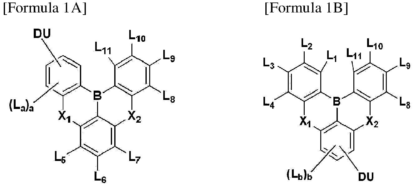

- In Formula 1A to Formula 1E, a to c may each independently be an integer from 0 to 3. In Formula 1A to Formula 1E, X1 and X2 may be the same as defined in Formula 1. In Formula 1A to Formula 1E, La to Lc and L1 to L11 may each independently be a hydrogen atom, a deuterium atom, a halogen atom, a cyano group, a substituted or unsubstituted amine group, a substituted or unsubstituted silyl group, a substituted or unsubstituted boron group, a substituted or unsubstituted linear or branched alkyl group having 1 to 20 carbon atoms, a substituted or unsubstituted aryl group having 6 to 30 ring-forming carbon atoms, or a substituted or unsubstituted heteroaryl group having 2 to 30 ring-forming carbon atoms. In the compound represented by Formula 1A to Formula IE of an embodiment, the case where La to Lc and L1 to L11 are represented by Formula 2-a or Formula 2-b is excluded.
- For example, in the compound represented by Formula 1A to Formula IE of an embodiment, La to Lc and L1 to L11 may each independently be a hydrogen atom, a deuterium atom, a fluorine atom, a cyano group, an aryl amine group, an aryl silyl group, an aryl boron group, a linear alkyl group, a branched alkyl group, an unsubstituted aryl group, an aryl group substituted with a deuterium atom, or an unsubstituted heteroaryl group, etc.
- The compound represented by Formula 1 of an embodiment may be represented by Formula IF:

- In Formula IF, R9 to R24 may be the same as defined in Formula 2-b, AU is a substituent represented by Formula 1, and the case where AU is substituted with a substituent represented by Formula 2-a or Formula 2-b above is excluded. For example, AU is not substituted with a substituent represented by Formula 2-a or Formula 2-b. For example, in the compound represented by Formula 1F of an embodiment, R9 to R24 may each independently be a hydrogen atom, a deuterium atom, a fluorine atom, a cyano group, an aryl amine group, an aryl silyl group, an aryl boron group, a linear alkyl group, a branched alkyl group, an unsubstituted aryl group, an aryl group substituted with a deuterium atom, or an unsubstituted heteroaryl group, etc. However, the embodiments are not limited thereto.
- Formula IF shows an embodiment having a structure containing the azasiline unit represented by Formula 2-b and the condensed cyclic unit represented by Formula 1. The compound represented by Formula IF of an embodiment may have a structure containing two electron acceptor units which may be represented by Formula 1 and one electron donor unit which may be represented by Formula 2-b.
- The compound represented by Formula 1 of an embodiment may be represented by one of Formula 1F-1 to Formula 1F-3. Formula 1F-1 to Formula 1F-3 show embodiments having a structure containing the azasiline unit represented by Formula 2-b and the condensed cyclic unit represented by Formula 1. Formula 1F-1 to Formula 1F-3 show embodiments having different bonding sites of the condensed cyclic units bonded to the azasiline units.

- In Formula 1F-1 to Formula 1F-3, L1 to L11 may each independently be a hydrogen atom, a deuterium atom, a halogen atom, a cyano group, a substituted or unsubstituted amine group, a substituted or unsubstituted silyl group, a substituted or unsubstituted boron group, a substituted or unsubstituted linear or branched alkyl group having 1 to 20 carbon atoms, a substituted or unsubstituted aryl group having 6 to 30 ring-forming carbon atoms, or a substituted or unsubstituted heteroaryl group having 2 to 30 ring-forming carbon atoms. In Formula 1F-1 to Formula 1F-3, X1 and X2 may be the same as defined in Formula 1, and R9 to R24 may be the same as defined in Formula 2-b.
- The compound of an embodiment as described above has a molecular structure in which a condensed cyclic unit containing a boron atom and an azasiline unit are bonded, and thus a charge separation state in a molecule may be maintained at an appropriate level to facilitate reverse intersystem crossing. Therefore, the compound of an embodiment may have small ΔEST values to exhibit improved fluorescence efficiency. For example, if the compound according to an embodiment is used as an emission layer material of the organic electroluminescence device, a light emission efficiency characteristic of the organic electroluminescence device may be improved.
- The compound of an embodiment has a compound molecular structure in which the reverse intersystem crossing easily occurs by bonding at least one electron acceptor and at least one electron donor, and thereby may be used as a thermally activated delayed fluorescence (TADF) material. For example, the compound of an embodiment may be used as a TADF dopant material emitting blue light. The compound represented by Formula 1 of an embodiment may be a luminescent material having a luminescence center wavelength (λmax) in a wavelength region of less than or equal to about 490 nm. For example, the compound represented by Formula 1 of an embodiment may be a luminescent material having a luminescence center wavelength in a wavelength region in a range of about 430 nm to about 490 nm. The compound represented by Formula 1 of an embodiment may be a blue thermally activated delayed fluorescence dopant. For example, the compound of an embodiment may be used as a TADF material emitting deep blue light.
- The compound of an embodiment may be selected from one of the compounds represented by Compound Group 1, which includes Compounds 1 to 234. The
electroluminescence device 10 of an embodiment may include at least one compound represented by Compound Group 1 in the emission layer EML. In the compounds represented by Compound Group 1, "Ph" represents a phenyl group.


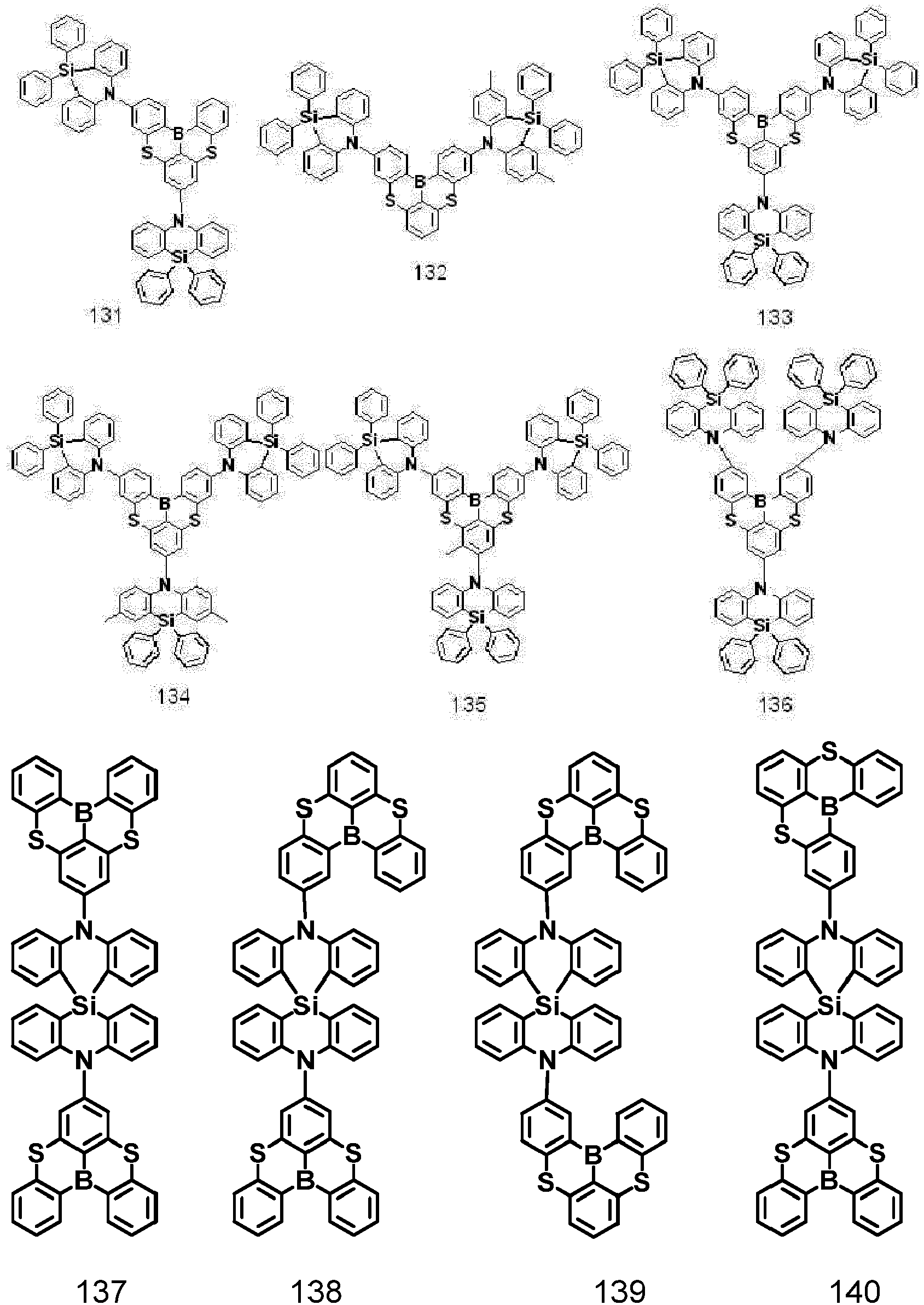


- Although not all listed as an embodiment, at least one of the hydrogen atoms in the compound of an embodiment may be substituted with a deuterium atom. For example, any hydrogen atom in a compound according to an embodiment may be substituted with a deuterium atom.
- For example, the compound of an embodiment may have the same form as Compound 1-d corresponding to that in which a hydrogen atom is substituted with a deuterium atom in Compound 1 of Compound Group 1, and although not listed, the form in which any hydrogen atom is substituted with a deuterium atom may be equally provided for compounds in other embodiments described in Compound Group 1.
- The emission layer EML in the
organic electroluminescence device 10 comprising the compound of an embodiment may emit a delayed fluorescence. For example, the emission layer EML may emit a thermally activated delayed fluorescence (TADF). - Although not shown in the drawings, the
organic electroluminescence device 10 of an embodiment may comprise multiple emission layers. The emission layers may be sequentially stacked and provided. For example, theorganic electroluminescence device 10 comprising the emission layers may emit white light. The organic electroluminescence device comprising emission layers may be an organic electroluminescence device having a tandem structure. When theorganic electroluminescence device 10 comprises multiple emission layers, at least one emission layer EML may include the above-described compound of an embodiment. - In an embodiment, the emission layer EML may comprise a host and a dopant, and may comprise the above-described compound of an embodiment as a dopant. For example, the emission layer EML in the
organic electroluminescence device 10 of an embodiment may comprise host for emitting a delayed fluorescence and a dopant for emitting a delayed fluorescence, and may comprise the above-described compound of an embodiment as a dopant for emitting a delayed fluorescence. The emission layer EML may comprise at least one of the compounds represented by Compound Group 1 as described above as a thermally activated delayed fluorescence dopant. - In an embodiment, the emission layer EML may be a delayed fluorescence emission layer, and the emission layer EML may comprise a known host material and the above-described compound. For example, in the organic electroluminescence device of an embodiment, the compound of an embodiment may be used as a TADF dopant.
- In an embodiment, the emission layer may comprise known host materials. For example, in an embodiment, the emission layer EML may include, as a host material, tris(8-hydroxyquinolino)aluminum (Alq3), 4,4'-bis(N-carbazolyl)-1,1'-biphenyl (CBP), poly(N-vinylcabazole) (PVK), 9,10-di(naphthalene-2-yl)anthracene (ADN), 4,4',4"-tris(carbazol-9-yl)-triphenylamine (TCTA), 1,3,5-tris(1-phenyl-1H-benzo[d]imidazol-2-yl)benzene (TPBi), 3-tert-butyl-9,10-di(naphth-2-yl)anthracene (TBADN), distyrylarylene (DSA), 4,4'-bis(9-carbazolyl)-2,2'-dimethyl-biphenyl (CDBP), 2-methyl-9,10-bis(naphthalen-2-yl)anthracene (MADN), bis[2-(diphenylphosphino)phenyl]ether oxide (DPEPO), hexaphenyl cyclotriphosphazene (CP1), 1,4-bis(triphenylsilyl)benzene (UGH2), hexaphenylcyclotrisiloxane (DPSiO3), octaphenylcyclotetra siloxane (DPSiO4), 2,8-bis(diphenylphosphoryl)dibenzo[b,d]furan (PPF), 3,3'-bis(N-carbazolyl)-1,1'-biphenyl (mCBP), 1,3-bis(N-carbazolyl)benzene (mCP), etc. However, embodiments are not limited thereto, and known delayed fluorescence emission host materials other than the listed host materials may be included.
- The emission layer EML in the
organic electroluminescence device 10 of an embodiment may further comprise known dopant materials. In an embodiment, the emission layer EML may further comprise, as dopant materials, styryl derivatives (e.g., 1, 4-bis[2-(3-N-ethylcarbazolyl)vinyl]benzene (BCzVB), 4-(di-p-tolylamino)-4'-[(di-p-tolylamino)styryl]stilbene (DPAVB), and N-(4-((E)-2-(6-((E)-4-(diphenylamino)styryl)naphthalen-2-yl)vinyl)phenyl)-N-phenylbenzena mine (N-BDAVBi), perylene and the derivatives thereof (e.g., 2,5,8,11-tetra-t-butylperylene (TBP)), pyrene and the derivatives thereof (e.g., 1-dipyrene, 1,4-dipyrenylbenzene, 1,4-bis(N,N-diphenylamino)pyrene), etc. - In the
organic electroluminescence device 10 of an embodiment illustrated inFIGS. 1 to 4 , the electron transport region ETR is provided on the emission layer EML. The electron transport region ETR may comprise at least one of a hole blocking layer HBL, an electron transport layer ETL, or an electron injection layer EIL, but an embodiment is not limited thereto. The electron transport region ETR may have a single layer formed of a single material, a single layer formed of different materials, or a multilayer structure including layers formed of different materials. - For example, the electron transport region ETR may have a single layer structure of an electron injection layer EIL or an electron transport layer ETL, and may have a single layer structure formed of an electron injection material and an electron transport material. The electron transport region ETR may have a single layer structure formed of different materials, or may have a structure in which an electron transport layer ETL/electron injection layer EIL and a hole blocking layer HBL/electron transport layer ETL/electron injection layer EIL are stacked in order from the emission layer EML, but is not limited thereto. The thickness of the electron transport region ETR may be, for example, in a range of about 1000 Å to about 1,500 Å.
- The electron transport region ETR may be formed using various methods such as a vacuum deposition method, a spin coating method, a cast method, a Langmuir-Blodgett (LB) method, an inkjet printing method, a laser printing method, a laser induced thermal imaging (LITI) method, etc.
- When the electron transport region ETR includes the electron transport layer ETL, the electron transport region ETR may include an anthracene-based compound. However, the embodiments are not limited thereto, and the electron transport region may include, for example, tris(8-hydroxyquinolinato)aluminum (Alq3), 1,3,5-tri[(3-pyridyl)-phen-3-yl]benzene, 2,4,6-tris(3'-(pyridin-3-yl)biphenyl-3-yl)-1,3,5-triazine, 2-(4-(N-phenylbenzoimidazol-1-yl)phenyl)-9, 10-dinaphthylanthracene, 1,3,5-Tri(1-phenyl-1H-benzo[d]imidazol-2-yl)benzene (TPBi), 2,9-dimethyl-4,7-diphenyl-1,10-phenanthroline (BCP), 4,7-diphenyl-1,10-phenanthroline (Bphen), 3-(4-biphenylyl)-4-phenyl-5-tert-butylphenyl-1,2,4-triazole (TAZ), 4-(naphthalen-1-yl)-3,5-diphenyl-4H-1,2,4-triazole (NTAZ), 2-(4-biphenylyl)-5-(4-tert-butylphenyl)-1,3,4-oxadiazole (tBu-PBD), bis(2-methyl-8-quinolinolato-N1,O8)-(1,1'-biphenyl-4-olato)aluminum (BAlq), berylliumbis(benzoquinolin-10-olate (Bebq2), 9,10-di(naphthalene-2-yl)anthracene (ADN), 1,3-bis[3,5-di(pyridin-3-yl)phenyl]benzene (B3PyPB), or a mixture thereof. The thickness of the electron transport layers ETL may be in a range of about 100 Å to about 1,000 Å. For example, the thickness of the electron transport layers ETL may be in a range of about 150 Å to about 500 Å. If the thickness of the electron transport layers ETL satisfies the above-described range, satisfactory electron transport characteristics may be obtained without a substantial increase in driving voltage.
- When the electron transport region ETR includes the electron injection layer EIL, the electron transport region ETR may be formed using metal halides such as LiF, NaCl, CsF, RbCl, RbI, and CuI, lanthanum metals such as Yb, co-deposition of the metal halides and the lanthanum metals (e.g., KI:Yb or RbI:Yb, etc.), metal oxides such as Li2O and BaO, lithium quinolato (LiQ), etc., but the embodiments are not limited thereto. The electron injection layer EIL may also be formed of a mixture material of an electron transport material and an insulating organo-metal salt. The organo-metal salt may be a material having an energy band gap of greater than or equal to about 4 eV. For example, the organo-metal salt may include metal acetates, metal benzoates, metal acetoacetates, metal acetylacetonates or metal stearates. The thickness of the electron injection layer EIL may be in a range of about 1 Å to about 100 Å. For example, the thickness of the electron injection layer EIL may be in a range of about 3 Å to about 90 Å. If the thickness of the electron injection layers EIL satisfies the above-described range, satisfactory electron injection properties may be obtained without a substantial increase in driving voltage.
- The electron transport region ETR may include a hole blocking layer HBL as described above. The hole blocking layer HBL may include, for example, at least one of 2,9-dimethyl-4,7-diphenyl-1,10-phenanthroline (BCP), 4,7-diphenyl-1,10-phenanthroline (Bphen), DPEPO, and PPF, but is not limited thereto.
- The second electrode EL2 is provided on the electron transport region ETR. The second electrode EL2 may be a common electrode or cathode. The second electrode EL2 may be a transmissive electrode, a transflective electrode, or a reflective electrode. When the second electrode EL2 is a transmissive electrode, the second electrode EL2 may include a transparent metal oxide, for example, ITO, IZO, ZnO, ITZO, etc.
- When the second electrode EL2 is a transflective electrode or a reflective electrode, the second electrode EL2 may include Ag, Mg, Cu, Al, Pt, Pd, Au, Ni, Nd, Ir, Cr, Li, Ca, LiF/Ca, LiF/Al, Mo, Ti, Yb, a compound thereof, or a mixture thereof (e.g., AgMg, AgYb). In other embodiments, the second electrode EL2 may have a multilayer structure including a reflective layer or a transflective layer formed of the above-described materials, and a transparent conductive layer formed of ITO, IZO, ZnO, ITZO, etc.
- Although not shown, the second electrode EL2 may be connected to an auxiliary electrode. If the second electrode EL2 is connected with the auxiliary electrode, the resistance of the second electrode EL2 may decrease.
- A capping layer CPL may be further disposed on the second electrode EL2 of the
organic electroluminescence device 10 according to an embodiment. The refractive index of the capping layer CPL may be greater than or equal to about 1.6. For example, the refractive index of the capping layer CPL may be greater than or equal to about 1.6 at a wavelength of about 589 nm. - The capping layer CPL may be an organic layer or an inorganic layer. For example, when the capping layer CPL comprises an inorganic material, the inorganic material may comprise an alkaline metal compound such as LiF, an alkaline earth metal compound such as MgF2, SiON, SiNx, SiOy, etc.
- For example, when the capping layer CPL includes an organic material, the organic material may include α-NPD, NPB, TPD, m-MTDATA, Alq3, CuPc, N4,N4,N4',N4'-tetra(biphenyl-4-yl)biphenyl-4,4'-diamine (TPD15), 4,4',4"-tris(carbazol -9-yl)triphenylamine (TCTA), etc., or an epoxy resin, or acrylate such as methacrylate. However, the embodiments are not limited thereto, and the organic material may also include Compounds P1 to P5 below.


- However, the embodiments are not limited thereto, and a capping layer CPL may include an amine compound. For example, the capping layer CPL may include at least one of Compound CPL1 or Compound CPL2 below:

- The
organic electroluminescence device 10 according to an embodiment of the inventive concept may comprise the above-described compound of an embodiment in the emission layer EML disposed between the first electrode EL1 and the second electrode EL2 to exhibit excellent light emission efficiency. The organic electroluminescence device of an embodiment may exhibit high light emission efficiency in an emission wavelength region of blue light. The compound according to an embodiment may be a thermally activated delayed fluorescence dopant, and the emission layer EML may comprise the compound of an embodiment to emit a thermally activated delayed fluorescence, thereby exhibiting good light emission efficiency characteristics. - The above-described compound of an embodiment may be included as a material for the
organic electroluminescence device 10 in a functional layer in addition to the emission layer EML. For example, theorganic electroluminescence device 10 of an embodiment of the inventive concept may also include the above-described compound in at least one functional layer disposed between the first electrode EL1 and the second electrode EL2, or in the capping layer CPL disposed on the second electrode EL2. - When the above-described compound of an embodiment is used as a material of the organic electroluminescence device by including an azasiline unit and a condensed cyclic unit containing an oxaborine or a thiaborine ring essentially containing a boron atom (B), efficiency of the organic electroluminescence device may be more improved. Furthermore, the organic electroluminescence device of an embodiment including the compound of an embodiment in the emission layer may emit deep blue light and exhibit high efficiency characteristics.
- Hereinafter, with reference to Examples and Comparative Examples, a compound according to an embodiment of this inventive concept and an organic electroluminescence device of an embodiment will be described in detail. The Examples shown below are illustrated only for the understanding of this inventive concept, and the scope of the inventive concept is not limited thereto.
- First, a synthesis method for a compound according to an example will be described in detail by illustrating a synthetic method of Compounds 1, 55, and 60. In the following descriptions, a compound synthesis method is provided as an example, but the synthetic method for a compound according to an embodiment of the inventive concept is not limited to Examples below.
- Compound 1 according to an example may be synthesized by, for example, the steps shown in Reaction Scheme 1 below:

- In a nitrogen atmosphere, Intermediate A-1 (0.70 g, 2.00 mmol), Intermediate A-2 (0.49 g, 1.40 mmol), Pd2(dba)3 (0.09 g, 0.10 mmol), SPhos (0.04 g, 0.10 mmol) and t-BuONa (0.19 g, 2.00 mmol) were refluxed in toluene for 3 hours. The reaction mixture was cooled to room temperature and filtered using a celite pad. The filtrate was concentrated under reduced pressure. The crude product was purified by a silica gel column chromatography (using eluent having a 2:1 volume ratio of hexane and chloroform) to obtain Compound 1 which is a white solid (0.25 g, yield 20%). Compound 1 was identified with NMR analysis. [1H NMR (500 MHz, CDCl3, δ): 8.72 (d, J = 7.5 Hz, 2H), 7.72 (d, J = 7.5 Hz, 2H), 7.64-7.61 (m, 6H), 7.52 (d, J = 8.5 Hz, 2H), 7.43-7.36 (m, 8H), 7.26-7.21 (m, 2H), 7.11 (s, 2H), 7.01 (t, J = 7.3 Hz, 2H), 6.75 (d, J = 8.5 Hz, 2H)]
- Compound 55 according to an example may be synthesized by, for example, the steps shown in Reaction Formula 2 below:

- In a nitrogen atmosphere, Intermediate B-1 (0.51 g, 2.00 mmol), Intermediate A-2 (0.81 g, 2.32 mmol), Pd2(dba)3 (0.10 g, 0.10 mmol), SPhos (0.04 g, 0.10 mmol) and t-BuONa (0.32 g, 2.00 mmol) were refluxed in toluene for 3 hours. The reaction mixture was cooled to room temperature and filtered using a celite pad. The filtrate was concentrated under reduced pressure. The crude product was purified by a silica gel column chromatography (using eluent having a 2:1 volume ratio of hexane and chloroform) to obtain Compound 55 which is a light yellow solid (0.14 g, yield 14%). Compound 55 was identified with NMR analysis. [1H NMR (500 MHz, CDCl3, δ): 8.86 (d, J = 8.0 Hz, 2H), 7.82 (t, J = 8.3 Hz, 1H), 7.65-7.62 (m, 12H), 7.48 (s, 2H), 7.43-7.37 (m, 12H), 7.29 (d, J = 8.5 Hz, 2H), 7.23 (t, J = 7.0 Hz, 6H), 7.01 (t, J = 7.3 Hz, 4H), 6.72 (d, J = 8.5 Hz, 4H)]
- Compound 60 according to an example may be synthesized by, for example, the steps shown in Reaction Formula 3 below:


- In a nitrogen atmosphere, Intermediate B-1 (0.51 g, 2.00 mmol), Intermediate B-2 (0.88 g, 2.32 mmol), Pd2(dba)3 (0.10 g, 0.10 mmol), SPhos (0.04 g, 0.10 mmol) and t-BuONa (0.32 g, 2.00 mmol) were refluxed in toluene for 3 hours. The reaction mixture was cooled to room temperature and filtered using a celite pad. The filtrate was concentrated under reduced pressure. The crude product was purified by a silica gel column chromatography (using eluent having a 2:1 volume ratio of hexane and chloroform) to obtain Compound 60 which is a light yellow solid (0.12 g, yield 11%). Compound 60 was identified with NMR analysis. [1H NMR (500 MHz, CDCl3, δ): 8.74 (d, J = 8.4 Hz, 2H), 7.80 (t, J = 8.2 Hz, 1H), 7.65 (dd, J = 7.6, 1.6 Hz, 8 H), 7.43-7.88 (m, 18H), 7.23-7.19 (m, 4H), 7.09 (dd, J = 8.8, 2.0 Hz, 4H), 6.74 (d, J = 8.4 Hz, 4H), 2.29 (s, 12H)]
- The results of quantum chemistry calculations with respect to Examples and Comparative Example Compounds below are shown. With respect to Examples and Comparative Example Compounds, the structural optimization of B3LYP/6-31G(d) was performed by using Gaussian09 Rev.D.01, and TD-DFT of B3LYP/6-31G(d) was performed to obtain the lowest singlet exciton energy level (S1) and the lowest triplet exciton energy level (T1). The obtained lowest singlet exciton energy level (S1) and lowest triplet exciton energy level (T1) are listed for comparison. The difference between S1 and T1 energy are expressed as ΔEST.
- The compounds used in Examples and Comparative Examples which are used in the evaluation are listed in Table 1 below:
[Table 1] Compound 1 
Compound 55 
Compound 60 
Compound 65 
Comparative Example Compound C1 
Comparative Example Compound C2 
Comparative Example Compound C3 
Comparative Example Compound C4 
Comparative Example Compound C5 
- The results of quantum chemistry calculations with respect to Examples and Comparative Example Compounds are listed in Table 2.
[Table 2] Compound S1 (eV) T1 (eV) ΔEST (eV) 1 2.7410 2.7351 0.0059 55 2.6618 2.6575 0.0043 60 2.5296 2.5228 0.0068 65 2.7078 2.7022 0.0056 C1 2.7662 2.7572 0.0090 C2 2.6278 2.6198 0.0080 C3 2.2335 2.2265 0.0070 C4 3.0613 2.6170 0.4443 C5 2.9278 2.9196 0.0082 - Referring to the results of Table 2, it may be confirmed that the compounds of Examples show ΔEST values of 0.01 or less. Thus, it may be confirmed that Example Compounds have small ΔEST values and thus may be used as a thermally activated delayed fluorescence dopant. It is believed that Example Compounds have smaller ΔEST values compared to Comparative Example Compounds, and thus Example Compounds exhibit improved light emission emitting efficiency characteristics compared to Comparative Example Compounds.
- With respect to Examples and Comparative Example Compounds, the fluorescence quantum yield and fluorescence lifetime were evaluated. Samples for evaluation of fluorescence characteristics were prepared by depositing, on a quartz substrate, a composition including Example and Comparative Example Compounds for evaluation to form an organic film. Evaluation of the prepared samples were performed in an inert gas atmosphere. In the preparation of samples, DPEPO or PPF was used as a host material. In the prepared sample composition, an Example or Comparative Example Compound was contained to be 12 wt% to 50wt% based on the total weight of the composition.
- The fluorescence emission characteristics were evaluated by measuring fluorescence emission spectra using a V-670 spectrometer from JASCO. The fluorescence quantum yield was determined by using a JASCO ILF-835 integrating sphere system using the same samples.
[Table 3] Compound PLλmax (nm) PLQY (%) Tau delay / µsec 1 451 81 1.9 55 465 98 2.3 60 484 99 1.6 C1 439 68 6.0 C2 453 75 4.5 C3 492 92 2.6 - Referring to the results of Table 3, it may be confirmed that Example Compounds emit deep blue light having the maximum emission wavelength of less than or equal to about 490 nm. It may be confirmed that Example Compounds exhibit fluorescence efficiency of 80% or greater to exhibit good light emission efficiency characteristics. The Example Compounds exhibit smaller delay time (Tau delay) compared to Comparative Example Compounds, and thus it may be predicted that delayed fluorescence efficiency of Example Compounds is more increased compared to Comparative Example Compounds.
- An evaluation of the organic electroluminescence device of an embodiment including the compound of an embodiment in the emission layer was carried out as follows. The method for manufacturing the organic electroluminescence device for the evaluation of the device is described below.
- Compounds 1, 55, and 60 as described above were used as a dopant material of the emission layer to manufacture the organic electroluminescence devices of Examples 1 to 3, respectively. Comparative Examples 1 and 2 are the organic electroluminescence devices manufactured by using each of Comparative Example Compounds C1 and C2 as a dopant material of the emission layer, respectively.
- The organic electroluminescence devices of Examples and Comparative Examples were manufactured as follows. An ITO was patterned on a glass substrate to form a first electrode. HAT-CN was deposited to a thickness of about 100 Å to form a hole injection layer, TAPC was deposited to a thickness of about 500 Å to form a hole transport layer, and a 100 Å-thick electron blocking layer EBL was formed with mDCP. In the formation of an emission layer, an Example Compound and PPF were co-deposited in a ratio of about 20:80 to form a 200 Å-thick layer. For example, the emission layer formed by co-depositing was deposited by mixing an Example Compound and PPF.
- A 100 Å-thick layer was formed on the emission layer by using PPF, a 300 Å-thick layer was formed with B3PyPB, and a 10 Å-thick layer was formed with LiF to form an electron transport region. A second electrode having a thickness of about 1,000 Å was formed with aluminum (Al).
- Compounds of each functional layer used in the manufacture of the organic electroluminescence devices are as follows.


- The evaluation results of the organic electroluminescence devices of Examples and Comparative Examples are listed in Table 4. A maximum emission wavelength (λmax) and an external quantum efficiency (ηext) of the manufactured organic electroluminescence devices are listed in Table 4 for comparison. In the evaluation results of Example and Comparative Example characteristics, the maximum emission wavelength (λmax) represents the wavelength showing the maximum value in the emission spectrum.
[Table 4] Device manufactured examples Dopant Material λmax (nm) ηext (%) Example 1 Example Compound 1 457 21.2 Example 2 Example Compound 55 464 31.7 Example 3 Example Compound 60 478 32.0 Comparative Example 1 Comparative Example Compound C1 445 15.7 Comparative Example 2 Comparative Example Compound C2 459 20.6 - Referring to the results of Table 4, it may be confirmed that the organic electroluminescence devices of Examples emit light in a blue wavelength region of less than or equal to about 480 nm to exhibit high light emission efficiency characteristics. It may be confirmed that Examples 1 to 3 exhibit higher external quantum efficiency values compared to Comparative Examples.
- The compound of an example may include at least one condensed cyclic unit containing a boron atom and at least one azasiline unit bonded to the condensed cyclic unit to facilitate the reverse intersystem crossing, thereby exhibiting excellent light emission efficiency. The organic electroluminescence device of an example may include the compound of an example in the emission layer to exhibit high light emission efficiency in a deep blue emission wavelength region.
- The organic electroluminescence device of an embodiment may exhibit excellent light emission efficiency.
- The compound of an embodiment may be contained in the emission layer of the organic electroluminescence device to contribute to high efficiency of the organic electroluminescence device.
- Although the inventive concept has been described with reference to embodiments of the inventive concept, it will be understood that the inventive concept should not be limited to these embodiments but that various changes and modifications can be made by those skilled in the art without departing from the spirit and scope of the inventive concept.
- Accordingly, the technical scope of the inventive concept is not intended to be limited to the contents set forth in the detailed description of the specification, but is intended to be defined by the claims.
Claims (10)
- An organic electroluminescence device comprising:a first electrode;a second electrode disposed on the first electrode; andan emission layer disposed between the first electrode and the second electrode,wherein the emission layer comprises a compound represented by Formula 1:
 X1 and X2 are each independently O or S,at least one of L1 to L11 is a substituent represented by Formula 2-a or Formula 2-b, andthe remainder of L1 to L11 are each independently a hydrogen atom, a deuterium atom, a halogen atom, a cyano group, a substituted or unsubstituted amine group, a substituted or unsubstituted silyl group, a substituted or unsubstituted boron group, a substituted or unsubstituted linear or branched alkyl group having 1 to 20 carbon atoms, a substituted or unsubstituted aryl group having 6 to 30 ring-forming carbon atoms, or a substituted or unsubstituted heteroaryl group having 2 to 30 ring-forming carbon atoms:

 R1 to R24 are each independently a hydrogen atom, a deuterium atom, a halogen atom, a cyano group, a substituted or unsubstituted amine group, a substituted or unsubstituted silyl group, a substituted or unsubstituted boron group, a substituted or unsubstituted alkyl group having 1 to 20 carbon atoms, a substituted or unsubstituted aryl group having 6 to 30 ring-forming carbon atoms, or a substituted or unsubstituted heteroaryl group having 2 to 30 ring-forming carbon atoms,Ar1 and Ar2 are each independently a substituted or unsubstituted alkyl group having 1 to 20 carbon atoms, a substituted or unsubstituted aryl group having 6 to 30 ring-forming carbon atoms, or a substituted or unsubstituted heteroaryl group having 2 to 30 ring-forming carbon atoms,Ar3 is a substituted or unsubstituted alkyl group having 1 to 20 carbon atoms, a substituted or unsubstituted aryl group having 6 to 30 ring-forming carbon atoms, a substituted or unsubstituted heteroaryl group having 2 to 30 ring-forming carbon atoms, or a substituent represented by Formula 1, andwhen Ar3 is a substituent represented by Formula 1, L1 to L11 in Ar3 are each independently a hydrogen atom, a deuterium atom, a halogen atom, a cyano group, a substituted or unsubstituted amine group, a substituted or unsubstituted silyl group, a substituted or unsubstituted boron group, a substituted or unsubstituted linear or branched alkyl group having 1 to 20 carbon atoms, a substituted or unsubstituted aryl group having 6 to 30 ring-forming carbon atoms, or a substituted or unsubstituted heteroaryl group having 2 to 30 ring-forming carbon atoms.
 - The organic electroluminescence device of claim 1, wherein Formula 1 is represented by one of Formula 1-1 to Formula 1-3:


L1 to L11 are the same as defined in Formula 1. - The organic electroluminescence device of claim 1,
wherein Formula 1 is represented by one of Formula 1A to Formula 1E:
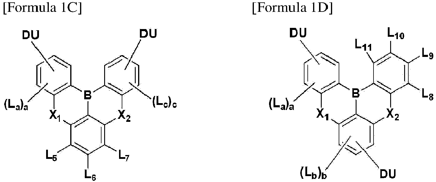
 a to c are each independently an integer from 0 to 3,X1 and X2 are the same as defined in Formula 1,La to Lc and L1 to L11 are each independently a hydrogen atom, a deuterium atom, a halogen atom, a cyano group, a substituted or unsubstituted amine group, a substituted or unsubstituted silyl group, a substituted or unsubstituted boron group, a substituted or unsubstituted linear or branched alkyl group having 1 to 20 carbon atoms, a substituted or unsubstituted aryl group having 6 to 30 ring-forming carbon atoms, or a substituted or unsubstituted heteroaryl group having 2 to 30 ring-forming carbon atoms, andDU is represented by Formula 2-a or Formula 2-b as defined in claim 1.
 - The organic electroluminescence device of claim 1, wherein Formula 1 is represented by Formula IF:
 R9 to R24 are the same as defined in Formula 2-b, andAU is a substituent represented by Formula 1, with the exception that AU is not substituted with a substituent represented by Formula 2-a or Formula 2-b.
 - The organic electroluminescence device of claim 1, wherein Formula 1 is represented by one of Formula 1F-1 to Formula 1F-3:


 L1 to L11 are each independently a hydrogen atom, a deuterium atom, a halogen atom, a cyano group, a substituted or unsubstituted amine group, a substituted or unsubstituted silyl group, a substituted or unsubstituted boron group, a substituted or unsubstituted linear or branched alkyl group having 1 to 20 carbon atoms, a substituted or unsubstituted aryl group having 6 to 30 ring-forming carbon atoms, or a substituted or unsubstituted heteroaryl group having 2 to 30 ring-forming carbon atoms,X1 and X2 are the same as defined in Formula 1, andR9 to R24 are the same as defined in Formula 2-b as defined in claim 1.
 - The organic electroluminescence device of claim 1, wherein
Ar1 and Ar2 are each independently an unsubstituted phenyl group, a phenyl group substituted with a deuterium atom, an unsubstituted biphenyl group, an unsubstituted naphthyl group, or an unsubstituted dibenzothiophene group. - The organic electroluminescence device of any one of claims 1 to 6, wherein
the organic electroluminescence device further includes a capping layer disposed on the second electrode, and
the capping layer has a refractive index of greater than or equal to about 1.6. - The organic electroluminescence device of any one of claims 1 to 7, wherein
the emission layer is a delayed fluorescence emission layer containing a host and a dopant, and
the dopant comprises the compound represented by Formula 1. - The organic electroluminescence device of any one of claims 1 to 8, wherein the emission layer emits light having a center wavelength in a range of about 430 nm to about 490 nm.
- The organic electroluminescence device of claim 1, wherein the emission layer comprises at least one of the compounds represented by Compound Group 1:


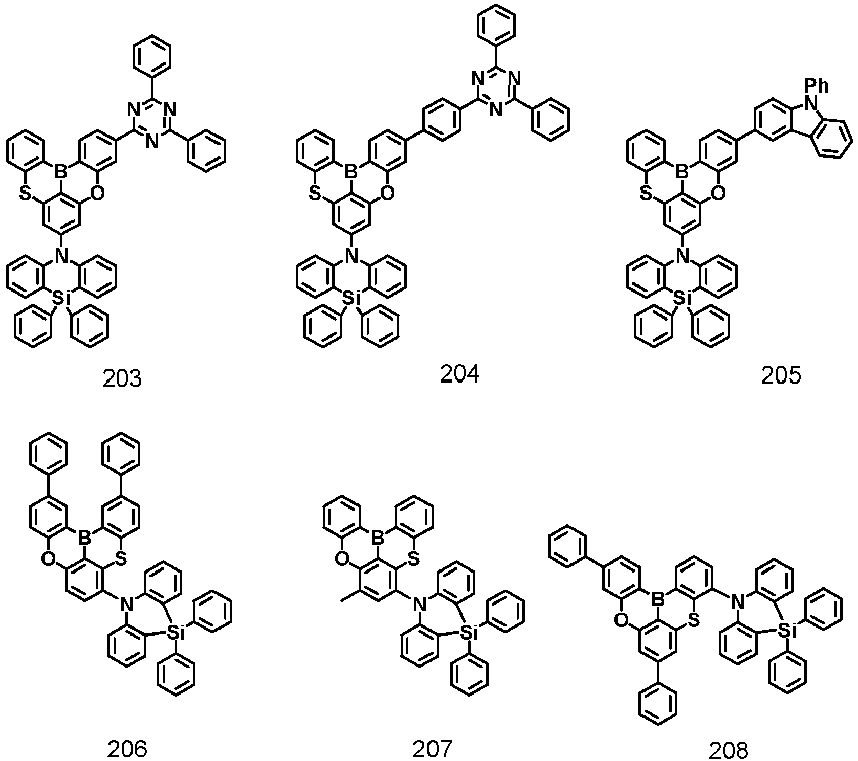

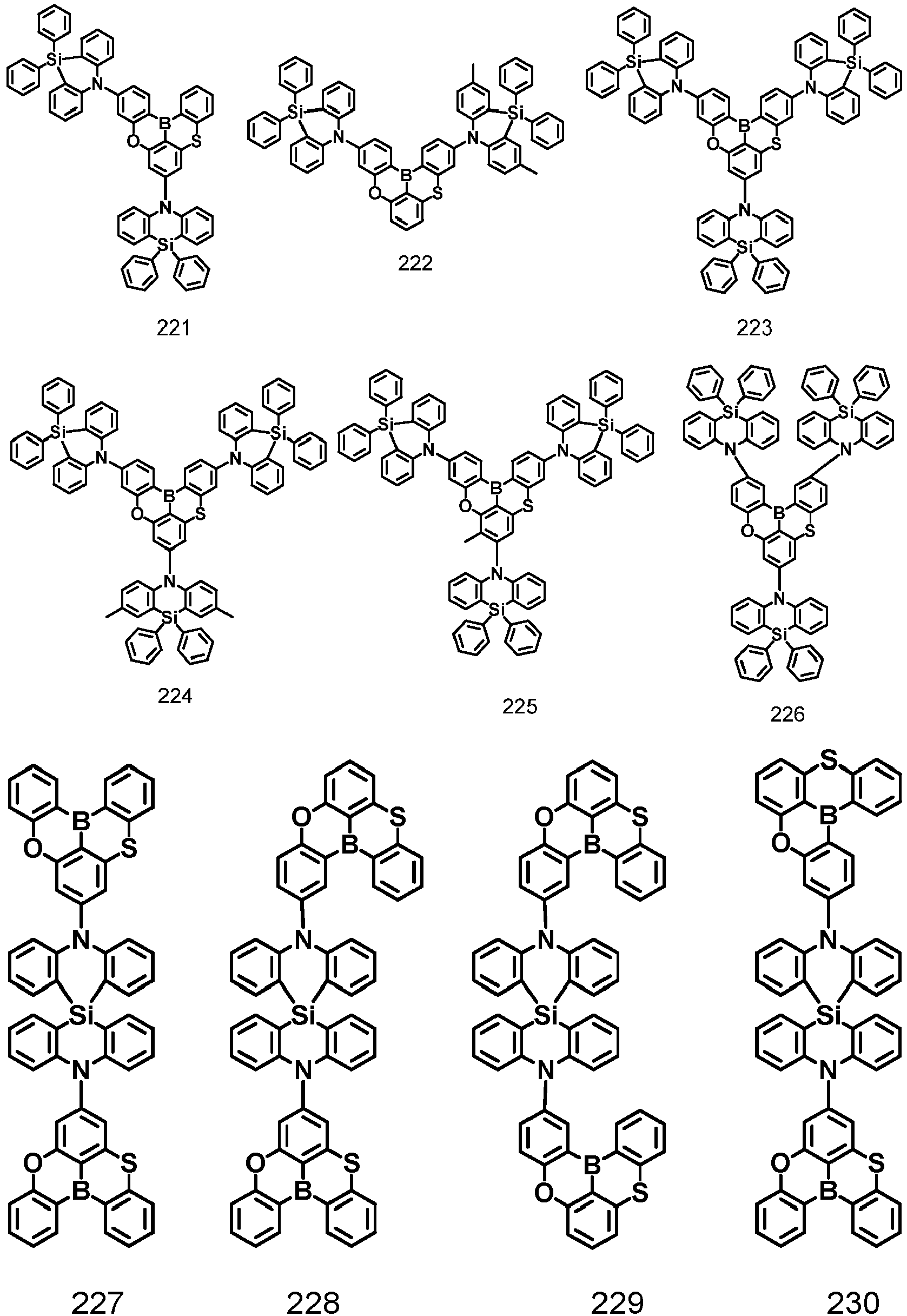

Applications Claiming Priority (1)
| Application Number | Priority Date | Filing Date | Title |
|---|---|---|---|
| KR1020200052327A KR102827472B1 (en) | 2020-04-29 | 2020-04-29 | Organic electroluminescence device and compound for organic electroluminescence device |
Publications (2)
| Publication Number | Publication Date |
|---|---|
| EP3905361A1 true EP3905361A1 (en) | 2021-11-03 |
| EP3905361B1 EP3905361B1 (en) | 2022-12-21 |
Family
ID=75728746
Family Applications (1)
| Application Number | Title | Priority Date | Filing Date |
|---|---|---|---|
| EP21171002.5A Active EP3905361B1 (en) | 2020-04-29 | 2021-04-28 | Organic electroluminescence device and compound for organic electroluminescence device |
Country Status (5)
| Country | Link |
|---|---|
| US (1) | US12178123B2 (en) |
| EP (1) | EP3905361B1 (en) |
| JP (1) | JP7805713B2 (en) |
| KR (1) | KR102827472B1 (en) |
| CN (1) | CN113563373A (en) |
Citations (2)
| Publication number | Priority date | Publication date | Assignee | Title |
|---|---|---|---|---|
| US20180019415A1 (en) * | 2016-07-13 | 2018-01-18 | Samsung Display Co., Ltd. | Polycyclic compound and organic electroluminescence device including the same |
| KR20200052327A (en) | 2017-09-04 | 2020-05-14 | 아게누스 인코포레이티드 | T cell receptor binding to mixed lineage leukemia (MLL) -specific phosphopeptides and methods of use thereof |
Family Cites Families (13)
| Publication number | Priority date | Publication date | Assignee | Title |
|---|---|---|---|---|
| KR100700013B1 (en) * | 2004-11-26 | 2007-03-26 | 삼성에스디아이 주식회사 | Organic electroluminescent device and manufacturing method thereof |
| US10374166B2 (en) * | 2014-02-18 | 2019-08-06 | Kwansei Gakuin Educational Foundation | Polycyclic aromatic compound |
| TWI636056B (en) | 2014-02-18 | 2018-09-21 | 學校法人關西學院 | Polycyclic aromatic compound and method for production the same, material for organic device and application thereof |
| JP6729589B2 (en) | 2015-07-24 | 2020-07-22 | コニカミノルタ株式会社 | Organic electroluminescence element, display device and lighting device |
| KR101876763B1 (en) | 2017-05-22 | 2018-07-11 | 머티어리얼사이언스 주식회사 | Organic compound and organic electroluminescent device comprising the same |
| KR102697986B1 (en) | 2018-04-05 | 2024-08-23 | 삼성디스플레이 주식회사 | Organic electroluminescence device and polycyclic compound for organic electroluminescence device |
| KR102260883B1 (en) * | 2018-07-19 | 2021-06-07 | 엘지디스플레이 주식회사 | Organic electroluminescent device |
| US12108659B2 (en) * | 2018-07-19 | 2024-10-01 | Lg Display Co., Ltd. | Organic electroluminescent device |
| KR102091507B1 (en) * | 2018-07-24 | 2020-03-20 | 머티어리얼사이언스 주식회사 | Organic electroluminescent device |
| CN108774258B (en) | 2018-09-10 | 2021-04-09 | 陕西蒲城海泰新材料产业有限责任公司 | Boron-containing heterocyclic compound and application thereof in organic photoelectric device |
| JP7595304B2 (en) * | 2019-04-26 | 2024-12-06 | 学校法人関西学院 | Compound, material for organic device, composition for forming light-emitting layer, organic field-effect transistor, organic thin-film solar cell, organic electroluminescent device, display device, and lighting device |
| KR102779449B1 (en) | 2019-06-21 | 2025-03-12 | 삼성디스플레이 주식회사 | Organic electroluminescence device and compound for organic electroluminescence device |
| KR102518765B1 (en) * | 2020-01-06 | 2023-04-06 | 경상국립대학교산학협력단 | Novel compound and organic light-emitting diode using them |
-
2020
- 2020-04-29 KR KR1020200052327A patent/KR102827472B1/en active Active
-
2021
- 2021-02-19 US US17/179,837 patent/US12178123B2/en active Active
- 2021-04-19 JP JP2021070640A patent/JP7805713B2/en active Active
- 2021-04-19 CN CN202110418986.4A patent/CN113563373A/en active Pending
- 2021-04-28 EP EP21171002.5A patent/EP3905361B1/en active Active
Patent Citations (2)
| Publication number | Priority date | Publication date | Assignee | Title |
|---|---|---|---|---|
| US20180019415A1 (en) * | 2016-07-13 | 2018-01-18 | Samsung Display Co., Ltd. | Polycyclic compound and organic electroluminescence device including the same |
| KR20200052327A (en) | 2017-09-04 | 2020-05-14 | 아게누스 인코포레이티드 | T cell receptor binding to mixed lineage leukemia (MLL) -specific phosphopeptides and methods of use thereof |
Non-Patent Citations (3)
| Title |
|---|
| GUOYUN MENG ET AL: "Isomeric Bright Sky-Blue TADF Emitters Based on BisacridineDecorated DBNA: Impact of Donor Locations on Luminescentand Electroluminescent Properties", ADV. OPTICAL MATER,, vol. 7, 25 March 2019 (2019-03-25), XP002800444, DOI: 10.1002/ADOM.201900130 * |
| HIROKI HIRAI ET AL: "One-Step Borylation of 1,3-Diaryloxybenzenes Towards Efficient Materials for Organic Light-Emitting Diodes", ANGEWANDTE CHEMIE INTERNATIONAL EDITION, vol. 54, no. 46, 18 September 2015 (2015-09-18), DE, pages 13581 - 13585, XP055310723, ISSN: 1433-7851, DOI: 10.1002/anie.201506335 * |
| SONG DONGDONG ET AL: "Asymmetric thermally activated delayed fluorescence (TADF) emitters with 5,9-dioxa-13 b -boranaphtho[3,2,1- de ]anthracene (OBA) as the acceptor and highly efficient blue-emitting OLEDs", JOURNAL OF MATERIALS CHEMISTRY C, vol. 7, no. 38, 3 September 2019 (2019-09-03), GB, pages 11953 - 11963, XP055838781, ISSN: 2050-7526, DOI: 10.1039/C9TC04115J * |
Also Published As
| Publication number | Publication date |
|---|---|
| US12178123B2 (en) | 2024-12-24 |
| JP7805713B2 (en) | 2026-01-26 |
| CN113563373A (en) | 2021-10-29 |
| KR102827472B1 (en) | 2025-07-02 |
| US20210351361A1 (en) | 2021-11-11 |
| EP3905361B1 (en) | 2022-12-21 |
| KR20210134116A (en) | 2021-11-09 |
| JP2021174990A (en) | 2021-11-01 |
Similar Documents
| Publication | Publication Date | Title |
|---|---|---|
| KR102858390B1 (en) | Organic electroluminescence device and polycyclic compound for organic electroluminescence device | |
| CN112194672B (en) | Organic electroluminescent devices and fused polycyclic compounds | |
| KR102785333B1 (en) | Organic electroluminescence device and fused polycyclic compound for organic electroluminescence device | |
| KR102770946B1 (en) | Organic electroluminescence device and polycyclic compound for organic electroluminescence device | |
| US11839150B2 (en) | Organic electroluminescence device and condensed cyclic compound for organic electroluminescence device | |
| US11276836B2 (en) | Organic electroluminescence device and polycyclic compound for organic electroluminescence device | |
| US11502259B2 (en) | Organic electroluminescence device and polycyclic compound for organic electroluminescence device | |
| KR102706953B1 (en) | Organic electroluminescence device and polycyclic compound for organic electroluminescence device | |
| US11515486B2 (en) | Organic electroluminescence device and polycyclic compound for organic electroluminescence device | |
| KR102567881B1 (en) | Compound including nitrogen and organic electroluminescence device including the same | |
| US12256633B2 (en) | Organic electroluminescence device and fused polycyclic compound for organic electroluminescence device | |
| KR102736371B1 (en) | Organic light-emitting compound and organic electroluminescent device using the same | |
| KR20210057263A (en) | Organic electroluminescence device and polycyclic compound for organic electroluminescence device | |
| KR102904115B1 (en) | Organic electroluminescence device and polycyclic compound for organic electroluminescence device | |
| JP7456757B2 (en) | Organic electroluminescent device and polycyclic compound for organic electroluminescent device | |
| JP7446793B2 (en) | Organic electroluminescent device and polycyclic compound for organic electroluminescent device | |
| KR102779449B1 (en) | Organic electroluminescence device and compound for organic electroluminescence device | |
| US12133456B2 (en) | Organic electroluminescence device and fused polycyclic compound for organic electroluminescence device | |
| KR102811543B1 (en) | Organic electroluminescence device and polycyclic compound for organic electroluminescence device | |
| EP3905361B1 (en) | Organic electroluminescence device and compound for organic electroluminescence device | |
| KR20210099678A (en) | Organic electroluminescence device and polycyclic compound for organic electroluminescence device | |
| KR102515592B1 (en) | Compound including nitrogen and organic electroluminescence device including the same | |
| KR20260074231A (en) | Organic light-emitting compound and organic electroluminescent device using the same | |
| KR20210050014A (en) | Organic electroluminescence device and compound for organic electroluminescence device |
Legal Events
| Date | Code | Title | Description |
|---|---|---|---|
| PUAI | Public reference made under article 153(3) epc to a published international application that has entered the european phase |
Free format text: ORIGINAL CODE: 0009012 |
|
| STAA | Information on the status of an ep patent application or granted ep patent |
Free format text: STATUS: THE APPLICATION HAS BEEN PUBLISHED |
|
| AK | Designated contracting states |
Kind code of ref document: A1 Designated state(s): AL AT BE BG CH CY CZ DE DK EE ES FI FR GB GR HR HU IE IS IT LI LT LU LV MC MK MT NL NO PL PT RO RS SE SI SK SM TR |
|
| B565 | Issuance of search results under rule 164(2) epc |
Effective date: 20210916 |
|
| STAA | Information on the status of an ep patent application or granted ep patent |
Free format text: STATUS: REQUEST FOR EXAMINATION WAS MADE |
|
| 17P | Request for examination filed |
Effective date: 20220317 |
|
| RBV | Designated contracting states (corrected) |
Designated state(s): AL AT BE BG CH CY CZ DE DK EE ES FI FR GB GR HR HU IE IS IT LI LT LU LV MC MK MT NL NO PL PT RO RS SE SI SK SM TR |
|
| GRAP | Despatch of communication of intention to grant a patent |
Free format text: ORIGINAL CODE: EPIDOSNIGR1 |
|
| STAA | Information on the status of an ep patent application or granted ep patent |
Free format text: STATUS: GRANT OF PATENT IS INTENDED |
|
| RIC1 | Information provided on ipc code assigned before grant |
Ipc: H01L 51/54 20060101AFI20220628BHEP |
|
| INTG | Intention to grant announced |
Effective date: 20220714 |
|
| GRAS | Grant fee paid |
Free format text: ORIGINAL CODE: EPIDOSNIGR3 |
|
| GRAA | (expected) grant |
Free format text: ORIGINAL CODE: 0009210 |
|
| STAA | Information on the status of an ep patent application or granted ep patent |
Free format text: STATUS: THE PATENT HAS BEEN GRANTED |
|
| REG | Reference to a national code |
Ref country code: DE Ref legal event code: R079 Ref document number: 602021001025 Country of ref document: DE Free format text: PREVIOUS MAIN CLASS: H01L0051540000 Ipc: H10K0085000000 |
|
| AK | Designated contracting states |
Kind code of ref document: B1 Designated state(s): AL AT BE BG CH CY CZ DE DK EE ES FI FR GB GR HR HU IE IS IT LI LT LU LV MC MK MT NL NO PL PT RO RS SE SI SK SM TR |
|
| REG | Reference to a national code |
Ref country code: GB Ref legal event code: FG4D |
|
| REG | Reference to a national code |
Ref country code: DE Ref legal event code: R096 Ref document number: 602021001025 Country of ref document: DE |
|
| REG | Reference to a national code |
Ref country code: CH Ref legal event code: EP |
|
| REG | Reference to a national code |
Ref country code: AT Ref legal event code: REF Ref document number: 1539587 Country of ref document: AT Kind code of ref document: T Effective date: 20230115 |
|
| REG | Reference to a national code |
Ref country code: IE Ref legal event code: FG4D |
|
| REG | Reference to a national code |
Ref country code: LT Ref legal event code: MG9D |
|
| REG | Reference to a national code |
Ref country code: NL Ref legal event code: MP Effective date: 20221221 |
|
| PG25 | Lapsed in a contracting state [announced via postgrant information from national office to epo] |
Ref country code: SE Free format text: LAPSE BECAUSE OF FAILURE TO SUBMIT A TRANSLATION OF THE DESCRIPTION OR TO PAY THE FEE WITHIN THE PRESCRIBED TIME-LIMIT Effective date: 20221221 Ref country code: NO Free format text: LAPSE BECAUSE OF FAILURE TO SUBMIT A TRANSLATION OF THE DESCRIPTION OR TO PAY THE FEE WITHIN THE PRESCRIBED TIME-LIMIT Effective date: 20230321 Ref country code: LT Free format text: LAPSE BECAUSE OF FAILURE TO SUBMIT A TRANSLATION OF THE DESCRIPTION OR TO PAY THE FEE WITHIN THE PRESCRIBED TIME-LIMIT Effective date: 20221221 Ref country code: FI Free format text: LAPSE BECAUSE OF FAILURE TO SUBMIT A TRANSLATION OF THE DESCRIPTION OR TO PAY THE FEE WITHIN THE PRESCRIBED TIME-LIMIT Effective date: 20221221 |
|
| REG | Reference to a national code |
Ref country code: AT Ref legal event code: MK05 Ref document number: 1539587 Country of ref document: AT Kind code of ref document: T Effective date: 20221221 |
|
| PG25 | Lapsed in a contracting state [announced via postgrant information from national office to epo] |
Ref country code: RS Free format text: LAPSE BECAUSE OF FAILURE TO SUBMIT A TRANSLATION OF THE DESCRIPTION OR TO PAY THE FEE WITHIN THE PRESCRIBED TIME-LIMIT Effective date: 20221221 Ref country code: LV Free format text: LAPSE BECAUSE OF FAILURE TO SUBMIT A TRANSLATION OF THE DESCRIPTION OR TO PAY THE FEE WITHIN THE PRESCRIBED TIME-LIMIT Effective date: 20221221 Ref country code: HR Free format text: LAPSE BECAUSE OF FAILURE TO SUBMIT A TRANSLATION OF THE DESCRIPTION OR TO PAY THE FEE WITHIN THE PRESCRIBED TIME-LIMIT Effective date: 20221221 Ref country code: GR Free format text: LAPSE BECAUSE OF FAILURE TO SUBMIT A TRANSLATION OF THE DESCRIPTION OR TO PAY THE FEE WITHIN THE PRESCRIBED TIME-LIMIT Effective date: 20230322 |
|
| PG25 | Lapsed in a contracting state [announced via postgrant information from national office to epo] |
Ref country code: NL Free format text: LAPSE BECAUSE OF FAILURE TO SUBMIT A TRANSLATION OF THE DESCRIPTION OR TO PAY THE FEE WITHIN THE PRESCRIBED TIME-LIMIT Effective date: 20221221 |
|
| P01 | Opt-out of the competence of the unified patent court (upc) registered |
Effective date: 20230530 |
|
| PG25 | Lapsed in a contracting state [announced via postgrant information from national office to epo] |
Ref country code: SM Free format text: LAPSE BECAUSE OF FAILURE TO SUBMIT A TRANSLATION OF THE DESCRIPTION OR TO PAY THE FEE WITHIN THE PRESCRIBED TIME-LIMIT Effective date: 20221221 Ref country code: RO Free format text: LAPSE BECAUSE OF FAILURE TO SUBMIT A TRANSLATION OF THE DESCRIPTION OR TO PAY THE FEE WITHIN THE PRESCRIBED TIME-LIMIT Effective date: 20221221 Ref country code: PT Free format text: LAPSE BECAUSE OF FAILURE TO SUBMIT A TRANSLATION OF THE DESCRIPTION OR TO PAY THE FEE WITHIN THE PRESCRIBED TIME-LIMIT Effective date: 20230421 Ref country code: ES Free format text: LAPSE BECAUSE OF FAILURE TO SUBMIT A TRANSLATION OF THE DESCRIPTION OR TO PAY THE FEE WITHIN THE PRESCRIBED TIME-LIMIT Effective date: 20221221 Ref country code: EE Free format text: LAPSE BECAUSE OF FAILURE TO SUBMIT A TRANSLATION OF THE DESCRIPTION OR TO PAY THE FEE WITHIN THE PRESCRIBED TIME-LIMIT Effective date: 20221221 Ref country code: CZ Free format text: LAPSE BECAUSE OF FAILURE TO SUBMIT A TRANSLATION OF THE DESCRIPTION OR TO PAY THE FEE WITHIN THE PRESCRIBED TIME-LIMIT Effective date: 20221221 Ref country code: AT Free format text: LAPSE BECAUSE OF FAILURE TO SUBMIT A TRANSLATION OF THE DESCRIPTION OR TO PAY THE FEE WITHIN THE PRESCRIBED TIME-LIMIT Effective date: 20221221 |
|
| PG25 | Lapsed in a contracting state [announced via postgrant information from national office to epo] |
Ref country code: SK Free format text: LAPSE BECAUSE OF FAILURE TO SUBMIT A TRANSLATION OF THE DESCRIPTION OR TO PAY THE FEE WITHIN THE PRESCRIBED TIME-LIMIT Effective date: 20221221 Ref country code: PL Free format text: LAPSE BECAUSE OF FAILURE TO SUBMIT A TRANSLATION OF THE DESCRIPTION OR TO PAY THE FEE WITHIN THE PRESCRIBED TIME-LIMIT Effective date: 20221221 Ref country code: IS Free format text: LAPSE BECAUSE OF FAILURE TO SUBMIT A TRANSLATION OF THE DESCRIPTION OR TO PAY THE FEE WITHIN THE PRESCRIBED TIME-LIMIT Effective date: 20230421 Ref country code: AL Free format text: LAPSE BECAUSE OF FAILURE TO SUBMIT A TRANSLATION OF THE DESCRIPTION OR TO PAY THE FEE WITHIN THE PRESCRIBED TIME-LIMIT Effective date: 20221221 |
|
| REG | Reference to a national code |
Ref country code: DE Ref legal event code: R097 Ref document number: 602021001025 Country of ref document: DE |
|
| PLBE | No opposition filed within time limit |
Free format text: ORIGINAL CODE: 0009261 |
|
| STAA | Information on the status of an ep patent application or granted ep patent |
Free format text: STATUS: NO OPPOSITION FILED WITHIN TIME LIMIT |
|
| PG25 | Lapsed in a contracting state [announced via postgrant information from national office to epo] |
Ref country code: DK Free format text: LAPSE BECAUSE OF FAILURE TO SUBMIT A TRANSLATION OF THE DESCRIPTION OR TO PAY THE FEE WITHIN THE PRESCRIBED TIME-LIMIT Effective date: 20221221 |
|
| 26N | No opposition filed |
Effective date: 20230922 |
|
| PG25 | Lapsed in a contracting state [announced via postgrant information from national office to epo] |
Ref country code: LU Free format text: LAPSE BECAUSE OF NON-PAYMENT OF DUE FEES Effective date: 20230428 |
|
| REG | Reference to a national code |
Ref country code: BE Ref legal event code: MM Effective date: 20230430 |
|
| PG25 | Lapsed in a contracting state [announced via postgrant information from national office to epo] |
Ref country code: MC Free format text: LAPSE BECAUSE OF FAILURE TO SUBMIT A TRANSLATION OF THE DESCRIPTION OR TO PAY THE FEE WITHIN THE PRESCRIBED TIME-LIMIT Effective date: 20221221 |
|
| PG25 | Lapsed in a contracting state [announced via postgrant information from national office to epo] |
Ref country code: SI Free format text: LAPSE BECAUSE OF FAILURE TO SUBMIT A TRANSLATION OF THE DESCRIPTION OR TO PAY THE FEE WITHIN THE PRESCRIBED TIME-LIMIT Effective date: 20221221 Ref country code: MC Free format text: LAPSE BECAUSE OF FAILURE TO SUBMIT A TRANSLATION OF THE DESCRIPTION OR TO PAY THE FEE WITHIN THE PRESCRIBED TIME-LIMIT Effective date: 20221221 |
|
| REG | Reference to a national code |
Ref country code: IE Ref legal event code: MM4A |
|
| PG25 | Lapsed in a contracting state [announced via postgrant information from national office to epo] |
Ref country code: BE Free format text: LAPSE BECAUSE OF NON-PAYMENT OF DUE FEES Effective date: 20230430 |
|
| PG25 | Lapsed in a contracting state [announced via postgrant information from national office to epo] |
Ref country code: IE Free format text: LAPSE BECAUSE OF NON-PAYMENT OF DUE FEES Effective date: 20230428 |
|
| PG25 | Lapsed in a contracting state [announced via postgrant information from national office to epo] |
Ref country code: IE Free format text: LAPSE BECAUSE OF NON-PAYMENT OF DUE FEES Effective date: 20230428 |
|
| PG25 | Lapsed in a contracting state [announced via postgrant information from national office to epo] |
Ref country code: IT Free format text: LAPSE BECAUSE OF FAILURE TO SUBMIT A TRANSLATION OF THE DESCRIPTION OR TO PAY THE FEE WITHIN THE PRESCRIBED TIME-LIMIT Effective date: 20221221 |
|
| PG25 | Lapsed in a contracting state [announced via postgrant information from national office to epo] |
Ref country code: BG Free format text: LAPSE BECAUSE OF FAILURE TO SUBMIT A TRANSLATION OF THE DESCRIPTION OR TO PAY THE FEE WITHIN THE PRESCRIBED TIME-LIMIT Effective date: 20221221 |
|
| PG25 | Lapsed in a contracting state [announced via postgrant information from national office to epo] |
Ref country code: BG Free format text: LAPSE BECAUSE OF FAILURE TO SUBMIT A TRANSLATION OF THE DESCRIPTION OR TO PAY THE FEE WITHIN THE PRESCRIBED TIME-LIMIT Effective date: 20221221 |
|
| REG | Reference to a national code |
Ref country code: CH Ref legal event code: PL |
|
| PG25 | Lapsed in a contracting state [announced via postgrant information from national office to epo] |
Ref country code: CH Free format text: LAPSE BECAUSE OF NON-PAYMENT OF DUE FEES Effective date: 20240430 |
|
| PGFP | Annual fee paid to national office [announced via postgrant information from national office to epo] |
Ref country code: DE Payment date: 20250320 Year of fee payment: 5 |
|
| PG25 | Lapsed in a contracting state [announced via postgrant information from national office to epo] |
Ref country code: CY Free format text: LAPSE BECAUSE OF FAILURE TO SUBMIT A TRANSLATION OF THE DESCRIPTION OR TO PAY THE FEE WITHIN THE PRESCRIBED TIME-LIMIT; INVALID AB INITIO Effective date: 20210428 |
|
| PG25 | Lapsed in a contracting state [announced via postgrant information from national office to epo] |
Ref country code: HU Free format text: LAPSE BECAUSE OF FAILURE TO SUBMIT A TRANSLATION OF THE DESCRIPTION OR TO PAY THE FEE WITHIN THE PRESCRIBED TIME-LIMIT; INVALID AB INITIO Effective date: 20210428 |
|
| PG25 | Lapsed in a contracting state [announced via postgrant information from national office to epo] |
Ref country code: TR Free format text: LAPSE BECAUSE OF FAILURE TO SUBMIT A TRANSLATION OF THE DESCRIPTION OR TO PAY THE FEE WITHIN THE PRESCRIBED TIME-LIMIT Effective date: 20221221 |
|
| PGFP | Annual fee paid to national office [announced via postgrant information from national office to epo] |
Ref country code: GB Payment date: 20260324 Year of fee payment: 6 |
|
| PGFP | Annual fee paid to national office [announced via postgrant information from national office to epo] |
Ref country code: FR Payment date: 20260323 Year of fee payment: 6 |