EP3905317A1 - Semiconductor device - Google Patents
Semiconductor device Download PDFInfo
- Publication number
- EP3905317A1 EP3905317A1 EP18944238.7A EP18944238A EP3905317A1 EP 3905317 A1 EP3905317 A1 EP 3905317A1 EP 18944238 A EP18944238 A EP 18944238A EP 3905317 A1 EP3905317 A1 EP 3905317A1
- Authority
- EP
- European Patent Office
- Prior art keywords
- semiconductor chip
- insulating film
- semiconductor
- light
- semiconductor device
- Prior art date
- Legal status (The legal status is an assumption and is not a legal conclusion. Google has not performed a legal analysis and makes no representation as to the accuracy of the status listed.)
- Granted
Links
Images


Classifications
-
- H—ELECTRICITY
- H10—SEMICONDUCTOR DEVICES; ELECTRIC SOLID-STATE DEVICES NOT OTHERWISE PROVIDED FOR
- H10W—GENERIC PACKAGES, INTERCONNECTIONS, CONNECTORS OR OTHER CONSTRUCTIONAL DETAILS OF DEVICES COVERED BY CLASS H10
- H10W74/00—Encapsulations, e.g. protective coatings
- H10W74/40—Encapsulations, e.g. protective coatings characterised by their materials
-
- H—ELECTRICITY
- H10—SEMICONDUCTOR DEVICES; ELECTRIC SOLID-STATE DEVICES NOT OTHERWISE PROVIDED FOR
- H10H—INORGANIC LIGHT-EMITTING SEMICONDUCTOR DEVICES HAVING POTENTIAL BARRIERS
- H10H20/00—Individual inorganic light-emitting semiconductor devices having potential barriers, e.g. light-emitting diodes [LED]
- H10H20/80—Constructional details
- H10H20/85—Packages
- H10H20/852—Encapsulations
-
- H—ELECTRICITY
- H10—SEMICONDUCTOR DEVICES; ELECTRIC SOLID-STATE DEVICES NOT OTHERWISE PROVIDED FOR
- H10H—INORGANIC LIGHT-EMITTING SEMICONDUCTOR DEVICES HAVING POTENTIAL BARRIERS
- H10H20/00—Individual inorganic light-emitting semiconductor devices having potential barriers, e.g. light-emitting diodes [LED]
- H10H20/80—Constructional details
- H10H20/85—Packages
- H10H20/8506—Containers
-
- H—ELECTRICITY
- H10—SEMICONDUCTOR DEVICES; ELECTRIC SOLID-STATE DEVICES NOT OTHERWISE PROVIDED FOR
- H10H—INORGANIC LIGHT-EMITTING SEMICONDUCTOR DEVICES HAVING POTENTIAL BARRIERS
- H10H20/00—Individual inorganic light-emitting semiconductor devices having potential barriers, e.g. light-emitting diodes [LED]
- H10H20/80—Constructional details
- H10H20/85—Packages
- H10H20/851—Wavelength conversion means
- H10H20/8511—Wavelength conversion means characterised by their material, e.g. binder
- H10H20/8512—Wavelength conversion materials
-
- H—ELECTRICITY
- H10—SEMICONDUCTOR DEVICES; ELECTRIC SOLID-STATE DEVICES NOT OTHERWISE PROVIDED FOR
- H10H—INORGANIC LIGHT-EMITTING SEMICONDUCTOR DEVICES HAVING POTENTIAL BARRIERS
- H10H20/00—Individual inorganic light-emitting semiconductor devices having potential barriers, e.g. light-emitting diodes [LED]
- H10H20/80—Constructional details
- H10H20/85—Packages
- H10H20/857—Interconnections, e.g. lead-frames, bond wires or solder balls
-
- H—ELECTRICITY
- H10—SEMICONDUCTOR DEVICES; ELECTRIC SOLID-STATE DEVICES NOT OTHERWISE PROVIDED FOR
- H10W—GENERIC PACKAGES, INTERCONNECTIONS, CONNECTORS OR OTHER CONSTRUCTIONAL DETAILS OF DEVICES COVERED BY CLASS H10
- H10W74/00—Encapsulations, e.g. protective coatings
- H10W74/10—Encapsulations, e.g. protective coatings characterised by their shape or disposition
-
- H—ELECTRICITY
- H10—SEMICONDUCTOR DEVICES; ELECTRIC SOLID-STATE DEVICES NOT OTHERWISE PROVIDED FOR
- H10H—INORGANIC LIGHT-EMITTING SEMICONDUCTOR DEVICES HAVING POTENTIAL BARRIERS
- H10H20/00—Individual inorganic light-emitting semiconductor devices having potential barriers, e.g. light-emitting diodes [LED]
- H10H20/80—Constructional details
- H10H20/85—Packages
- H10H20/851—Wavelength conversion means
-
- H—ELECTRICITY
- H10—SEMICONDUCTOR DEVICES; ELECTRIC SOLID-STATE DEVICES NOT OTHERWISE PROVIDED FOR
- H10W—GENERIC PACKAGES, INTERCONNECTIONS, CONNECTORS OR OTHER CONSTRUCTIONAL DETAILS OF DEVICES COVERED BY CLASS H10
- H10W72/00—Interconnections or connectors in packages
- H10W72/01—Manufacture or treatment
- H10W72/015—Manufacture or treatment of bond wires
- H10W72/01515—Forming coatings
-
- H—ELECTRICITY
- H10—SEMICONDUCTOR DEVICES; ELECTRIC SOLID-STATE DEVICES NOT OTHERWISE PROVIDED FOR
- H10W—GENERIC PACKAGES, INTERCONNECTIONS, CONNECTORS OR OTHER CONSTRUCTIONAL DETAILS OF DEVICES COVERED BY CLASS H10
- H10W72/00—Interconnections or connectors in packages
- H10W72/071—Connecting or disconnecting
- H10W72/073—Connecting or disconnecting of die-attach connectors
- H10W72/07351—Connecting or disconnecting of die-attach connectors characterised by changes in properties of the die-attach connectors during connecting
- H10W72/07352—Connecting or disconnecting of die-attach connectors characterised by changes in properties of the die-attach connectors during connecting changes in structures or sizes
-
- H—ELECTRICITY
- H10—SEMICONDUCTOR DEVICES; ELECTRIC SOLID-STATE DEVICES NOT OTHERWISE PROVIDED FOR
- H10W—GENERIC PACKAGES, INTERCONNECTIONS, CONNECTORS OR OTHER CONSTRUCTIONAL DETAILS OF DEVICES COVERED BY CLASS H10
- H10W72/00—Interconnections or connectors in packages
- H10W72/071—Connecting or disconnecting
- H10W72/075—Connecting or disconnecting of bond wires
-
- H—ELECTRICITY
- H10—SEMICONDUCTOR DEVICES; ELECTRIC SOLID-STATE DEVICES NOT OTHERWISE PROVIDED FOR
- H10W—GENERIC PACKAGES, INTERCONNECTIONS, CONNECTORS OR OTHER CONSTRUCTIONAL DETAILS OF DEVICES COVERED BY CLASS H10
- H10W72/00—Interconnections or connectors in packages
- H10W72/071—Connecting or disconnecting
- H10W72/075—Connecting or disconnecting of bond wires
- H10W72/07531—Techniques
- H10W72/07532—Compression bonding, e.g. thermocompression bonding
- H10W72/07533—Ultrasonic bonding, e.g. thermosonic bonding
-
- H—ELECTRICITY
- H10—SEMICONDUCTOR DEVICES; ELECTRIC SOLID-STATE DEVICES NOT OTHERWISE PROVIDED FOR
- H10W—GENERIC PACKAGES, INTERCONNECTIONS, CONNECTORS OR OTHER CONSTRUCTIONAL DETAILS OF DEVICES COVERED BY CLASS H10
- H10W72/00—Interconnections or connectors in packages
- H10W72/30—Die-attach connectors
- H10W72/321—Structures or relative sizes of die-attach connectors
-
- H—ELECTRICITY
- H10—SEMICONDUCTOR DEVICES; ELECTRIC SOLID-STATE DEVICES NOT OTHERWISE PROVIDED FOR
- H10W—GENERIC PACKAGES, INTERCONNECTIONS, CONNECTORS OR OTHER CONSTRUCTIONAL DETAILS OF DEVICES COVERED BY CLASS H10
- H10W72/00—Interconnections or connectors in packages
- H10W72/30—Die-attach connectors
- H10W72/351—Materials of die-attach connectors
- H10W72/352—Materials of die-attach connectors comprising metals or metalloids, e.g. solders
-
- H—ELECTRICITY
- H10—SEMICONDUCTOR DEVICES; ELECTRIC SOLID-STATE DEVICES NOT OTHERWISE PROVIDED FOR
- H10W—GENERIC PACKAGES, INTERCONNECTIONS, CONNECTORS OR OTHER CONSTRUCTIONAL DETAILS OF DEVICES COVERED BY CLASS H10
- H10W72/00—Interconnections or connectors in packages
- H10W72/50—Bond wires
- H10W72/551—Materials of bond wires
- H10W72/552—Materials of bond wires comprising metals or metalloids, e.g. silver
- H10W72/5524—Materials of bond wires comprising metals or metalloids, e.g. silver comprising aluminium [Al]
-
- H—ELECTRICITY
- H10—SEMICONDUCTOR DEVICES; ELECTRIC SOLID-STATE DEVICES NOT OTHERWISE PROVIDED FOR
- H10W—GENERIC PACKAGES, INTERCONNECTIONS, CONNECTORS OR OTHER CONSTRUCTIONAL DETAILS OF DEVICES COVERED BY CLASS H10
- H10W72/00—Interconnections or connectors in packages
- H10W72/50—Bond wires
- H10W72/59—Bond pads specially adapted therefor
-
- H—ELECTRICITY
- H10—SEMICONDUCTOR DEVICES; ELECTRIC SOLID-STATE DEVICES NOT OTHERWISE PROVIDED FOR
- H10W—GENERIC PACKAGES, INTERCONNECTIONS, CONNECTORS OR OTHER CONSTRUCTIONAL DETAILS OF DEVICES COVERED BY CLASS H10
- H10W72/00—Interconnections or connectors in packages
- H10W72/851—Dispositions of multiple connectors or interconnections
- H10W72/874—On different surfaces
- H10W72/884—Die-attach connectors and bond wires
-
- H—ELECTRICITY
- H10—SEMICONDUCTOR DEVICES; ELECTRIC SOLID-STATE DEVICES NOT OTHERWISE PROVIDED FOR
- H10W—GENERIC PACKAGES, INTERCONNECTIONS, CONNECTORS OR OTHER CONSTRUCTIONAL DETAILS OF DEVICES COVERED BY CLASS H10
- H10W72/00—Interconnections or connectors in packages
- H10W72/90—Bond pads, in general
- H10W72/941—Dispositions of bond pads
- H10W72/944—Dispositions of multiple bond pads
-
- H—ELECTRICITY
- H10—SEMICONDUCTOR DEVICES; ELECTRIC SOLID-STATE DEVICES NOT OTHERWISE PROVIDED FOR
- H10W—GENERIC PACKAGES, INTERCONNECTIONS, CONNECTORS OR OTHER CONSTRUCTIONAL DETAILS OF DEVICES COVERED BY CLASS H10
- H10W74/00—Encapsulations, e.g. protective coatings
-
- H—ELECTRICITY
- H10—SEMICONDUCTOR DEVICES; ELECTRIC SOLID-STATE DEVICES NOT OTHERWISE PROVIDED FOR
- H10W—GENERIC PACKAGES, INTERCONNECTIONS, CONNECTORS OR OTHER CONSTRUCTIONAL DETAILS OF DEVICES COVERED BY CLASS H10
- H10W90/00—Package configurations
- H10W90/701—Package configurations characterised by the relative positions of pads or connectors relative to package parts
- H10W90/731—Package configurations characterised by the relative positions of pads or connectors relative to package parts of die-attach connectors
- H10W90/734—Package configurations characterised by the relative positions of pads or connectors relative to package parts of die-attach connectors between a chip and a stacked insulating package substrate, interposer or RDL
-
- H—ELECTRICITY
- H10—SEMICONDUCTOR DEVICES; ELECTRIC SOLID-STATE DEVICES NOT OTHERWISE PROVIDED FOR
- H10W—GENERIC PACKAGES, INTERCONNECTIONS, CONNECTORS OR OTHER CONSTRUCTIONAL DETAILS OF DEVICES COVERED BY CLASS H10
- H10W90/00—Package configurations
- H10W90/701—Package configurations characterised by the relative positions of pads or connectors relative to package parts
- H10W90/751—Package configurations characterised by the relative positions of pads or connectors relative to package parts of bond wires
- H10W90/754—Package configurations characterised by the relative positions of pads or connectors relative to package parts of bond wires between a chip and a stacked insulating package substrate, interposer or RDL
Definitions
- the present invention relates to a semiconductor device having a resin-sealed packaged structure in which a semiconductor chip is sealed with resin.
- Semiconductor chips serving as transistors and diodes have the characteristics that are influenced by dirt or static electricity on the surface.
- a thin metallic wire connecting electrodes arranged on the surface of a semiconductor chip does not have resistance to oscillation when exposed directly on the surface.
- the semiconductor chip and the circumference thereof are thus typically filled and sealed mainly with resin insulating material, as disclosed in Patent Literature 1, for example.
- a band gap of a silicon (Si) semiconductor is 1.12 eV
- a band gap of a gallium arsenide (GaAs) semiconductor is 1.43 eV.
- the shortest wavelengths of light emitted from the respective semiconductors are 1,107 nm and 867 nm, which are both infrared light. The heat is thus only generated if the sealing resin is irradiated with the generated light.
- a band gap of a silicon carbide (SiC) semiconductor is 3.26 eV in the case of 4H type, and a band gap of a gallium nitride (GaN) semiconductor is 3.39 eV, which have been increasingly used as a next-generation semiconductor.
- the shortest wavelengths of light generated in the respective wide band-gap semiconductors are 380 nm and 366 nm, which are both ultraviolet light exceeding a range of visible light.
- the ultraviolet light of this type is able to cut out particular molecular bonding of resin, the various properties can be presumed to be deteriorated on a long-term basis depending on the type of resin used for sealing the semiconductor chip.
- a light-emitting device using a light-emitting diode (LED) as a light source including a wide band-gap semiconductor for example, a measure has been proposed that converts the ultraviolet light to visible light by use of a fluorescent substance, and further avoids the deterioration of the sealing resin caused by the ultraviolet light not converted (refer to Patent Literature 2).
- a power semiconductor device using a wide band-gap semiconductor is conventionally packaged by resin sealing while not taking account of the above problem of the ultraviolet light.
- the reason for this is that a transistor intended to be put to practical use in the SiC semiconductor or the GaN semiconductor is a unipolar device such as a MOSFET, and a forward current does not flow through the internal p-n junction in a normal operation, which causes no ultraviolet light.
- the present invention provides a semiconductor device having a packaged structure capable of preventing deterioration of a sealing resin caused by light generated in a p-n junction of a semiconductor chip so as to ensure a long-term reliability.
- a semiconductor device includes a functional region arranged between a semiconductor chip and a sealing resin and configured to prevent a light from reaching the sealing resin, the light being generated in a p-n junction of the semiconductor chip and having a wavelength causing deterioration of the sealing resin.
- the present invention can provide a semiconductor device having a packaged structure capable of preventing deterioration of a sealing resin caused by a light generated in a p-n junction of a semiconductor chip so as to ensure a long-term reliability.
- Fig. 1 is a schematic cross-sectional view illustrating a semiconductor device according to a first embodiment of the present invention.
- Reference numeral 1 shown in the drawings indicates a semiconductor chip including a wide band-gap semiconductor such as SiC or GaN particularly having a wide band gap that corresponds to a wavelength of light corresponding to ultraviolet light.
- the first embodiment is illustrated with a case in which the semiconductor chip 1 is a vertical p-n diode chip. It should be understood that the present invention can achieve the similar effects also in a case of using a semiconductor chip such as a MOSFET, a bipolar transistor, and an IGBT.
- the semiconductor chip 1 is provided with a p-n junction 13 such that a semiconductor region 12 of p-type is deposited on the surface of a semiconductor region 11 of n-type serving as a base body.
- the semiconductor chip 1 also includes a first main electrode 101 on the rear surface serving as a cathode.
- the semiconductor chip 1 further includes a second main electrode 102 on the front surface serving as an anode connected to the p-type semiconductor region 12. While the n-type semiconductor region 11 actually includes a high-concentration region occupying the most part and a low-concentration region arranged in layers only adjacent to the p-type semiconductor region 12, the respective drawings simply illustrate the semiconductor region 11 without being defined by the respective regions for illustration purposes.
- the semiconductor chip 1 is packaged on a metallic wiring layer provided on a substrate 40 having an insulating property.
- a first wiring pattern 41 illustrated in Fig. 1 is a cathode wiring layer arranged on the top surface of the substrate 40.
- the first main electrode 101 provided on the main surface of the semiconductor chip 1 opposed to the top surface of the substrate 40 is electrically and physically connected to the first wiring pattern 41 via a bonding member 50 made of metal by soldering, for example.
- the second main electrode 102 is electrically connected to a second wiring pattern 42 provided on the substrate 40 separately from the first wiring pattern 41 via a metal wire 60.
- the metal wire 60 is made of an alloy mainly including aluminum, for example, and is bonded to the surface of the metal included in the second main electrode 102 and the surface of the metal included in the second wiring pattern 42 principally by ultrasonic bonding.
- the packaged structure as described above is covered with a sealing resin 30 as illustrated in Fig. 1 so as to avoid deterioration in performance of the semiconductor chip 1 caused by external dirt, and ensure oscillation resistance of the metal wire 60.
- the sealing resin 30 used typically is a black-colored opaque epoxy resin, for example.
- the packaged structure illustrated in Fig. 1 further includes a functional insulating film 20 between the semiconductor chip 1 and the sealing resin 30.
- the functional insulating film 20 is a form of the element referred to above as the "functional region" in "SOLUTION TO PROBLEM" of the present specification.
- the functional insulating film 20 that is a kind of the "functional region” described above has the function of suppressing damage to the molecular bonding.
- the functional insulating film 20 used herein is made of a resin including a fluorescent substance, for example.
- the fluorescent substance has the properties that, when receiving a light having a short wavelength, converts part of the energy into heat and emits a light having a long wavelength.
- the fluorescent substance included in the functional insulating film 20 is thus chosen from material that converts the ultraviolet light generated in the p-n junction 13 in the semiconductor chip 1 into a light harmless to the sealing resin 30 such as visible light.
- the fluorescent substance of this type is a material used for implementing a LED that emits red, green, and yellow lights by use of an ultraviolet LED or a blue LED, or used when combining plural fluorescent substances to emit light having a plurality of wavelengths to implement a white LED device (refer to Non-Patent Literature 1).
- a base body of the functional insulating film 20 is made of material chosen from organic material having resistance to the generated light and suitably used for covering the entire semiconductor chip 1 deposited on the substrate 40 as illustrated in Fig. 1 .
- the material is chosen from aromatic polyimide that can be formed into a uniform film by spraying as illustrated in Fig. 1 , and hardly reacts to the ultraviolet light generated in the p-n junction 13.
- ultraviolet-curable resin that causes a polymerization reaction by irradiation with ultraviolet light can be used as the base body of the functional insulating film 20, since the ultraviolet-curable resin does not result in serious deterioration if continuously irradiated with the ultraviolet light after the completion of the polymerization, as compared with other types of resin.
- heat-resistant silicone can also be used as the base body of the functional insulating film 20, since bonding energy of the molecular bonding associated with silicon is typically higher than that associated with carbon.
- a film thickness of the functional insulating film 20 is set to be sufficiently greater than the wavelength of the generated light.
- the film thickness is preferably set to be at least several times as large as the wavelength.
- the semiconductor device according to the first embodiment of the present invention includes the functional insulating film 20 arranged between the semiconductor chip 1 and the sealing resin 30 so as to prevent the light having a particular wavelength and causing the deterioration of the sealing resin 30 from reaching the sealing resin 30.
- the semiconductor device as illustrated in Fig. 1 thus can avoid or reduce the deterioration of the sealing resin 30 regardless of whether the semiconductor chip 1 including the wide band-gap semiconductor internally emits the ultraviolet light during its operation, for example. This can extend the life span of the semiconductor device in which the semiconductor chip 1 including the wide band-gap semiconductor is packaged to a preferred period of time, while using the conventionally-used resin as the sealing resin 30 that exhibits sufficient performance in various aspects and has the advantage of reducing costs.
- Fig. 1 illustrates the semiconductor device with the case of including the functional insulating film 20 having a substantially uniform thickness and arranged on the top and the side surfaces of the semiconductor chip
- the functional insulating film 20 is not limited to the configuration as illustrated in Fig. 1 .
- the functional insulating film 20 may be arranged into a liquid-drop state potted on the top surface of the substrate 40 (the same is also applied to the following modified examples).
- FIG. 3 illustrates the functional insulating film 20 including a large amount of microcrystal particles 210 composed of a conductor having the same band gap as or a narrower band gap than the semiconductor composing the semiconductor chip 1.
- the microcrystal particles 210 include a large amount of crystal defects, which form various levels in the band gap. When the generated light enters the microcrystal particles 210, a light having a longer wavelength is emitted, as in the case of the fluorescent substance described above.
- the functional insulating film 20 including a large amount of the microcrystal particles 210 thus has the same function as the fluorescent substance.
- a constituent substance of the microcrystal particles 210 can be the same as that of the semiconductor chip 1. Alternatively, a material having a narrower band gap, such as microcrystals of Si inexpensive and easily available, may be used.
- a diameter of the microcrystal particles 210 is preferably set to be sufficiently greater than the wavelength of the light emitted from the semiconductor chip 1.
- a density of the microcrystal particles 210 in the functional insulating film 20 is designed so as not to allow the generated light to directly pass through the functional insulating film 20 without hitting the microcrystal particles 210.
- the microcrystal particles 210 are preferably formed in multiple layers in the functional insulating film 20, as illustrated in Fig. 3 .
- the functional insulating film 20 including the microcrystal particles 210 can also achieve the same effects as described above with reference to Fig. 1 .
- the configuration illustrated in Fig. 3 does not necessarily include the fluorescent substance, and can make use of the microcrystal particles composed of the semiconductor of the same type as the semiconductor chip 1 or the inexpensive microcrystal particles such as Si.
- the functional insulating film 20 can include the same fluorescent substance as illustrated in Fig. 1 with no limitation.
- Resin typically has a greater coefficient of thermal expansion than a semiconductor.
- Using the microcrystal particles 210 including the semiconductor in the sealing resin 30 can relax thermal stress caused between the semiconductor chip 1 and the functional insulating film 20 because of a change in temperature during use.
- the configuration illustrated in Fig. 3 is also suitably used so as to avoid damage caused by the thermal stress.
- Fig. 4 is a cross-sectional view similar to Fig. 1 .
- the functional insulating film 20 illustrated in Fig. 4 includes reflective particles 20 including a substance at least on the surface that reflects the ultraviolet light emitted from the semiconductor chip 1.
- a density of the reflective particles 220 in the functional insulating film 20 is also designed to be formed at least in multiple layers in the functional insulating film 20 as illustrated in Fig. 4 so as not to allow the light generated in the semiconductor chip 1 to directly pass through the functional insulating film 20 without hitting the reflective particles 220, as in the case illustrated in Fig. 3 .
- a constituent substance of the reflective particles 220 to be used is preferably zinc oxide or titanium oxide, for example. Since these substances have electrical conductivity, an insulating component of the functional insulating film 20 should be interposed between the respective reflective particles 220.
- a particle diameter and a deposited thickness of the reflective particles 220 are designed so as not to allow the generated light to reach the sealing resin 30, as in the case of the first modified example.
- the particle diameter of the reflective particles 220 is preferably set to be greater than the wavelength of the generated light.
- the functional insulating film 20 including the reflective particles 220 that reflect the generated light can also achieve the effect of not allowing the generated light to reach the sealing resin 30.
- the functional insulating film 20 including the reflective particles 220 also may further include the fluorescent substance.
- FIG. 5 is a partly-enlarged cross-sectional view of the functional insulating film 20 adjacent to the semiconductor chip 1.
- the functional insulating film 20 illustrated in Fig. 5 includes fluorescent microparticles 230, each including a particulate base body 232 having a substantially spherical shape, and a fluorescent layer 231 covering the surface of the particulate base body 232.
- the particulate base body 232 is made of a material having a higher refractive index than the functional insulating film 20. Choosing such a material for the particulate base body 232 causes the generated light L entering the surface of the respective fluorescent microparticles 230 at a shallow angle to advance in the fluorescent layer 231 including the fluorescent substance while being repeatedly refracted at the interfaces.
- the functional insulating film 20 including the fluorescent microparticles 230 can efficiently convert the wavelength of the generated light L.
- the particulate base body 232 thus preferably has the substantially spherical shape, instead of a shape provided with an acute angle part.
- the particulate base body 232 may be made of any material that can suppress great deterioration when absorbing the generated light L.
- the particulate base body 232 may be made of the same material as the microcrystal particles 210 and the reflective particles 220, or may be made of a different material.
- the fluorescent layer 231 preferably has a thickness set to be greater than the wavelength of the generated light L.
- the material included in the particulate base body 232 is preferably a substance having a small coefficient of thermal expansion, such as quartz glass having a low thermal-expansion coefficient, which is conventionally mixed in a sealing resin of a power semiconductor package, for example.
- the configuration as described above can provide the functional region while using a lower-priced material than the microcrystal particles 210 as described with reference to Fig. 3 .
- FIG. 6 is a cross-sectional view of a semiconductor device similar to that illustrated in Fig. 1 .
- the semiconductor device of this embodiment differs from that of the above embodiment in that the bonding member 50 further extends between the side surface of the semiconductor chip 1 and the functional insulating film 20.
- the bonding member 50 includes a ZnAl material
- Zn in the solid ZnAl material when melted evaporates at a melding point or higher to turn into vapor, and adheres to the side surface of the semiconductor chip 1.
- the molten ZnAl material comes up along the side surface of the semiconductor chip 1 and is then solidified.
- a metal film of the ZnAl material included in the bonding member 50 is thus formed on the side surface of the semiconductor chip 1 as illustrated in Fig. 6 , so as to have a function of reflecting the generated light.
- Fig. 7 is an enlarged cross-sectional view illustrating only the part adjacent to the left side surface of the semiconductor chip 1 illustrated in Fig. 1 .
- Fig. 7 omits the illustration of the other elements including the sealing resin 30.
- the mark " ⁇ " indicates a polycrystal region 15 formed in an inactive region adjacent to the side wall of the semiconductor chip 1.
- the term "inactive region” as used herein refers to a region not serving as a current path during the operation of the semiconductor chip 1, and a region having no influence on a breakdown voltage upon reverse bias of the semiconductor chip 1. In particular, the region is located at the circumference of the side wall of the semiconductor chip 1.
- the polycrystal region 15 can be formed by use of a convergent pulse laser typically used for a laser stealth dicing method.
- the use of the convergent pulse laser can form the polycrystal region locally at an optional position in the semiconductor (refer to Non-Patent Literature 2).
- the object of the laser stealth dicing is to form a number of belt-like defect regions by this method so as to divide the semiconductor chip into parts with a relatively light external force.
- the present embodiment uses this method to locally form, in the semiconductor chip 1, crystal defect regions having the same function as the fluorescent substance, as in the case of the microcrystal particles 210 described with reference to Fig. 3 .
- Reducing the laser output and forming multiple layers by local radiation at appropriate intervals can form a region that converts the ultraviolet light emitted from the inside of the semiconductor chip 1 into a harmless light while avoiding unintended deterioration in mechanical strength.
- the provision of the polycrystal region 15 in the semiconductor chip 1 can eliminate the functional insulating film 20 or can serve as a part of the function thereof, so as to ensure the effect of suppressing the deterioration of the sealing resin more easily.
- the present invention can also be effectively applied to a packaged structure of a MOSFET, a JFET, a bipolar transistor, an IGBT, or a thyristor that includes a p-n junction and allows a forward current to flow therethrough.
- the semiconductor device according to the present invention can be used in electronics industries including manufacturing industries for manufacturing semiconductor devices having a resin-sealed packaged structure in which a semiconductor chip is sealed with resin.
Landscapes
- Structures Or Materials For Encapsulating Or Coating Semiconductor Devices Or Solid State Devices (AREA)
- Led Device Packages (AREA)
Abstract
Description
- The present invention relates to a semiconductor device having a resin-sealed packaged structure in which a semiconductor chip is sealed with resin.
- Semiconductor chips serving as transistors and diodes have the characteristics that are influenced by dirt or static electricity on the surface. A thin metallic wire connecting electrodes arranged on the surface of a semiconductor chip does not have resistance to oscillation when exposed directly on the surface. The semiconductor chip and the circumference thereof are thus typically filled and sealed mainly with resin insulating material, as disclosed in
Patent Literature 1, for example. -
- Patent Literature 1:
Japanese Unexamined Patent Application Publication No. 2013-062540 - Patent Literature 2:
Japanese Unexamined Patent Application Publication No. 2009-099784 -
- Non-Patent Literature 1: TAGUCHI Tsunemasa, "The 21st Century Lighting Based on White Light-Emitting Diodes (LEDs)"; Journal of the Illuminating Engineering Institute of Japan, 2001, volume 85, No. 7, p. 496-501
- Non-Patent Literature 2: UCHIYAMA Naoki, "Complete Dry Process Laser Dicing"; Journal of the Japan Society of Precision Engineering, 2010, volume 76, No. 7, p. 747-750
- When a forward current flows through a p-n junction in the semiconductor chip, light having energy corresponding to a band gap of a semiconductor implementing the p-n junction is theoretically generated regardless of a direct band gap type or an indirect band gap type. A band gap of a silicon (Si) semiconductor is 1.12 eV, and a band gap of a gallium arsenide (GaAs) semiconductor is 1.43 eV. The shortest wavelengths of light emitted from the respective semiconductors are 1,107 nm and 867 nm, which are both infrared light. The heat is thus only generated if the sealing resin is irradiated with the generated light.
- A band gap of a silicon carbide (SiC) semiconductor is 3.26 eV in the case of 4H type, and a band gap of a gallium nitride (GaN) semiconductor is 3.39 eV, which have been increasingly used as a next-generation semiconductor. The shortest wavelengths of light generated in the respective wide band-gap semiconductors are 380 nm and 366 nm, which are both ultraviolet light exceeding a range of visible light.
- Since the ultraviolet light of this type is able to cut out particular molecular bonding of resin, the various properties can be presumed to be deteriorated on a long-term basis depending on the type of resin used for sealing the semiconductor chip. With regard to a light-emitting device using a light-emitting diode (LED) as a light source including a wide band-gap semiconductor, for example, a measure has been proposed that converts the ultraviolet light to visible light by use of a fluorescent substance, and further avoids the deterioration of the sealing resin caused by the ultraviolet light not converted (refer to Patent Literature 2).
- A power semiconductor device using a wide band-gap semiconductor is conventionally packaged by resin sealing while not taking account of the above problem of the ultraviolet light. The reason for this is that a transistor intended to be put to practical use in the SiC semiconductor or the GaN semiconductor is a unipolar device such as a MOSFET, and a forward current does not flow through the internal p-n junction in a normal operation, which causes no ultraviolet light.
- However, the inventors found out that a forward current flows in a parasitic p-n diode present in such a unipolar device depending on a driving means, and ultraviolet light is thus frequently generated. A packaged structure using a sealing resin designed without taking account of this problem could be deteriorated sightly earlier than expected in terms of the properties such as adhesiveness between the semiconductor chip and the sealing resin due to the generated ultraviolet light. A bipolar device such as an IGBT using a wide band-gap semiconductor, which has been studied so as to be put to practical use in the hear future, also has the same problem since ultraviolet light is generated during the original operation. Further, since the sealing resin in the packaged structure of the power semiconductor is opaque to the ultraviolet light, which is different from the packaged structure of the LED, the ultraviolet light generated all has the influence on the molecular bonding of the sealing resin.
- In view of the foregoing problems, the present invention provides a semiconductor device having a packaged structure capable of preventing deterioration of a sealing resin caused by light generated in a p-n junction of a semiconductor chip so as to ensure a long-term reliability.
- A semiconductor device according to an aspect of the present invention includes a functional region arranged between a semiconductor chip and a sealing resin and configured to prevent a light from reaching the sealing resin, the light being generated in a p-n junction of the semiconductor chip and having a wavelength causing deterioration of the sealing resin.
- The present invention can provide a semiconductor device having a packaged structure capable of preventing deterioration of a sealing resin caused by a light generated in a p-n junction of a semiconductor chip so as to ensure a long-term reliability.
-
- [
Fig. 1] Fig. 1 is a schematic cross-sectional view illustrating a structure of a semiconductor device according to a first embodiment of the present invention. - [
Fig. 2] Fig. 2 is a schematic cross-sectional view illustrating another structure of the semiconductor device according to the first embodiment of the present invention. - [
Fig. 3] Fig. 3 is a schematic cross-sectional view illustrating a structure of a semiconductor device according to a first modified example of the first embodiment of the present invention. - [
Fig. 4] Fig. 4 is a schematic cross-sectional view illustrating a structure of a semiconductor device according to a second modified example of the first embodiment of the present invention. - [
Fig. 5] Fig. 5 is a schematic cross-sectional view illustrating a structure of a semiconductor device according to a third modified example of the first embodiment of the present invention. - [
Fig. 6] Fig. 6 is a schematic cross-sectional view illustrating a structure of a semiconductor device according to a second embodiment of the present invention. - [
Fig. 7] Fig. 7 is a schematic cross-sectional view illustrating a structure of a semiconductor device according to a third embodiment of the present invention. - Hereinafter, embodiments according to the present invention are described with reference to the drawings. The same or similar elements illustrated in the drawings are denoted by the same or similar reference numerals. It should be understood that the drawings are illustrated schematically, and the respective dimensions and vertical and lateral proportions in the drawings are not drawn to scale. It should also be understood that the dimensional relationships and proportions between the respective drawings can differ from each other.
-
Fig. 1 is a schematic cross-sectional view illustrating a semiconductor device according to a first embodiment of the present invention.Reference numeral 1 shown in the drawings indicates a semiconductor chip including a wide band-gap semiconductor such as SiC or GaN particularly having a wide band gap that corresponds to a wavelength of light corresponding to ultraviolet light. To simplify the explanations of the present invention, the first embodiment is illustrated with a case in which thesemiconductor chip 1 is a vertical p-n diode chip. It should be understood that the present invention can achieve the similar effects also in a case of using a semiconductor chip such as a MOSFET, a bipolar transistor, and an IGBT. Thesemiconductor chip 1 is provided with ap-n junction 13 such that asemiconductor region 12 of p-type is deposited on the surface of asemiconductor region 11 of n-type serving as a base body. Thesemiconductor chip 1 also includes a firstmain electrode 101 on the rear surface serving as a cathode. Thesemiconductor chip 1 further includes a secondmain electrode 102 on the front surface serving as an anode connected to the p-type semiconductor region 12. While the n-type semiconductor region 11 actually includes a high-concentration region occupying the most part and a low-concentration region arranged in layers only adjacent to the p-type semiconductor region 12, the respective drawings simply illustrate thesemiconductor region 11 without being defined by the respective regions for illustration purposes. - The
semiconductor chip 1 is packaged on a metallic wiring layer provided on asubstrate 40 having an insulating property. Afirst wiring pattern 41 illustrated inFig. 1 is a cathode wiring layer arranged on the top surface of thesubstrate 40. The firstmain electrode 101 provided on the main surface of thesemiconductor chip 1 opposed to the top surface of thesubstrate 40 is electrically and physically connected to thefirst wiring pattern 41 via a bondingmember 50 made of metal by soldering, for example. The secondmain electrode 102 is electrically connected to asecond wiring pattern 42 provided on thesubstrate 40 separately from thefirst wiring pattern 41 via ametal wire 60. Themetal wire 60 is made of an alloy mainly including aluminum, for example, and is bonded to the surface of the metal included in the secondmain electrode 102 and the surface of the metal included in thesecond wiring pattern 42 principally by ultrasonic bonding. - The packaged structure as described above is covered with a
sealing resin 30 as illustrated inFig. 1 so as to avoid deterioration in performance of thesemiconductor chip 1 caused by external dirt, and ensure oscillation resistance of themetal wire 60. The sealingresin 30 used typically is a black-colored opaque epoxy resin, for example. The packaged structure illustrated inFig. 1 further includes a functionalinsulating film 20 between thesemiconductor chip 1 and thesealing resin 30. The functionalinsulating film 20 is a form of the element referred to above as the "functional region" in "SOLUTION TO PROBLEM" of the present specification. When a forward current flows in thep-n junction 13 in thesemiconductor chip 1 including the wide band-gap semiconductor, ultraviolet light, which is able to cut out the molecular bonding of an organic compound composing thesealing resin 30, is generated (referred to below as "generated light"). The functionalinsulating film 20 that is a kind of the "functional region" described above has the function of suppressing damage to the molecular bonding. - The function of the functional insulating
film 20 is described below. - The functional insulating
film 20 used herein is made of a resin including a fluorescent substance, for example. The fluorescent substance has the properties that, when receiving a light having a short wavelength, converts part of the energy into heat and emits a light having a long wavelength. The fluorescent substance included in the functional insulatingfilm 20 is thus chosen from material that converts the ultraviolet light generated in thep-n junction 13 in thesemiconductor chip 1 into a light harmless to the sealingresin 30 such as visible light. The fluorescent substance of this type is a material used for implementing a LED that emits red, green, and yellow lights by use of an ultraviolet LED or a blue LED, or used when combining plural fluorescent substances to emit light having a plurality of wavelengths to implement a white LED device (refer to Non-Patent Literature 1). - A base body of the functional insulating
film 20 is made of material chosen from organic material having resistance to the generated light and suitably used for covering theentire semiconductor chip 1 deposited on thesubstrate 40 as illustrated inFig. 1 . For example, the material is chosen from aromatic polyimide that can be formed into a uniform film by spraying as illustrated inFig. 1 , and hardly reacts to the ultraviolet light generated in thep-n junction 13. Alternatively, ultraviolet-curable resin that causes a polymerization reaction by irradiation with ultraviolet light can be used as the base body of the functional insulatingfilm 20, since the ultraviolet-curable resin does not result in serious deterioration if continuously irradiated with the ultraviolet light after the completion of the polymerization, as compared with other types of resin. Further, heat-resistant silicone can also be used as the base body of the functional insulatingfilm 20, since bonding energy of the molecular bonding associated with silicon is typically higher than that associated with carbon. - A film thickness of the functional insulating
film 20 is set to be sufficiently greater than the wavelength of the generated light. The film thickness is preferably set to be at least several times as large as the wavelength. - As described above, the semiconductor device according to the first embodiment of the present invention includes the functional insulating
film 20 arranged between thesemiconductor chip 1 and the sealingresin 30 so as to prevent the light having a particular wavelength and causing the deterioration of the sealingresin 30 from reaching the sealingresin 30. The semiconductor device as illustrated inFig. 1 thus can avoid or reduce the deterioration of the sealingresin 30 regardless of whether thesemiconductor chip 1 including the wide band-gap semiconductor internally emits the ultraviolet light during its operation, for example. This can extend the life span of the semiconductor device in which thesemiconductor chip 1 including the wide band-gap semiconductor is packaged to a preferred period of time, while using the conventionally-used resin as the sealingresin 30 that exhibits sufficient performance in various aspects and has the advantage of reducing costs. - While
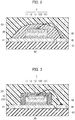
Fig. 1 illustrates the semiconductor device with the case of including the functional insulatingfilm 20 having a substantially uniform thickness and arranged on the top and the side surfaces of thesemiconductor chip 1, the functional insulatingfilm 20 is not limited to the configuration as illustrated inFig. 1 . For example, as illustrated inFig. 2 , the functional insulatingfilm 20 may be arranged into a liquid-drop state potted on the top surface of the substrate 40 (the same is also applied to the following modified examples). - A first modified example of the first embodiment is described below with reference to
Fig. 3. Fig. 3 illustrates the functional insulatingfilm 20 including a large amount ofmicrocrystal particles 210 composed of a conductor having the same band gap as or a narrower band gap than the semiconductor composing thesemiconductor chip 1. - The
microcrystal particles 210 include a large amount of crystal defects, which form various levels in the band gap. When the generated light enters themicrocrystal particles 210, a light having a longer wavelength is emitted, as in the case of the fluorescent substance described above. The functional insulatingfilm 20 including a large amount of themicrocrystal particles 210 thus has the same function as the fluorescent substance. - A constituent substance of the
microcrystal particles 210 can be the same as that of thesemiconductor chip 1. Alternatively, a material having a narrower band gap, such as microcrystals of Si inexpensive and easily available, may be used. A diameter of themicrocrystal particles 210 is preferably set to be sufficiently greater than the wavelength of the light emitted from thesemiconductor chip 1. A density of themicrocrystal particles 210 in the functional insulatingfilm 20 is designed so as not to allow the generated light to directly pass through the functional insulatingfilm 20 without hitting themicrocrystal particles 210. Themicrocrystal particles 210 are preferably formed in multiple layers in the functional insulatingfilm 20, as illustrated inFig. 3 . - As described above, the functional insulating
film 20 including themicrocrystal particles 210 can also achieve the same effects as described above with reference toFig. 1 . The configuration illustrated inFig. 3 does not necessarily include the fluorescent substance, and can make use of the microcrystal particles composed of the semiconductor of the same type as thesemiconductor chip 1 or the inexpensive microcrystal particles such as Si. The functional insulatingfilm 20 can include the same fluorescent substance as illustrated inFig. 1 with no limitation. - Resin typically has a greater coefficient of thermal expansion than a semiconductor. Using the
microcrystal particles 210 including the semiconductor in the sealingresin 30 can relax thermal stress caused between thesemiconductor chip 1 and the functional insulatingfilm 20 because of a change in temperature during use. The configuration illustrated inFig. 3 is also suitably used so as to avoid damage caused by the thermal stress. - A second modified example of the first embodiment is described below with reference to
Fig. 4. Fig. 4 is a cross-sectional view similar toFig. 1 . The functional insulatingfilm 20 illustrated inFig. 4 includesreflective particles 20 including a substance at least on the surface that reflects the ultraviolet light emitted from thesemiconductor chip 1. A density of the reflective particles 220 in the functional insulatingfilm 20 is also designed to be formed at least in multiple layers in the functional insulatingfilm 20 as illustrated inFig. 4 so as not to allow the light generated in thesemiconductor chip 1 to directly pass through the functional insulatingfilm 20 without hitting the reflective particles 220, as in the case illustrated inFig. 3 . - A constituent substance of the reflective particles 220 to be used is preferably zinc oxide or titanium oxide, for example. Since these substances have electrical conductivity, an insulating component of the functional insulating
film 20 should be interposed between the respective reflective particles 220. - A particle diameter and a deposited thickness of the reflective particles 220 are designed so as not to allow the generated light to reach the sealing
resin 30, as in the case of the first modified example. The particle diameter of the reflective particles 220 is preferably set to be greater than the wavelength of the generated light. - As described above, the functional insulating
film 20 including the reflective particles 220 that reflect the generated light can also achieve the effect of not allowing the generated light to reach the sealingresin 30. The functional insulatingfilm 20 including the reflective particles 220 also may further include the fluorescent substance. - A third modified example of the first embodiment is described below with reference to
Fig. 5. Fig. 5 is a partly-enlarged cross-sectional view of the functional insulatingfilm 20 adjacent to thesemiconductor chip 1. The functional insulatingfilm 20 illustrated inFig. 5 includesfluorescent microparticles 230, each including aparticulate base body 232 having a substantially spherical shape, and afluorescent layer 231 covering the surface of theparticulate base body 232. - The
particulate base body 232 is made of a material having a higher refractive index than the functional insulatingfilm 20. Choosing such a material for theparticulate base body 232 causes the generated light L entering the surface of the respectivefluorescent microparticles 230 at a shallow angle to advance in thefluorescent layer 231 including the fluorescent substance while being repeatedly refracted at the interfaces. The functional insulatingfilm 20 including thefluorescent microparticles 230 can efficiently convert the wavelength of the generated light L. - The
particulate base body 232 thus preferably has the substantially spherical shape, instead of a shape provided with an acute angle part. Theparticulate base body 232 may be made of any material that can suppress great deterioration when absorbing the generated light L. Theparticulate base body 232 may be made of the same material as themicrocrystal particles 210 and the reflective particles 220, or may be made of a different material. Thefluorescent layer 231 preferably has a thickness set to be greater than the wavelength of the generated light L. - In view of the coefficient of thermal expansion as in the case illustrated in
Fig. 3 , the material included in theparticulate base body 232 is preferably a substance having a small coefficient of thermal expansion, such as quartz glass having a low thermal-expansion coefficient, which is conventionally mixed in a sealing resin of a power semiconductor package, for example. The configuration as described above can provide the functional region while using a lower-priced material than themicrocrystal particles 210 as described with reference toFig. 3 . - A second embodiment of the present invention is described below with reference to
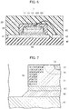
Fig. 6. Fig. 6 is a cross-sectional view of a semiconductor device similar to that illustrated inFig. 1 . The semiconductor device of this embodiment differs from that of the above embodiment in that the bondingmember 50 further extends between the side surface of thesemiconductor chip 1 and the functional insulatingfilm 20. - When the
bonding member 50 includes a ZnAl material, Zn in the solid ZnAl material when melted evaporates at a melding point or higher to turn into vapor, and adheres to the side surface of thesemiconductor chip 1. The molten ZnAl material comes up along the side surface of thesemiconductor chip 1 and is then solidified. A metal film of the ZnAl material included in thebonding member 50 is thus formed on the side surface of thesemiconductor chip 1 as illustrated inFig. 6 , so as to have a function of reflecting the generated light. - A third embodiment is described below with reference to
Fig. 7. Fig. 7 is an enlarged cross-sectional view illustrating only the part adjacent to the left side surface of thesemiconductor chip 1 illustrated inFig. 1 .Fig. 7 omits the illustration of the other elements including the sealingresin 30. The mark "×" indicates apolycrystal region 15 formed in an inactive region adjacent to the side wall of thesemiconductor chip 1. The term "inactive region" as used herein refers to a region not serving as a current path during the operation of thesemiconductor chip 1, and a region having no influence on a breakdown voltage upon reverse bias of thesemiconductor chip 1. In particular, the region is located at the circumference of the side wall of thesemiconductor chip 1. - The
polycrystal region 15 can be formed by use of a convergent pulse laser typically used for a laser stealth dicing method. The use of the convergent pulse laser can form the polycrystal region locally at an optional position in the semiconductor (refer to Non-Patent Literature 2). The object of the laser stealth dicing is to form a number of belt-like defect regions by this method so as to divide the semiconductor chip into parts with a relatively light external force. The present embodiment uses this method to locally form, in thesemiconductor chip 1, crystal defect regions having the same function as the fluorescent substance, as in the case of themicrocrystal particles 210 described with reference toFig. 3 . Reducing the laser output and forming multiple layers by local radiation at appropriate intervals can form a region that converts the ultraviolet light emitted from the inside of thesemiconductor chip 1 into a harmless light while avoiding unintended deterioration in mechanical strength. The provision of thepolycrystal region 15 in thesemiconductor chip 1 can eliminate the functional insulatingfilm 20 or can serve as a part of the function thereof, so as to ensure the effect of suppressing the deterioration of the sealing resin more easily. - The respective embodiments described above with reference to the drawings may be implemented independently, or may be combined and brought into operation simultaneously. It should be understood that the present invention includes any other embodiments other than the embodiments disclosed herein within the scope of the appended claims.
- While the embodiments have been illustrated above with the diode chip of the wide band-gap semiconductor as the
semiconductor chip 1, the present invention can also be effectively applied to a packaged structure of a MOSFET, a JFET, a bipolar transistor, an IGBT, or a thyristor that includes a p-n junction and allows a forward current to flow therethrough. - The semiconductor device according to the present invention can be used in electronics industries including manufacturing industries for manufacturing semiconductor devices having a resin-sealed packaged structure in which a semiconductor chip is sealed with resin.
-
- 1
- SEMICONDUCTOR CHIP
- 11
- n-TYPE SEMICONDUCTOR REGION
- 12
- p-TYPE SEMICONDUCTOR REGION
- 13
- p-n JUNCTION
- 14
- DEPLETION LAYER
- 15
- POLYCRYSTAL REGION
- 20
- FUNCTIONAL INSULATING FILM
- 30
- SEALING RESIN
- 40
- SUBSTRATE
- 41
- FIRST WIRING PATTERN
- 42
- SECOND WIRING PATTERN
- 50
- BONDING MEMBER
- 60
- METAL WIRE
- 101
- FIRST MAIN ELECTRODE
- 102
- SECOND MAIN ELECTRODE
- 210
- MICROCRYSTAL PARTICLE
- 220
- REFLECTIVE PARTICLE
- 230
- FLUORESCENT PARTICLE
- 231
- FLUORESCENT LAYER
- 232
- PARTICULATE BASE BODY
Claims (9)
- A semiconductor device comprising:a semiconductor chip provided inside with a p-n junction;an opaque sealing resin covering a surface of the semiconductor chip; anda functional region arranged between the semiconductor chip and the sealing resin and configured to prevent a light from reaching the sealing resin, the light being generated when a forward current flows through the p-n junction and having a particular wavelength causing deterioration of the sealing resin.
- The semiconductor device according to claim 1, wherein the functional region includes a functional insulating film having an insulating property and arranged between the semiconductor chip and the sealing resin.
- The semiconductor device according to claim 2, wherein the functional insulating film includes a fluorescent substance that converts the light having the particular wavelength into a light having a long wavelength.
- The semiconductor device according to claim 2, wherein the functional insulating film includes a fluorescent microparticle including the fluorescent substance that converts the light having the particular wavelength into the light having the long wavelength and covers a surface of a particulate base body having a higher refractive index than the functional insulating film.
- The semiconductor device according to claim 4, wherein the particulate base body has a smaller coefficient of thermal expansion than a base body of the functional insulating film.
- The semiconductor device according to claim 2, wherein the functional insulating film includes a microcrystal particle including a semiconductor having a band gap equal to or narrower than a semiconductor included in the semiconductor chip.
- The semiconductor device according to claim 2, wherein the functional insulating film includes a reflective particle including a substance that reflects the light having the particular wavelength at least on a surface of the reflective particle.
- The semiconductor device according to claim 1, further comprising:a substrate on which the semiconductor chip is mounted; anda bonding member including metal and electrically bonding a wiring pattern arranged on a top surface of the substrate with an electrode provided on a main surface of the semiconductor chip opposed to the top surface of the substrate,wherein the bonding member continuously extends along a side surface of the semiconductor chip.
- The semiconductor device according to claim 1, wherein the functional insulating film includes a plurality of crystal defect regions provided locally in an inactive region adjacent to a side surface of the semiconductor chip.
Applications Claiming Priority (1)
| Application Number | Priority Date | Filing Date | Title |
|---|---|---|---|
| PCT/JP2018/047844 WO2020136759A1 (en) | 2018-12-26 | 2018-12-26 | Semiconducor device |
Publications (3)
| Publication Number | Publication Date |
|---|---|
| EP3905317A1 true EP3905317A1 (en) | 2021-11-03 |
| EP3905317A4 EP3905317A4 (en) | 2022-01-12 |
| EP3905317B1 EP3905317B1 (en) | 2022-10-05 |
Family
ID=71126977
Family Applications (1)
| Application Number | Title | Priority Date | Filing Date |
|---|---|---|---|
| EP18944238.7A Active EP3905317B1 (en) | 2018-12-26 | 2018-12-26 | Semiconductor device |
Country Status (4)
| Country | Link |
|---|---|
| US (1) | US11462449B2 (en) |
| EP (1) | EP3905317B1 (en) |
| CN (1) | CN113228261B (en) |
| WO (1) | WO2020136759A1 (en) |
Families Citing this family (2)
| Publication number | Priority date | Publication date | Assignee | Title |
|---|---|---|---|---|
| JP2023013848A (en) * | 2021-07-16 | 2023-01-26 | 富士電機株式会社 | Semiconductor device |
| JP2024021137A (en) | 2022-08-03 | 2024-02-16 | 富士電機株式会社 | Silicon carbide semiconductor device and method for manufacturing a silicon carbide semiconductor device |
Family Cites Families (21)
| Publication number | Priority date | Publication date | Assignee | Title |
|---|---|---|---|---|
| JPS5681957A (en) | 1979-12-07 | 1981-07-04 | Hitachi Ltd | Semiconductor package using thermoplastic resin and manufacture thereof |
| JP3223835B2 (en) * | 1997-03-28 | 2001-10-29 | 三菱電機株式会社 | Power semiconductor device and method of manufacturing the same |
| JP3417297B2 (en) | 1998-06-12 | 2003-06-16 | 株式会社日立製作所 | Semiconductor device |
| JP2004047748A (en) * | 2002-07-12 | 2004-02-12 | Stanley Electric Co Ltd | Light emitting diode |
| JP2005317881A (en) | 2004-04-30 | 2005-11-10 | Citizen Electronics Co Ltd | Light emitting diode |
| JP2006310771A (en) * | 2005-03-30 | 2006-11-09 | Toshiba Discrete Technology Kk | Semiconductor light emitting device |
| CN101208811A (en) * | 2005-08-05 | 2008-06-25 | 松下电器产业株式会社 | semiconductor light emitting device |
| JP4915869B2 (en) | 2007-10-17 | 2012-04-11 | 日東電工株式会社 | Manufacturing method of optical semiconductor device |
| WO2009074919A1 (en) | 2007-12-11 | 2009-06-18 | Koninklijke Philips Electronics N.V. | Side emitting device with hybrid top reflector |
| JP2010219420A (en) | 2009-03-18 | 2010-09-30 | Fuji Electric Systems Co Ltd | Semiconductor device |
| JP2014120639A (en) | 2012-12-18 | 2014-06-30 | Rohm Co Ltd | Power module semiconductor device |
| JP5487290B2 (en) * | 2012-12-21 | 2014-05-07 | ルネサスエレクトロニクス株式会社 | Semiconductor device |
| WO2015157178A1 (en) | 2014-04-07 | 2015-10-15 | Crystal Is, Inc. | Ultraviolet light-emitting devices and methods |
| KR102222580B1 (en) * | 2014-07-30 | 2021-03-05 | 삼성전자주식회사 | Light emitting device package and display device including the same |
| WO2016162987A1 (en) | 2015-04-08 | 2016-10-13 | 株式会社日立製作所 | Semiconductor device and semiconductor module |
| JP6668757B2 (en) * | 2016-01-07 | 2020-03-18 | 日亜化学工業株式会社 | Light emitting device manufacturing method |
| KR102572819B1 (en) * | 2016-02-23 | 2023-08-30 | 쑤저우 레킨 세미컨덕터 컴퍼니 리미티드 | Fabricating method for light emitting module and display device |
| KR20170121777A (en) * | 2016-04-25 | 2017-11-03 | 삼성전자주식회사 | Semiconductor light emitting device |
| US11112685B2 (en) * | 2017-06-02 | 2021-09-07 | Nexdot | Color conversion layer and display apparatus having the same |
| JP6892997B2 (en) * | 2017-07-31 | 2021-06-23 | 国立研究開発法人産業技術総合研究所 | Semiconductor device |
| US10615319B2 (en) * | 2017-10-20 | 2020-04-07 | Nichia Corporation | Light emitting device |
-
2018
- 2018-12-26 WO PCT/JP2018/047844 patent/WO2020136759A1/en not_active Ceased
- 2018-12-26 CN CN201880100282.9A patent/CN113228261B/en active Active
- 2018-12-26 EP EP18944238.7A patent/EP3905317B1/en active Active
- 2018-12-26 US US17/417,854 patent/US11462449B2/en active Active
Also Published As
| Publication number | Publication date |
|---|---|
| CN113228261B (en) | 2022-12-23 |
| CN113228261A (en) | 2021-08-06 |
| US20220044980A1 (en) | 2022-02-10 |
| WO2020136759A1 (en) | 2020-07-02 |
| US11462449B2 (en) | 2022-10-04 |
| EP3905317A4 (en) | 2022-01-12 |
| EP3905317B1 (en) | 2022-10-05 |
Similar Documents
| Publication | Publication Date | Title |
|---|---|---|
| KR101007137B1 (en) | Light emitting device, light emitting device manufacturing method and light emitting device package | |
| CN102227807B (en) | Radiation-emitting semiconductor chip and its manufacture method | |
| US8384115B2 (en) | Bond pad design for enhancing light extraction from LED chips | |
| US8866169B2 (en) | LED package with increased feature sizes | |
| US7829911B2 (en) | Light emitting diode | |
| US7683396B2 (en) | High power light emitting device assembly utilizing ESD protective means sandwiched between dual sub-mounts | |
| US10224393B2 (en) | Method of producing semiconductor chips that efficiently dissipate heat | |
| KR101675652B1 (en) | Solid state transducer devices, including devices having integrated electrostatic discharge protection, and associated systems and methods | |
| KR20190031094A (en) | Light emitting device package and lighting apparatus | |
| CN101140975B (en) | Light emitting device | |
| US20110133224A1 (en) | Thermally optimised led chip-on-board module | |
| KR102329719B1 (en) | Light emitting device and light unit having thereof | |
| KR20110006650A (en) | Radiation emitting semiconductor chip | |
| CN107112404B (en) | Light emitting device | |
| TW201236207A (en) | Light-emitting diode device | |
| US10490701B2 (en) | Light emitting diode chip | |
| US11462449B2 (en) | Semiconductor device | |
| CN107195743A (en) | A kind of ultraviolet LED flip-chip | |
| Shei et al. | Improved reliability and ESD characteristics of flip-chip GaN-based LEDs with internal inverse-parallel protection diodes | |
| JP6892997B2 (en) | Semiconductor device | |
| Shih et al. | Role of transparent die attach adhesives for enhancing lumen output of midpower LED emitters with standard MESA structure | |
| US11448381B2 (en) | Light-emitting device with reflective ceramic substrate | |
| KR20200009764A (en) | Light emitting device package and light module | |
| JPH09298314A (en) | Light emitting device | |
| KR102412620B1 (en) | Light emitting device and lighting emitting apparatus having thereof |
Legal Events
| Date | Code | Title | Description |
|---|---|---|---|
| STAA | Information on the status of an ep patent application or granted ep patent |
Free format text: STATUS: THE INTERNATIONAL PUBLICATION HAS BEEN MADE |
|
| PUAI | Public reference made under article 153(3) epc to a published international application that has entered the european phase |
Free format text: ORIGINAL CODE: 0009012 |
|
| STAA | Information on the status of an ep patent application or granted ep patent |
Free format text: STATUS: REQUEST FOR EXAMINATION WAS MADE |
|
| 17P | Request for examination filed |
Effective date: 20210616 |
|
| AK | Designated contracting states |
Kind code of ref document: A1 Designated state(s): AL AT BE BG CH CY CZ DE DK EE ES FI FR GB GR HR HU IE IS IT LI LT LU LV MC MK MT NL NO PL PT RO RS SE SI SK SM TR |
|
| A4 | Supplementary search report drawn up and despatched |
Effective date: 20211209 |
|
| RIC1 | Information provided on ipc code assigned before grant |
Ipc: H01L 33/50 20100101ALN20211203BHEP Ipc: H01L 23/552 20060101ALI20211203BHEP Ipc: H01L 33/52 20100101ALI20211203BHEP Ipc: H01L 25/18 20060101ALI20211203BHEP Ipc: H01L 25/07 20060101ALI20211203BHEP Ipc: H01L 23/31 20060101ALI20211203BHEP Ipc: H01L 23/00 20060101ALI20211203BHEP Ipc: H01L 23/29 20060101AFI20211203BHEP |
|
| DAV | Request for validation of the european patent (deleted) | ||
| DAX | Request for extension of the european patent (deleted) | ||
| GRAP | Despatch of communication of intention to grant a patent |
Free format text: ORIGINAL CODE: EPIDOSNIGR1 |
|
| STAA | Information on the status of an ep patent application or granted ep patent |
Free format text: STATUS: GRANT OF PATENT IS INTENDED |
|
| RIC1 | Information provided on ipc code assigned before grant |
Ipc: H01L 33/50 20100101ALN20220630BHEP Ipc: H01L 23/552 20060101ALI20220630BHEP Ipc: H01L 33/52 20100101ALI20220630BHEP Ipc: H01L 25/18 20060101ALI20220630BHEP Ipc: H01L 25/07 20060101ALI20220630BHEP Ipc: H01L 23/31 20060101ALI20220630BHEP Ipc: H01L 23/00 20060101ALI20220630BHEP Ipc: H01L 23/29 20060101AFI20220630BHEP |
|
| INTG | Intention to grant announced |
Effective date: 20220715 |
|
| GRAS | Grant fee paid |
Free format text: ORIGINAL CODE: EPIDOSNIGR3 |
|
| GRAA | (expected) grant |
Free format text: ORIGINAL CODE: 0009210 |
|
| STAA | Information on the status of an ep patent application or granted ep patent |
Free format text: STATUS: THE PATENT HAS BEEN GRANTED |
|
| AK | Designated contracting states |
Kind code of ref document: B1 Designated state(s): AL AT BE BG CH CY CZ DE DK EE ES FI FR GB GR HR HU IE IS IT LI LT LU LV MC MK MT NL NO PL PT RO RS SE SI SK SM TR |
|
| REG | Reference to a national code |
Ref country code: GB Ref legal event code: FG4D |
|
| REG | Reference to a national code |
Ref country code: CH Ref legal event code: EP |
|
| REG | Reference to a national code |
Ref country code: AT Ref legal event code: REF Ref document number: 1523290 Country of ref document: AT Kind code of ref document: T Effective date: 20221015 |
|
| REG | Reference to a national code |
Ref country code: IE Ref legal event code: FG4D |
|
| REG | Reference to a national code |
Ref country code: DE Ref legal event code: R096 Ref document number: 602018041585 Country of ref document: DE |
|
| REG | Reference to a national code |
Ref country code: LT Ref legal event code: MG9D |
|
| REG | Reference to a national code |
Ref country code: NL Ref legal event code: MP Effective date: 20221005 |
|
| REG | Reference to a national code |
Ref country code: AT Ref legal event code: MK05 Ref document number: 1523290 Country of ref document: AT Kind code of ref document: T Effective date: 20221005 |
|
| PG25 | Lapsed in a contracting state [announced via postgrant information from national office to epo] |
Ref country code: NL Free format text: LAPSE BECAUSE OF FAILURE TO SUBMIT A TRANSLATION OF THE DESCRIPTION OR TO PAY THE FEE WITHIN THE PRESCRIBED TIME-LIMIT Effective date: 20221005 |
|
| PG25 | Lapsed in a contracting state [announced via postgrant information from national office to epo] |
Ref country code: SE Free format text: LAPSE BECAUSE OF FAILURE TO SUBMIT A TRANSLATION OF THE DESCRIPTION OR TO PAY THE FEE WITHIN THE PRESCRIBED TIME-LIMIT Effective date: 20221005 Ref country code: PT Free format text: LAPSE BECAUSE OF FAILURE TO SUBMIT A TRANSLATION OF THE DESCRIPTION OR TO PAY THE FEE WITHIN THE PRESCRIBED TIME-LIMIT Effective date: 20230206 Ref country code: NO Free format text: LAPSE BECAUSE OF FAILURE TO SUBMIT A TRANSLATION OF THE DESCRIPTION OR TO PAY THE FEE WITHIN THE PRESCRIBED TIME-LIMIT Effective date: 20230105 Ref country code: LT Free format text: LAPSE BECAUSE OF FAILURE TO SUBMIT A TRANSLATION OF THE DESCRIPTION OR TO PAY THE FEE WITHIN THE PRESCRIBED TIME-LIMIT Effective date: 20221005 Ref country code: FI Free format text: LAPSE BECAUSE OF FAILURE TO SUBMIT A TRANSLATION OF THE DESCRIPTION OR TO PAY THE FEE WITHIN THE PRESCRIBED TIME-LIMIT Effective date: 20221005 Ref country code: ES Free format text: LAPSE BECAUSE OF FAILURE TO SUBMIT A TRANSLATION OF THE DESCRIPTION OR TO PAY THE FEE WITHIN THE PRESCRIBED TIME-LIMIT Effective date: 20221005 Ref country code: AT Free format text: LAPSE BECAUSE OF FAILURE TO SUBMIT A TRANSLATION OF THE DESCRIPTION OR TO PAY THE FEE WITHIN THE PRESCRIBED TIME-LIMIT Effective date: 20221005 |
|
| PG25 | Lapsed in a contracting state [announced via postgrant information from national office to epo] |
Ref country code: RS Free format text: LAPSE BECAUSE OF FAILURE TO SUBMIT A TRANSLATION OF THE DESCRIPTION OR TO PAY THE FEE WITHIN THE PRESCRIBED TIME-LIMIT Effective date: 20221005 Ref country code: PL Free format text: LAPSE BECAUSE OF FAILURE TO SUBMIT A TRANSLATION OF THE DESCRIPTION OR TO PAY THE FEE WITHIN THE PRESCRIBED TIME-LIMIT Effective date: 20221005 Ref country code: LV Free format text: LAPSE BECAUSE OF FAILURE TO SUBMIT A TRANSLATION OF THE DESCRIPTION OR TO PAY THE FEE WITHIN THE PRESCRIBED TIME-LIMIT Effective date: 20221005 Ref country code: IS Free format text: LAPSE BECAUSE OF FAILURE TO SUBMIT A TRANSLATION OF THE DESCRIPTION OR TO PAY THE FEE WITHIN THE PRESCRIBED TIME-LIMIT Effective date: 20230205 Ref country code: HR Free format text: LAPSE BECAUSE OF FAILURE TO SUBMIT A TRANSLATION OF THE DESCRIPTION OR TO PAY THE FEE WITHIN THE PRESCRIBED TIME-LIMIT Effective date: 20221005 Ref country code: GR Free format text: LAPSE BECAUSE OF FAILURE TO SUBMIT A TRANSLATION OF THE DESCRIPTION OR TO PAY THE FEE WITHIN THE PRESCRIBED TIME-LIMIT Effective date: 20230106 |
|
| REG | Reference to a national code |
Ref country code: DE Ref legal event code: R097 Ref document number: 602018041585 Country of ref document: DE |
|
| PG25 | Lapsed in a contracting state [announced via postgrant information from national office to epo] |
Ref country code: SM Free format text: LAPSE BECAUSE OF FAILURE TO SUBMIT A TRANSLATION OF THE DESCRIPTION OR TO PAY THE FEE WITHIN THE PRESCRIBED TIME-LIMIT Effective date: 20221005 Ref country code: RO Free format text: LAPSE BECAUSE OF FAILURE TO SUBMIT A TRANSLATION OF THE DESCRIPTION OR TO PAY THE FEE WITHIN THE PRESCRIBED TIME-LIMIT Effective date: 20221005 Ref country code: EE Free format text: LAPSE BECAUSE OF FAILURE TO SUBMIT A TRANSLATION OF THE DESCRIPTION OR TO PAY THE FEE WITHIN THE PRESCRIBED TIME-LIMIT Effective date: 20221005 Ref country code: DK Free format text: LAPSE BECAUSE OF FAILURE TO SUBMIT A TRANSLATION OF THE DESCRIPTION OR TO PAY THE FEE WITHIN THE PRESCRIBED TIME-LIMIT Effective date: 20221005 Ref country code: CZ Free format text: LAPSE BECAUSE OF FAILURE TO SUBMIT A TRANSLATION OF THE DESCRIPTION OR TO PAY THE FEE WITHIN THE PRESCRIBED TIME-LIMIT Effective date: 20221005 |
|
| REG | Reference to a national code |
Ref country code: CH Ref legal event code: PL |
|
| PLBE | No opposition filed within time limit |
Free format text: ORIGINAL CODE: 0009261 |
|
| STAA | Information on the status of an ep patent application or granted ep patent |
Free format text: STATUS: NO OPPOSITION FILED WITHIN TIME LIMIT |
|
| REG | Reference to a national code |
Ref country code: BE Ref legal event code: MM Effective date: 20221231 |
|
| PG25 | Lapsed in a contracting state [announced via postgrant information from national office to epo] |
Ref country code: SK Free format text: LAPSE BECAUSE OF FAILURE TO SUBMIT A TRANSLATION OF THE DESCRIPTION OR TO PAY THE FEE WITHIN THE PRESCRIBED TIME-LIMIT Effective date: 20221005 Ref country code: LU Free format text: LAPSE BECAUSE OF NON-PAYMENT OF DUE FEES Effective date: 20221226 Ref country code: AL Free format text: LAPSE BECAUSE OF FAILURE TO SUBMIT A TRANSLATION OF THE DESCRIPTION OR TO PAY THE FEE WITHIN THE PRESCRIBED TIME-LIMIT Effective date: 20221005 |
|
| 26N | No opposition filed |
Effective date: 20230706 |
|
| PG25 | Lapsed in a contracting state [announced via postgrant information from national office to epo] |
Ref country code: LI Free format text: LAPSE BECAUSE OF NON-PAYMENT OF DUE FEES Effective date: 20221231 Ref country code: IE Free format text: LAPSE BECAUSE OF NON-PAYMENT OF DUE FEES Effective date: 20221226 Ref country code: CH Free format text: LAPSE BECAUSE OF NON-PAYMENT OF DUE FEES Effective date: 20221231 |
|
| PG25 | Lapsed in a contracting state [announced via postgrant information from national office to epo] |
Ref country code: SI Free format text: LAPSE BECAUSE OF FAILURE TO SUBMIT A TRANSLATION OF THE DESCRIPTION OR TO PAY THE FEE WITHIN THE PRESCRIBED TIME-LIMIT Effective date: 20221005 Ref country code: BE Free format text: LAPSE BECAUSE OF NON-PAYMENT OF DUE FEES Effective date: 20221231 |
|
| PG25 | Lapsed in a contracting state [announced via postgrant information from national office to epo] |
Ref country code: CY Free format text: LAPSE BECAUSE OF FAILURE TO SUBMIT A TRANSLATION OF THE DESCRIPTION OR TO PAY THE FEE WITHIN THE PRESCRIBED TIME-LIMIT Effective date: 20221005 |
|
| PG25 | Lapsed in a contracting state [announced via postgrant information from national office to epo] |
Ref country code: MK Free format text: LAPSE BECAUSE OF FAILURE TO SUBMIT A TRANSLATION OF THE DESCRIPTION OR TO PAY THE FEE WITHIN THE PRESCRIBED TIME-LIMIT Effective date: 20221005 Ref country code: IT Free format text: LAPSE BECAUSE OF FAILURE TO SUBMIT A TRANSLATION OF THE DESCRIPTION OR TO PAY THE FEE WITHIN THE PRESCRIBED TIME-LIMIT Effective date: 20221005 Ref country code: HU Free format text: LAPSE BECAUSE OF FAILURE TO SUBMIT A TRANSLATION OF THE DESCRIPTION OR TO PAY THE FEE WITHIN THE PRESCRIBED TIME-LIMIT; INVALID AB INITIO Effective date: 20181226 |
|
| PG25 | Lapsed in a contracting state [announced via postgrant information from national office to epo] |
Ref country code: MC Free format text: LAPSE BECAUSE OF FAILURE TO SUBMIT A TRANSLATION OF THE DESCRIPTION OR TO PAY THE FEE WITHIN THE PRESCRIBED TIME-LIMIT Effective date: 20221005 |
|
| PG25 | Lapsed in a contracting state [announced via postgrant information from national office to epo] |
Ref country code: MC Free format text: LAPSE BECAUSE OF FAILURE TO SUBMIT A TRANSLATION OF THE DESCRIPTION OR TO PAY THE FEE WITHIN THE PRESCRIBED TIME-LIMIT Effective date: 20221005 |
|
| PG25 | Lapsed in a contracting state [announced via postgrant information from national office to epo] |
Ref country code: BG Free format text: LAPSE BECAUSE OF FAILURE TO SUBMIT A TRANSLATION OF THE DESCRIPTION OR TO PAY THE FEE WITHIN THE PRESCRIBED TIME-LIMIT Effective date: 20221005 |
|
| PG25 | Lapsed in a contracting state [announced via postgrant information from national office to epo] |
Ref country code: MT Free format text: LAPSE BECAUSE OF FAILURE TO SUBMIT A TRANSLATION OF THE DESCRIPTION OR TO PAY THE FEE WITHIN THE PRESCRIBED TIME-LIMIT Effective date: 20221005 |
|
| REG | Reference to a national code |
Ref country code: DE Ref legal event code: R079 Ref document number: 602018041585 Country of ref document: DE Free format text: PREVIOUS MAIN CLASS: H01L0023290000 Ipc: H10W0074400000 |
|
| PG25 | Lapsed in a contracting state [announced via postgrant information from national office to epo] |
Ref country code: TR Free format text: LAPSE BECAUSE OF FAILURE TO SUBMIT A TRANSLATION OF THE DESCRIPTION OR TO PAY THE FEE WITHIN THE PRESCRIBED TIME-LIMIT Effective date: 20221005 |
|
| PGFP | Annual fee paid to national office [announced via postgrant information from national office to epo] |
Ref country code: DE Payment date: 20251126 Year of fee payment: 8 |
|
| PGFP | Annual fee paid to national office [announced via postgrant information from national office to epo] |
Ref country code: GB Payment date: 20251119 Year of fee payment: 8 |
|
| PGFP | Annual fee paid to national office [announced via postgrant information from national office to epo] |
Ref country code: FR Payment date: 20251120 Year of fee payment: 8 |