EP3904920A1 - Display device and method of manufacturing the same - Google Patents
Display device and method of manufacturing the same Download PDFInfo
- Publication number
- EP3904920A1 EP3904920A1 EP21162247.7A EP21162247A EP3904920A1 EP 3904920 A1 EP3904920 A1 EP 3904920A1 EP 21162247 A EP21162247 A EP 21162247A EP 3904920 A1 EP3904920 A1 EP 3904920A1
- Authority
- EP
- European Patent Office
- Prior art keywords
- region
- reflection
- layer
- display device
- reflection layer
- Prior art date
- Legal status (The legal status is an assumption and is not a legal conclusion. Google has not performed a legal analysis and makes no representation as to the accuracy of the status listed.)
- Granted
Links
Images





Classifications
-
- G—PHYSICS
- G02—OPTICS
- G02B—OPTICAL ELEMENTS, SYSTEMS OR APPARATUS
- G02B1/00—Optical elements characterised by the material of which they are made; Optical coatings for optical elements
- G02B1/10—Optical coatings produced by application to, or surface treatment of, optical elements
- G02B1/11—Anti-reflection coatings
- G02B1/113—Anti-reflection coatings using inorganic layer materials only
- G02B1/115—Multilayers
-
- H—ELECTRICITY
- H10—SEMICONDUCTOR DEVICES; ELECTRIC SOLID-STATE DEVICES NOT OTHERWISE PROVIDED FOR
- H10K—ORGANIC ELECTRIC SOLID-STATE DEVICES
- H10K50/00—Organic light-emitting devices
- H10K50/80—Constructional details
- H10K50/86—Arrangements for improving contrast, e.g. preventing reflection of ambient light
-
- H—ELECTRICITY
- H10—SEMICONDUCTOR DEVICES; ELECTRIC SOLID-STATE DEVICES NOT OTHERWISE PROVIDED FOR
- H10D—INORGANIC ELECTRIC SEMICONDUCTOR DEVICES
- H10D86/00—Integrated devices formed in or on insulating or conducting substrates, e.g. formed in silicon-on-insulator [SOI] substrates or on stainless steel or glass substrates
- H10D86/01—Manufacture or treatment
- H10D86/021—Manufacture or treatment of multiple TFTs
- H10D86/0212—Manufacture or treatment of multiple TFTs comprising manufacture, treatment or coating of substrates
-
- H—ELECTRICITY
- H10—SEMICONDUCTOR DEVICES; ELECTRIC SOLID-STATE DEVICES NOT OTHERWISE PROVIDED FOR
- H10D—INORGANIC ELECTRIC SEMICONDUCTOR DEVICES
- H10D86/00—Integrated devices formed in or on insulating or conducting substrates, e.g. formed in silicon-on-insulator [SOI] substrates or on stainless steel or glass substrates
- H10D86/40—Integrated devices formed in or on insulating or conducting substrates, e.g. formed in silicon-on-insulator [SOI] substrates or on stainless steel or glass substrates characterised by multiple TFTs
- H10D86/411—Integrated devices formed in or on insulating or conducting substrates, e.g. formed in silicon-on-insulator [SOI] substrates or on stainless steel or glass substrates characterised by multiple TFTs characterised by materials, geometry or structure of the substrates
-
- H—ELECTRICITY
- H10—SEMICONDUCTOR DEVICES; ELECTRIC SOLID-STATE DEVICES NOT OTHERWISE PROVIDED FOR
- H10K—ORGANIC ELECTRIC SOLID-STATE DEVICES
- H10K50/00—Organic light-emitting devices
- H10K50/80—Constructional details
- H10K50/84—Passivation; Containers; Encapsulations
- H10K50/844—Encapsulations
- H10K50/8445—Encapsulations multilayered coatings having a repetitive structure, e.g. having multiple organic-inorganic bilayers
-
- H—ELECTRICITY
- H10—SEMICONDUCTOR DEVICES; ELECTRIC SOLID-STATE DEVICES NOT OTHERWISE PROVIDED FOR
- H10K—ORGANIC ELECTRIC SOLID-STATE DEVICES
- H10K50/00—Organic light-emitting devices
- H10K50/80—Constructional details
- H10K50/86—Arrangements for improving contrast, e.g. preventing reflection of ambient light
- H10K50/865—Arrangements for improving contrast, e.g. preventing reflection of ambient light comprising light absorbing layers, e.g. light-blocking layers
-
- H—ELECTRICITY
- H10—SEMICONDUCTOR DEVICES; ELECTRIC SOLID-STATE DEVICES NOT OTHERWISE PROVIDED FOR
- H10K—ORGANIC ELECTRIC SOLID-STATE DEVICES
- H10K59/00—Integrated devices, or assemblies of multiple devices, comprising at least one organic light-emitting element covered by group H10K50/00
-
- H—ELECTRICITY
- H10—SEMICONDUCTOR DEVICES; ELECTRIC SOLID-STATE DEVICES NOT OTHERWISE PROVIDED FOR
- H10K—ORGANIC ELECTRIC SOLID-STATE DEVICES
- H10K59/00—Integrated devices, or assemblies of multiple devices, comprising at least one organic light-emitting element covered by group H10K50/00
- H10K59/10—OLED displays
- H10K59/12—Active-matrix OLED [AMOLED] displays
- H10K59/121—Active-matrix OLED [AMOLED] displays characterised by the geometry or disposition of pixel elements
-
- H—ELECTRICITY
- H10—SEMICONDUCTOR DEVICES; ELECTRIC SOLID-STATE DEVICES NOT OTHERWISE PROVIDED FOR
- H10K—ORGANIC ELECTRIC SOLID-STATE DEVICES
- H10K59/00—Integrated devices, or assemblies of multiple devices, comprising at least one organic light-emitting element covered by group H10K50/00
- H10K59/80—Constructional details
- H10K59/8791—Arrangements for improving contrast, e.g. preventing reflection of ambient light
-
- H—ELECTRICITY
- H10—SEMICONDUCTOR DEVICES; ELECTRIC SOLID-STATE DEVICES NOT OTHERWISE PROVIDED FOR
- H10K—ORGANIC ELECTRIC SOLID-STATE DEVICES
- H10K71/00—Manufacture or treatment specially adapted for the organic devices covered by this subclass
-
- H—ELECTRICITY
- H10—SEMICONDUCTOR DEVICES; ELECTRIC SOLID-STATE DEVICES NOT OTHERWISE PROVIDED FOR
- H10K—ORGANIC ELECTRIC SOLID-STATE DEVICES
- H10K59/00—Integrated devices, or assemblies of multiple devices, comprising at least one organic light-emitting element covered by group H10K50/00
- H10K59/10—OLED displays
- H10K59/12—Active-matrix OLED [AMOLED] displays
- H10K59/122—Pixel-defining structures or layers, e.g. banks
-
- H—ELECTRICITY
- H10—SEMICONDUCTOR DEVICES; ELECTRIC SOLID-STATE DEVICES NOT OTHERWISE PROVIDED FOR
- H10K—ORGANIC ELECTRIC SOLID-STATE DEVICES
- H10K59/00—Integrated devices, or assemblies of multiple devices, comprising at least one organic light-emitting element covered by group H10K50/00
- H10K59/10—OLED displays
- H10K59/12—Active-matrix OLED [AMOLED] displays
- H10K59/124—Insulating layers formed between TFT elements and OLED elements
-
- H—ELECTRICITY
- H10—SEMICONDUCTOR DEVICES; ELECTRIC SOLID-STATE DEVICES NOT OTHERWISE PROVIDED FOR
- H10K—ORGANIC ELECTRIC SOLID-STATE DEVICES
- H10K59/00—Integrated devices, or assemblies of multiple devices, comprising at least one organic light-emitting element covered by group H10K50/00
- H10K59/30—Devices specially adapted for multicolour light emission
- H10K59/35—Devices specially adapted for multicolour light emission comprising red-green-blue [RGB] subpixels
-
- H—ELECTRICITY
- H10—SEMICONDUCTOR DEVICES; ELECTRIC SOLID-STATE DEVICES NOT OTHERWISE PROVIDED FOR
- H10K—ORGANIC ELECTRIC SOLID-STATE DEVICES
- H10K59/00—Integrated devices, or assemblies of multiple devices, comprising at least one organic light-emitting element covered by group H10K50/00
- H10K59/80—Constructional details
- H10K59/87—Passivation; Containers; Encapsulations
- H10K59/873—Encapsulations
Definitions
- a display device may provide visual information to a user by displaying an image.
- the display device may include a display panel for converting an electrical signal into an image.
- the display panel may include a light transmission region through which external light incident to the display device transmits. Through the light transmission region, functional modules such as a camera module and a sensor module disposed on a rear side of the display panel may detect or recognize an object and a user positioned in front of the display panel.
- Embodiments provide a display device in which external light reflection is reduced.
- a display device may include a display panel having a first region and a second region having a transmittance lower than a transmittance of the first region, the display panel including a substrate and a pixel layer disposed on the substrate, and an anti-reflection layer disposed on one side of the substrate in an area corresponding to the first region.
- the anti-reflection layer may include a first anti-reflection pattern including first metal and a second anti-reflection pattern disposed on the first anti-reflection pattern and including molybdenum oxide (MoO x ) and oxide of second metal other than molybdenum.
- the anti-reflection layer may overlap the first region and does not overlap the second region.
- the first metal may include at least one of molybdenum (Mo), aluminum (Al), and titanium (Ti).
- the second metal may include at least one of tantalum (Ta), tungsten (W), niobium (Nb), and copper (Cu).
- a ratio of the second metal to molybdenum in the second anti-reflection pattern may be greater than 0 at.% and less than about 20 at.%.
- the molybdenum oxide included in the second anti-reflection pattern and the oxide of the second metal may have a crystalline structure.
- the anti-reflection layer may be disposed on a bottom surface of the substrate, and the first anti-reflection pattern may be disposed between the substrate and the second anti-reflection pattern.
- the anti-reflection layer may be disposed on a top surface of the substrate, and the second anti-reflection pattern may be disposed between the substrate and the first anti-reflection pattern.
- the second anti-reflection pattern may have a thickness greater than about 10 nm [100 ⁇ ] and smaller than about 100 nm [1000 ⁇ ].
- a side-wall of the anti-reflection layer may be inclined with respect to the substrate.
- the second anti-reflection pattern may have a reflectivity less than a reflectivity of the first anti-reflection pattern.
- the first region may include a first pixel region, a transmission region, and a first peripheral region surrounding the first pixel region and the transmission region.
- the anti-reflection layer may overlap the first pixel region and the first peripheral region and may not overlap the transmission region.
- the second region may include a second pixel region and a second peripheral region surrounding the second pixel region.
- the second region may surround at least a part of the first region.
- the display device may further include a functional module disposed under the display panel in an area corresponding to the first region.
- the functional module may include at least one of a camera module, a face recognition sensor module, a pupil recognition sensor module, an acceleration sensor module, a proximity sensor module, an infrared sensor module, and an illuminance sensor module.
- a method of manufacturing a display device may include forming a first anti-reflection layer including first metal on a substrate having a first region and a second region that has a transmittance lower than the first region, forming a second anti-reflection layer including molybdenum oxide (MoO x ) and oxide of second metal other than molybdenum, and forming an anti-reflection layer in an area corresponding to the first region of the display panel by etching the first anti-reflection layer and the second anti-reflection layer through a single etching process using one mask.
- MoO x molybdenum oxide
- the first anti-reflection layer and the second anti-reflection layer may be etched through a dry etching.
- the method may further include cleaning the substrate including the first anti-reflection layer and the second anti-reflection layer by deionized water, before etching the first anti-reflection layer and the second anti-reflection layer.
- the display device may include the anti-reflection layer disposed on one side of the substrate corresponding to the first region and including the first anti-reflection pattern including first metal and the second anti-reflection pattern including molybdenum oxide (MoO x ) and oxide of second metal other than molybdenum so that the reflection of the external light passing through the first region may be reduced or substantially prevented. Accordingly, ghost image due to interference and reflection of the external light in the first region may not be recognized.
- MoO x molybdenum oxide
- FIGS. 1 to 6 a display device according to one embodiment will be described with reference to FIGS. 1 to 6 .
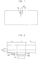
- FIG. 1 is a plan view showing a part of the display device according to one embodiment of the present inventive concept.
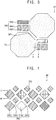
- FIG. 2 is a sectional view showing one example taken along line I-I' of FIG. 1 .
- the display device may include a display panel 100, an anti-reflection layer 200, and a functional module 300.
- the display panel 100 may have a first region A1 and a second region A2.
- Each of the first region A1 and the second region A2 may be a display region for displaying an image.
- the first region A1 may include a transmission region for allowing external light to be transmitted therethrough.
- the transmittance of the first region A1 may be higher than the transmittance of the second region A2.
- the transmittance of the second region A2 may be lower than the transmittance of the first region A1.
- the first region A1 may allow the external light to be transmitted therethrough while displaying the image.
- the first region A1 and the second region A2 may be disposed adjacent to each other.
- the second region A2 may surround at least a part of the first region A1.
- the first region A1 may be spaced apart from an edge of the display panel 100 and disposed in the display panel 100 when viewed from the top, and the second region A2 may completely surround the first region A1.
- the first region A1 may have a circular shape when viewed from the top.
- the present inventive concept is not limited thereto.
- the first region A1 may have various polygonal shapes when viewed from the top.
- the display panel 100 may include a substrate 110 and a pixel layer DP.
- the pixel layer DP may be disposed on the substrate 110.
- the pixel layer DP may include pixels for displaying the image.
- the anti-reflection layer 200 may be disposed on the bottom surface 110L of the substrate 110 corresponding to the first region A1.
- the anti-reflection layer 200 may reduce or substantially prevent the external light incident to the first region A1 from being reflected from the bottom surface 110L or interfaces between adjacent layers that form the pixel layer in the first region A1.
- the anti-reflection layer 200 may overlap the first region A1 and may not overlap the second region A2. In other words, the anti-reflection layer 200 may be disposed only on the bottom surface 110L of the substrate 110 corresponding to the first region A1, and may not be disposed on the bottom surface 110L of the substrate 110 corresponding to the second region A2. The first region A1 may completely overlap with the anti-reflection layer 200 in a plan view.
- the anti-reflection layer 200 may include a first anti-reflection pattern 210 and a second anti-reflection pattern 220.
- the second anti-reflection pattern 220 may be disposed on the first anti-reflection pattern 210.
- the first anti-reflection pattern 210 may be disposed between the substrate 110 and the second anti-reflection pattern 220.
- the first anti-reflection pattern 210 may be disposed on a bottom surface 110L of the substrate 110
- the second anti-reflection pattern 220 may be disposed on a bottom surface 210L of the first anti-reflection pattern 210.
- the first anti-reflection pattern 210 may include first metal.
- the first metal may include at least one of molybdenum (Mo), aluminum (Al), and titanium (Ti).
- Mo molybdenum
- Al aluminum
- Ti titanium
- the first anti-reflection pattern 210 may reduce reflection of the external light that is incident through the first region A1.
- the second anti-reflection pattern 220 may include molybdenum oxide (MoO x ) and oxide of second metal other than molybdenum (Mo).
- the second metal may include at least one of tantalum (Ta), tungsten (W), niobium (Nb), and copper (Cu).
- the second anti-reflection pattern 220 may include molybdenum oxide (MoO x ) and tantalum oxide (TaO y ).
- the second anti-reflection pattern 220 may absorb the external light incident through the first region A1, so that the reflection of the external light may be reduced or substantially prevented.
- Molybdenum oxide may absorb the external light in the second anti-reflection pattern 220, thereby functioning to reduce the reflectivity of the second anti-reflection pattern 220.
- the second anti-reflection pattern 220 may function as a black matrix.
- the oxide of the second metal in the second anti-reflection pattern 220 may serve to prevent a damage to the second anti-reflection pattern 220.
- a process of washing the second anti-reflection pattern 220 by using deionized water (DI water) may be performed.
- DI water deionized water
- the molybdenum oxide included in the second anti-reflection pattern 220 may be dissolved by the deionized water during the washing process, so that the second anti-reflection pattern 220 may be damaged.
- the second anti-reflection pattern 220 when the second anti-reflection pattern 220 includes the oxide of the second metal, the second anti-reflection pattern 220 may not be dissolved by the deionized water, and the damage to the second anti-reflection pattern 220 during the washing process may be prevented.
- the ratio of the second metal to molybdenum (Mo) in the second anti-reflection pattern 220 may be greater than 0 at.% and less than about 20 at.%.
- the ratio of the second metal to molybdenum (Mo) in the second anti-reflection pattern 220 is 0 at.%, the second anti-reflection pattern 220 may be damaged in the process of the washing the second anti-reflection pattern 220 as described above.
- the ratio of the second metal to molybdenum (Mo) in the second anti-reflection pattern 220 is greater than about 20 at.%, the reflectivity of the second anti-reflection pattern 220 may exceed a predetermined reflectivity (for example, about 20%).
- the ratio of the second metal to molybdenum (Mo) in the second anti-reflection pattern 220 is greater than about 20 at.%, the etching properties of the second anti-reflection pattern 220 may be deteriorated.
- the reflectivity of the second anti-reflection pattern 220 may be smaller than the reflectivity of the first anti-reflection pattern 210.
- the anti-reflection layer 200 may not sufficiently reduce the reflection of the external light incident through the first region A1.
- the second anti-reflection layer 220 having the reflectivity smaller than that of the first anti-reflection pattern 210 is disposed on the first anti-reflection pattern 210 , the reflection of the external light incident through the first region A1 may be sufficiently reduced or substantially prevented.
- the functional module 300 may be disposed under the display panel 100 in an area corresponding to the first region A1. In one embodiment, the functional module 300 may be disposed on the bottom surface 200L of the anti-reflection layer 200 in an area corresponding to the first region A1. The functional module 300 may receive the external light passing through the first region A1.
- the functional module 300 may include a camera module configured to photograph (or recognize) an image of the object positioned in front of the display device, a face recognition sensor module configured to sense a face of a user, a pupil recognition sensor module configured to sense a pupil of the user, an acceleration sensor module and a geomagnetic sensor module configured to determine a movement of the display device, a proximity sensor module and an infrared sensor module configured to detect a proximity to a front of the display device, and an illuminance sensor module configured to measure an external brightness.
- a camera module configured to photograph (or recognize) an image of the object positioned in front of the display device
- a face recognition sensor module configured to sense a face of a user
- a pupil recognition sensor module configured to sense a pupil of the user
- an acceleration sensor module and a geomagnetic sensor module configured to determine a movement of the display device
- a proximity sensor module and an infrared sensor module configured to detect a proximity to a front of the display device
- the display device When the external light passes through the first region A1 having a relatively small area a light interference may occur, and when the interfered external light is reflected by the display panel 100 and/or the functional module 300, the user may visually recognize a ghost image or the like displayed in the first region A1.
- the display device includes the anti-reflection layer 200 disposed on the bottom surface 110L of the substrate 110 in the area corresponding to the first region A1, and thus the anti-reflection layer 200 may absorb the external light even when the light interference occurs from the external light passing through the first region A1, so that the reflection of the external light may be reduced or substantially prevented. Accordingly, the user may be prevented from visually recognizing the ghost image or the like.
- FIG. 3 is a plan view showing the first region A1 of the display device of FIG. 1 .
- FIG. 4 is a plan view showing the second region A2 of the display device of FIG. 1 .
- the first region A1 may include a first pixel region PA1, a transmission region TA, and a first peripheral region SA1
- the second region A2 may include a second pixel region PA2 and a second peripheral region SA2.
- Each of the first pixel region PA1 and the second pixel region PA2 may be a region in which pixels are disposed to emit light generated from each of the pixels thereby displaying an image.
- the first pixel region PA1 may include a plurality of first sub-pixel regions SRA1, SGA1, and SBA1 emitting light having mutually different colors
- the second pixel region PA2 may include a plurality of second sub-pixel regions SRA2, SGA2, and SBA2 emitting light having mutually different colors.
- the sub-pixel regions SRA1, SGA1, and SBA1 may include a first red pixel region SRA1 emitting red light, a first green pixel region SGA1 emitting green light, and a first blue pixel region SBA1 emitting blue light
- the second sub-pixel regions SRA2, SGA2, and SBA2 may include a second red pixel region SRA2 emitting red light, a second green pixel region SGA2 emitting green light, and a second blue pixel region SBA2 emitting blue light.
- the transmission region TA may be a region in which no sub-pixels is disposed and that transmits the external light incident to the display panel 100.
- the functional module 300 disposed under the display panel 100 in the area corresponding to the first region A1 may easily detect or recognize the object or the user positioned in front of the display device through the transmission region TA.
- the first peripheral region SA1 may surround the first pixel region PA1 and the transmission region TA.
- the second peripheral region SA2 may surround the second pixel area PA2.
- Each of the first peripheral region SA1 and the second peripheral region SA2 may be a region in which light is not emitted and external light is not transmitted.
- the number of first sub-pixel regions SRA1, SGA1, and SBA1 per unit area may be smaller than the number of second sub-pixel regions SRA2, SGA2, and SBA2 per unit area in the second region A2.
- a resolution of the first region A1 may be less than a resolution of the second region A2.
- an arrangement structure of the first sub-pixel regions SRA1, SGA1, and SBA1 the first region A1 may be different from an arrangement structure of the second sub-pixel regions SRA2, SGA2, and SBA2 the second region A2.
- the first sub-pixel regions SRA1, SGA1, and SBA1 may be arranged in a stripe manner
- the second sub-pixel regions SRA2, SGA2, and SBA2 may be arranged in a PenTile manner.
- the first pixel region PA1 may include one first red pixel region SRA1, one first green pixel region SGA1, and one first blue pixel region SBA1
- the second pixel region PA2 may include one second red pixel region SRA2, two second green pixel regions SGA2, and one second blue pixel region SBA2.
- FIG. 5 is a sectional view taken along line II-II' of FIG. 3 .
- FIG. 6 is a sectional view taken along line III-III' of FIG. 4 .
- the display panel 100 may include a substrate 110 and a pixel layer DP.
- the pixel layer DP may include an active layer 120, a plurality of conductive layers 130, 141, and 142, a plurality of inorganic insulating layers 111 and 112, an organic insulating layer 113, a first electrode 150, a pixel defining layer 114, a light emitting layer 160, a second electrode 170, and an encapsulation layer 180.
- the substrate 110 may be a transparent insulating substrate.
- the substrate 110 may be formed of glass, quartz, plastic, or the like.
- the active layer 120 may be disposed on the substrate 110.
- the conductive layers 130, 141, and 142 may be disposed on the substrate 110 on different layers.
- the conductive layers 130, 141, and 142 may include a gate electrode 130, a source electrode 141, and a drain electrode 142.
- the active layer 120 and the conductive layers 130, 141 and 142 may be disposed in the first pixel region PA1, the first peripheral region SA1, the second pixel region PA2, and the second peripheral region SA2.
- the inorganic insulating layers 111 and 112 which are disposed on different layers to insulate the active layer 120 and the conductive layers 130, 141 and 142 from each other, may be disposed on the substrate 110.
- the inorganic insulating layers 111 and 112 may include a gate insulating layer 111 and an interlayer insulating layer 112.
- the active layer 120 may be disposed on the substrate 110.
- the active layer 120 may be formed of amorphous silicon, polycrystalline silicon, oxide semiconductor, or the like.
- the active layer 120 may include a source region, a drain region, and a channel region disposed between the source region and the drain region. P-type or N-type impurities may be doped in the source region and the drain region, and impurities may not be doped in the channel region.
- the gate insulating layer 111 may be disposed on the active layer 120.
- the gate insulating layer 111 may be formed on the substrate 110 while covering the active layer 120.
- the gate insulating layer 111 may insulate the gate electrode 130 from the active layer 120.
- the gate insulating layer 111 may be formed of an inorganic insulating material such as silicon nitride, and silicon oxide, silicon oxynitride.
- the gate electrode 130 may be disposed on the gate insulating layer 111.
- the gate electrode 130 may overlap the channel region of the active layer 120.
- the gate electrode 130 may be formed of a conductive material such as metal or a metal alloy.
- the gate electrode 130 may be formed of molybdenum (Mo), copper (Cu), and the like.
- An interlayer insulating layer 112 may be disposed on the gate electrode 130.
- the interlayer insulating layer 112 may be formed on the gate insulating layer 111 while covering the gate electrode 130.
- the interlayer insulating layer 112 may insulate the source electrode 141 and the drain electrode 142 from the gate electrode 130.
- the interlayer insulating layer 112 may be formed of an inorganic insulating material such as silicon nitride, and silicon oxide, silicon oxynitride.
- the source electrode 141 and the drain electrode 142 may be disposed on the interlayer insulating layer 112.
- the source electrode 141 may be connected to the source region of the active layer 120, and the drain electrode 142 may be connected to the drain region of the active layer 120.
- the source electrode 141 and the drain electrode 142 may be formed of a conductive material such as metal or a metal alloy.
- the source electrode 141 and the drain electrode 142 may be formed of aluminum (Al), titanium (Ti), copper (Cu), or the like.
- the active layer 120, the gate electrode 130, the source electrode 141, and the drain electrode 142 may form a transistor TR.
- the transistor TR may be disposed in the first pixel region PA1 and the second pixel region PA2.
- the organic insulating layer 113 may be disposed on the source electrode 141 and the drain electrode 142.
- the organic insulating layer 113 may be formed on the interlayer insulating layer 112 while covering the source electrode 141 and the drain electrode 142.
- the organic insulating layer 113 may protect the transistor TR and may provide a flat surface onto an upper portion of the transistor TR.
- the organic insulating layer 113 may be formed of an organic insulating material such as polyimide (PI).
- the first electrode 150 may be disposed on the organic insulating layer 113.
- the first electrode 150 may be connected to the drain electrode 142.
- the first electrode 150 may be disposed in the first pixel region PA1 and the second pixel region PA2.
- the first electrode 150 may be formed of a conductive material such as metal or transparent conductive oxide.
- the pixel defining layer 114 may be disposed on the first electrode 150.
- the pixel defining layer 114 may define the first pixel region PA1 and the second pixel region PA2 while including a pixel opening exposing at least a center of the first electrode 150.
- the pixel defining layer 114 may separate the second electrode 170 from an edge of the first electrode 150 in a thickness direction, so that an arc or the like may be prevented from occurring between the second electrode 170 and the edge of the first electrode 150.
- the pixel defining layer 114 may be formed of an organic insulating material such as polyimide (PI).
- the light emitting layer 160 may be disposed on the first electrode 150.
- the light emitting layer 160 may be disposed on the first electrode 150 exposed by the pixel opening.
- the light emitting layer 160 may include at least one of an organic light emitting material and a quantum dot.
- the organic light emitting material may include a low molecular organic compound or a high molecular organic compound.
- the low molecular organic compound may include copper phthalocyanine, N,N'-diphenylbenzidine, tris-(8-hydroxyquinoline)aluminum, and the like
- the high molecular organic compound may include poly(3,4-ethylenedioxythiophene, polyaniline, poly-phenylenevinylene, polyfluorene, and the like.
- the quantum dot may include a core including a group II-VI compound, a group III-V compound, a group IV-VI compound, a group IV element, a group IV compound, and a combination thereof.
- the quantum dot may have a core-shell structure including a core and a shell surrounding the core. The shell may prevent chemical denaturation of the core, thereby serving as a protective layer for maintaining semiconductor properties and as a charging layer for imparting electrophoretic properties to the quantum dots.
- the second electrode 170 may be disposed on the light emitting layer 160.
- the second electrode 170 may also be disposed on the pixel defining layer 114.
- the second electrode 170 may face the first electrode 150 with the light emitting layer 160 interposed therebetween.
- the second electrode 170 may be formed of a conductive material such as metal or transparent conductive oxide.
- the first electrode 150, the light emitting layer 160, and the second electrode 170 may form a light emitting element EL.
- the light emitting element EL may be disposed in the first pixel region PA1 and the second pixel region PA2.
- the display panel 100 may include a transmission window TW overlapping the transmission region TA.
- the transmission window TW may be defined as openings of components of the display panel 100 overlapping the transmission region TA.
- At least one of the gate insulating layer 111, the interlayer insulating layer 112, the organic insulating layer 113, the pixel defining layer 114, and the second electrode 170 may have an opening overlapping the transmission region TA.
- the second electrode 170, the pixel defining layer 114, the organic insulating layer 113, the interlayer insulating layer 112, and the gate insulating layer 111 may have a first opening OP1, a second opening OP2, a third opening OP3, a fourth opening OP4, and a fifth opening OP5 that overlap the transmission region TA, respectively.
- the first opening OP1 of the second electrode 170, the second opening OP2 of the pixel defining layer 114, the third opening OP3 of the organic insulating layer 113, the fourth opening OP4 of the interlayer insulating layer 112, and the fifth opening OP5 of the gate insulating layer 111 may form the transmission window TW.
- the display panel 100 includes the transmission window TW overlapping the transmission region TA, so that the number of interfaces between adjacent insulating layers in the transmission region TA may decrease, or an area of the conductive layer disposed in the transmission region TA may decrease. Accordingly, the reflectivity of the external light by the interfaces between the adjacent insulating layers or by the conductive layer may decrease.
- the encapsulation layer 180 may be disposed on the second electrode 170.
- the encapsulation layer 180 may include at least one inorganic layer and at least one organic layer.
- a part of the encapsulation layer 180 overlapping the first pixel region PA1, the first peripheral region SA1, the second pixel region PA2, and the second peripheral region SA2 may be disposed on the light emitting element EL to block impurities from the outside from being introduced into the light emitting element EL, and protect the light emitting element EL from an external impact.
- a part of the encapsulation layer 180 overlapping the transmission region TA may fill the transmission window TW.
- the encapsulation layer 180 may have a flat top surface throughout the first pixel region PA1, the first peripheral region SA1, the transmissive region TA, the second pixel region PA2, and the second peripheral region SA2.
- the encapsulation layer 180 may include a first inorganic layer, a second inorganic layer disposed on the first inorganic layer, and an organic layer disposed between the first inorganic layer and the second inorganic layer.
- the first inorganic layer and the second inorganic layer may reduce or substantially block impurities such as oxygen and moisture from permeating into the light emitting element EL.
- the organic layer may improve sealing properties of the encapsulation layer 180, alleviate internal stresses of the first inorganic layer and the second inorganic layer, compensating for defects in the first inorganic layer and the second inorganic layer, and provide a flat top surface onto the second inorganic layer.
- the anti-reflection layer 200 may be disposed on the bottom surface 110L of the substrate 110 corresponding to the first region A1.
- the anti-reflection layer 200 may overlap the first pixel region PA1 and the first peripheral region SA1, and may not overlap the transmission region TA.
- the anti-reflection layer 200 overlaps the first pixel region PA1 and the first peripheral region SA1, the external light incident to the first region A1 may be reduced or substantially prevented from being reflected from the first pixel region PA1 and the first peripheral region SA1.
- the anti-reflection layer 200 does not overlap the transmission region TA, the external light passing through the transmission region TA of the first region A1 may be prevented from being blocked by the anti-reflection layer 200.
- a sidewall 200S of the anti-reflection layer 200 may be inclined with respect to the substrate 100.
- the sidewall 200S of the anti-reflection layer 200 may include a sidewall 210S of the first anti-reflection pattern 210 and a sidewall 220S of the second anti-reflection pattern 220, and each of the sidewall 210S of the first anti-reflection pattern 210 and the sidewall 220S of the second anti-reflection pattern 220 may be inclined at an angle smaller than about 90 degrees with respect to the bottom surface 110L of the substrate 100.
- the sidewall 220S of the second anti-reflection pattern 220 may come into contact with the sidewall 210S of the first anti-reflection pattern 210.
- the sidewall 200S of the anti-reflection layer 200 which includes the sidewall 210S of the first anti-reflection pattern 210 and the sidewall 220S of the second anti-reflection pattern 220 may be disposed on a straight line.
- a width of a top surface of the second anti-reflection pattern 220 may be substantially the same as a width of a bottom surface of the first anti-reflection pattern 210.
- the sidewall 220S of the second anti-reflection pattern 220 may be spaced apart from the sidewall 210S of the first anti-reflection pattern 210.
- the sidewall 200S of the anti-reflection layer 200 may have a stepped structure.
- the sidewall 220S of the second anti-reflection pattern 220 may protrude or be recessed from the sidewall 210S of the first anti-reflection pattern 210.
- a thickness 210T of the first anti-reflection pattern 210 may be greater than about 100 nm [1000 ⁇ ] and less than about 400 nm [4000 ⁇ ].
- the thickness 210T of the first anti-reflection pattern 210 may be about 250 nm [2500 ⁇ ].
- a thickness 220T of the second anti-reflection pattern 220 may be greater than about 10 nm [100 ⁇ ] and less than about 100 nm [1000 ⁇ ].
- the thickness 220T of the second anti-reflection pattern 220 is less than about 10 nm [100 ⁇ ] or greater than about 100 nm [1000 ⁇ ]
- the reflectivity of the first pixel region PA1 and the first peripheral region SA1 may exceed a predetermined reflectivity (e.g., about 20%), so that the reflection of the external light in the first region A1 may increase.
- the molybdenum oxide included in the second anti-reflection pattern 220 and the oxide of the second metal may have a crystalline structure.
- the molybdenum oxide and the oxide of the second metal having an amorphous structure may be deposited to form the second anti-reflection pattern 220.
- the amorphous molybdenum oxide and the amorphous oxide of the second metal may be crystallized during a process of forming the transistor TR that includes a heat treatment process at a temperature of about 300°C or higher so that the second anti-reflection pattern 220 may include the crystalline molybdenum oxide and the crystalline oxide of the second metal.
- the present inventive concept is not limited thereto.
- the molybdenum oxide and the oxide of the second metal included in the second anti-reflection pattern 220 may have an amorphous structure.
- FIG. 7 a display device according to another embodiment will be described with reference to FIG. 7 .
- duplicate descriptions for components substantially the same as or similar to the display device described with reference to FIGS. 1 to 6 will be omitted.
- FIG. 7 is a sectional view showing one example taken along line I-I' of FIG. 1 .
- the display device may include a display panel 100, an anti-reflection layer 1200, and a functional module 300.
- the anti-reflection layer 1200 may be disposed on the bottom surface 110L of the substrate 110 corresponding to the first region A1.
- the anti-reflection layer 1200 may include a first anti-reflection pattern 1210 and a second anti-reflection pattern 1220.
- the second anti-reflection pattern 1220 may be disposed on the first anti-reflection pattern 1210.
- the second anti-reflection pattern 1220 may be disposed between the substrate 110 and the first anti-reflection pattern 1210.
- the second anti-reflection pattern 1220 may be disposed on a bottom surface 110L of the substrate 110
- the first anti-reflection pattern 1210 may be disposed on a bottom surface 1220L of the second anti-reflection pattern 1220.
- FIG. 8 a display device according to a still another embodiment will be described with reference to FIG. 8 .
- duplicate descriptions for components substantially the same as or similar to the display device described with reference to FIGS. 1 to 6 will be omitted.
- FIG. 8 is a sectional view showing the display device according to one embodiment of the present inventive concept.
- FIG. 8 may show the first region A1 of FIG. 1 .
- the display panel 100 may include a substrate 110 and a pixel layer DP.
- the pixel layer DP may include a buffer layer BUF, an active layer 120, a plurality of conductive layers 130, 141, and 142, a plurality of inorganic insulating layers 111 and 112, an organic insulating layer 113, a first electrode 150, a pixel defining layer 114, a light emitting layer 160, a second electrode 170, and an encapsulation layer 180.
- An anti-reflection layer 2200 may be disposed on a top surface 110U of the substrate 110 corresponding to the first region A1.
- the anti-reflection layer 2200 may overlap the first pixel region PA1 and the first peripheral region SA1, and may not overlap the transmission region TA.
- the anti-reflection layer 2200 may include a first anti-reflection pattern 2210 and a second anti-reflection pattern 2220.
- the second anti-reflection pattern 2220 may be disposed on the first anti-reflection pattern 2210.
- the second anti-reflection pattern 2220 may be disposed between the substrate 110 and the first anti-reflection pattern 2210.
- the second anti-reflection pattern 2220 may be disposed on the top surface 110U of the substrate 110
- the first anti-reflection pattern 2210 may be disposed on a top surface of the second anti-reflection pattern 2220.
- the present inventive concept is not limited thereto.
- the first anti-reflection pattern 2210 may be disposed between the substrate 110 and the second anti-reflection pattern 2220.
- the first anti-reflection pattern 2210 and the second anti-reflection pattern 2220 may be formed of the same material as the first anti-reflection pattern 210 and the second anti-reflection pattern 220 as described according to FIGS. 1 through 5 , respectively.
- the buffer layer BUF may be disposed on the anti-reflection layer 2200.
- the buffer layer BUF may be formed on the substrate 110 while covering the anti-reflection layer 2200.
- the buffer layer BUF may insulate the active layer 111 from the anti-reflection layer 2200.
- the buffer layer BUF may be formed of an inorganic insulating material such as silicon nitride, and silicon oxide, silicon oxynitride.
- the display panel 100 may include a transmission window TW overlapping the transmission region TA.
- At least one of the buffer layer BUF, the gate insulating layer 111, the interlayer insulating layer 112, the organic insulating layer 113, the pixel defining layer 114, and the second electrode 170 may have an opening overlapping the transmission region TA.
- the second electrode 170, the pixel defining layer 114, the organic insulating layer 113, the interlayer insulating layer 112, the gate insulating layer 111, the buffer layer BUF may have a first opening OP1, a second opening OP2, a third opening OP3, a fourth opening OP4, a fifth opening OP5, and a sixth opening OP6 that overlap the transmission region TA, respectively.
- the first opening OP1 of the second electrode 170, the second opening OP2 of the pixel defining layer 114, the third opening OP3 of the organic insulating layer 113, the fourth opening OP4 of the interlayer insulating layer 112, the fifth opening OP5 of the gate insulating layer 111, and the sixth opening OP6 of the buffer layer BUF may form the transmission window TW.
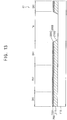
- FIGS. 9 , 10 , 11 , 12 , 13 , and 14 are sectional views describing the method of manufacturing the display device according to one embodiment of the present inventive concept.
- FIGS. 9 to 14 may show a method of manufacturing display devices of FIGS. 5 and 6 .
- a first anti-reflection layer 211 including first metal may be formed on the bottom surface 110L of the substrate 110 having the first region A1 and the second region A2.
- the first anti-reflection layer 211 may be formed on the bottom surface 110L of the substrate 110 by depositing the first metal through sputtering or the like.
- the first metal may include at least one of molybdenum (Mo), aluminum (Al), and titanium (Ti).
- a second anti-reflection layer 221 including molybdenum oxide (MoO x ) and oxide of the second metal other than molybdenum may be formed on the first anti-reflection layer 211.
- the second anti-reflection layer 221 may be formed by depositing molybdenum oxide on the first anti-reflection layer 211 through sputtering or the like and by adding a small amount of the second metal other than molybdenum as an impurity.
- the second metal may include at least one of tantalum (Ta), tungsten (W), niobium (Nb), and copper (Cu).
- the substrate 110 on which the first anti-reflection layer 211 and the second anti-reflection layer 221 is disposed may be cleaned using deionized water (DI water).
- DI water deionized water
- the oxide of the second metal in the second anti-reflection layer 221 may prevent the second anti-reflection layer 221 from being damaged.
- the second anti-reflection layer 221 does not include the oxide of the second metal
- the molybdenum oxide included in the second anti-reflection layer 221 may be dissolved by the deionized water during the cleaning process so that the second anti-reflection layer 221 may be damaged.
- the second anti-reflection layer 221 includes the oxide of the second metal, the damage to the second anti-reflection layer 221 during the cleaning process may be prevented.
- the first anti-reflection layer 211 and the second anti-reflection layer 221 are etched using a photoresist pattern as a mask so that the anti-reflection layer 200 including the first anti-reflection pattern 210 and the second anti-reflection pattern 220 may be formed corresponding to the first region A1.
- the photoresist pattern overlapping the first pixel region PA1 and the first peripheral region SA1 may be formed on the second anti-reflection layer 221, and the second anti-reflection layer 221 and the first anti-reflection layer 211 may be sequentially etched using the photoresist pattern as an etching mask so that the anti-reflection layer 200 overlapping the first pixel region PA1 and the first peripheral region SA1 may be formed.
- the etching process parts of the first anti-reflection layer 211 and the second anti-reflection layer 221 overlapping the second region A2 and the transmission region TA of the first area A1 may be removed.
- the first anti-reflection layer 211 and the second anti-reflection layer 221 may be etched through a dry etching. Since the anti-reflection layer 200 is formed to overlap the first pixel region PA1 and the first peripheral region SA1 of the first region A1, and not to overlap the transmission region TA of the first region A1 and the second region A2, the anti-reflection layer 200 may not be formed by attaching a film having openings in areas corresponding to the transmission region TA of the first region A1 and the second region A2 on the substrate 110.
- the second anti-reflection layer 221 includes an organic material
- the first anti-reflection layer 211 and the second anti-reflection layer 221 have different etching properties, two separate etching processes (a first etching process for etching the second anti-reflection layer 221 and a second etching process for etching the first anti-reflection layer 211) may be required.
- the second anti-reflection layer 221 includes an organic material, it may be difficult to form the second anti-reflection pattern 220 having a relatively small width.
- the anti-reflection layer 200 corresponding to the first region A1 having a relatively small area may be formed through the single etching process. Accordingly, the cost and time for forming the anti-reflection layer 200 can be reduced.
- Molybdenum may be coated with metal oxide including molybdenum oxide (MoO x ) and tantalum oxide (TaO y ) and having a thickness of about 40 nm [400 ⁇ ] to about 65 nm [650 ⁇ ]. Then, the average reflectivity of the coating structure with respect to visible light and the reflectivity of the coating structure with respect to light having 550 nm wavelength were simulated using a software tool, wherein x is the composition ratio of oxygen atoms to molybdenum atoms, y is the composition ratio of oxygen atoms to tantalum atoms, and x and y may be stoichiometrically set as proper values. For example, the composition ratio of tantalum atoms to molybdenum atoms may be set in the range of about 2% to about 6%.
- FIG. 15 is a graph showing a reflectivity simulation result.
- the optimal reflectivity reduction effect is exhibited when the thickness of the metal oxide is in the range of about 45 nm [450 ⁇ ] to about 75 nm [750 ⁇ ].
- a reflectivity reduction effect may be added due to a refractive index matching layer or the like, and accordingly, the reflectivity of less than about 10% may be expected with respect to the light having wavelength of 55 nm [550 ⁇ ].
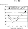
- a molybdenum layer having a thickness of about 250 nm [2500 ⁇ ] may be coated with the metal oxide of Experimental Example 1 having a thickness of about 35 nm [350 ⁇ ] to about 75 nm [750 ⁇ ]. Then, the average reflectivity of the coating structure with respect to the visible light and the reflectivity of the coating structure with respect to the light having 550 nm wavelength may be measured.
- a composition of each element may be analyzed by using energy dispersive X-ray spectroscopy (EDS), x-ray photoelectron spectroscopy (XPS), secondary ion mass spectroscopy (SIMS), auger electron spectroscopy (AES), or the like.
- FIG. 16 is a graph showing a reflectivity measurement result.
- the optimal reflectivity reduction effect is exhibited when the thickness of the metal oxide is in the range of about 35 nm [350 ⁇ ] to about 60 nm [600 ⁇ ].
- the change in reflectivity according to the thickness is similar to the simulation result.
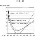
- the metal oxide of Experimental Example 1 may be coated on each of a molybdenum layer, an aluminum layer, and a titanium/aluminum/titanium multilayer to have a thickness of about 45 nm [450 ⁇ ]. Then, each reflectivity of coating structures may be measured according to a wavelength.
- FIG. 17 is a graph showing a reflectivity measurement result.
- the reflectivity reduction effect may increase as a wavelength of light approaches about 550 nm which is the most sensitive wavelength to a human eye.
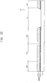
- FIGS. 18 , 19 and 20 are sectional views describing the method of manufacturing the display device according to one embodiment of the present inventive concept.
- FIGS. 18 to 20 may show a method of manufacturing the display device of FIG. 8 .
- a second anti-reflection layer 2221 including molybdenum oxide (MoO x ) and oxide of the second metal other than molybdenum may be formed on the top surface 110U of the substrate 110 having the first region A1 and the second region.
- the second anti-reflection layer 2221 may be formed by depositing molybdenum oxide on the top surface 110U of the substrate 110 through sputtering or the like and by adding a small amount of the second metal as an impurity.
- the first anti-reflection layer 2211 including the first metal may be formed on the second anti-reflection layer 2221.
- the first anti-reflection layer 2211 may be formed by depositing the first metal on the second anti-reflection layer 2221 through sputtering or the like.
- the substrate 110 including the second anti-reflection layer 2221 and the first anti-reflection layer 2211 may be cleaned using deionized water (DI water).
- DI water deionized water
- the first anti-reflection layer 2211 and the second anti-reflection layer 2221 are etched through a single dry etching process using one mask to form the second anti-reflection pattern 2220 and the first anti-reflection pattern 2210 in areas corresponding to the first region A1 may be formed.
- the etching process parts of the second anti-reflection layer 2221 and the first anti-reflection layer 2211 overlapping the second region A2 and the transmission region TA of the first area A1 may be removed.
- the second anti-reflection layer 2221 and the first anti-reflection layer 2211 may be etched through a dry etching.
- the display device may be applied to a display device included in a computer, a notebook, a mobile phone, a smartphone, a smart pad, a PMP, a PDA, an MP3 player, or the like.
Landscapes
- Physics & Mathematics (AREA)
- Optics & Photonics (AREA)
- Engineering & Computer Science (AREA)
- Chemical & Material Sciences (AREA)
- Inorganic Chemistry (AREA)
- Geometry (AREA)
- Microelectronics & Electronic Packaging (AREA)
- General Physics & Mathematics (AREA)
- Manufacturing & Machinery (AREA)
- Electroluminescent Light Sources (AREA)
- Devices For Indicating Variable Information By Combining Individual Elements (AREA)
Abstract
Description
- A display device may provide visual information to a user by displaying an image. To this end, the display device may include a display panel for converting an electrical signal into an image. The display panel may include a light transmission region through which external light incident to the display device transmits. Through the light transmission region, functional modules such as a camera module and a sensor module disposed on a rear side of the display panel may detect or recognize an object and a user positioned in front of the display panel.
- When external light passes through a light transmission region having a relatively small area and is incident onto the functional modules, light interference may occur, and when the interfered external light is reflected by the display panel and/or the functional modules, the user may visually recognize a ghost image or the like in the light transmission region. Accordingly, a method for reducing or substantially preventing the external light reflection in the transmission region is required.
- Embodiments provide a display device in which external light reflection is reduced.
- A display device according to one embodiment may include a display panel having a first region and a second region having a transmittance lower than a transmittance of the first region, the display panel including a substrate and a pixel layer disposed on the substrate, and an anti-reflection layer disposed on one side of the substrate in an area corresponding to the first region. The anti-reflection layer may include a first anti-reflection pattern including first metal and a second anti-reflection pattern disposed on the first anti-reflection pattern and including molybdenum oxide (MoOx) and oxide of second metal other than molybdenum.
- In one embodiment, the anti-reflection layer may overlap the first region and does not overlap the second region.
- In one embodiment, the first metal may include at least one of molybdenum (Mo), aluminum (Al), and titanium (Ti).
- In one embodiment, the second metal may include at least one of tantalum (Ta), tungsten (W), niobium (Nb), and copper (Cu).
- In one embodiment, a ratio of the second metal to molybdenum in the second anti-reflection pattern may be greater than 0 at.% and less than about 20 at.%.
- In one embodiment, the molybdenum oxide included in the second anti-reflection pattern and the oxide of the second metal may have a crystalline structure.
- In one embodiment, the anti-reflection layer may be disposed on a bottom surface of the substrate, and the first anti-reflection pattern may be disposed between the substrate and the second anti-reflection pattern.
- In one embodiment, the anti-reflection layer may be disposed on a top surface of the substrate, and the second anti-reflection pattern may be disposed between the substrate and the first anti-reflection pattern.
- In one embodiment, the second anti-reflection pattern may have a thickness greater than about 10 nm [100 Å] and smaller than about 100 nm [1000 Å].
- In one embodiment, a side-wall of the anti-reflection layer may be inclined with respect to the substrate.
- In one embodiment, the second anti-reflection pattern may have a reflectivity less than a reflectivity of the first anti-reflection pattern.
- In one embodiment, the first region may include a first pixel region, a transmission region, and a first peripheral region surrounding the first pixel region and the transmission region.
- In one embodiment, the anti-reflection layer may overlap the first pixel region and the first peripheral region and may not overlap the transmission region.
- In one embodiment, the second region may include a second pixel region and a second peripheral region surrounding the second pixel region.
- In one embodiment, the second region may surround at least a part of the first region.
- In one embodiment, the display device may further include a functional module disposed under the display panel in an area corresponding to the first region.
- In one embodiment, the functional module may include at least one of a camera module, a face recognition sensor module, a pupil recognition sensor module, an acceleration sensor module, a proximity sensor module, an infrared sensor module, and an illuminance sensor module.
- A method of manufacturing a display device according to one embodiment may include forming a first anti-reflection layer including first metal on a substrate having a first region and a second region that has a transmittance lower than the first region, forming a second anti-reflection layer including molybdenum oxide (MoOx) and oxide of second metal other than molybdenum, and forming an anti-reflection layer in an area corresponding to the first region of the display panel by etching the first anti-reflection layer and the second anti-reflection layer through a single etching process using one mask.
- In one embodiment, the first anti-reflection layer and the second anti-reflection layer may be etched through a dry etching.
- In one embodiment, the method may further include cleaning the substrate including the first anti-reflection layer and the second anti-reflection layer by deionized water, before etching the first anti-reflection layer and the second anti-reflection layer.
- The display device according to the embodiments may include the anti-reflection layer disposed on one side of the substrate corresponding to the first region and including the first anti-reflection pattern including first metal and the second anti-reflection pattern including molybdenum oxide (MoOx) and oxide of second metal other than molybdenum so that the reflection of the external light passing through the first region may be reduced or substantially prevented. Accordingly, ghost image due to interference and reflection of the external light in the first region may not be recognized.
- Illustrative, non-limiting embodiments will be more clearly understood from the following detailed description taken in conjunction with the accompanying drawings.
-
FIG. 1 is a plan view showing a part of a display device according to one embodiment of the present inventive concept. -
FIG. 2 is a sectional view showing one example taken along line I-I' ofFIG. 1 . -
FIG. 3 is a plan view showing a first region of the display device ofFIG. 1 . -
FIG. 4 is a plan view showing a second region of the display device ofFIG. 1 . -
FIG. 5 is a sectional view taken along line II-II' ofFIG. 3 . -
FIG. 6 is a sectional view taken along line III-III' ofFIG. 4 . -
FIG. 7 is a sectional view showing one example taken along line I-I' ofFIG. 1 . -
FIG. 8 is a sectional view showing the display device according to one embodiment of the present inventive concept. -
FIGS. 9 ,10 ,11 ,12 ,13 , and14 are sectional views describing a method of manufacturing the display device according to one embodiment of the present inventive concept. -
FIG. 15 is a graph showing a reflectivity simulation result. -
FIG. 16 is a graph showing a reflectivity measurement result. -
FIG. 17 is a graph showing a reflectivity measurement result. -
FIGS. 18 ,19 and20 are sectional views describing a method of manufacturing the display device according to one embodiment of the present inventive concept. - Hereinafter, display devices and methods of manufacturing display devices in accordance with embodiments will be explained in detail with reference to the accompanying drawings.
- Hereinafter, a display device according to one embodiment will be described with reference to
FIGS. 1 to 6 . -
FIG. 1 is a plan view showing a part of the display device according to one embodiment of the present inventive concept.FIG. 2 is a sectional view showing one example taken along line I-I' ofFIG. 1 . - Referring to
FIGS. 1 and 2 , the display device may include adisplay panel 100, ananti-reflection layer 200, and afunctional module 300. - The
display panel 100 may have a first region A1 and a second region A2. Each of the first region A1 and the second region A2 may be a display region for displaying an image. The first region A1 may include a transmission region for allowing external light to be transmitted therethrough. When the first region A1 includes the transmission region, the transmittance of the first region A1 may be higher than the transmittance of the second region A2. In other words, the transmittance of the second region A2 may be lower than the transmittance of the first region A1. The first region A1 may allow the external light to be transmitted therethrough while displaying the image. - The first region A1 and the second region A2 may be disposed adjacent to each other. In one embodiment, the second region A2 may surround at least a part of the first region A1. For example, the first region A1 may be spaced apart from an edge of the
display panel 100 and disposed in thedisplay panel 100 when viewed from the top, and the second region A2 may completely surround the first region A1. - In one embodiment, the first region A1 may have a circular shape when viewed from the top. However, the present inventive concept is not limited thereto. In another embodiment, the first region A1 may have various polygonal shapes when viewed from the top.
- The
display panel 100 may include asubstrate 110 and a pixel layer DP. The pixel layer DP may be disposed on thesubstrate 110. The pixel layer DP may include pixels for displaying the image. - The
anti-reflection layer 200 may be disposed on thebottom surface 110L of thesubstrate 110 corresponding to the first region A1. Theanti-reflection layer 200 may reduce or substantially prevent the external light incident to the first region A1 from being reflected from thebottom surface 110L or interfaces between adjacent layers that form the pixel layer in the first region A1. - In one embodiment, the
anti-reflection layer 200 may overlap the first region A1 and may not overlap the second region A2. In other words, theanti-reflection layer 200 may be disposed only on thebottom surface 110L of thesubstrate 110 corresponding to the first region A1, and may not be disposed on thebottom surface 110L of thesubstrate 110 corresponding to the second region A2. The first region A1 may completely overlap with theanti-reflection layer 200 in a plan view. - The
anti-reflection layer 200 may include a firstanti-reflection pattern 210 and a secondanti-reflection pattern 220. The secondanti-reflection pattern 220 may be disposed on the firstanti-reflection pattern 210. - In one embodiment, the first
anti-reflection pattern 210 may be disposed between thesubstrate 110 and the secondanti-reflection pattern 220. For example, the firstanti-reflection pattern 210 may be disposed on abottom surface 110L of thesubstrate 110, and the secondanti-reflection pattern 220 may be disposed on abottom surface 210L of the firstanti-reflection pattern 210. - The first
anti-reflection pattern 210 may include first metal. The first metal may include at least one of molybdenum (Mo), aluminum (Al), and titanium (Ti). The firstanti-reflection pattern 210 may reduce reflection of the external light that is incident through the first region A1. - The second
anti-reflection pattern 220 may include molybdenum oxide (MoOx) and oxide of second metal other than molybdenum (Mo). The second metal may include at least one of tantalum (Ta), tungsten (W), niobium (Nb), and copper (Cu). In one embodiment, the secondanti-reflection pattern 220 may include molybdenum oxide (MoOx) and tantalum oxide (TaOy). The secondanti-reflection pattern 220 may absorb the external light incident through the first region A1, so that the reflection of the external light may be reduced or substantially prevented. - Molybdenum oxide may absorb the external light in the second
anti-reflection pattern 220, thereby functioning to reduce the reflectivity of the secondanti-reflection pattern 220. When the secondanti-reflection pattern 220 includes molybdenum oxide, the secondanti-reflection pattern 220 may function as a black matrix. - The oxide of the second metal in the second
anti-reflection pattern 220 may serve to prevent a damage to the secondanti-reflection pattern 220. In the process of forming the secondanti-reflection pattern 220, a process of washing the secondanti-reflection pattern 220 by using deionized water (DI water) may be performed. When the secondanti-reflection pattern 220 does not include the oxide of the second metal, the molybdenum oxide included in the secondanti-reflection pattern 220 may be dissolved by the deionized water during the washing process, so that the secondanti-reflection pattern 220 may be damaged. However, when the secondanti-reflection pattern 220 includes the oxide of the second metal, the secondanti-reflection pattern 220 may not be dissolved by the deionized water, and the damage to the secondanti-reflection pattern 220 during the washing process may be prevented. - In one embodiment, the ratio of the second metal to molybdenum (Mo) in the second
anti-reflection pattern 220 may be greater than 0 at.% and less than about 20 at.%. When the ratio of the second metal to molybdenum (Mo) in the secondanti-reflection pattern 220 is 0 at.%, the secondanti-reflection pattern 220 may be damaged in the process of the washing the secondanti-reflection pattern 220 as described above. When the ratio of the second metal to molybdenum (Mo) in the secondanti-reflection pattern 220 is greater than about 20 at.%, the reflectivity of the secondanti-reflection pattern 220 may exceed a predetermined reflectivity (for example, about 20%). In addition, when the ratio of the second metal to molybdenum (Mo) in the secondanti-reflection pattern 220 is greater than about 20 at.%, the etching properties of the secondanti-reflection pattern 220 may be deteriorated. - The reflectivity of the second
anti-reflection pattern 220 may be smaller than the reflectivity of the firstanti-reflection pattern 210. When theanti-reflection layer 200 includes only the firstanti-reflection pattern 210, theanti-reflection layer 200 may not sufficiently reduce the reflection of the external light incident through the first region A1. However, when thesecond anti-reflection layer 220 having the reflectivity smaller than that of the firstanti-reflection pattern 210 is disposed on the firstanti-reflection pattern 210 , the reflection of the external light incident through the first region A1 may be sufficiently reduced or substantially prevented. - The
functional module 300 may be disposed under thedisplay panel 100 in an area corresponding to the first region A1. In one embodiment, thefunctional module 300 may be disposed on thebottom surface 200L of theanti-reflection layer 200 in an area corresponding to the first region A1. Thefunctional module 300 may receive the external light passing through the first region A1. - In one embodiment, the
functional module 300 may include a camera module configured to photograph (or recognize) an image of the object positioned in front of the display device, a face recognition sensor module configured to sense a face of a user, a pupil recognition sensor module configured to sense a pupil of the user, an acceleration sensor module and a geomagnetic sensor module configured to determine a movement of the display device, a proximity sensor module and an infrared sensor module configured to detect a proximity to a front of the display device, and an illuminance sensor module configured to measure an external brightness. - When the external light passes through the first region A1 having a relatively small area a light interference may occur, and when the interfered external light is reflected by the
display panel 100 and/or thefunctional module 300, the user may visually recognize a ghost image or the like displayed in the first region A1. However, the display device according to one embodiment of the present inventive concept includes theanti-reflection layer 200 disposed on thebottom surface 110L of thesubstrate 110 in the area corresponding to the first region A1, and thus theanti-reflection layer 200 may absorb the external light even when the light interference occurs from the external light passing through the first region A1, so that the reflection of the external light may be reduced or substantially prevented. Accordingly, the user may be prevented from visually recognizing the ghost image or the like. -
FIG. 3 is a plan view showing the first region A1 of the display device ofFIG. 1 .FIG. 4 is a plan view showing the second region A2 of the display device ofFIG. 1 . - Referring to
FIGS. 1 ,3 and 4 , the first region A1 may include a first pixel region PA1, a transmission region TA, and a first peripheral region SA1, and the second region A2 may include a second pixel region PA2 and a second peripheral region SA2. Each of the first pixel region PA1 and the second pixel region PA2 may be a region in which pixels are disposed to emit light generated from each of the pixels thereby displaying an image. - The first pixel region PA1 may include a plurality of first sub-pixel regions SRA1, SGA1, and SBA1 emitting light having mutually different colors, and the second pixel region PA2 may include a plurality of second sub-pixel regions SRA2, SGA2, and SBA2 emitting light having mutually different colors. In one embodiment, the sub-pixel regions SRA1, SGA1, and SBA1 may include a first red pixel region SRA1 emitting red light, a first green pixel region SGA1 emitting green light, and a first blue pixel region SBA1 emitting blue light, and the second sub-pixel regions SRA2, SGA2, and SBA2 may include a second red pixel region SRA2 emitting red light, a second green pixel region SGA2 emitting green light, and a second blue pixel region SBA2 emitting blue light.
- The transmission region TA may be a region in which no sub-pixels is disposed and that transmits the external light incident to the
display panel 100. When the first region A1 includes the transmission region TA through which the external light is transmitted, thefunctional module 300 disposed under thedisplay panel 100 in the area corresponding to the first region A1 may easily detect or recognize the object or the user positioned in front of the display device through the transmission region TA. The first peripheral region SA1 may surround the first pixel region PA1 and the transmission region TA. The second peripheral region SA2 may surround the second pixel area PA2. Each of the first peripheral region SA1 and the second peripheral region SA2 may be a region in which light is not emitted and external light is not transmitted. - When the first region A1 includes the transmission region TA, the number of first sub-pixel regions SRA1, SGA1, and SBA1 per unit area may be smaller than the number of second sub-pixel regions SRA2, SGA2, and SBA2 per unit area in the second region A2. In other words, a resolution of the first region A1 may be less than a resolution of the second region A2.
- In one embodiment, an arrangement structure of the first sub-pixel regions SRA1, SGA1, and SBA1 the first region A1 may be different from an arrangement structure of the second sub-pixel regions SRA2, SGA2, and SBA2 the second region A2. For example, the first sub-pixel regions SRA1, SGA1, and SBA1 may be arranged in a stripe manner, and the second sub-pixel regions SRA2, SGA2, and SBA2 may be arranged in a PenTile manner. In this case, the first pixel region PA1 may include one first red pixel region SRA1, one first green pixel region SGA1, and one first blue pixel region SBA1, and the second pixel region PA2 may include one second red pixel region SRA2, two second green pixel regions SGA2, and one second blue pixel region SBA2.
-
FIG. 5 is a sectional view taken along line II-II' ofFIG. 3 .FIG. 6 is a sectional view taken along line III-III' ofFIG. 4 . - Referring to
FIGS. 5 and6 , thedisplay panel 100 may include asubstrate 110 and a pixel layer DP. The pixel layer DP may include anactive layer 120, a plurality ofconductive layers layers layer 113, afirst electrode 150, apixel defining layer 114, alight emitting layer 160, asecond electrode 170, and anencapsulation layer 180. - The
substrate 110 may be a transparent insulating substrate. For example, thesubstrate 110 may be formed of glass, quartz, plastic, or the like. - The
active layer 120 may be disposed on thesubstrate 110. Theconductive layers substrate 110 on different layers. Theconductive layers gate electrode 130, asource electrode 141, and adrain electrode 142. Theactive layer 120 and theconductive layers - The inorganic insulating
layers active layer 120 and theconductive layers substrate 110. The inorganic insulatinglayers gate insulating layer 111 and an interlayer insulatinglayer 112. - The
active layer 120 may be disposed on thesubstrate 110. Theactive layer 120 may be formed of amorphous silicon, polycrystalline silicon, oxide semiconductor, or the like. Theactive layer 120 may include a source region, a drain region, and a channel region disposed between the source region and the drain region. P-type or N-type impurities may be doped in the source region and the drain region, and impurities may not be doped in the channel region. - The
gate insulating layer 111 may be disposed on theactive layer 120. Thegate insulating layer 111 may be formed on thesubstrate 110 while covering theactive layer 120. Thegate insulating layer 111 may insulate thegate electrode 130 from theactive layer 120. Thegate insulating layer 111 may be formed of an inorganic insulating material such as silicon nitride, and silicon oxide, silicon oxynitride. - The
gate electrode 130 may be disposed on thegate insulating layer 111. Thegate electrode 130 may overlap the channel region of theactive layer 120. Thegate electrode 130 may be formed of a conductive material such as metal or a metal alloy. For example, thegate electrode 130 may be formed of molybdenum (Mo), copper (Cu), and the like. - An interlayer insulating
layer 112 may be disposed on thegate electrode 130. The interlayer insulatinglayer 112 may be formed on thegate insulating layer 111 while covering thegate electrode 130. The interlayer insulatinglayer 112 may insulate thesource electrode 141 and thedrain electrode 142 from thegate electrode 130. The interlayer insulatinglayer 112 may be formed of an inorganic insulating material such as silicon nitride, and silicon oxide, silicon oxynitride. - The
source electrode 141 and thedrain electrode 142 may be disposed on theinterlayer insulating layer 112. Thesource electrode 141 may be connected to the source region of theactive layer 120, and thedrain electrode 142 may be connected to the drain region of theactive layer 120. Thesource electrode 141 and thedrain electrode 142 may be formed of a conductive material such as metal or a metal alloy. For example, thesource electrode 141 and thedrain electrode 142 may be formed of aluminum (Al), titanium (Ti), copper (Cu), or the like. Theactive layer 120, thegate electrode 130, thesource electrode 141, and thedrain electrode 142 may form a transistor TR. The transistor TR may be disposed in the first pixel region PA1 and the second pixel region PA2. - The organic insulating
layer 113 may be disposed on thesource electrode 141 and thedrain electrode 142. The organic insulatinglayer 113 may be formed on theinterlayer insulating layer 112 while covering thesource electrode 141 and thedrain electrode 142. The organic insulatinglayer 113 may protect the transistor TR and may provide a flat surface onto an upper portion of the transistor TR. The organic insulatinglayer 113 may be formed of an organic insulating material such as polyimide (PI). - The
first electrode 150 may be disposed on the organic insulatinglayer 113. Thefirst electrode 150 may be connected to thedrain electrode 142. Thefirst electrode 150 may be disposed in the first pixel region PA1 and the second pixel region PA2. Thefirst electrode 150 may be formed of a conductive material such as metal or transparent conductive oxide. - The
pixel defining layer 114 may be disposed on thefirst electrode 150. Thepixel defining layer 114 may define the first pixel region PA1 and the second pixel region PA2 while including a pixel opening exposing at least a center of thefirst electrode 150. In addition, thepixel defining layer 114 may separate thesecond electrode 170 from an edge of thefirst electrode 150 in a thickness direction, so that an arc or the like may be prevented from occurring between thesecond electrode 170 and the edge of thefirst electrode 150. Thepixel defining layer 114 may be formed of an organic insulating material such as polyimide (PI). - The
light emitting layer 160 may be disposed on thefirst electrode 150. Thelight emitting layer 160 may be disposed on thefirst electrode 150 exposed by the pixel opening. Thelight emitting layer 160 may include at least one of an organic light emitting material and a quantum dot. - In one embodiment, the organic light emitting material may include a low molecular organic compound or a high molecular organic compound. For example, the low molecular organic compound may include copper phthalocyanine, N,N'-diphenylbenzidine, tris-(8-hydroxyquinoline)aluminum, and the like, and the high molecular organic compound may include poly(3,4-ethylenedioxythiophene, polyaniline, poly-phenylenevinylene, polyfluorene, and the like.
- In one embodiment, the quantum dot may include a core including a group II-VI compound, a group III-V compound, a group IV-VI compound, a group IV element, a group IV compound, and a combination thereof. In one embodiment, the quantum dot may have a core-shell structure including a core and a shell surrounding the core. The shell may prevent chemical denaturation of the core, thereby serving as a protective layer for maintaining semiconductor properties and as a charging layer for imparting electrophoretic properties to the quantum dots.
- The
second electrode 170 may be disposed on thelight emitting layer 160. Thesecond electrode 170 may also be disposed on thepixel defining layer 114. Thesecond electrode 170 may face thefirst electrode 150 with thelight emitting layer 160 interposed therebetween. Thesecond electrode 170 may be formed of a conductive material such as metal or transparent conductive oxide. Thefirst electrode 150, thelight emitting layer 160, and thesecond electrode 170 may form a light emitting element EL. The light emitting element EL may be disposed in the first pixel region PA1 and the second pixel region PA2. - The
display panel 100 may include a transmission window TW overlapping the transmission region TA. The transmission window TW may be defined as openings of components of thedisplay panel 100 overlapping the transmission region TA. At least one of thegate insulating layer 111, theinterlayer insulating layer 112, the organic insulatinglayer 113, thepixel defining layer 114, and thesecond electrode 170 may have an opening overlapping the transmission region TA. - In one embodiment, the
second electrode 170, thepixel defining layer 114, the organic insulatinglayer 113, theinterlayer insulating layer 112, and thegate insulating layer 111 may have a first opening OP1, a second opening OP2, a third opening OP3, a fourth opening OP4, and a fifth opening OP5 that overlap the transmission region TA, respectively. In this case, the first opening OP1 of thesecond electrode 170, the second opening OP2 of thepixel defining layer 114, the third opening OP3 of the organic insulatinglayer 113, the fourth opening OP4 of the interlayer insulatinglayer 112, and the fifth opening OP5 of thegate insulating layer 111 may form the transmission window TW. - When the insulating layers are laminated in the transmission region TA, the reflectivity of external light reflected at interfaces between adjacent insulating layers may increase. In addition, when the conductive layer is disposed in the transmission region TA, the reflectivity of external light by the conductive layer may increase. However, the
display panel 100 according to embodiments of the present inventive concept includes the transmission window TW overlapping the transmission region TA, so that the number of interfaces between adjacent insulating layers in the transmission region TA may decrease, or an area of the conductive layer disposed in the transmission region TA may decrease. Accordingly, the reflectivity of the external light by the interfaces between the adjacent insulating layers or by the conductive layer may decrease. - The
encapsulation layer 180 may be disposed on thesecond electrode 170. Theencapsulation layer 180 may include at least one inorganic layer and at least one organic layer. - A part of the
encapsulation layer 180 overlapping the first pixel region PA1, the first peripheral region SA1, the second pixel region PA2, and the second peripheral region SA2 may be disposed on the light emitting element EL to block impurities from the outside from being introduced into the light emitting element EL, and protect the light emitting element EL from an external impact. In addition, a part of theencapsulation layer 180 overlapping the transmission region TA may fill the transmission window TW. Theencapsulation layer 180 may have a flat top surface throughout the first pixel region PA1, the first peripheral region SA1, the transmissive region TA, the second pixel region PA2, and the second peripheral region SA2. - In one embodiment, the
encapsulation layer 180 may include a first inorganic layer, a second inorganic layer disposed on the first inorganic layer, and an organic layer disposed between the first inorganic layer and the second inorganic layer. The first inorganic layer and the second inorganic layer may reduce or substantially block impurities such as oxygen and moisture from permeating into the light emitting element EL. The organic layer may improve sealing properties of theencapsulation layer 180, alleviate internal stresses of the first inorganic layer and the second inorganic layer, compensating for defects in the first inorganic layer and the second inorganic layer, and provide a flat top surface onto the second inorganic layer. - The
anti-reflection layer 200 may be disposed on thebottom surface 110L of thesubstrate 110 corresponding to the first region A1. Theanti-reflection layer 200 may overlap the first pixel region PA1 and the first peripheral region SA1, and may not overlap the transmission region TA. When theanti-reflection layer 200 overlaps the first pixel region PA1 and the first peripheral region SA1, the external light incident to the first region A1 may be reduced or substantially prevented from being reflected from the first pixel region PA1 and the first peripheral region SA1. In addition, when theanti-reflection layer 200 does not overlap the transmission region TA, the external light passing through the transmission region TA of the first region A1 may be prevented from being blocked by theanti-reflection layer 200. - A
sidewall 200S of theanti-reflection layer 200 may be inclined with respect to thesubstrate 100. For example, thesidewall 200S of theanti-reflection layer 200 may include asidewall 210S of the firstanti-reflection pattern 210 and asidewall 220S of the secondanti-reflection pattern 220, and each of thesidewall 210S of the firstanti-reflection pattern 210 and thesidewall 220S of the secondanti-reflection pattern 220 may be inclined at an angle smaller than about 90 degrees with respect to thebottom surface 110L of thesubstrate 100. - In one embodiment, as shown in
FIG. 5 , thesidewall 220S of the secondanti-reflection pattern 220 may come into contact with thesidewall 210S of the firstanti-reflection pattern 210. In other words, thesidewall 200S of theanti-reflection layer 200 which includes thesidewall 210S of the firstanti-reflection pattern 210 and thesidewall 220S of the secondanti-reflection pattern 220 may be disposed on a straight line. For example, a width of a top surface of the secondanti-reflection pattern 220 may be substantially the same as a width of a bottom surface of the firstanti-reflection pattern 210. - In another embodiment, the
sidewall 220S of the secondanti-reflection pattern 220 may be spaced apart from thesidewall 210S of the firstanti-reflection pattern 210. In other words, thesidewall 200S of theanti-reflection layer 200 may have a stepped structure. For example, thesidewall 220S of the secondanti-reflection pattern 220 may protrude or be recessed from thesidewall 210S of the firstanti-reflection pattern 210. - In one embodiment, a
thickness 210T of the firstanti-reflection pattern 210 may be greater than about 100 nm [1000 Å] and less than about 400 nm [4000 Å]. For example, when the firstanti-reflection pattern 210 includes molybdenum, thethickness 210T of the firstanti-reflection pattern 210 may be about 250 nm [2500 Å]. - In one embodiment, a
thickness 220T of the secondanti-reflection pattern 220 may be greater than about 10 nm [100 Å] and less than about 100 nm [1000 Å]. When thethickness 220T of the secondanti-reflection pattern 220 is less than about 10 nm [100 Å] or greater than about 100 nm [1000 Å], the reflectivity of the first pixel region PA1 and the first peripheral region SA1 may exceed a predetermined reflectivity (e.g., about 20%), so that the reflection of the external light in the first region A1 may increase. - In one embodiment, the molybdenum oxide included in the second
anti-reflection pattern 220 and the oxide of the second metal may have a crystalline structure. The molybdenum oxide and the oxide of the second metal having an amorphous structure may be deposited to form the secondanti-reflection pattern 220. The amorphous molybdenum oxide and the amorphous oxide of the second metal may be crystallized during a process of forming the transistor TR that includes a heat treatment process at a temperature of about 300°C or higher so that the secondanti-reflection pattern 220 may include the crystalline molybdenum oxide and the crystalline oxide of the second metal. However, the present inventive concept is not limited thereto. In another embodiment, when the heat treatment process does not proceed, the molybdenum oxide and the oxide of the second metal included in the secondanti-reflection pattern 220 may have an amorphous structure. - Hereinafter, a display device according to another embodiment will be described with reference to
FIG. 7 . In regard to the display device described with reference toFIG. 7 , duplicate descriptions for components substantially the same as or similar to the display device described with reference toFIGS. 1 to 6 will be omitted. -
FIG. 7 is a sectional view showing one example taken along line I-I' ofFIG. 1 . - Referring to
FIG. 7 , the display device may include adisplay panel 100, an anti-reflection layer 1200, and afunctional module 300. - The anti-reflection layer 1200 may be disposed on the
bottom surface 110L of thesubstrate 110 corresponding to the first region A1. The anti-reflection layer 1200 may include afirst anti-reflection pattern 1210 and a second anti-reflection pattern 1220. The second anti-reflection pattern 1220 may be disposed on thefirst anti-reflection pattern 1210. - In one embodiment, the second anti-reflection pattern 1220 may be disposed between the
substrate 110 and thefirst anti-reflection pattern 1210. For example, the second anti-reflection pattern 1220 may be disposed on abottom surface 110L of thesubstrate 110, and thefirst anti-reflection pattern 1210 may be disposed on abottom surface 1220L of the second anti-reflection pattern 1220. - Hereinafter, a display device according to a still another embodiment will be described with reference to
FIG. 8 . In regard to the display device described with reference toFIG. 8 , duplicate descriptions for components substantially the same as or similar to the display device described with reference toFIGS. 1 to 6 will be omitted. -
FIG. 8 is a sectional view showing the display device according to one embodiment of the present inventive concept.FIG. 8 may show the first region A1 ofFIG. 1 . - Referring to
FIG. 8 , thedisplay panel 100 may include asubstrate 110 and a pixel layer DP. The pixel layer DP may include a buffer layer BUF, anactive layer 120, a plurality ofconductive layers layers layer 113, afirst electrode 150, apixel defining layer 114, alight emitting layer 160, asecond electrode 170, and anencapsulation layer 180. - An
anti-reflection layer 2200 may be disposed on atop surface 110U of thesubstrate 110 corresponding to the first region A1. Theanti-reflection layer 2200 may overlap the first pixel region PA1 and the first peripheral region SA1, and may not overlap the transmission region TA. Theanti-reflection layer 2200 may include afirst anti-reflection pattern 2210 and asecond anti-reflection pattern 2220. Thesecond anti-reflection pattern 2220 may be disposed on thefirst anti-reflection pattern 2210. - In one embodiment, the
second anti-reflection pattern 2220 may be disposed between thesubstrate 110 and thefirst anti-reflection pattern 2210. For example, thesecond anti-reflection pattern 2220 may be disposed on thetop surface 110U of thesubstrate 110, and thefirst anti-reflection pattern 2210 may be disposed on a top surface of thesecond anti-reflection pattern 2220. However, the present inventive concept is not limited thereto. In another embodiment, thefirst anti-reflection pattern 2210 may be disposed between thesubstrate 110 and thesecond anti-reflection pattern 2220. Thefirst anti-reflection pattern 2210 and thesecond anti-reflection pattern 2220 may be formed of the same material as the firstanti-reflection pattern 210 and the secondanti-reflection pattern 220 as described according toFIGS. 1 through 5 , respectively. - The buffer layer BUF may be disposed on the
anti-reflection layer 2200. The buffer layer BUF may be formed on thesubstrate 110 while covering theanti-reflection layer 2200. The buffer layer BUF may insulate theactive layer 111 from theanti-reflection layer 2200. The buffer layer BUF may be formed of an inorganic insulating material such as silicon nitride, and silicon oxide, silicon oxynitride. - The
display panel 100 may include a transmission window TW overlapping the transmission region TA. At least one of the buffer layer BUF, thegate insulating layer 111, theinterlayer insulating layer 112, the organic insulatinglayer 113, thepixel defining layer 114, and thesecond electrode 170 may have an opening overlapping the transmission region TA. - In one embodiment, the
second electrode 170, thepixel defining layer 114, the organic insulatinglayer 113, theinterlayer insulating layer 112, thegate insulating layer 111, the buffer layer BUF may have a first opening OP1, a second opening OP2, a third opening OP3, a fourth opening OP4, a fifth opening OP5, and a sixth opening OP6 that overlap the transmission region TA, respectively. In this case, the first opening OP1 of thesecond electrode 170, the second opening OP2 of thepixel defining layer 114, the third opening OP3 of the organic insulatinglayer 113, the fourth opening OP4 of the interlayer insulatinglayer 112, the fifth opening OP5 of thegate insulating layer 111, and the sixth opening OP6 of the buffer layer BUF may form the transmission window TW. - Hereinafter, a method of manufacturing a display device according to one embodiment will be described with reference to
FIGS. 9 to 14 . -
FIGS. 9 ,10 ,11 ,12 ,13 , and14 are sectional views describing the method of manufacturing the display device according to one embodiment of the present inventive concept. For example,FIGS. 9 to 14 may show a method of manufacturing display devices ofFIGS. 5 and6 . - Referring to
FIGS. 9 and10 , afirst anti-reflection layer 211 including first metal may be formed on thebottom surface 110L of thesubstrate 110 having the first region A1 and the second region A2. For example, thefirst anti-reflection layer 211 may be formed on thebottom surface 110L of thesubstrate 110 by depositing the first metal through sputtering or the like. The first metal may include at least one of molybdenum (Mo), aluminum (Al), and titanium (Ti). - Referring to
FIGS. 11 and12 , asecond anti-reflection layer 221 including molybdenum oxide (MoOx) and oxide of the second metal other than molybdenum may be formed on thefirst anti-reflection layer 211. For example, thesecond anti-reflection layer 221 may be formed by depositing molybdenum oxide on thefirst anti-reflection layer 211 through sputtering or the like and by adding a small amount of the second metal other than molybdenum as an impurity. The second metal may include at least one of tantalum (Ta), tungsten (W), niobium (Nb), and copper (Cu). - In one embodiment, after forming the
second anti-reflection layer 221 and before etching thefirst anti-reflection layer 211 and thesecond anti-reflection layer 221, thesubstrate 110 on which thefirst anti-reflection layer 211 and thesecond anti-reflection layer 221 is disposed may be cleaned using deionized water (DI water). The oxide of the second metal in thesecond anti-reflection layer 221 may prevent thesecond anti-reflection layer 221 from being damaged. When thesecond anti-reflection layer 221 does not include the oxide of the second metal, the molybdenum oxide included in thesecond anti-reflection layer 221 may be dissolved by the deionized water during the cleaning process so that thesecond anti-reflection layer 221 may be damaged. However, when thesecond anti-reflection layer 221 includes the oxide of the second metal, the damage to thesecond anti-reflection layer 221 during the cleaning process may be prevented. - Referring to
FIGS. 13 and14 , thefirst anti-reflection layer 211 and thesecond anti-reflection layer 221 are etched using a photoresist pattern as a mask so that theanti-reflection layer 200 including the firstanti-reflection pattern 210 and the secondanti-reflection pattern 220 may be formed corresponding to the first region A1. For example, the photoresist pattern overlapping the first pixel region PA1 and the first peripheral region SA1 may be formed on thesecond anti-reflection layer 221, and thesecond anti-reflection layer 221 and thefirst anti-reflection layer 211 may be sequentially etched using the photoresist pattern as an etching mask so that theanti-reflection layer 200 overlapping the first pixel region PA1 and the first peripheral region SA1 may be formed. In the etching process, parts of thefirst anti-reflection layer 211 and thesecond anti-reflection layer 221 overlapping the second region A2 and the transmission region TA of the first area A1 may be removed. - In one embodiment, the
first anti-reflection layer 211 and thesecond anti-reflection layer 221 may be etched through a dry etching. Since theanti-reflection layer 200 is formed to overlap the first pixel region PA1 and the first peripheral region SA1 of the first region A1, and not to overlap the transmission region TA of the first region A1 and the second region A2, theanti-reflection layer 200 may not be formed by attaching a film having openings in areas corresponding to the transmission region TA of the first region A1 and the second region A2 on thesubstrate 110. - In a comparative example in which the
second anti-reflection layer 221 includes an organic material, since thefirst anti-reflection layer 211 and thesecond anti-reflection layer 221 have different etching properties, two separate etching processes (a first etching process for etching thesecond anti-reflection layer 221 and a second etching process for etching the first anti-reflection layer 211) may be required. In addition, since thesecond anti-reflection layer 221 includes an organic material, it may be difficult to form the secondanti-reflection pattern 220 having a relatively small width. - However, according to one embodiment of the present inventive concept, because the
first anti-reflection layer 211 and thesecond anti-reflection layer 221 are etched through a single dry etching process using one mask, theanti-reflection layer 200 corresponding to the first region A1 having a relatively small area may be formed through the single etching process. Accordingly, the cost and time for forming theanti-reflection layer 200 can be reduced. - Hereinafter, experimental examples will be described in which the reflectivity of metal coated with the anti-reflection material of the second anti-reflection pattern of the present inventive concept is measured.
- Molybdenum may be coated with metal oxide including molybdenum oxide (MoOx) and tantalum oxide (TaOy) and having a thickness of about 40 nm [400 Å] to about 65 nm [650 Å]. Then, the average reflectivity of the coating structure with respect to visible light and the reflectivity of the coating structure with respect to light having 550 nm wavelength were simulated using a software tool, wherein x is the composition ratio of oxygen atoms to molybdenum atoms, y is the composition ratio of oxygen atoms to tantalum atoms, and x and y may be stoichiometrically set as proper values. For example, the composition ratio of tantalum atoms to molybdenum atoms may be set in the range of about 2% to about 6%.
-
FIG. 15 is a graph showing a reflectivity simulation result. - Referring to
FIG. 15 , it can be seen that the optimal reflectivity reduction effect is exhibited when the thickness of the metal oxide is in the range of about 45 nm [450 Å] to about 75 nm [750 Å]. When the configuration is applied to the display device, a reflectivity reduction effect may be added due to a refractive index matching layer or the like, and accordingly, the reflectivity of less than about 10% may be expected with respect to the light having wavelength of 55 nm [550 Å]. - A molybdenum layer having a thickness of about 250 nm [2500 Å] may be coated with the metal oxide of Experimental Example 1 having a thickness of about 35 nm [350 Å] to about 75 nm [750 Å]. Then, the average reflectivity of the coating structure with respect to the visible light and the reflectivity of the coating structure with respect to the light having 550 nm wavelength may be measured. In metal oxide having the above composition formula, a composition of each element may be analyzed by using energy dispersive X-ray spectroscopy (EDS), x-ray photoelectron spectroscopy (XPS), secondary ion mass spectroscopy (SIMS), auger electron spectroscopy (AES), or the like.
-
FIG. 16 is a graph showing a reflectivity measurement result. - Referring to
FIG. 16 , it can be seen that the optimal reflectivity reduction effect is exhibited when the thickness of the metal oxide is in the range of about 35 nm [350 Å] to about 60 nm [600 Å]. In addition, it can be seen that the change in reflectivity according to the thickness is similar to the simulation result. - The metal oxide of Experimental Example 1 may be coated on each of a molybdenum layer, an aluminum layer, and a titanium/aluminum/titanium multilayer to have a thickness of about 45 nm [450 Å]. Then, each reflectivity of coating structures may be measured according to a wavelength.
-
FIG. 17 is a graph showing a reflectivity measurement result. - Referring to
FIG. 17 , when the metal oxide is coated, the reflectivity reduction effect may increase as a wavelength of light approaches about 550 nm which is the most sensitive wavelength to a human eye. - Hereinafter, a method of manufacturing a display device according to one embodiment will be described with reference to
FIGS. 18 to 20 . -
FIGS. 18 ,19 and20 are sectional views describing the method of manufacturing the display device according to one embodiment of the present inventive concept. For example,FIGS. 18 to 20 may show a method of manufacturing the display device ofFIG. 8 . - Referring to
FIG. 18 , asecond anti-reflection layer 2221 including molybdenum oxide (MoOx) and oxide of the second metal other than molybdenum may be formed on thetop surface 110U of thesubstrate 110 having the first region A1 and the second region. For example, thesecond anti-reflection layer 2221 may be formed by depositing molybdenum oxide on thetop surface 110U of thesubstrate 110 through sputtering or the like and by adding a small amount of the second metal as an impurity. - Referring to
FIG. 19 , thefirst anti-reflection layer 2211 including the first metal may be formed on thesecond anti-reflection layer 2221. For example, thefirst anti-reflection layer 2211 may be formed by depositing the first metal on thesecond anti-reflection layer 2221 through sputtering or the like. - In one embodiment, after forming the
first anti-reflection layer 2211 and before etching thesecond anti-reflection layer 2221 and thefirst anti-reflection layer 2211, thesubstrate 110 including thesecond anti-reflection layer 2221 and thefirst anti-reflection layer 2211 may be cleaned using deionized water (DI water). - Referring to
FIG. 20 , thefirst anti-reflection layer 2211 and thesecond anti-reflection layer 2221 are etched through a single dry etching process using one mask to form thesecond anti-reflection pattern 2220 and thefirst anti-reflection pattern 2210 in areas corresponding to the first region A1 may be formed. In the etching process, parts of thesecond anti-reflection layer 2221 and thefirst anti-reflection layer 2211 overlapping the second region A2 and the transmission region TA of the first area A1 may be removed. In one embodiment, thesecond anti-reflection layer 2221 and thefirst anti-reflection layer 2211 may be etched through a dry etching. - The display device according to the embodiments may be applied to a display device included in a computer, a notebook, a mobile phone, a smartphone, a smart pad, a PMP, a PDA, an MP3 player, or the like.
- Although the display devices and methods of manufacturing the display devices according to the embodiments have been described with reference to the drawings, the illustrated embodiments are examples, and may be modified and changed by a person having ordinary knowledge in the relevant technical field without departing from the technical spirit described in the following claims.
Claims (20)
- A display device comprising:a display panel (100) having a first region (A1) and a second region (A2) having a transmittance lower than a transmittance of the first region (A1), the display panel (100) including a substrate (110) and a pixel layer (DP) disposed on the substrate (110);characterized byan anti-reflection layer (200) disposed on one side of the substrate (110) in an area corresponding to the first region (A1), wherein the anti-reflection layer (200) includes:a first anti-reflection pattern (210) including first metal; anda second anti-reflection pattern (220) disposed on the first anti-reflection pattern (210) and including molybdenum oxide (MoOx) and oxide of second metal other than molybdenum.
- The display device of claim 1, wherein the anti-reflection layer (200) overlaps the first region (A1) and does not overlap the second region (A2).
- The display device of at least one of claims 1 or 2, wherein the first metal includes at least one of molybdenum (Mo), aluminum (Al), and titanium (Ti).
- The display device of at least one of claims 1 to 3, wherein the second metal includes at least one of tantalum (Ta), tungsten (W), niobium (Nb), and copper (Cu).
- The display device of at least one of claims 1 to 4, wherein a ratio of the second metal to molybdenum in the second anti-reflection pattern (220) is greater than 0 at.% and less than about 20 at.%.
- The display device of at least one of claims 1 to 5, wherein the molybdenum oxide included in the second anti-reflection pattern (220) and the oxide of the second metal have a crystalline structure.
- The display device of at least one of claims 1 to 6, wherein the anti-reflection layer (200) is disposed on a bottom surface (110L) of the substrate (110), and the first anti-reflection pattern (210) is disposed between the substrate (110) and the second anti-reflection pattern (220).
- The display device of at least one of claims 1 to 7, wherein the anti-reflection layer (200) is disposed on a top surface (110U) of the substrate (110), and the second anti-reflection pattern (220) is disposed between the substrate (110) and the first anti-reflection pattern (210).
- The display device of at least one of claims 1 to 8, wherein the second anti-reflection pattern (220) has a thickness greater than about 10 nm and smaller than about 100 nm.
- The display device of at least one of claims 1 to 9, wherein a side-wall (210S) of the anti-reflection layer (200) is inclined with respect to the substrate (110).
- The display device of at least one of claims 1 to 10, wherein the second anti-reflection pattern (220) has a reflectivity less than a reflectivity of the first anti-reflection pattern (210).
- The display device of at least one of claims 1 to 11, wherein the first region (A1) includes a first pixel region (PA1), a transmission region (TA), and a first peripheral region (SA1) surrounding the first pixel region (PA1) and the transmission region (TA).
- The display device of claim 12, wherein the anti-reflection layer (200) overlaps the first pixel region (PA1) and the first peripheral region (SA1) and does not overlap the transmission region (TA).
- The display device of at least one of claims 12 or 13, wherein the second region (A2) includes a second pixel region (PA2) and a second peripheral region (SA2) surrounding the second pixel region (PA2).
- The display device of claim 1, wherein the second region (A2) surrounds at least a part of the first region (A1).
- The display device of at least one of claims 1 to 15, further comprising:
a functional module (300) disposed under the display panel (100) in an area corresponding to the first region (A1). - The display device of claim 16, wherein the functional module (300) includes at least one of a camera module, a face recognition sensor module, a pupil recognition sensor module, an acceleration sensor module, a proximity sensor module, an infrared sensor module, and an illuminance sensor module.
- A method of manufacturing a display device, the method comprising:forming a first anti-reflection layer (211) including first metal on a substrate (110) having a first region (A1) and a second region (A2) that has a transmittance lower than the first region (A1);forming a second anti-reflection layer (221) including molybdenum oxide (MoOx) and oxide of second metal other than molybdenum;characterized byforming an anti-reflection layer (200) in an area corresponding to the first region (A1) of the display panel (100) by etching the first anti-reflection layer (211) and the second anti-reflection layer (221) through a single etching process using one mask.
- The method of claim 18, wherein the first anti-reflection layer (211) and the second anti-reflection layer (221) are etched through a dry etching.
- The method of at least one of claims 18 or 19, further comprising:
cleaning the substrate (110) including the first anti-reflection layer (211) and the second anti-reflection layer (221) by deionized water before etching the first anti-reflection layer (211) and the second anti-reflection layer (221).
Applications Claiming Priority (1)
| Application Number | Priority Date | Filing Date | Title |
|---|---|---|---|
| KR1020200050822A KR102811895B1 (en) | 2020-04-27 | 2020-04-27 | Display device and method of manufacturing the same |
Publications (2)
| Publication Number | Publication Date |
|---|---|
| EP3904920A1 true EP3904920A1 (en) | 2021-11-03 |
| EP3904920B1 EP3904920B1 (en) | 2024-05-15 |
Family
ID=74873544
Family Applications (1)
| Application Number | Title | Priority Date | Filing Date |
|---|---|---|---|
| EP21162247.7A Active EP3904920B1 (en) | 2020-04-27 | 2021-03-12 | Display device and method of manufacturing the same |
Country Status (4)
| Country | Link |
|---|---|
| US (1) | US11877474B2 (en) |
| EP (1) | EP3904920B1 (en) |
| KR (1) | KR102811895B1 (en) |
| CN (1) | CN113644215A (en) |
Families Citing this family (6)
| Publication number | Priority date | Publication date | Assignee | Title |
|---|---|---|---|---|
| KR102841198B1 (en) | 2020-07-31 | 2025-07-31 | 삼성디스플레이 주식회사 | Display device |
| KR102883540B1 (en) | 2020-09-15 | 2025-11-10 | 삼성디스플레이 주식회사 | Display device |
| KR102849264B1 (en) | 2020-10-19 | 2025-08-22 | 삼성디스플레이 주식회사 | Display device |
| KR102957052B1 (en) * | 2021-03-18 | 2026-04-24 | 삼성디스플레이 주식회사 | Display device |
| KR102934417B1 (en) * | 2021-12-31 | 2026-03-04 | 엘지디스플레이 주식회사 | Liquid crystal display device |
| CN114914285A (en) * | 2022-05-23 | 2022-08-16 | Oppo广东移动通信有限公司 | Display module and electronic device |
Citations (4)
| Publication number | Priority date | Publication date | Assignee | Title |
|---|---|---|---|---|
| EP1020738A1 (en) * | 1999-01-14 | 2000-07-19 | Sumitomo Chemical Company, Limited | Three-layer anti-reflection filn containing a first layer of binder resin with ultrafine particles |
| US20110019277A1 (en) * | 2007-11-08 | 2011-01-27 | Sager Brian M | anti-reflective coating |
| US20130343032A1 (en) * | 2012-06-20 | 2013-12-26 | Samsung Display Co., Ltd. | Polarization structures, methods of manufacturing polarization structure and display devices including polarization structures |
| WO2018064947A1 (en) * | 2016-10-06 | 2018-04-12 | Hong Kong Baptist University | Sapphire thin film coated substrate |
Family Cites Families (13)
| Publication number | Priority date | Publication date | Assignee | Title |
|---|---|---|---|---|
| JP4166455B2 (en) * | 2001-10-01 | 2008-10-15 | 株式会社半導体エネルギー研究所 | Polarizing film and light emitting device |
| EP2697840A4 (en) * | 2011-04-12 | 2014-11-05 | Arkema Inc | INTERNAL OPTICAL EXTRACTION LAYER FOR OLED DEVICES |
| DE102012109143B4 (en) * | 2012-09-27 | 2025-02-06 | Pictiva Displays International Limited | Optoelectronic component and method for producing an optoelectronic component |
| KR102237140B1 (en) | 2014-11-21 | 2021-04-08 | 엘지디스플레이 주식회사 | Display Device and Driving Method thereof |
| KR102337348B1 (en) * | 2015-03-31 | 2021-12-09 | 삼성디스플레이 주식회사 | Transparent organic light emitting display apparatus and method of manufacturing the same |
| CN105047550B (en) * | 2015-07-27 | 2017-11-07 | 京东方科技集团股份有限公司 | A kind of conductive component and preparation method thereof, substrate, display device |
| KR102524754B1 (en) | 2015-09-09 | 2023-04-21 | 엘지디스플레이 주식회사 | Display device |
| JP6949515B2 (en) | 2017-03-15 | 2021-10-13 | ソニーセミコンダクタソリューションズ株式会社 | Camera modules, their manufacturing methods, and electronic devices |
| KR102395098B1 (en) * | 2017-06-30 | 2022-05-06 | 삼성디스플레이 주식회사 | Display device and fabricating method of the same |
| KR102664717B1 (en) * | 2018-04-13 | 2024-05-10 | 삼성전자 주식회사 | Display comprising a plurality of electric wirings bypassing hole area surrounded by display area, and electronic device comprising the same |
| CN110767660B (en) * | 2018-07-24 | 2022-09-16 | 京东方科技集团股份有限公司 | Array substrate, preparation method thereof and display panel |
| KR102697258B1 (en) * | 2018-09-27 | 2024-08-21 | 삼성디스플레이 주식회사 | Display device |
| CN111063699B (en) * | 2019-12-19 | 2022-08-26 | 京东方科技集团股份有限公司 | Array substrate, preparation method thereof and display device |
-
2020
- 2020-04-27 KR KR1020200050822A patent/KR102811895B1/en active Active
-
2021
- 2021-02-04 US US17/167,128 patent/US11877474B2/en active Active
- 2021-03-12 EP EP21162247.7A patent/EP3904920B1/en active Active
- 2021-04-06 CN CN202110368050.5A patent/CN113644215A/en active Pending
Patent Citations (4)
| Publication number | Priority date | Publication date | Assignee | Title |
|---|---|---|---|---|
| EP1020738A1 (en) * | 1999-01-14 | 2000-07-19 | Sumitomo Chemical Company, Limited | Three-layer anti-reflection filn containing a first layer of binder resin with ultrafine particles |
| US20110019277A1 (en) * | 2007-11-08 | 2011-01-27 | Sager Brian M | anti-reflective coating |
| US20130343032A1 (en) * | 2012-06-20 | 2013-12-26 | Samsung Display Co., Ltd. | Polarization structures, methods of manufacturing polarization structure and display devices including polarization structures |
| WO2018064947A1 (en) * | 2016-10-06 | 2018-04-12 | Hong Kong Baptist University | Sapphire thin film coated substrate |
Also Published As
| Publication number | Publication date |
|---|---|
| US20210336232A1 (en) | 2021-10-28 |
| EP3904920B1 (en) | 2024-05-15 |
| KR102811895B1 (en) | 2025-05-26 |
| US11877474B2 (en) | 2024-01-16 |
| KR20210132777A (en) | 2021-11-05 |
| CN113644215A (en) | 2021-11-12 |
Similar Documents
| Publication | Publication Date | Title |
|---|---|---|
| EP3904920B1 (en) | Display device and method of manufacturing the same | |
| US11121198B2 (en) | Organic light emitting display device having auxiliary connection electrode and method of manufacturing the same | |
| US10672846B2 (en) | Organic light-emitting display device | |
| US10446769B2 (en) | Display device having bending area | |
| US10033017B2 (en) | Organic light emitting display device and method of manufacturing the same | |
| US20170125734A1 (en) | Flexible organic light emitting display device | |
| EP3046157A1 (en) | Organic light emitting display device and method of manufacturing the same | |
| US12561022B2 (en) | Display panel and display apparatus having various heights of dam structures and various width of touch wires | |
| US20220102468A1 (en) | Display device | |
| US9128341B2 (en) | Visible sensing transistor, display panel and manufacturing method thereof | |
| US10283645B2 (en) | Semiconductor device and method for manufacturing same | |
| US20230025996A1 (en) | Transparent Display Device | |
| US10068925B2 (en) | Thin film transistor, thin film transistor panel, and method for manufacturing the same | |
| KR20130007872A (en) | Array substrate for organic electro luminescent device and method of fabricating the same | |
| US20240260428A1 (en) | Display device | |
| KR20210146475A (en) | Display device and method of manufacturing the same | |
| EP4307865A1 (en) | Light emitting display device, manufacturing method thereof, and vehicle having light emitting display device | |
| KR102778154B1 (en) | Display apparatus | |
| US11488990B2 (en) | Active matrix substrate and production method thereof | |
| US20240206298A1 (en) | Display device and manufacturing method thereof | |
| US20250261514A1 (en) | Display apparatus for preventing lateral leakage current | |
| KR100545509B1 (en) | High aperture thin film transistor type image sensor and its manufacturing method | |
| CN117641971A (en) | display device | |
| CN120936206A (en) | Display panel, preparation method thereof, display device and mask | |
| KR20250118919A (en) | Display panel and manufactuinf method for the same |
Legal Events
| Date | Code | Title | Description |
|---|---|---|---|
| PUAI | Public reference made under article 153(3) epc to a published international application that has entered the european phase |
Free format text: ORIGINAL CODE: 0009012 |
|
| STAA | Information on the status of an ep patent application or granted ep patent |
Free format text: STATUS: THE APPLICATION HAS BEEN PUBLISHED |
|
| AK | Designated contracting states |
Kind code of ref document: A1 Designated state(s): AL AT BE BG CH CY CZ DE DK EE ES FI FR GB GR HR HU IE IS IT LI LT LU LV MC MK MT NL NO PL PT RO RS SE SI SK SM TR |
|
| B565 | Issuance of search results under rule 164(2) epc |
Effective date: 20210909 |
|
| STAA | Information on the status of an ep patent application or granted ep patent |
Free format text: STATUS: REQUEST FOR EXAMINATION WAS MADE |
|
| 17P | Request for examination filed |
Effective date: 20220427 |
|
| RBV | Designated contracting states (corrected) |
Designated state(s): AL AT BE BG CH CY CZ DE DK EE ES FI FR GB GR HR HU IE IS IT LI LT LU LV MC MK MT NL NO PL PT RO RS SE SI SK SM TR |
|
| P01 | Opt-out of the competence of the unified patent court (upc) registered |
Effective date: 20230516 |
|
| GRAP | Despatch of communication of intention to grant a patent |
Free format text: ORIGINAL CODE: EPIDOSNIGR1 |
|
| STAA | Information on the status of an ep patent application or granted ep patent |
Free format text: STATUS: GRANT OF PATENT IS INTENDED |
|
| INTG | Intention to grant announced |
Effective date: 20231222 |
|
| GRAS | Grant fee paid |
Free format text: ORIGINAL CODE: EPIDOSNIGR3 |
|
| GRAA | (expected) grant |
Free format text: ORIGINAL CODE: 0009210 |
|
| STAA | Information on the status of an ep patent application or granted ep patent |
Free format text: STATUS: THE PATENT HAS BEEN GRANTED |
|
| AK | Designated contracting states |
Kind code of ref document: B1 Designated state(s): AL AT BE BG CH CY CZ DE DK EE ES FI FR GB GR HR HU IE IS IT LI LT LU LV MC MK MT NL NO PL PT RO RS SE SI SK SM TR |
|
| REG | Reference to a national code |
Ref country code: CH Ref legal event code: EP |
|
| REG | Reference to a national code |
Ref country code: DE Ref legal event code: R096 Ref document number: 602021013205 Country of ref document: DE |
|
| REG | Reference to a national code |
Ref country code: IE Ref legal event code: FG4D |
|
| REG | Reference to a national code |
Ref country code: NL Ref legal event code: FP |
|
| REG | Reference to a national code |
Ref country code: LT Ref legal event code: MG9D |
|
| PG25 | Lapsed in a contracting state [announced via postgrant information from national office to epo] |
Ref country code: IS Free format text: LAPSE BECAUSE OF FAILURE TO SUBMIT A TRANSLATION OF THE DESCRIPTION OR TO PAY THE FEE WITHIN THE PRESCRIBED TIME-LIMIT Effective date: 20240915 |
|
| PG25 | Lapsed in a contracting state [announced via postgrant information from national office to epo] |
Ref country code: BG Free format text: LAPSE BECAUSE OF FAILURE TO SUBMIT A TRANSLATION OF THE DESCRIPTION OR TO PAY THE FEE WITHIN THE PRESCRIBED TIME-LIMIT Effective date: 20240515 |
|
| PG25 | Lapsed in a contracting state [announced via postgrant information from national office to epo] |
Ref country code: FI Free format text: LAPSE BECAUSE OF FAILURE TO SUBMIT A TRANSLATION OF THE DESCRIPTION OR TO PAY THE FEE WITHIN THE PRESCRIBED TIME-LIMIT Effective date: 20240515 Ref country code: HR Free format text: LAPSE BECAUSE OF FAILURE TO SUBMIT A TRANSLATION OF THE DESCRIPTION OR TO PAY THE FEE WITHIN THE PRESCRIBED TIME-LIMIT Effective date: 20240515 |
|
| PG25 | Lapsed in a contracting state [announced via postgrant information from national office to epo] |
Ref country code: GR Free format text: LAPSE BECAUSE OF FAILURE TO SUBMIT A TRANSLATION OF THE DESCRIPTION OR TO PAY THE FEE WITHIN THE PRESCRIBED TIME-LIMIT Effective date: 20240816 |
|
| PG25 | Lapsed in a contracting state [announced via postgrant information from national office to epo] |
Ref country code: PT Free format text: LAPSE BECAUSE OF FAILURE TO SUBMIT A TRANSLATION OF THE DESCRIPTION OR TO PAY THE FEE WITHIN THE PRESCRIBED TIME-LIMIT Effective date: 20240916 |
|
| REG | Reference to a national code |
Ref country code: AT Ref legal event code: MK05 Ref document number: 1687349 Country of ref document: AT Kind code of ref document: T Effective date: 20240515 |
|
| PG25 | Lapsed in a contracting state [announced via postgrant information from national office to epo] |
Ref country code: ES Free format text: LAPSE BECAUSE OF FAILURE TO SUBMIT A TRANSLATION OF THE DESCRIPTION OR TO PAY THE FEE WITHIN THE PRESCRIBED TIME-LIMIT Effective date: 20240515 |
|
| PG25 | Lapsed in a contracting state [announced via postgrant information from national office to epo] |
Ref country code: AT Free format text: LAPSE BECAUSE OF FAILURE TO SUBMIT A TRANSLATION OF THE DESCRIPTION OR TO PAY THE FEE WITHIN THE PRESCRIBED TIME-LIMIT Effective date: 20240515 |
|
| PG25 | Lapsed in a contracting state [announced via postgrant information from national office to epo] |
Ref country code: PL Free format text: LAPSE BECAUSE OF FAILURE TO SUBMIT A TRANSLATION OF THE DESCRIPTION OR TO PAY THE FEE WITHIN THE PRESCRIBED TIME-LIMIT Effective date: 20240515 |
|
| PG25 | Lapsed in a contracting state [announced via postgrant information from national office to epo] |
Ref country code: LV Free format text: LAPSE BECAUSE OF FAILURE TO SUBMIT A TRANSLATION OF THE DESCRIPTION OR TO PAY THE FEE WITHIN THE PRESCRIBED TIME-LIMIT Effective date: 20240515 |
|
| PG25 | Lapsed in a contracting state [announced via postgrant information from national office to epo] |
Ref country code: PT Free format text: LAPSE BECAUSE OF FAILURE TO SUBMIT A TRANSLATION OF THE DESCRIPTION OR TO PAY THE FEE WITHIN THE PRESCRIBED TIME-LIMIT Effective date: 20240916 Ref country code: PL Free format text: LAPSE BECAUSE OF FAILURE TO SUBMIT A TRANSLATION OF THE DESCRIPTION OR TO PAY THE FEE WITHIN THE PRESCRIBED TIME-LIMIT Effective date: 20240515 Ref country code: NO Free format text: LAPSE BECAUSE OF FAILURE TO SUBMIT A TRANSLATION OF THE DESCRIPTION OR TO PAY THE FEE WITHIN THE PRESCRIBED TIME-LIMIT Effective date: 20240815 Ref country code: LV Free format text: LAPSE BECAUSE OF FAILURE TO SUBMIT A TRANSLATION OF THE DESCRIPTION OR TO PAY THE FEE WITHIN THE PRESCRIBED TIME-LIMIT Effective date: 20240515 Ref country code: IS Free format text: LAPSE BECAUSE OF FAILURE TO SUBMIT A TRANSLATION OF THE DESCRIPTION OR TO PAY THE FEE WITHIN THE PRESCRIBED TIME-LIMIT Effective date: 20240915 Ref country code: HR Free format text: LAPSE BECAUSE OF FAILURE TO SUBMIT A TRANSLATION OF THE DESCRIPTION OR TO PAY THE FEE WITHIN THE PRESCRIBED TIME-LIMIT Effective date: 20240515 Ref country code: GR Free format text: LAPSE BECAUSE OF FAILURE TO SUBMIT A TRANSLATION OF THE DESCRIPTION OR TO PAY THE FEE WITHIN THE PRESCRIBED TIME-LIMIT Effective date: 20240816 Ref country code: FI Free format text: LAPSE BECAUSE OF FAILURE TO SUBMIT A TRANSLATION OF THE DESCRIPTION OR TO PAY THE FEE WITHIN THE PRESCRIBED TIME-LIMIT Effective date: 20240515 Ref country code: ES Free format text: LAPSE BECAUSE OF FAILURE TO SUBMIT A TRANSLATION OF THE DESCRIPTION OR TO PAY THE FEE WITHIN THE PRESCRIBED TIME-LIMIT Effective date: 20240515 Ref country code: BG Free format text: LAPSE BECAUSE OF FAILURE TO SUBMIT A TRANSLATION OF THE DESCRIPTION OR TO PAY THE FEE WITHIN THE PRESCRIBED TIME-LIMIT Effective date: 20240515 Ref country code: AT Free format text: LAPSE BECAUSE OF FAILURE TO SUBMIT A TRANSLATION OF THE DESCRIPTION OR TO PAY THE FEE WITHIN THE PRESCRIBED TIME-LIMIT Effective date: 20240515 Ref country code: RS Free format text: LAPSE BECAUSE OF FAILURE TO SUBMIT A TRANSLATION OF THE DESCRIPTION OR TO PAY THE FEE WITHIN THE PRESCRIBED TIME-LIMIT Effective date: 20240815 |
|
| PG25 | Lapsed in a contracting state [announced via postgrant information from national office to epo] |
Ref country code: DK Free format text: LAPSE BECAUSE OF FAILURE TO SUBMIT A TRANSLATION OF THE DESCRIPTION OR TO PAY THE FEE WITHIN THE PRESCRIBED TIME-LIMIT Effective date: 20240515 |
|
| PG25 | Lapsed in a contracting state [announced via postgrant information from national office to epo] |
Ref country code: EE Free format text: LAPSE BECAUSE OF FAILURE TO SUBMIT A TRANSLATION OF THE DESCRIPTION OR TO PAY THE FEE WITHIN THE PRESCRIBED TIME-LIMIT Effective date: 20240515 |
|
| PG25 | Lapsed in a contracting state [announced via postgrant information from national office to epo] |
Ref country code: CZ Free format text: LAPSE BECAUSE OF FAILURE TO SUBMIT A TRANSLATION OF THE DESCRIPTION OR TO PAY THE FEE WITHIN THE PRESCRIBED TIME-LIMIT Effective date: 20240515 |
|
| PG25 | Lapsed in a contracting state [announced via postgrant information from national office to epo] |
Ref country code: SK Free format text: LAPSE BECAUSE OF FAILURE TO SUBMIT A TRANSLATION OF THE DESCRIPTION OR TO PAY THE FEE WITHIN THE PRESCRIBED TIME-LIMIT Effective date: 20240515 Ref country code: RO Free format text: LAPSE BECAUSE OF FAILURE TO SUBMIT A TRANSLATION OF THE DESCRIPTION OR TO PAY THE FEE WITHIN THE PRESCRIBED TIME-LIMIT Effective date: 20240515 |
|
| PG25 | Lapsed in a contracting state [announced via postgrant information from national office to epo] |
Ref country code: SM Free format text: LAPSE BECAUSE OF FAILURE TO SUBMIT A TRANSLATION OF THE DESCRIPTION OR TO PAY THE FEE WITHIN THE PRESCRIBED TIME-LIMIT Effective date: 20240515 |
|
| PG25 | Lapsed in a contracting state [announced via postgrant information from national office to epo] |
Ref country code: SM Free format text: LAPSE BECAUSE OF FAILURE TO SUBMIT A TRANSLATION OF THE DESCRIPTION OR TO PAY THE FEE WITHIN THE PRESCRIBED TIME-LIMIT Effective date: 20240515 Ref country code: SK Free format text: LAPSE BECAUSE OF FAILURE TO SUBMIT A TRANSLATION OF THE DESCRIPTION OR TO PAY THE FEE WITHIN THE PRESCRIBED TIME-LIMIT Effective date: 20240515 Ref country code: RO Free format text: LAPSE BECAUSE OF FAILURE TO SUBMIT A TRANSLATION OF THE DESCRIPTION OR TO PAY THE FEE WITHIN THE PRESCRIBED TIME-LIMIT Effective date: 20240515 Ref country code: EE Free format text: LAPSE BECAUSE OF FAILURE TO SUBMIT A TRANSLATION OF THE DESCRIPTION OR TO PAY THE FEE WITHIN THE PRESCRIBED TIME-LIMIT Effective date: 20240515 Ref country code: DK Free format text: LAPSE BECAUSE OF FAILURE TO SUBMIT A TRANSLATION OF THE DESCRIPTION OR TO PAY THE FEE WITHIN THE PRESCRIBED TIME-LIMIT Effective date: 20240515 Ref country code: CZ Free format text: LAPSE BECAUSE OF FAILURE TO SUBMIT A TRANSLATION OF THE DESCRIPTION OR TO PAY THE FEE WITHIN THE PRESCRIBED TIME-LIMIT Effective date: 20240515 |
|
| PG25 | Lapsed in a contracting state [announced via postgrant information from national office to epo] |
Ref country code: IT Free format text: LAPSE BECAUSE OF FAILURE TO SUBMIT A TRANSLATION OF THE DESCRIPTION OR TO PAY THE FEE WITHIN THE PRESCRIBED TIME-LIMIT Effective date: 20240515 |
|
| REG | Reference to a national code |
Ref country code: DE Ref legal event code: R097 Ref document number: 602021013205 Country of ref document: DE |
|
| PLBE | No opposition filed within time limit |
Free format text: ORIGINAL CODE: 0009261 |
|
| STAA | Information on the status of an ep patent application or granted ep patent |
Free format text: STATUS: NO OPPOSITION FILED WITHIN TIME LIMIT |
|
| 26N | No opposition filed |
Effective date: 20250218 |
|
| PG25 | Lapsed in a contracting state [announced via postgrant information from national office to epo] |
Ref country code: SI Free format text: LAPSE BECAUSE OF FAILURE TO SUBMIT A TRANSLATION OF THE DESCRIPTION OR TO PAY THE FEE WITHIN THE PRESCRIBED TIME-LIMIT Effective date: 20240515 |
|
| PG25 | Lapsed in a contracting state [announced via postgrant information from national office to epo] |
Ref country code: SE Free format text: LAPSE BECAUSE OF FAILURE TO SUBMIT A TRANSLATION OF THE DESCRIPTION OR TO PAY THE FEE WITHIN THE PRESCRIBED TIME-LIMIT Effective date: 20240515 |
|
| PG25 | Lapsed in a contracting state [announced via postgrant information from national office to epo] |
Ref country code: MC Free format text: LAPSE BECAUSE OF FAILURE TO SUBMIT A TRANSLATION OF THE DESCRIPTION OR TO PAY THE FEE WITHIN THE PRESCRIBED TIME-LIMIT Effective date: 20240515 |
|
| REG | Reference to a national code |
Ref country code: CH Ref legal event code: H13 Free format text: ST27 STATUS EVENT CODE: U-0-0-H10-H13 (AS PROVIDED BY THE NATIONAL OFFICE) Effective date: 20251024 |
|
| PG25 | Lapsed in a contracting state [announced via postgrant information from national office to epo] |
Ref country code: LU Free format text: LAPSE BECAUSE OF NON-PAYMENT OF DUE FEES Effective date: 20250312 |
|
| REG | Reference to a national code |
Ref country code: BE Ref legal event code: MM Effective date: 20250331 |
|
| PG25 | Lapsed in a contracting state [announced via postgrant information from national office to epo] |
Ref country code: BE Free format text: LAPSE BECAUSE OF NON-PAYMENT OF DUE FEES Effective date: 20250331 |
|
| PG25 | Lapsed in a contracting state [announced via postgrant information from national office to epo] |
Ref country code: CH Free format text: LAPSE BECAUSE OF NON-PAYMENT OF DUE FEES Effective date: 20250331 |
|
| PG25 | Lapsed in a contracting state [announced via postgrant information from national office to epo] |
Ref country code: IE Free format text: LAPSE BECAUSE OF NON-PAYMENT OF DUE FEES Effective date: 20250312 |
|
| PGFP | Annual fee paid to national office [announced via postgrant information from national office to epo] |
Ref country code: NL Payment date: 20260220 Year of fee payment: 6 |
|
| PGFP | Annual fee paid to national office [announced via postgrant information from national office to epo] |
Ref country code: GB Payment date: 20260224 Year of fee payment: 6 |
|
| PGFP | Annual fee paid to national office [announced via postgrant information from national office to epo] |
Ref country code: DE Payment date: 20260220 Year of fee payment: 6 |
|
| PGFP | Annual fee paid to national office [announced via postgrant information from national office to epo] |
Ref country code: FR Payment date: 20260224 Year of fee payment: 6 |