EP3899595B1 - Object detection apparatus and method - Google Patents
Object detection apparatus and method Download PDFInfo
- Publication number
- EP3899595B1 EP3899595B1 EP19791141.5A EP19791141A EP3899595B1 EP 3899595 B1 EP3899595 B1 EP 3899595B1 EP 19791141 A EP19791141 A EP 19791141A EP 3899595 B1 EP3899595 B1 EP 3899595B1
- Authority
- EP
- European Patent Office
- Prior art keywords
- sense
- circuit
- sense coil
- coil
- measurement
- Prior art date
- Legal status (The legal status is an assumption and is not a legal conclusion. Google has not performed a legal analysis and makes no representation as to the accuracy of the status listed.)
- Active
Links
Images


Classifications
-
- B—PERFORMING OPERATIONS; TRANSPORTING
- B60—VEHICLES IN GENERAL
- B60L—PROPULSION OF ELECTRICALLY-PROPELLED VEHICLES; SUPPLYING ELECTRIC POWER FOR AUXILIARY EQUIPMENT OF ELECTRICALLY-PROPELLED VEHICLES; ELECTRODYNAMIC BRAKE SYSTEMS FOR VEHICLES IN GENERAL; MAGNETIC SUSPENSION OR LEVITATION FOR VEHICLES; MONITORING OPERATING VARIABLES OF ELECTRICALLY-PROPELLED VEHICLES; ELECTRIC SAFETY DEVICES FOR ELECTRICALLY-PROPELLED VEHICLES
- B60L53/00—Methods of charging batteries, specially adapted for electric vehicles; Charging stations or on-board charging equipment therefor; Exchange of energy storage elements in electric vehicles
- B60L53/10—Methods of charging batteries, specially adapted for electric vehicles; Charging stations or on-board charging equipment therefor; Exchange of energy storage elements in electric vehicles characterised by the energy transfer between the charging station and the vehicle
- B60L53/12—Inductive energy transfer
- B60L53/122—Circuits or methods for driving the primary coil, e.g. supplying electric power to the coil
-
- B—PERFORMING OPERATIONS; TRANSPORTING
- B60—VEHICLES IN GENERAL
- B60L—PROPULSION OF ELECTRICALLY-PROPELLED VEHICLES; SUPPLYING ELECTRIC POWER FOR AUXILIARY EQUIPMENT OF ELECTRICALLY-PROPELLED VEHICLES; ELECTRODYNAMIC BRAKE SYSTEMS FOR VEHICLES IN GENERAL; MAGNETIC SUSPENSION OR LEVITATION FOR VEHICLES; MONITORING OPERATING VARIABLES OF ELECTRICALLY-PROPELLED VEHICLES; ELECTRIC SAFETY DEVICES FOR ELECTRICALLY-PROPELLED VEHICLES
- B60L53/00—Methods of charging batteries, specially adapted for electric vehicles; Charging stations or on-board charging equipment therefor; Exchange of energy storage elements in electric vehicles
- B60L53/10—Methods of charging batteries, specially adapted for electric vehicles; Charging stations or on-board charging equipment therefor; Exchange of energy storage elements in electric vehicles characterised by the energy transfer between the charging station and the vehicle
- B60L53/12—Inductive energy transfer
- B60L53/124—Detection or removal of foreign bodies
-
- G—PHYSICS
- G01—MEASURING; TESTING
- G01V—GEOPHYSICS; GRAVITATIONAL MEASUREMENTS; DETECTING MASSES OR OBJECTS; TAGS
- G01V3/00—Electric or magnetic prospecting or detecting; Measuring magnetic field characteristics of the earth, e.g. declination, deviation
- G01V3/08—Electric or magnetic prospecting or detecting; Measuring magnetic field characteristics of the earth, e.g. declination, deviation operating with magnetic or electric fields produced or modified by objects or geological structures or by detecting devices
- G01V3/10—Electric or magnetic prospecting or detecting; Measuring magnetic field characteristics of the earth, e.g. declination, deviation operating with magnetic or electric fields produced or modified by objects or geological structures or by detecting devices using induction coils
- G01V3/101—Electric or magnetic prospecting or detecting; Measuring magnetic field characteristics of the earth, e.g. declination, deviation operating with magnetic or electric fields produced or modified by objects or geological structures or by detecting devices using induction coils by measuring the impedance of the search coil; by measuring features of a resonant circuit comprising the search coil
-
- G—PHYSICS
- G01—MEASURING; TESTING
- G01V—GEOPHYSICS; GRAVITATIONAL MEASUREMENTS; DETECTING MASSES OR OBJECTS; TAGS
- G01V3/00—Electric or magnetic prospecting or detecting; Measuring magnetic field characteristics of the earth, e.g. declination, deviation
- G01V3/08—Electric or magnetic prospecting or detecting; Measuring magnetic field characteristics of the earth, e.g. declination, deviation operating with magnetic or electric fields produced or modified by objects or geological structures or by detecting devices
- G01V3/10—Electric or magnetic prospecting or detecting; Measuring magnetic field characteristics of the earth, e.g. declination, deviation operating with magnetic or electric fields produced or modified by objects or geological structures or by detecting devices using induction coils
- G01V3/104—Electric or magnetic prospecting or detecting; Measuring magnetic field characteristics of the earth, e.g. declination, deviation operating with magnetic or electric fields produced or modified by objects or geological structures or by detecting devices using induction coils using several coupled or uncoupled coils
-
- H—ELECTRICITY
- H02—GENERATION; CONVERSION OR DISTRIBUTION OF ELECTRIC POWER
- H02J—ELECTRIC POWER NETWORKS; CIRCUIT ARRANGEMENTS OR SYSTEMS FOR SUPPLYING OR DISTRIBUTING ELECTRIC POWER; SYSTEMS FOR STORING ELECTRIC ENERGY
- H02J50/00—Circuit arrangements or systems for wireless supply or distribution of electric power
- H02J50/10—Circuit arrangements or systems for wireless supply or distribution of electric power using inductive coupling
- H02J50/12—Circuit arrangements or systems for wireless supply or distribution of electric power using inductive coupling of the resonant type
-
- H—ELECTRICITY
- H02—GENERATION; CONVERSION OR DISTRIBUTION OF ELECTRIC POWER
- H02J—ELECTRIC POWER NETWORKS; CIRCUIT ARRANGEMENTS OR SYSTEMS FOR SUPPLYING OR DISTRIBUTING ELECTRIC POWER; SYSTEMS FOR STORING ELECTRIC ENERGY
- H02J50/00—Circuit arrangements or systems for wireless supply or distribution of electric power
- H02J50/60—Circuit arrangements or systems for wireless supply or distribution of electric power responsive to the presence of foreign objects, e.g. detection of living beings
-
- Y—GENERAL TAGGING OF NEW TECHNOLOGICAL DEVELOPMENTS; GENERAL TAGGING OF CROSS-SECTIONAL TECHNOLOGIES SPANNING OVER SEVERAL SECTIONS OF THE IPC; TECHNICAL SUBJECTS COVERED BY FORMER USPC CROSS-REFERENCE ART COLLECTIONS [XRACs] AND DIGESTS
- Y02—TECHNOLOGIES OR APPLICATIONS FOR MITIGATION OR ADAPTATION AGAINST CLIMATE CHANGE
- Y02T—CLIMATE CHANGE MITIGATION TECHNOLOGIES RELATED TO TRANSPORTATION
- Y02T10/00—Road transport of goods or passengers
- Y02T10/60—Other road transportation technologies with climate change mitigation effect
- Y02T10/70—Energy storage systems for electromobility, e.g. batteries
-
- Y—GENERAL TAGGING OF NEW TECHNOLOGICAL DEVELOPMENTS; GENERAL TAGGING OF CROSS-SECTIONAL TECHNOLOGIES SPANNING OVER SEVERAL SECTIONS OF THE IPC; TECHNICAL SUBJECTS COVERED BY FORMER USPC CROSS-REFERENCE ART COLLECTIONS [XRACs] AND DIGESTS
- Y02—TECHNOLOGIES OR APPLICATIONS FOR MITIGATION OR ADAPTATION AGAINST CLIMATE CHANGE
- Y02T—CLIMATE CHANGE MITIGATION TECHNOLOGIES RELATED TO TRANSPORTATION
- Y02T10/00—Road transport of goods or passengers
- Y02T10/60—Other road transportation technologies with climate change mitigation effect
- Y02T10/7072—Electromobility specific charging systems or methods for batteries, ultracapacitors, supercapacitors or double-layer capacitors
-
- Y—GENERAL TAGGING OF NEW TECHNOLOGICAL DEVELOPMENTS; GENERAL TAGGING OF CROSS-SECTIONAL TECHNOLOGIES SPANNING OVER SEVERAL SECTIONS OF THE IPC; TECHNICAL SUBJECTS COVERED BY FORMER USPC CROSS-REFERENCE ART COLLECTIONS [XRACs] AND DIGESTS
- Y02—TECHNOLOGIES OR APPLICATIONS FOR MITIGATION OR ADAPTATION AGAINST CLIMATE CHANGE
- Y02T—CLIMATE CHANGE MITIGATION TECHNOLOGIES RELATED TO TRANSPORTATION
- Y02T90/00—Enabling technologies or technologies with a potential or indirect contribution to GHG emissions mitigation
- Y02T90/10—Technologies relating to charging of electric vehicles
- Y02T90/14—Plug-in electric vehicles
Definitions
- the present disclosure relates generally to object detection, for example, in an application for inductive power transfer.
- the present disclosure is directed to a circuit for measuring changes of a mutual impedance between sense coils of a plurality of sense circuits.
- Object detection may be valuable for a variety of applications, and in particular for applications where it may be useful to detect objects within a predetermined region.
- inductive power transfer applications or other types of wireless power transfer applications
- magnetic flux densities above a transmit coil e.g., a primary coil
- a transmit coil e.g., a primary coil
- power may be transferred on the order of kilowatts - e.g., 3.3 kW, 11 kW, and the like).
- FOD foreign object detection
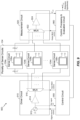
- the measurement and detection circuit 108 may include signal processing circuitry configured to process and filter the measurement output and determine whether an object 110 is potentially present (e.g., based on a time-differential detection approach). At least a portion of the measurement and detection circuit 108 may be implemented by one or more micro-controllers or processors. For example, at least a portion of the measurement and detection circuit 108 may be implemented as an application-specific integrated circuit (ASIC), a field programmable gate array (FPGA) device, digital signal processor (DSP), or another processor device. The measurement and detection circuit 108 may be configured to receive information from each of the components of the object detection circuit 108 and perform calculations based on the received information.
- ASIC application-specific integrated circuit
- FPGA field programmable gate array
- DSP digital signal processor
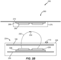
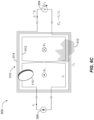
- the wireless power transfer structure 224 (also sometimes referred to as a "pad") is configured to wirelessly transmit or receive power.
- FIG. 2A illustrates one example of a wireless power transfer structure 224 and how the sense element array 106 of FIG. 1 may be integrated.
- the wireless power transfer structure 224 includes a coil 226 also referred to as the wireless power transfer coil that is configured to generate an alternating magnetic field when driven with a current by the power conversion circuit 222.
- the wireless power transfer structure 224 may further include ferrite 228 configured to channel and/or provide a path for magnetic flux ( e.g., may be arranged in one or more ferrite bars which can be a combination of ferrite tiles arranged to form the bars).
- the size of each sense element of the plurality of sense elements 106a, 106b, ..., 106n may be either on the order of this minimum size or a multiple thereof ( e.g., with a 10-times larger area), assuming that those minimum size objects are located in close proximity of a plane defined by the array 106 ( e.g., on the top surface of the housing 236 of the base pad as shown later in FIG. 2B ).
- the number N of sense elements of the array 106 could be on the order of 64 ( e.g., 8 ⁇ 8 array) to be able to provide coverage of the entire predetermined area with the required sensitivity.
- the system shown in FIG. 2A may include a housing (not shown in FIG. 2A but shown later in FIG. 2B as housing 236) configured to house, for example at least the wireless power transfer coil 226, the ferrite 228, the sense element array 106, and potentially the shield 230.
- the housing may be made of any suitable material (e.g., hard plastic, ceramics etc.) and can be designed to provide structural support for example to support the weight of various objects such as vehicles that may pass over the housing.
- the housing may be made of a non-conductive material to avoid interfering or interacting with the magnetic field 232.
- All or just a portion of the power conversion circuit 222 may also be housed in the housing 236. Although in some implementations the power conversion circuit 222 may be housed separately from the housing 236 that houses the wireless power transfer structure 224. In some cases, the power conversion circuit 222 is housed in the housing 236 but is positioned on the other side of the shield 230 from the ferrite 228.
- the shield 230 may form a portion of the housing 236.
- the power conversion circuit 222 is not shown but may be electrically connected to the wireless power transfer coil 226 or a portion or all may also be housed in the housing 236.
- the vehicle-side wireless power receive structure 260 includes a wireless power transfer coil 266, a layer of ferrite 268, and a shield 270 made of an electrically conductive material.
- the shield 270 may be formed from a portion of the apparatus that the ferrite 268 and the wireless power transfer coil 266 are affixed to ( e.g., the metallic underbody of a vehicle).
- a housing 276 configured to house the wireless power transfer coil 266 and ferrite 268 is provided but that would not house the shield 270.
- a shield 270 e.g., a back plate
- a power conversion circuit 222 is not shown but may be electrically connected to the receive coil 268 or a portion or all may also be housed in the housing 276.
- FIGs. 3 to 8 illustrate examples of different techniques based on measuring at least one electrical characteristic that may be used in conjunction with the object detection circuit 100 of FIG. 1 .
- These examples are to illustrate the principle of the sensing and measurement technique and do not show all the details of an object detection circuit 100. Particularly, they do not show the further signal processing and evaluation circuit as it may be required e.g., for detecting an object based on a change in a measured electrical characteristic.
- these techniques are illustrated by means of a single sense element though applicable to a plurality of sense elements (e.g., sense elements 106a, 106b, ..., 106n) as described below with reference to FIGs. 10 to 14 .
- FIG. 3A shows a circuit 300 to illustrate a technique for inductively sensing a presence of an object 110 based on a change in a complex impedance Z 1 as measured at the terminals of sense coil 302 (e.g., a planar a multi-turn coil) with inductance L 1 that may represent e.g., sense element 106a.
- sense coil 302 e.g., a planar a multi-turn coil
- L 1 may represent e.g., sense element 106a.
- a change ⁇ Z 1 of the impedance Z 1 relative to the impedance Z 1,0 in the absence of the object 110 may indicate a presence of the object 110.
- a change of impedance may be also produced when the sense coil 302 is integrated into the wireless power transfer structure 224 as shown in FIG.
- the circuit 300 of FIG. 3A illustrates a technique for measuring an impedance Z 1 where a sinusoidal current I 1 with a defined frequency, amplitude, and phase provided by a current source 306 is applied to the sense coil 302 and where the open-circuit voltage V 1 across the terminals of the sense coil 302 is measured.
- the open-circuit voltage V 1 is measured using a sensitive high impedance voltage measurement circuit 304 so that there is virtually zero current at the terminals of the voltage measurement circuit 304 ( I 2 ⁇ 0).
- This impedance measurement technique is also referred herein as to the current source voltage measurement approach.
- the current source 306 and the voltage measurement circuit 304 may be part of the measurement and detection circuit 108 with reference to FIG. 1 .
- the voltage measurement circuit 304 may be frequency selective (narrowband) tuned to the sense frequency f s (frequency of the current source) which may be e.g., in the MHz range.
- a change ⁇ Z 1 in the impedance Z 1 e.g., due to presence of the object 110 manifests in a change ⁇ V 1 in the voltage V 1 while the current I 1 remains unaffected. Therefore, measuring a change ⁇ V 1 in the voltage V 1 may be equivalent to measuring a change ⁇ Z 1 in the impedance Z 1 . In other words, the voltage V 1 may be indicative of the impedance Z 1 .
- impedance measurement techniques are also contemplated e.g., by applying a sinusoidal voltage source with a defined voltage V 1 (amplitude and phase) and measuring the current I 1,0 + ⁇ I 1 at the sense coil 302 using a sensitive ( e.g., frequency selective) low impedance current measurement circuit.
- This impedance measurement technique is also referred herein as to the voltage source current measurement approach.
- Equation (3) may apply to the current source (e.g., current source 306) as it may be used in implementations based on any of the impedance or mutual impedance sensing techniques described herein.
- the voltages V 1,0 and ⁇ V 1 in Equation (3) refer to the respective voltages across the output of the current source (e.g ., current source 306) and the currents I 1,0 and ⁇ I 1 to the respective currents at the output of the current source.
- the voltage source in an implementation of the voltage source current measurement approach may be characterized by a quasi-ideal voltage source.
- a quasi-ideal sinusoidal voltage source may be defined as a sinusoidal signal source with a sufficiently small (but non-zero) source impedance so that the magnitude of the fractional change of its output voltage
- Equation(5) may apply to the voltage measurement circuit (e.g., voltage measurement circuit 304) as it may be used in implementations based on any of the impedance and mutual impedance sensing techniques described herein.
- the voltages V 1 and V 1, ⁇ in Equation(5) refer to the respective voltages across the input of the voltage measurement circuit (e.g., voltage measurement circuit 304).
- FIG. 3B An equivalent circuit of the circuit 300 of FIG. 3A including a circuit model of the object 110 is shown in FIG. 3B .
- the sense coil 302 is represented by an equivalent inductance L 1 ( ⁇ ) and an equivalent loss resistance R 1 ( ⁇ ) both shown as a function of temperature ⁇ .
- inductance L 1 ( ⁇ ) may include a change of an inductance due to the presence of materials 310. Depending on the electromagnetic properties of materials 310, this may be a decrease or increase of the inductance L 1 ( ⁇ ) as measured in free space.
- the loss resistance R 1 ( ⁇ ) may include two resistance components.
- a first resistance component may be attributed to the resistance of the sense coil's conductive structure (e.g., copper wires or PCB traces) as experienced at the sense frequency f s (subject of skin and proximity effects).
- a second resistance component may be due to loss effects in materials 310 ( e.g., eddy current and/or hysteresis losses). It may be appreciated that both resistance components may be subject of thermal effects, e.g., they may increase if the temperature inside the housing 236 of the wireless power transfer structure 224 rises.
- the DC resistance of a sense coil's 302 copper winding may vary by 40% for a temperature variation over the range from -20°C to +80°C as it might be specified for an installation in an outdoor environment and assuming a temperature coefficient of 0.004 Q/K for copper and a linear relationship.
- This resistance variation may be smaller (in the order of 20%) at sense frequency f s ( e.g., in the MHz range), taking skin and proximity effects into account, since current distribution inside the sense coil's 302 conductive structure ( e.g., wire) also changes with the electrical conductivity and thus with temperature.
- a similar variation may be expected in the second resistance component if eddy current losses in the materials 310 are the predominant loss effect.
- / R 1 ( ⁇ ) produced by a small object 110 may be in the order of only 0.1% assuming a cost optimized implementation of the object detection circuit 100 of FIG. 1 providing a plurality of sense coils 106a, 106b, and 106 n each with a form factor in the order of 60 x 80 mm.
- This example demonstrates that significant changes in impedance Z over time may occur if the object detection circuit 100 is operated in an outdoor environment.
- object detection may require a differential detection approach (e.g., a time differential detection scheme) rather than detection on an absolute basis (absolute detection) e.g., by comparing the measured impedance Z 1 against a reference value Z 1,ref that has been determined in a process of calibration e.g., at time of installation or commissioning of the wireless power transfer structure 224 as further discussed below.
- a differential detection approach e.g., a time differential detection scheme
- absolute detection absolute basis
- the object 110 is modelled by an equivalent inductance L 3 and an equivalent loss resistance R 3 justified by the fact that an object 110 in general can store and dissipate electrical energy.
- An LR-model may apply to a metallic object 110 that appears electrically conductive but non-ferromagnetic at sense frequency f s . It may not apply to an object 110 that appears ferromagnetic or dielectric at sense frequency f s as further discussed below.
- An object 110 not exhibiting a noticeable ferromagnetic effect (e.g., a magnetic relative permeability ⁇ r > 1 ) at sense frequency f s may be referred to as a non-ferromagnetic object.
- an electrically conductive object 110 that appears ferromagnetic at sense frequency f s is referred to as a ferromagnetic conductive object 110.
- Modelling of a ferromagnetic conductive object 110 may be more complex than shown in FIG. 3B by an equivalent LR circuit model. Magnetic coupling between object 110 and sense coil 302 (between inductance L 3 and inductance L 1 ) is modelled by coupling factor k 13 . Practical experience with many different types of non-ferromagnetic objects 110 shows that variations of position and orientation of the object 110 relative to sense coil 302 mainly affect the coupling factor k 13 but generally have a minor impact on the parameters of its LR model.
- the transformation factor ⁇ 13 is also a scalar and the change in impedance ⁇ Z 1 reflects the conjugate complex of the impedance of the object 110 with respect to the Q-factor or the angle (argument) of the impedance Z 3 .
- a Q-factor may be attributed to the object 110 since the object 110 in general can store and dissipate energy. Eddy currents are induced into a metallic object 110 when subjected to the magnetic sense field as generated by sense coil 302. Energy is stored in the secondary magnetic field produced by the induced eddy currents in the object 110 (inductance L 3 ) and dissipated in its resistance R 3 .
- Equation (10) indicates that presence of a non-ferromagnetic metallic object 110 with finite electrical conductivity, which can be modelled with resistance R 3 > 0 and inductance L 3 > 0, produces a positive Re ⁇ Z 1 ⁇ and a negative Im ⁇ Z 1 ⁇ . Otherwise stated, it produces an increase of equivalent resistance and a decrease (destruction) of equivalent inductance in the circuit 300.
- FIG. 3D illustrates a complex plane 330 or more precisely a complex half plane comprising quadrant 1 and 4 where the impedance changes ⁇ Z 1 (responses) of different types (categories) of objects 110 may occur. More particular, FIG. 3D shows shaded areas (angle ranges) corresponding to different categories of objects 110 where ⁇ Z 1 may be measured at a sense frequency f s ( e.g., in the MHz range) if the object 110 is placed in proximity of the sense coil 302. To emphasize the characteristics of the different categories of objects 110, the angle ranges indicated in FIG. 3D may be not drawn to scale and should be considered qualitative rather than quantitative. The actual angle ranges may also depend on the particular sense frequency f s . Since the Q-factor of some categories of object 110 generally increases with frequency, some areas will move closer to the imaginary axis when the sense frequency f s is increased.
- a non-ferromagnetic object 110 with a well conducting surface may produce a ⁇ Z 1 in the angle range 331 close to the negative imaginary axis in the 4 th quadrant of the complex plane 330 indicating an object 110 with a relatively high Q-factor Q 3 .
- the angle range 332 that is also in the 4 th quadrant may be characteristic for a piece of thin foil or a metallized (aluminum coated) paper.
- the angle range 333 may be typical for the response ⁇ Z 1 of some ferromagnetic steel objects (e.g., nuts). These objects 110 are electrically conductive but also exhibit a relative permeability ⁇ r > 1. The effect of ferromagnetism in these objects 110 may be threefold. First, it may increase the reactance Im ⁇ Z 1 ⁇ of the sense coil 302. Second, it may increase the loss resistance Re ⁇ Z 1 ⁇ compared to an equal but non-ferromagnetic object with the same conductivity ⁇ since skin depth ⁇ reduces thus resistance R 3 increases with increasing permeability ⁇ r as evident from equation (15). Third, since the object 110 is conductive, it may also destroy reactance of the sense coil 302 at the same time.
- the net response produced by some ferromagnetic steel objects 110 may be found close to the real axis in the angle range 333 (e.g., Im ⁇ Z 1 ⁇ ⁇ 0) in the 4 th or in the 1 st quadrant of the complex plane 330.
- some ferromagnetic steel objects 110 e.g., nuts
- the real axis in the angle range 333 e.g., Im ⁇ Z 1 ⁇ ⁇ 0
- such objects 110 may appear as stealth objects 110.
- Ferromagnetic steel objects 110 with a cylindrical shape of diameter d much smaller than its length l may produce a response ⁇ Z 1 in the angle range 334 around 45° in the 1 st quadrant somewhat depending on its orientation relative to the magnetic sense field.
- the ferromagnetic effect increasing a reactance Im ⁇ Z 1 ⁇ may be much larger than the reactance destroying effect of its conductivity.
- These objects 110 may produce an impedance change ⁇ Z 1 with a positive Q-factor Q ⁇ Z 1 close to unity.
- Ferromagnetic non-conductive objects 110 with low resistive losses may produce a response ⁇ Z 1 in the angle range 335 close to the positive imaginary axis corresponding to a high positive Q-factor Q ⁇ Z 1 .
- a similar response ⁇ Z 1 in the angle range 335 may be also produced by dielectric non-conductive objects 110 with low resistive losses (e.g., a human hand, a plastic bottle filled with water).
- Dielectric objects 110 may interact with the sense coil 302 via the electric field generated by the sense coil's 302 self-capacitance that may be modelled by a capacitance C 1, self in parallel to the equivalent circuit of the sense coil 302 (not shown in FIG. 3B but considered merged into the equivalent inductance L 1 ).
- a dielectric non-conductive object 110 with low resistive losses in proximity of the sense coil 302 may generally increase self-capacitance C 1, self resulting in an increase of reactance (Im ⁇ Z 1 ⁇ > 0) as evident from the following equation: L 1 ⁇ L 1 , ex + ⁇ s 2 L 1 , ex 2 C 1 , self , where L 1, ex denotes the sense coil's 302 inductance excluding self-capacitance.
- the sense coil 302 may be used for capacitive sensing of living objects e.g., a human hand, a cat, or any other animal that are predominantly dielectric and that may be located in proximity of sense coil 302. Such use case may require the object detection circuit 100 to discriminate dielectric objects from metallic objects e.g., if rules and procedures for living object detection would differ from those applied to metal object detection.
- the highest loss power density e.g., Watt per unit surface area
- the object detection circuit 100 may be configured to measure an impedance change ⁇ Z 1 with sufficient accuracy at least with respect to its angle arg ⁇ Z 1 ⁇ . Even higher accuracy (e.g., angle fidelity) may be required if an object detection circuit 100 employs a time-differential detection scheme as further described in connection with FIG. 9 .
- a fast (e.g ., abrupt) change ⁇ Z 1 in a sequence (time-series) of consecutively measured impedances Z 1 due to the object 110 brought to proximity of sense coil 302 may cause a time-differential detector to temporarily produce an output indicative for ⁇ Z 1 .
- a fast (e.g., abrupt) change ⁇ Z 1 due to the object 110 removed from the proximity of sense coil 302 may cause the time-differential detector to temporarily produce an output indicative for - ⁇ Z 1 (opposite sign). Therefore, outputs of a time-differential detector may fall in all four quadrants of the complex plane 330, depending on the characteristics ( e.g., impedance) of the object 110 and whether it is brought to or removed from the proximity of the sense coil 302.
- the object detection circuit 100 of FIG. 1 may be configured to provide accurate calibration of the impedance measurement at least with respect to its angle arg ⁇ Z 1 ⁇ . This may be particularly true for implementations of the object detection circuit 100 of FIG. 1 relying on an impedance measurement circuit (e.g., including a quasi-ideal current source 306 and a quasi-ideal voltage measurement circuit 304) that is subjected to measurement errors.
- an impedance measurement circuit e.g., including a quasi-ideal current source 306 and a quasi-ideal voltage measurement circuit 304
- the object detection sensitivity may be defined as the impedance change ⁇ Z 1 as produced in presence of an object 110 normalized to
- This normalized impedance change (sensitivity) is herein also referred to as the fractional change ⁇ Z 1 /
- equation (19) may be expressed solely in terms of coupling factor k 13 and the object's 110 Q-factor Q 3 as follows: ⁇ Z 1 Z 1 , 0 ⁇ k 13 2 Q 3 1 + Q 3 2 1 ⁇ j Q 3 ,
- equation (20) may be rewritten as ⁇ Z 1 Z 1 , 0 ⁇ k 13 2 1 Q 3 ⁇ j Equation (21) shows that the imaginary part of the fractional change ⁇ Z 1 /
- may determine the required dynamic range of the voltage measurement circuit 304. It may be appreciated that detection of objects 110 with a low fractional change
- may also at least partially determine temperature sensitivity of the object detection circuit 100 as a consequence of a temperature dependent impedance Z 1,0 as previously discussed in connection with FIG. 3B .
- Temperature sensitivity may be defined e.g., with respect to the real part as the ratio of an impedance change Re ⁇ ⁇ Z 1,0 ⁇ due to a temperature change ⁇ ⁇ to an impedance change Re ⁇ Z 1 ⁇ produced by the object 110.
- This ratio e.g., with respect to the real part may be also expressed as the ratio of the fractional changes Re ⁇ ⁇ Z 1,0 ⁇ /
- Equation (22) shows that temperature sensitivity with respect to the real part may reduce if the fractional change Re ⁇ Z 1 ⁇ /
- may be increased by reducing the size of the sense coil 302.
- a smaller sense coil size may be used which may result in a larger number of sense coils.
- a sense coil 302 may be implemented with a spread (spiral) winding (as opposed to a more concentrated winding as illustrated in FIG: 3A ) which may provide a larger fractional change
- SNR signal-to-noise ratio
- V 1,n denotes an equivalent r.m.s. noise voltage at sense frequency f s in the bandwidth B m of the voltage measurement circuit 304.
- An equivalent noise voltage source V 1,n (not shown in FIG. 3C ) may be considered in series to the impedance Z 1 in the equivalent circuit of FIG. 3C .
- This equivalent noise voltage source may generally include the effect of various circuit intrinsic and extrinsic noise sources.
- Circuit intrinsic noise may include thermal noise generated by the resistance R 1 and in the voltage measurement circuit 304.
- Noise produced in the voltage measurement circuit 304 may include thermal noise and quantization noise e.g., if the voltage measurement circuit 304 involves an analog-to-digital converter (ADC).
- the circuit intrinsic noise may also include noise generated in the current source 306 e.g., a noise current component producing a noise voltage across impedance Z 1 .
- this noise current may include additive noise, phase noise and amplitude modulated (AM) noise.
- Additive noise may include thermal noise as generated in the circuit of the current source 306. It may also include quantization noise if the current source involves a digital signal synthesizes and a digital-to-analog converter (DAC).
- DAC digital-to-analog converter
- the effect of DAC quantization noise may appear as a deterministic error on the current amplitude rather than a stochastic noise component.
- the amplitude of current I 1 may be modulated by a low frequency noise component with a 1/ f -characteristics, e.g., if the current source 306 involves a DC supply voltage regulator that generates low frequency noise. Therefore, some implementations of the object detection circuit 100 of FIG. 1 use a current source 306 and a voltage measurement circuit 304 optimized with respect to all sort of noise components to maximize a sensitivity (e.g., the SNR as defined by Equation (24)) with respect to circuit intrinsic noise.
- a sensitivity e.g., the SNR as defined by Equation (24)
- Switching noise in the wireless power electromagnetic field produced by the power conversion circuit 222 may be inductively and/or capacitively coupled into sense coil 302 when the wireless power transfer system is active.
- This circuit extrinsic noise component may include wideband and narrowband noise (e.g., harmonics noise). Therefore, in some implementations of a wireless power transfer system 200 including an object detection circuit 100, the power conversion circuit 222 is optimized with respect to noise e.g., by using extra filtering to suppress noise in a sense frequency band.
- the voltage measurement circuit 304 may be configured to minimize the effect of circuit extrinsic noise sources.
- the noise spectrum is monitored with a spectral resolution corresponding to the bandwidth B m of the voltage measurement circuit 304 to identify potential sense frequencies f s with lowest noise level and within some operational frequency limits determined by the object detection circuit 100.
- the object detection circuit 100 may select a sense frequency f s at a frequency providing lowest noise level. Such procedure may be used to maximize the SNR as defined by Equation (24)) with respect to circuit extrinsic noise and thus to maximize sensitivity of the object detection circuit 100 e.g., in presence of switching noise.
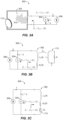
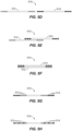
- FIG. 4A shows a circuit 400 illustrating another technique for inductively detecting a presence of an object 110.
- Circuit 400 uses a capacitor 420 having capacitance C to compensate for the reactance ⁇ s L 1 of the sense coil 302 having an inductance L 1 .
- capacitor 420 may not fully compensate for the sense coil's 302 reactance at a specified sense frequency f s ( e.g., in the MHz range).
- the frequency of the current source defining the sense frequency f s may be adjustable so that the LC-circuit may be tuned for improved compensation (resonance) in the absence of an object 110.
- FIG. 4B An equivalent circuit of the circuit 400 of FIG. 4A is illustrated in FIG. 4B .
- the sense coil 302 is represented by an equivalent inductance L 1 ( ⁇ ) and an equivalent loss resistance R 1 ( ⁇ ), and the compensation capacitor 420 by its equivalent capacitance C ( ⁇ ), all three shown as a function of temperature ⁇ .
- inductance L 1 ( ⁇ ) and resistance R 1 ( ⁇ ) may include a change of an inductance and resistance, respectively, due to the presence of materials 310. Depending on the electromagnetic properties of materials 310, this may be a decrease or increase of the inductance L 1 ( ⁇ ) and resistance R 1 ( ⁇ ) as measured in free space.
- the object 110 is abstracted away by impedance change ⁇ Z 1 as previously discussed.
- the impedance Z 1c,0 as measured in absence of object 110 may only include the equivalent resistance R 1 ( ⁇ ).
- equation (26) may be rewritten as ⁇ Z 1 Z 1 c , 0 ⁇ k 13 2 Q 1 1 Q 3 ⁇ j .
- reactance compensation as illustrated by circuit 400 of FIG. 4A may increase sensitivity for various objects.
- impedance measurement may be subjected to measurement errors.
- Reactance compensation may provide a mean for accurate calibration of the impedance measurement e.g., with respect to the angle arg ⁇ Z 12 c ⁇ for purposes as previously discussed in connection with the circuit 300 of FIG. 3A .
- the frequency f s of the current source 306 is tuned such that the magnitude impedance
- the object detection circuit 100 may correct as part of a calibration procedure the actually measured impedance measurement by rotating the impedance plane so that the Im ⁇ Z 1 c ,0 ⁇ vanishes.
- reactance compensation may also allow a sense current I 1 to be increased by a factor of Q 1 , which may in turn result in an increase of the signal-to-noise ratio (SNR) with respect to external noise (e.g., high frequency noise and harmonics in the electromagnetic fields as generated for the wireless power transfer) that is coupled into the sense coil 302.
- SNR signal-to-noise ratio
- reactance compensation using a series capacitor 420 together with a voltage measurement circuit 304 that presents a high input impedance at sense frequency f s and a low impedance at low frequencies may form a high pass filter to attenuate low frequency signal components e.g., at the wireless power transfer frequency f wpt ( e.g., 85 kHz) as described in more detail in connection with FIG. 10 .
- f wpt e.g. 85 kHz
- reactance compensation may not reduce a temperature sensitivity of the object detection circuit 100 as it may be defined in analogy to equations (22) and (23) respectively, since reactance compensation may not reduce a change ⁇ Z 1 c ,0 due to a change in temperature ⁇ ⁇ .
- the change of Im ⁇ ⁇ Z 1 c ,0 ⁇ may be generally larger than Im ⁇ ⁇ Z 1,0 ⁇ if compensation capacitor 420 is also a function of temperature ⁇ .
- temperature sensitivity is reduced by either using a capacitor with a low temperature coefficient (e.g., NP0-type) or with a temperature coefficient that compensates or partially compensates for the temperature drift of the sense coil's impedance Z 1,0 .
- a capacitor with a low temperature coefficient e.g., NP0-type
- a temperature coefficient that compensates or partially compensates for the temperature drift of the sense coil's impedance Z 1,0 e.g., NP0-type
- circuits 300 and 400 of FIGs. 3A and 4A illustrate a technique for detecting an object 110 based on measuring a self-impedance Z 1 or a capacitively compensated self-impedance Z 1 c of a sense coil 302, respectively
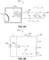
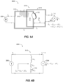
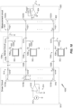
- the circuit 500 of FIG. 5A illustrates another technique for detecting an object 110 based on measuring a transimpedance Z 12 between a first (primary) sense coil 512 with inductance L 1 and a second (secondary) sense coil 514 with inductance L 2 of a sense coil arrangement 510.
- a change ⁇ Z 12 of the transimpedance Z 12 relative to the transimpedance Z 12,0 in the absence of the object 110 may indicate a presence of the object 110 in proximity of at least one of the two sense coils 512 and 514.
- primary sense coil 512 and secondary sense coil 514 of the sense coil arrangement 510 are planar multi-turn coils and are disposed such that there is magnetic coupling between the two sense coils (e.g., sense coils may be overlapping as shown in FIG. 5A ).
- a change of transimpedance ⁇ Z 12 may be also experienced when the two sense coils 512 and 514 are integrated together with the wireless power transfer structure 224 into housing 236 as shown in FIG. 2A due to presence of materials 310 as previously discussed. Presence of materials 310 is indicated in FIG. 5A by the shaded area.
- Materials 310 may also include a dielectric substrate that carries the two sense coils 512 and 516 or a dielectric medium the sense coils are embedded in ( e.g., in case of a printed circuit board (PCB) design).
- the effects of materials 310 may generally produce a change in the sense coils' 512 and 514 self-impedance Z 1,0 and Z 2,0 , respectively, and in the transimpedance Z 12,0 relative to these impedances as measured in free space.
- the effects of materials 310 are considered already included in Z 1,0 , Z 2,0 and Z 12,0 .
- the circuit 500 of FIG. 5A illustrates a technique for measuring a transimpedance Z 12 based on the current source voltage measurement approach.
- a sinusoidal current I 1 with a defined frequency, amplitude, and phase provided by a current source 306 is applied to the primary sense coil 512 and the open-circuit voltage V 2 is measured across the terminals of the secondary sense coil 514.
- the open-circuit voltage V 1 is measured using a sensitive high impedance voltage measurement circuit 304 so that there is virtually zero current at the terminals of the secondary sense coil 514 ( I 2 ⁇ 0).
- the current source 306 and the voltage measurement circuit 304 may be part of the measurement and detection circuit 108 with reference to FIG. 1 .
- the voltage measurement circuit 304 may be frequency selective (narrowband) tuned to the sense frequency f s (frequency of the current source) as previously discussed in connection with the circuit 300 of FIG. 3A .
- measuring a change ⁇ V 2 in the voltage V 2 may be equivalent to measuring a change ⁇ Z 12 in the transimpedance Z 12 .
- the voltage V 2 may be indicative of the transimpedance Z 12 .
- the current source 306 and the voltage measurement circuit 304 used in an implementation of the circuit 500 of FIG. 5A may be characterized by a quasi-ideal current source and a quasi-ideal voltage measurement circuit, respectively, as defined in connection with the circuit 300 of FIG. 3A .
- the transimpedance as measured between a pair of sense coils depends on the measurement technique (e.g., on loading conditions of sense coils 512 and 514).
- the transimpedance as measured with the current source voltage measurement approach illustrated by the circuit 500 of FIG. 5A may be also referred to as the mutual impedance.
- FIG. 5B An equivalent circuit of the circuit 500 of FIG. 5A including a circuit model of the object 110 is shown in FIG. 5B .
- the primary sense coil 512 and secondary sense coil 514 are each represented by an equivalent inductance L 1 ( ⁇ ) and L 2 ( ⁇ ), respectively, and by an equivalent loss resistance R 1 ( ⁇ ) and R 2 ( ⁇ ), all shown as a function of temperature ⁇ .
- the equivalent loss resistances R 1 ( ⁇ ) and R 2 ( ⁇ ) may each include a first resistance component due to losses in the sense coil's conductive structure ( e.g., copper wires or PCB traces) and a second resistance component due to loss effects in materials 310 as previously discussed in connection with FIG. 3B .
- Magnetic coupling between sense coils 512 and 514 is represented by a complex coupling factor k 12 ( ⁇ ), also shown as a function of temperature ⁇ as further explained below.
- the equivalent inductances and resistance L 1 ( ⁇ ), L 2 ( ⁇ ), R 1 ( ⁇ ) and R 2 ( ⁇ ), respectively, as well as the coupling factor k 12 ( ⁇ ) may include a change due to the presence of materials 310. Since the electromagnetic properties of materials 310 may generally be temperature dependent, some temperature dependence may be expected for the coupling factor k 12 ( ⁇ ).
- the change in k 12 ( ⁇ ) due to materials 310 may include a real and imaginary component due to reactive and resistive (loss) effects, respectively, in materials 310 but also due to mutual loss effects e.g., an eddy current loss effect in the secondary sense coil 514 produced by the magnetic field of the primary sense coil 512.
- FIG. 5B shows each of the primary sense coil 512 and the secondary sense coil 514 magnetically coupled with coupling factor k 13 and k 23 , respectively, to the object 110 represented by an LR-Model ( L 3 , R 3 ) as previously discussed e.g. , with reference to FIG. 3B .
- the effect of presence of the object 110 in proximity of coil arrangement 510 may be threefold. First, it produces a change ⁇ Z 1 in the impedance Z 1 as it would be measured at the terminals of sense coil 512. Second, it produces a change ⁇ Z 2 in the impedance Z 2 as it would be measured at the terminals of sense coil 514.
- FIG. 5C shows an equivalent circuit of the circuit 500 of FIG. 5A .
- Each of the three branch impedances is composed of an inductance, resistance and an impedance change due to presence of the object 110. More precisely, the equivalent circuit of FIG. 5B shows the model of the object 110 abstracted away by impedance change ⁇ Z 1 - ⁇ Z 12 and ⁇ Z 2 - ⁇ Z 12 in the first and second series branch impedance Z 1 - Z 12 and Z 2 - Z 12 , respectively, and by a change of mutual impedance ⁇ Z 12 in the shunt branch impedance Z 12 . Though not shown in FIG. 5C for illustrative purposes and simplicity, each of the equivalent circuit elements may be temperature dependent.
- leakage inductances L 1 - M 12 and L 2 - M 12 , equivalent series resistances R 1 - R 12 and R 2 - R 12 , and impedance changes ⁇ Z 1 - ⁇ Z 12 and ⁇ Z 2 - ⁇ Z 12 have ideally no effect in the transimpedance measurement.
- the sensitivity of the object detection circuit 100 of FIG. 1 based on the mutual impedance sensing technique may be defined as the mutual impedance change ⁇ Z 12 as produced in presence of an object 110 normalized to
- This normalized mutual impedance change (sensitivity) may be also referred to as the fractional change ⁇ Z 12 /
- Equation (52) For a sense coil arrangement 510 with high enough mutual inductance ⁇ s M 12 ⁇ R 1 , the magnitude mutual impedance
- equation (54) may be expressed analogously to equation (20) solely in terms of coupling factors k 13 , k 23 , k 12 and the object's 110 Q-factor Q 3 as follows: ⁇ Z 12 Z 12 , 0 ⁇ k 13 k 23 k _ 12 Q 3 1 + Q 3 2 1 ⁇ j Q 3 ,
- equation (55) may be rewritten as ⁇ Z 12 Z 12 , 0 ⁇ k 13 k 23 k _ 12 1 Q 3 ⁇ j
- ⁇ 1 e.g., using two identical sense coils on top of each other and with zero displacement as shown by FIG.
- Equation (57) indicates that the mutual impedance sensing technique has the potential to provide a sensitivity (fractional change) equal to that of self-impedance sensing (Equation (21)) assuming equal coupling to the object 110 for both sensing methods (circuit 300 of FIG. 3A and circuit 500 of FIG. 5A ).
- SNR I 1 2 ⁇ ⁇ Z 1 2 V 1 , n 2 ⁇ I 1 2 ⁇ ⁇ Z 12 2 V 2 , n 2 .
- k 13 ⁇ k 23 e.g., primary and secondary sense coil are physically displaced e.g., as illustrated by FIG. 5D
- a lower SNR may be expected from mutual impedance sensing (circuit 500).
- This feature may allow the object detection circuit 100 to discriminate certain categories of objects and/or increase a sensitivity for certain categories of objects as previously discussed in connection with the self-impedance sensing technique (circuit 300) as illustrated by FIG. 3A .
- transimpedance measurement techniques may be used e.g., the voltage source current measurement approach as previously described in connection with the circuit 300 of FIG. 3A .
- the expression in brackets generally is a non-scalar (complex) transformation factor. Therefore, the change ⁇ Z 12 in transimpedance may be no more proportional to the object's 110 sign-inverted impedance - Z 3 , hence arg ⁇ Z 12 ⁇ ⁇ - arg ⁇ Z 3 ⁇ ). Moreover, the resulting angle arg ⁇ Z 12 ⁇ may vary with position and orientation of the object 110 relative to the sense coil arrangement 510. In some aspects of transimpedance sensing, this finding may be considered as a difficulty of the voltage source current measurement approach.
- the object detection circuit 100 is configured to calibrate the mutual impedance measurements for purposes as previously described in connection with FIGs. 3A to 3D .
- implementation of the calibration may result in higher circuit complexity and cost in certain aspects, e.g., if compared to aspects of capacitively compensated self-impedance sensing using sense frequency tuning as discussed in connection with FIG. 4A .
- FIGs. 5D to 5H are cut views illustrating various exemplary implementations of planar sense coil arrangements 510 as they may be used for transimpedance (e.g., mutual impedance) sensing.
- FIG. 5D illustrates an implementation of a sense coil arrangement 510 where sense coils 512 and 514 are coplanar and adjacent.
- This sense coil arrangement 510 may apply to an implementation using a plurality of substantially equal sense elements 106a, 106b, ... , 106n each including a single planar sense coil arranged in an array 106 with reference to FIG. 2A . Pairs of neighboring sense coils (e.g., sense coil 106a and 106b) may be temporarily configured using a multiplexer circuitry as further discussed with reference to FIG. 10 .
- a first pair may be configured by sense coils 106a and 106b, a second pair may be configured by sense coils 106b and 106c, a third pair may be configured by sense coils 106c and 106d etc.
- Sense coils pairs that are temporarily ( e.g., sequentially) configured may be overlapping. It may be also appreciated that in such implementation or operation, the number of double sense coil arrangements 510 that can be potentially configured is larger than the number N of sense elements of the array 106.
- FIG. 5E illustrates another implementation of a sense coil arrangement 510 where sense coils 512 and 514 are partially overlapping.
- This sense coil arrangement 510 may apply to an implementation using a plurality of substantially equal sense elements 106a, 106b, ..., 106n each including a single planar sense coil arranged in an array 106 having a first and second plane.
- Sense coils in the first plane are offset relative to the sense coils in the second plane by half of the width of the sense coil.
- Pairs of overlapping sense coils e.g., with a primary sense coil 512 in a first plane and a secondary sense coil 514 in a second plane may be temporally ( e.g., sequentially) configured using a multiplexer circuitry as further discussed with reference to FIG.
- a first pair may be configured by sense coil 106a in the first plane and sense coil 106b in the second plane
- a second pair may be configured by sense coil 106b in the second plane and sense coil 106c in the first plane
- a third pair may be configured by sense coils 106c in the first plane and sense coil 106d in the second plane, etc.
- Sense coil pairs temporarily configured in this way may be overlapping.
- FIG. 5F illustrates a further implementation of a sense coil arrangement 510 where sense coils 512 and 514 are fully overlapping (on top of each other).
- This sense coil arrangement 510 may apply to an implementation using a plurality of sense elements 106a, 106b, ..., 106n arranged in an array 106.
- Each of the plurality sense elements 106a, 106b, ... , 106n includes a pair of planar sense coils stacked on top of each other.
- This sense coil arrangement 510 may be also considered as a bifilar winding structure with a first winding disposed in a first plane and a second winding disposed in a second plane.
- FIG. 5G illustrates yet another exemplary implementation of a sense coil arrangement 510 where sense coils 512 and 514 are coplanar and arranged inside of each other.
- This sense coil arrangement 510 may apply to an implementation using a plurality of sense elements 106a, 106b, ..., 106n arranged in an array 106.
- Each sense element includes a pair of coplanar sense coils arranged inside each other.
- FIG. 5H illustrates yet a further implementation of a sense coil arrangement 510 where sense coils 512 and 514 are coplanar and interleaved.
- This sense coil arrangement 510 may apply to an implementation using a plurality of sense elements 106a, 106b, ..., 106n arranged in an array 106 with reference to FIG. 2A .
- Each sense element includes a pair of interleaved coplanar sense coils.
- This sense coil arrangement 510 may be also considered as a bifilar winding structure with a first and a second winding in the same plane.
- FIG. 6A shows a circuit 600 to illustrate another technique based on the mutual impedance sensing approach as previously described with reference to FIGs. 5A to 5H .
- FIG. 6A shows the sense coil 514 displaced relative to the sense coil 512 by an amount D.
- FIG. 6A also indicates a first magnetic flux ⁇ 1 through the overlap area and a second flux ⁇ 2 in the opposite direction through the non-overlap area of sense coil 514.
- There may be a displacement D where the net magnetic flux ⁇ ⁇ ⁇ 1 - ⁇ 2 generated by the primary sense coil 512 and passing through the secondary sense coil 514 is virtually zero (flux balance) resulting in virtually zero coupling (
- perfect flux balance zero coupling
- Losses in materials 310 may cause a small out-of-phase component in the flux ⁇ 2 relative to flux ⁇ 1 so that the net flux ⁇ ⁇ may never vanish entirely for any displacement D within some limits.
- the displacement D between the primary sense coil 512 and secondary sense coil 514 may be adjusted to reduce coupling.
- the level of coupling may be negligible or at least reduced to below a threshold.
- the displacement D may be adjusted by design for minimum magnitude coupling
- a mutual impedance sensing technique operating at or near flux balance may be referred to as flux balanced mutual impedance sensing.
- flux balanced mutual impedance sensing is used to increase a sensitivity (fractional change ⁇ Z 12 /
- a sensitivity fractional change ⁇ Z 12 /
- the sensitivity gain in this example may be quantified approximately by 1/
- FIG. 6B shows a simplified equivalent circuit of the circuit 600 of FIG. 6A .
- the sense coil arrangement 512 is represented by a simplified 'T' equivalent circuit model neglecting first and second series branch impedance as previously described with reference to FIG. 5C .
- This simplification may be permissible for the current source voltage measurement approach, since first and second series branch impedance have virtually no impact in the mutual impedance measurement.
- This simplified equivalent circuit solely comprises the shunt branch impedance Z 12 including the residual mutual inductance M 12 , a residual resistance R 12 , and mutual impedance change ⁇ Z 12 that represents the object 110 abstracted away.
- Flux balanced impedance sensing may be also implemented using a special sense coil arrangement 510 as illustrated by circuit 600 in FIG. 6C .
- FIG. 6C shows the primary sense coil 512 as a "figure eight" or "DD"-type coil while the secondary sense coil 514 is shown as a "circular"-type coil. It may be appreciated that there exist other implementations or combinations providing flux balance in the secondary sense coil 514.
- the primary sense coil 512 is a "circular"-type coil and the secondary 514 is a "DD"-type coil.
- the sense element array 106 is integrated together with the wireless power transfer structure 224 into housing 236 as illustrated by FIG. 2B .
- the design of the sense elements of the plurality of sense elements 106a, 106b, ..., 106n may require some modifications to substantially compensate for the flux unbalancing effects of materials 310 as previously defined in connection with FIG. 3A . These design modifications may be individual for each sense element of the plurality of sense elements 106a, 106b, ..., 106n.
- min may not be achieved in each of the plurality of sense elements e.g., because the integration impact is difficult to predict or may vary over time due to mechanical changes, ageing, temperature variations, etc. resulting in some loss of sensitivity. Therefore, adjusting flux balance in situ may be desirable.
- the sense coil arrangement 510 used for flux balanced mutual impedance sensing, there may exist positions of the object 110 where flux remains virtually balanced even for an object 110 in close proximity to the sense coil arrangement 510, meaning reduced or virtually zero sensitivity ( ⁇ Z 12 ⁇ 0).
- the blind spot (sum of all positions where sensitivity is below a threshold) may be extremely narrow. Therefore, the likelihood that an object 110 comes to a rest in a blind spot may be very low.
- These positions may also somewhat dependent on type, size, and orientation of the object 110.
- the blind spot e.g., for a coin may be found in a narrow area along its vertical symmetry axis (not shown in FIG.
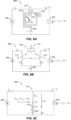
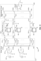
- FIG. 7A shows a circuit 700 illustrating a further technique which may be also referred to as flux balanced mutual impedance sensing.
- the circuit 700 is also based on the current source voltage measurement approach. It includes a sense coil arrangement 710 of two primary sense coils 512 with inductance L 1 and 516 with inductance L 3 and a secondary sense coil 514 with inductance L 2 .
- Each of the primary sense coils 512 and 516 is driven by a first and second current source 306 and 308 delivering currents I 1 and I 2 , respectively, e.g., with a sinusoidal current in the MHz range.
- the secondary sense coil 514 is electrically connected to the voltage measurement circuit 504 for measuring the open-circuit output voltage V 3 .
- the second current source 308 delivering current I 2 is controllable in amplitude and phase so that the circuit 700 may be operated such that the magnetic flux components as generated by sense coil 512 and 516 and passing through the secondary sense coil 514 cancel out (substantially zero flux or at least very low flux) resulting in substantially zero output voltage ( V 3 ⁇ 0) in absence of the object 110.
- FIG. 7 also shows an object 110 at an exemplary position in proximity of the sense coil arrangement 710. Since the output voltage V 3 is a function of two primary currents I 1 and I 2 , the definition of a transimpedance (e.g., Equation (28)) may generally not apply. Therefore, this technique may rely on measuring the output voltage V 3 and the object 110 is detected based on a change ⁇ V 3 in the output voltage V 3 relative to the voltage V 3,0 as measured in absence of the object 110.
- FIG. 7B shows an equivalent circuit of the circuit 700 including equivalent loss resistances R 1 , R 2 , and R 3 of sense coils 512, 516, and 514, respectively.
- Coupling between the first primary sense coil 512 and secondary sense coil 514 and between the second primary sense coil 516 and secondary sense coil 514 is represented by complex coupling factors k 13 and k 23 , respectively, as previously discussed in connection with FIG. 3B .
- Coupling between the two primary sense coils 512 and 516 may also exist but is omitted in FIG. 7B as it generally does not matter for the current source voltage measurement approach.
- It also includes an equivalent circuit model of the object 110 ( L 4 , R 4 ) and corresponding coupling to each sense coil (512, 514, and 516) represented by coupling factors k 14 , k 34 , and k 24 , respectively.
- FIG. 7C shows a simplified equivalent circuit of the circuit 700 to illustrate the voltage cancellation effect in output voltage V 3 .
- This equivalent circuit includes a simplified 'T'-equivalent circuit (transformer) models reduced to the shunt branch (mutual) impedances Z 13 and Z 23 , respectively, for each of the two transmission paths I 1 to V 3 and I 2 to V 3 .
- Each shunt branch impedance Z 13 and Z 23 incudes a mutual inductance M 13 and M 23 , an equivalent loss resistance R 12 and R 23 corresponding to the imaginary part of coupling factor k 13 and k 23 , respectively.
- Each of the shunt branch impedances Z 13 and Z 23 also includes a mutual impedance change ⁇ Z 13 and ⁇ Z 23 representing the model of the object 110 abstracted away.
- FIG. 7C also indicates the two primary currents I 1 and I 2 and the resulting partial voltages V 13 and V 23 across shunt branch impedance Z 13 and Z 23 , respectively.
- the second current source 308 can be precisely adjusted to the required value in terms of both amplitude and phase, perfect voltage cancellation may be achieved.
- Phase adjustment may be needed if materials 310 unequally affect the coupling factors k 13 and k 23 in terms of the loss angle so that arg ⁇ k 13 ⁇ ⁇ arg ⁇ k 23 ⁇ results.
- ⁇ V 3 ⁇ V 13 + ⁇ V 23 ⁇ 0 in presence of the object 110.
- the blind spot may be found along a diagonal line of sense coil 514 corresponding with the symmetry line (not shown in FIG. 7a ) of the sense coil arrangement 710.
- the sense coil arrangement 710 of FIG. 7A may provide sensitivity above the entire area spanned by the three sense coils 512, 514, and 516 and even outside this area to some extent.
- the circuit 700 may provide an infinite sensitivity with respect to the fractional change ⁇ V 3 /
- the circuit 700 potentially allows for angle-true impedance measurement for purposes as previously discussed in connection with FIG. 3D , if the phase angle of the currents I 1 and I 2 are similar (arg ⁇ I 1 ⁇ ⁇ arg ⁇ I 2 ⁇ ). This condition may be satisfied if materials 310 similarly affect the coupling factors k 13 and k 23 in terms of loss angle so that arg ⁇ k 13 ⁇ ⁇ arg ⁇ k 23 ⁇ results.
- either the ratio V 3 / I 1 or the ratio V 3 / I 2 may be used for determining the angle arg ⁇ Z 3 ⁇ of the object's 110 impedance Z 3 .
- the voltage V 3 may be related to the average of the currents I 1 and I 2 .
- sense coils 512, 514, and 516 may correspond e.g., to sense elements 106a, 106b, 106c, respectively, of the sense element array 106 with reference to FIG. 2A .
- sense coil arrangement 710 are temporarily ( e.g., sequentially) configured for flux compensated mutual impedance sensing by three neighboring sense elements ( e.g ., sense elements 106a, 106b, 106c) using a multiplexer circuitry as further discussed with reference to FIG. 11 .
- a first sense coil arrangement 710 may comprise sense coil 106a as the secondary sense coil 514, sense coil 106b as the first primary sense coil 512, and the sense coil 106c as the second primary sense coils 516.
- a second sense coil arrangement 710 may comprise sense coil 106b as the secondary sense coil 514, sense coil 106c as the first primary sense coil 512, and the sense coil 106d as the second primary sense coils 516, etc.
- Sense coil triples temporarily configured in this way may be overlapping.
- Overlapping sense coil arrangements 710 may reduce or eliminate blind spots as previously discussed in connection with FIG. 7C , if the blind spots of the plurality of the sense coil arrangements 710 are non-overlapping (disjoint).
- the number of sense coil arrangements 710 that can be potentially configured is larger than the number N of sense elements of the array 106. Any combination of three sense elements of the plurality of sense elements 106a, 106b, ..., 106n may be potentially used in a sense coil arrangement 710.
- FIGs. 7D to 7H are cut views illustrating various exemplary implementations of planar sense coil arrangements 710 as they may be used for flux balanced mutual impedance sensing.
- FIG. 7D illustrates an implementation of a sense coil arrangement 710 where sense coil 512, 514, and 516 are coplanar and adjacent.
- This sense coil arrangement 710 may apply to an implementation using a plurality of substantially equal sense elements 106a, 106b, ..., 106n each including a single planar sense coil arranged in an array 106 with reference to FIG. 2A .
- Triples of neighboring sense coils e.g., sense coil 106a, 106b, 106c
- FIG. 7E illustrates another exemplary implementation in analogy to FIG. 5E where sense coils 512, 514, and 516 are partially overlapping.
- This sense coil arrangement 710 may apply to an implementation using a plurality of substantially equal sense elements 106a, 106b, ..., 106n, each including a single planar sense coil arranged in an array 106 having a first and a second plane and where the sense coils in the first plane are offset relative to the sense coils in the second plane by half of the width of a sense coil.
- Triples of neighboring sense coils e.g., sense coil 106a, 106b, 106c
- Sense coil triples that are temporarily (e.g ., sequentially) configured may be overlapping. It may be also appreciated that in such implementation or operation, the number of triple sense coil arrangements 510 that can be potentially configured is larger than the number N of sense elements of the array 106.
- FIG. 7F illustrates a further implementation of a sense coil arrangement 710 in analogy to FIG. 5F where sense coils 512, 514, and 516 are fully overlapping (on top of each other).
- This sense coil arrangement 710 may apply to an implementation using a plurality of sense elements 106a, 106b, ..., 106n arranged in an array 106.
- Each of the plurality sense elements 106a, 106b, ..., 106n includes a triple of planar sense coils stacked on top of each other.
- This sense coil arrangement 710 may be also considered as a trifilar winding structure with a first winding disposed in a first plane and a second and third winding disposed in a second and third plane, respectively.
- FIG. 7G illustrates yet another implementation of a sense coil arrangement 710 in analogy to FIG. 5G where sense coil 512, 514, and 516 are coplanar and arranged inside of each other.
- This sense coil arrangement 710 may apply to an implementation using a plurality of sense elements 106a, 106b, ..., 106n arranged in an array 106.
- Each sense element includes a triple of coplanar sense coils arranged inside each other.
- FIG. 7H illustrates yet a further implementation in analogy to FIG. 5H where sense coil 512, 514, and 516 are coplanar and interleaved.
- This sense coil arrangement 710 may apply to an implementation using a plurality of sense elements 106a, 106b, ..., 106n arranged in an array 106. Each sense element includes a triple of interleaved coplanar sense coils.
- This sense coil arrangement 710 may be also considered as a trifilar winding structure with a first, a second, and a third winding in the same plane.
- FIG. 7D and 7E may provide a substantial net response ⁇ V 3 in presence of the object 110
- the implementations of FIGs. 7E to 7H may not. This may be particularly true for an implementation based on FIG. 7F with a relatively small vertical spacing between the three sense coils 512, 514, and 516.
- the object 110 affects the mutual impedances Z 13 and Z 23 almost equally ( ⁇ Z 13 ⁇ ⁇ Z 23 ). Since Z 13 ⁇ Z 23 and thus I 1 ⁇ - I 2 , a very low net response ⁇ V 3 may result in presence of the object 110 as evident from Equation (60). This may be true for any position of the object 110.
- the object detection circuit 100 is configured to calibrate the mutual impedance measurement for purposes as previously described in connection with FIGs. 3A to 3D .
- implementation of such calibration may require higher circuit complexity and cost in certain aspects, e.g., compared to aspects of capacitively compensated self-impedance sensing using sense frequency tuning as discussed in connection with FIG. 4A .
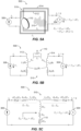
- a technique that combines several advantages as previously discussed with reference to FIGs. 4A and 5A and that avoids certain issues related to blind spots as previously discussed with reference to FIGs. 6A and 6C is illustrated by the circuit 800 of FIG. 8A .
- This technique is referred to as capacitively compensated mutual impedance sensing.
- the circuit 800 is also based on the current source voltage measurement approach.
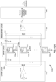
- a sense coil arrangement 510 is used for sensing the object 110.
- the sense coil arrangement 510 includes a primary sense coil 512 with inductance L 1 and a secondary sense coil 514 with inductance L 2 , each having a first and second terminal.
- the circuit 800 further includes a capacitor 820 (compensation or tuning capacitor) with capacitance C.
- the capacitor 820 has a first and second terminal.
- the first terminal of the capacitor 820 is electrically connected to the second terminals of each of the sense coils 512 and 514.
- the circuit 800 includes an alternating current source 306 that is tunable in frequency and that drives a current I 1 at sense frequency f s into the primary sense coil 512.
- the current source 306 is electrically connected to the first terminal of the primary sense coil 512 and to the second terminal of the capacitor 820 (in some implementations the second terminal of the capacitor 820 is electrically connected to a reference ground potential).
- the voltage measurement circuit 304 is electrically connected to the first terminal of the secondary sense coil 514 and to the second terminal of the capacitor 820.
- the voltage measurement circuit 304 may be frequency selective (narrowband) tuned to the sense frequency f s .
- FIG. 8A also indicates presence of materials 310 by the shaded area.
- FIG. 8B An equivalent circuit of the circuit 800 of FIG. 8A including a circuit model of the object 110 is shown in FIG. 8B .
- the primary sense coil 512 and secondary sense coil 514 are each represented by an equivalent inductance L 1 and L 2 , respectively, and by an equivalent loss resistance R 1 and R 2 .
- each of these elements may be a function of temperature ⁇ .
- the equivalent loss resistances R 1 and R 2 may each include a first resistance component due to losses in the sense coil's conductive structure (e.g., copper wires or PCB traces) and a second resistance component due to loss effects in materials 310 as previously discussed in connection with FIG. 3B .
- Magnetic coupling between sense coils 512 and 514 is represented by a complex coupling factor k 12 , which may be also a function of temperature ⁇ as previously explained in connection with FIGs. 5B and 5C .
- the equivalent inductances and resistance L 1 , L 2 , R 1 and R 2 , respectively, as well as the coupling factor k 12 may include a change due to the presence of materials 310. Since the electromagnetic properties of materials 310 may generally be temperature dependent, some temperature dependence may be expected for the coupling factor k 12 .
- the change in k 12 due to materials 310 may include a real and imaginary component due to reactive and resistive (loss) effects, respectively, in materials 310 but also due to mutual loss effects in the sense coils 512 and 514 as previously discussed.
- the real component relates to the mutual inductance M 12 defined by Equation (29) while the imaginary component relates to an equivalent mutual resistance R 12 defined by Equation (31).
- FIG. 8B shows each of the primary sense coil 512 and the secondary sense coil 514 magnetically coupled with coupling factor k 13 and k 23 , respectively, to the object 110 represented by an LR-Model ( L 3 , R 3 ) as previously discussed e.g., with reference to FIG. 3B .
- the compensation capacitor appears with its equivalent capacitance C that may be also a function of temperature ⁇ depending on the type of capacitor as previously discussed in connection with FIG. 4A .
- FIG. 8C shows a simplified equivalent circuit of the circuit 800 of FIG. 8A .
- the sense coil arrangement 512 is represented by a simplified "T" equivalent circuit model neglecting first and second series branch impedance as previously discussed with reference to FIG. 6B .
- This simplified equivalent circuit solely comprises the shunt branch impedance that is now referred to as the capacitively compensated mutual impedance Z 12 c . It includes the mutual inductance M 12 , the equivalent mutual resistance R 12 , the capacitance C that appears now in series to mutual inductance M 12 , and the equivalent mutual impedance change ⁇ Z 12 that represents the object 110 abstracted away.
- This condition may also be considered as some sort of resonance and may be achieved by tuning the frequency f s of the current source so that the magnitude of the mutual impedance Z 12 c in absence of the object 110 denoted by
- equation (74) may be rewritten as ⁇ Z 12 Z 12 c , 0 ⁇ k 13 k 23 k _ 12 Q 12 1 Q 3 ⁇ j showing that the fractional change
- Equation (75) may be rewritten as ⁇ Z 12 Z 12 c , 0 ⁇ k 13 2 Q 12 1 Q 3 ⁇ j
- Equation (29) Equation (29)
- M 12 ⁇ L 1 L 2
- Equation (73) Equation (73)
- each of the sense coils 512 and 514 of the circuit 800 of FIG. 8A identical (or substantially similar) to the sense coil 302 of the circuit 400 of FIG.
- This loss resistance component may be diminished by keeping a small vertical distance between the two sense coils 512 and 514 ( e.g., in sense coil arrangement 510 of FIG. 5F ) such that
- a small vertical distance between the two sense coils 512 and 514 is provided to diminish the loss resistance.
- a gain in Q-factor by a factor of four was found in a non-optimized experimental set-up integrated into a wireless power transfer structure 236 using identical sense coils with equal length lead lines for all sense coils 512, 514, and 302.
- mutual impedance measurement may be subjected to measurement errors.
- reactance compensation e.g ., in the circuit 400 of FIG. A
- mutual reactance compensation may provide a mechanism for accurate calibration of the mutual impedance measurement e.g ., with respect to the angle arg ⁇ Z 12 c ⁇ for purposes as previously discussed in connection with the circuit 300 of FIG. 3A .
- compensation capacitor 820 together with current source 306 and a voltage measurement circuit 304 each presenting a high input impedance at sense frequency f s and a low impedance at low frequencies may form a high pass filter to attenuate low frequency signal components e.g ., at the wireless power transfer frequency f wpt as described in more detail in connection with FIG. 12 .
- This may result in relaxed requirements for the voltage measurement circuit 304 and the current source 306 with respect to the dynamic range, overvoltage capability, etc. as previously discussed in connection with the circuit 400 of FIG. 4A .
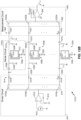
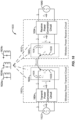
- FIG. 9 is a block diagram of a circuit 900 illustrating example implementations or operations of an object detection circuit 100.
- the block diagram may apply to any of the impedance and transimpedance (e.g., mutual impedance) sensing techniques and variants thereof as described with reference to FIGs. 3A to 8A as well as to various impedance or transimpedance measurement approaches (e.g., the current source voltage measurement approach as previously described with reference to FIG. 3A and 5A ).
- the circuit 900 includes a driver circuit 910, a control circuit 950 associated with the driver circuit 910, a plurality of sense circuits 104, a measurement circuit 920, and a control, processing & evaluation circuit 960 associated with the measurement circuit 920.
- Each sense element may include one or more sense coils (e.g., a sense coil arrangement 510 as it may be required by some of the mutual impedance sensing techniques as previously described with reference to FIGs. 5A to 8A ).
- the plurality of sense elements 106a, 106b, ..., 106n may be arranged in an array ( e.g ., array 106 as previously described with reference to FIGs. 1 and 2A ).
- the object detection circuit 100 of FIG. 1 using capacitive compensation of an impedance or a mutual impedance as described with reference to FIGs.
- each of the plurality of the sense circuits 104a, 104b, ..., 104n may include a compensation (tuning) capacitor (e.g ., capacitor 420 or 820 as shown in FIG. 4A or 8A , respectively).
- Each of the plurality of sense circuits 104a, 104b, ..., 104n may be tuned substantially to a nominal sense frequency. In some implementations, there is a nominal sense frequency common to each of the plurality of sense circuits 104a, 104b, ..., 104n. In other implementations, sense circuits of the plurality of sense circuits 104a, 104b, ..., 104n are intentionally or unintentionally tuned to different nominal sense frequencies.
- the driver circuit 910 (e.g., a portion of the current source 306 with reference to FIG. 3A ) is electrically connected to the plurality of sense circuits 104a, 104b, ..., 104n.
- the driver circuit 910 is configured to operate as a current source (e.g., current source 306 as described in connection with FIG. 3A ) and selectively ( e.g., sequentially) apply a sense current signal I 1 (as indicated in FIG. 9 ) at an operating (sense) frequency f s to each of the plurality of sense circuits 104a, 104b, ..., 104n.
- the driver circuit 910 is configured to operate as a voltage source e.g ., as described in connection with FIG. 3A and selectively ( e.g ., sequentially) apply a sense voltage signal V 1 (as indicated in FIG. 9 ) at an operating (sense) frequency f s to each of the plurality of sense circuits 104a, 104b, ..., 104n.
- the driver circuit 910 is configured to operate as a source that may be characterized neither by a current source nor a voltage source.
- the driver circuit 910 may generate a sinusoidal sense signal with a defined frequency, amplitude and phase.
- the following descriptions of the circuit 900 of FIG. 9 assume a sinusoidal sense signal.
- other sense signal waveforms may be used in certain implementations as previously discussed in connection with FIG. 3A .
- the driver circuit 910 may be configured to generate and apply more than one sense signal (e.g., sense current signal I 1 ) at a time as it may be required in some implementations or operations of an object detection circuit 100.
- the concurrently applied sense signals may generally differ in frequency and amplitude.
- a driver circuit 910 capable of concurrently generating and applying a plurality of sense signals with different (distinct) sense frequencies f s may be used in some implementations or operations of the object detection circuit 100 e.g., to expedite an impedance measurement in each of the plurality of sense circuits 104a, 104b, ..., 104n and/or to expedite a transimpedance measurement in each of a plurality of sense circuit pairs e.g ., in an implementation where each sense circuit includes a single sense coil ( e.g ., sense coil 512 or 514) as discussed with reference to FIG. 5D .
- each sense circuit includes a single sense coil (e.g ., sense coil 512 or 514) as discussed with reference to FIG. 5D .
- a driver circuit 910 configured to provide two outputs (e.g ., current source outputs) each delivering a sinusoidal signal (e.g ., sense current signal I 1 ) with the same frequency f s but generally different amplitude and phase may be used to accomplish flux balanced mutual impedance sensing as described with reference to FIG. 7A .
- An example implementation of a driver circuit 910 configured to provide two current source outputs delivering respective current signals I 1 a and I 1 b is illustrated by FIG. 11 .
- a control circuit 950 electrically connected to the driver circuit 910 is shown for illustrative purposes to indicate control of the driver circuit 910.
- the measurement circuit 920 is electrically connected to each of the plurality of sense circuits 104a, 104b, ..., 104n.
- the measurement circuit 920 is configured to selectively ( e.g ., sequentially) measure an electrical voltage V 2 (as indicated in FIG. 9 ) in each of the plurality of sense circuits 104a, 104b, ..., 104n and to provide a measurement output V out proportional to the electrical voltage V 2 .
- the measurement output V out is proportional to an electrical voltage V 2 in one of the plurality of sense circuits 104a, 104b, ..., 104n in response to the at least one sense current signal I 1 being applied by the driver circuit 910 to the respective at least one sense circuit of the plurality of sense circuits 104a, 104b, ..., 104n.
- the measurement circuit 920 is configured to selectively ( e.g ., sequentially) measure an electrical current I 2 (as indicated in FIG. 9 ) in each of the plurality of sense circuits 104a, 104b, ..., 104n and to provide a measurement output V out proportional to the electrical current I 2 .
- the measurement output V out is proportional to an electrical current I 2 in one of the plurality of sense circuits 104a, 104b, ..., 104n in response to the at least one sense voltage signal V 1 being applied by the driver circuit 910 to the respective at least one sense circuit of the plurality of sense circuits 104a, 104b, ..., 104n.
- the measurement circuit 920 is an analog front-end portion of a more complex measurement circuit that also encompasses functions included in the control, processing & evaluation circuit 960.
- the measurement circuit 920 may include a multiplexer (e.g ., multiplexer 922) and an amplifier (e.g ., amplifier 924) as illustrated in FIG. 9 by dashed lines.
- the measurement circuit 920 is configured to measure more than one voltage V 2 or current I 2 at a time and to provide more than one respective measurement output V out .
- Concurrent multiple voltage or current measurement may be required in some implementations or operations of the object detection circuit 100 e.g., to expedite an impedance and/or a transimpedance and/or a flux compensated mutual impedance measurement in each of the plurality of sense circuits 104a, 104b, ..., 104n and/or in pairs and/or even in triples of sense circuits, respectively, of the plurality of sense circuits 104a, 104b, ..., 104n as previously discussed in the context of the driver circuit 910.
- measurement of a plurality of voltages V 2 or currents I 2 is performed concurrently and frequency selectively at the respective frequency f s of each of the plurality of sense signals I 1 or V 1 that is selectively applied to the plurality of sense circuits 104a, 104b, ..., 104n.
- a control, processing & evaluation circuit 960 electrically connected to the measurement circuit 920 is shown for illustrative purposes to indicate control of the measurement circuit 920 and the further processing.
- FIG. 9 assume example implementations based on the current source voltage measurement approach as described with reference to FIG. 3A . However, this should not exclude other impedance or transimpedance measurement approaches (e . g ., voltage source current measurement approach) that may apply.
- impedance or transimpedance measurement approaches e . g ., voltage source current measurement approach
- the driver circuit 910 is configured to operate as at least one current source (e.g., characterized by a quasi-ideal current source as previously defined in connection with FIG. 3A ) and selectively (e.g., sequentially) apply at least one sense current signal I 1 with a defined amplitude and phase at an operating frequency (sense frequency) f s to each of the plurality of sense circuits 104a, 104b, ..., 104n.
- a current source e.g., characterized by a quasi-ideal current source as previously defined in connection with FIG. 3A
- selectively e.g., sequentially
- apply at least one sense current signal I 1 with a defined amplitude and phase at an operating frequency (sense frequency) f s to each of the plurality of sense circuits 104a, 104b, ..., 104n.
- only one sense circuit of the plurality of sense circuits 104a, 104b, ..., 104n is driven at a time.
- the driver circuit 910 may include components such as at least one signal source 912 (e.g., generating the sinusoidal sense signal with a defined frequency f s , amplitude and phase), at least one driver amplifier circuit 914, and at least one multiplexer circuit 916 also referred to as the input multiplexer.
- the at least one driver amplifier circuit 914 is configured to provide a current source output characterized e.g., as a quasi-ideal current source suitable for selectively driving each of the plurality of sense circuits 104a, 104b, ..., 104n based on a signal received from the respective signal source 912.
- the at least one multiplexer circuit 916 may be electrically connected between the output of the respective driver amplifier circuit 914 and the plurality of sense circuits 104a, 104b, ..., 104n and is configured to selectively connect each of the plurality of sense circuits 104a, 104b, ..., 104n to the output of the respective driver amplifier circuit 914.
- the driver circuit 910 may also return at least one reference signal to the control circuit 950. This at least one reference signal may be representative for the respective sense current signal I 1 in terms of frequency, amplitude, and phase.
- This at least one reference signal may be used in the control, processing & evaluation circuit 960 e.g., for computing at least one ratio V out / I 1 (complex value) that may relate to an impedance or a transimpedance ( e . g. , a mutual impedance).
- the control, processing & evaluation circuit 960 may be configured to provide analog-to-digital signal conversion, frequency selective filtering, synchronous detection, combining outputs, summation of outputs, averaging of outputs, scaling of outputs, correction of outputs, evaluation of sequences (time-series) and/or patterns of outputs indicative of an impedance and/or transimpedance ( e.g ., mutual impedance), etc. and eventually to decide whether an object (e.g ., object 110 of FIG.
- 3A is proximate to at least one sense element of the plurality of sense elements 106a, 106b, ..., 106n based on a change in an impedance or transimpedance (e.g., mutual impedance) and to output at least a detection hypothesis H out as indicated in FIG. 9 .
- an impedance or transimpedance e.g., mutual impedance
- the detection hypothesis H out may be indicative for presence or absence of an object (e.g., object 110) and may be used by the wireless power transfer system 200 with reference to FIG. 2A to control wireless power transfer.
- a positive detection hypothesis H out may be indicative for presence of an object (e.g., object 110) and may cause the wireless power transfer system 200 to cease wireless power transfer or to reduce a level of power.
- a negative detection hypothesis H out may be indicative for absence of an object and may cause the wireless power transfer system 200 to continue or resume wireless power transfer or to return to the ordinary power level.
- the detection hypothesis output H out may include additional information (e.g., the position of the at least one sense element associated to a positive hypothesis output H out and/or a detection confidence value).
- the control, processing & evaluation circuit 960 processes at least one sequence (time-series) of consecutive measurement outputs V out each associated to the same at least one sense circuit (e.g ., sense circuit 104a or pair of sense circuits 104a and 104b) of the plurality of sense circuits 104a, 104b, ..., 104n to determine a level of correlation between the at least one first sequence of consecutive measurement outputs V out and a corresponding second sequence indicative of the applied exposure magnetic field signal. Presence of an object (e . g ., object 110) is assumed if the level of correlation exceeds a threshold for at least one sense circuit or at least one pair of sense circuits of the plurality of sense circuits 104a, 104b, ..., 104n.
- Presence of an object e . g ., object 110
- Presence of an object is assumed if the level of correlation exceeds a threshold for at least one sense circuit or at least one pair of sense circuits of the plurality of sense circuits 104
- inductive ferromagnetic sensing is combined with a space-differential detection scheme. Presence of an object (e.g ., object 110) is assumed if at least one difference between the correlator output associated to at least one first sense circuit (e.g ., sense circuit 104a) and the correlator output associated to at least one second sense circuit (e.g ., sense circuit 104b) exceeds a threshold. In another example implementation or operation, respective correlator outputs obtained with inductive ferromagnetic sensing and with inductive thermal sensing are combined.
- Inductive kinematic sensing may be a further specialized detection scheme for detecting an object (e.g., object 110) by its relative motion e.g., when the object is mechanically moved relative to the sense elements (e.g ., the plurality of sense elements 106a, 106b, ..., 106n).
- the top surface of the housing 236 of the wireless power transfer structure 224 where an object may rest is mechanically moved back and forth relative to the sense element array 106.
- the relative movement of an object (e.g., object 110) in proximity of a sense element (e.g., sense element 106a) may produce a time-varying change in an electrical characteristic (e.g., impedance Z 1 , mutual impedance Z 12 ) and thus in the measurement output V out .
- an electrical characteristic e.g., impedance Z 1 , mutual impedance Z 12
- this change (response) in an electrical characteristic will generally be a function of the object's instantaneous position relative to the sense element array 106. This function may be a non-linear function.
- presence of an object is determined based on a correlation between the at least one first sequence of consecutive measurement outputs V out each associated to the same at least one sense circuit (e.g., sense circuit 104a or pair of sense circuits 104a and 104b) of the plurality of sense circuits 104a, 104b, ..., 104n and a corresponding second sequence indicative of the mechanical movement signal.
- sense circuit 104a or pair of sense circuits 104a and 104b e.g., sense circuit 104a or pair of sense circuits 104a and 104b
- Inductive kinematic sensing may potentially provide a solution for detecting objects of any category e.g ., as described with reference to FIG. 3D on an absolute basis as defined above.
- the control, processing & evaluation circuit 960 processes at least one first sequence of consecutive measurement outputs V out each associated to the same at least one sense circuit (e.g., sense circuit 104a or pair of sense circuits 104a and 104b) of the plurality of sense circuits 104a, 104b, ..., 104n to determine a level of correlation between the at least one first sequence of consecutive measurement outputs V out and a corresponding second sequence indicative of the mechanical movement signal. Presence of an object (e.g ., object 110) is assumed if the level of correlation exceeds a threshold for at least one sense circuit or at least one pair of sense circuits of the plurality of sense circuits 104a, 104b, ..., 104n.
- Presence of an object e.g ., object 110
- inductive kinematic sensing is combined with a space-differential detection scheme. Presence of an object (e.g., object 110) is assumed if at least one difference between the correlator output associated to at least one first sense circuit (e.g ., sense circuit 104a) and the correlator output associated to at least one second sense circuit (e.g ., sense circuit 104b) exceeds a threshold.
- correlator outputs obtained with inductive kinematic sensing, inductive thermal sensing, and inductive ferromagnetic sensing are combined.
- an object detection circuit 100 In some implementations or operations of an object detection circuit 100, one or more specialized detection schemes as described above are applied initially before starting regular wireless power transfer e.g ., for the purpose of charging an electric vehicle. If the object detection circuit 100 determines presence of an object (e.g ., object 110), the wireless power transfer system 200 stops detection based on a specialized detection scheme and does not start regular wireless power transfer. During regular wireless power transfer, the object detection circuit 100 may employ at least one other detection scheme e.g., a time-differential scheme capable of detecting an object ( e.g. , object 110) when it enters the predetermined space.
- a time-differential scheme capable of detecting an object (e.g. , object 110) when it enters the predetermined space.
- one or more specialized detection schemes as described above are applied in the event that the object detection circuit 100 trips during regular wireless power transfer.
- one or more specialized detection schemes may be used to verify this detection by first ceasing regular power transfer and then reapplying one or more specialized detection schemes. This may apply in case of a detection with low confidence. If the previous finding of presence of an object (e.g ., object 110) is confirmed, the wireless power transfer system 200 discontinues regular wireless power transfer else it reactivates regular wireless power transfer.
- control circuit 950 and/or the control, processing & evaluation circuit 960 are configured to perform calibration for purposes of determining reference values as previously described for purposes of threshold detection. In further aspects, they may be configured to perform calibration of the impedance or transimpedance measurement with respect to the angle (e.g., arg ⁇ Z 1 ⁇ ) as previously described with reference to the circuit 300 of FIG. 3A .
- control circuit 950 and/or the control, processing & evaluation circuit 960 are configured to perform functions such as finding optimum sense frequencies f s minimizing the effect of circuit extrinsic noise as previously described with reference to the circuit 300 of FIG. 3A .
- the driver circuit 910 is configured to concurrently generate and selectively (e.g., sequentially) apply a plurality of current signals I 1 each with a distinct frequency f s .
- Each of the plurality of current signals I 1 is selectively ( e.g ., sequentially) applied to each of a subset of the plurality of sense circuits 104a, 104b, ..., 104n.
- the number of subsets may equal the number of concurrently applied current signals I 1 .
- such multiple current signal operation may be used to expedite impedance and/or transimpedance measurements in each of a plurality of sense circuits and/or in each of a plurality of pairs of sense circuits, respectively, of the plurality of sense circuits 104a, 104b, ..., 104n.
- an intermodulation product generated by the first and second current signal I 1 having a first and second frequency f s may fall onto the third frequency f s of the third current signal I 1 , thus interfering e.g., in the measurement circuit 920 with the voltage signal V 2 in response to the third current signal I 1 .
- Interference caused by intermodulation products generally manifests in variations in a sequence (time-series) of consecutive measurement outputs V out associated to the same at least one sense circuit (e.g ., sense circuit 104a or pair of sense circuits 104a and 104b). If measurement outputs V out refer to an output (not shown in FIG.
- these variations may be generally characterized by variations in a magnitude and phase. These variations may resemble the effects of circuit intrinsic or extrinsic noise sources as previously discussed with reference to FIG. 3A . However, the variance caused by intermodulation interference may be significantly larger than that produced e.g. , by circuit intrinsic noise. These variations may require the detection threshold to be increased e.g ., in an implementation or operation based on a time-differential detection scheme as described below, thus resulting in lower detection sensitivity.
- interference caused by intermodulation effects is mitigated by a smart selection of sense frequencies f s e.g., by selecting a set of frequencies whose intermodulation products (e.g., up to the fourth order) do not fall on any of the frequencies f s of the selected set of frequencies.
- this approach may put some constraints on the choice of sense frequencies f s .
- the number of concurrently applied currents I 1 is greater than three and in implementations or operations where sense circuits have to be operated at or near resonance, have tolerances with respect to the resonant frequency, and where some frequency bands e.g., jammed by frequency selective switching noise have to be avoided for purposes as previously discussed.
- interference due to intermodulation effects is mitigated by choosing sense frequencies f s for the plurality of concurrently applied current signals I 1 from a set of frequencies with a fixed frequency spacing ⁇ f (e.g., a frequency grid).
- each sense frequency f s is a multiple of the frequency spacing ⁇ f (e.g., 1 kHz). It may be appreciated that the plurality of current signals I 1 with sense frequencies f s differing by integer multiples of ⁇ f generates intermodulation products with frequencies that are also an integer multiple of ⁇ f , thus may potentially fall on one or more sense frequencies f s .
- phase of each of the plurality of concurrently applied current signals I 1 is controlled in a manner so that any intermodulation product falling on a sense frequencies f s produces a static offset (instead of noise-like variations) in sequences (time-series) of consecutive measurement outputs V out associated to the same at least one sense circuit (e.g., sense circuit 104a or pair of sense circuits 104a and 104b).
- a small static offset e.g ., equivalent to a fractional change below 1%) as it may be caused by intermodulation effects may not negatively impact operation of an object detection circuit 100. This may be particularly true for implementations or operations employing a time-differential detection scheme.
- control, processing & evaluation circuit 960 is configured to use the extracted low frequency component as supplementary information being indicative of presence and level of the low frequency magnetic field at wireless power transfer frequency f wpt e.g., to improve the evaluation of measurement outputs V out to determine presence of an object (e.g., object 110).
- this improvement may include adaptation of a threshold e.g., to reduce a false detection rate e.g., due to external noise at sense frequency f s generated by the power conversion circuit 222 with reference to FIG. 2A , which may accompany the low frequency magnetic field.
- the component at f wpt in the voltage V 2 across the sense circuit (e.g., sense circuit 104a) may be only 30 mV while the wanted signal component at sense frequency f s may be in the order of 100 mV.
- the second capacitor 1006 may be needed in some implementations to block any residual DC flow at the output of the driver circuit 910 ( e.g., due to a DC offset).
- the capacitor 1006 may also help to attenuate any residual low frequency current component ( e.g., at a wireless power frequency f wpt ) at the output of the driver circuit 910.
- the third capacitor 1010 may be needed in some implementations to block any residual DC flow at the input of the measurement circuit 920 ( e.g., due to a DC offset).
- the capacitor 1010 may also help to attenuate any residual low frequency current component (e.g., at a wireless power frequency f wpt ) at the input of the measurement circuit 920. Moreover, in some implementations, it may be also used to compensate or partially compensate for the effect of the reactance of shunt inductor 1008 in the measured impedance Z 1 c .
- series resistor 1018 with a large enough resistance R ser 1 potentially transforms the voltage source output (virtually zero source impedance) of the driver amplifier circuit 914 into a quasi-ideal current source 306 (high source impedance) with reference to FIG. 3A .
- a series resistor 1018 with a very large resistance R ser 1 may provide an almost ideal current source characteristic but may also result in a too low sense current I 1 and thus in insufficient SNR as it may be seen from Equation (58). Therefore, in some implementations, the resistance R ser 1 may be a trade-off between the quality of the current source ( e.g ., as specified with reference to FIG. 3A ) and the resulting SNR.
- the numerical result of Equation (82) indicates that this example implementation of a driver circuit 910 satisfies the requirements specified by Equation (2).
- the driver circuit 910 has the potential to drive more than one sense circuit with a current I 1 at a time, each having the same frequency f s and substantially the same amplitude and phase. If e.g. , switch 1016a and 1016b are closed, each of the sense circuits 104a and 104b is driven with a current I 1 .
- the input multiplexer circuit 916 includes a plurality of switches 1016a, 1016b, ..., 1016n and is configured to selectively connect each of the plurality of sense circuits 104a, 104b, ..., 104n via series resistor 1018 to the driver amplifier circuit 914 to selectively ( e.g ., sequentially) drive each of the plurality of sense circuits 104a, 104b, ..., 104n with a sense current I 1 at a sense frequency f s . Therefore, each of the plurality of switches 1016a, 1016b, ..., 1016n is electrically connected to a common input node that is electrically connected to the output of the driver amplifier circuit 914.
- Each of the plurality of switches 1016a, 1016b, ..., 1016n may be one of a semiconductor analog switch (e.g ., a single FET switch, a complementary FET switch composed of a p-channel and a n-channel type FET), a micro-mechanical (MEMS) switch or any other type of switch providing a sufficiently high current signal attenuation in the off-state.
- An analog switch e.g ., a complementary FET switch
- An analog switch may be modelled by an on-state series resistance R sw , an off-state series capacitance C sw , a first and a second parasitic shunt capacitance C sh 1 and C sh 1 , respectively, as indicated in FIG.
- the total capacitive load produced by the plurality of first shunt capacitances C sh 1 may not noticeably impair the current source characteristic of the driver circuit 910 since it is in parallel to the voltage source output (virtually zero source impedance) of the driver amplifier circuit 914. This may be true as long as the operational amplifier 1015 can handle the resulting total capacitive load. Assuming operations where only one or a few switches of the plurality of switches 1016a, 1016b, 1016n are closed at a time, the total capacitive load at the common input node is governed by the plurality of first capacitances C sh 1 .
- an operational amplifier 1025 e.g., a low noise operational amplifier
- This circuit transforms an input current I in into an output voltage V out proportional to I in . Since the voltage at the negative input of operational amplifier 1025 is virtually zero (virtual ground), the measurement amplifier circuit 924 exhibits a virtually zero input impedance.
- the measurement amplifier circuit 924 together with series resistors 1021 mimic a quasi-ideal voltage measurement circuit 304 with reference to FIG. 3A to selectively ( e.g ., sequentially) measure the electrical voltage V 2 at each of the plurality of sense circuits 104a, 104b, ..., 104n.
- series resistor 1021 with a large enough resistance R ser 2 potentially transforms the quasi-zero impedance input of the measurement amplifier circuit 914 into a high impedance input as required for a quasi-ideal voltage measurement circuit 304 with reference to FIG. 3A .
- a series resistor 1021 with a very large resistance R ser 2 may provide an almost ideal measurement circuit but may also result in a lower current I in and thus in insufficient SNR with respect to the measurement circuit's 920 intrinsic noise.
- Increasing resistance R ser 2 also requires the feedback resistance R f to be increased if a specified voltage gain of the measurement circuit 960 needs to be met.
- the resistance R ser 2 may be a trade-off between the quality of the voltage measurement (as defined with reference to FIG. 3A ), resulting SNR, and stability conditions.
- V out refers to the measurement output of the measurement circuit 920 (quasi-ideal voltage measurement circuit with a finite input impedance) and V out , ⁇ to the measurement output of an ideal voltage measurement circuit (infinite input impedance) but the same voltage gain.
- Equation (83) indicates that this example implementation of a measurement circuit 920 satisfies the requirements specified by Equation (3).
- the measurement circuit 920 has the potential to measure the sum voltage of two or more electrical voltages V 2 at a time since it is configured as a summation amplifier.
- Series resistor 1021 transforms the voltage V 2 into a corresponding current at the common output node (input of the measurement amplifier circuit 924). If e.g., switch 1023a and switch 1023b are closed, the measurement output V out is proportional to the sign inverse of the sum of the voltage V 2 at sense circuit 104a and sense circuit 104b, since currents V 2 / R ser 2 resulting at the common output node add up.
- the output multiplexer circuit 922 including the plurality of switches 1023a, 1023b, ..., 1023n is configured to selectively connect each of the plurality of sense circuits 104a, 104b, ..., 104n via series resistor 1021 to the measurement (transimpedance) amplifier circuit 924 to selectively (e.g ., sequentially) measure an electrical voltage V 2 at each of the plurality of sense circuits 104a, 104b, ..., 104n in response to a current I 1 at a sense frequency f s . Therefore, each of the plurality of switches 1023a, 1023b, ..., 1023n is electrically connected to a common output node that is electrically connected to the input of the measurement amplifier circuit 924.
- each of the plurality of switches 1023a, 1023b, ..., 1023n may be one of a semiconductor analog switch (e.g., a single FET switch, a complementary FET switch composed of a p-channel and a n-channel type FET), a micro-mechanical (MEMS) switch or any other type of switch providing a sufficiently high current signal attenuation in the off-state.
- a semiconductor analog switch e.g., a single FET switch, a complementary FET switch composed of a p-channel and a n-channel type FET
- MEMS micro-mechanical
- each switch of the input multiplexer 916 (plurality of switches 1016a, 1016b, ..., 1016n) and a different (non-corresponding) switch of the output multiplexer 922 (plurality of switches 1023a, 1023b, ..., 1023n) are closed sequentially in a round robin fashion.
- a first input multiplexer switch e.g ., switch 1016a
- a non-corresponding output multiplexer switch e.g ., switch 1023b
- all other switches are open.
- a second input multiplexer switch (e.g.
- this high pass filter may substantially reduce dynamic range requirements in the measurement circuit 920 and in a further processing (e.g., ADC) e.g., as part of the control, processing & evaluation circuit 960 with reference to FIG. 9 .
- the shunt inductor 1008 may also reduce any cross-modulation effects between any low frequency signals at the wireless power transfer frequency f wpt and harmonics thereof and the sense signal at frequency f s ( e.g., in the MHz range). Cross-modulation may be produced by residual non-linear effects in the measurement circuit 920.
- transformer 1328 of the measurement circuit 920 may be configured to provide a relatively low main inductance that appears in parallel to (across) the series circuit of capacitor 820 and the secondary sense coil 514 of the selected sense circuit (e.g ., sense circuit 104a) to more effectively attenuate any signal component at the wireless power transfer frequency f wpt and low frequency harmonics thereof in the electrical voltage V 2 at the input of the voltage measurement amplifier circuit 920.
- the circuit 1300 may provide similar attenuation to the circuit 1200 of FIG. 12 using capacitor 820 and shunt inductor 1008.
- these high pass filters that are effective at the common input and output of the plurality of sense circuits 104 may exert a minor impact on the transimpedance measurement and may be corrected (compensated for) in a further processing (e.g. , in the control, processing & evaluation circuit 960 with reference to FIG. 9 ). Any phase shift caused by these high pass filters may be determined e.g ., by performing a transimpedance calibration with respect to the angle e.g., arg ⁇ Z 12 c ⁇ as previously mentioned with reference to FIGs. 8A and 9 .
- the second capacitor 1006 may be needed in some implementations to block any residual DC flow at the output of the driver circuit 910 ( e.g., due to a DC offset).
- the capacitor 1006 may also help to attenuate any residual low frequency current component (e.g ., at a wireless power frequency f wpt and low frequency harmonics thereof) at the output of the driver circuit 910.
- the third capacitor 1010 may be needed in some implementations to block any residual DC flow at the input of the measurement circuit 920 ( e.g., due to a DC offset).
- the capacitor 1010 may also help to attenuate any residual low frequency voltage component (e.g. , at a wireless power frequency f wpt and low frequency harmonics thereof) at the input of the measurement circuit 920.
- the capacitor 1010 may be also used to compensate or partially compensate for the effect of the reactance of the transformer's 1328 main inductance in the measured transimpedance Z 12 c .
- capacitors 820, 1006, and 1010 may be of a type with a low temperature coefficient providing high thermal stability (e.g. , a NP0-type capacitor) reducing thermal drift of the transimpedance (e.g. , capacitively compensated mutual impedance) as measured e.g. , in each of the plurality of sense circuits 104a, 104b, ..., 104n including capacitor 820.
- high thermal stability e.g. , a NP0-type capacitor
- the transimpedance e.g. , capacitively compensated mutual impedance
- capacitors 820, 1006, 1010, series resistors 1018 and 1328, and transformers 1318 and 1328 are common to the plurality of sense circuits 104a, 104b, ..., 104n, which may provide a BOM cost advantage over the circuit 1200 of FIG. 12 .
- the method 1400 further includes measuring, at a measurement circuit 920, an electrical characteristic at an output electrically connected to a first terminal of a secondary sense coil 514, a second terminal of the secondary sense coil electrically connected to the first terminal of the capacitor 820.
- the method 1400 further includes detecting whether an object is in proximity to the primary or the secondary sense coil 512 and 514 based on the electrical characteristic.
- the implementations of the object detection circuit 100 of FIG. 1 described above may be implemented in the context of an inductive wireless power transfer system, and in particular a wireless electrical vehicle charging system where it may be desirable to detect objects that may experience inductive heating due to the magnetic field used for power transfer.
- FIG. 15 illustrates a wireless charging system 1500 for charging an electric vehicle in which any of the elements/functionality described with reference to FIGs. 1-14 may be implemented.
- the wireless charging system 1500 enables charging of an electric vehicle 1512 while the electric vehicle 1512 is parked so as to wirelessly couple power from a base wireless power transfer unit 1502a.
- the base wireless power transfer unit 1502a may correspond to the wireless power transfer system 200 as described with reference to FIG. 2A ( e.g., and particularly incorporate the base-side ( e.g., transmit) wireless power transfer structure 224 shown in FIG. 2A or 2B ). Spaces for two electric vehicles are illustrated in a parking area to be parked over corresponding base wireless power transfer units 1502a and 1502b.
- a local distribution center 1530 may be connected to a power backbone 1532 and configured to provide an alternating current (AC) or a direct current (DC) supply through a power link 1508 to the base wireless power transfer units 1502a and 1502b.
- Each of the base wireless power transfer units 1502a and 1502b also includes a base coil 1504 for wirelessly transferring power.
- the base coil 1504 may correspond to the coil 226 of the base wireless power transfer structure 224 as described with reference to FIG. 2A and 2B .
- any of the object detection systems described above with respect to FIGs. 1-14 may be integrated into the base wireless power transfer units 1502a and 1502b.
- the electric vehicle 1512 may include a battery unit 1518, an electric vehicle coil 1516, and an electric vehicle wireless power transfer unit 1514.
- the electric vehicle coil 1516 may correspond to the coil 266 of the wireless power transfer structure 260 with reference to FIG. 2B .
- the electric vehicle wireless power transfer unit 1514 may receive power when the electric vehicle coil 1516 is located in an electromagnetic field produced by the base coil 1504.
- the field may correspond to a region where energy output by the base coil 1504 may be captured by the electric vehicle coil 1516.
- the energy output by the base coil 1504 may be at a level sufficient to charge or power the electric vehicle battery 1518.
- Base wireless charging units may be located in a variety of locations.
- some suitable locations include a parking area at a home of the electric vehicle 1512 owner, parking areas reserved for electric vehicle wireless charging modeled after conventional petroleum-based filling stations, and parking lots at other locations such as shopping centers and places of employment.
- the wireless power transfer system 1600 further includes a wireless power receive circuit 1632.
- the wireless power receive circuit 1632 includes a receive resonant circuit 1642 including a receive coil 1638 having an inductance L2.
- the receive coil 1638 may correspond to the wireless power transfer coil 266 with reference to FIG. 2B .
- Implementations described herein may use capacitively loaded conductor loops (e.g ., multi-turn coils) forming a resonant structure that is capable of more efficiently coupling energy from a primary structure (transmitter) to a secondary structure (receiver) via a magnetic or electromagnetic near-field (e.g ., where both the transmit resonant circuit 1624 and the receive resonant circuit 1642 are tuned substantially to a common resonant frequency).
- resonant structures for coupling energy may be referred to as "magnetically coupled resonance,” “electromagnetically coupled resonance,” and/or "resonant induction.”
- a power supply 1622 (e.g., AC or DC) with a voltage V S supplies power P S to the transmit power conversion circuit 1604.
- the transmit power conversion circuit 1604 includes circuitry such as an AC-to-DC converter configured to convert power from standard mains AC to DC power at a suitable DC voltage level, and a DC-to-AC frequency converter configured to convert DC power to power at an operating frequency f wpt suitable for wireless high power transfer ( e.g., at 85 kHz).
- the transmit power conversion circuit 1604 includes an inverter amongst other circuitry for regulating the current I S drawn from the power supply 1622, the current I 1 in the transmit resonant circuit 1642, the voltage V 1 across the transmit resonant circuit 1624, and the power P 1 supplied to the transmit resonant circuit 1624.
- the transmit resonant circuit 1624 includes a tuning capacitor 1606 with capacitance C 1 in series with the transmit coil 1608 to compensate for the reactance of the transmit coil 1608 substantially at the operating frequency f wpt . When excited by a current I 1 , the transmit coil 1608 generates a magnetic field at the operating frequency f wpt .
- the transmit coil 1608 receives the power P 1 from the transmit power conversion circuit 1604 (e.g., AC current is driven into the transmit coil 1608) and wirelessly transmits power at a level sufficient to charge or power a load connected to the wireless power receive circuit 1632.
- the level of power provided wirelessly by the transmit coil 1608 may be on the order of kilowatts (kW) ( e.g ., anywhere from 1 kW to 110 kW, although actual levels may be higher or lower).
- the receive coil 1638 may be positioned within the near-field of the transmit coil 1608.
- the transmit coil 1608 and the receive coil 1638 may become wirelessly coupled ( e.g ., via a magnetic field) to one another such that power may be transferred wirelessly from the transmit coil 1608 to the receive coil 1638.
- the series capacitor 1636 with capacitance C 2 may be provided to form a receive resonant circuit 1642 with the receive coil 1638 having an inductance L 2 that resonates substantially at the operating frequency f wpt .
- the series-tuned receive resonant circuit 1642 should be construed as being exemplary and other resonant topologies may be used similarly as described with the transmit resonant circuit 1624 ( e.g., with respect to resonant circuits 1624a, 1624b, and 1624c to form any combination of parallel or series topology).
- the transmit power conversion circuit 1604 and/or the transmit resonant circuit 1624 may further include other matching and/or filter circuitry configured to match impedances between the transmit resonant circuit 1624 and the transmit power conversion circuit 1604 and provide other filter functions (e.g ., harmonics filtering). Other amplifiers/oscillators and other circuitry for driving the transmit coil 1608 with the appropriate current/voltage is also contemplated.
- the receive power conversion circuit 1634 and/or the receive resonant circuit 1642 may also include similar matching and/or filter circuitry.
- the transmit coil 1608 and the receive coil 1638 may also correspond to other forms of power transfer elements.
- the term “coil” is intended to refer to a component that may wirelessly output or receive energy for coupling to another "coil.”
- the transmit coil 1608 and the receive coil 1638 are configured as coils of wire (e.g., Litz wire) and be configured as “conductor loops", and more specifically, "multi-turn conductor loops.”
- the various operations of methods described above may be performed by any suitable means capable of performing the corresponding functions.
- the means may include various hardware and/or software component(s) and/or module(s), including, but not limited to a circuit, an application-specific integrated circuit (ASIC), or processor.
- ASIC application-specific integrated circuit
- determining encompasses a wide variety of actions. For example, “determining” may include calculating, computing, processing, deriving, investigating, looking up ( e.g., looking up in a table, a database, or another data structure), ascertaining, and the like. Also, “determining” may include receiving ( e.g ., receiving information), accessing ( e.g. , accessing data in a memory), and the like. Also, “determining” may include resolving, selecting, choosing, establishing, and the like.
- a phrase referring to "at least one of" a list of items refers to any combination of those items, including single members.
- "at least one of: a, b, or c” is intended to cover: a, b, c, a-b, a-c, b-c, and a-b-c, as well as any combination with multiples of the same element ( e.g ., a-a, a-a-a, a-a-b, a-a-c, a-b-b, a-c-c, b-b, b-b-b, b-b-c, c-c, and c-c-c or any other ordering of a, b, and c).
- DSP digital signal processor
- ASIC application specific integrated circuit
- FPGA field programmable gate array
- PLD programmable logic device
- a processor may be a microprocessor, but in the alternative, the processor may be any commercially available processor, controller, microcontroller, or state machine.
- an example hardware configuration may comprise a processing system in a wireless node.
- the processing system may be implemented with a bus architecture.
- the bus may include any number of interconnecting buses and bridges depending on the specific application of the processing system and the overall design constraints.
- the bus may link together various circuits including a processor, machine-readable media, and a bus interface.
- the bus interface may be used to connect a network adapter, among other things, to the processing system via the bus.
- the bus may also link various other circuits such as timing sources, peripherals, voltage regulators, power management circuits, and the like.
Landscapes
- Engineering & Computer Science (AREA)
- Power Engineering (AREA)
- Remote Sensing (AREA)
- Life Sciences & Earth Sciences (AREA)
- Physics & Mathematics (AREA)
- Computer Networks & Wireless Communication (AREA)
- Environmental & Geological Engineering (AREA)
- Electromagnetism (AREA)
- Geology (AREA)
- General Life Sciences & Earth Sciences (AREA)
- General Physics & Mathematics (AREA)
- Geophysics (AREA)
- Mechanical Engineering (AREA)
- Transportation (AREA)
- Geophysics And Detection Of Objects (AREA)
Description
- The present disclosure relates generally to object detection, for example, in an application for inductive power transfer. In particular, the present disclosure is directed to a circuit for measuring changes of a mutual impedance between sense coils of a plurality of sense circuits.
- Object detection may be valuable for a variety of applications, and in particular for applications where it may be useful to detect objects within a predetermined region. For example, in certain inductive power transfer applications (or other types of wireless power transfer applications) it may be useful to be able to rapidly detect foreign objects that may be present in an inductive power region and that could be susceptible to induction heating due to the high magnetic field strength in that region. In an inductive wireless electric vehicle charging (WEVC) system, magnetic flux densities above a transmit coil (e.g., a primary coil) can be at relatively high levels to allow for sufficient power transfer (e.g., for a WEVC system power may be transferred on the order of kilowatts - e.g., 3.3 kW, 11 kW, and the like). Metallic objects or other objects present in the magnetic field can experience undesirable induction heating. For this reason, foreign object detection (FOD) may be implemented to detect metal objects or other objects that are affected by a magnetic field generated by the coils of the wireless power transfer system. Solutions for improving sensitivity, cost effectiveness, accuracy, and reliability of an object detection system for various applications and such as for WEVC applications are desired.
-
US 2018/076671 A1 discloses an apparatus for detecting the presence of a foreign object within a region of wirelessly transferring power to charge an electric vehicle, including a transmitting loop structure and a receiving loop structure galvanically isolated from the transmitting loop structure. A plurality of FOD loop structures may be arranged in an array over the charging area, such that the control circuit is configured to drive each of the transmitting loop structures and detect changes in the magnitude of a first voltage in each of the receiving loop structures. - The present invention relates to an apparatus for detecting objects according to
claim 1, as well to a method for measuring changes in electrical characteristics for detecting objects according toclaim 13. - Further details of the invention are set forth in the dependent claims.
- In the figures, the third and fourth digit of a reference number identify the figure in which the reference number first appears. The use of the same reference numbers in different instances in the description or the figures indicates like elements.
-
FIG. 1 illustrates an example implementation of an object detection circuit. -
FIG. 2A is a perspective view illustrating an example implementation of a wireless power transfer system including the object detection circuit ofFIG. 1 . -
FIG. 2B is a vertical cut view illustrating a portion of the wireless power transfer system ofFIG. 2A including a portion of the object detection circuit ofFIG. 1 . -
FIG. 3A is a schematic view illustrating an example of a sense coil, an object and an associated technique based on an impedance sensing approach that may be used in conjunction with the object detection circuit ofFIG. 1 . -
FIG. 3B shows an equivalent circuit of the circuit ofFIG. 3A including a circuit model of the object. -
FIG. 3C shows another equivalent circuit of the circuit ofFIG. 3A including the influence of the object model abstracted away. -
FIG. 3D illustrates a complex impedance plane, different types of objects, and corresponding areas where changes of impedance may occur. -
FIG. 4A is a schematic view illustrating an example of a sense coil, an object, and an associated technique based on a capacitively compensated impedance sensing approach that may be used in conjunction with the object detection circuit ofFIG. 1 . -
FIG. 4B shows an equivalent circuit of the circuit ofFIG. 4A including the influence of the object model abstracted away. -
FIG. 5A is a schematic view illustrating an example of a double sense coil arrangement, an object, and an associated technique based on a mutual impedance sensing approach that may be used in conjunction with the object detection circuit ofFIG. 1 . -
FIG. 5B shows an equivalent circuit of the circuit ofFIG. 5A including a circuit model of the object. -
FIG. 5C shows a 'T'-equivalent circuit of the circuit ofFIG. 5B including the influence of the object model abstracted away. -
FIGs. 5D to 5H are schematic cut views illustrating different example implementations of the double sense coil arrangement ofFIG. 5A using planar sense coils. -
FIG. 6A is a schematic view illustrating another example of a double sense coil arrangement, an object, and an associated technique based on a flux balanced mutual impedance sensing approach that may be used in conjunction with the object detection circuit ofFIG. 1 . -
FIG. 6B shows a simplified 'T' equivalent circuit of the circuit ofFIG. 6A including the influence of the object model abstracted away. -
FIG. 6C is a schematic view illustrating a further example of a double sense coil arrangement, an object, and an associated technique based on a f a flux balanced mutual impedance sensing approach that may be used in conjunction with the object detection circuit ofFIG. 1 . -
FIG. 7A is a schematic view illustrating an example of a triple sense coil arrangement, an object, and an associated technique based on a flux balanced mutual impedance sensing approach that may be used in conjunction with the object detection circuit ofFIG. 1 . -
FIG. 7B shows an equivalent circuit of the circuit ofFIG. 7A including a circuit model of the object. -
FIG. 7C shows a simplified 'T'-equivalent circuit of the equivalent circuit ofFIG. 7B including the influence of the object model abstracted away. -
FIGs. 7D to 7H are schematic cut views illustrating different example implementations of the triple sense coil arrangement ofFIG. 7A using planar sense coils. -
FIG. 8A is a schematic view illustrating an example of a double sense coil arrangement, an object, and an associated technique based on capacitively compensated mutual impedance sensing approach that may be used in conjunction with the object detection circuit ofFIG. 1 . -
FIG. 8B shows an equivalent circuit of the circuit ofFIG. 8A including a circuit model of the object. -
FIG. 8C shows a simplified 'T'-equivalent circuit of the equivalent circuit ofFIG. 8B including the influence of the object model abstracted away. -
FIG. 9 is a generic block diagram illustrating example implementations and operations of the object detection circuit ofFIG. 1 using a plurality of sense circuits applicable to both impedance and mutual impedance sensing techniques. -
FIG. 10 is a circuit diagram illustrating an example implementation of a portion of the object detection circuit ofFIG. 1 using a plurality of sense circuits applicable to both an impedance sensing and a mutual impedance sensing approach. -
FIG. 11 is a circuit diagram illustrating another example implementation of a portion of the object detection circuit ofFIG. 1 using a plurality of sense circuits applicable to both an impedance sensing and a mutual impedance sensing approach. -
FIG. 12A is a block diagram illustrating example implementations of a portion of the object detection circuit ofFIG. 1 according to the invention and using a plurality of sense circuits applicable to the capacitively compensated mutual impedance sensing approach ofFIG. 8A . -
FIG. 12B is a circuit diagram illustrating an example implementation of the generic circuit ofFIG. 12A based on the current source voltage measurement approach. -
FIG. 13A is a circuit diagram illustrating another example implementation of a portion of the object detection circuit ofFIG. 1 using a plurality of sense circuits applicable to the capacitively compensated mutual impedance sensing approach ofFIG. 8A . -
FIG. 13B is a detail view illustrating a FET multiplexer switch cell of the circuit ofFIG. 13A . -
FIG. 14 is a flow diagram of an example of a method for detecting objects. -
FIG. 15 is a perspective view illustrating a wireless charging system for charging an electric vehicle in which any of the elements/functionality described with reference toFIGs. 1-14 may be implemented. -
FIG. 16 is a schematic view illustrating an example implementation of a portion of the wireless charging system ofFIG. 15 . - The detailed description set forth below in connection with the appended drawings is intended as a description of exemplary implementations and is not intended to represent the only implementations in which the invention may be practiced. The term "exemplary" used throughout this description means "serving as an example, instance, or illustration," and should not necessarily be construed as preferred or advantageous over other exemplary implementations. The detailed description includes specific details for the purpose of providing a thorough understanding of the exemplary implementations. In some instances, some devices are shown in block diagram form. Drawing elements that are common among the following figures may be identified using the same reference numerals.
- As mentioned above object detection (and particularly metal object detection) may be valuable for a variety of applications. For detection in a predetermined region an object detection system may include a plurality of sense elements (e.g., a planar array of sense coils) distributed across a predetermined area. The predetermined region may be defined by the space where metal objects may be found and where the magnetic flux density exceeds certain limits (e.g., a threshold determined based on what levels of temperature an
object 110 might be heated up). This is generally a three-dimensional space. The number N of sense elements may be proportional or related to the minimum size of objects that are desirable to be detected. For a system that is configured to detect small objects (e.g., the size of a paper clip), the number of sense elements may be relatively high (e.g., in the order of 400). Drive circuitry for applying sense signals to each of the sense elements, the plurality of sense circuits each including a sense element and additional elements for conditioning, as well as corresponding measurement circuitry as needed for looking for changes in electrical characteristics that may correspond to the presence of an object may be costly or complex as the number N of sense elements increases. - Aspects of implementations described herein relate to configurations for driving and measurement circuitry for one or more sense circuits that allow for higher accuracy, sensitivity, and temperature stability as needed for detecting smaller objects. Aspects described herein relate to an implementation of the
object detection circuit 100 ofFIG. 1 based on a mutual impedance sensing approach that includes a sense signal source characterized by a current source (e.g., a quasi-ideal current source) that allows for determining changes in mutual impedance based on measuring a voltage (e.g., using a quasi-ideal voltage measurement circuit) in one or more sense circuits. Aspects of implementations based on mutual impedance sensing described in detail below allows for improved detection sensitivity e.g., in presence of strong temperature variations such as they may be experienced in an outdoor environment. -
FIG. 1 illustrates an example implementation of anobject detection circuit 100 that includes a plurality of (N)sense circuits 104 illustrated inFIG. 1 bysense circuits sense circuit 104n. The plurality ofsense circuits 104 is also referred herein as to the plurality ofsense circuits FIG. 1 , each sense circuit of the plurality ofsense circuits sense elements object 110 in proximity to at least one of the plurality ofsense elements plurality sense circuit FIG. 1 ) e.g., configured to improve measurement of a change in the one or more electrical characteristics. Each of the plurality ofsense circuits FIG. 1 ) where the change in an electrical characteristic (e.g., an impedance) is measured and refers to. - Each of the plurality of
sense elements FIG. 1 as a "circular" coil for purposes of illustration. However, in other implementations, thesense elements FIG. 6C ). In yet other implementations, the plurality ofsense elements FIG. 6C ). In further implementations, the plurality ofsense elements sense elements object 110. In some implementations further described herein, each of the plurality ofsense elements FIGs. 7F to 7H ) that may be used in conjunction with a transimpedance or mutual impedance sensing approach. In some implementations, the plurality ofsense elements array 106, such as a two-dimensional array 106 as shown inFIG. 1 . However, in other implementations, the sense elements of the plurality ofsense elements sense elements array 106 and thus the number N of sense circuits can vary widely based on the application including the total region in which theobject 110 is to be detected and the smallest size of an object theobject detection circuit 100 is configured to detect. - Each of the plurality of
sense circuits sense elements detection circuit 108. The measurement anddetection circuit 108 is configured to measure one or more electrical characteristics at each of the plurality ofsense circuits object 110 is detected. In some aspect, the output may include the location of theobject 110 based on information about the particular sense element of the plurality ofsense elements object 110 is detected. The measurement anddetection circuit 108 may be configured to selectively (e.g., sequentially) apply a sense signal individually to each of the plurality ofsense circuits sense circuits object 110. The measurement anddetection circuit 108 further includes a measurement circuit to output for each of the plurality ofsense circuits - The measurement and
detection circuit 108 may include signal processing circuitry configured to process and filter the measurement output and determine whether anobject 110 is potentially present (e.g., based on a time-differential detection approach). At least a portion of the measurement anddetection circuit 108 may be implemented by one or more micro-controllers or processors. For example, at least a portion of the measurement anddetection circuit 108 may be implemented as an application-specific integrated circuit (ASIC), a field programmable gate array (FPGA) device, digital signal processor (DSP), or another processor device. The measurement anddetection circuit 108 may be configured to receive information from each of the components of theobject detection circuit 108 and perform calculations based on the received information. The measurement anddetection circuit 108 may be configured to generate control signals for each of the components that may adjust the operation of that component. The measurement anddetection circuit 108 may further include a memory (not shown) configured to store data, for example, such as instructions for causing the measurement anddetection circuit 108 to perform particular functions, such as those related to object detection. As will be described further, for purposes of selectively driving each of the plurality ofsense circuits sense circuits detection circuit 108. - In an exemplary implementation, an
object 110 is detected by applying a sinusoidal sense signal and by measuring a change of an impedance at each of the plurality ofsense circuits object detection circuit 100 may be configured to detect metallic objects (or other objects) that can cause changes in at least one of an impedance (e.g., a mutual impedance) as measured in each of the plurality ofsense circuits detection circuit 108 is configured to cause each of the plurality of sense elements (e.g., sense coils) 106a, 106b, ... , 106n (e.g., sequentially) to generate an alternating magnetic field at an operating frequency also referred herein as to the sense frequency f s. If ametallic object 110 is present in the alternating magnetic field as generated by a sense element, eddy currents will be generated in theobject 110 if the object is electrically conductive (metallic). According to Lentz' law, the eddy currents in theobject 110 will generate another (secondary) magnetic field that interacts with the respective sense element (e.g., a mutual coupling is developed). This may cause a change in an electrical characteristic (e.g., an impedance) of at least a portion of the plurality ofsense elements sense circuits object 110 and a sense element (e.g., a sense coil) of the plurality ofsense elements sense elements - In other implementations, an
object 110 is detected by applying a sense signal different from a sinusoidal signal (single frequency) and by measuring a change in a response to that signal. In an exemplary implementation, the measurement anddetection circuit 108 is configured to selectively (e.g., sequentially) excite each of the plurality ofsense elements sense circuits - In another exemplary implementation, the measurement and
detection circuit 108 is configured to selectively (e.g., sequentially) drive each of the plurality ofsense circuits sense circuits - In another exemplary implementation, the measurement and
detection circuit 108 is configured to selectively (e.g., sequentially) drive each of the plurality ofsense circuits object 110 is determined based on measuring a change in a response to that waveform in each of the plurality ofsense circuits - The descriptions of the
object detection circuit 100 herein assume a measurement anddetection circuit 100 that is configured to detect changes in an impedance at a single frequency and determine if theobject 110 is present in proximity to at least one of the plurality ofsense elements detection circuit 100 that is configured to detect changes in one or more electrical characteristics using other sense signal waveforms to determine whether anobject 110 is present. - The
object detection circuit 100 ofFIG. 1 may be used in a variety of applications for detecting objects, such as metallic objects, within a predetermined detection region as previously defined. In one example mentioned above, in an inductive wireless power transfer system, magnetic flux densities above a transmit coil (e.g., a primary coil) and below a receive coil (e.g., secondary coil) can be at relatively high levels to allow for sufficient power transfer (e.g., for a wireless electric vehicle charging (WEVC) system power may be transferred on the order of kilowatts, e.g., 3.3 kW, 11 kW, or at even higher levels). Metallic objects or other objects present in the magnetic field can experience undesirable induction heating based on interaction with the wireless power field. For this reason, theobject detection circuit 100 may be integrated into a wireless power transfer system to detect metal objects or other objects that are affected by a magnetic field generated by the coils used for the wireless power transfer. Such detection may allow the wireless power transfer system to respond appropriately (e.g., reduce or stop power transmission, alert a user, and the like). -
FIG. 2A illustrates an example implementation of a wirelesspower transfer system 200 including theobject detection circuit 100 ofFIG. 1 , apower conversion circuit 222 and a wirelesspower transfer structure 224. The wirelesspower transfer system 200 may depict either a wireless power transmit system that generates amagnetic field 232 for transferring power or a wireless power receive system that can couple and receive power via themagnetic field 232. When the wirelesspower transfer system 200 is configured as a wireless power transmit system, thepower conversion circuit 222 is configured to convert power from a power source (not shown) to a suitable operating frequency (e.g., 85 kHz) and form for wireless power transfer via the wirelesspower transfer structure 224. It may be more likely that when integrated with anobject detection circuit 100, the wirelesspower transfer system 200 may be a wireless power transmit system as power may be generally transferred from the ground or other upward facing surface where metallic objects will generally come to a rest. However other implementations are possible, e.g., theobject detection circuit 100 or a portion thereof may be also integrated into a wireless power receive system. When the wirelesspower transfer system 200 is configured as a wireless power receive system, thepower conversion circuit 222 is configured to convert power received via the wirelesspower transfer structure 224 into a suitable form (e.g., DC with a suitable voltage and current level) for providing power to a load, such as a battery. - The wireless power transfer structure 224 (also sometimes referred to as a "pad") is configured to wirelessly transmit or receive power.
FIG. 2A illustrates one example of a wirelesspower transfer structure 224 and how thesense element array 106 ofFIG. 1 may be integrated. The wirelesspower transfer structure 224 includes acoil 226 also referred to as the wireless power transfer coil that is configured to generate an alternating magnetic field when driven with a current by thepower conversion circuit 222. The wirelesspower transfer structure 224 may further includeferrite 228 configured to channel and/or provide a path for magnetic flux (e.g., may be arranged in one or more ferrite bars which can be a combination of ferrite tiles arranged to form the bars). Thepower transfer structure 224 may also include a shield 230 (also sometimes referred to as a back plate). Theshield 230 is configured to prevent themagnetic field 232 or associated electromagnetic emissions from extending beyond a boundary determined by theshield 230 or at least to attenuate themagnetic field 232 extending beyond that boundary. As an example, theshield 230 may be formed from aluminum. - In the illustrated example, the wireless
power transfer structure 224 includes a double-D (DD) coil topology, which includes two electrically conductive structures disposed proximate to one another forming the DD wirelesspower transfer coil 226. The wirelesspower transfer structure 224 is configured to generate a magnetic field (indicated inFIG. 2A by line of flux 232) by running alternating current through the DD wirelesspower transfer coil 226. Generally, the current in the two center sections of the DD wirelesspower transfer coil 226 runs in the same direction. In this way, a high magnetic flux is generated in the center of the DD wirelesspower transfer coil 226 and is channeled through theferrite 228 and arches above the DD wirelesspower transfer coil 226 from one opening (magnetic pole area) to the other opening (magnetic pole area) of the DD wirelesspower transfer coil 226 as indicated inFIG. 2A by a line of flux. Other coil topologies are also applicable to the techniques described herein, including a multi-coil topology (e.g., Bipolar, DD plus Circular) or just a single coil Circular or Solenoid topology. - The wireless
power transfer system 200 further includes theobject detection circuit 100 ofFIG. 1 that may include a plurality ofsense circuits sense elements FIG. 2A . The plurality ofsense elements planar array 106 to cover a predetermined area (e.g., at least the area covered by the wirelesspower transfer coil 226 or the ferrite 228). If each sense element of a plurality ofsense elements sense elements power transfer coil 226 or theferrite 228 and also on the smallest size of anobject 110 that is required to be detected by theobject detection circuit 100. For example, if the minimum size of ametallic object 110 required to be detected is the size of a coin (e.g., a 1 €cent coin), then the size of each sense element of the plurality ofsense elements housing 236 of the base pad as shown later inFIG. 2B ). As a mere illustrative example, the number N of sense elements of thearray 106 could be on the order of 64 (e.g., 8 × 8 array) to be able to provide coverage of the entire predetermined area with the required sensitivity. - Further the system shown in
FIG. 2A may include a housing (not shown inFIG. 2A but shown later inFIG. 2B as housing 236) configured to house, for example at least the wirelesspower transfer coil 226, theferrite 228, thesense element array 106, and potentially theshield 230. The housing may be made of any suitable material (e.g., hard plastic, ceramics etc.) and can be designed to provide structural support for example to support the weight of various objects such as vehicles that may pass over the housing. In some implementations, the housing may be made of a non-conductive material to avoid interfering or interacting with themagnetic field 232. Thesense element array 106, in one exemplary implementation, is positioned between the wirelesspower transfer coil 226 and the housing 236 (with other intervening layers if desired) so that the sense elements of the plurality ofsense elements housing 236 and where magnetic field levels could be high during power transfer. - All or just a portion of the
power conversion circuit 222 may also be housed in thehousing 236. Although in some implementations thepower conversion circuit 222 may be housed separately from thehousing 236 that houses the wirelesspower transfer structure 224. In some cases, thepower conversion circuit 222 is housed in thehousing 236 but is positioned on the other side of theshield 230 from theferrite 228. -
FIG. 2B illustrates a vertical cut view of aportion 250 of a wirelesspower transfer system 200 with reference toFIG. 2A and applicable to a WEVC application. Thisportion 250 includes the base-side (e.g., transmit) wirelesspower transfer structure 224 and the vehicle-side (e.g., receive) wirelesspower transfer structure 260. The base-side wirelesspower transfer structure 224 includes a shield (back plate) 230 made of an electrically conductive material, a layer offerrite 228 and a wirelesspower transfer coil 226. It also includes ahousing 236 configured to house the wirelesspower transfer coil 226,ferrite 228, andshield 230. In addition, thehousing 236 is configured to house asense element array 106 as part of theobject detection circuit 100 as illustrated inFIG. 2A . In some implementations, theshield 230 may form a portion of thehousing 236. Thepower conversion circuit 222 is not shown but may be electrically connected to the wirelesspower transfer coil 226 or a portion or all may also be housed in thehousing 236. - The vehicle-side wireless power receive
structure 260 includes a wirelesspower transfer coil 266, a layer offerrite 268, and ashield 270 made of an electrically conductive material. In some implementations, theshield 270 may be formed from a portion of the apparatus that theferrite 268 and the wirelesspower transfer coil 266 are affixed to (e.g., the metallic underbody of a vehicle). In this case, ahousing 276 configured to house the wirelesspower transfer coil 266 andferrite 268 is provided but that would not house theshield 270. However other implementations are possible where a shield 270 (e.g., a back plate) is included in thehousing 276. Apower conversion circuit 222 is not shown but may be electrically connected to the receivecoil 268 or a portion or all may also be housed in thehousing 276. - The base-side wireless
power transfer structure 224 may be configured to generate amagnetic field 232. The vehicle-sidewireless power structure 260 may be configured to inductively receive power via themagnetic field 232.Magnetic flux 232 may be at a particular level (flux density) at the surface of thehousing 236. In some cases, flux density may be somewhat higher at or in proximity to the top surface of thehousing 236 relative to surrounding areas as the surface of thehousing 236 is closer to the wirelesspower transfer structure 226. Furthermore, as the wirelesspower transfer structure 224 may be positioned on a ground or other top facing surface, anobject 110 may come to rest at the top surface of thehousing 236 as illustrated inFIG. 2B . Theobject 110 may thereby be potentially exposed to high levels of magnetic flux density if power is being transferred. Theobject detection circuit 100 is configured to detect theobject 110 using thesense element array 106. -
FIGs. 3 to 8 illustrate examples of different techniques based on measuring at least one electrical characteristic that may be used in conjunction with theobject detection circuit 100 ofFIG. 1 . These examples are to illustrate the principle of the sensing and measurement technique and do not show all the details of anobject detection circuit 100. Particularly, they do not show the further signal processing and evaluation circuit as it may be required e.g., for detecting an object based on a change in a measured electrical characteristic. For illustrative purposes and simplicity, these techniques are illustrated by means of a single sense element though applicable to a plurality of sense elements (e.g.,sense elements FIGs. 10 to 14 . -
FIG. 3A shows acircuit 300 to illustrate a technique for inductively sensing a presence of anobject 110 based on a change in a complex impedance Z 1 as measured at the terminals of sense coil 302 (e.g., a planar a multi-turn coil) with inductance L 1 that may represent e.g.,sense element 106a. This technique is also referred herein as to the impedance sensing approach. A change ΔZ 1 of the impedance Z 1 relative to the impedance Z 1,0 in the absence of theobject 110 may indicate a presence of theobject 110. A change of impedance may be also produced when thesense coil 302 is integrated into the wirelesspower transfer structure 224 as shown inFIG. 2A due to e.g., electrically conductive materials, ferromagnetic materials, but also due to dielectric materials (e.g., plastic housing 236) that may be located in the proximity of thesense coil 302. Presence of such materials is indicated inFIG. 3A by materials 310 (shaded area).Materials 310 may also include a dielectric substrate that carries thesense coil 302 or a dielectric medium the sense coil is embedded in (e.g., in case of a printed circuit board (PCB) design). The effects ofmaterials 310 may generally produce a change of the sense coil's 302 inductance, resistance, but also of its self-capacitance relative to its inductance, resistance, and self-capacitance as measured in free space. The effects ofmaterials 310 are considered already included in the impedance Z 1,0. - The
circuit 300 ofFIG. 3A illustrates a technique for measuring an impedance Z 1 where a sinusoidal current I 1 with a defined frequency, amplitude, and phase provided by acurrent source 306 is applied to thesense coil 302 and where the open-circuit voltage V 1 across the terminals of thesense coil 302 is measured. The open-circuit voltage V 1 is measured using a sensitive high impedancevoltage measurement circuit 304 so that there is virtually zero current at the terminals of the voltage measurement circuit 304 (I 2 ≅ 0). This impedance measurement technique is also referred herein as to the current source voltage measurement approach. In some implementations, thecurrent source 306 and thevoltage measurement circuit 304 may be part of the measurement anddetection circuit 108 with reference toFIG. 1 . Thevoltage measurement circuit 304 may be frequency selective (narrowband) tuned to the sense frequency f s (frequency of the current source) which may be e.g., in the MHz range. The impedance Z 1 = Z 1,0 + ΔZ 1 of thesense coil 302 may be determined by dividing the measured voltage V 1,0 + ΔV 1 by the defined (known) current I 1, which may be expressed more formally as
current source 306, a change ΔZ 1 in the impedance Z 1 e.g., due to presence of theobject 110 manifests in a change ΔV 1 in the voltage V 1 while the current I 1 remains unaffected. Therefore, measuring a change ΔV 1 in the voltage V 1 may be equivalent to measuring a change ΔZ 1 in the impedance Z 1. In other words, the voltage V 1 may be indicative of the impedance Z 1. - Though not shown herein, other impedance measurement techniques are also contemplated e.g., by applying a sinusoidal voltage source with a defined voltage V 1 (amplitude and phase) and measuring the current I 1,0 + ΔI 1 at the
sense coil 302 using a sensitive (e.g., frequency selective) low impedance current measurement circuit. This impedance measurement technique is also referred herein as to the voltage source current measurement approach. - The
current source 306 used in an implementation of the current source voltage measurement approach may be characterized by a quasi-ideal current source. A quasi-ideal sinusoidal current source may be defined as a sinusoidal signal source with a sufficiently large (but finite) source impedance so that the magnitude of the fractional change in its output current |ΔI 1/I 1,0| is at least a factor of 10 smaller than the magnitude of the fractional change in the voltage |ΔV 1/V 1,0|, where ΔI 1 and ΔV 1 denote the change in the complex amplitude (magnitude and phase) in its output current I 1,0 and in the voltage V 1,0, respectively, due to presence of theobject 110, where I 1,0 and V 1,0 refer to the complex amplitude of its output current and the voltage, respectively, in absence of theobject 110. More formally, this definition may be expressed by the following inequality
- This definition (Equation (3)) may apply to the current source (e.g., current source 306) as it may be used in implementations based on any of the impedance or mutual impedance sensing techniques described herein. In any case, the voltages V 1,0 and ΔV 1 in Equation (3) refer to the respective voltages across the output of the current source (e.g., current source 306) and the currents I 1,0 and ΔI 1 to the respective currents at the output of the current source.
- Likewise, the voltage source in an implementation of the voltage source current measurement approach may be characterized by a quasi-ideal voltage source. A quasi-ideal sinusoidal voltage source may be defined as a sinusoidal signal source with a sufficiently small (but non-zero) source impedance so that the magnitude of the fractional change of its output voltage |ΔV 1/V 1,0| is at least a factor of 10 smaller than the magnitude of the fractional change of its output current |ΔI 1/I 1,0|, where ΔV 1 and ΔI 1 denote the change in complex amplitude (magnitude and phase) of its output voltage and current, respectively, due to presence of an
object 110 and V 1,0 and I 1,0 the complex amplitude of its output voltage and current, respectively, in absence of theobject 110. - Above definitions may be generalized to non-sinusoidal signal (arbitrary waveform) sources, where the notions of complex impedance and complex amplitude may not directly apply. This may be accomplished by approximating the signal by a complex Fourier series and applying above definitions to the individual frequency components of the complex Fourier series.
- The
voltage measurement circuit 304 used in an implementation may be characterized by a quasi-idealvoltage measurement circuit 304 whose input impedance magnitude is sufficiently large such that the magnitude of the measurement error ε (complex value) as produced by the quasi-idealvoltage measurement circuit 304 is less than 10% of the magnitude of the voltage V 1,∞ as measured with an ideal voltage measurement circuit 304 (infinite input impedance). More formally, this definition may be expressed as
- An equivalent circuit of the
circuit 300 ofFIG. 3A including a circuit model of theobject 110 is shown inFIG. 3B . In this equivalent circuit, thesense coil 302 is represented by an equivalent inductance L 1(ϑ) and an equivalent loss resistance R 1(ϑ) both shown as a function of temperature ϑ. As previously stated, inductance L1(ϑ) may include a change of an inductance due to the presence ofmaterials 310. Depending on the electromagnetic properties ofmaterials 310, this may be a decrease or increase of the inductance L 1(ϑ) as measured in free space. - The loss resistance R 1(ϑ) may include two resistance components. A first resistance component may be attributed to the resistance of the sense coil's conductive structure (e.g., copper wires or PCB traces) as experienced at the sense frequency f s (subject of skin and proximity effects). A second resistance component may be due to loss effects in materials 310 (e.g., eddy current and/or hysteresis losses). It may be appreciated that both resistance components may be subject of thermal effects, e.g., they may increase if the temperature inside the
housing 236 of the wirelesspower transfer structure 224 rises. As an example, the DC resistance of a sense coil's 302 copper winding may vary by 40% for a temperature variation over the range from -20°C to +80°C as it might be specified for an installation in an outdoor environment and assuming a temperature coefficient of 0.004 Q/K for copper and a linear relationship. This resistance variation may be smaller (in the order of 20%) at sense frequency f s (e.g., in the MHz range), taking skin and proximity effects into account, since current distribution inside the sense coil's 302 conductive structure (e.g., wire) also changes with the electrical conductivity and thus with temperature. A similar variation may be expected in the second resistance component if eddy current losses in thematerials 310 are the predominant loss effect. For comparison, the percental change |ΔZ 1|/R 1(ϑ) produced by a small object 110 (e.g., a paper clip) may be in the order of only 0.1% assuming a cost optimized implementation of theobject detection circuit 100 ofFIG. 1 providing a plurality ofsense coils object detection circuit 100 is operated in an outdoor environment. Given such magnitudes of thermal effects, object detection may require a differential detection approach (e.g., a time differential detection scheme) rather than detection on an absolute basis (absolute detection) e.g., by comparing the measured impedance Z 1 against a reference value Z 1,ref that has been determined in a process of calibration e.g., at time of installation or commissioning of the wirelesspower transfer structure 224 as further discussed below. - While significant thermal drift may be expected in the equivalent loss resistance R 1(ϑ) (real part of impedance Z 1), there may be also thermal effects in the equivalent inductance L 1(ϑ) (imaginary part of impedance Z 1 divided by 2 π f s) of the
sense coil 302 as measured at sense frequency f s. Variations in the equivalent inductance L 1(ϑ) may be due to a change of the sense coil's inner inductance that may also change with temperature ϑ since electrical conductivity (e.g., the conductivity of copper) and consequently the current distribution (skin and proximity effects) inside the sense coil's 302 wire may change with temperature. Thermal variations of the equivalent inductance L 1(ϑ) may also emanate from thermal expansion e.g., of the PCB carryingsense coil array 106 and also due to micro-mechanical movements of thesense coil array 106 relative tomaterials 310 due to thermal expansion. Further, they may be produced by a temperature dependent permeability ifmaterials 310 include a ferromagnetic material (e.g., ferrite) and also by a temperature dependent permittivity ifmaterials 310 include a dielectric material (e.g., FR4 PCB substrate) affecting the sense coil's 302 self-capacitance. Such thermal capacitive effects may become significant in certain implementations of theobject detection circuit 100 ofFIG. 1 operating at frequencies f s in the MHz range. - In
FIG. 3B , theobject 110 is modelled by an equivalent inductance L 3 and an equivalent loss resistance R 3 justified by the fact that anobject 110 in general can store and dissipate electrical energy. An LR-model may apply to ametallic object 110 that appears electrically conductive but non-ferromagnetic at sense frequency f s. It may not apply to anobject 110 that appears ferromagnetic or dielectric at sense frequency f s as further discussed below. Anobject 110 not exhibiting a noticeable ferromagnetic effect (e.g., a magnetic relative permeability µr > 1 ) at sense frequency f s may be referred to as a non-ferromagnetic object. Conversely, an electricallyconductive object 110 that appears ferromagnetic at sense frequency f s is referred to as a ferromagneticconductive object 110. Modelling of a ferromagneticconductive object 110 may be more complex than shown inFIG. 3B by an equivalent LR circuit model. Magnetic coupling betweenobject 110 and sense coil 302 (between inductance L 3 and inductance L 1) is modelled by coupling factor k 13. Practical experience with many different types ofnon-ferromagnetic objects 110 shows that variations of position and orientation of theobject 110 relative tosense coil 302 mainly affect the coupling factor k 13 but generally have a minor impact on the parameters of its LR model. Therefore, as a first approximation, anon-ferromagnetic object 110 may be modelled with fixed parameters for L 3 and R 3 regardless of its position and orientation. Both resistance R 3 and inductance L 3 may also be functions of the object's 110 temperature though not indicated inFIG. 3B . Thermal effects in theobject 110 may be less relevant, except in certain implementations of theobject detection circuit 100 ofFIG. 1 capitalizing on a temperature dependence in R 3 and L 3 e.g., by detecting objects based on a correlation with the level of magnetic field of the wireless power transfer (e.g., at fwpt = 85 kHz) that inductively heats theobject 110 as described further below in more detail. - Defining the angular sense frequency

sense coil 302 at sense frequency f s in absence of the object 110

object 110 and sense coil 302
sense coil 302 in presence ofobject 110 may be expressed as

- Equations (8) and (9) show that the equivalent circuit model of the
object 110 inFIG. 3B may be abstracted away as an impedance (impedance change)
FIG. 3C . Assuming a scalar (non-complex) coupling factor k 13, the transformation factor α 13 is also a scalar and the change in impedance ΔZ 1 reflects the conjugate complex of the impedance of theobject 110 with respect to the Q-factor or the angle (argument) of the impedance Z 3. A Q-factor may be attributed to theobject 110 since theobject 110 in general can store and dissipate energy. Eddy currents are induced into ametallic object 110 when subjected to the magnetic sense field as generated bysense coil 302. Energy is stored in the secondary magnetic field produced by the induced eddy currents in the object 110 (inductance L 3) and dissipated in its resistance R 3. The Q-factor of theobject 110 may be defined as

1 and Q 3 may be expressed as
object 110. Alternatively, using the angles arg{·} of the impedances, this relation may be expressed as
metallic object 110 with finite electrical conductivity, which can be modelled with resistance R 3 > 0 and inductance L 3 > 0, produces a positive Re{ΔZ 1} and a negative Im{ΔZ 1}. Otherwise stated, it produces an increase of equivalent resistance and a decrease (destruction) of equivalent inductance in thecircuit 300. -
FIG. 3D illustrates acomplex plane 330 or more precisely a complex halfplane comprising quadrant objects 110 may occur. More particular,FIG. 3D shows shaded areas (angle ranges) corresponding to different categories ofobjects 110 where ΔZ 1 may be measured at a sense frequency f s (e.g., in the MHz range) if theobject 110 is placed in proximity of thesense coil 302. To emphasize the characteristics of the different categories ofobjects 110, the angle ranges indicated inFIG. 3D may be not drawn to scale and should be considered qualitative rather than quantitative. The actual angle ranges may also depend on the particular sense frequency f s. Since the Q-factor of some categories ofobject 110 generally increases with frequency, some areas will move closer to the imaginary axis when the sense frequency f s is increased. - A
non-ferromagnetic object 110 with a well conducting surface (e.g., a copper coated coin with a coating equal or thicker than the eddy current penetration (skin) depth δ) may produce a ΔZ 1 in theangle range 331 close to the negative imaginary axis in the 4th quadrant of thecomplex plane 330 indicating anobject 110 with a relatively high Q-factor Q 3 . - The
angle range 332 that is also in the 4th quadrant may be characteristic for a piece of thin foil or a metallized (aluminum coated) paper. Suchnon-ferromagnetic objects 110 may exhibit a lower Q-factor Q 3 than e.g., a copper coated coin. This may be particularly true, if the electrical conductivity σ of the metal (e.g., aluminum) coating is lower than that of copper and if the thickness of the coating is smaller than the theoretical skin depth
Theangle range 333 may be typical for the response ΔZ 1 of some ferromagnetic steel objects (e.g., nuts). Theseobjects 110 are electrically conductive but also exhibit a relative permeability µr > 1. The effect of ferromagnetism in theseobjects 110 may be threefold. First, it may increase the reactance Im{Z 1} of thesense coil 302. Second, it may increase the loss resistance Re{Z 1} compared to an equal but non-ferromagnetic object with the same conductivity σ since skin depth δ reduces thus resistance R 3 increases with increasing permeability µr as evident from equation (15). Third, since theobject 110 is conductive, it may also destroy reactance of thesense coil 302 at the same time. Therefore, the net response produced by some ferromagnetic steel objects 110 (e.g., nuts) may be found close to the real axis in the angle range 333 (e.g., Im{ΔZ 1} ≅ 0) in the 4th or in the 1st quadrant of thecomplex plane 330. With an implementation that detectsobjects 110 e.g., solely based on a change of reactance Im{ΔZ 1},such objects 110 may appear asstealth objects 110. - Ferromagnetic steel objects 110 with a cylindrical shape of diameter d much smaller than its length l (e.g., nails, pins, pieces of steel wire) may produce a response ΔZ 1 in the
angle range 334 around 45° in the 1st quadrant somewhat depending on its orientation relative to the magnetic sense field. For this category ofobjects 110, the ferromagnetic effect increasing a reactance Im{Z 1} may be much larger than the reactance destroying effect of its conductivity. Theseobjects 110 may produce an impedance change ΔZ 1 with a positive Q-factor QΔZ1 close to unity. - Ferromagnetic
non-conductive objects 110 with low resistive losses (e.g., a piece of ferrite) may produce a response ΔZ 1 in theangle range 335 close to the positive imaginary axis corresponding to a high positive Q-factor Q ΔZ1 . - A similar response ΔZ 1 in the
angle range 335 may be also produced by dielectricnon-conductive objects 110 with low resistive losses (e.g., a human hand, a plastic bottle filled with water).Dielectric objects 110 may interact with thesense coil 302 via the electric field generated by the sense coil's 302 self-capacitance that may be modelled by a capacitance C 1,self in parallel to the equivalent circuit of the sense coil 302 (not shown inFIG. 3B but considered merged into the equivalent inductance L 1). A dielectricnon-conductive object 110 with low resistive losses in proximity of thesense coil 302 may generally increase self-capacitance C 1,self resulting in an increase of reactance (Im{ΔZ 1} > 0) as evident from the following equation:
- In some aspects of an
object detection circuit 100, thesense coil 302 may be used for capacitive sensing of living objects e.g., a human hand, a cat, or any other animal that are predominantly dielectric and that may be located in proximity ofsense coil 302. Such use case may require theobject detection circuit 100 to discriminate dielectric objects from metallic objects e.g., if rules and procedures for living object detection would differ from those applied to metal object detection. -
Objects 110 producing a response ΔZ 1 in angle ranges 332, 333, and 334 may be subject of significant induction heating if exposed to the strong magnetic field of the wireless power transfer (e.g., at fwpt = 85 kHz) due to their losses (low Q-factor). This may be particularly true, for the cylindricalferromagnetic objects 110 that may produce an impedance change in theangle range 334. Ferromagnetism ofsteel objects 110 may saturate e.g., at a r.m.s. magnetic flux density level of 1 mT. For flux densities above that level, excessive hysteresis losses and consequent heating effects may occur. This object category may be characterized by the highest loss power density (e.g., Watt per unit surface area) and thus highest temperature. Therefore, in some aspects of anobject detection circuit 100, it may be desirable to selectively increase a sensitivity toobjects 110 of this category. - To discriminate between certain categories objects 110 and/or increase a sensitivity for certain categories of
objects 110, in an aspect theobject detection circuit 100 may be configured to measure an impedance change ΔZ 1 with sufficient accuracy at least with respect to its angle arg{ΔZ 1}. Even higher accuracy (e.g., angle fidelity) may be required if anobject detection circuit 100 employs a time-differential detection scheme as further described in connection withFIG. 9 . A fast (e.g., abrupt) change ΔZ 1 in a sequence (time-series) of consecutively measured impedances Z 1 due to theobject 110 brought to proximity ofsense coil 302 may cause a time-differential detector to temporarily produce an output indicative for ΔZ 1. In contrast, a fast (e.g., abrupt) change ΔZ 1 due to theobject 110 removed from the proximity ofsense coil 302 may cause the time-differential detector to temporarily produce an output indicative for -ΔZ 1 (opposite sign). Therefore, outputs of a time-differential detector may fall in all four quadrants of thecomplex plane 330, depending on the characteristics (e.g., impedance) of theobject 110 and whether it is brought to or removed from the proximity of thesense coil 302. In some aspects of anobject detection circuit 100, it may be desirable to discriminate between anobject 110 entering the predetermined space and anobject 110 leaving this space. Therefore, some implementations of anobject detection circuit 100 ofFIG. 1 may be configured to provide accurate calibration of the impedance measurement at least with respect to its angle arg{ΔZ 1}. This may be particularly true for implementations of theobject detection circuit 100 ofFIG. 1 relying on an impedance measurement circuit (e.g., including a quasi-idealcurrent source 306 and a quasi-ideal voltage measurement circuit 304) that is subjected to measurement errors. - In some other aspects of the
object detection circuit 100 ofFIG. 1 , the object detection sensitivity may be defined as the impedance change ΔZ 1 as produced in presence of anobject 110 normalized to |Z 1,0| that is the magnitude of the impedance as measured in absence of theobject 110. This normalized impedance change (sensitivity) is herein also referred to as the fractional change ΔZ 1/|Z 1,0|. For anon-ferromagnetic object 110, the fractional change may be expressed as
sense coil 302 with high enough (native) Q-factor 


objects 110 with high enough Q-factor Q 3 >> 1, equation (20) may be rewritten as
- In some aspects of an
object detection circuit 100, the fractional change |ΔZ 1|/|Z1,0| may determine the required dynamic range of thevoltage measurement circuit 304. It may be appreciated that detection ofobjects 110 with a low fractional change |ΔZ 1|/|Z 1,0| requires a high dynamic range demanding components with higher performance in terms of intrinsic thermal noise and quantization noise (e.g., if thevoltage measurement circuit 304 includes an amplifier and/or an analog-to-digital converter). Therefore, the fractional change |ΔZ 1|/|Z 1,0| may indirectly impact cost of anobject detection circuit 100. Therefore, it may be desirable to increase a fractional change |ΔZ 1|/|Z 1,0| as produced by anobject 110 at a given position and orientation relative to thesense coil 302. - In another aspect, the fractional change |ΔZ 1|/|Z 1,0| may also at least partially determine temperature sensitivity of the
object detection circuit 100 as a consequence of a temperature dependent impedance Z 1,0 as previously discussed in connection withFIG. 3B . In some aspects of anobject detection circuit 100, it may be desirable to reduce a temperature sensitivity. Temperature sensitivity may be defined e.g., with respect to the real part as the ratio of an impedance change Re{δZ 1,0} due to a temperature change Δϑ to an impedance change Re{ΔZ 1} produced by theobject 110. This ratio e.g., with respect to the real part may be also expressed as the ratio of the fractional changes Re{δZ 1,0}/|Z 1,0| and Re{ΔZ 1}/|Z 1,0|

- For an
object 110 at a position close enough to thesense coil 302, the fractional change |ΔZ 1|/|Z 1,0| may be increased by reducing the size of thesense coil 302. In some implementations of theobject detection circuit 100 ofFIG. 1 based on a plurality ofsense coils - An increase of the fractional change |ΔZ 1|/|Z 1,0| for
objects 110 at certain positions and orientations may be also achieved with an optimized design ofsense coil 302. For example, asense coil 302 may be implemented with a spread (spiral) winding (as opposed to a more concentrated winding as illustrated inFIG: 3A ) which may provide a larger fractional change |ΔZ 1|/|Z 1,0| forobjects 110 placed near the center of thesense coil 302. - In some other aspects of the
object detection circuit 100 ofFIG. 1 , object detection sensitivity may be also defined with respect to noise e.g., in terms of the signal-to-noise ratio (SNR) as follows:
- where V 1,n denotes an equivalent r.m.s. noise voltage at sense frequency f s in the bandwidth B m of the
voltage measurement circuit 304. An equivalent noise voltage source V 1,n (not shown inFIG. 3C ) may be considered in series to the impedance Z 1 in the equivalent circuit ofFIG. 3C . This equivalent noise voltage source may generally include the effect of various circuit intrinsic and extrinsic noise sources. - Circuit intrinsic noise may include thermal noise generated by the resistance R 1 and in the
voltage measurement circuit 304. Noise produced in thevoltage measurement circuit 304 may include thermal noise and quantization noise e.g., if thevoltage measurement circuit 304 involves an analog-to-digital converter (ADC). The circuit intrinsic noise may also include noise generated in thecurrent source 306 e.g., a noise current component producing a noise voltage across impedance Z 1. In some implementations of acurrent source 306, this noise current may include additive noise, phase noise and amplitude modulated (AM) noise. Additive noise may include thermal noise as generated in the circuit of thecurrent source 306. It may also include quantization noise if the current source involves a digital signal synthesizes and a digital-to-analog converter (DAC). In some implementations, the effect of DAC quantization noise may appear as a deterministic error on the current amplitude rather than a stochastic noise component. In some implementations, the amplitude of current I 1 may be modulated by a low frequency noise component with a 1/f-characteristics, e.g., if thecurrent source 306 involves a DC supply voltage regulator that generates low frequency noise. Therefore, some implementations of theobject detection circuit 100 ofFIG. 1 use acurrent source 306 and avoltage measurement circuit 304 optimized with respect to all sort of noise components to maximize a sensitivity (e.g., the SNR as defined by Equation (24)) with respect to circuit intrinsic noise. - In some implementations of the
object detection circuit 100 ofFIG. 1 using asense element array 106 integrated together with the wirelesspower transfer structure 224 intohousing 236 as shown inFIG. 2A . Switching noise in the wireless power electromagnetic field produced by thepower conversion circuit 222 may be inductively and/or capacitively coupled intosense coil 302 when the wireless power transfer system is active. This circuit extrinsic noise component may include wideband and narrowband noise (e.g., harmonics noise). Therefore, in some implementations of a wirelesspower transfer system 200 including anobject detection circuit 100, thepower conversion circuit 222 is optimized with respect to noise e.g., by using extra filtering to suppress noise in a sense frequency band. Moreover, thevoltage measurement circuit 304 may be configured to minimize the effect of circuit extrinsic noise sources. In some implementations of anobject detection circuit 100, the noise spectrum is monitored with a spectral resolution corresponding to the bandwidth B m of thevoltage measurement circuit 304 to identify potential sense frequencies fs with lowest noise level and within some operational frequency limits determined by theobject detection circuit 100. As part of an optimization, theobject detection circuit 100 may select a sense frequency fs at a frequency providing lowest noise level. Such procedure may be used to maximize the SNR as defined by Equation (24)) with respect to circuit extrinsic noise and thus to maximize sensitivity of theobject detection circuit 100 e.g., in presence of switching noise. -
FIG. 4A shows acircuit 400 illustrating another technique for inductively detecting a presence of anobject 110.Circuit 400 uses acapacitor 420 having capacitance C to compensate for the reactance ωsL 1 of thesense coil 302 having an inductance L 1. Thecircuit 400 uses the same current source voltage measurement technique for as described in connection withcircuit 300 ofFIG. 3A for measuring an impedance Z 1c = Z 1c,0 + ΔZ 1 that now includes the reactance of compensation (tuning)capacitor 420. In some implementations of anobject detection circuit 100,capacitor 420 may not fully compensate for the sense coil's 302 reactance at a specified sense frequency f s (e.g., in the MHz range). However, the frequency of the current source defining the sense frequency f s may be adjustable so that the LC-circuit may be tuned for improved compensation (resonance) in the absence of anobject 110. - An equivalent circuit of the
circuit 400 ofFIG. 4A is illustrated inFIG. 4B . Thesense coil 302 is represented by an equivalent inductance L 1(ϑ) and an equivalent loss resistance R 1(ϑ), and thecompensation capacitor 420 by its equivalent capacitance C(ϑ), all three shown as a function of temperature ϑ. As previously stated, inductance L 1(ϑ) and resistance R 1(ϑ) may include a change of an inductance and resistance, respectively, due to the presence ofmaterials 310. Depending on the electromagnetic properties ofmaterials 310, this may be a decrease or increase of the inductance L 1(ϑ) and resistance R 1(ϑ) as measured in free space. Theobject 110 is abstracted away by impedance change ΔZ 1 as previously discussed. - In case of perfect reactance compensation (tuning), the impedance Z 1c,0 as measured in absence of
object 110 may only include the equivalent resistance R 1(ϑ). Assuming perfect compensation, the detection sensitivity as defined by the fractional impedance change may be expressed as

non-ferromagnetic objects 110 with high enough Q-factor Q 3 >> 1, equation (26) may be rewritten as
circuit 400 using reactance compensation is Q 1-times higher than the fractional change |ΔZ 1|/|Z 1,0| obtained with thecircuit 300 ofFIG. 3A . Therefore, in some aspects of anobject detection circuit 100, reactance compensation as illustrated bycircuit 400 ofFIG. 4A may increase sensitivity for various objects. - In some implementations of the
object detection circuit 100 ofFIG. 1 based on capacitively compensated impedance sensing, impedance measurement may be subjected to measurement errors. Reactance compensation may provide a mean for accurate calibration of the impedance measurement e.g., with respect to the angle arg{Z 12c } for purposes as previously discussed in connection with thecircuit 300 ofFIG. 3A . In some exemplary implementations of anobject detection circuit 100, the frequency fs of thecurrent source 306 is tuned such that the magnitude impedance |Z 1c,0| becomes substantially a minimum in absence of theobject 110, meaning that |Z 1c,0| ≅ R 1. Knowing that in absence of theobject 110, the minimum |Z 1c,0| ideally corresponds to a zero angle (arg{Z 1c,0} = 0), theobject detection circuit 100 may correct as part of a calibration procedure the actually measured impedance measurement by rotating the impedance plane so that the Im{Z 1c,0} vanishes. - In certain implementations of an
object detection circuit 100, reactance compensation may allow the dynamic range requirements of thevoltage measurement circuit 304 to be reduced by a factor corresponding to the Q-factor Q 1 of thesense coil 302, neglecting any margin for temperature drift. For example, assuming a Q-factor of Q 1 = 40, the required dynamic range may reduce by 32 dB. This may result in a general increase of the robustness of thevoltage measurement circuit 304 against effects such as temperature drift, moisture, thermal and quantization noise, noise and instability on DC power supplies, and eventually in reduced circuit complexity and cost savings in some components (e.g., low noise amplifier, analog-to-digital converter, power supplies). - In some implementations of the
object detection circuit 100 ofFIG. 1 using avoltage measurement circuit 304 with an input voltage limitation, reactance compensation may also allow a sense current I 1 to be increased by a factor of Q 1, which may in turn result in an increase of the signal-to-noise ratio (SNR) with respect to external noise (e.g., high frequency noise and harmonics in the electromagnetic fields as generated for the wireless power transfer) that is coupled into thesense coil 302. - Moreover, in some implementations of an
object detection circuit 100, reactance compensation using aseries capacitor 420 together with avoltage measurement circuit 304 that presents a high input impedance at sense frequency f s and a low impedance at low frequencies may form a high pass filter to attenuate low frequency signal components e.g., at the wireless power transfer frequency fwpt (e.g., 85 kHz) as described in more detail in connection withFIG. 10 . Note that relatively strong low frequency components may be induced into thesense coil 302 during wireless power transfer. This may result in relaxed requirements for thecurrent source 306 and thevoltage measurement circuit 304 with respect to the dynamic range, overvoltage capability, etc. - However, in certain aspects reactance compensation may not reduce a temperature sensitivity of the
object detection circuit 100 as it may be defined in analogy to equations (22) and (23) respectively, since reactance compensation may not reduce a change δZ 1c,0 due to a change in temperature Δϑ. In contrast, the change of Im{δZ 1c,0} may be generally larger than Im{δZ 1,0} ifcompensation capacitor 420 is also a function of temperature ϑ. Therefore, in some implementations of anobject detection circuit 100, temperature sensitivity is reduced by either using a capacitor with a low temperature coefficient (e.g., NP0-type) or with a temperature coefficient that compensates or partially compensates for the temperature drift of the sense coil's impedance Z 1,0. - While
circuits FIGs. 3A and4A illustrate a technique for detecting anobject 110 based on measuring a self-impedance Z 1 or a capacitively compensated self-impedance Z 1c of asense coil 302, respectively, thecircuit 500 ofFIG. 5A illustrates another technique for detecting anobject 110 based on measuring a transimpedance Z 12 between a first (primary)sense coil 512 with inductance L 1 and a second (secondary)sense coil 514 with inductance L 2 of asense coil arrangement 510. As for the self-impedance technique, a change ΔZ 12 of the transimpedance Z 12 relative to the transimpedance Z 12,0 in the absence of theobject 110 may indicate a presence of theobject 110 in proximity of at least one of the twosense coils - In some implementations,
primary sense coil 512 andsecondary sense coil 514 of thesense coil arrangement 510 are planar multi-turn coils and are disposed such that there is magnetic coupling between the two sense coils (e.g., sense coils may be overlapping as shown inFIG. 5A ). A change of transimpedance ΔZ 12 may be also experienced when the twosense coils power transfer structure 224 intohousing 236 as shown inFIG. 2A due to presence ofmaterials 310 as previously discussed. Presence ofmaterials 310 is indicated inFIG. 5A by the shaded area.Materials 310 may also include a dielectric substrate that carries the twosense coils materials 310 may generally produce a change in the sense coils' 512 and 514 self-impedance Z 1,0 and Z 2,0, respectively, and in the transimpedance Z 12,0 relative to these impedances as measured in free space. The effects ofmaterials 310 are considered already included in Z 1,0, Z 2,0 and Z 12,0. - The
circuit 500 ofFIG. 5A illustrates a technique for measuring a transimpedance Z 12 based on the current source voltage measurement approach. A sinusoidal current I 1 with a defined frequency, amplitude, and phase provided by acurrent source 306 is applied to theprimary sense coil 512 and the open-circuit voltage V 2 is measured across the terminals of thesecondary sense coil 514. The open-circuit voltage V 1 is measured using a sensitive high impedancevoltage measurement circuit 304 so that there is virtually zero current at the terminals of the secondary sense coil 514 (I 2 ≅ 0). Thecurrent source 306 and thevoltage measurement circuit 304 may be part of the measurement anddetection circuit 108 with reference toFIG. 1 . Thevoltage measurement circuit 304 may be frequency selective (narrowband) tuned to the sense frequency f s (frequency of the current source) as previously discussed in connection with thecircuit 300 ofFIG. 3A . The transimpedance Z 12 = Z 12,0 + ΔZ 12 between the twosense coils 
current source 306, a change ΔZ 12 in the transimpedance Z 12 e.g., due to presence of theobject 110 manifests in a change ΔV 2 in the voltage V 2 while the current I 1 remains unaffected. Therefore, measuring a change ΔV 2 in the voltage V 2 may be equivalent to measuring a change ΔZ 12 in the transimpedance Z 12. In other words, the voltage V 2 may be indicative of the transimpedance Z 12. Thecurrent source 306 and thevoltage measurement circuit 304 used in an implementation of thecircuit 500 ofFIG. 5A may be characterized by a quasi-ideal current source and a quasi-ideal voltage measurement circuit, respectively, as defined in connection with thecircuit 300 ofFIG. 3A . - As opposed to the self-impedance as measured at a
single sense coil 302, the transimpedance as measured between a pair of sense coils (e.g., 512 and 514) depends on the measurement technique (e.g., on loading conditions of sense coils 512 and 514). The transimpedance as measured with the current source voltage measurement approach illustrated by thecircuit 500 ofFIG. 5A may be also referred to as the mutual impedance. Other measurement techniques (not illustrated herein) e.g., by applying a sinusoidal voltage V 1 with a defined frequency, amplitude, and phase provided by a voltage source to theprimary sense coil 512 and measuring the short circuit current I 2 = I 2,0 + ΔI 2 at thesecondary sense coil 514 using a sensitive (e.g., frequency selective) low impedance current measurement circuit generally measure a different transimpedance as further discussed below in connection withFIG. 5C . - An equivalent circuit of the
circuit 500 ofFIG. 5A including a circuit model of theobject 110 is shown inFIG. 5B . In this equivalent circuit, theprimary sense coil 512 andsecondary sense coil 514 are each represented by an equivalent inductance L 1(ϑ) and L 2(ϑ), respectively, and by an equivalent loss resistance R 1(ϑ) and R 2(ϑ), all shown as a function of temperature ϑ. The equivalent loss resistances R 1(ϑ) and R 2(ϑ) may each include a first resistance component due to losses in the sense coil's conductive structure (e.g., copper wires or PCB traces) and a second resistance component due to loss effects inmaterials 310 as previously discussed in connection withFIG. 3B . Magnetic coupling between sense coils 512 and 514 is represented by a complex coupling factor k 12(ϑ), also shown as a function of temperature ϑ as further explained below. As previously stated, the equivalent inductances and resistance L 1(ϑ), L 2(ϑ), R 1(ϑ) and R 2(ϑ), respectively, as well as the coupling factor k 12(ϑ) may include a change due to the presence ofmaterials 310. Since the electromagnetic properties ofmaterials 310 may generally be temperature dependent, some temperature dependence may be expected for the coupling factor k 12(ϑ). The change in k 12(ϑ) due tomaterials 310 may include a real and imaginary component due to reactive and resistive (loss) effects, respectively, inmaterials 310 but also due to mutual loss effects e.g., an eddy current loss effect in thesecondary sense coil 514 produced by the magnetic field of theprimary sense coil 512. The real component relates to the mutual inductance M 12 expressed as

FIG. 5B shows each of theprimary sense coil 512 and thesecondary sense coil 514 magnetically coupled with coupling factor k 13 and k 23, respectively, to theobject 110 represented by an LR-Model (L 3, R 3) as previously discussed e.g., with reference toFIG. 3B . The effect of presence of theobject 110 in proximity ofcoil arrangement 510 may be threefold. First, it produces a change ΔZ 1 in the impedance Z 1 as it would be measured at the terminals ofsense coil 512. Second, it produces a change ΔZ 2 in the impedance Z 2 as it would be measured at the terminals ofsense coil 514. Third, it produces a change ΔZ 12 in the mutual impedance Z 12 as measured betweensense coil 512 andsense coil 514. Equations for these changes may be obtained from circuit analysis of the equivalent circuit model depicted inFIG. 5B . Defining the impedance of theprimary sense coil 512 in absence of the object 110
secondary sense coil 514 in absence of the object 110

sense coil 
primary sense coil 512 and the model of the object 110
secondary sense coil 514 and the model of the object 110


FIG. 3B . -
FIG. 5C shows an equivalent circuit of thecircuit 500 ofFIG. 5A . Thesense coil arrangement 512 is represented by a 'T'-equivalent circuit model (transformer model) comprised of a first seriesbranch impedance 

branch impedance 
object 110. More precisely, the equivalent circuit ofFIG. 5B shows the model of theobject 110 abstracted away by impedance change ΔZ 1 - ΔZ 12 and ΔZ 2 - ΔZ 12 in the first and second series branch impedance Z 1 - Z 12 and Z 2 - Z 12, respectively, and by a change of mutual impedance ΔZ 12 in the shunt branch impedance Z 12. Though not shown inFIG. 5C for illustrative purposes and simplicity, each of the equivalent circuit elements may be temperature dependent. - Given the current source voltage measurement approach dictating a current I 1 in the
primary sense coil 512 and measuring the open-circuit voltage V 2 (I 2 ≅ 0) at the terminals of thesecondary sense coil 514, it may be appreciated that leakage inductances L 1 - M 12 and L 2 - M 12, equivalent series resistances R 1 - R 12 and R 2 - R 12, and impedance changes ΔZ 1 - ΔZ 12 and ΔZ 2 - ΔZ 12 have ideally no effect in the transimpedance measurement. Transimpedance as measured with the current source voltage measurement approach ideally is determined by the shunt branch impedance that is referred to as themutual impedance 
- Analogously to equation (16), the sensitivity of the
object detection circuit 100 ofFIG. 1 based on the mutual impedance sensing technique may be defined as the mutual impedance change ΔZ 12 as produced in presence of anobject 110 normalized to |Z 12,0| that is the magnitude of the mutual impedance as measured in absence of theobject 110. This normalized mutual impedance change (sensitivity) may be also referred to as the fractional change ΔZ 12/|Z 1,0|. Using equation (45), the fractional change due to presence of anon-ferromagnetic object 110 may be expressed as
sense coil arrangement 510 with high enough mutual inductance


objects 110 with high enough Q-factor Q 3 >> 1, equation (55) may be rewritten as
sense coil arrangement 510 with | k 12| ≅< 1 (e.g., using two identical sense coils on top of each other and with zero displacement as shown byFIG. 5F , it may be a consequence that both sense coils 512 and 514 provide about equal coupling to the object 110 (k 13 ≅ k 23). In this special case, equation (56) may be rewritten as
object 110 for both sensing methods (circuit 300 ofFIG. 3A andcircuit 500 ofFIG. 5A ). - Potentially equal sensitivity may be also expected with respect to noise as previously discussed in connection with
FIG. 3C . An equal equivalent noise voltage level (V 1,n = V 2,n) may be assumed for bothcircuit object 110 in bothcircuits circuits 300 and 500)
FIG. 5D ), a lower SNR may be expected from mutual impedance sensing (circuit 500). - As previously stated, the change in mutual impedance ΔZ 12 is angle-true (arg{ΔZ 1} = - arg{Z 3}), meaning that it reflects the electromagnetic characteristics (impedance Z 3) of the
object 110. This feature may allow theobject detection circuit 100 to discriminate certain categories of objects and/or increase a sensitivity for certain categories of objects as previously discussed in connection with the self-impedance sensing technique (circuit 300) as illustrated byFIG. 3A . - In some aspect, other transimpedance measurement techniques may be used e.g., the voltage source current measurement approach as previously described in connection with the
circuit 300 ofFIG. 3A . An expression for the change ΔZ 12 in transimpedance Z 12 as resulting with the voltage source current measurement approach may be also obtained from the system of equations (41) and (42). Setting V 2 = 0 (the voltage across the current measurement circuit) and solving for the current I 2 yields for the change in transimpedance due to proximity of theobject 110
object 110 relative to thesense coil arrangement 510. In some aspects of transimpedance sensing, this finding may be considered as a difficulty of the voltage source current measurement approach. - In some implementations of the
object detection circuit 100 ofFIG. 1 based on the mutual impedance sensing technique, theobject detection circuit 100 is configured to calibrate the mutual impedance measurements for purposes as previously described in connection withFIGs. 3A to 3D . However, implementation of the calibration may result in higher circuit complexity and cost in certain aspects, e.g., if compared to aspects of capacitively compensated self-impedance sensing using sense frequency tuning as discussed in connection withFIG. 4A . -
FIGs. 5D to 5H are cut views illustrating various exemplary implementations of planarsense coil arrangements 510 as they may be used for transimpedance (e.g., mutual impedance) sensing. -
FIG. 5D illustrates an implementation of asense coil arrangement 510 where sense coils 512 and 514 are coplanar and adjacent. Thissense coil arrangement 510 may apply to an implementation using a plurality of substantiallyequal sense elements array 106 with reference toFIG. 2A . Pairs of neighboring sense coils (e.g.,sense coil FIG. 10 . A first pair may be configured bysense coils sense coils 106b and 106c, a third pair may be configured by sense coils 106c and 106d etc. Sense coils pairs that are temporarily (e.g., sequentially) configured may be overlapping. It may be also appreciated that in such implementation or operation, the number of doublesense coil arrangements 510 that can be potentially configured is larger than the number N of sense elements of thearray 106. -
FIG. 5E illustrates another implementation of asense coil arrangement 510 where sense coils 512 and 514 are partially overlapping. Thissense coil arrangement 510 may apply to an implementation using a plurality of substantiallyequal sense elements array 106 having a first and second plane. Sense coils in the first plane are offset relative to the sense coils in the second plane by half of the width of the sense coil. Pairs of overlapping sense coils e.g., with aprimary sense coil 512 in a first plane and asecondary sense coil 514 in a second plane may be temporally (e.g., sequentially) configured using a multiplexer circuitry as further discussed with reference toFIG. 10 . A first pair may be configured bysense coil 106a in the first plane andsense coil 106b in the second plane, a second pair may be configured bysense coil 106b in the second plane and sense coil 106c in the first plane, a third pair may be configured by sense coils 106c in the first plane and sense coil 106d in the second plane, etc. Sense coil pairs temporarily configured in this way may be overlapping. -
FIG. 5F illustrates a further implementation of asense coil arrangement 510 where sense coils 512 and 514 are fully overlapping (on top of each other). Thissense coil arrangement 510 may apply to an implementation using a plurality ofsense elements array 106. Each of theplurality sense elements sense coil arrangement 510 may be also considered as a bifilar winding structure with a first winding disposed in a first plane and a second winding disposed in a second plane. -
FIG. 5G illustrates yet another exemplary implementation of asense coil arrangement 510 where sense coils 512 and 514 are coplanar and arranged inside of each other. Thissense coil arrangement 510 may apply to an implementation using a plurality ofsense elements array 106. Each sense element includes a pair of coplanar sense coils arranged inside each other. -
FIG. 5H illustrates yet a further implementation of asense coil arrangement 510 where sense coils 512 and 514 are coplanar and interleaved. Thissense coil arrangement 510 may apply to an implementation using a plurality ofsense elements array 106 with reference toFIG. 2A . Each sense element includes a pair of interleaved coplanar sense coils. Thissense coil arrangement 510 may be also considered as a bifilar winding structure with a first and a second winding in the same plane. -
FIG. 6A shows acircuit 600 to illustrate another technique based on the mutual impedance sensing approach as previously described with reference toFIGs. 5A to 5H . As in thecircuit 500 ofFIG.5A , the mutual impedance Z 12 = Z 12,0 + ΔZ 12 in presence of theobject 110 is measured using the current source voltage measurement technique and a sense coil arrangement 510 (e.g.,sense coil arrangement 510 ofFIG. 5E ) includingprimary sense coil 512 with inductance L 1 andsecondary sense coil 514 with inductance L 2.FIG. 6A shows thesense coil 514 displaced relative to thesense coil 512 by an amount D.FIG. 6A also indicates a first magnetic flux Φ 1 through the overlap area and a second flux Φ 2 in the opposite direction through the non-overlap area ofsense coil 514. There may be a displacement D where the net magnetic flux ΔΦ = Φ 1 - Φ 2 generated by theprimary sense coil 512 and passing through thesecondary sense coil 514 is virtually zero (flux balance) resulting in virtually zero coupling (| k 12| ≅ 0) in absence of theobject 110. However, in presence ofmaterials 310 as previously described in connection withFIG. 3A , perfect flux balance (zero coupling) may not be achievable. Losses inmaterials 310 may cause a small out-of-phase component in the flux Φ 2 relative to flux Φ 1 so that the net flux ΔΦ may never vanish entirely for any displacement D within some limits. In an aspect, the displacement D between theprimary sense coil 512 andsecondary sense coil 514 may be adjusted to reduce coupling. In some implementations, the level of coupling may be negligible or at least reduced to below a threshold. In some aspects of anobject detection circuit 100, the displacement D may be adjusted by design for minimum magnitude coupling | k 12| betweensense coil object 110. A mutual impedance sensing technique operating at or near flux balance may be referred to as flux balanced mutual impedance sensing. - In some implementations of an
object detection circuit 100, flux balanced mutual impedance sensing is used to increase a sensitivity (fractional change ΔZ 12/|Z 12,0|) as defined by Equation (54) for mutual impedance sensing. It may be appreciated that the maximum sensitivity as achievable with thecircuit 600 ofFIG. 6A by designing thesense coil arrangement 510 with an optimum displacement D providing minimum magnitude coupling | k 12| = | k 12| min results in a substantially higher sensitivity compared to the sensitivity of thecircuit 500 ofFIG. 5A e.g., designed for maximum coupling | k 12| ≅< 1. The sensitivity gain in this example may be quantified approximately by 1/| k 12| min . -
FIG. 6B shows a simplified equivalent circuit of thecircuit 600 ofFIG. 6A . Thesense coil arrangement 512 is represented by a simplified 'T' equivalent circuit model neglecting first and second series branch impedance as previously described with reference toFIG. 5C . This simplification may be permissible for the current source voltage measurement approach, since first and second series branch impedance have virtually no impact in the mutual impedance measurement. This simplified equivalent circuit solely comprises the shunt branch impedance Z 12 including the residual mutual inductance M 12, a residual resistance R 12, and mutual impedance change ΔZ 12 that represents theobject 110 abstracted away. - Flux balanced impedance sensing may be also implemented using a special
sense coil arrangement 510 as illustrated bycircuit 600 inFIG. 6C . In this exemplary implementation, theprimary sense coil 512 is of a different topology than thesecondary sense coil 512 such that the net magnetic flux ΔΦ = Φ 1 - Φ 2 through thesecondary sense coil 514 and thus coupling | k 12| is virtually zero (or close thereto) in absence of theobject 110.FIG. 6C shows theprimary sense coil 512 as a "figure eight" or "DD"-type coil while thesecondary sense coil 514 is shown as a "circular"-type coil. It may be appreciated that there exist other implementations or combinations providing flux balance in thesecondary sense coil 514. In some example implementations, theprimary sense coil 512 is a "circular"-type coil and the secondary 514 is a "DD"-type coil. - In some implementations of the
object detection circuit 100 ofFIG. 1 based on the flux balanced mutual impedance sensing technique, thesense element array 106 is integrated together with the wirelesspower transfer structure 224 intohousing 236 as illustrated byFIG. 2B . For such implementations, the design of the sense elements of the plurality ofsense elements materials 310 as previously defined in connection withFIG. 3A . These design modifications may be individual for each sense element of the plurality ofsense elements - Regardless of the
sense coil arrangement 510 used for flux balanced mutual impedance sensing, there may exist positions of theobject 110 where flux remains virtually balanced even for anobject 110 in close proximity to thesense coil arrangement 510, meaning reduced or virtually zero sensitivity (ΔZ 12 ≅ 0). However, it shall be noticed that the blind spot (sum of all positions where sensitivity is below a threshold) may be extremely narrow. Therefore, the likelihood that anobject 110 comes to a rest in a blind spot may be very low. These positions may also somewhat dependent on type, size, and orientation of theobject 110. In some implementations based on thesense coil arrangement 510 ofFIG. 6C , the blind spot e.g., for a coin may be found in a narrow area along its vertical symmetry axis (not shown inFIG. 6C ) if the coin rests on one of its large surfaces in a plane in parallel to the planarsense coil arrangement 510 and if the center of the coin defines the coin's position. In some implementations using a sense coil array (e.g., sense coil array 106), blind spots are reduced or eliminated using overlappingsense coil arrangements 510. -
FIG. 7A shows acircuit 700 illustrating a further technique which may be also referred to as flux balanced mutual impedance sensing. Thecircuit 700 is also based on the current source voltage measurement approach. It includes asense coil arrangement 710 of two primary sense coils 512 with inductance L 1 and 516 with inductance L 3 and asecondary sense coil 514 with inductance L 2. Each of the primary sense coils 512 and 516 is driven by a first and secondcurrent source secondary sense coil 514 is electrically connected to the voltage measurement circuit 504 for measuring the open-circuit output voltage V 3. The secondcurrent source 308 delivering current I 2 is controllable in amplitude and phase so that thecircuit 700 may be operated such that the magnetic flux components as generated bysense coil secondary sense coil 514 cancel out (substantially zero flux or at least very low flux) resulting in substantially zero output voltage (V 3 ≅ 0) in absence of theobject 110.FIG. 7 also shows anobject 110 at an exemplary position in proximity of thesense coil arrangement 710. Since the output voltage V 3 is a function of two primary currents I 1 and I 2, the definition of a transimpedance (e.g., Equation (28)) may generally not apply. Therefore, this technique may rely on measuring the output voltage V 3 and theobject 110 is detected based on a change ΔV 3 in the output voltage V 3 relative to the voltage V 3,0 as measured in absence of theobject 110. -
FIG. 7B shows an equivalent circuit of thecircuit 700 including equivalent loss resistances R 1, R 2, and R 3 of sense coils 512, 516, and 514, respectively. Coupling between the firstprimary sense coil 512 andsecondary sense coil 514 and between the secondprimary sense coil 516 andsecondary sense coil 514 is represented by complex coupling factors k 13 and k 23, respectively, as previously discussed in connection withFIG. 3B . Coupling between the two primary sense coils 512 and 516 may also exist but is omitted inFIG. 7B as it generally does not matter for the current source voltage measurement approach. It also includes an equivalent circuit model of the object 110 (L 4, R 4) and corresponding coupling to each sense coil (512, 514, and 516) represented by coupling factors k 14, k 34, and k 24, respectively. -
FIG. 7C shows a simplified equivalent circuit of thecircuit 700 to illustrate the voltage cancellation effect in output voltage V 3. This equivalent circuit includes a simplified 'T'-equivalent circuit (transformer) models reduced to the shunt branch (mutual) impedances Z 13 and Z 23, respectively, for each of the two transmission paths I 1 to V 3 and I 2 to V 3. Each shunt branch impedance Z 13 and Z 23 incudes a mutual inductance M 13 and M 23, an equivalent loss resistance R 12 and R 23 corresponding to the imaginary part of coupling factor k 13 and k 23, respectively. Each of the shunt branch impedances Z 13 and Z 23 also includes a mutual impedance change ΔZ 13 and ΔZ 23 representing the model of theobject 110 abstracted away.FIG. 7C also indicates the two primary currents I 1 and I 2 and the resulting partial voltages V 13 and V 23 across shunt branch impedance Z 13 and Z 23, respectively. Using above definitions, the output voltage V 3 = V 3,0 + ΔV 3 may be expressed as
mutual impedances 


object 110. The scalar transformation factors are obtained in analogy to Equations (48) and (49) as


object 110. Provided that the secondcurrent source 308 can be precisely adjusted to the required value in terms of both amplitude and phase, perfect voltage cancellation may be achieved. Phase adjustment may be needed ifmaterials 310 unequally affect the coupling factors k 13 and k 23 in terms of the loss angle so that arg{ k 13} ≠ arg{ k 23} results. - The voltage cancellation effect may generally not apply to the change in voltage as produced by the
object 110, thus there may be a net output voltage ΔV 3 = ΔV 13 + ΔV 23 ≠ 0 in presence of theobject 110. However, as for the flux balanced mutual impedance sensing technique ofFIGs. 6A and6C , there may exist an area (blind spot) for object positions where the net voltage response is below a threshold or even virtually zero, which may be formally expressed as
sense coil 514 corresponding with the symmetry line (not shown inFIG. 7a ) of thesense coil arrangement 710. Except of the blind spot, thesense coil arrangement 710 ofFIG. 7A may provide sensitivity above the entire area spanned by the threesense coils - In theory, the
circuit 700 may provide an infinite sensitivity with respect to the fractional change ΔV 3/|V 3,0|. In practice however, sensitivity may be limited by electrical and mechanical instability and noise. - Contemplating Equation (60) and following, it may be appreciated that the
circuit 700 potentially allows for angle-true impedance measurement for purposes as previously discussed in connection withFIG. 3D , if the phase angle of the currents I 1 and I 2 are similar (arg{I 1} ≅ arg{I 2}). This condition may be satisfied ifmaterials 310 similarly affect the coupling factors k 13 and k 23 in terms of loss angle so that arg{ k 13} ≅ arg{ k 23} results. Assuming arg{I 1} ≅ arg{I 2}, either the ratio V 3/I 1 or the ratio V 3/I 2 may be used for determining the angle arg{Z 3} of the object's 110 impedance Z 3. Alternatively, the voltage V 3 may be related to the average of the currents I 1 and I 2. - In some implementations of an
object detection circuit 100, sense coils 512, 514, and 516 may correspond e.g., to senseelements sense element array 106 with reference toFIG. 2A . In some implementations,sense coil arrangement 710 are temporarily (e.g., sequentially) configured for flux compensated mutual impedance sensing by three neighboring sense elements (e.g.,sense elements FIG. 11 . A firstsense coil arrangement 710 may comprisesense coil 106a as thesecondary sense coil 514,sense coil 106b as the firstprimary sense coil 512, and the sense coil 106c as the second primary sense coils 516. A secondsense coil arrangement 710 may comprisesense coil 106b as thesecondary sense coil 514, sense coil 106c as the firstprimary sense coil 512, and the sense coil 106d as the second primary sense coils 516, etc. Sense coil triples temporarily configured in this way may be overlapping. Overlappingsense coil arrangements 710 may reduce or eliminate blind spots as previously discussed in connection withFIG. 7C , if the blind spots of the plurality of thesense coil arrangements 710 are non-overlapping (disjoint). It may be also appreciated that in such implementation, the number ofsense coil arrangements 710 that can be potentially configured is larger than the number N of sense elements of thearray 106. Any combination of three sense elements of the plurality ofsense elements sense coil arrangement 710. -
FIGs. 7D to 7H are cut views illustrating various exemplary implementations of planarsense coil arrangements 710 as they may be used for flux balanced mutual impedance sensing. -
FIG. 7D illustrates an implementation of asense coil arrangement 710 wheresense coil sense coil arrangement 710 may apply to an implementation using a plurality of substantiallyequal sense elements array 106 with reference toFIG. 2A . Triples of neighboring sense coils (e.g.,sense coil circuit 700 ofFIG. 7A and analogously to the description ofFIG. 5D . -
FIG. 7E illustrates another exemplary implementation in analogy toFIG. 5E where sense coils 512, 514, and 516 are partially overlapping. Thissense coil arrangement 710 may apply to an implementation using a plurality of substantiallyequal sense elements array 106 having a first and a second plane and where the sense coils in the first plane are offset relative to the sense coils in the second plane by half of the width of a sense coil. Triples of neighboring sense coils (e.g.,sense coil FIG. 5E . Sense coil triples that are temporarily (e.g., sequentially) configured may be overlapping. It may be also appreciated that in such implementation or operation, the number of triplesense coil arrangements 510 that can be potentially configured is larger than the number N of sense elements of thearray 106. -
FIG. 7F illustrates a further implementation of asense coil arrangement 710 in analogy toFIG. 5F where sense coils 512, 514, and 516 are fully overlapping (on top of each other). Thissense coil arrangement 710 may apply to an implementation using a plurality ofsense elements array 106. Each of theplurality sense elements sense coil arrangement 710 may be also considered as a trifilar winding structure with a first winding disposed in a first plane and a second and third winding disposed in a second and third plane, respectively. -
FIG. 7G illustrates yet another implementation of asense coil arrangement 710 in analogy toFIG. 5G wheresense coil sense coil arrangement 710 may apply to an implementation using a plurality ofsense elements array 106. Each sense element includes a triple of coplanar sense coils arranged inside each other. -
FIG. 7H illustrates yet a further implementation in analogy toFIG. 5H wheresense coil sense coil arrangement 710 may apply to an implementation using a plurality ofsense elements array 106. Each sense element includes a triple of interleaved coplanar sense coils. Thissense coil arrangement 710 may be also considered as a trifilar winding structure with a first, a second, and a third winding in the same plane. - While the implementations of
FIG. 7D and 7E may provide a substantial net response ΔV 3 in presence of theobject 110, the implementations ofFIGs. 7E to 7H may not. This may be particularly true for an implementation based onFIG. 7F with a relatively small vertical spacing between the threesense coils object 110 affects the mutual impedances Z 13 and Z 23 almost equally (ΔZ 13 ≅ ΔZ 23). Since Z 13 ≅ Z 23 and thus I 1 ≅ -I 2, a very low net response ΔV 3 may result in presence of theobject 110 as evident from Equation (60). This may be true for any position of theobject 110. - In some implementations of the
object detection circuit 100 ofFIG. 1 based on the flux balanced mutual impedance sensing technique illustrated inFIG. 7A , theobject detection circuit 100 is configured to calibrate the mutual impedance measurement for purposes as previously described in connection withFIGs. 3A to 3D . However, implementation of such calibration may require higher circuit complexity and cost in certain aspects, e.g., compared to aspects of capacitively compensated self-impedance sensing using sense frequency tuning as discussed in connection withFIG. 4A . - A technique that combines several advantages as previously discussed with reference to
FIGs. 4A and5A and that avoids certain issues related to blind spots as previously discussed with reference toFIGs. 6A and6C is illustrated by thecircuit 800 ofFIG. 8A . This technique is referred to as capacitively compensated mutual impedance sensing. Thecircuit 800 is also based on the current source voltage measurement approach. Asense coil arrangement 510 is used for sensing theobject 110. Thesense coil arrangement 510 includes aprimary sense coil 512 with inductance L 1 and asecondary sense coil 514 with inductance L 2, each having a first and second terminal. Thecircuit 800 further includes a capacitor 820 (compensation or tuning capacitor) with capacitance C. Thecapacitor 820 has a first and second terminal. The first terminal of thecapacitor 820 is electrically connected to the second terminals of each of the sense coils 512 and 514. Further, thecircuit 800 includes an alternatingcurrent source 306 that is tunable in frequency and that drives a current I 1 at sense frequency fs into theprimary sense coil 512. Thecurrent source 306 is electrically connected to the first terminal of theprimary sense coil 512 and to the second terminal of the capacitor 820 (in some implementations the second terminal of thecapacitor 820 is electrically connected to a reference ground potential). Thecircuit 800 also includes avoltage measurement circuit 304 configured to measure an output voltage V 2 = V 2,0 + ΔV 2 . Thevoltage measurement circuit 304 is electrically connected to the first terminal of thesecondary sense coil 514 and to the second terminal of thecapacitor 820. Thevoltage measurement circuit 304 may be frequency selective (narrowband) tuned to the sense frequency fs .FIG. 8A also indicates presence ofmaterials 310 by the shaded area. - An equivalent circuit of the
circuit 800 ofFIG. 8A including a circuit model of theobject 110 is shown inFIG. 8B . In this equivalent circuit, theprimary sense coil 512 andsecondary sense coil 514 are each represented by an equivalent inductance L 1 and L 2, respectively, and by an equivalent loss resistance R 1 and R 2. Though not shown inFIG. 8B , each of these elements may be a function of temperature ϑ. The equivalent loss resistances R 1 and R 2 may each include a first resistance component due to losses in the sense coil's conductive structure (e.g., copper wires or PCB traces) and a second resistance component due to loss effects inmaterials 310 as previously discussed in connection withFIG. 3B . Magnetic coupling between sense coils 512 and 514 is represented by a complex coupling factor k 12, which may be also a function of temperature ϑ as previously explained in connection withFIGs. 5B and 5C . As also previously discussed, the equivalent inductances and resistance L 1, L 2, R 1 and R 2, respectively, as well as the coupling factor k 12 may include a change due to the presence ofmaterials 310. Since the electromagnetic properties ofmaterials 310 may generally be temperature dependent, some temperature dependence may be expected for the coupling factor k 12. The change in k 12 due tomaterials 310 may include a real and imaginary component due to reactive and resistive (loss) effects, respectively, inmaterials 310 but also due to mutual loss effects in the sense coils 512 and 514 as previously discussed. The real component relates to the mutual inductance M 12 defined by Equation (29) while the imaginary component relates to an equivalent mutual resistance R 12 defined by Equation (31).FIG. 8B shows each of theprimary sense coil 512 and thesecondary sense coil 514 magnetically coupled with coupling factor k 13 and k 23, respectively, to theobject 110 represented by an LR-Model (L 3, R 3) as previously discussed e.g., with reference toFIG. 3B . The compensation capacitor appears with its equivalent capacitance C that may be also a function of temperature ϑ depending on the type of capacitor as previously discussed in connection withFIG. 4A . -
FIG. 8C shows a simplified equivalent circuit of thecircuit 800 ofFIG. 8A . Thesense coil arrangement 512 is represented by a simplified "T" equivalent circuit model neglecting first and second series branch impedance as previously discussed with reference toFIG. 6B . This simplified equivalent circuit solely comprises the shunt branch impedance that is now referred to as the capacitively compensated mutual impedance Z 12c . It includes the mutual inductance M 12, the equivalent mutual resistance R 12, the capacitance C that appears now in series to mutual inductance M 12, and the equivalent mutual impedance change ΔZ 12 that represents theobject 110 abstracted away. - Transimpedance as measured with the current source voltage measurement approach is ideally only determined by the compensated mutual impedance Z 12,c and may be expressed as

capacitor 820 perfectly compensates for the mutual inductance M 12 (or the mutual reactance ωsM 12) so that
object 110 denoted by |Z 12c,0| becomes a minimum. - Assuming perfect compensation and using Equations (46) (47) and (52), the detection sensitivity of capacitively compensated mutual impedance sensing as defined by the fractional mutual impedance change may be expressed as


non-ferromagnetic objects 110 with high enough Q-factor Q 3 » 1, equation (74) may be rewritten as
circuit 800 ofFIG. 8A using mutual reactance compensation is Q 12-times higher than the fractional change |ΔZ 12|/|Z 12,0| obtained with thecircuit 500 ofFIG. 5A . Therefore, in some aspects of anobject detection circuit 100, mutual reactance compensation as illustrated bycircuit 800 ofFIG. 8A may be considered an improvement over the inductive sensing technique as illustrated bycircuit 500 ofFIG. 5A . - For the special case of a tightly coupled
sense coil arrangement 510 with | k 12| ≅< 1 (e.g., using two identical (or substantially similar) sense coils 512 and 514 on top of each other and with zero displacement as shown byFIG. 5F , it may be a consequence that both sense coils 512 and 514 provide about equal coupling to the object 110 (k 13 ≅ k 23). In this special case, equation (75) may be rewritten as


circuit 800 ofFIG. 8A identical (or substantially similar) to thesense coil 302 of thecircuit 400 ofFIG. 4A , the same coupling k 13 to theobject 110, thesame object 110, andsame material 310 for bothcircuits circuit 800 relative to the Q-factor Q 1 of thecircuit 400. Note that R 12 does not include the resistances of the sense coils' 512 and 514 windings so that R 12 < R 1 may be expected. However, apart from a resistance contribution due to losses inmaterials 310, which may be inherent likewise to R 12 and R 1, the equivalent mutual resistance R 12 may additionally include a resistance component from mutual loss effects e.g., an eddy current loss effect in thesecondary sense coil 514 produced by the magnetic field of theprimary sense coil 512. This loss resistance component may be diminished by keeping a small vertical distance between the twosense coils 512 and 514 (e.g., insense coil arrangement 510 ofFIG. 5F ) such that | k 12| ≅< 1 remains valid. As such, in an aspect, a small vertical distance between the twosense coils power transfer structure 236 using identical sense coils with equal length lead lines for all sense coils 512, 514, and 302. - Based on Equation (22) and (23) relating the fractional change of an impedance to temperature sensitivity, a potentially lower temperature sensitivity may be expected from the capacitively compensated mutual impedance sensing if compared to compensated impedance sensing (e.g.,
circuit 400 ofFIG. 4A ). - In some implementations of the
object detection circuit 100 ofFIG. 1 based on capacitively compensated mutual impedance sensing, mutual impedance measurement may be subjected to measurement errors. Analogously to reactance compensation e.g., in thecircuit 400 of FIG. A, mutual reactance compensation may provide a mechanism for accurate calibration of the mutual impedance measurement e.g., with respect to the angle arg{Z 12c } for purposes as previously discussed in connection with thecircuit 300 ofFIG. 3A . In some exemplary implementations of anobject detection circuit 100, the frequency fs of thecurrent source 306 is tuned such that the magnitude impedance |Z 12c,0| becomes substantially a minimum in absence of theobject 110, meaning that |Z 12c,0| ≅ R 12. Knowing that in absence of theobject 110, the minimum |Z 12c,0| ideally corresponds to a zero angle (arg{Z 12c,0} = 0), theobject detection circuit 100 may correct as part of a calibration procedure the actually measured mutual impedance by rotating the impedance plane so that the Im{Z 12c,0} vanishes. - As with
compensation capacitor 420 in thecircuit 400 ofFIG. 4A ,compensation capacitor 820 together withcurrent source 306 and avoltage measurement circuit 304 each presenting a high input impedance at sense frequency fs and a low impedance at low frequencies may form a high pass filter to attenuate low frequency signal components e.g., at the wireless power transfer frequency fwpt as described in more detail in connection withFIG. 12 . This may result in relaxed requirements for thevoltage measurement circuit 304 and thecurrent source 306 with respect to the dynamic range, overvoltage capability, etc. as previously discussed in connection with thecircuit 400 ofFIG. 4A . -
FIG. 9 is a block diagram of acircuit 900 illustrating example implementations or operations of anobject detection circuit 100. The block diagram may apply to any of the impedance and transimpedance (e.g., mutual impedance) sensing techniques and variants thereof as described with reference toFIGs. 3A to 8A as well as to various impedance or transimpedance measurement approaches (e.g., the current source voltage measurement approach as previously described with reference toFIG. 3A and5A ). Thecircuit 900 includes adriver circuit 910, acontrol circuit 950 associated with thedriver circuit 910, a plurality ofsense circuits 104, ameasurement circuit 920, and a control, processing &evaluation circuit 960 associated with themeasurement circuit 920. - The plurality of
sense circuits 104 illustrated by thesense circuits sense circuit 104n may include any number N (e.g., N = 64) of sense circuits. The plurality ofsense circuits 104 is herein also referred to as the plurality ofsense circuits sense circuits sense elements FIG. 1 . Each sense element may include one or more sense coils (e.g., asense coil arrangement 510 as it may be required by some of the mutual impedance sensing techniques as previously described with reference toFIGs. 5A to 8A ). The plurality ofsense elements array 106 as previously described with reference toFIGs. 1 and2A ). In some implementations of theobject detection circuit 100 ofFIG. 1 using capacitive compensation of an impedance or a mutual impedance as described with reference toFIGs. 4A and8A , each of the plurality of thesense circuits capacitor FIG. 4A or8A , respectively). Each of the plurality ofsense circuits sense circuits sense circuits - The driver circuit 910 (e.g., a portion of the
current source 306 with reference toFIG. 3A ) is electrically connected to the plurality ofsense circuits driver circuit 910 is configured to operate as a current source (e.g.,current source 306 as described in connection withFIG. 3A ) and selectively (e.g., sequentially) apply a sense current signal I 1 (as indicated inFIG. 9 ) at an operating (sense) frequency fs to each of the plurality ofsense circuits driver circuit 910 is configured to operate as a voltage source e.g., as described in connection withFIG. 3A and selectively (e.g., sequentially) apply a sense voltage signal V 1 (as indicated inFIG. 9 ) at an operating (sense) frequency fs to each of the plurality ofsense circuits driver circuit 910 is configured to operate as a source that may be characterized neither by a current source nor a voltage source. For purposes of measuring an impedance or a mutual impedance, thedriver circuit 910 may generate a sinusoidal sense signal with a defined frequency, amplitude and phase. The following descriptions of thecircuit 900 ofFIG. 9 assume a sinusoidal sense signal. However, it should be appreciated that other sense signal waveforms may be used in certain implementations as previously discussed in connection withFIG. 3A . - The
driver circuit 910 may be configured to generate and apply more than one sense signal (e.g., sense current signal I 1) at a time as it may be required in some implementations or operations of anobject detection circuit 100. In some implementations or operations, the concurrently applied sense signals may generally differ in frequency and amplitude. Adriver circuit 910 capable of concurrently generating and applying a plurality of sense signals with different (distinct) sense frequencies fs may be used in some implementations or operations of theobject detection circuit 100 e.g., to expedite an impedance measurement in each of the plurality ofsense circuits sense coil 512 or 514) as discussed with reference toFIG. 5D . - A
driver circuit 910 configured to provide two outputs (e.g., current source outputs) each delivering a sinusoidal signal (e.g., sense current signal I 1) with the same frequency fs but generally different amplitude and phase may be used to accomplish flux balanced mutual impedance sensing as described with reference toFIG. 7A . An example implementation of adriver circuit 910 configured to provide two current source outputs delivering respective current signals I 1a and I 1b is illustrated byFIG. 11 . - A
control circuit 950 electrically connected to thedriver circuit 910 is shown for illustrative purposes to indicate control of thedriver circuit 910. - The
measurement circuit 920 is electrically connected to each of the plurality ofsense circuits measurement circuit 920 is configured to selectively (e.g., sequentially) measure an electrical voltage V 2 (as indicated inFIG. 9 ) in each of the plurality ofsense circuits sense circuits driver circuit 910 to the respective at least one sense circuit of the plurality ofsense circuits measurement circuit 920 is configured to selectively (e.g., sequentially) measure an electrical current I 2 (as indicated inFIG. 9 ) in each of the plurality ofsense circuits sense circuits driver circuit 910 to the respective at least one sense circuit of the plurality ofsense circuits - In some implementations of an
object detection circuit 100, themeasurement circuit 920 is an analog front-end portion of a more complex measurement circuit that also encompasses functions included in the control, processing &evaluation circuit 960. In certain implementations, themeasurement circuit 920 may include a multiplexer (e.g., multiplexer 922) and an amplifier (e.g., amplifier 924) as illustrated inFIG. 9 by dashed lines. - In certain implementations or operations, the
measurement circuit 920 is configured to measure more than one voltage V 2 or current I 2 at a time and to provide more than one respective measurement output Vout. Concurrent multiple voltage or current measurement may be required in some implementations or operations of theobject detection circuit 100 e.g., to expedite an impedance and/or a transimpedance and/or a flux compensated mutual impedance measurement in each of the plurality ofsense circuits sense circuits driver circuit 910. In certain implementations or operations of anobject detection circuit 100, measurement of a plurality of voltages V 2 or currents I 2 is performed concurrently and frequency selectively at the respective frequency fs of each of the plurality of sense signals I 1 or V 1 that is selectively applied to the plurality ofsense circuits - A control, processing &
evaluation circuit 960 electrically connected to themeasurement circuit 920 is shown for illustrative purposes to indicate control of themeasurement circuit 920 and the further processing. - The following descriptions on
FIG. 9 assume example implementations based on the current source voltage measurement approach as described with reference toFIG. 3A . However, this should not exclude other impedance or transimpedance measurement approaches (e.g., voltage source current measurement approach) that may apply. - As described above, the
driver circuit 910 is configured to operate as at least one current source (e.g., characterized by a quasi-ideal current source as previously defined in connection withFIG. 3A ) and selectively (e.g., sequentially) apply at least one sense current signal I 1 with a defined amplitude and phase at an operating frequency (sense frequency) fs to each of the plurality ofsense circuits sense circuits sense circuits driver circuit 910 may include components such as at least one signal source 912 (e.g., generating the sinusoidal sense signal with a defined frequency fs , amplitude and phase), at least onedriver amplifier circuit 914, and at least onemultiplexer circuit 916 also referred to as the input multiplexer. The at least onedriver amplifier circuit 914 is configured to provide a current source output characterized e.g., as a quasi-ideal current source suitable for selectively driving each of the plurality ofsense circuits respective signal source 912. The at least onemultiplexer circuit 916 may be electrically connected between the output of the respectivedriver amplifier circuit 914 and the plurality ofsense circuits sense circuits driver amplifier circuit 914. Thedriver circuit 910 may also return at least one reference signal to thecontrol circuit 950. This at least one reference signal may be representative for the respective sense current signal I 1 in terms of frequency, amplitude, and phase. This at least one reference signal may be used in the control, processing &evaluation circuit 960 e.g., for computing at least one ratio Vout /I 1 (complex value) that may relate to an impedance or a transimpedance (e.g., a mutual impedance). - The
control circuit 950 is configured to apply one or more control signals to the driver circuit (e.g., to control the at least one multiplexer circuit 916) to cause selective connection of the at least onedriver amplifier circuit 914 to each of the plurality ofsense circuits signal source 912. In certain implementations, thecontrol circuit 950 is also configured to receive the at least one reference signal representative for the respective sense current signal I 1 from thedriver circuit 910.FIG. 9 shows thecontrol circuit 950 electrically linked with the control, processing &evaluation circuit 960. This electrical link will be required in some implementations to exchange information between the two circuits (e.g., to pass the at least one reference signal to the control, processing & evaluation circuit 960). - As described above, the
measurement circuit 920 is configured to selectively (e.g., sequentially) measure at least one electrical voltage V 2 in each of the plurality ofsense circuits measurement circuit 920 may be characterized by a quasi-ideal measurement circuit as defined with reference toFIG. 3A . To accomplish selective voltage measurement in each of the plurality ofsense circuits measurement circuit 920 may include components such as at least onemultiplexer circuit 922 also referred to as the output multiplexer and at least onemeasurement amplifier circuit 924. The at least onemeasurement amplifier circuit 924 may be configured to provide a sufficiently high input impedance as needed for a quasi-ideal voltage measurement e.g., as defined with reference toFIG. 3A and low noise in its measurement output Vout. The at least onemultiplexer circuit 922 may be electrically connected between the input of the respectivemeasurement amplifier circuit 924 and the plurality ofsense circuits sense circuits measurement amplifier circuit 922. - The control, processing &
evaluation circuit 960 is configured to apply one or more control signals to the measurement circuit 920 (e.g., to control the at least one multiplexer circuit 922) to cause selective connection of the at least onemeasurement amplifier circuit 924 to each of the plurality ofsense circuits evaluation circuit 960 may be configured to provide analog-to-digital signal conversion, frequency selective filtering, synchronous detection, combining outputs, summation of outputs, averaging of outputs, scaling of outputs, correction of outputs, evaluation of sequences (time-series) and/or patterns of outputs indicative of an impedance and/or transimpedance (e.g., mutual impedance), etc. and eventually to decide whether an object (e.g., object 110 ofFIG. 3A ) is proximate to at least one sense element of the plurality ofsense elements FIG. 9 . - The detection hypothesis Hout may be indicative for presence or absence of an object (e.g., object 110) and may be used by the wireless
power transfer system 200 with reference toFIG. 2A to control wireless power transfer. A positive detection hypothesis Hout may be indicative for presence of an object (e.g., object 110) and may cause the wirelesspower transfer system 200 to cease wireless power transfer or to reduce a level of power. Conversely, a negative detection hypothesis Hout may be indicative for absence of an object and may cause the wirelesspower transfer system 200 to continue or resume wireless power transfer or to return to the ordinary power level. In some implementations, the detection hypothesis output Hout may include additional information (e.g., the position of the at least one sense element associated to a positive hypothesis output Hout and/or a detection confidence value). - In some implementations or operations of a control, processing &
evaluation circuit 960, the evaluation of measurement outputs is based on the at least one measurement output Vout proportional to the respective electrical voltage V 2 in response to a current I 1. In other implementations or operations, the evaluation is based on the at least one measurement output Vout in relation to the respective (known) current I 1 e.g., on the ratio Vout /I 1 (complex value) that may be indicative of an impedance or transimpedance (e.g., a mutual impedance). - In an implementation or operation of the
object detection circuit 100 ofFIG. 1 employing an impedance sensing technique with reference toFIGs. 3A or4A , theinput multiplexer 916 and theoutput multiplexer 922 are configured and controlled in a manner to selectively (e.g., sequentially) apply the current I 1 to a sense circuit (e.g.,sense circuit 104a) of the plurality ofsense circuits sense circuit 104a). In this case, the ratio Vout /I 1 is indicative of the impedance of the respective sense circuit (e.g.,sense circuit 104a). The maximum number Nimp of (self-) impedance measurements that may be performed equals the number N of the plurality ofsense circuits 
- In another implementation or operation of the
object detection circuit 100 ofFIG. 1 using a sense element array (e.g.,array 106 with reference toFIG. 1 ) and employing a transimpedance (e.g., mutual impedance) sensing technique e.g., with reference toFIG. 5A , theinput multiplexer 916 and theoutput multiplexer 922 are configured and controlled in a manner to selectively apply the current I 1 to a first sense circuit (e.g.,sense circuit 104a) of the plurality ofsense circuits sense circuit 104b) different from the first sense circuit. In this case, the ratio Vout /I 1 is indicative of the transimpedance between the first and second sense circuit. This operation may apply e.g., in an implementation where each of the plurality ofsense circuits sense circuits 
object detection circuit 100 using a number N= 64 sense circuits, each including a single sense coil, the maximum number of transimpedance measurements that may be performed in pairs of sense circuits amounts according to Equation (83) to Ntrans = 2,016. - In a further implementation or operation of the
object detection circuit 100 ofFIG. 1 employing a flux compensated mutual impedance sensing technique e.g., with reference toFIG. 7A , theinput multiplexer 916 andoutput multiplexer 922 are configured and controlled in a manner to selectively apply a first current I 1 to a first sense circuit (e.g.,sense circuit 104a) and a second current I 1 to a second sense circuit (e.g.,sense circuit 104b) and to selectively measure the electrical voltage V 2 in a third sense circuit (e.g., sense circuit 104c) of the plurality ofsense circuits sense circuit 104a) and the third sense circuit (e.g., sense circuits 104c) and/or between the second sense circuit (e.g.,sense circuit 104b) and the third sense circuit (e.g., sense circuits 104c). This operation may apply in an implementation where each of the plurality ofsense elements sense circuits 
object detection circuit 100 using a number N= 64 of sense circuits, each including a single sense coil, the maximum number of flux compensated transimpedance measurements that may be performed in triples of sense circuits amounts according to Equation (81) to Nfcti = 83,328. - In some implementations or operations using a plurality of sense circuits, each including a single sense coil, the
object detection circuit 100 performs only a subset of all possible transimpedance or flux compensated mutual impedance measurements as described above. In an example operation, transimpedance or flux compensated mutual impedance measurements may be limited to pairs or triples, respectively, of neighboring sense coils. - In some aspect, the
object detection circuit 100 performs an impedance measurement for each of the plurality ofsense circuits sense circuits sense coils - In implementations or operations using a plurality of
sense circuits object detection circuit 100 is configured to selectively and concurrently apply multiple sense current signals I 1 to the plurality ofsense circuits object detection circuit 100 is configured to perform impedance measurements in times where object detection latency is critical (e.g., during active wireless power transfer) and to perform additional transimpedance measurements in times where object detection latency is uncritical (e.g., when wireless power transfer is inactive). - In certain implementations of an
object detection circuit 100, the measurement output Vout as provided by themeasurement circuit 920 is an analog signal e.g., a sinusoidal signal with an amplitude proportional to the amplitude of the electrical voltage V 2. This analog measurement output Vout is further processed (e.g., digitized, filtered, evaluated, etc.) in the control, processing &evaluation circuit 960 as previously discussed. Therefore, in some cases, measurement outputs Vout may also refer to outputs as produced in the control, processing &evaluation circuit 960. These outputs are not shown inFIG. 9 . - In an example implementation or operation of a control, processing &
evaluation circuit 960, the evaluation is based on an absolute detection scheme, where at least one measurement outputs Vout of a plurality of measurement outputs, each associated to at least one sense circuit (e.g.,sense circuit 104a or pair ofsense circuits sense circuits evaluation circuit 960. The respective reference value V out,0 may be the measurement output Vout associated to the same at least one sense circuit (e.g.,sense circuit 104a or pair ofsense circuits object 110 and may have been determined in a process of calibration. In some implementations or operations based on an absolute detection scheme, presence of an object (e.g., object 110) is assumed, if at least one difference between a measurement output Vout associated to the at least one sense circuit (e.g.,sense circuit 104a or pair ofsense circuits FIG. 3A and5A , respectively. - In an example implementation or operation of a control, processing &
evaluation circuit 960, the evaluation is based on a time-differential detection scheme that is sensitive e.g., to a fast (e.g., abrupt) change in a sequence (time-series) of consecutive measurement outputs Vout , each associated to the same at least one sense circuit (e.g.,sense circuit 104a or pair ofsense circuits sense circuits evaluation circuit 960. In some implementations or operations based on a time-differential detection scheme, presence of an object (e.g., object 110) is assumed, if at least one difference between a measurement output Vout associated to at least one sense circuit (e.g.,sense circuit 104a or pair ofsense circuits sense circuits sense element 106a) or generally when it moves in the proximity of the at least one sense element. - In a further example implementation or operation of a control, processing &
evaluation circuit 960, the evaluation is based on a sense circuit-differential detection scheme that is sensitive to differences between measurement outputs Vout associated to different sense circuits or different pairs of sense circuits of the plurality ofsense circuits evaluation circuit 960. In some implementations or operations based on a space-differential detection scheme, presence of an object (e.g., object 110) is assumed if at least one difference between a measurement output Vout associated to at least one first sense circuit (e.g.,sense circuit 104a or pair ofsense circuits sense circuits sense circuit 104b) exceeds a threshold. In some implementations or operations of a true space-differential detection scheme, the plurality of measurement outputs Vout used to determine at least one difference refer to substantially the same time. It may be appreciated that in certain cases, space-differential detection may be less sensitive and reliable than time-differential detection since sense circuits of the plurality ofsense circuits - For certain implementations of the
object detection circuit 100 ofFIG. 1 solely relying on an absolute detection scheme, calibration for purposes of determining reference values as previously mentioned may be important. Moreover, absolute detection may require acircuit 900 either with high electrical and mechanical long-term stability with respect to temperature variations, mechanical impacts, and ageing or alternatively, high sensitivity (e.g., high fractional impedance change as previously defined with reference toFIG. 3A ). For implementations of theobject detection circuit 100 employing a time-differential or a space-differential detection approach or a combination thereof, calibration and long-term stability may be less important. - In some aspects, time-differential detection may be sensitive to movements of metallic structures in the environment of the sense element array (e.g., array 106). Such environmental effects may include micromovements of materials (e.g.,
materials 310 with reference toFIG. 3A ) inside the wirelesspower transfer structure 224 that integrates the sense element array. Further, environmental effects may include movements of the metallic vehicle underbody structure including the vehicle-side wirelesspower transfer structure 260 when a vehicle is parked over the wirelesspower transfer structure 224. Vehicle underbody movements may be caused e.g., by the vehicle suspension system that bounces when persons are entering or leaving the vehicle or due to wind forces acting on the vehicle body. Disturbance effects from movements of metallic structure in the environment such as the vehicle underbody may cause false detections in certain implementations of theobject detection circuit 100 that is solely based on a time-differential approach. Therefore, in some aspects, it may be desirable to mitigate such disturbance effects. Combining the time-differential scheme with a space-differential scheme on top may be an approach to effectively discriminate such disturbance effects. In a space-differential approach, presence of an object (e.g., object 110) is determined based on differences between measurement outputs Vout associated to different sense circuits or pairs of sense circuits of the plurality ofsense circuits sense circuit 104a or pair ofsense circuits sense circuits evaluation circuit 960 for determining presence of an object (e.g., object 110). More specifically, in some implementations or operations, the control, processing &evaluation circuit 960 automatically adjusts the reference value as described above. When the vehicle underbody is moving, the reference value may rise and thus the detection threshold. Increasing the detection threshold will reduce the false detection rate but also the detection sensitivity (detection probability) to some extent. Therefore, a somewhat lower sensitivity must be accepted for an object entering the predetermined space while the vehicle is moving. As soon as the vehicle underbody comes to rest, the detection threshold is readjusted automatically, and theobject detection circuit 100 may return to its ordinary sensitivity (detection probability) maintaining a specified false detection rate. - In yet a further example implementation or operation of a control, processing &
evaluation circuit 960, the evaluation is based on a pattern recognition approach (e.g., based on machine learning principles). In some implementations or operations, pattern recognition may be considered as a form of space-differential detection. A plurality of measurement outputs Vout associated to different sense circuits or different pairs of sense circuits or even different triples of sense circuits (e.g., with reference toFIG. 7A ) of the plurality ofsense circuits evaluation circuit 960. If the plurality of measurement outputs Vout include outputs indicative of a transimpedance (e.g., a mutual impedance) obtained with asense coil arrangement FIGs. 5D or7D , respectively, the number Nm of measurement outputs Vout may be larger than the number N of the plurality ofsense circuits evaluation circuit 960 is trained with various objects placed at various positions and in various orientations. It may be also trained for typical environmental effects such as temperature variation, mechanical impacts, and ageing and for effects from the vehicle underbody structure including the vehicle-side wirelesspower transfer structure 260 with reference toFIG. 2B . An object (e.g., object 110) in proximity of at least one sense element (e.g.,sense element 106a) of the plurality ofsense elements evaluation circuit 960 employing pattern recognition, presence of an object (e.g., object 110) is assumed if a pattern resembles patterns learned in a training with a variety of objects as previously described. In some implementations of a pattern recognition approach, the control, processing &evaluation circuit 960 includes a neuronal network configured and trained for detecting objects (e.g., object 110). This neuronal network may be also configured and trained to mitigate effects from temperature variations and other environmental impacts as previously discussed. - Pattern recognition may be also contemplated as detecting a change of a vector in a multi-dimensional vector space. The plurality (Nm ) of measurement outputs Vout each associated to a different sense circuit or to a different pair of sense circuits of the plurality of
sense circuits V out in a Nm -dimensional vector space. If an object (e.g., object 110) is in proximity to at least one sense element (e.g.,sense element 106a), the vectorV out,0 as measured in absence of the object will generally experience a changeΔ V out . It may be found that changesΔV out produced by objects (e.g., object 110) move in certain (typical) directions or in a certain subspace of the Nm -dimensional vector space while changes produced by environmental effects as previously discussed move mostly in other directions or in another subspace. In a probabilistic sense, these two subspaces may be largely non-overlapping (orthogonal). This orthogonality of the two subspaces may improve when the number Nm increases. In some implementations of anobject detection circuit 100, the number Nm (dimensionality of the vector space) is increased e.g., by additionally measuring the mutual impedance between multiple pairs of sense circuits of the plurality ofsense circuits object detection circuit 100. Considering environmental effects such as from temperature variations, mechanical impacts, and ageing, it may be found that increasing the dimensionality Nm of the vector space is more effective in terms of detection reliability than increasing a sensitivity (e.g., by increasing a fractional change, a SNR, or a measurement time). - In some implementations of an
object detection circuit 100, the control, processing &evaluation circuit 960 includes functions as needed for specialized detection schemes. In certain implementations, it includes e.g., a correlator function for purposes as discussed in more detail below. - Inductive thermal sensing may be a specialized detection scheme for detecting a metallic object (e.g., object 110) by its temperature variation as occurring when exposed to a magnetic field (e.g., the low frequency magnetic field as generated by the wireless
power transfer system 200 with reference toFIG. 2A ) with a level sufficient to produce a substantial temperature variation. In some implementations or operations of inductive thermal sensing, the change (response) in an electrical characteristic (e.g., impedance Z 1, mutual impedance Z 12) and thus in the measurement output Vout due to the presence of the metallic object is stimulated by intermittently applying the magnetic field exposure in a manner so that the object's temperature is following the exposure ON and OFF cycles distinctly but not exceeding a critical level. This technique relies on an object's electrical properties (e.g., conductivity, permeability) and thus its equivalent impedance Z 3 (with reference toFIG. 3B ) being generally a function of the object's temperature. It may be appreciated that the change (response) in an electrical characteristic (e.g., impedance Z 1, mutual impedance Z 12) and thus in the measurement output Vout produced by an object whose equivalent impedance Z 3 is a function of the object's temperature will generally also be a function of the object's temperature. In some implementations or operations, presence of an object (e.g., object 110) is determined based on a correlation between the at least one first sequence (time-series) of consecutive measurement outputs Vout each associated to the same at least one sense circuit (e.g.,sense circuit 104a or pair ofsense circuits sense circuits - Inductive thermal sensing may potentially provide a solution for detecting objects of a certain category on an absolute basis as defined above. This category may include metallic objects with a sufficient temperature coefficient, strong eddy current heating effect when exposed to the magnetic field, and low thermal capacity so that they heat up and cool down faster than other metallic structures e.g., inside the wireless
power transfer structure 224 or in its environment when exposed to the magnetic field. This category may include pieces of foil (Aluminum foil), metallized paper or the like. Non-limiting examples of objects belonging to this category may be a cigarette packet including a metallized foil, the cover of a yoghurt cup, a chewing gum wrapper, and a cigarette lighter with a metallized lighter head. Objects of this category may heat up rapidly to temperatures e.g., above 500 K if exposed to an alternating magnetic field with a flux density above 1 mT at a frequency of 85 kHz. Objects with temperatures above 500 K may be considered a potential risk for fire if the object comes into contact with a flammable material such as paper, dry foliage, oil, fuel, etc. - In an example implementation or operation of the
object detection circuit 100 ofFIG. 1 employing inductive thermal sensing, theobject detection circuit 100 controls the wirelesspower transfer system 200 with reference toFIG. 2A to intermittently apply an exposure magnetic field (e.g., at a wireless power transfer frequency of 85 kHz) with a level sufficient to produce a substantial temperature variation in a metallic object (e.g., object 110). While the exposure magnetic field is intermittently applied, the control, processing &evaluation circuit 960 processes at least one first sequence of consecutive measurement outputs Vout each associated to the same at least one sense circuit (e.g.,sense circuit 104a or pair ofsense circuits sense circuits - In some example implementations or operations of an
object detection circuit 100, inductive thermal sensing is combined with a space-differential detection scheme. Presence of an object (e.g., object 110) may be assumed if at least one difference between the correlator output associated to at least one first sense circuit (e.g.,sense circuit 104a) and the correlator output associated to at least one second sense circuit (e.g.,sense circuit 104b) exceeds a threshold. - Inductive ferromagnetic sensing may be another specialized detection scheme for detecting a metallic ferromagnetic object (e.g., object 110) by the variation (modulation) of its electrical properties (e.g., permeability, conductivity) as it may occur when exposed to a magnetic field (e.g., a low frequency magnetic field as generated by the wireless
power transfer system 200 with reference toFIG. 2A ) with a level sufficient to produce a substantial variation. In some example implementation or operation of inductive ferromagnetic sensing, the change (response) in an electrical characteristic (e.g., impedance Z 1, mutual impedance Z 12) and thus in the measurement output Vout due to the presence of the ferromagnetic object is stimulated by intermittently applying the magnetic field exposure in a manner so that the object's electrical properties are substantially modulated by the exposure ON and OFF cycles but also by the oscillation of the exposure magnetic field (e.g., with a frequency of 85 kHz) but with a level not causing the object to exceed a critical temperature. This technique relies on an object's electrical properties (e.g., conductivity, permeability) and thus its equivalent impedance Z 3 (with reference toFIG. 3B ) being generally a function of the instantaneous amplitude of the exposure magnetic field signal. It may be appreciated that the change (response) in an electrical characteristic (e.g., impedance Z 1, mutual impedance Z 12) and thus in the measurement output Vout produced by an object whose equivalent impedance Z 3 is a function of the instantaneous amplitude of the exposure magnetic field signal will generally also be a function of the instantaneous amplitude of the exposure signal. This function may be a non-linear function, may include memory (hysteresis) effects, and may also include thermal effects (e.g., Curie temperature effect). In some implementations or operations, presence of an object is determined based on a correlation between at least one first sequence (time-series) of consecutive measurement outputs Vout , each associated to the same sense circuit (e.g.,sense circuit 104a) of the plurality ofsense circuits - Inductive ferromagnetic sensing may potentially provide a solution for detecting objects of a certain category on an absolute basis as defined above. This category may include metallic ferromagnetic objects whose electrical properties substantially vary when exposed to a time-varying (altemating) magnetic field and whose response in a measured electrical characteristic is stronger than a response from any ferromagnetic structure inside the wireless
power transfer structure 224 or in its environment when exposed to the alternating magnetic field. Non-limiting examples of objects belonging to this category may be paper clips, pieces of steel wire, steel nails, steel pins, screws, nuts, and washers. Objects of this category may heat up to temperatures e.g., above 500 K if exposed to an alternating magnetic field with a flux density above 1 mT at a wireless power transfer frequency of 85 kHz since ferromagnetism (permeability µr ≫ 1) increases the heating effect due to the reduced skin depth (see Equation (15)) and additional hysteresis loss effects. - In an example implementation or operation of the
object detection circuit 100 ofFIG. 1 using inductive ferromagnetic sensing, theobject detection circuit 100 controls thepower conversion circuit 222 with reference toFIG. 2A to intermittently apply an exposure magnetic field with a level sufficient to produce a substantial variation in an electrical property of the metallic ferromagnetic object (e.g., object 110). While the exposure magnetic field is intermittently applied, the control, processing &evaluation circuit 960 processes at least one sequence (time-series) of consecutive measurement outputs Vout each associated to the same at least one sense circuit (e.g.,sense circuit 104a or pair ofsense circuits sense circuits sense circuits - In an example implementation or operation of an
object detection circuit 100, inductive ferromagnetic sensing is combined with a space-differential detection scheme. Presence of an object (e.g., object 110) is assumed if at least one difference between the correlator output associated to at least one first sense circuit (e.g.,sense circuit 104a) and the correlator output associated to at least one second sense circuit (e.g.,sense circuit 104b) exceeds a threshold. In another example implementation or operation, respective correlator outputs obtained with inductive ferromagnetic sensing and with inductive thermal sensing are combined. - Inductive kinematic sensing may be a further specialized detection scheme for detecting an object (e.g., object 110) by its relative motion e.g., when the object is mechanically moved relative to the sense elements (e.g., the plurality of
sense elements housing 236 of the wirelesspower transfer structure 224 where an object may rest is mechanically moved back and forth relative to thesense element array 106. (Either the top-surface ofhousing 236 is moved or the wireless power transfer structure includingsense element array 106 insidehousing 236 is moved, or both are moved.) In some implementations or operations of inductive kinematic sensing, an object is moved relative to the sense elements with an amplitude e.g., in the centimeter range and at a low frequency (e.g., 3 Hz). In other implementations or operations, the object is moved (vibrated) with an amplitude e.g., in the millimeter or even submillimeter range at a higher frequency (e.g., 50 Hz). The relative movement of an object (e.g., object 110) in proximity of a sense element (e.g.,sense element 106a) may produce a time-varying change in an electrical characteristic (e.g., impedance Z 1, mutual impedance Z 12) and thus in the measurement output Vout. It may be appreciated that this change (response) in an electrical characteristic will generally be a function of the object's instantaneous position relative to thesense element array 106. This function may be a non-linear function. In some implementations or operations, presence of an object (e.g., object 110) is determined based on a correlation between the at least one first sequence of consecutive measurement outputs Vout each associated to the same at least one sense circuit (e.g.,sense circuit 104a or pair ofsense circuits sense circuits - Inductive kinematic sensing may potentially provide a solution for detecting objects of any category e.g., as described with reference to
FIG. 3D on an absolute basis as defined above. - In an example implementation of a wireless
power transfer system 200 including theobject detection circuit 100 ofFIG. 1 employing inductive kinematic sensing, the wirelesspower transfer structure 224 includes electrical and mechanical functions as required to move (or vibrate) a potential object (e.g., object 110 resting on the surface of housing 236) relative to thesense element array 106. Moreover, theobject detection circuit 100 may control the wirelesspower transfer structure 224 with reference toFIG. 2B to apply mechanical movements with an amplitude and frequency as required for inductive kinematic sensing. While mechanical movements are applied, the control, processing &evaluation circuit 960 processes at least one first sequence of consecutive measurement outputs Vout each associated to the same at least one sense circuit (e.g.,sense circuit 104a or pair ofsense circuits sense circuits sense circuits - In an example implementation or operations of an
object detection circuit 100, inductive kinematic sensing is combined with a space-differential detection scheme. Presence of an object (e.g., object 110) is assumed if at least one difference between the correlator output associated to at least one first sense circuit (e.g.,sense circuit 104a) and the correlator output associated to at least one second sense circuit (e.g.,sense circuit 104b) exceeds a threshold. In another example implementation or operation, correlator outputs obtained with inductive kinematic sensing, inductive thermal sensing, and inductive ferromagnetic sensing are combined. - In some implementations or operations of an
object detection circuit 100, one or more specialized detection schemes as described above are applied initially before starting regular wireless power transfer e.g., for the purpose of charging an electric vehicle. If theobject detection circuit 100 determines presence of an object (e.g., object 110), the wirelesspower transfer system 200 stops detection based on a specialized detection scheme and does not start regular wireless power transfer. During regular wireless power transfer, theobject detection circuit 100 may employ at least one other detection scheme e.g., a time-differential scheme capable of detecting an object (e.g., object 110) when it enters the predetermined space. - In other implementations or operations of an
object detection circuit 100, one or more specialized detection schemes as described above are applied in the event that theobject detection circuit 100 trips during regular wireless power transfer. In this case, one or more specialized detection schemes may be used to verify this detection by first ceasing regular power transfer and then reapplying one or more specialized detection schemes. This may apply in case of a detection with low confidence. If the previous finding of presence of an object (e.g., object 110) is confirmed, the wirelesspower transfer system 200 discontinues regular wireless power transfer else it reactivates regular wireless power transfer. - In some aspects of an
object detection circuit 100, thecontrol circuit 950 and/or the control, processing &evaluation circuit 960 are configured to perform calibration for purposes of determining reference values as previously described for purposes of threshold detection. In further aspects, they may be configured to perform calibration of the impedance or transimpedance measurement with respect to the angle (e.g., arg{Z 1}) as previously described with reference to thecircuit 300 ofFIG. 3A . - In other aspects of an
object detection circuit 100, thecontrol circuit 950 and/or the control, processing &evaluation circuit 960 are configured to perform functions such as finding optimum sense frequencies fs minimizing the effect of circuit extrinsic noise as previously described with reference to thecircuit 300 ofFIG. 3A . - In some implementations or operations of an
object detection circuit 100, thedriver circuit 910 is configured to concurrently generate and selectively (e.g., sequentially) apply a plurality of current signals I 1 each with a distinct frequency fs . Each of the plurality of current signals I 1 is selectively (e.g., sequentially) applied to each of a subset of the plurality ofsense circuits sense circuits - In some implementations or operations where two or more current signals I 1 are applied at a time, intermodulation effects may occur e.g., due to cross-talk in
multiplexers sense circuits measurement circuit 920. If three or more current signals I 1 each with a distinct frequency fs are concurrently applied, intermodulation products may fall on one or more of the applied sense frequencies fs thus interfering with the one or more voltage signals V 2 in themeasurement circuit 920. In an example operation where three current signals I 1 each with a distinct frequency fs are concurrently applied, an intermodulation product generated by the first and second current signal I 1 having a first and second frequency fs may fall onto the third frequency fs of the third current signal I 1, thus interfering e.g., in themeasurement circuit 920 with the voltage signal V 2 in response to the third current signal I 1. Interference caused by intermodulation products generally manifests in variations in a sequence (time-series) of consecutive measurement outputs Vout associated to the same at least one sense circuit (e.g.,sense circuit 104a or pair ofsense circuits FIG. 9 ) in the control, processing &evaluation circuit 960, these variations may be generally characterized by variations in a magnitude and phase. These variations may resemble the effects of circuit intrinsic or extrinsic noise sources as previously discussed with reference toFIG. 3A . However, the variance caused by intermodulation interference may be significantly larger than that produced e.g., by circuit intrinsic noise. These variations may require the detection threshold to be increased e.g., in an implementation or operation based on a time-differential detection scheme as described below, thus resulting in lower detection sensitivity. - In some implementations or operations of an
object detection circuit 100, interference caused by intermodulation effects is mitigated by a smart selection of sense frequencies fs e.g., by selecting a set of frequencies whose intermodulation products (e.g., up to the fourth order) do not fall on any of the frequencies fs of the selected set of frequencies. However, this approach may put some constraints on the choice of sense frequencies fs . This may be true if intermodulation products of several orders need to be taken into account, the number of concurrently applied currents I 1 is greater than three and in implementations or operations where sense circuits have to be operated at or near resonance, have tolerances with respect to the resonant frequency, and where some frequency bands e.g., jammed by frequency selective switching noise have to be avoided for purposes as previously discussed. - In another implementation or operation of an
object detection circuit 100, interference due to intermodulation effects is mitigated by choosing sense frequencies fs for the plurality of concurrently applied current signals I 1 from a set of frequencies with a fixed frequency spacing Δf (e.g., a frequency grid). In some implementations, each sense frequency fs is a multiple of the frequency spacing Δf (e.g., 1 kHz). It may be appreciated that the plurality of current signals I 1 with sense frequencies fs differing by integer multiples of Δf generates intermodulation products with frequencies that are also an integer multiple of Δf, thus may potentially fall on one or more sense frequencies fs . Additionally, the phase of each of the plurality of concurrently applied current signals I 1 is controlled in a manner so that any intermodulation product falling on a sense frequencies fs produces a static offset (instead of noise-like variations) in sequences (time-series) of consecutive measurement outputs Vout associated to the same at least one sense circuit (e.g.,sense circuit 104a or pair ofsense circuits object detection circuit 100. This may be particularly true for implementations or operations employing a time-differential detection scheme. - In some implementations or operations of the
object detection circuit 100 ofFIG. 1 employing multiple sense current signal operation and phase control to mitigate intermodulation effects, the phase of each of the plurality of sinusoidal current signals I 1 that is concurrently and selectively (e.g., sequentially) applied is reset (e.g., to zero) at the start of a measurement time interval. More precisely, in a multiple sense current signal operation where each of a plurality of current signals I 1 is concurrently and sequentially applied to each sense circuit of a subset of the plurality ofsense circuits sense circuits - In some aspect of an
object detection circuit 100, the control, processing &evaluation circuit 960 is also configured to extract a residual low frequency signal component e.g., at the wireless power transfer frequency fwpt (e.g., 85 kHz) as it may exist in the measurement output Vout of the at least onemeasurement amplifier circuit 924. Such low frequency signal component may be present during wireless power transfer or whenever the wirelesspower transfer structure 224 generates a low frequency magnetic field. To some extent, such low frequency signal component may be also present if the vehicle-side wirelesspower transfer structure 260 generates a low frequency magnetic field e.g., at the wireless power transfer frequency fwpt . In implementations using capacitive compensation of an impedance or mutual impedance e.g., based on thecircuit 400 ofFIG. 4A or on thecircuit 800 ofFIG. 8A , respectively, this low frequency component in the measurement output Vout may be substantially attenuated as previously discussed with reference toFIG. 3A andFIG. 8A , respectively. In some aspect, this low frequency signal component is indicative for the electrical voltage induced into the sense element (e.g.,sense element 106a) of the plurality ofsense elements sense circuit 104a). More precisely, in some aspect, this low frequency signal component in the measurement output Vout may be proportional to the low frequency signal component in the electrical voltage V 2 at the sense circuit (e.g.,sense circuit 104a) that is selectively connected to themeasurement amplifier circuit 924 viamultiplexer 922. In some implementations or operations of anobject detection circuit 100, the level (e.g., r.m.s. level) of this low frequency component in the measurement output Vout is proportional to the level of the low frequency magnetic flux passing through the sense element (e.g.,sense element 106a) associated to the measurement output Vout. - In some implementations or operations an
object detection circuit 100, the control, processing &evaluation circuit 960 may use the low frequency component extracted from the measurement output Vout for various purposes e.g., in connection with the specialized detection schemes as previously described. - In some implementations or operations, the control, processing &
evaluation circuit 960 is configured to use the extracted low frequency component being indicative for the level of the low frequency magnetic field at the location of the sense element (e.g.,sense element 106a) for correlation. More precisely, it is configured to correlate a sequence (time-series) of low frequency components extracted from consecutively measured Vout , each associated to the same at least one sense circuit (e.g.,sense circuit 104a or pair ofsense circuits evaluation circuit 960 is configured to correlate a sequence of consecutively measured low frequency components each associated to the same at least one sense circuit (e.g.,sense circuit 104a or pair ofsense circuits evaluation circuit 960 is configured to use other functions (e.g., similar to the time derivative) to modify the sequence of measurement outputs Vout indicative for the electrical voltage V 2 at sense frequency fs . - In other implementations or operations, the control, processing &
evaluation circuit 960 is configured to use the extracted low frequency component being indicative for the low frequency magnetic field signal at the location of the sense element (e.g.,sense element 106a) for correlation. In an example implementation or operation employing inductive ferromagnetic sensing, the control, processing &evaluation circuit 960 is configured to correlate a sequence (time-series) of low frequency components, each associated to the same at least one sense circuit (e.g.,sense circuit 104a or pair ofsense circuits evaluation circuit 960 is configured to modify the sequence of low frequency components prior correlation e.g., by applying an appropriate function so that the new modified sequence is representative for the low frequency magnetic field signal waveform as it would look like after rectification. - In further implementations or operations, the control, processing &
evaluation circuit 960 is configured to use the extracted low frequency component as supplementary information being indicative of presence and level of the low frequency magnetic field at wireless power transfer frequency fwpt e.g., to improve the evaluation of measurement outputs Vout to determine presence of an object (e.g., object 110). As a non-limiting example, this improvement may include adaptation of a threshold e.g., to reduce a false detection rate e.g., due to external noise at sense frequency fs generated by thepower conversion circuit 222 with reference toFIG. 2A , which may accompany the low frequency magnetic field. - In yet another implementation or operation, the control, processing &
evaluation circuit 960 is configured to use the extracted low frequency component as supplementary information for determining presence of an object (e.g., object 110). This low frequency component may be indicative e.g., for the magnitude and phase of the magnetic flux that is generated by the wirelesspower transfer coil 226 and that passes through a sense element (e.g.,sense element 106a that may include a sense coil e.g.,sense coil 302 with reference toFIG. 3A ). It may be appreciated that the magnitude and phase of the magnetic flux and thus of the extracted low frequency component associated to a sense element (e.g.,sense element 106a) may change if an object (e.g., object 110) is in proximity of that sense coil. Therefore, in some implementations or operations of a control, processing &evaluation circuit 960 is configured to additionally evaluate magnitude and phase of the extracted low frequency component associated to each of the plurality ofsense circuits sense elements power transfer coil 226 and each of the plurality ofsense elements - As described above with reference to the measurement and
detection circuit 108 ofFIG. 1 , at least a portion of thecontrol circuit 950 and/or the control, processing &evaluation circuit 960 may be implemented by one or more micro-controllers or other type processors. This portion may be implemented as an application-specific integrated circuit (ASIC), a field programmable gate array (FPGA) device, a digital signal processor (DSP), another processor device or combinations thereof. Thecontrol circuit 950 and/or the control, processing &evaluation circuit 960 may be configured to receive information from each of the components of thecircuit 900 and perform calculations based on the received information. Thecontrol circuit 950 and/or the control, processing &evaluation circuit 960 may be configured to generate control signals for each of the components that may adjust the operation of that component. Thecontrol circuit 950 and/or the control, processing &evaluation circuit 960 may further include a memory (not shown) configured to store data, for example, such as instructions for causing thecircuit 900 to perform particular functions, such as those related to object detection. In some implementations, certain portions of circuitry, components and/or processors ofcontrol circuit 950 and the control, processing &evaluation circuit 960 may be shared or combined. In addition, while different blocks are shown for purposes of illustration, it is noted that the circuitry and/or components involved in thedriver circuit 910, thecontrol circuit 950, the plurality ofsense circuits measurement circuit 920, and the control, processing &evaluation circuit 960 may be combined in different ways on one or more circuit boards or integrated circuits regardless of any particular line shown separating different blocks. - The dashed lines used in
FIG. 9 are to emphasize that the components and their configuration in thedriver circuit 910 and themeasurement circuit 920 are illustrative and other implementations may have these or other components configured to selectively drive the plurality ofsense circuits sense circuits -
FIG. 10 is a circuit diagram of acircuit 1000 illustrating an example implementation of a portion of anobject detection circuit 100. Thecircuit 1000 ofFIG. 10 illustrates the analog front-end circuit portion of theobject detection circuit 100 ofFIG. 1 and for purposes of illustration may exclude various other signal generation, processing and evaluation circuitry (e.g.,control circuit 950 and control, processing &evaluation circuit 960 with reference toFIG. 9 ) that may be needed in some implementations of anobject detection circuit 100. As further explained below, thecircuit 1000 may apply to certain impedance and mutual impedance sensing techniques as previously described with reference toFIGs. 4A and5A . Thecircuit 1000 is based on the current source voltage measurement approach as previously described in connection withFIG. 3A and may be subdivided into adriver circuit 910, a plurality ofsense circuits measurement circuit 920 as previously described with reference to the generic block diagram ofFIG. 9 . - In the exemplary implementation shown in
FIG. 10 , each of the plurality ofsense circuits sense circuit 104a also apply to the other sense circuits (e.g., 104b, ..., 104n). Thesense circuit 104a includessense element 106a including a sense coil 302 (e.g., a planar multi-turn coil), afirst capacitor 420, ashunt inductor 1008, asecond capacitor 1006, and athird capacitor 1010. Thefirst capacitor 420 also referred to as the compensation or tuning capacitor is connected electrically in series with thesense element 106a forming a series-resonant circuit. If operated at a sense frequency fs near resonance, thefirst capacitor 420 compensates for the gross portion of the reactance of thesense element 106a (sense coil 302) for purposes as previously discussed with reference toFIGs 4A and 4B . - In some implementations,
capacitors sense circuits - Moreover, as previously mentioned in connection with the
circuit 400 ofFIG. 4A , thefirst capacitor 420 may act as a high pass filter to attenuate the high voltages that may be induced into thesense coil 302 by the strong magnetic fields associated with the wireless power transfer at a frequency fwpt . Therefore, thefirst capacitor 420 may also serve for protecting thesense coil 302, the components of thedriver circuit 910 as well as themeasurement circuit 920 e.g., from damage by excessive current flow, consequent heating effects, overloading, or surpassing some voltage limits. To more effectively attenuate any signal component at the wireless power transfer frequency fwpt and low frequency harmonics thereof in the electrical voltage V 2, ashunt inductor 1008 is connected in parallel to (across) the series circuit ofcapacitor 420 andsense coil 302 as shown inFIG. 10 . Thecapacitor 420 together with theshunt inductor 1008 form a 2nd order high pass filter that is configured to attenuate these low frequency signal components to a level e.g., significantly below the level of the electrical voltage V 2 in response to a respective sense current I 1 at sense frequency fs (e.g., in the MHz range). Therefore, this high pass filter may substantially reduce dynamic range requirements in themeasurement circuit 920 and in a further processing (e.g., ADC) e.g., as part of the control, processing &evaluation circuit 960 ofFIG. 9 . It may also reduce any cross-modulation effects between any low frequency signals at the wireless power transfer frequency fwpt and harmonics thereof and the sense signal at frequency fs . Cross-modulation may be produced by residual non-linear effects in themeasurement circuit 920. At sense frequencies fs , this high pass filter may exert a minor impact on the voltage (impedance) measurement and which may be corrected (compensated for) in a further processing (e.g., in the control, processing &evaluation circuit 960 shown inFIG. 9 ). Any phase shift caused by this high pass filter may be determined e.g., by performing an impedance calibration with respect to the angle e.g., arg{Z 1c } as previously mentioned with reference toFIGs. 3A and9 . - An exemplary sense circuit (e.g.,
sense circuit 104a) designed for a nominal sense frequency fs = 3 MHz may use asense coil 302 with an inductance L 1 = 5 µH, acompensation capacitor 420 with a capacitance C = 560 pF, and ashunt inductor 1008 of L sh = 5 µH. In this example, for illustrative purposes only, the sense circuit may provide 60dB attenuation of the voltage induced intosense coil 302 at a wireless power frequency fwpt = 85 kHz. Assuming an induced voltage Vind = 30 V across the sense coil's 302 terminals, the component at fwpt in the voltage V 2 across the sense circuit (e.g.,sense circuit 104a) may be only 30 mV while the wanted signal component at sense frequency fs may be in the order of 100 mV. - The
second capacitor 1006 may be needed in some implementations to block any residual DC flow at the output of the driver circuit 910 (e.g., due to a DC offset). In some aspect, thecapacitor 1006 may also help to attenuate any residual low frequency current component (e.g., at a wireless power frequency fwpt ) at the output of thedriver circuit 910. Moreover, in some implementations, it may be also used to compensate or partially compensate for the effect of the reactance ofshunt inductor 1008 in the measured impedance Z 1 c = V 2/I 1. Likewise, thethird capacitor 1010 may be needed in some implementations to block any residual DC flow at the input of the measurement circuit 920 (e.g., due to a DC offset). In some aspect, thecapacitor 1010 may also help to attenuate any residual low frequency current component (e.g., at a wireless power frequency fwpt ) at the input of themeasurement circuit 920. Moreover, in some implementations, it may be also used to compensate or partially compensate for the effect of the reactance ofshunt inductor 1008 in the measured impedance Z 1c . - The
driver circuit 910 includes asignal source 912, adriver amplifier circuit 914, aninput multiplexer circuit 916 illustrated inFIG. 10 as a plurality ofswitches series resistors 1018 each having a resistance R ser1 . Thedriver circuit 910 is configured to operate as a current source (e.g.,current source 306 as described in connection withFIG. 3A ) and selectively (e.g., sequentially) apply a sense current signal I 1 at an operating (sense) frequency fs to each of the plurality ofsense circuits signal source 912 generates the sense signal e.g., a sinusoidal sense signal with a defined frequency fs , amplitude and phase. Thedriver amplifier circuit 914 as illustrated inFIG. 10 includes an operational amplifier 1015 (e.g., a low noise operational amplifier) and is configured to receive the sense signal fromsignal source 912 and to provide a corresponding voltage source output with an output voltage sufficient to selectively (e.g., sequentially) drive each of the plurality ofsense circuits driver amplifier circuit 914 together withseries resistors 1018 mimic a current source characteristic at each of the plurality of outputs of thedriver circuit 910. It may be appreciated thatseries resistor 1018 with a large enough resistance R ser1 potentially transforms the voltage source output (virtually zero source impedance) of thedriver amplifier circuit 914 into a quasi-ideal current source 306 (high source impedance) with reference toFIG. 3A . Given an output voltage constraint for thedriver amplifier circuit 914, aseries resistor 1018 with a very large resistance R ser1 may provide an almost ideal current source characteristic but may also result in a too low sense current I 1 and thus in insufficient SNR as it may be seen from Equation (58). Therefore, in some implementations, the resistance R ser1 may be a trade-off between the quality of the current source (e.g., as specified with reference toFIG. 3A ) and the resulting SNR. In an example implementation using anoperational amplifier 1015 with an output voltage constraint of 3 Vrms, the trade-off may be found in a resistance R ser1 = 100 Ω resulting in a short circuit output current I 1 = 30 mA. The quality of this current source may be assessed using the definition of Equation (inequality) (2) assuming a sense frequency fs = 3 MHz, an example sense circuit (e.g.,sense circuit 106a) operated at resonance with an equivalent loss resistance (series resonant resistance) R 1 = 3 Ω. The following expression may be found for the left side of Equation (2):
sense circuit 104a caused by an object (e.g., object 110) and |ΔI 1/I 1,0| to the resulting fractional change in the respective current I 1. The numerical result of Equation (82) indicates that this example implementation of adriver circuit 910 satisfies the requirements specified by Equation (2). - Within limits of the
operational amplifier 1015, thedriver circuit 910 has the potential to drive more than one sense circuit with a current I 1 at a time, each having the same frequency fs and substantially the same amplitude and phase. If e.g., switch 1016a and 1016b are closed, each of thesense circuits - The
input multiplexer circuit 916 includes a plurality ofswitches sense circuits series resistor 1018 to thedriver amplifier circuit 914 to selectively (e.g., sequentially) drive each of the plurality ofsense circuits switches driver amplifier circuit 914. Each of the plurality ofswitches FIG. 10 by the dashed line symbols for theswitch 1016b by example. It may be appreciated that the on-state series resistance Rsw (e.g., ofswitch 1016a) may be uncritical for the functioning of thedriver circuit 910 since it merges into an overall series resistance R ser1. Semiconductor switches may be subject of temperature variations larger than those of normal resistors (e.g., metal film resistors). However, if Rsw ≪ R ser1 holds, the switch (e.g.,switch 1016a) may not significantly deteriorate temperature stability of the overall resistance R ser1. It may also be appreciated that the total capacitive load produced by the plurality of first shunt capacitances C sh1 may not noticeably impair the current source characteristic of thedriver circuit 910 since it is in parallel to the voltage source output (virtually zero source impedance) of thedriver amplifier circuit 914. This may be true as long as theoperational amplifier 1015 can handle the resulting total capacitive load. Assuming operations where only one or a few switches of the plurality ofswitches exemplary multiplexer circuit 916 for a sense frequency fs = 3 MHz may use complementary FET switches with an on-state resistance Rsw = 5 Ω, an off-state series capacitance Csw = 3 pF (corresponding to a series reactance of 17.7 kΩ), a first shunt capacitance C sh1 = 12 pF, and a second shunt capacitance C sh2 = 12 pF. - The
measurement circuit 920 includes a plurality ofseries resistors 1021 each having a resistance R ser2, anoutput multiplexer circuit 922 illustrated inFIG. 10 as a plurality ofswitches measurement amplifier circuit 924. Themeasurement circuit 920 is configured to selectively (e.g., sequentially) measure an electrical voltage V 2 in each of the plurality ofsense circuits evaluation circuit 960 with reference toFIG. 9 . Themeasurement amplifier circuit 924 as illustrated inFIG. 10 includes an operational amplifier 1025 (e.g., a low noise operational amplifier) and is configured to operate as a transimpedance amplifier usingfeedback resistor 1027. This circuit transforms an input current Iin into an output voltage Vout proportional to Iin . Since the voltage at the negative input ofoperational amplifier 1025 is virtually zero (virtual ground), themeasurement amplifier circuit 924 exhibits a virtually zero input impedance. Themeasurement amplifier circuit 924 together withseries resistors 1021 mimic a quasi-idealvoltage measurement circuit 304 with reference toFIG. 3A to selectively (e.g., sequentially) measure the electrical voltage V 2 at each of the plurality ofsense circuits series resistor 1021 with a large enough resistance R ser2 potentially transforms the quasi-zero impedance input of themeasurement amplifier circuit 914 into a high impedance input as required for a quasi-idealvoltage measurement circuit 304 with reference toFIG. 3A . Aseries resistor 1021 with a very large resistance R ser2 may provide an almost ideal measurement circuit but may also result in a lower current I in and thus in insufficient SNR with respect to the measurement circuit's 920 intrinsic noise. Increasing resistance R ser2 also requires the feedback resistance Rf to be increased if a specified voltage gain of themeasurement circuit 960 needs to be met. However, a too high resistance Rf may cause themeasurement amplifier circuit 924 to become unstable. Therefore, in some implementations of ameasurement circuit 920, the resistance R ser2 may be a trade-off between the quality of the voltage measurement (as defined with reference toFIG. 3A ), resulting SNR, and stability conditions. In an example implementation, themeasurement circuit 920 is designed to provide an output voltage Vout = 350 mVrms when the sense circuit (e.g.,sense circuit 104a) is operated at resonance and driven with a current I 1 = 30 mA. An equivalent loss resistance (resonance resistance) R 1 = 3 Ω is assumed for each of theplurality sense circuits measurement circuit 920 of about 4. The quality of this quasi-ideal voltage measurement circuit may be assessed using the definition of Equation (inequality) (3) assuming resonance conditions and a resonant resistance R 1 = 3 Ω. The following expression may be found for the left side of Equation (3):
measurement circuit 920 satisfies the requirements specified by Equation (3). - Within limits of the
operational amplifier 1025, themeasurement circuit 920 has the potential to measure the sum voltage of two or more electrical voltages V 2 at a time since it is configured as a summation amplifier.Series resistor 1021 transforms the voltage V 2 into a corresponding current at the common output node (input of the measurement amplifier circuit 924). If e.g., switch 1023a andswitch 1023b are closed, the measurement output Vout is proportional to the sign inverse of the sum of the voltage V 2 atsense circuit 104a andsense circuit 104b, since currents V2 /R ser2 resulting at the common output node add up. - The
output multiplexer circuit 922 including the plurality ofswitches sense circuits series resistor 1021 to the measurement (transimpedance)amplifier circuit 924 to selectively (e.g., sequentially) measure an electrical voltage V 2 at each of the plurality ofsense circuits switches measurement amplifier circuit 924. As for theinput multiplexer 916, each of the plurality ofswitches input multiplexer 916, each of the plurality ofswitches FIG. 10 by the dashed line symbols for theswitch 1016b by example. It may be appreciated that the on-state series resistance Rsw (e.g., ofswitch 1023a) may be non-critical for the functioning of themeasurement circuit 920 since it merges into an overall series resistance R ser2 . If Rsw ≪ R ser2 holds, theswitch 1023b may not significantly deteriorate temperature stability of the overall resistance R ser2 for reasons as previously discussed. It may also be appreciated that the total capacitive load produced by the plurality of first parasitic shunt capacitances C sw1 at the common output node may not impair themeasurement circuit 920 since it is in parallel to the virtually zero-impedance input of themeasurement amplifier 924. This may be true as long as theoperational amplifier 1025 can handle the resulting total capacitive load at its negative input. Assuming operations where only one or a few switches of the plurality ofswitches output multiplexer circuit 922 for a sense frequency fs = 3 MHz may use complementary FET switches with the same characteristics as those previously described for anexample input multiplexer 916. - As previously mentioned, the
circuit 1000 ofFIG. 10 may apply to certain impedance and mutual impedance sensing techniques e.g., as previously described with reference toFIGs. 4A and5A . In an operation of anobject detection circuit 100, thecircuit 1000 is controlled in a manner to perform capacitively compensated impedance sensing with reference to thecircuit 400 ofFIG. 4A by selectively (e.g., sequentially) applying a current I 1 to each of the plurality ofsense circuits switches switches switch 1016a) of theinput multiplexer 916 and a corresponding switch of the output multiplexer 922 (e.g.,switch 1023a) are closed and all other switches are open. In a second time interval, a second input multiplexer switch (e.g.,switch 1016b) and a corresponding output multiplexer switch (e.g.,switch 1023b) are closed and all other switches are open. In a third time interval, a third input multiplexer switch (e.g.,switch 1016n) and a corresponding output multiplexer switch (e.g.,switch 1023n) are closed and all other switches are open, etc. - In another operation of an
object detection circuit 100, thecircuit 1000 is controlled in a manner to perform mutual impedance sensing with reference toFIGs. 5A and5D by selectively (e.g., sequentially) applying a current I 1 to each of the plurality ofsense circuits sense circuits switches switches switch 1016a) and a non-corresponding output multiplexer switch (e.g.,switch 1023b) are closed and all other switches are open. In a second time interval, a second input multiplexer switch (e.g.,switch 1016b) and a non-corresponding output multiplexer switch (e.g.,switch 1023n) are closed and all other switches are open. In a third time interval, a third input multiplexer switch (e.g.,switch 1016n) and a non-corresponding output multiplexer switch are closed and all other switches are open, etc. In this example operation of mutual impedance sensing, the pair of switches that are closed at the same time (e.g., switch 1016a and switch 1023b) may be associated to a pair of neighboring sense coils e.g.,sense coil sense coil array 106. In this example operation of mutual impedance sensing, the pair of switches that are closed at the same time (e.g., switches 1016a and 1023b) may be associated to a pair of neighboring sense coils e.g.,sense coil sense coil array 106. In another example operation, some pairs of switches that are closed at the same time (e.g., switches 1016a and 1023b) may be associated to pairs of neighboring sense coils (e.g., sense coils 106a and 106b), while other switch pairs (e.g.,switch 1016b andswitch 1023n) may be associated to non-neighboring sense coils (e.g., sense coils 106b and 106n). - In some implementations based on the
circuit 1000 ofFIG. 10 , theobject detection circuit 100 is configured to perform impedance and mutual impedance measurements with reference toFIGs. 4A ,5A and5D for purposes as previously described with reference toFIG. 9 . In one operational example, it performs an impedance measurement for each of the plurality (N) ofsense circuits sense circuits sense coils -
FIG. 11 is a circuit diagram of acircuit 1100 illustrating an example implementation of a portion of anobject detection circuit 100. Similar to thecircuit 1000 ofFIG. 10 , thecircuit 1100 ofFIG. 11 illustrates the analog front-end circuit portion of theobject detection circuit 100 ofFIG. 1 and for purposes of illustration may exclude various other signal generation, processing and evaluation circuitry. As further explained below, thecircuit 1100 may apply to certain impedance and mutual impedance sensing techniques as previously described with reference toFIGs. 4A ,5A , and7A . Thecircuit 1100 is based on the current source voltage measurement approach as previously described in connection withFIG. 3A and may be subdivided into adriver circuit 910, a plurality ofsense circuits measurement circuit 920 as previously described with reference to the block diagram ofFIG. 9 . - The
circuit 1100 ofFIG. 11 differs from thecircuit 1000 ofFIG. 10 by thedriver circuit 910. Thedriver circuit 910 is configured to operate as a dual current source to selectively (e.g., sequentially) apply two sense current signals I 1 at a time to each of the plurality ofsense circuits FIG. 7A and7D or 7E . Therefore, thedriver circuit 910 includes a first andsecond signal source 912, a first and seconddriver amplifier circuit 914, a first andsecond input multiplexer 916, and a first and second plurality ofseries resistors 1018. For purposes of measuring an impedance or a mutual impedance, each of the first andsecond signal source 912 may generate a sinusoidal signal at a common sense frequency fs , but with a generally different amplitude and phase as required to compensate for the magnetic flux in a sense coil (e.g., sense coil 514) where the electrical voltage V 2 is measured and nullified as previously described with reference toFIG. 7A . Each of the first and seconddriver amplifier circuit 914 may include an identical operational amplifier 1015 (e.g., a low noise operational amplifier) and is configured to receive the sense signal from therespective signal source 912 and to provide a corresponding voltage source output with an output voltage sufficient to selectively (e.g., sequentially) drive each of the plurality ofsense circuits first input multiplexer 916 includes a first plurality ofswitches driver amplifier circuit 914 and to a series resistor of the first plurality ofseries resistors 1018. Likewise, thesecond input multiplexer 916 includes a second plurality ofswitches driver amplifier circuit 914 and to a series resistor of the second plurality ofseries resistors 1018. As previously described with reference toFIG. 10 , the first and seconddriver amplifier circuit 914 together withseries resistors 1018 mimic a current source characteristic at each of the first and second plurality of outputs of thedriver circuit 910. For more detailed descriptions of thedriver circuit 910, the plurality ofsense circuits measurement circuit 920, it is referred to the descriptions ofFIG. 10 . - As previously mentioned, the
circuit 1100 ofFIG. 11 may apply to certain impedance and mutual impedance sensing techniques e.g., as previously described with reference toFIGs. 4A ,5A , and7A . In an operation of anobject detection circuit 1100, thecircuit 1100 is controlled in a manner to perform flux compensated mutual impedance sensing with reference to thecircuit 700 ofFIG. 7A by selectively (e.g., sequentially) applying a first current I 1 to a first sense circuit and a second current I 1 to a second sense circuit different from the first sense circuit of the plurality ofsense circuits FIGs. 7A and7D or 7E , a first switch of the first input multiplexer 916 (plurality ofswitches switches sense circuits switch 1016a), a second input multiplexer switch (e.g.,switch 1117b), and a third output multiplexer switch (e.g.,switch 1023n) are closed and all other switches are open. In a second time interval, a first input multiplexer switch (e.g.,switch 1016b), a second input multiplexer switch (e.g.,switch 1117n) (not shown inFIG. 11 ), and a third output multiplexer switch (e.g.,switch 1023a) are closed and all other switches are open. In a third time interval, another combination of a first input multiplexer switch, a second non-corresponding input multiplexer switch, and a third non-corresponding output multiplexer switch are closed and all other switches are open, etc. In this example operation of flux compensated mutual impedance sensing, the pair of switches that are closed at the same time (e.g.,switches sense coil array 106. In another example operation, some triples of switches that are closed at the same time (e.g.,switches - In some implementations based on the
circuit 1100 ofFIG. 11 , theobject detection circuit 100 is configured to perform impedance and mutual impedance measurements with reference toFIGs. 4A ,5A , and7A for purposes as previously described with reference toFIG. 9 . In one operational example, it performs an impedance measurement for each of the plurality (N) ofsense circuits sense circuits sense coils -
FIG. 12A is a block diagram of acircuit 1200 illustrating example implementations of a portion of theobject detection circuit 100 ofFIG. 1 based on the capacitively compensated mutual impedance sensing technique as previously described with reference toFIG. 8A . The block diagram may also apply to other transimpedance (e.g., mutual impedance) sensing techniques e.g., with reference toFIGs. 5A and5D and to various measurement approaches such as the current source voltage measurement approach as previously described in connection withFIG. 3A . Thecircuit 1200 as shown inFIG. 12A includes adriver circuit 910, a plurality ofsense circuits measurement circuit 920, and a control, processing &evaluation circuit 960 as previously described with reference toFIG. 9 and for purposes of illustration may exclude other circuitry (e.g.,control circuit 950 with reference toFIG. 9 ) and electrical connections between circuits that may be needed in some implementations of theobject detection circuit 100 ofFIG. 1 . - Each of the plurality of
sense circuits sense circuit 104a) includes a sense element comprised of aprimary sense coil 512 and a secondary sense coil 514 (e.g., planar multi-turn coils), and acapacitor 820.Capacitor 820 may also be referred to as compensation or tuning capacitor. A first terminal ofcapacitor 820 is electrically connected to a second terminal of each of the twosense coils primary sense coil 512 is electrically connected to a respective output of thedriver circuit 910 while the first terminal of thesecondary sense coil 512 is electrically connected to a respective input of themeasurement circuit 920. The twosense coils capacitor 820 form a series-resonant circuit with respect to the mutual impedance as previously shown and described with reference toFIGs. 8A, 8B, 8C . If operated at a sense frequency fs near resonance,capacitor 820 compensates for the gross portion of the reactance in the mutual impedance betweenprimary sense coil 512 andsecondary sense coil 514 for purposes as previously discussed with reference toFIG. 8A . - The
driver circuit 910 is electrically connected to the plurality ofsense circuits driver circuit 910 is configured to operate as a current source (e.g.,current source 306 as described in connection withFIG. 3A ) and selectively (e.g., sequentially) apply a sense current signal I 1 (as indicated inFIG. 12A ) at a sense frequency fs to each of the plurality ofsense circuits driver circuit 910 is configured to operate as a voltage source e.g., as described in connection withFIG. 3A and selectively (e.g., sequentially) apply a sense voltage signal V 1 (as indicated inFIG. 12A ) at an operating (sense) frequency fs to each of the plurality ofsense circuits driver circuit 910 is configured to operate as any source that may be characterized neither by a current source nor a voltage source. In certain implementations or operations, thedriver circuit 910 is configured to generate and apply more than one current I 1 or voltage V 1 at a time for purposes as previously discussed in connection withFIG. 9 . To accomplish selective driving of each of the plurality ofsense circuits driver circuit 910 may include components such as at least one signal source 912 (e.g., generating the sinusoidal sense signal with a defined frequency fs , amplitude and phase), at least onedriver amplifier circuit 914, and at least oneinput multiplexer circuit 916. - The
measurement circuit 920 is electrically connected to each of the plurality ofsense circuits measurement circuit 920 is configured to selectively (e.g., sequentially) measure an electrical voltage V 2 (as indicated inFIG. 12A ) in each of the plurality ofsense circuits driver circuit 910 to the respective sense circuit and to provide a measurement output Vout proportional to the electrical voltage V 2. In other implementations, themeasurement circuit 920 is configured to selectively (e.g., sequentially) measure an electrical current I 2 (as indicated inFIG. 12A ) in each of the plurality ofsense circuits driver circuit 910 to the respective sense circuit and to provide a measurement output Vout proportional to the electrical current I 2. In certain implementations or operations, themeasurement circuit 920 is configured to measure more than one voltage V 2 or electrical current I 2 at a time and to provide more than one respective measurement output Vout for purposes as previously discussed in connection withFIG. 9 . To accomplish selective measurement of an electrical voltage V 2 or electrical current I 2 in each of the plurality ofsense circuits measurement circuit 920 may include components such as at least oneoutput multiplexer circuit 922 and at least onemeasurement amplifier circuit 924. In some implementations e.g., based on the current source voltage measurement approach, the at least onemeasurement amplifier circuit 924 may be configured to provide a sufficiently high input impedance as needed for a quasi-ideal voltage measurement e.g., as defined with reference toFIG. 3A and low noise in its measurement output Vout. In other implementations e.g., based on the voltage source current measurement approach, the at least onemeasurement amplifier circuit 924 may be configured to provide a sufficiently low input impedance as needed for a quasi-ideal current measurement e.g., as defined with reference toFIG. 3A and low noise in its measurement output Vout. The at least onemultiplexer circuit 922 may be electrically connected between the input of the respectivemeasurement amplifier circuit 924 and the plurality ofsense circuits sense circuits measurement amplifier circuit 922. - The control, processing &
evaluation circuit 960 is configured to provide further signal processing and evaluation of the acquired measurement data. As previously discussed in connection withFIG. 9 , it may be configured to provide analog-to-digital signal conversion, frequency selective filtering, synchronous detection, combining outputs, summation of outputs, averaging of outputs, scaling of outputs, correction of outputs, evaluation of sequences (time-series) and/or patterns of outputs indicative of an impedance and/or transimpedance (e.g., mutual impedance), etc. and eventually to decide whether an object (e.g., object 110 ofFIG. 3A ) is proximate to at least one sense element of the plurality ofsense elements FIG. 12A . -
FIG. 12B is a circuit diagram of acircuit 1210 illustrating an example implementation of a portion of thecircuit 1200 ofFIG. 12A . Similar to thecircuit 1000 ofFIG. 10 and thecircuit 1100 ofFIG 11 , thecircuit 1210 illustrates the analog front-end circuit portion of theobject detection circuit 100 ofFIG. 1 and for purposes of illustration may exclude various other signal generation, processing and evaluation circuitry. Similar to thecircuit 1200 ofFIG. 12A , thecircuit 1210 applies to the capacitively compensated mutual impedance sensing technique as previously described with reference toFIG. 8A but may also apply to other transimpedance sensing techniques e.g., with reference toFIGs. 5A and5D . Thecircuit 1210 is based on the current source voltage measurement approach as previously described in connection withFIG. 3A and includes thedriver circuit 910, the plurality ofsense circuits measurement circuit 920 as previously described with reference to the block diagram ofFIGs. 9 and12A . - Each sense circuit of the plurality of
sense circuits sense circuit 104a also apply to the other sense circuits (e.g., 104b, ..., 104n). - The
sense circuit 104a includes a sense element comprised of aprimary sense coil 512 and a secondary sense coil 514 (e.g., planar multi-turn coils), afirst capacitor 820, afirst shunt inductor 1206, asecond capacitor 1006, asecond shunt inductor 1008, and athird capacitor 1010. Thefirst capacitor 820 may also be referred to as the compensation or tuning capacitor is electrically connected to a second terminal of each of the twosense coils FIG. 8A . If operated at a sense frequency fs near resonance, thefirst capacitor 820 compensates for the gross portion of the reactance in the mutual impedance betweenprimary sense coil 512 andsecondary sense coil 514 for purposes as previously discussed with reference toFIG. 8A . The first terminal of theprimary sense coil 512 is electrically connected to a respective output of thedriver circuit 910 via thesecond capacitor 1006 while the first terminal of thesecondary sense coil 512 is electrically connected to a respective input of themeasurement circuit 920 via thethird capacitor 1010. - In some implementations,
capacitors sense circuits - Moreover, as previously mentioned in connection with the
circuit 800 ofFIG. 8A , thefirst capacitor 820 may act as a high pass filter to attenuate the high voltages that may be induced into the sense coils 512 and 514 by the strong magnetic fields associated with the wireless power transfer at a frequency fwpt . Therefore, thefirst capacitor 820 may also serve for protecting the sense coils 512 and 514, the components of thedriver circuit 910 and themeasurement circuit 920 e.g., from damage by excessive current flow, consequent heating effects, overloading, or surpassing some voltage limits. To more effectively attenuate any signal component at wireless power transfer frequency fwpt and low frequency harmonics thereof in the current I 1, ashunt inductor 1206 is connected in parallel to (across) the series circuit ofcapacitor 820 andprimary sense coil 512 as shown inFIG. 12 . Thecapacitor 820 together with theshunt inductor 1206 form a 2nd order high pass filter that is potential to attenuate these low frequency signal components in the current I 1 to a level e.g., significantly below the current level at sense frequency fs (e.g., in the MHz range). Therefore, this high pass filter may protect thedriver amplifier circuit 914 and themultiplexer circuit 916 and may also reduce any cross-modulation effects between any low frequency signals at the wireless power transfer frequency fwpt and harmonics thereof and the sense signal at frequency fs . Cross-modulation may be produced by residual non-linear effects in thedriver circuit 910. Likewise, ashunt inductor 1008 is connected in parallel to (across) the series circuit ofcapacitor 820 and thesecondary sense coil 514 as shown inFIG. 12B to more effectively attenuate any signal component at the wireless power transfer frequency fwpt and low frequency harmonics thereof in the electrical voltage V 2 at the input of the voltagemeasurement amplifier circuit 920. Therefore, this high pass filter may substantially reduce dynamic range requirements in themeasurement circuit 920 and in a further processing (e.g., ADC) e.g., as part of the control, processing &evaluation circuit 960 with reference toFIG. 9 . Theshunt inductor 1008 may also reduce any cross-modulation effects between any low frequency signals at the wireless power transfer frequency fwpt and harmonics thereof and the sense signal at frequency fs (e.g., in the MHz range). Cross-modulation may be produced by residual non-linear effects in themeasurement circuit 920. At sense frequencies fs , the primary and secondary side high pass filters of thesense circuit 104a may exert a minor impact on the voltage (transimpedance) measurement and which may be corrected (compensated for) in a further processing (e.g., in the control, processing &evaluation circuit 960 with reference toFIG. 9 ). Any phase shift caused by these high pass filters may be determined e.g., by performing a transimpedance calibration with respect to the angle e.g., arg{Z 12c } as previously mentioned with reference toFIGs. 8A and9 . - As previously discussed in connection with
FIG. 10 , thesecond capacitor 1006 may be needed in some implementations to block any residual DC flow at the output of the driver circuit 910 (e.g., due to a DC offset). In some aspects, thecapacitor 1006 may also help to attenuate any residual low frequency current component (e.g., at a wireless power frequency fwpt and low frequency harmonics thereof) at the output of thedriver circuit 910. Moreover, in some implementations, it may be also used to compensate or partially compensate for the effect of the reactance ofshunt inductor 1206 in the measured transimpedance Z 12 c = V 2/I 1. Likewise, thethird capacitor 1010 may be needed in some implementations to block any residual DC flow at the input of the measurement circuit 920 (e.g., due to a DC offset). In some aspect, thecapacitor 1010 may also help to attenuate any residual low frequency voltage component (e.g., at a wireless power frequency fwpt and low frequency harmonics thereof) at the input of themeasurement circuit 920. Moreover, in some implementations, it may be also used to compensate or partially compensate for the effect of the reactance ofshunt inductor 1008 in the measured transimpedance Z 12c . - The exemplary implementations of the
driver circuit 910 and themeasurement circuit 920 as shown inFIG. 12B are not further described herein as they may be identical to thedriver circuit 910 and themeasurement circuit 920 ofFIG. 10 . - In some implementations of a
circuit 1210 ofFIG. 12B ,sense coil FIGs. 8A andFIG. 5F . In this special case, the mutual inductance M 12 approaches the self-inductance L 1 or L 2 of thesense coil capacitor 820 compensates for the mutual reactance betweensense coil sense circuit 104a to thedriver circuit 910 is low and substantially equals the loss resistance R 1 of theprimary sense coil 512 as shown in the equivalent circuit ofFIG. 8B . For a given output voltage of thedriver amplifier circuit 914 and a given resistance R ser1 ofseries resistor 1018, a low load impedance (e.g., substantially equal to the loss resistance R 1 and R 1 ≪ R ser1) may be beneficial to satisfy the requirements of a quasi-ideal current source as evident from Equation (82). Likewise, if tuned on resonance, the source impedance that is presented by thesense circuit 104a to themeasurement circuit 920 is low and substantially equals the loss resistance R 2 of thesecondary sense coil 514 as shown in the equivalent circuit ofFIG. 8B . For a given configuration of themeasurement amplifier circuit 924 and a given resistance R ser2 ofseries resistor 1021, a low source impedance (e.g., substantially equal to the loss resistance R 2 and R 2 ≪ R ser2) may be beneficial to satisfy the requirements of a quasi-ideal voltage measurement circuit as evident from Equation (82) if R 1 is replaced by R 2. - An
exemplary circuit 1210 designed for a nominal sense frequency fs = 3 MHz may use asense coil compensation capacitor 820 with a capacitance C = 560 pF, andshunt inductors operational amplifier 1015 with an output voltage constraint of 3 Vrms, a plurality ofseries resistors 1018 with a resistance R ser1 = 100 Ω, and a plurality ofresistors 1021 with a resistance R ser1 = 150 Ω. Thisexemplary circuit 1200 may provide a figure of merit for thedriver circuit 910 of 34.3 with reference to Equation (82) and a figure of merit for themeasurement circuit 920 with reference to Equation (83) of 0.02 as for thecircuit 1000 ofFIG. 10 . -
FIG. 13A is a circuit diagram of an alternative implementation (circuit 1300) of a portion of theobject detection circuit 100 ofFIG. 1 based on the capacitively compensated mutual impedance sensing technique using the current source voltage measurement approach. Similar to thecircuit 1000 ofFIG. 10 , thecircuit 1300 illustrates the analog front-end circuit portion of theobject detection circuit 100 ofFIG. 1 and for purposes of illustration may exclude various other signal generation, processing and evaluation circuitry. Thecircuit 1300 differs from thecircuit 1210 ofFIG. 12B by the implementation of thedriver circuit 910, the plurality ofsense circuits 104, and themeasurement circuit 920. It uses less components and may therefore provide a BOM cost advantage over thecircuit 1210 ofFIG. 12B as explained in more detail below. - Each sense circuit (e.g.,
sense circuit 104a) of the plurality ofsense circuits 104 includes a sense element (e.g.,sense element 106a) comprised of aprimary sense coil 512 and asecondary sense coil 514. Each sense circuit (e.g.,sense circuit 104a) includes aswitch cell 1421 including a first switch (e.g.,switch 1016a) and a second switch (e.g.,switch 1023a) of the input andoutput multiplexer 916 and 922 (with reference toFIG. 9 ), respectively. As compared to thecircuit 900 ofFIG. 9 , thecircuit 1300 ofFIG. 13A considersmultiplexers sense circuits 104. The plurality ofsense circuits 104 further includes a first capacitor 820 (compensation capacitor), asecond capacitor 1006, and athird capacitor 1010. As opposed to thecircuit 1200 ofFIG. 12 , first, second, and third capacitors of thecircuit 1300 ofFIG. 13A are common to the plurality ofsense circuits 104. A first terminal of each of the plurality of primary sense coils 512 is electrically connected to a first terminal ofcapacitor 1006, while a first terminal of each of the plurality of secondary sense coils 512 is electrically connected to a first terminal ofcapacitor 1010. The second terminal of each of the plurality of primary sense coils 512 is electrically connected to a first terminal of a respective switch (e.g.,switch 1016a) of the plurality ofswitches switch 1023a) of the plurality ofswitches switches switches sense circuits 104 provides an input port and output port, each having a first and a second terminal. Input and output port are common to the plurality of sense circuits. As opposed to thecircuit 1200 ofFIG. 12 , the input port and the output port are common to the plurality ofsense circuits capacitor 1006, while the first terminal of the output port corresponds to the second terminal ofcapacitor 1010. The second terminal of the input port and the second terminal of the output port correspond to a first terminal ofcapacitor 820, while the second terminal ofcapacitor 820 is electrically connected to circuit ground. - The
driver circuit 910 is electrically connected to the common input port of the plurality ofsense circuits 104. It includes asignal source 912, adriver amplifier circuit 914, and aseries resistors 1018 common. Thedriver circuit 910 is configured to operate as a current source (e.g.,current source 306 as described in connection withFIG. 3A ) and selectively (e.g., sequentially) apply a sense current signal I 1 at an operating (sense) frequency fs to each of the plurality ofsense circuits signal source 912 generates the sense signal e.g., a sinusoidal sense signal with a defined frequency fs , amplitude and phase. Thedriver amplifier circuit 914 as illustrated inFIG. 13A includes an operational amplifier 1015 (e.g., a low noise operational amplifier) and a transformer 1318 (e.g., a balun transformer), and is configured to receive the sense signal fromsignal source 912 and to provide a corresponding voltage source output with an output voltage sufficient to selectively (e.g., sequentially) drive each of the plurality ofsense circuits transformer 1318 is configured to convert the unbalanced (asymmetrical) output of theoperational amplifier 1015 to a balanced (symmetrical) output for selectively driving each of the plurality ofsense circuits capacitor 820. In some implementations, the transformer is a 1:1 transformer. In other implementations, it transforms the voltage by a ratio 1:2 or by any other ratio 1: n 1. Thedriver amplifier circuit 914 together withseries resistors 1018 mimic a current source characteristic at the output of thedriver circuit 910 as previously described in connection withFIG. 10 . - The
measurement circuit 920 includes aseries resistor 1021 and ameasurement amplifier circuit 924. Themeasurement circuit 920 is configured to selectively (e.g., sequentially) measure an electrical voltage V 2 in each of the plurality ofsense circuits common compensation capacitor 820 and to provide a measurement output Vout proportional to the respective electrical voltage V 2 at a level suitable for further processing e.g., in the control, processing &evaluation circuit 960 with reference toFIG. 9 . Themeasurement amplifier circuit 924 as illustrated inFIG. 10 includes an operational amplifier 1025 (e.g., a low noise operational amplifier) and a transformer 1328 (e.g., a balun transformer) and is configured to operate as a transimpedance amplifier usingfeedback resistor 1027. Thetransformer 1328 is configured to convert the unbalanced (asymmetrical) input of theoperational amplifier 1025 to a balanced (symmetrical) input at the measurement amplifier circuit for selectively measuring an electrical voltage V 2 in each of the plurality ofsense circuits capacitor 820. In some implementations, the transformer is a 1:1 transformer. In other implementations, it transforms the voltage by a ratio 1:2 or by any other ratio 1: n 2. As previously described in connection withFIG. 10 , themeasurement amplifier circuit 924 together withseries resistors 1021 mimic a quasi-idealvoltage measurement circuit 304 with reference toFIG. 3A to selectively (e.g., sequentially) measure the electrical voltage V 2 at each of the plurality ofsense circuits capacitor 820. They form together a sign inverting voltage amplifier with an output Vout proportional to the sign inverse of the voltage V 2. - In an operation of the
circuit 1300, both switches of each of the plurality ofswitch cells 1421 includingswitches sense circuit 104a) of the of the plurality ofsense circuits capacitor 820. In a first time interval, a first input multiplexer switch (e.g.,switch 1016a) and a corresponding output multiplexer switch (e.g.,switch 1023a) are closed and all other switches are open. In a second time interval, a second input multiplexer switch (e.g.,switch 1016b) and a corresponding output multiplexer switch (e.g.,switch 1023b) are closed and all other switches are open. In a third time interval, a third input multiplexer switch (e.g., 1016n) and a corresponding output multiplexer switch (e.g., 1023n) are closed and all other switches are open, etc. For example, if theswitches primary sense coil 512 of thesense element 106a is driven with a sense current I 1 and the electrical voltage V 2 as indicated inFIG. 13A at the common output port of the plurality of thesense circuits 104 corresponds to the sum of the voltage across thesecondary sense coil 514 ofsense circuit 104a and the voltage acrosscompensation capacitor 820. If additionally the sense frequency fs is adjusted for resonance with respect to the mutual impedance of thesense circuit 104a, the voltage acrosscapacitor 820 substantially compensates for the voltage acrosssense coil 514 so that the electrical voltage V 2 at the common output port of the plurality ofsense circuits 104 becomes a minimum. In other words, the mutual reactance betweensense coil sense circuit 104a is compensated for by the reactance ofcapacitor 820. Ifswitches sense circuit 104b, the mutual reactance betweensense coil sense circuit 104b is compensated for by the reactance ofcapacitor 820 and the electrical voltage V 2 at the common output port of the plurality ofsense circuits 104 becomes a minimum, etc. - In another operation of the
circuit 1300, a sense current signal I 1 is selectively (e.g., sequentially) applied to each (e.g.,sense circuit 104a) of the plurality ofsense circuits 104 including the common (compensation)capacitor 820 and the electrical voltage V 2 is selectively measured in a sense circuit (e.g.,sense circuit 104b) different from the sense circuit where the current I 1 is applied. In this operation, the mutual impedance between asense coil 512 of a first sense circuit (e.g., 104a) and asense coil 514 of a second sense circuit (e.g., 104b) is measured for detecting presence of an object in proximity of at least one of the sense coils. In a first time interval of an example operation based on cross-coupling between sense coils of different sense circuits, a first input multiplexer switches (e.g.,switch 1016a) and a non-corresponding output multiplexer switch (e.g.,switch 1023b) are closed and all other switches are open. In a second time interval, a second input multiplexer switch (e.g.,switch 1016b) and a non-corresponding output multiplexer switch (e.g.,switch 1023n) are closed and all other switches are open. In a third time interval, a third input multiplexer switch (e.g.,switch 1016n) and a non-corresponding output multiplexer switch are closed, and all other switches are open, etc. For example, if theswitches primary sense coil 512 of thesense circuit 104a is driven with a sense current I 1 and the electrical voltage V 2 as indicated inFIG. 13A at the common output port of the plurality of thesense circuits 104 corresponds to the sum of the voltage across thesecondary sense coil 514 of thesense circuit 104b and the voltage acrosscompensation capacitor 820. If additionally, the sense frequency fs is adjusted for resonance with respect to the mutual impedance betweensense coil 512 of thesense circuit 104a andsense coil 514 of thesense circuit 104b, the voltage acrosscapacitor 820 substantially compensates for the voltage acrosssense coil 514 of thesense circuit 104b so that the electrical voltage V 2 at the common output port of the plurality ofsense circuits 104 becomes a minimum. In other words, the mutual reactance betweensense coil 512 of thesense circuit 104a andsense coil 514 of thesense circuit 104b is compensated for by the reactance ofcapacitor 820. Ifswitches sense coil 512 of thesense circuit 104b andsense coil 514 of thesense circuit 104n, the mutual reactance betweensense coil 512 of thesense circuit 104b andsense coil 514 of the sense circuit 104c is compensated for by the reactance ofcapacitor 820 and the electrical voltage V 2 at the common output port of the plurality ofsense circuits 104 becomes a minimum, etc. - It may be appreciated that the first (compensation)
capacitor 820 may also act as a high pass filter to attenuate the high voltages that may be induced into the sense coils 512 and 514 by the strong magnetic fields associated with the wireless power transfer at a frequency fwpt. Therefore, thefirst capacitor 820 may also serve for protecting the sense coils 512 and 514 of each of the plurality ofsense elements multiplexer switch cells 1421, components of thedriver circuit 910 and themeasurement circuit 920 e.g., from damage by excessive current flow, consequent heating effects, overloading, or surpassing some voltage limits. To more effectively attenuate any signal component at wireless power transfer frequency fwpt and low frequency harmonics thereof in the current I 1, thetransformer 1318 of thedriver circuit 910 may be configured to provide a relatively low main inductance that appears in parallel to (across) the series circuit ofcapacitor 820 and theprimary sense coil 512 of the selected sense circuit (e.g.,sense circuit 104a). Thecapacitor 820 together with the transformer's 1318 main inductance form a 2nd order high pass filter that is potential to attenuate these low frequency signal components in the current I 1 to a level e.g., significantly below the current level at sense frequency fs (e.g., in the MHz range). Thecircuit 1300 may provide similar attenuation to thecircuit 1200 ofFIG. 12 usingcapacitor 820 andshunt inductor 1206. Therefore, this high pass filter may protect thedriver amplifier circuit 914 as well as the plurality ofswitches FIG. 10 . Likewise,transformer 1328 of themeasurement circuit 920 may be configured to provide a relatively low main inductance that appears in parallel to (across) the series circuit ofcapacitor 820 and thesecondary sense coil 514 of the selected sense circuit (e.g.,sense circuit 104a) to more effectively attenuate any signal component at the wireless power transfer frequency fwpt and low frequency harmonics thereof in the electrical voltage V 2 at the input of the voltagemeasurement amplifier circuit 920. Thecircuit 1300 may provide similar attenuation to thecircuit 1200 ofFIG. 12 usingcapacitor 820 andshunt inductor 1008. Therefore, this high pass filter may substantially reduce dynamic range requirements in themeasurement circuit 920 and in a further processing (e.g., ADC) e.g., as part of the control, processing &evaluation circuit 960 with reference toFIG. 9 . Theshunt inductor 1008 may also reduce any cross-modulation effects between any low frequency signals at the wireless power transfer frequency fwpt and harmonics thereof and the sense signal at frequency fs (e.g., in the MHz range) as previously discussed in connection withFIG. 10 . At sense frequencies fs , these high pass filters that are effective at the common input and output of the plurality ofsense circuits 104 may exert a minor impact on the transimpedance measurement and may be corrected (compensated for) in a further processing (e.g., in the control, processing &evaluation circuit 960 with reference toFIG. 9 ). Any phase shift caused by these high pass filters may be determined e.g., by performing a transimpedance calibration with respect to the angle e.g., arg{Z 12c } as previously mentioned with reference toFIGs. 8A and9 . - As previously discussed in connection with
FIG. 10 , thesecond capacitor 1006 may be needed in some implementations to block any residual DC flow at the output of the driver circuit 910 (e.g., due to a DC offset). In some aspect, thecapacitor 1006 may also help to attenuate any residual low frequency current component (e.g., at a wireless power frequency fwpt and low frequency harmonics thereof) at the output of thedriver circuit 910. Moreover, in some implementations, it may be also used to compensate or partially compensate for the effect of the reactance of the transformer's 1318 main inductance in the measured transimpedance Z 12 c = V 2/I 1 . Likewise, thethird capacitor 1010 may be needed in some implementations to block any residual DC flow at the input of the measurement circuit 920 (e.g., due to a DC offset). In some aspect, thecapacitor 1010 may also help to attenuate any residual low frequency voltage component (e.g., at a wireless power frequency fwpt and low frequency harmonics thereof) at the input of themeasurement circuit 920. Moreover, in some implementations, thecapacitor 1010 may be also used to compensate or partially compensate for the effect of the reactance of the transformer's 1328 main inductance in the measured transimpedance Z 12c . - In some implementations,
capacitors sense circuits capacitor 820. - In an example implementation of the
circuit 1300 ofFIG. 13A designed for a nominal sense frequency f s = 3 MHz, anoperational amplifier 1015 with an output voltage constraint of 3 Vrms, aseries resistor 1018 with a resistance R ser1 = 100 Ω, atransformer 1318 with a turns ratio of 1: n 1 = 1:1 and a main inductance of L m1 = 5 µH, a tightly coupled primary andsecondary sense coil 512 and 514 (coupling factor | k 12| > 0.9) with an inductance L 1 = L 2 =5 µH, a series resistor 1012 with a resistance R ser2 = 150 Ω , acompensation capacitor 820 with a capacitance C = 560 pF, atransformer 1328 with a turns ratio of 1: n 1 = 1:1 and a main inductance of L m2 = 5 µH, and a measurement amplifier circuit with a feedback resistor with a resistance Rf = 590 Ω may be used. - As opposed to the
circuit 1200 ofFIG. 12 ,capacitors series resistors transformers 1318 and 1328 (replacingshunt inductors sense circuits circuit 1200 ofFIG. 12 . - In some implementations, a
switch cell 1421 includes a pair of FETs as illustrated by the detail view ofFIG. 13B . Since one terminal of each FET is electrically connected to ground as shown inFIG. 13A , it may be appreciated that the gate drive circuit (not shown inFIG. 13A and 13B ) may be less complex compared to a non-ground connected analog switch (e.g., a complementary FET switch) as needed for thecircuit 1200 ofFIG. 12 . It may be also appreciated that the on-state resistance of the FET switches (e.g., switch 1016a and 1023a) may be uncritical for the functioning of thedriver circuit 910 and themeasurement circuit 920 since it merges into an overall series resistance R ser1 and R ser2 , respectively. -
FIG. 14 is a flow diagram illustrating an example of amethod 1400 for detecting objects. The method is described with reference toFIG. 12A , however the techniques described may be implemented using any of the previously described elements of the example environment, components, or circuits. Reference to elements is made by example only and is not intended to limit the ways in which the techniques can be implemented. Operations of a method may be repeated, combined, separated, omitted, performed in alternate orders, performed concurrently, or used in conjunction other methods illustrated inFIG. 14 . Atoperational block 1402, themethod 1400 includes applying, from adriver circuit 910, an input signal at an operating frequency to a first terminal of aprimary sense coil 512, a second terminal of theprimary sense coil 512 electrically connected to a first terminal of acapacitor 820. Atoperational block 1404, themethod 1400 further includes measuring, at ameasurement circuit 920, an electrical characteristic at an output electrically connected to a first terminal of asecondary sense coil 514, a second terminal of the secondary sense coil electrically connected to the first terminal of thecapacitor 820. Atoperational block 1406, themethod 1400 further includes detecting whether an object is in proximity to the primary or thesecondary sense coil - As described above the implementations of the
object detection circuit 100 ofFIG. 1 described above may be implemented in the context of an inductive wireless power transfer system, and in particular a wireless electrical vehicle charging system where it may be desirable to detect objects that may experience inductive heating due to the magnetic field used for power transfer. -
FIG. 15 illustrates awireless charging system 1500 for charging an electric vehicle in which any of the elements/functionality described with reference toFIGs. 1-14 may be implemented. - The
wireless charging system 1500 enables charging of anelectric vehicle 1512 while theelectric vehicle 1512 is parked so as to wirelessly couple power from a base wirelesspower transfer unit 1502a. The base wirelesspower transfer unit 1502a may correspond to the wirelesspower transfer system 200 as described with reference toFIG. 2A (e.g., and particularly incorporate the base-side (e.g., transmit) wirelesspower transfer structure 224 shown inFIG. 2A or2B ). Spaces for two electric vehicles are illustrated in a parking area to be parked over corresponding base wirelesspower transfer units local distribution center 1530 may be connected to apower backbone 1532 and configured to provide an alternating current (AC) or a direct current (DC) supply through apower link 1508 to the base wirelesspower transfer units power transfer units base coil 1504 for wirelessly transferring power. Thebase coil 1504 may correspond to thecoil 226 of the base wirelesspower transfer structure 224 as described with reference toFIG. 2A and2B . As described above the any of the object detection systems described above with respect toFIGs. 1-14 may be integrated into the base wirelesspower transfer units - The
electric vehicle 1512 may include abattery unit 1518, anelectric vehicle coil 1516, and an electric vehicle wireless power transfer unit 1514. Theelectric vehicle coil 1516 may correspond to thecoil 266 of the wirelesspower transfer structure 260 with reference toFIG. 2B . - The electric vehicle wireless power transfer unit 1514 may receive power when the
electric vehicle coil 1516 is located in an electromagnetic field produced by thebase coil 1504. The field may correspond to a region where energy output by thebase coil 1504 may be captured by theelectric vehicle coil 1516. For example, the energy output by thebase coil 1504 may be at a level sufficient to charge or power theelectric vehicle battery 1518. - In some implementations, the
electric vehicle coil 1516 may be aligned with thebase coil 1504 and, therefore, disposed within a near-field region simply by the electric vehicle operator positioning theelectric vehicle 1512 such that theelectric vehicle coil 1516 is sufficiently aligned relative to thebase coil 1504. - Base wireless charging units (e.g., 1502a) may be located in a variety of locations. As non-limiting examples, some suitable locations include a parking area at a home of the
electric vehicle 1512 owner, parking areas reserved for electric vehicle wireless charging modeled after conventional petroleum-based filling stations, and parking lots at other locations such as shopping centers and places of employment. - Charging electric vehicles wirelessly may provide numerous benefits. For example, charging may be performed automatically, virtually without driver intervention or manipulation thereby improving convenience to a user. There may also be no exposed electrical contacts and no mechanical wear out, thereby improving reliability of the
wireless charging system 1500. Safety may be improved since manipulations with cables and connectors may not be needed and there may be no cables, plugs, or sockets to be exposed to moisture in an outdoor environment. In addition, there may also be no visible or accessible sockets, cables, or plugs, thereby reducing potential vandalism of power charging devices. Further, since theelectric vehicle 1512 may be used as distributed storage devices to stabilize a power grid, a convenient docking-to-grid solution may help to increase availability of vehicles for vehicle-to-grid (V2G) operation. -
FIG. 16 is a schematic view illustrating an example implementation of a wirelesspower transfer system 1600 that may be a portion of thewireless charging system 1500 ofFIG. 15 . The wirelesspower transfer system 1600 ofFIG. 16 includes a wireless power transmitcircuit 1602. The wireless power transmit circuit includes a transmitresonant circuit 1624 including a transmitcoil 1608 having an inductance L1. The transmitcoil 1608 may correspond to the wirelesspower transfer coil 226 with reference toFIG. 2A or2B . - The wireless
power transfer system 1600 further includes a wireless power receivecircuit 1632. The wireless power receivecircuit 1632 includes a receiveresonant circuit 1642 including a receivecoil 1638 having an inductance L2. The receivecoil 1638 may correspond to the wirelesspower transfer coil 266 with reference toFIG. 2B . Implementations described herein may use capacitively loaded conductor loops (e.g., multi-turn coils) forming a resonant structure that is capable of more efficiently coupling energy from a primary structure (transmitter) to a secondary structure (receiver) via a magnetic or electromagnetic near-field (e.g., where both the transmitresonant circuit 1624 and the receiveresonant circuit 1642 are tuned substantially to a common resonant frequency). Using resonant structures for coupling energy may be referred to as "magnetically coupled resonance," "electromagnetically coupled resonance," and/or "resonant induction." - With reference to
FIG. 16 , a power supply 1622 (e.g., AC or DC) with a voltage V S supplies power P S to the transmitpower conversion circuit 1604. In some implementations, the transmitpower conversion circuit 1604 includes circuitry such as an AC-to-DC converter configured to convert power from standard mains AC to DC power at a suitable DC voltage level, and a DC-to-AC frequency converter configured to convert DC power to power at an operating frequency fwpt suitable for wireless high power transfer (e.g., at 85 kHz). In some implementations, the transmitpower conversion circuit 1604 includes an inverter amongst other circuitry for regulating the current I S drawn from thepower supply 1622, the current I 1 in the transmitresonant circuit 1642, the voltage V 1 across the transmitresonant circuit 1624, and the power P 1 supplied to the transmitresonant circuit 1624. The transmitresonant circuit 1624 includes atuning capacitor 1606 with capacitance C 1 in series with the transmitcoil 1608 to compensate for the reactance of the transmitcoil 1608 substantially at the operating frequency fwpt. When excited by a current I 1, the transmitcoil 1608 generates a magnetic field at the operating frequency fwpt. - While the transmit
resonant circuit 1624 is shown as series-tuned this should be considered as just one example implementation.Resonant circuits coil 1608 receives the power P 1 from the transmit power conversion circuit 1604 (e.g., AC current is driven into the transmit coil 1608) and wirelessly transmits power at a level sufficient to charge or power a load connected to the wireless power receivecircuit 1632. For example, the level of power provided wirelessly by the transmitcoil 1608 may be on the order of kilowatts (kW) (e.g., anywhere from 1 kW to 110 kW, although actual levels may be higher or lower). - The receive
coil 1638 may be positioned within the near-field of the transmitcoil 1608. In this case, the transmitcoil 1608 and the receivecoil 1638 may become wirelessly coupled (e.g., via a magnetic field) to one another such that power may be transferred wirelessly from the transmitcoil 1608 to the receivecoil 1638. - The
series capacitor 1636 with capacitance C 2 may be provided to form a receiveresonant circuit 1642 with the receivecoil 1638 having an inductance L 2 that resonates substantially at the operating frequency fwpt. The series-tuned receiveresonant circuit 1642 should be construed as being exemplary and other resonant topologies may be used similarly as described with the transmit resonant circuit 1624 (e.g., with respect toresonant circuits -
FIG. 16 also indicates magnetic field coupling between transmitcoil 1608 and receivecoil 1638 with a coupling coefficient k(x,y,z) that is a function of the vertical separation (z) and horizontal displacement (x,y). If sufficiently coupled to the transmitcoil 1608, the receiveresonant circuit 1642 receives and provides the power P 2 to a receivepower conversion circuit 1634 of the wireless power receivecircuit 1632. An electrical current in the receiveresonant circuit 1642 is represented by I 2 and a voltage across the receiveresonant circuit 1642 is represented by V 2. - The receive
power conversion circuit 1634 may include, among other things, an AC-to-DC converter configured to convert power at an operating frequency back to DC power at a voltage V L of theload 1640 that may represent a battery unit. In some implementations, the receivepower conversion circuit 1634 includes a rectifier amongst other circuitry (e.g., DC-DC converter) for regulating the current I 2 in the receive coil 1638), the voltage V 2 across the receiveresonant circuit 1642, the current I L and the power P L supplied to theload 1640. - The transmit
power conversion circuit 1604 and/or the transmitresonant circuit 1624 may further include other matching and/or filter circuitry configured to match impedances between the transmitresonant circuit 1624 and the transmitpower conversion circuit 1604 and provide other filter functions (e.g., harmonics filtering). Other amplifiers/oscillators and other circuitry for driving the transmitcoil 1608 with the appropriate current/voltage is also contemplated. Likewise, the receivepower conversion circuit 1634 and/or the receiveresonant circuit 1642 may also include similar matching and/or filter circuitry. - While the term "coil" is used above, the transmit
coil 1608 and the receivecoil 1638 may also correspond to other forms of power transfer elements. As such, the term "coil" is intended to refer to a component that may wirelessly output or receive energy for coupling to another "coil." However, in particular exemplary implementations the transmitcoil 1608 and the receivecoil 1638 are configured as coils of wire (e.g., Litz wire) and be configured as "conductor loops", and more specifically, "multi-turn conductor loops." - While an example has provided for the implementations described herein to be part of an electric vehicle charging system, other these techniques/implementations described with reference to
FIGs. 1-14 may be used for other applications. - The various operations of methods described above may be performed by any suitable means capable of performing the corresponding functions. The means may include various hardware and/or software component(s) and/or module(s), including, but not limited to a circuit, an application-specific integrated circuit (ASIC), or processor. Generally, where there are operations illustrated in figures, those operations may have corresponding counterpart means-plus-function components with similar numbering.
- As used herein, the term "determining" encompasses a wide variety of actions. For example, "determining" may include calculating, computing, processing, deriving, investigating, looking up (e.g., looking up in a table, a database, or another data structure), ascertaining, and the like. Also, "determining" may include receiving (e.g., receiving information), accessing (e.g., accessing data in a memory), and the like. Also, "determining" may include resolving, selecting, choosing, establishing, and the like.
- As used herein, a phrase referring to "at least one of" a list of items refers to any combination of those items, including single members. As an example, "at least one of: a, b, or c" is intended to cover: a, b, c, a-b, a-c, b-c, and a-b-c, as well as any combination with multiples of the same element (e.g., a-a, a-a-a, a-a-b, a-a-c, a-b-b, a-c-c, b-b, b-b-b, b-b-c, c-c, and c-c-c or any other ordering of a, b, and c).
- The various illustrative logical blocks, modules and circuits described in connection with the present disclosure may be implemented or performed with a general-purpose processor, a digital signal processor (DSP), an ASIC, a field programmable gate array (FPGA) or other programmable logic device (PLD), discrete gate or transistor logic, discrete hardware components, or any combination thereof designed to perform the functions described herein. A processor may be a microprocessor, but in the alternative, the processor may be any commercially available processor, controller, microcontroller, or state machine. A processor may also be implemented as a combination of computing devices, e.g., a combination of a DSP and a microprocessor, a plurality of microprocessors, one or more microprocessors in conjunction with a DSP core, or any other such configuration.
- The functions described may be implemented in hardware, software, firmware, or any combination thereof. If implemented in hardware, an example hardware configuration may comprise a processing system in a wireless node. The processing system may be implemented with a bus architecture. The bus may include any number of interconnecting buses and bridges depending on the specific application of the processing system and the overall design constraints. The bus may link together various circuits including a processor, machine-readable media, and a bus interface. The bus interface may be used to connect a network adapter, among other things, to the processing system via the bus. The bus may also link various other circuits such as timing sources, peripherals, voltage regulators, power management circuits, and the like.
- It is to be understood that the claims are not limited to the precise configuration and components illustrated above. Various modifications, changes and variations may be made in the arrangement, operation and details of the methods and apparatus described above, the scope of the invention being solely defined by the appended claims.
Claims (15)
- An apparatus for detecting objects, the apparatus comprising:a plurality of sense circuits (104), each of the plurality of sense circuits comprising:a primary sense coil having a first terminal and a second terminal;a secondary sense coil having a first terminal and a second terminal; anda capacitor having a first terminal and a second terminal, the first terminal of the capacitor is electrically connected to the second terminals of each of the primary sense coil and the secondary sense coil;a driver circuit (901) electrically connected to the first terminal of the primary sense coil of each of the plurality of sense circuits; anda measurement circuit (920) electrically connected to the first terminal of the secondary sense coil of each of the plurality of sense circuits.
- The apparatus of claim 1, further comprising a detection circuit electrically connected to the measurement circuit and configured to determine whether an object is proximate the primary sense coil or the secondary sense coil of at least one of the plurality of sense circuits based on an output of the measurement circuit.
- The apparatus of claim 1, wherein the driver circuit comprises a current
source circuit comprising:an amplifier circuit having an amplifier output; anda multiplexer electrically connected between the amplifier output and the plurality of sense circuits and configured to selectively connect each of the plurality of sense circuits to the amplifier output. - The apparatus of claim 1, wherein the driver circuit is configured to operate as a current source and is configured to maintain an output wherein changes in electrical impedance of each of the plurality of sense circuits or changes in voltage at the first terminal of the secondary sense coil have a substantially negligible impact on an electrical current signal provided by the driver circuit.
- The apparatus of claim 1, wherein each of the primary sense coil and the secondary sense coil of the plurality of sense circuits is positioned to be distributed over a predetermined area at least partially defined by a wireless power transmit coil configured to inductively transfer power.
- The apparatus of claim 1, wherein the capacitor is configured to compensate mutual reactance between the primary sense coil and the secondary sense coil substantially at an operating frequency of a sense signal output by the driver circuit.
- The apparatus of claim 1, wherein the primary sense coil is positioned adjacent the secondary sense coil or the primary sense coil is at least one of partially or wholly overlapping with or interleaved with the secondary sense coil.
- The apparatus of claim 1, wherein the primary sense coil and the secondary sense coil form a bifilar winding structure.
- The apparatus of claim 1, further comprising a detection circuit configured to determine a magnitude of a change in mutual impedance between the primary sense coil and the secondary sense coil based on an output of the measurement circuit.
- The apparatus of claim 1, wherein the measurement circuit comprises an output multiplexer configured to selectively connect each of the plurality of sense circuits to a measurement amplifier circuit.
- The apparatus of claim 1, wherein each of the plurality of sense circuits further comprises a shunt inductor electrically coupled to the first terminal of the secondary sense coil.
- The apparatus of claim 1, wherein the capacitor is shared between the plurality of sense circuits, wherein each of the plurality of sense circuits further comprises:a first switch electrically connected between the second terminal of the primary sense coil and ground; anda second switch electrically connected between the second terminal of the secondary sense coil and ground.
- A method for measuring changes in electrical characteristics for
detecting objects, the method comprising:applying (1402), from a driver circuit, an input signal at an operating frequency to a first terminal of a primary sense coil, a second terminal of the primary sense coil electrically connected to a first terminal of a capacitor;measuring (1404), at a measurement circuit, an electrical characteristic at an output electrically connected to a first terminal of a secondary sense coil, a second terminal of the secondary sense coil electrically connected to the first terminal of the capacitor; anddetecting (1406) whether an object is proximate to the primary sense coil or the secondary sense coil based on the electrical characteristic. - The method of claim 13, wherein detecting whether the object is proximate comprises determining a magnitude of a change in mutual impedance between the primary sense coil and the secondary sense coil based on the electrical characteristic.
- The method of claim 13, wherein the primary sense coil and secondary sense coil form a portion of a sense circuit of a plurality of sense circuits and wherein the method further comprises sequentially measuring electrical characteristics of each of the plurality of sense circuits.
Applications Claiming Priority (3)
| Application Number | Priority Date | Filing Date | Title |
|---|---|---|---|
| US201862783488P | 2018-12-21 | 2018-12-21 | |
| US16/358,534 US11002874B2 (en) | 2018-12-21 | 2019-03-19 | Foreign object detection circuit using mutual impedance sensing |
| PCT/US2019/054844 WO2020131194A1 (en) | 2018-12-21 | 2019-10-04 | Foreign object detection circuit using mutual impedance sensing |
Publications (2)
| Publication Number | Publication Date |
|---|---|
| EP3899595A1 EP3899595A1 (en) | 2021-10-27 |
| EP3899595B1 true EP3899595B1 (en) | 2025-07-09 |
Family
ID=71098382
Family Applications (1)
| Application Number | Title | Priority Date | Filing Date |
|---|---|---|---|
| EP19791141.5A Active EP3899595B1 (en) | 2018-12-21 | 2019-10-04 | Object detection apparatus and method |
Country Status (6)
| Country | Link |
|---|---|
| US (4) | US11002874B2 (en) |
| EP (1) | EP3899595B1 (en) |
| JP (1) | JP7359855B2 (en) |
| KR (1) | KR102801738B1 (en) |
| CN (1) | CN113454492B (en) |
| WO (1) | WO2020131194A1 (en) |
Families Citing this family (49)
| Publication number | Priority date | Publication date | Assignee | Title |
|---|---|---|---|---|
| US10714960B2 (en) * | 2015-12-22 | 2020-07-14 | Intel Corporation | Uniform wireless charging device |
| US10458284B2 (en) | 2016-12-28 | 2019-10-29 | Malta Inc. | Variable pressure inventory control of closed cycle system with a high pressure tank and an intermediate pressure tank |
| US11053847B2 (en) | 2016-12-28 | 2021-07-06 | Malta Inc. | Baffled thermoclines in thermodynamic cycle systems |
| US10233833B2 (en) | 2016-12-28 | 2019-03-19 | Malta Inc. | Pump control of closed cycle power generation system |
| GB201712391D0 (en) * | 2017-08-01 | 2017-09-13 | Turner Michael James | Controller for an electromechanical transducer |
| WO2020006185A1 (en) * | 2018-06-27 | 2020-01-02 | Viasat, Inc. | Amplifier with integrated gain slope equalizer |
| US11002874B2 (en) | 2018-12-21 | 2021-05-11 | Witricity Corporation | Foreign object detection circuit using mutual impedance sensing |
| EP3678278B1 (en) * | 2019-01-02 | 2022-06-08 | ABB Schweiz AG | Charging station with high frequency distribution network |
| DE102019103670B4 (en) * | 2019-02-13 | 2024-07-25 | Balluff Gmbh | Inductive sensor and method for its operation |
| CN110146927B (en) * | 2019-05-16 | 2022-02-15 | 京东方科技集团股份有限公司 | Charging system, foreign object detection method and component, charging control method and device |
| US11605985B2 (en) * | 2019-08-20 | 2023-03-14 | Apple Inc. | Wireless power system with object detection |
| US12002344B2 (en) * | 2019-10-22 | 2024-06-04 | Ademco Inc. | Current sensing device |
| US11874423B2 (en) | 2019-10-25 | 2024-01-16 | Witricity Corporation | Circuit for object detection and vehicle position determination |
| WO2021097413A1 (en) | 2019-11-16 | 2021-05-20 | Malta Inc. | Pumped heat electric storage system |
| US20210167637A1 (en) * | 2019-12-03 | 2021-06-03 | Apple Inc. | Wireless Power Systems With Foreign Object Detection |
| JP7457493B2 (en) * | 2019-12-10 | 2024-03-28 | キヤノン株式会社 | Power transmitting equipment, power receiving equipment, their control methods and programs |
| GB2597477B (en) * | 2020-07-22 | 2022-12-14 | Murata Manufacturing Co | Inductive coil assembly |
| BR112023002535A2 (en) | 2020-08-12 | 2023-04-18 | Malta Inc | PUMPED THERMAL ENERGY STORAGE SYSTEM WITH STEAM CYCLE |
| US11480067B2 (en) | 2020-08-12 | 2022-10-25 | Malta Inc. | Pumped heat energy storage system with generation cycle thermal integration |
| EP4296477A3 (en) | 2020-08-12 | 2024-02-28 | Malta Inc. | Pumped heat energy storage system with modular turbomachinery |
| US11486305B2 (en) | 2020-08-12 | 2022-11-01 | Malta Inc. | Pumped heat energy storage system with load following |
| US11286804B2 (en) | 2020-08-12 | 2022-03-29 | Malta Inc. | Pumped heat energy storage system with charge cycle thermal integration |
| US11454167B1 (en) | 2020-08-12 | 2022-09-27 | Malta Inc. | Pumped heat energy storage system with hot-side thermal integration |
| US11396826B2 (en) | 2020-08-12 | 2022-07-26 | Malta Inc. | Pumped heat energy storage system with electric heating integration |
| DE102020210894A1 (en) | 2020-08-28 | 2022-03-03 | Fraunhofer-Gesellschaft zur Förderung der angewandten Forschung eingetragener Verein | Transmission device and energy transmission system for the contactless transmission of electrical energy |
| KR102484207B1 (en) * | 2020-09-02 | 2023-01-04 | 한국전자기술연구원 | System for wireless power transmission |
| KR102446112B1 (en) * | 2020-09-02 | 2022-09-22 | 한국전자기술연구원 | Detection coil of wireless power transmission system and coil structure including the same |
| WO2022050647A1 (en) * | 2020-09-02 | 2022-03-10 | 한국전자기술연구원 | Detection coil of wireless power transmission system and coil structure including same |
| KR102859350B1 (en) | 2020-10-12 | 2025-09-12 | 삼성전자주식회사 | Electronic device for transmitting wireless power and method of operating thereof |
| US11750041B2 (en) | 2021-01-26 | 2023-09-05 | Witricity Corporation | Wire-wound structures for electromagnetic sensing of objects |
| EP4290739B1 (en) * | 2021-10-25 | 2025-06-25 | Delta Electronics (Thailand) Public Co., Ltd. | Sensor arrangement for a foreign object detection device |
| CN113899952B (en) * | 2021-10-26 | 2023-07-28 | 西安微电子技术研究所 | Automatic impedance testing system and method |
| EP4434139A4 (en) * | 2021-11-16 | 2026-01-14 | Auckland Uniservices Ltd | FOREIGN OBJECTION IN A WIRELESS CHARGING PAD |
| EP4430285A4 (en) | 2021-12-14 | 2025-11-26 | Malta Inc | INTEGRATED PUMPED HEAT STORAGE SYSTEM WITH COAL-FIRED POWER GENERATION UNIT |
| EP4473642A1 (en) * | 2022-02-03 | 2024-12-11 | WiTricity Corporation | Foreign object detection using hybrid inductive and capacitive sensing |
| WO2023150484A1 (en) | 2022-02-03 | 2023-08-10 | Witricity Corporation | Foreign object detection using combined inductive and thermal sensing |
| CN114460457B (en) * | 2022-04-13 | 2022-06-14 | 广东电网有限责任公司江门供电局 | Impedance identification-based method and device for judging non-homologous source of switch in-place switching and closing |
| US20240006916A1 (en) * | 2022-07-01 | 2024-01-04 | Toyota Motor Engineering & Manufacturing North America, Inc. | Modular pcb-based coil for ev wireless charging with thermally conductive separator |
| CN115598712B (en) * | 2022-09-23 | 2025-10-17 | 西安石油大学 | Multi-parameter calculation method for oil-based mud micro-resistivity scanning imaging logging |
| WO2024096198A1 (en) * | 2022-10-31 | 2024-05-10 | Samsung Electronics Co., Ltd. | Method and apparatus for handling foreign objects at charging ports |
| KR102751514B1 (en) * | 2022-12-27 | 2025-01-09 | 한국전자기술연구원 | Method and device for detecting foreign object in wireless charging |
| JP7789722B2 (en) * | 2023-06-14 | 2025-12-22 | Tdk株式会社 | magnetic sensor device |
| TWI869005B (en) * | 2023-10-26 | 2025-01-01 | 瑞昱半導體股份有限公司 | Method and apparatus for measuring linearity of tested circuit |
| US12587034B2 (en) * | 2023-12-21 | 2026-03-24 | Jong Whee JEON | Systems, devices, and methods for wirelessly transmitting power |
| DE102023136523A1 (en) * | 2023-12-22 | 2025-06-26 | Endress+Hauser Flowtec Ag | Metal detector for classifying conductive objects, method for classifying conductive objects with a metal detector, measuring device for detecting conductive objects in a medium |
| DE102023136527A1 (en) * | 2023-12-22 | 2025-06-26 | Endress+Hauser Flowtec Ag | Method for generating reference data for classifying conductive objects with a metal detector, method for classifying conductive objects, metal detector, device and measuring device |
| US12413104B1 (en) * | 2024-05-05 | 2025-09-09 | Microchip Technology Incorporated | Power loss accounting method for in-power foreign object detection |
| WO2025235028A1 (en) * | 2024-05-05 | 2025-11-13 | Microchip Technology Incorporated | Power loss accounting method for in-power foreign object detection |
| CN119644010A (en) * | 2024-11-29 | 2025-03-18 | 北京航空航天大学 | Transmission impedance quantitative characterization method of conduction emission detection probe at high temperature |
Family Cites Families (26)
| Publication number | Priority date | Publication date | Assignee | Title |
|---|---|---|---|---|
| EP0826984B1 (en) | 1996-08-28 | 2004-03-17 | Honeywell Inc. | Sensor circuit with frequency changing capability |
| US6420866B1 (en) * | 1998-09-21 | 2002-07-16 | Reliance Electric Technologies, Llc | Apparatus and method for detecting metallized containers in closed packages |
| ES2763573T3 (en) | 2007-02-27 | 2020-05-29 | Senstronic S A | Inductive presence or position sensor |
| US20160087687A1 (en) | 2008-09-27 | 2016-03-24 | Witricity Corporation | Communication in a wireless power transmission system |
| CN102439669B (en) * | 2009-02-13 | 2015-11-25 | 韦特里西提公司 | Wireless Energy Transfer in Lossy Environments |
| TWI438600B (en) * | 2011-06-23 | 2014-05-21 | Hon Hai Prec Ind Co Ltd | Power off delay circuit and power supply system |
| JP5844106B2 (en) * | 2011-09-28 | 2016-01-13 | 三洋電機株式会社 | Power supply device for vehicle and vehicle equipped with this power supply device |
| KR20130034681A (en) | 2011-09-29 | 2013-04-08 | 한규진 | The cell phone holder installation in automotive instrument panel box |
| CN103424779A (en) * | 2012-05-24 | 2013-12-04 | 金华马卡科技有限公司 | Handheld detecting instrument |
| US9726518B2 (en) * | 2012-07-13 | 2017-08-08 | Qualcomm Incorporated | Systems, methods, and apparatus for detection of metal objects in a predetermined space |
| US9190876B2 (en) * | 2012-09-28 | 2015-11-17 | Qualcomm Incorporated | Systems and methods for detecting wireless charging transmit characteristics |
| EP3195444B1 (en) | 2014-09-16 | 2018-04-04 | Koninklijke Philips N.V. | Wireless inductive power transfer |
| US9780572B2 (en) | 2014-10-27 | 2017-10-03 | Qualcomm Incorporated | Wireless power multi-coil mutual induction cancellation methods and apparatus |
| US10302795B2 (en) * | 2014-12-30 | 2019-05-28 | Witricity Corporation | Systems, methods, and apparatus for detecting ferromagnetic foreign objects in a predetermined space |
| US10324215B2 (en) | 2014-12-30 | 2019-06-18 | Witricity Corporation | Systems, methods, and apparatus for detecting ferromagnetic foreign objects in a predetermined space |
| WO2016138546A2 (en) * | 2015-02-27 | 2016-09-01 | Azoteq (Pty) Ltd | Inductance sensing |
| CA2981695A1 (en) | 2015-04-02 | 2016-10-06 | Powerbyproxi Limited | Inductive power transmitter |
| KR20170002903A (en) * | 2015-06-30 | 2017-01-09 | 엘지이노텍 주식회사 | Multiple Mode Wireless Power Transmitting Method and Apparatus Therefor |
| US10181759B2 (en) | 2016-09-14 | 2019-01-15 | Qualcomm Incorporated | Dynamic mutual sensing foreign object detection loops |
| JP6923308B2 (en) | 2016-11-22 | 2021-08-18 | ラピスセミコンダクタ株式会社 | Wireless power supply device, wireless power receiving device, wireless power transmission system and wireless power supply method |
| US10444394B2 (en) * | 2017-01-10 | 2019-10-15 | Witricity Corporation | Foreign object detection using heat sensitive material and inductive sensing |
| US10361591B2 (en) * | 2017-05-19 | 2019-07-23 | Witricity Corporation | Inductive power transfer coils with parasitic resonators |
| US11046193B2 (en) * | 2018-01-23 | 2021-06-29 | Witricity Corporation | Foreign object detection circuit using current measurement |
| CN108415082B (en) * | 2018-01-23 | 2020-05-05 | 武汉华星光电半导体显示技术有限公司 | Sensor with a sensor element |
| CN108592781B (en) * | 2018-05-14 | 2021-05-11 | 同济大学 | A kind of motor rotor position detection method and detection device |
| US11002874B2 (en) | 2018-12-21 | 2021-05-11 | Witricity Corporation | Foreign object detection circuit using mutual impedance sensing |
-
2019
- 2019-03-19 US US16/358,534 patent/US11002874B2/en active Active
- 2019-10-04 WO PCT/US2019/054844 patent/WO2020131194A1/en not_active Ceased
- 2019-10-04 CN CN201980092794.XA patent/CN113454492B/en active Active
- 2019-10-04 JP JP2021536200A patent/JP7359855B2/en active Active
- 2019-10-04 KR KR1020217021489A patent/KR102801738B1/en active Active
- 2019-10-04 EP EP19791141.5A patent/EP3899595B1/en active Active
-
2021
- 2021-04-16 US US17/232,868 patent/US11513251B2/en active Active
-
2022
- 2022-11-28 US US18/059,280 patent/US11815644B2/en active Active
- 2022-11-28 US US18/059,306 patent/US11789174B2/en active Active
Also Published As
| Publication number | Publication date |
|---|---|
| CN113454492B (en) | 2024-07-09 |
| US11815644B2 (en) | 2023-11-14 |
| KR20210113225A (en) | 2021-09-15 |
| US20210231825A1 (en) | 2021-07-29 |
| US20200200937A1 (en) | 2020-06-25 |
| JP7359855B2 (en) | 2023-10-11 |
| CN113454492A (en) | 2021-09-28 |
| US20230099095A1 (en) | 2023-03-30 |
| EP3899595A1 (en) | 2021-10-27 |
| US20230094691A1 (en) | 2023-03-30 |
| US11513251B2 (en) | 2022-11-29 |
| JP2022514699A (en) | 2022-02-14 |
| KR102801738B1 (en) | 2025-05-07 |
| US11789174B2 (en) | 2023-10-17 |
| WO2020131194A1 (en) | 2020-06-25 |
| US11002874B2 (en) | 2021-05-11 |
Similar Documents
| Publication | Publication Date | Title |
|---|---|---|
| EP3899595B1 (en) | Object detection apparatus and method | |
| Lu et al. | Foreign object detection in wireless power transfer systems | |
| US20190225099A1 (en) | Foreign object detection circuit using current measurement | |
| US10670764B2 (en) | Systems, methods, and apparatus for detecting ferromagnetic foreign objects in a predetermined space | |
| US10122192B2 (en) | Sense coil geometries with improved sensitivity for metallic object detection in a predetermined space | |
| EP3044845B1 (en) | Systems, methods, and apparatus for increased foreign object detection loop array sensitivity | |
| CN104521151B (en) | The method and apparatus that metal objects are detected in predetermined space | |
| EP3216104B1 (en) | Systems, methods, and apparatus for detecting ferromagnetic foreign objects in a predetermined space | |
| NL2024485B1 (en) | Apparatus for inductive power transfer | |
| US12609559B2 (en) | Foreign object detection using hybrid inductive and capacitive sensing | |
| Gao et al. | Capacitive power transfer through virtual self‐capacitance route | |
| Zhao et al. | Bipolar checkerboard metal object detection without blind zone caused by excitation magnetic field for stationary EV wireless charging system | |
| Lope et al. | First self‐resonant frequency of power inductors based on approximated corrected stray capacitances | |
| EP4402774B1 (en) | Circuit for object detection and vehicle position determination | |
| Han et al. | Design of a nonblind-spot detection system for metal objects in wireless charging of electric vehicles |
Legal Events
| Date | Code | Title | Description |
|---|---|---|---|
| STAA | Information on the status of an ep patent application or granted ep patent |
Free format text: STATUS: UNKNOWN |
|
| STAA | Information on the status of an ep patent application or granted ep patent |
Free format text: STATUS: THE INTERNATIONAL PUBLICATION HAS BEEN MADE |
|
| STAA | Information on the status of an ep patent application or granted ep patent |
Free format text: STATUS: REQUEST FOR EXAMINATION WAS MADE |
|
| PUAI | Public reference made under article 153(3) epc to a published international application that has entered the european phase |
Free format text: ORIGINAL CODE: 0009012 |
|
| 17P | Request for examination filed |
Effective date: 20210721 |
|
| AK | Designated contracting states |
Kind code of ref document: A1 Designated state(s): AL AT BE BG CH CY CZ DE DK EE ES FI FR GB GR HR HU IE IS IT LI LT LU LV MC MK MT NL NO PL PT RO RS SE SI SK SM TR |
|
| DAV | Request for validation of the european patent (deleted) | ||
| DAX | Request for extension of the european patent (deleted) | ||
| STAA | Information on the status of an ep patent application or granted ep patent |
Free format text: STATUS: EXAMINATION IS IN PROGRESS |
|
| 17Q | First examination report despatched |
Effective date: 20230919 |
|
| GRAP | Despatch of communication of intention to grant a patent |
Free format text: ORIGINAL CODE: EPIDOSNIGR1 |
|
| STAA | Information on the status of an ep patent application or granted ep patent |
Free format text: STATUS: GRANT OF PATENT IS INTENDED |
|
| RIC1 | Information provided on ipc code assigned before grant |
Ipc: H02J 50/60 20160101ALI20250211BHEP Ipc: B60L 53/122 20190101ALI20250211BHEP Ipc: H02J 50/10 20160101ALI20250211BHEP Ipc: B60L 53/124 20190101ALI20250211BHEP Ipc: G01V 3/10 20060101AFI20250211BHEP |
|
| INTG | Intention to grant announced |
Effective date: 20250220 |
|
| GRAS | Grant fee paid |
Free format text: ORIGINAL CODE: EPIDOSNIGR3 |
|
| GRAA | (expected) grant |
Free format text: ORIGINAL CODE: 0009210 |
|
| STAA | Information on the status of an ep patent application or granted ep patent |
Free format text: STATUS: THE PATENT HAS BEEN GRANTED |
|
| RAP3 | Party data changed (applicant data changed or rights of an application transferred) |
Owner name: WITRICITY CORPORATION |
|
| AK | Designated contracting states |
Kind code of ref document: B1 Designated state(s): AL AT BE BG CH CY CZ DE DK EE ES FI FR GB GR HR HU IE IS IT LI LT LU LV MC MK MT NL NO PL PT RO RS SE SI SK SM TR |
|
| REG | Reference to a national code |
Ref country code: GB Ref legal event code: FG4D |
|
| REG | Reference to a national code |
Ref country code: CH Ref legal event code: EP |
|
| REG | Reference to a national code |
Ref country code: IE Ref legal event code: FG4D |
|
| REG | Reference to a national code |
Ref country code: DE Ref legal event code: R096 Ref document number: 602019072339 Country of ref document: DE |
|
| REG | Reference to a national code |
Ref country code: NL Ref legal event code: MP Effective date: 20250709 |
|
| PG25 | Lapsed in a contracting state [announced via postgrant information from national office to epo] |
Ref country code: PT Free format text: LAPSE BECAUSE OF FAILURE TO SUBMIT A TRANSLATION OF THE DESCRIPTION OR TO PAY THE FEE WITHIN THE PRESCRIBED TIME-LIMIT Effective date: 20251110 |
|
| PG25 | Lapsed in a contracting state [announced via postgrant information from national office to epo] |
Ref country code: NL Free format text: LAPSE BECAUSE OF FAILURE TO SUBMIT A TRANSLATION OF THE DESCRIPTION OR TO PAY THE FEE WITHIN THE PRESCRIBED TIME-LIMIT Effective date: 20250709 |
|
| REG | Reference to a national code |
Ref country code: AT Ref legal event code: MK05 Ref document number: 1812324 Country of ref document: AT Kind code of ref document: T Effective date: 20250709 |
|
| PG25 | Lapsed in a contracting state [announced via postgrant information from national office to epo] |
Ref country code: IS Free format text: LAPSE BECAUSE OF FAILURE TO SUBMIT A TRANSLATION OF THE DESCRIPTION OR TO PAY THE FEE WITHIN THE PRESCRIBED TIME-LIMIT Effective date: 20251109 |
|
| PGFP | Annual fee paid to national office [announced via postgrant information from national office to epo] |
Ref country code: DE Payment date: 20251029 Year of fee payment: 7 |
|
| PGFP | Annual fee paid to national office [announced via postgrant information from national office to epo] |
Ref country code: GB Payment date: 20251027 Year of fee payment: 7 |
|
| PG25 | Lapsed in a contracting state [announced via postgrant information from national office to epo] |
Ref country code: NO Free format text: LAPSE BECAUSE OF FAILURE TO SUBMIT A TRANSLATION OF THE DESCRIPTION OR TO PAY THE FEE WITHIN THE PRESCRIBED TIME-LIMIT Effective date: 20251009 |
|
| REG | Reference to a national code |
Ref country code: LT Ref legal event code: MG9D |
|
| PG25 | Lapsed in a contracting state [announced via postgrant information from national office to epo] |
Ref country code: AT Free format text: LAPSE BECAUSE OF FAILURE TO SUBMIT A TRANSLATION OF THE DESCRIPTION OR TO PAY THE FEE WITHIN THE PRESCRIBED TIME-LIMIT Effective date: 20250709 |
|
| PG25 | Lapsed in a contracting state [announced via postgrant information from national office to epo] |
Ref country code: FI Free format text: LAPSE BECAUSE OF FAILURE TO SUBMIT A TRANSLATION OF THE DESCRIPTION OR TO PAY THE FEE WITHIN THE PRESCRIBED TIME-LIMIT Effective date: 20250709 |
|
| PG25 | Lapsed in a contracting state [announced via postgrant information from national office to epo] |
Ref country code: HR Free format text: LAPSE BECAUSE OF FAILURE TO SUBMIT A TRANSLATION OF THE DESCRIPTION OR TO PAY THE FEE WITHIN THE PRESCRIBED TIME-LIMIT Effective date: 20250709 |
|
| PGFP | Annual fee paid to national office [announced via postgrant information from national office to epo] |
Ref country code: FR Payment date: 20251027 Year of fee payment: 7 |
|
| PG25 | Lapsed in a contracting state [announced via postgrant information from national office to epo] |
Ref country code: GR Free format text: LAPSE BECAUSE OF FAILURE TO SUBMIT A TRANSLATION OF THE DESCRIPTION OR TO PAY THE FEE WITHIN THE PRESCRIBED TIME-LIMIT Effective date: 20251010 |
|
| PG25 | Lapsed in a contracting state [announced via postgrant information from national office to epo] |
Ref country code: SE Free format text: LAPSE BECAUSE OF FAILURE TO SUBMIT A TRANSLATION OF THE DESCRIPTION OR TO PAY THE FEE WITHIN THE PRESCRIBED TIME-LIMIT Effective date: 20250709 |
|
| PG25 | Lapsed in a contracting state [announced via postgrant information from national office to epo] |
Ref country code: LV Free format text: LAPSE BECAUSE OF FAILURE TO SUBMIT A TRANSLATION OF THE DESCRIPTION OR TO PAY THE FEE WITHIN THE PRESCRIBED TIME-LIMIT Effective date: 20250709 |
|
| PG25 | Lapsed in a contracting state [announced via postgrant information from national office to epo] |
Ref country code: BG Free format text: LAPSE BECAUSE OF FAILURE TO SUBMIT A TRANSLATION OF THE DESCRIPTION OR TO PAY THE FEE WITHIN THE PRESCRIBED TIME-LIMIT Effective date: 20250709 Ref country code: PL Free format text: LAPSE BECAUSE OF FAILURE TO SUBMIT A TRANSLATION OF THE DESCRIPTION OR TO PAY THE FEE WITHIN THE PRESCRIBED TIME-LIMIT Effective date: 20250709 |
|
| PG25 | Lapsed in a contracting state [announced via postgrant information from national office to epo] |
Ref country code: RS Free format text: LAPSE BECAUSE OF FAILURE TO SUBMIT A TRANSLATION OF THE DESCRIPTION OR TO PAY THE FEE WITHIN THE PRESCRIBED TIME-LIMIT Effective date: 20251009 |
|
| PG25 | Lapsed in a contracting state [announced via postgrant information from national office to epo] |
Ref country code: ES Free format text: LAPSE BECAUSE OF FAILURE TO SUBMIT A TRANSLATION OF THE DESCRIPTION OR TO PAY THE FEE WITHIN THE PRESCRIBED TIME-LIMIT Effective date: 20250709 |
|
| PG25 | Lapsed in a contracting state [announced via postgrant information from national office to epo] |
Ref country code: RO Free format text: LAPSE BECAUSE OF FAILURE TO SUBMIT A TRANSLATION OF THE DESCRIPTION OR TO PAY THE FEE WITHIN THE PRESCRIBED TIME-LIMIT Effective date: 20250709 |
|
| PG25 | Lapsed in a contracting state [announced via postgrant information from national office to epo] |
Ref country code: SM Free format text: LAPSE BECAUSE OF FAILURE TO SUBMIT A TRANSLATION OF THE DESCRIPTION OR TO PAY THE FEE WITHIN THE PRESCRIBED TIME-LIMIT Effective date: 20250709 |
|
| PG25 | Lapsed in a contracting state [announced via postgrant information from national office to epo] |
Ref country code: DK Free format text: LAPSE BECAUSE OF FAILURE TO SUBMIT A TRANSLATION OF THE DESCRIPTION OR TO PAY THE FEE WITHIN THE PRESCRIBED TIME-LIMIT Effective date: 20250709 |
|
| PG25 | Lapsed in a contracting state [announced via postgrant information from national office to epo] |
Ref country code: IT Free format text: LAPSE BECAUSE OF FAILURE TO SUBMIT A TRANSLATION OF THE DESCRIPTION OR TO PAY THE FEE WITHIN THE PRESCRIBED TIME-LIMIT Effective date: 20250709 |
|
| PG25 | Lapsed in a contracting state [announced via postgrant information from national office to epo] |
Ref country code: CZ Free format text: LAPSE BECAUSE OF FAILURE TO SUBMIT A TRANSLATION OF THE DESCRIPTION OR TO PAY THE FEE WITHIN THE PRESCRIBED TIME-LIMIT Effective date: 20250709 |
|
| PG25 | Lapsed in a contracting state [announced via postgrant information from national office to epo] |
Ref country code: EE Free format text: LAPSE BECAUSE OF FAILURE TO SUBMIT A TRANSLATION OF THE DESCRIPTION OR TO PAY THE FEE WITHIN THE PRESCRIBED TIME-LIMIT Effective date: 20250709 Ref country code: SK Free format text: LAPSE BECAUSE OF FAILURE TO SUBMIT A TRANSLATION OF THE DESCRIPTION OR TO PAY THE FEE WITHIN THE PRESCRIBED TIME-LIMIT Effective date: 20250709 |