EP3899490B1 - Vorrichtung zur optischen partikeldetektion - Google Patents
Vorrichtung zur optischen partikeldetektion Download PDFInfo
- Publication number
- EP3899490B1 EP3899490B1 EP19824370.1A EP19824370A EP3899490B1 EP 3899490 B1 EP3899490 B1 EP 3899490B1 EP 19824370 A EP19824370 A EP 19824370A EP 3899490 B1 EP3899490 B1 EP 3899490B1
- Authority
- EP
- European Patent Office
- Prior art keywords
- reflector
- detector
- cavity
- pcm
- channel
- Prior art date
- Legal status (The legal status is an assumption and is not a legal conclusion. Google has not performed a legal analysis and makes no representation as to the accuracy of the status listed.)
- Active
Links
- 239000002245 particle Substances 0.000 title claims description 127
- 230000003287 optical effect Effects 0.000 title claims description 36
- 238000001514 detection method Methods 0.000 claims description 60
- 239000012528 membrane Substances 0.000 claims description 40
- 230000005855 radiation Effects 0.000 claims description 40
- 239000004038 photonic crystal Substances 0.000 claims description 35
- 238000000034 method Methods 0.000 claims description 31
- 238000002347 injection Methods 0.000 claims description 28
- 239000007924 injection Substances 0.000 claims description 28
- 238000005538 encapsulation Methods 0.000 claims description 22
- 239000012530 fluid Substances 0.000 claims description 22
- 238000005286 illumination Methods 0.000 claims description 19
- 238000004519 manufacturing process Methods 0.000 claims description 15
- 230000004907 flux Effects 0.000 claims description 13
- 239000003989 dielectric material Substances 0.000 claims description 7
- 238000002310 reflectometry Methods 0.000 claims description 7
- 230000008878 coupling Effects 0.000 claims description 6
- 238000010168 coupling process Methods 0.000 claims description 6
- 238000005859 coupling reaction Methods 0.000 claims description 6
- 239000002360 explosive Substances 0.000 claims description 5
- 230000002906 microbiologic effect Effects 0.000 claims description 4
- 239000000843 powder Substances 0.000 claims description 4
- XLYOFNOQVPJJNP-UHFFFAOYSA-N water Substances O XLYOFNOQVPJJNP-UHFFFAOYSA-N 0.000 claims description 3
- 238000001429 visible spectrum Methods 0.000 claims description 2
- 238000002329 infrared spectrum Methods 0.000 claims 1
- 238000004088 simulation Methods 0.000 description 21
- 238000010586 diagram Methods 0.000 description 19
- 239000000463 material Substances 0.000 description 17
- 239000000758 substrate Substances 0.000 description 14
- 230000035945 sensitivity Effects 0.000 description 13
- 239000000243 solution Substances 0.000 description 13
- VYPSYNLAJGMNEJ-UHFFFAOYSA-N Silicium dioxide Chemical compound O=[Si]=O VYPSYNLAJGMNEJ-UHFFFAOYSA-N 0.000 description 12
- XUIMIQQOPSSXEZ-UHFFFAOYSA-N Silicon Chemical compound [Si] XUIMIQQOPSSXEZ-UHFFFAOYSA-N 0.000 description 11
- 229910052710 silicon Inorganic materials 0.000 description 11
- 239000010703 silicon Substances 0.000 description 11
- 125000006850 spacer group Chemical group 0.000 description 11
- 239000011159 matrix material Substances 0.000 description 9
- 238000005259 measurement Methods 0.000 description 9
- 230000008901 benefit Effects 0.000 description 8
- 229910021417 amorphous silicon Inorganic materials 0.000 description 7
- 238000004458 analytical method Methods 0.000 description 7
- 230000000737 periodic effect Effects 0.000 description 6
- 239000000377 silicon dioxide Substances 0.000 description 6
- 241000397921 Turbellaria Species 0.000 description 5
- 238000009792 diffusion process Methods 0.000 description 5
- 238000005530 etching Methods 0.000 description 5
- 238000004377 microelectronic Methods 0.000 description 5
- PEDCQBHIVMGVHV-UHFFFAOYSA-N Glycerine Chemical compound OCC(O)CO PEDCQBHIVMGVHV-UHFFFAOYSA-N 0.000 description 4
- 238000000149 argon plasma sintering Methods 0.000 description 4
- 230000010354 integration Effects 0.000 description 4
- 239000007788 liquid Substances 0.000 description 4
- 239000007787 solid Substances 0.000 description 4
- 230000003595 spectral effect Effects 0.000 description 4
- 230000005284 excitation Effects 0.000 description 3
- 238000002161 passivation Methods 0.000 description 3
- 241000894007 species Species 0.000 description 3
- 238000001228 spectrum Methods 0.000 description 3
- 229910052581 Si3N4 Inorganic materials 0.000 description 2
- GWEVSGVZZGPLCZ-UHFFFAOYSA-N Titan oxide Chemical compound O=[Ti]=O GWEVSGVZZGPLCZ-UHFFFAOYSA-N 0.000 description 2
- 238000009825 accumulation Methods 0.000 description 2
- 230000015572 biosynthetic process Effects 0.000 description 2
- 229910021419 crystalline silicon Inorganic materials 0.000 description 2
- 230000004313 glare Effects 0.000 description 2
- 230000004048 modification Effects 0.000 description 2
- 238000012986 modification Methods 0.000 description 2
- 239000002086 nanomaterial Substances 0.000 description 2
- 230000003071 parasitic effect Effects 0.000 description 2
- 230000008569 process Effects 0.000 description 2
- 238000012545 processing Methods 0.000 description 2
- HQVNEWCFYHHQES-UHFFFAOYSA-N silicon nitride Chemical compound N12[Si]34N5[Si]62N3[Si]51N64 HQVNEWCFYHHQES-UHFFFAOYSA-N 0.000 description 2
- 239000000779 smoke Substances 0.000 description 2
- OGIDPMRJRNCKJF-UHFFFAOYSA-N titanium oxide Inorganic materials [Ti]=O OGIDPMRJRNCKJF-UHFFFAOYSA-N 0.000 description 2
- 241000894006 Bacteria Species 0.000 description 1
- -1 SIN nitride Chemical class 0.000 description 1
- 241000897276 Termes Species 0.000 description 1
- 241000700605 Viruses Species 0.000 description 1
- 238000010521 absorption reaction Methods 0.000 description 1
- 239000013566 allergen Substances 0.000 description 1
- 230000000712 assembly Effects 0.000 description 1
- 238000000429 assembly Methods 0.000 description 1
- 230000002238 attenuated effect Effects 0.000 description 1
- 231100000357 carcinogen Toxicity 0.000 description 1
- 239000003183 carcinogenic agent Substances 0.000 description 1
- 230000008859 change Effects 0.000 description 1
- 229910052681 coesite Inorganic materials 0.000 description 1
- 239000000470 constituent Substances 0.000 description 1
- 238000010276 construction Methods 0.000 description 1
- 229910052906 cristobalite Inorganic materials 0.000 description 1
- 230000008021 deposition Effects 0.000 description 1
- 239000002019 doping agent Substances 0.000 description 1
- 239000000428 dust Substances 0.000 description 1
- 229940082150 encore Drugs 0.000 description 1
- 238000005516 engineering process Methods 0.000 description 1
- 210000001808 exosome Anatomy 0.000 description 1
- 239000011521 glass Substances 0.000 description 1
- 239000003292 glue Substances 0.000 description 1
- 230000036541 health Effects 0.000 description 1
- 230000003993 interaction Effects 0.000 description 1
- 230000031700 light absorption Effects 0.000 description 1
- 230000014759 maintenance of location Effects 0.000 description 1
- 238000000386 microscopy Methods 0.000 description 1
- 239000000203 mixture Substances 0.000 description 1
- 238000000465 moulding Methods 0.000 description 1
- 230000002093 peripheral effect Effects 0.000 description 1
- 238000007639 printing Methods 0.000 description 1
- 238000003908 quality control method Methods 0.000 description 1
- 230000002285 radioactive effect Effects 0.000 description 1
- 239000011347 resin Substances 0.000 description 1
- 229920005989 resin Polymers 0.000 description 1
- 230000004044 response Effects 0.000 description 1
- 238000012552 review Methods 0.000 description 1
- 235000012239 silicon dioxide Nutrition 0.000 description 1
- 229910052682 stishovite Inorganic materials 0.000 description 1
- 238000013519 translation Methods 0.000 description 1
- 239000012780 transparent material Substances 0.000 description 1
- 229910052905 tridymite Inorganic materials 0.000 description 1
- 230000000007 visual effect Effects 0.000 description 1
Images


Classifications
-
- G—PHYSICS
- G01—MEASURING; TESTING
- G01N—INVESTIGATING OR ANALYSING MATERIALS BY DETERMINING THEIR CHEMICAL OR PHYSICAL PROPERTIES
- G01N15/00—Investigating characteristics of particles; Investigating permeability, pore-volume or surface-area of porous materials
- G01N15/10—Investigating individual particles
- G01N15/14—Optical investigation techniques, e.g. flow cytometry
- G01N15/1434—Optical arrangements
-
- G—PHYSICS
- G01—MEASURING; TESTING
- G01N—INVESTIGATING OR ANALYSING MATERIALS BY DETERMINING THEIR CHEMICAL OR PHYSICAL PROPERTIES
- G01N15/00—Investigating characteristics of particles; Investigating permeability, pore-volume or surface-area of porous materials
- G01N15/10—Investigating individual particles
- G01N15/14—Optical investigation techniques, e.g. flow cytometry
- G01N15/1484—Optical investigation techniques, e.g. flow cytometry microstructural devices
-
- G—PHYSICS
- G02—OPTICS
- G02B—OPTICAL ELEMENTS, SYSTEMS OR APPARATUS
- G02B1/00—Optical elements characterised by the material of which they are made; Optical coatings for optical elements
- G02B1/002—Optical elements characterised by the material of which they are made; Optical coatings for optical elements made of materials engineered to provide properties not available in nature, e.g. metamaterials
- G02B1/005—Optical elements characterised by the material of which they are made; Optical coatings for optical elements made of materials engineered to provide properties not available in nature, e.g. metamaterials made of photonic crystals or photonic band gap materials
-
- G—PHYSICS
- G02—OPTICS
- G02B—OPTICAL ELEMENTS, SYSTEMS OR APPARATUS
- G02B17/00—Systems with reflecting surfaces, with or without refracting elements
- G02B17/004—Systems comprising a plurality of reflections between two or more surfaces, e.g. cells, resonators
-
- G—PHYSICS
- G02—OPTICS
- G02B—OPTICAL ELEMENTS, SYSTEMS OR APPARATUS
- G02B5/00—Optical elements other than lenses
- G02B5/08—Mirrors
- G02B5/0816—Multilayer mirrors, i.e. having two or more reflecting layers
- G02B5/0825—Multilayer mirrors, i.e. having two or more reflecting layers the reflecting layers comprising dielectric materials only
-
- B—PERFORMING OPERATIONS; TRANSPORTING
- B82—NANOTECHNOLOGY
- B82Y—SPECIFIC USES OR APPLICATIONS OF NANOSTRUCTURES; MEASUREMENT OR ANALYSIS OF NANOSTRUCTURES; MANUFACTURE OR TREATMENT OF NANOSTRUCTURES
- B82Y20/00—Nanooptics, e.g. quantum optics or photonic crystals
-
- G—PHYSICS
- G01—MEASURING; TESTING
- G01N—INVESTIGATING OR ANALYSING MATERIALS BY DETERMINING THEIR CHEMICAL OR PHYSICAL PROPERTIES
- G01N15/00—Investigating characteristics of particles; Investigating permeability, pore-volume or surface-area of porous materials
- G01N2015/0038—Investigating nanoparticles
Definitions
- the present invention relates to the field of optical detection of particles in general and more particularly of particles of micrometric or even nanometric size. Its application will be particularly advantageous, but not limiting, in the detection of fires, the control of air quality, the detection of microbiological species, the detection of powdered explosives.
- the present invention is therefore particularly advantageous for forming alarm systems, in particular alarm systems with low sensitivity to false positives, such as smoke particle identification alarm systems for detecting fires and fire control systems. air quality.
- Particles are microscopic solid, liquid or wet solid objects suspended in the air. Their sizes vary from a few tens of nanometers to a few tens of micrometers. These particles come from various sources such as such as forest fires, construction sites, industrial sites, motor vehicles etc.
- the concentration of these particles exceeds a certain threshold, they have a harmful impact on the environment and/or health.
- states have set maximum concentration thresholds.
- the European Union allows maximum concentrations of 50 ⁇ g/m 3 for particles of size between 10 ⁇ m and 2.5 ⁇ m and 25 ⁇ g/m 3 for particles of size less than 2.5 ⁇ m.
- Particle detectors are generally based on the analysis of light scattering by particles. These detectors thus generally comprise optical sensors configured to measure the scattering of light by the particles.
- the detectors include a light source which illuminates a channel through which the particles to be detected pass.
- the angular scattering efficiency is characteristic of the shape, size, optical index and concentration of the particles. The recording of this angular scattering efficiency therefore makes it possible to analyze these different particle parameters.
- optical particle detection there are two main detection methods.
- the first method is a so-called obscuration measurement, i.e. the measurement of the absorption of light through a cloud of particles or an accumulation of particles. This measurement makes it possible to determine the concentration of the particles using the Beer-Lambert law if the composition of the cloud of particles is known a priori.
- the second method is a measurement of scattered light off the optical axis.
- This measurement makes it possible to determine the concentration of particles according to the theories of light scattering, for example the Mie theory (Ref: Bohren and Huffmann, Absorption and scattering of light by small particles, Ed. Wiley and Sons, 1983 ).
- Mie theory Ref: Bohren and Huffmann, Absorption and scattering of light by small particles, Ed. Wiley and Sons, 1983 ).
- To analyze the nature of the particles in the cloud one can for example carry out an angular measurement of the diffusion, for example using a goniometer consisting of a photodetector mounted on a rotating arm, or using a discrete assembly of photodetectors.
- This type of detector has the drawbacks of being very complex, very expensive and not very robust. Thus, it cannot be transported easily. Moreover, it cannot be envisaged to equip low cost alarm or measurement systems. However, for example for the field of fire detection in homes or for the field of air quality control, it is essential to offer solutions whose costs are low and whose robustness is high.
- optical particle counters operate on the two principles mentioned above, except that the particle-light interaction zone is geometrically limited by the focusing of a laser source and/or by a microfluidic channel. This geometric limitation of the active area makes it possible to detect single particles rather than clouds.
- optical methods consist in observing particles by processing images obtained by microscopy or else by holographic reconstruction.
- the document FR2963101 describes such a solution.
- This solution provides for a light source conveyed by a waveguide which illuminates a channel etched in a silicon substrate and through which particles will circulate. The diffraction of incident light by these particles is detected by two peripheral photodetectors made on the silicon substrate.
- the document US 2016/0077218 A1 also describes a detector formed on a chip and comprising an array of photodetectors used to produce an image of the radiation scattered by the particles. Also with this solution, it is difficult to analyze or precisely determine the nature of the particles.
- this type of solution has the drawback of being insensitive, in particular for small particles, for example particles which have an apparent diameter of less than 1 ⁇ m.
- the document WO 2018/150044 describes a detector comprising an optical cavity comprising a passage channel for the particles and delimited by surfaces reflective facing.
- the detector is configured so that part of the light rays diffused by the particles of the channel are reflected on the reflecting surfaces before arriving at an array of photodetectors. Part of the reflective surfaces is formed by Bragg mirrors.
- gravimetric measurement consists of measuring the mass of an accumulation of particles.
- a variation is to measure the mass of a single particle using an oscillating balance.
- Another non-optical method the detection of particles by ionization, consists in measuring the variation of the current induced by an ionized air chamber when there is presence of particles. Furthermore, measurement by beta attenuation consists of measuring the attenuation of a beta radioactive source through a cloud of particles using a Geiger counter.
- the detection system detects the leaks coming from the optical cavity, the variation of these leaks being a function of the presence of particles in the channel.
- the cavity mode has a single direction of incidence on the second reflector (in the case where the second reflector is flat, this incidence is perpendicular to the plane of the second reflector), in the presence of at least one particle, this cavity mode is disturbed.
- the cavity mode is partially extinguished and non-vertical diffractive modes appear.
- a PCM generates leaks whose diagram, designated “leak” diagram, is characteristic of the cavity resonant mode.
- the disturbance of the cavity mode also modifies the leakage diagram which is read at the level of the network of photodetectors.
- This disturbance is characteristic of the nature of the disturber and therefore makes it possible to identify the particle or particles present in the cavity.
- a reflector based on membrane photonic crystals makes it possible to detect this disturbance of the leakage diagram with extreme sensitivity.
- the presence of such a reflector makes it possible to collect on the array of photodetectors an angular analysis for particles of small dimensions, and this even for large diffraction angles.
- the array of photodetectors is not dazzled, contrary to the case where it would have been directly opposite the source.
- the invention thus offers particularly significant advantages.
- a photonic crystal has a better angular signature than a metallic mirror or a Bragg mirror.
- the signal obtained would have been particularly weak for wide angles.
- a cavity formed solely of Bragg mirrors it would not, for example, have It was not possible to identify whether a disturbance is due to the presence of a large particle or a plurality of small particles.
- the detector proposed by the invention therefore offers considerably improved precision and sensitivity.
- the sensitivity of the detector according to the invention makes it possible to use low-energy sources even for particles of small size. It is even possible that the source is sunlight. On the contrary, with the solutions mentioned in the section relating to the state of the art, it would be necessary to resort to very light sources which are therefore very costly in terms of energy since the efficiency of the diffusion is low for small particles.
- the present invention also relates to a system comprising a first and a second detector according to the invention, the cavity of the second detector, called the reference cavity, being sealed so as to prevent particles from entering the reference cavity, the system being in further configured to couple data provided by the detection system of the first detector with data provided by the detection system of the second detector.
- This embodiment makes it possible to dispense with the parts of signals which are not due to the presence of a particle, such as the signature of the imager or parasitic illumination due to the source, etc. This embodiment makes it possible to further improve the sensitivity of the detector.
- a PCM-based reflector comprises at least one layer, also referred to as a membrane, comprising photonic crystals.
- This type of reflector can comprise additional layers, such as encapsulation layers which cover the membrane comprising the photonic crystals.
- the PCM-based reflector can therefore be formed from a stack of layers.
- the thickness of the layer or membrane comprising photonic crystals is between ⁇ /15 and ⁇ /2.
- a PCM-based reflector can comprise several superposed layers, adjacent or not, and each formed of membrane photonic crystals. In this case we will also speak of photonic crystal in three dimensions.
- PCM-based reflectors For the production of these PCM-based reflectors, reference may in particular be made to the following publication: “Periodic nanostructures for photonics”, published in Physics Reports, Volume 444, Issue 3-6, p.101-202., Busch, K.; von Freymann, G.; Linden, S.; Mingaleev, SF; Tkeshelashvili, L .;Wegener, M., 10.1016/j.physrep.2007.02.011 .
- the term “over”, “overcomes”, “covers” or “underlying” or their equivalents do not mean “in contact with”.
- the deposition of a first layer on a second layer does not necessarily mean that the two layers are directly in contact with one another, but it does mean that the first layer at least partially covers the second layer in being either directly in contact with it, or by being separated from it by at least one other layer or at least one other element.
- the term “particle” or its equivalents has the definition of a constituent of a physical system considered elementary with respect to the properties studied.
- particles designates in particular a solid, liquid or wet solid object suspended in the air and whose size is microscopic.
- a particle is an element of matter whose largest dimension is less than a few millimeters (10 -3 meters), preferably to one millimeter, and preferably to a few tens of micrometers (10 -6 meters) and preferably less than a micrometer, or even of the order of a nanometer (10 -9 m). exhibit a size greater than 40 ⁇ (10 -10 m) and are therefore considered optically continuous.
- these are objects composed of matter whose dimensions are small compared to the dimensions of the cavity or of the particle circulation channel.
- size or “diameter” of a particle is meant the maximum distance between two points of the particle.
- a particle is likened to an object of spherical size, its size therefore corresponds to the diameter of the sphere.
- a reflector, a waveguide, a film, a layer, "based" on a material A is understood to mean a substrate, a film, a layer comprising this material A only or this material A and possibly other materials, for example doping elements.
- a reflector is designated as "silicon-based", this means that it can be formed solely from silicon or silicon and possibly other materials, dopants or the like.
- PCM-based a reflector that it can be formed only from membrane photonic crystals or from membrane photonic crystals as well as other materials.
- a material is considered to be transparent when it lets through at least 50% of light radiation, preferably at least 75% and advantageously at least 90%.
- the term “diffraction”, “scattering” or their equivalents refer to the phenomenon by which a propagation medium produces a distribution, in many directions, of the energy of an electromagnetic wave, light for example.
- the term “reflection” or its equivalents refers to the phenomenon of re-emission from an element or a surface of incident light radiation.
- an element is considered to be reflective when it re-emits at least part of an incident light radiation, this part being greater than or equal to 50%.
- a reflectivity coefficient varies from 0% for a non-reflecting element to 100% for an element entirely reflecting incident light radiation.
- the PCM-based reflector comprises patterns formed in a dielectric material and at least one encapsulation layer covering said patterns and having a flat face, the at least one encapsulation layer preferably being in a material dielectric.
- the encapsulation layer has a refractive index lower than the highest refractive index making up the membrane.
- the patterns are buried in the encapsulation layer. They thus do not form any protrusion on the surface of the reflector so as not to interact with a particle which would be deposited on the latter.
- This embodiment thus makes it possible to limit the risks of fouling of the PCM-based reflector.
- the reliability and lifetime of the detector are thus extended.
- the detector comprises at least one illumination system configured to bring the at least one light radiation into the cavity.
- the lighting system is configured to bring the at least one light radiation into the channel by passing through the first reflector
- the first reflector has an internal face facing the channel and an external face opposite the internal face, the lighting system being configured to bring the at least one light radiation onto the external face of the first reflector in the cavity.
- the thickness of the reflector coupled to the injection guide does not need to have an identical thickness and/or an identical material to those of the injection waveguide. This makes it possible to relax manufacturing constraints.
- the first reflector or upper reflector, is a PCM-based reflector. It is then possible for the injection guide to be coupled to this first reflector.
- the detector comprises a light source optically coupled with the illumination system, the source being a laser or a light-emitting diode LED.
- the source is the sun.
- the detector comprises an optical device, such as a lens, placed between the second reflector and the detection system, the optical device being configured so that the image of the cavity mode is located in the reciprocal space of the second reflector.
- an optical device such as a lens
- This embodiment makes it possible to further refine the analysis of the disturber.
- the present invention finds as a preferred field of application the detection of particles of various sizes, preferably in the field of microscopic particles, even nanometric.
- the present invention can be used to detect particles from smoke, explosive powder, polluting particles, dust particles, allergen particles such as pollen, mold spores, or particles carcinogens, or biological particles such as bacteria, viruses, or even exosomes.
- the present invention applies to any type of particles conveyed by a fluid, whether the latter is liquid and/or gaseous.
- the fluid present or flowing in the channel is for example air.
- a fire alarm system a fire detection system, an explosive powder detection system, a system for analyzing the quality of a fluid such as air, an anti-pollution alarm system.
- the fluid can be a liquid such as water.
- the detectors integrated in the systems for detecting microbiological species are the detectors integrated in the systems for detecting microbiological species.
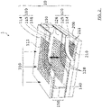
- the detector 1 comprises a first reflector 110 and a second reflector 120. These two reflectors 110, 120 are at a distance from each other so as to define a space forming a channel 140 for the circulation of a fluid possibly containing particles.
- the structural elements making it possible to keep the two reflectors 110,120 at a distance are not illustrated in this block diagram. These elements are for example pillars which leave free large openings allowing the fluid to flow into the channel 140. For example, one can provide pillars arranged in planes parallel to that of the sheet. These structural elements appear in picture 2 where they bear the reference number 150.
- Detector 1 is coupled to an optical source 300 and to an illumination system configured to bring light radiation 310 from source 300 to channel 140.
- the source is preferably separate from the detector. This makes it possible to change or manufacture the source independently of the detector.
- the source can for example be a laser, an LED or even the sun.
- the detector 1 is configured to form a resonant optical cavity 100 delimited by the first 110 and second 120 reflectors.
- the source 300 is chosen so that it feeds a cavity mode 10 at a precise wavelength as a function in particular of the spacing between the two reflectors 110, 120 and of their reflectivity spectrum.
- the operating wavelength or wavelengths are in the visible (380 to 780 nm) or near infrared (780 nm to 3 ⁇ m) spectral range, which makes it possible to greatly limit the costs of the detector 1.
- source 300 is a light-emitting diode LED or a laser.
- the first reflector 110 is for example a reflector based on Bragg mirrors.
- the second reflector 120 is a reflector based on membrane photonic crystals (PCM).
- the first reflector 110 can also be PCM-based.
- the first 110 and the second reflector 120 each extend along a plane. In the examples shown in figures 1A and 1B , this plane is perpendicular to that of the sheet. They are therefore planar reflectors.
- the reflectors are not planar. They can be curved. This may for example be the case if the reflectors are suspended. Furthermore, it may be useful to bend the reflectors, by applying stresses, in order to have an optically more stable cavity. Although curved, the first 110 and second 120 reflectors may be parallel.
- the first reflector 110 and the second reflector 120 together form a vertical resonant cavity 100. If the first 110 and second 120 reflectors are planar, the cavity mode 10 has an incidence perpendicular to the main plane in which the first 110 and second 120 reflectors extend. On the figures 1A and 1B , this mode of cavity 10 is therefore vertical.
- Detector 1 also includes a detection system 200.
- This detection system 200 includes for example an array of photodetectors 211 such as a matrix of photodiodes.
- the matrix can be linear or two-dimensional.
- the detector 1 is arranged so that part of the luminous flux brought into the cavity 100 escapes from the latter through the second reflector 120 and reaches the detection system 200.
- the photodetectors 211 and the channel 140 are arranged on either side of the second reflector 120. More specifically, the second reflector 120 has an internal face 122 facing the channel 140 and an external face 121 opposite the internal face 122.
- the second reflector 120 being placed between the cavity 100 and the detection system 200, it prevents the latter from being dazzled by the luminous flux present in the channel 140.
- the second reflector 120 induces radiation or leaks which escape from the cavity 100.
- this reflector 120 has a "radiation" pattern, also referred to as a “leakage” pattern 20, which is characteristic of the resonant mode of cavity 10.
- the analysis of the variations of the leakage diagram makes it possible to identify with great sensitivity a disturbance of the mode of cavity 10 and consequently to detect the presence of a disturber at the within channel 140.
- the Figure 1A represents the detector 1 in the absence of a particle within the channel 140.
- the luminous flux 310 generates an excited mode 10 centered on the point ⁇ of the reciprocal space of the second reflector 120 at PCM, that is to say in normal impact on the example shown.
- a mode excited at the point ⁇ of the reciprocal space of the second reflector 120 is called a “mode ⁇ ”.
- the detection system 200 In the absence of a particle, the detection system 200 therefore receives the leak diagram 20 specific to the mode ⁇ of cavity 10.
- the figure 1B represents the detector 1 in the presence of a particle 60 within the channel 140.
- This particle 60 disturbs the cavity mode.
- the ⁇ 10' mode is attenuated and non-vertical 10′′ diffractive modes appear.
- This disturbance of the cavity mode modifies the leakage diagram 20′.
- This modification of the leakage diagram 20′ can be read at the level of the detection system 200. This modification is characteristic of the nature of the disturber. It therefore makes it possible to identify the particle or particles 60 present in the cavity.
- This detector 1 comprises a cavity 100 and a detection system 200 configured to detect the leak diagram generated by the cavity 100.
- the cavity 100 comprises a first reflector 110, a second reflector 120 arranged at a distance from the first reflector 110 to create a free space forming a channel 140 for the circulation of the particles.
- the detector 1 comprises a single cavity 100 defining a single channel intended to receive a fluid transporting particles.
- Pillars 150 keep the first 110 and the second 120 reflectors at a distance.
- Detector 1 is coupled to an illumination system making it possible to generate light radiation.
- the lighting system brings the light radiation 310 to an outer face 111 of the first reflector 110, so that the light radiation passes through the first reflector 110 to reach the cavity 100.
- the photonic crystal membrane 115, 125 acts as a reflector.
- the photonic crystals 128 are planar, periodic patterns of a dielectric material. These patterns have a one-dimensional or two-dimensional periodicity.
- the figure 2 illustrates an example in which the patterns are one-dimensional. They can for example form a hole through the membrane 125. They can also be formed from a volume of material, for example a stud surrounded by a matrix. They can also form perfectly arbitrary and periodic patterns.
- each pattern 128 forming a bar extending along a main direction.
- the patterns 128 of the PCM-based reflectors 110, 120 can be arranged according to any type of mesh.
- the pattern (its size, shape and arrangement), the period of the array of patterns 128, the thickness and the refractive index of the membrane define the reflectivity spectrum of the PCM-based reflector. Ideally the reflectivity is maximum in the visible and near infrared spectral range.
- the encapsulation layers make it possible to bury the patterns.
- they are planarized. This allows the PCM-based reflector to have flat faces. This limits the deposits and the retention of particles on the internal faces 112, 122 of the reflectors 110, 120. Thus, the fouling of the detector is avoided and its reliability preserved over time.
- the reflectors 110,120 occupy, in the planes in which they mainly extend, a surface ranging from a few micrometers to a few square millimeters.
- the channel 140 is an area in which particles can circulate.
- the two reflectors 110,120 are spaced apart by pillars 150 or any structure that allows this function to be performed.
- the first 110 and the second 120 reflectors are separated by at least one different material which is not a part based on PCM membrane photonic crystals such as a reflector based on PCM for example. If it is desired to free the circulation of the particles as much as possible in planes parallel to those in which the reflectors 110,120 mainly extend, the section of the pillars 150 can be reduced.
- This solution aims to improve the fluidic response time of the detector 1
- This embodiment is particularly advantageous when the circulation of the fluid in the channel 140 is free, that is to say it is not forced. Furthermore, larger openings make the detector 1 less sensitive to fouling of the air zone.
- the pillars 150 can be structured so as to form a directional fluidic channel 140.
- This zone has a thickness of between a few micrometers and a few millimeters.
- the channel is through. It allows a flow of fluid between the first and second reflectors 110, 120 and inside the cavity 100.
- the channel 140 can be located entirely between the first 110 and second 120 reflectors.
- the channel 140 is configured so as to channel a flow of air which crosses the cavity 100 by flowing between the first 110 and second 120 reflectors, more precisely along the first 110 and second 120 reflectors.
- the channel 140 is configured so that the air flow passes through the cavity 100 by flowing in contact with the internal face 112 of the first reflector 110 and the internal face 122 of the second reflector 120.
- the detection system 200 is an assembly of at least one photodetector 211.
- the detection system 200 forms an array 210 of photodetectors 211 as illustrated in picture 2 .
- this is a pixel array or photodiode imager.
- the detector 1 comprises an optical device, such as a lens, located between the second reflector 120 and the array 210 of photodetectors 211 and configured so as to produce the image of mode 10 of cavity, disturbed or not, in the reciprocal space of the second reflector 120. This makes it possible to further refine the analysis of the disturber.
- an optical device such as a lens
- the lighting system brings the light radiation 310 onto the outer face 111 of the first reflector 110, so that the light radiation passes through the first reflector 110 to reach the cavity 100.
- the first reflector 110 preferably its internal face 112 is directly in contact with the pillars 150.
- the second reflector 120 preferably its internal face 122, is directly in contact with the pillars 150.
- the second reflector 120 and more particularly its outer face 121 is directly in contact with the detection system.
- the figures 3 to 5 illustrate different embodiments of the lighting system.
- the first reflector 110 may be a PCM-based reflector, a Bragg mirror reflector or any other type of reflector.
- the second reflector 120 is represented as a periodic arrangement of patterns 128 in the form of bars, any other type of pattern can be envisaged.
- the embodiment illustrated in picture 3 provides a lighting system similar to that of the figure 2 .
- the resonant cavity 100 mode 10 is powered by lighting from above, through the first reflector 110.
- the light radiation 310 is brought by the lighting system onto the external face 111 of the first reflector 110 and passes through this first reflector 110 to reach the interior of cavity 100.
- the figure 4 illustrates an embodiment in which the cavity 100 is supplied from an outer face 121 of the second reflector 120, this outer face 121 being opposite inside the cavity 100.
- the second reflector 120 being vertically located below the first reflector 110, it can be considered that the lighting takes place “from below”.
- An injection waveguide 311 is then provided, optically coupled to the source 300, which brings the light radiation 310 to the second reflector 120.
- the injection waveguide 311 excites the PCM-based reflector 120 by evanescent wave coupling.
- the first reflector 110 is also based on PCM. In this case, provision can be made for it to be the first reflector 110 and not the second reflector 120 which is coupled to the injection waveguide 311 to be excited by evanescent wave coupling.
- the injection waveguide 311 is produced by conventional microelectronics techniques, in particular by etching technique, typically of etching of thin layers such as for example a thin layer of silicon.
- etching technique typically of etching of thin layers such as for example a thin layer of silicon.
- this embodiment makes it possible to considerably reduce the bulk of the detector 1.
- the PCM-based reflector and the injection waveguide 311 are located on two different levels. These two elements can therefore have different thicknesses and/or be made of different materials, which makes it possible to relax the manufacturing constraints.
- the membrane can for example be made of silicon, of SIN nitride, of TIO2.
- the figure 5 illustrates an embodiment in which the cavity 100 is supplied by injecting the light radiation into the slice 129 of the membrane carrying the patterns 128 based on PCM 120.
- an injection waveguide 311 can be provided , optically coupled with a source 300, which has a portion 312 comprised in at least one plane identical to one of the planes in which the patterns 128 of the PCM-based reflector 120 mainly extend.
- the shape of this portion 312 is adapted to inject the light radiation along at least half, and preferably all, the dimension of the edge 129 of at least one of the patterns 128.
- the portion 312 widens in the direction of at least one pattern 128 to allow the light radiation 310 to penetrate the entire length of the edge 129 of this pattern 128.
- the portion 312 forms what is called a "taper in English.
- the first reflector 110 is also based on PCM. In this case, provision can be made for it to be the first reflector 110 and not not the second reflector 120 which is coupled to the injection waveguide 311 to be fed by the edge.
- This embodiment has the same advantages as the previous embodiment, in terms of simplicity of integration, in particular by conventional microelectronics techniques. Furthermore, this embodiment makes it possible to further reduce the size in the direction perpendicular to the planes in which the reflectors 110, 120 mainly extend.
- excitation modes described in figure 3 , 4 and 5 can of course be applied for patterns 128 other than bars and other than one-dimensional patterns.
- the source 300 is for example an LED or a LASER, this source must be able to supply a cavity mode 10 at a precise wavelength defined by the spacing between the two reflectors 110, 120 and by their reflectivity spectrum. This spacing is chosen in particular to allow the appearance of constructive interference.
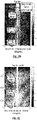
- the figure 6 is an example of a detector according to the invention simulated with the two-dimensional FDTD method (finite difference method in the time domain).
- the simulated detector 1 is an optical cavity 100 comprising two reflectors spaced apart by 15 ⁇ m.
- the X-axis Z is in micrometers.
- this first reflector 110 is formed of a Bragg mirror consisting of three alternations of thin layers of silica and amorphous silicon.
- the cavity 100 is illuminated through the first Bragg mirror reflector 110 by a plane wave which propagates along the Z axis.
- This plane wave has a wavelength around 850 nm, more precisely the wavelength closer to 850 nm which verifies the constructive interference condition.
- Detector 200 is placed behind PCM-based reflector 120.
- the detector 200 spatially measures the leaks from the cavity 100 disturbed by the presence of the particle 60.
- the figure 6 illustrates the power disturbance (Poynting vector). We would obtain a very similar visual by illustrating the disturbance of the Ey field. It is noted from this simulation that the cavity mode 10′ is disturbed and that diffractive modes 10′′ appear in the channel 140. Furthermore, it is noted that the leakage diagram is also disturbed 20′.
- the nature of the particle 60 in particular its size, can be determined by measuring the diagram of leaks from this cavity 100.
- 7A gives the radiation pattern in one dimension of the perturbed cavity 100 in the far field for particle diameters which vary from 50 nm to 0.9 ⁇ m.
- the figures 7A to 7C clearly illustrate the advantages offered by the invention in terms of sensitivity, in particular for detecting and analyzing particles of small size.
- the Figure 7A illustrates the leak diagram for a detector according to the example shown in figure 6 .
- This simulation shows that the detection system 200 collects numerous and precise angular information.
- the leaks of gallery modes 0, 1 and 2 appear clearly as illustrated by the references 61, 62, 63.
- the detection system 200 collects a strong signal for all the particles, including for the particles whose the size is less, or even very less than 500 nm, for example those less than 100 nm.
- This simulation also shows low glare for angles of zero or close to 0°.
- the figure 7B is a simulation illustrating the radiation pattern for a detector, not forming part of the invention, having a cavity formed by an upper reflector and a lower reflector, each of these two reflectors being a Bragg mirror,
- the two reflectors are identical and are each formed of three alternations of a-Si/SiO2, a-Si meaning amorphous silicon.
- the simulation shows that the angular information is poor. We find almost no leaks of gallery modes. In addition, the signal is weak for wide angles. However, the angular information is particularly important for accurately identifying the size of the particles. Low angular information in particular does not make it possible to identify whether a disturbance is due to a single particle of large size or to several small particles. It is clear from these simulations that the detector according to the invention makes it possible to significantly improve the sensitivity of detection compared to detectors based on resonant cavities, both of which are formed of Bragg mirrors.
- the Fig. 7C is a simulation illustrating the radiation diagram for a second reference detector not forming part of the invention and not comprising a cavity, the diffusion of the particle taking place directly on the array of photodetectors. We observe at the angle 0° a glare of the incident plane wave and a scattering diagram typical of a Mie scattering.
- Such a detector offers only a very weak signal for particles of small size, in particular those whose size is less than 500 nm.
- a detector according to the invention offers a significant gain in sensitivity compared with a conventional detector without a cavity.
- the figures 8A to 8F illustrate the main steps of a first example of a method for producing a detector according to the invention.
- a detection system 200 comprises for example an array 210 of photodiodes 211, such as a matrix of silicon photodiodes.
- the detection system 200 is in the form of a wafer also referred to as a plate.
- the detection system 200 is covered with a passivation layer, also referred to as encapsulation layer 124. This layer 124 is for example made of silica.
- a thin layer is then deposited which is structured to form the membrane 125 with photonic crystals 128.
- the membrane 125 with photonic crystals 128 is for example made from crystalline silicon, amorphous silicon, silicon nitride, titanium oxide or else another transparent material in the useful spectral range.
- This membrane 125 is then encapsulated by a passivation layer, also referred to as encapsulation layer 126.
- the face 122 that remains free of this passivation layer 126 is preferably planarized. This makes it possible to optically optimize the cavity and to limit the fouling of the detector.
- This encapsulation layer 126 is for example made of silica. It preferably has a low optical index compared to that of the membrane 125.
- the membrane 125 with photonic crystals 128 is thus encapsulated between the layers 124 and 126.
- the stack formed by the encapsulation layer 124, the membrane 125 and the encapsulation layer 126 forms the PCM-based reflector 120.
- a sacrificial layer 151 is then deposited on the encapsulation layer 126, for example with a photosensitive material.
- This material is for example a photosensitive resin which can be deposited for example with a spin coater.
- the thickness of this layer is preferably equal to the thickness of the air zone defined by channel 140 of detector 1.
- the figure 8D illustrates the formation of the pillars 150. These pillars are obtained by structuring the sacrificial layer 151. 151. Zone 152 is not removed at this stage and sacrificial layer 151 is then not etched during this step.
- the figure 8E illustrates the formation of the first reflector 110.
- this first reflector 110 is a Bragg mirror.
- the stack of layers of the Bragg mirror is deposited on the face that remains free of the sacrificial layer 151.
- the stack of layers of the Bragg mirror is deposited. It may for example be a periodic alternation of two layers of dielectric materials. These layers can be made of silica, crystalline silicon, amorphous silicon, silicon nitride, titanium oxide or another material that is transparent in the useful spectral range.
- the first The reflector 110 can be made up of a PCM-based reflector, which is structured or which is added above the sacrificial layer 151.
- the zone 152 is removed, which makes it possible to define the channel 140 allowing the passage of the fluid between the pillars 150.
- the stack thus produced constitutes at least part of the detector 1.
- the sacrificial layer 151 is formed on the first reflector 110 and not on the second reflector 120.
- the sacrificial layer 151 is etched before assembly of the upper reflector 110.
- the upper reflector 110 is then transferred onto the sacrificial layer 151, for example with a support substrate.
- FIG. 8F The embodiment described in figures 8 to 8F has the advantage of being simple, easily reproducible and inexpensive. It is particularly well suited to detectors whose channel 140 has a relatively small thickness, the thickness being taken in a direction perpendicular to the main plane in which the reflectors 110, 120 and the imager extend.
- the figures 9A to 9F illustrate the main steps of a second example of a method for producing a detector according to the invention.
- This method is particularly well suited to the production of detectors whose channel 140 has a high thickness, for example from 50 ⁇ m to 1 mm.
- a preferred application may for example be low consumption systems, which operate without a fluidic pump and by natural convection.
- the first steps can be similar to steps 7A and 7B of the method described above.
- a stack comprising a detection system 200 and a PCM-based reflector 120 is provided.
- a spacer forming at least one pillar 150 is carried out previously, in parallel or subsequently.
- the spacer is preferably the size of a wafer.
- This spacer forming the pillars 150 can for example be manufactured by printing in three dimensions (3D) or else by molding.
- the material used for the pillars 150 advantageously has a low coefficient of thermal expansion so as to have a cavity 100 that is optically stable under critical conditions, for example during a fire.
- the height of the spacer forming the pillars 150 corresponds to the thickness of the channel 140.
- this connecting portion 151 preferably extends only around the periphery of the cavity to be formed.
- the connecting portion 151 provides an opening in its center for the passage of light and does not mask the reflectors.
- the connecting portion 151 forms a frame for connecting the spacers 150. This frame corresponds to the periphery of the reflectors 110, 120. It will be polygonal if the reflectors 110, 120 are polygonal and will be circular if the reflectors 110, 120 each form a disk.
- the first reflector 110 As illustrated in figure 9C , one carries out, previously, in parallel or after the steps illustrated in figures 9A and 9B , the first reflector 110.
- the first reflector 110 is formed from another support substrate 130, for example made of silicon.
- the first reflector 110 can be a Bragg mirror or a PCM-based reflector.
- the figure 9D illustrates the reversal of the stack incorporating the first reflector 110.
- a deep etching of the substrate 130 is then carried out until the first reflector 110 is reached, that is to say the stack of layers of the Bragg mirror in this example.
- This opening of the substrate 130 makes it possible to illuminate the cavity 100 through the first reflector 110.
- a closed periphery or pads 132 are kept on the periphery of the substrate 130.
- the substrate 130 is transparent in the useful wavelength range, for example if the substrate is glass, then this deep etching step shown in Figure 9E is not necessary.
- the stacks produced separately are assembled together. These assemblies are made for example with optical glue.
- the stack comprising the first reflector 110 and the stack comprising the second reflector 120 are arranged on either side of the spacer forming the pillars 150.
- a variant of this method consists in replacing the spacer forming the pillars 150 by structuring the substrate 130.
- a very thick substrate 132 is provided, typically, the thickness of which corresponds to the desired height of the pillars 150 and the channel 140.
- the spacer forming the pillars 150 and the first reflector 110 then belong to the same part and are returned to be assembled with the stack comprising the PCM-based reflector 120.
- the thickness of the air zone is limited by the thickness of the substrate 130, the thickness of which is for example 725 ⁇ m.
- a system comprising two resonant cavities 100,100' is provided.
- One of the two cavities 100, 100' is open so that a fluid enters the channel 140 to bring any particles therein.
- the other cavity 100' is sealed and free of particles. It thus constitutes a reference cavity.
- the space 140' of the cavity 100' is thus entirely delimited by the first 110 and second 120 reflectors and by a continuous wall forming a closed contour to define a closed space.
- each cavity 100, 100' is associated with an illumination system 310 which preferably shares the same source 300, a first reflector 110, a reflector 120 based on PCM and a detection system 200.
- this system comprises two detectors 1, 1' in accordance with the above descriptions, with the difference that one of the two detectors 1, 1' has a cavity 100' isolated from the particles to form a reference cavity. Provision can be made for the detection systems 200 of each of these detectors to be coupled. The signals from these two detectors are then analyzed by a processing unit 11 of the system.
- a detector having a sealed reference cavity can be made in various ways. It can be made using the process illustrated in figure 9A to 9F . Using the process illustrated in figures 8A to 8F , the sacrificial layer 151 should be etched before assembly of the first 110 and second reflector 120. For this, one of the two reflectors 110, 120 can be transferred to the channel already etched, this reflector then being carried by a support substrate.
- the invention proposes an effective solution for improving the sensitivity and precision of the detector, in particular for detecting particles of very small size, typically particles whose size is less than 500 nm or even less than 250 nm.
- an optical system such as a lens between the PCM-based reflector 120 and the detection system 200, typically a matrix of photodetectors, so as to produce the image of the cavity mode. in the reciprocal space of the PCM-based reflector 120.
- This solution makes it possible to further refine the analysis of the disturber present in the cavity 100.
Landscapes
- Physics & Mathematics (AREA)
- Chemical & Material Sciences (AREA)
- General Physics & Mathematics (AREA)
- Optics & Photonics (AREA)
- Biochemistry (AREA)
- Analytical Chemistry (AREA)
- Life Sciences & Earth Sciences (AREA)
- General Health & Medical Sciences (AREA)
- Health & Medical Sciences (AREA)
- Immunology (AREA)
- Pathology (AREA)
- Dispersion Chemistry (AREA)
- Crystallography & Structural Chemistry (AREA)
- Investigating Or Analysing Materials By Optical Means (AREA)
Claims (15)
- Detektor (1) von Partikeln (60), mindestens umfassend:- mindestens einen Hohlraumresonator (100), mindestens teilweise durch einen ersten Reflektor (110) gebildet, einen zweiten Reflektor (120), in einem Abstand vom ersten Reflektor (110) angeordnet, und einen Kanal (140), der zwischen dem ersten (110) und dem zweiten (120) Reflektor liegt, wobei der Kanal (140) bestimmt ist, um mindestens ein Fluid zu empfangen, Partikel (60) umfassend, und mindestens eine Lichtstrahlung (310) zu empfangen;- mindestens ein Detektionssystem (200), mindestens einen Photodetektor (211) umfassend,- dadurch gekennzeichnet, dass der Detektor (1) so konfiguriert ist, dass ein Teil der im Kanal (140) vorhandenen Lichtstrahlung aus dem Hohlraum (100) entweicht, indem sie den zweiten Reflektor (120) durchläuft und zum Detektionssystem (200) gelangt, wodurch der mindestens eine Photodetektor (211) Lecks (20) im Hohlraum (100) erkennen kann,- und dass der zweite Reflektor (120) ein Reflektor ist, der auf photonischen Kristallmembranen PCM basiert.
- Detektor (1) nach dem vorhergehenden Anspruch, wobei der erste Reflektor (110) und der zweite Reflektor (120) einander zugewandt angeordnet sind, sich in zwei parallelen Ebenen erstreckend und konfiguriert, um einen optischen Hohlraumresonator (100) zu bilden, der einen Hohlraummode (10) senkrecht zu den Ebenen aufweist, in denen sich grundsätzlich der erste Reflektor (110) und der zweite Reflektor (120) erstrecken.
- Detektor (1) nach einem der vorhergehenden Ansprüche, wobei das Detektionssystem (200) eine Anordnung (210) von Photodetektoren (211) beinhaltet, die in Form einer Photodetektorenmatrix eingerichtet sind.
- Detektor (1) nach einem der vorhergehenden Ansprüche, wobei der erste Reflektor (110) mindestens einen Bragg-Spiegel umfasst oder daraus besteht.
- Detektor (1) nach einem der Ansprüche 1 bis 3, wobei der erste Reflektor (110) ein Reflektor ist, der auf photonischen Kristallmembranen PCM basiert.
- Detektor (1) nach einem der vorhergehenden Ansprüche, wobei der zweite PCM-basierte Reflektor (120) Muster (128) aufweist, die aus einem dielektrischen Material gebildet und periodisch angeordnet sind, wobei mindestens eines der Merkmale des zweiten Reflektors (120) insbesondere aus der Größe der Muster (128), der Form der Muster (128), der Periode der Muster (128), der Dicke der Muster und dem Brechungsindex des zweiten Reflektors (120) so ausgewählt sind, dass die maximale Reflektivität des zweiten Reflektors (120) einer Wellenlänge entspricht, die zum Bereich des sichtbaren Spektrums (380 bis 780 nm) oder des Nahinfrarots (780 nm bis 3µm) gehört.
- Detektor (1) nach einem der vorhergehenden Ansprüche, wobei der zweite PCM-basierte Reflektor (120) Muster (128) umfasst, die aus einem dielektrischen Material gebildet sind, und mindestens eine Verkapselungsschicht (126), die die Muster (128) bedeckt und eine ebene Fläche (122) aufweist, wobei die mindestens eine Verkapselungsschicht (126) vorzugsweise aus einem dielektrischen Material besteht.
- Detektor (1) nach einem der vorhergehenden Ansprüche, mindestens ein Beleuchtungssystem umfassend, konfiguriert, um mindestens eine Lichtstrahlung (310) in den Hohlraum (100) zu bringen.
- Detektor (1) nach dem vorhergehenden Anspruch, wobei:- das Beleuchtungssystem konfiguriert ist, um die mindestens eine Lichtstrahlung (310) in den Kanal (140) zu bringen, indem sie den ersten Reflektor (110) durchläuft,- oder der zweite Reflektor (120) eine dem Kanal (140) zugewandte Innenfläche (122) aufweist und eine der Innenfläche (122) gegenüberliegende Außenfläche (121), und das Beleuchtungssystem einen Injektionswellenleiter (311) umfasst, konfiguriert, um den Lichtstrom (310) auf die Außenfläche (121) zu bringen, um den zweiten Reflektor (120) durch Kopplung von evaneszenten Wellen zu erregen,- oder der erste Reflektor (110) PCM-basiert ist und eine dem Kanal (140) zugewandte Innenfläche (112) aufweist und eine der Innenfläche (112) gegenüberliegende Außenfläche (111), und das Beleuchtungssystem einen Injektionswellenleiter umfasst, konfiguriert, um den Lichtstrom auf die Außenfläche (111) zu bringen, um den ersten Reflektor (110) durch Kopplung von evaneszenten Wellen zu erregen,- oder der zweite PCM-basierte Reflektor (120) einen Wafer (129) aufweist, und das Beleuchtungssystem einen Injektionswellenleiter (311) umfasst, konfiguriert, um die Lichtstrahlung (311) bis zum Wafer (129) des zweiten PCM-basierten Reflektors (120) zu leiten,- oder der erste Reflektor (110) PCM-basiert ist und einen Wafer aufweist, und das Beleuchtungssystem einen Injektionswellenleiter umfasst, konfiguriert, um die Lichtstrahlung bis zum Wafer des ersten PCM-basierten Reflektors (110) zu leiten.
- Detektor (1) nach einem der vorhergehenden Ansprüche, eine Lichtquelle (300) umfassend, die optisch mit dem Beleuchtungssystem gekoppelt ist, wobei die Quelle (300) ein Laser oder eine Leuchtdiode LED ist.
- Detektor (1) nach einem der vorhergehenden Ansprüche, eine optische Vorrichtung umfassend, beispielsweise eine Linse, die zwischen dem zweiten Reflektor (120) und dem Detektionssystem (200) angeordnet ist, wobei die optische Vorrichtung so konfiguriert ist, dass das Bild des Hohlraummode im Impulsraum des zweiten Reflektors (120) liegt.
- Detektionssystem, einen ersten Detektor (1) nach einem der vorhergehenden Ansprüche umfassend und einen zweiten Detektor (1') nach einem der vorhergehenden Ansprüche, wobei ein Hohlraum (100') des zweiten Detektors (1'), Referenzhohlraum genannt, abgedichtet ist, um zu verhindern, dass Partikel in den Referenzhohlraum (100') eintreten, wobei das System ferner konfiguriert ist, um Daten, die vom Detektionssystem (200) des ersten Detektors (1) bereitgestellt werden, mit Daten zu koppeln, die vom Detektionssystem (200) des zweiten Detektors (1') bereitgestellt werden.
- System, mindestens einen Detektor (1) nach einem der Ansprüche 1 bis 11 umfassend, wobei das System ausgewählt wird aus:- einem Brandmeldesystem,- einem Branddetektionssystem,- einem Qualitätsanalysesystem eines Fluids wie Luft oder Wasser,- einem Emissionsminderungsmeldesystem,- einem Sprengpulverdetektionssystem,- einem Detektionssystem von mikrobiologischen Spezies.
- Herstellungsverfahren eines Partikeldetektors (60) nach einem der Ansprüche 1 bis 11, wobei das Verfahren mindestens die folgenden Schritte umfasst:- Bereitstellen mindestens eines Stapels, einen ersten Reflektor (110) umfassend,- Bereitstellen mindestens eines Stapels, einen zweiten Reflektor (120) umfassend, wobei der zweite Reflektor (120) auf PCM-basierend ist,- Herstellen von Säulen (150),- Zusammenbauen des ersten Reflektors (110) und des zweiten Reflektors (120), so dass der erste Reflektor (110) und der zweite Reflektor (120) auf beiden Seiten der Säulen (150) zu liegen kommen, um zwischen den Säulen (150) einen Kanal (140) für den Durchlass des Fluids zu erhalten.
- Verfahren nach dem vorhergehenden Anspruch, mindestens die folgenden Schritte umfassend:- vor dem Zusammenbau des ersten Reflektors (110) und des zweiten Reflektors (120) wird eine Opferschicht (151) auf dem ersten Reflektor (110) oder dem zweiten Reflektor (120) bereitstellt,- vor oder nach dem Zusammenbau des ersten Reflektors (110) und des zweiten Reflektors (120) wird ein Teil (152) der Opferschicht (151) entfernt, unter Beibehaltung eines weiteren Teils der Opferschicht (151), um die Säulen (150) und den Kanal (140) zu bilden.
Applications Claiming Priority (2)
| Application Number | Priority Date | Filing Date | Title |
|---|---|---|---|
| FR1874037A FR3090873B1 (fr) | 2018-12-21 | 2018-12-21 | Détecteur optique de particules |
| PCT/EP2019/086982 WO2020128105A1 (fr) | 2018-12-21 | 2019-12-23 | Détecteur optique de particules |
Publications (2)
| Publication Number | Publication Date |
|---|---|
| EP3899490A1 EP3899490A1 (de) | 2021-10-27 |
| EP3899490B1 true EP3899490B1 (de) | 2022-11-16 |
Family
ID=67660157
Family Applications (1)
| Application Number | Title | Priority Date | Filing Date |
|---|---|---|---|
| EP19824370.1A Active EP3899490B1 (de) | 2018-12-21 | 2019-12-23 | Vorrichtung zur optischen partikeldetektion |
Country Status (4)
| Country | Link |
|---|---|
| US (1) | US20220146402A1 (de) |
| EP (1) | EP3899490B1 (de) |
| FR (1) | FR3090873B1 (de) |
| WO (1) | WO2020128105A1 (de) |
Families Citing this family (1)
| Publication number | Priority date | Publication date | Assignee | Title |
|---|---|---|---|---|
| EP3839479B1 (de) * | 2019-12-20 | 2024-04-03 | IMEC vzw | Vorrichtung zum nachweis von partikeln in der luft |
Family Cites Families (6)
| Publication number | Priority date | Publication date | Assignee | Title |
|---|---|---|---|---|
| FR2963101B1 (fr) | 2010-07-22 | 2013-02-15 | Commissariat Energie Atomique | Detecteur de particules et procede de realisation d'un tel detecteur |
| EP2625556A2 (de) * | 2010-10-08 | 2013-08-14 | Cornell University | Vorrichtung, verfahren und anwendungen mit photonenkristallresonatoren für optische erfassung |
| WO2012099848A1 (en) * | 2011-01-18 | 2012-07-26 | The Regents Of The University Of Michigan | Fabry-perot based optofluidic sensor |
| US10132934B2 (en) | 2014-09-17 | 2018-11-20 | Stmicroelectronics S.R.L. | Integrated detection device, in particular detector of particles such as particulates or alpha particles |
| GB201609017D0 (en) * | 2016-05-23 | 2016-07-06 | Isis Innovation | Characterisation of particles |
| FR3063147B1 (fr) | 2017-02-20 | 2023-08-25 | Commissariat Energie Atomique | Detecteur optique de particules |
-
2018
- 2018-12-21 FR FR1874037A patent/FR3090873B1/fr active Active
-
2019
- 2019-12-23 EP EP19824370.1A patent/EP3899490B1/de active Active
- 2019-12-23 US US17/416,268 patent/US20220146402A1/en active Pending
- 2019-12-23 WO PCT/EP2019/086982 patent/WO2020128105A1/fr unknown
Also Published As
| Publication number | Publication date |
|---|---|
| US20220146402A1 (en) | 2022-05-12 |
| EP3899490A1 (de) | 2021-10-27 |
| FR3090873A1 (fr) | 2020-06-26 |
| WO2020128105A1 (fr) | 2020-06-25 |
| FR3090873B1 (fr) | 2021-07-23 |
Similar Documents
| Publication | Publication Date | Title |
|---|---|---|
| EP2596329B1 (de) | Partikeldetektor und verfahren zur herstellung eines derartigen detektors | |
| WO2018138223A1 (fr) | Détecteur optique de particules | |
| EP3671179A1 (de) | Optischer teilchendetektor | |
| EP3899490B1 (de) | Vorrichtung zur optischen partikeldetektion | |
| EP3583402B1 (de) | Optischer partikeldetektor und verfahren zur herstellung eines optischen partikeldetektor | |
| EP3502750A1 (de) | Strukturierter plastikszintillator | |
| EP2710351B1 (de) | Biochip-vorrichtung | |
| FR2964469A1 (fr) | Substrat revetu de nanoparticules, et son utilisation pour la detection de molecules isolees. | |
| WO2017220919A1 (fr) | Reflecteur optique resonant a multiples couches minces de materiaux dielectriques, capteur optique, dispositif d'amplification laser comportant un tel reflecteur et procedes de fabrication correspondants | |
| EP3971550B1 (de) | Optischer teilchendetektor und herstellungsverfahren | |
| EP3436807A1 (de) | Verfahren und system zur inspektion von platten für die mikroelektronik oder optik durch laser-doppler-effekt | |
| EP2565623B1 (de) | Vorrichtung zur optischen Messung von Materialien anhand eines Multiplexverfahrens von Licht | |
| EP3598102A1 (de) | Optischer teilchendetektor | |
| EP2877836A1 (de) | Optisches verfahren zur beobachtung von proben und zum erfassen bzw. messen chemischer oder biologischer spezies | |
| EP3933379B1 (de) | Optischer teilchensensor | |
| EP2565627B1 (de) | Vorrichtung zur Beleuchtung eines Objekts mit einer Lichtquelle umfassend Mitteln zur Probeentnahme eines Lichtanteils um Variationen der Lichtquelleintensität zu messen. | |
| WO2021078805A1 (fr) | Détecteur optique de particules | |
| EP3968066A1 (de) | Wellenleiter, der eine optische multimode-faser umfasst und die geführten moden räumlich konzentrieren kann | |
| FR3027112A1 (fr) | Procede de caracterisation d'un champ electromagnetique genere par l'interaction d'une onde electromagnetique avec une structure photonique et/ou plasmonique | |
| FR3004814A1 (fr) | Systeme de detection optique comportant un dispositif de collection de lumiere | |
| FR3000810A1 (fr) | Guide d'onde, dispositif de captation de lumiere et procede de fabrication d'un guide d'onde |
Legal Events
| Date | Code | Title | Description |
|---|---|---|---|
| STAA | Information on the status of an ep patent application or granted ep patent |
Free format text: STATUS: UNKNOWN |
|
| STAA | Information on the status of an ep patent application or granted ep patent |
Free format text: STATUS: THE INTERNATIONAL PUBLICATION HAS BEEN MADE |
|
| PUAI | Public reference made under article 153(3) epc to a published international application that has entered the european phase |
Free format text: ORIGINAL CODE: 0009012 |
|
| STAA | Information on the status of an ep patent application or granted ep patent |
Free format text: STATUS: REQUEST FOR EXAMINATION WAS MADE |
|
| 17P | Request for examination filed |
Effective date: 20210708 |
|
| AK | Designated contracting states |
Kind code of ref document: A1 Designated state(s): AL AT BE BG CH CY CZ DE DK EE ES FI FR GB GR HR HU IE IS IT LI LT LU LV MC MK MT NL NO PL PT RO RS SE SI SK SM TR |
|
| DAV | Request for validation of the european patent (deleted) | ||
| DAX | Request for extension of the european patent (deleted) | ||
| GRAP | Despatch of communication of intention to grant a patent |
Free format text: ORIGINAL CODE: EPIDOSNIGR1 |
|
| STAA | Information on the status of an ep patent application or granted ep patent |
Free format text: STATUS: GRANT OF PATENT IS INTENDED |
|
| INTG | Intention to grant announced |
Effective date: 20220603 |
|
| GRAS | Grant fee paid |
Free format text: ORIGINAL CODE: EPIDOSNIGR3 |
|
| GRAA | (expected) grant |
Free format text: ORIGINAL CODE: 0009210 |
|
| STAA | Information on the status of an ep patent application or granted ep patent |
Free format text: STATUS: THE PATENT HAS BEEN GRANTED |
|
| AK | Designated contracting states |
Kind code of ref document: B1 Designated state(s): AL AT BE BG CH CY CZ DE DK EE ES FI FR GB GR HR HU IE IS IT LI LT LU LV MC MK MT NL NO PL PT RO RS SE SI SK SM TR |
|
| REG | Reference to a national code |
Ref country code: GB Ref legal event code: FG4D Free format text: NOT ENGLISH |
|
| REG | Reference to a national code |
Ref country code: CH Ref legal event code: EP |
|
| REG | Reference to a national code |
Ref country code: DE Ref legal event code: R096 Ref document number: 602019022065 Country of ref document: DE |
|
| REG | Reference to a national code |
Ref country code: IE Ref legal event code: FG4D Free format text: LANGUAGE OF EP DOCUMENT: FRENCH |
|
| REG | Reference to a national code |
Ref country code: AT Ref legal event code: REF Ref document number: 1532037 Country of ref document: AT Kind code of ref document: T Effective date: 20221215 |
|
| REG | Reference to a national code |
Ref country code: LT Ref legal event code: MG9D |
|
| REG | Reference to a national code |
Ref country code: NL Ref legal event code: MP Effective date: 20221116 |
|
| REG | Reference to a national code |
Ref country code: AT Ref legal event code: MK05 Ref document number: 1532037 Country of ref document: AT Kind code of ref document: T Effective date: 20221116 |
|
| PG25 | Lapsed in a contracting state [announced via postgrant information from national office to epo] |
Ref country code: SE Free format text: LAPSE BECAUSE OF FAILURE TO SUBMIT A TRANSLATION OF THE DESCRIPTION OR TO PAY THE FEE WITHIN THE PRESCRIBED TIME-LIMIT Effective date: 20221116 Ref country code: PT Free format text: LAPSE BECAUSE OF FAILURE TO SUBMIT A TRANSLATION OF THE DESCRIPTION OR TO PAY THE FEE WITHIN THE PRESCRIBED TIME-LIMIT Effective date: 20230316 Ref country code: NO Free format text: LAPSE BECAUSE OF FAILURE TO SUBMIT A TRANSLATION OF THE DESCRIPTION OR TO PAY THE FEE WITHIN THE PRESCRIBED TIME-LIMIT Effective date: 20230216 Ref country code: LT Free format text: LAPSE BECAUSE OF FAILURE TO SUBMIT A TRANSLATION OF THE DESCRIPTION OR TO PAY THE FEE WITHIN THE PRESCRIBED TIME-LIMIT Effective date: 20221116 Ref country code: FI Free format text: LAPSE BECAUSE OF FAILURE TO SUBMIT A TRANSLATION OF THE DESCRIPTION OR TO PAY THE FEE WITHIN THE PRESCRIBED TIME-LIMIT Effective date: 20221116 Ref country code: ES Free format text: LAPSE BECAUSE OF FAILURE TO SUBMIT A TRANSLATION OF THE DESCRIPTION OR TO PAY THE FEE WITHIN THE PRESCRIBED TIME-LIMIT Effective date: 20221116 Ref country code: AT Free format text: LAPSE BECAUSE OF FAILURE TO SUBMIT A TRANSLATION OF THE DESCRIPTION OR TO PAY THE FEE WITHIN THE PRESCRIBED TIME-LIMIT Effective date: 20221116 |
|
| PG25 | Lapsed in a contracting state [announced via postgrant information from national office to epo] |
Ref country code: RS Free format text: LAPSE BECAUSE OF FAILURE TO SUBMIT A TRANSLATION OF THE DESCRIPTION OR TO PAY THE FEE WITHIN THE PRESCRIBED TIME-LIMIT Effective date: 20221116 Ref country code: PL Free format text: LAPSE BECAUSE OF FAILURE TO SUBMIT A TRANSLATION OF THE DESCRIPTION OR TO PAY THE FEE WITHIN THE PRESCRIBED TIME-LIMIT Effective date: 20221116 Ref country code: LV Free format text: LAPSE BECAUSE OF FAILURE TO SUBMIT A TRANSLATION OF THE DESCRIPTION OR TO PAY THE FEE WITHIN THE PRESCRIBED TIME-LIMIT Effective date: 20221116 Ref country code: IS Free format text: LAPSE BECAUSE OF FAILURE TO SUBMIT A TRANSLATION OF THE DESCRIPTION OR TO PAY THE FEE WITHIN THE PRESCRIBED TIME-LIMIT Effective date: 20230316 Ref country code: HR Free format text: LAPSE BECAUSE OF FAILURE TO SUBMIT A TRANSLATION OF THE DESCRIPTION OR TO PAY THE FEE WITHIN THE PRESCRIBED TIME-LIMIT Effective date: 20221116 Ref country code: GR Free format text: LAPSE BECAUSE OF FAILURE TO SUBMIT A TRANSLATION OF THE DESCRIPTION OR TO PAY THE FEE WITHIN THE PRESCRIBED TIME-LIMIT Effective date: 20230217 |
|
| PG25 | Lapsed in a contracting state [announced via postgrant information from national office to epo] |
Ref country code: NL Free format text: LAPSE BECAUSE OF FAILURE TO SUBMIT A TRANSLATION OF THE DESCRIPTION OR TO PAY THE FEE WITHIN THE PRESCRIBED TIME-LIMIT Effective date: 20221116 |
|
| PG25 | Lapsed in a contracting state [announced via postgrant information from national office to epo] |
Ref country code: SM Free format text: LAPSE BECAUSE OF FAILURE TO SUBMIT A TRANSLATION OF THE DESCRIPTION OR TO PAY THE FEE WITHIN THE PRESCRIBED TIME-LIMIT Effective date: 20221116 Ref country code: RO Free format text: LAPSE BECAUSE OF FAILURE TO SUBMIT A TRANSLATION OF THE DESCRIPTION OR TO PAY THE FEE WITHIN THE PRESCRIBED TIME-LIMIT Effective date: 20221116 Ref country code: EE Free format text: LAPSE BECAUSE OF FAILURE TO SUBMIT A TRANSLATION OF THE DESCRIPTION OR TO PAY THE FEE WITHIN THE PRESCRIBED TIME-LIMIT Effective date: 20221116 Ref country code: DK Free format text: LAPSE BECAUSE OF FAILURE TO SUBMIT A TRANSLATION OF THE DESCRIPTION OR TO PAY THE FEE WITHIN THE PRESCRIBED TIME-LIMIT Effective date: 20221116 Ref country code: CZ Free format text: LAPSE BECAUSE OF FAILURE TO SUBMIT A TRANSLATION OF THE DESCRIPTION OR TO PAY THE FEE WITHIN THE PRESCRIBED TIME-LIMIT Effective date: 20221116 |
|
| REG | Reference to a national code |
Ref country code: CH Ref legal event code: PL |
|
| REG | Reference to a national code |
Ref country code: DE Ref legal event code: R097 Ref document number: 602019022065 Country of ref document: DE |
|
| REG | Reference to a national code |
Ref country code: BE Ref legal event code: MM Effective date: 20221231 |
|
| PG25 | Lapsed in a contracting state [announced via postgrant information from national office to epo] |
Ref country code: SK Free format text: LAPSE BECAUSE OF FAILURE TO SUBMIT A TRANSLATION OF THE DESCRIPTION OR TO PAY THE FEE WITHIN THE PRESCRIBED TIME-LIMIT Effective date: 20221116 Ref country code: LU Free format text: LAPSE BECAUSE OF NON-PAYMENT OF DUE FEES Effective date: 20221223 Ref country code: AL Free format text: LAPSE BECAUSE OF FAILURE TO SUBMIT A TRANSLATION OF THE DESCRIPTION OR TO PAY THE FEE WITHIN THE PRESCRIBED TIME-LIMIT Effective date: 20221116 |
|
| PLBE | No opposition filed within time limit |
Free format text: ORIGINAL CODE: 0009261 |
|
| STAA | Information on the status of an ep patent application or granted ep patent |
Free format text: STATUS: NO OPPOSITION FILED WITHIN TIME LIMIT |
|
| 26N | No opposition filed |
Effective date: 20230817 |
|
| PG25 | Lapsed in a contracting state [announced via postgrant information from national office to epo] |
Ref country code: LI Free format text: LAPSE BECAUSE OF NON-PAYMENT OF DUE FEES Effective date: 20221231 Ref country code: IE Free format text: LAPSE BECAUSE OF NON-PAYMENT OF DUE FEES Effective date: 20221223 Ref country code: CH Free format text: LAPSE BECAUSE OF NON-PAYMENT OF DUE FEES Effective date: 20221231 |
|
| PG25 | Lapsed in a contracting state [announced via postgrant information from national office to epo] |
Ref country code: SI Free format text: LAPSE BECAUSE OF FAILURE TO SUBMIT A TRANSLATION OF THE DESCRIPTION OR TO PAY THE FEE WITHIN THE PRESCRIBED TIME-LIMIT Effective date: 20221116 Ref country code: BE Free format text: LAPSE BECAUSE OF NON-PAYMENT OF DUE FEES Effective date: 20221231 |
|
| PGFP | Annual fee paid to national office [announced via postgrant information from national office to epo] |
Ref country code: GB Payment date: 20231221 Year of fee payment: 5 |
|
| PGFP | Annual fee paid to national office [announced via postgrant information from national office to epo] |
Ref country code: FR Payment date: 20231221 Year of fee payment: 5 Ref country code: DE Payment date: 20231219 Year of fee payment: 5 |
|
| PG25 | Lapsed in a contracting state [announced via postgrant information from national office to epo] |
Ref country code: CY Free format text: LAPSE BECAUSE OF FAILURE TO SUBMIT A TRANSLATION OF THE DESCRIPTION OR TO PAY THE FEE WITHIN THE PRESCRIBED TIME-LIMIT Effective date: 20221116 |