EP3896804A1 - Laser amplifier - Google Patents
Laser amplifier Download PDFInfo
- Publication number
- EP3896804A1 EP3896804A1 EP19909111.7A EP19909111A EP3896804A1 EP 3896804 A1 EP3896804 A1 EP 3896804A1 EP 19909111 A EP19909111 A EP 19909111A EP 3896804 A1 EP3896804 A1 EP 3896804A1
- Authority
- EP
- European Patent Office
- Prior art keywords
- light
- core layer
- input
- signal light
- laser amplifier
- Prior art date
- Legal status (The legal status is an assumption and is not a legal conclusion. Google has not performed a legal analysis and makes no representation as to the accuracy of the status listed.)
- Granted
Links
Images




Classifications
-
- G—PHYSICS
- G02—OPTICS
- G02B—OPTICAL ELEMENTS, SYSTEMS OR APPARATUS
- G02B27/00—Optical systems or apparatus not provided for by any of the groups G02B1/00 - G02B26/00, G02B30/00
- G02B27/09—Beam shaping, e.g. changing the cross-sectional area, not otherwise provided for
- G02B27/0938—Using specific optical elements
- G02B27/095—Refractive optical elements
- G02B27/0972—Prisms
-
- H—ELECTRICITY
- H01—ELECTRIC ELEMENTS
- H01S—DEVICES USING THE PROCESS OF LIGHT AMPLIFICATION BY STIMULATED EMISSION OF RADIATION [LASER] TO AMPLIFY OR GENERATE LIGHT; DEVICES USING STIMULATED EMISSION OF ELECTROMAGNETIC RADIATION IN WAVE RANGES OTHER THAN OPTICAL
- H01S3/00—Lasers, i.e. devices using stimulated emission of electromagnetic radiation in the infrared, visible or ultraviolet wave range
- H01S3/05—Construction or shape of optical resonators; Accommodation of active medium therein; Shape of active medium
- H01S3/06—Construction or shape of active medium
- H01S3/063—Waveguide lasers, i.e. whereby the dimensions of the waveguide are of the order of the light wavelength
-
- G—PHYSICS
- G02—OPTICS
- G02B—OPTICAL ELEMENTS, SYSTEMS OR APPARATUS
- G02B27/00—Optical systems or apparatus not provided for by any of the groups G02B1/00 - G02B26/00, G02B30/00
- G02B27/09—Beam shaping, e.g. changing the cross-sectional area, not otherwise provided for
- G02B27/0938—Using specific optical elements
- G02B27/095—Refractive optical elements
- G02B27/0955—Lenses
-
- G—PHYSICS
- G02—OPTICS
- G02B—OPTICAL ELEMENTS, SYSTEMS OR APPARATUS
- G02B6/00—Light guides; Structural details of arrangements comprising light guides and other optical elements, e.g. couplings
- G02B6/24—Coupling light guides
- G02B6/26—Optical coupling means
- G02B6/32—Optical coupling means having lens focusing means positioned between opposed fibre ends
-
- G—PHYSICS
- G02—OPTICS
- G02B—OPTICAL ELEMENTS, SYSTEMS OR APPARATUS
- G02B6/00—Light guides; Structural details of arrangements comprising light guides and other optical elements, e.g. couplings
- G02B6/24—Coupling light guides
- G02B6/42—Coupling light guides with opto-electronic elements
-
- H—ELECTRICITY
- H01—ELECTRIC ELEMENTS
- H01S—DEVICES USING THE PROCESS OF LIGHT AMPLIFICATION BY STIMULATED EMISSION OF RADIATION [LASER] TO AMPLIFY OR GENERATE LIGHT; DEVICES USING STIMULATED EMISSION OF ELECTROMAGNETIC RADIATION IN WAVE RANGES OTHER THAN OPTICAL
- H01S3/00—Lasers, i.e. devices using stimulated emission of electromagnetic radiation in the infrared, visible or ultraviolet wave range
- H01S3/005—Optical devices external to the laser cavity, specially adapted for lasers, e.g. for homogenisation of the beam or for manipulating laser pulses, e.g. pulse shaping
-
- H—ELECTRICITY
- H01—ELECTRIC ELEMENTS
- H01S—DEVICES USING THE PROCESS OF LIGHT AMPLIFICATION BY STIMULATED EMISSION OF RADIATION [LASER] TO AMPLIFY OR GENERATE LIGHT; DEVICES USING STIMULATED EMISSION OF ELECTROMAGNETIC RADIATION IN WAVE RANGES OTHER THAN OPTICAL
- H01S3/00—Lasers, i.e. devices using stimulated emission of electromagnetic radiation in the infrared, visible or ultraviolet wave range
- H01S3/05—Construction or shape of optical resonators; Accommodation of active medium therein; Shape of active medium
- H01S3/06—Construction or shape of active medium
- H01S3/063—Waveguide lasers, i.e. whereby the dimensions of the waveguide are of the order of the light wavelength
- H01S3/0632—Thin film lasers in which light propagates in the plane of the thin film
-
- H—ELECTRICITY
- H01—ELECTRIC ELEMENTS
- H01S—DEVICES USING THE PROCESS OF LIGHT AMPLIFICATION BY STIMULATED EMISSION OF RADIATION [LASER] TO AMPLIFY OR GENERATE LIGHT; DEVICES USING STIMULATED EMISSION OF ELECTROMAGNETIC RADIATION IN WAVE RANGES OTHER THAN OPTICAL
- H01S3/00—Lasers, i.e. devices using stimulated emission of electromagnetic radiation in the infrared, visible or ultraviolet wave range
- H01S3/05—Construction or shape of optical resonators; Accommodation of active medium therein; Shape of active medium
- H01S3/08—Construction or shape of optical resonators or components thereof
- H01S3/08095—Zig-zag travelling beam through the active medium
-
- H—ELECTRICITY
- H01—ELECTRIC ELEMENTS
- H01S—DEVICES USING THE PROCESS OF LIGHT AMPLIFICATION BY STIMULATED EMISSION OF RADIATION [LASER] TO AMPLIFY OR GENERATE LIGHT; DEVICES USING STIMULATED EMISSION OF ELECTROMAGNETIC RADIATION IN WAVE RANGES OTHER THAN OPTICAL
- H01S3/00—Lasers, i.e. devices using stimulated emission of electromagnetic radiation in the infrared, visible or ultraviolet wave range
- H01S3/23—Arrangements of two or more lasers not provided for in groups H01S3/02 - H01S3/22, e.g. tandem arrangements of separate active media
- H01S3/2308—Amplifier arrangements, e.g. MOPA
-
- H—ELECTRICITY
- H01—ELECTRIC ELEMENTS
- H01S—DEVICES USING THE PROCESS OF LIGHT AMPLIFICATION BY STIMULATED EMISSION OF RADIATION [LASER] TO AMPLIFY OR GENERATE LIGHT; DEVICES USING STIMULATED EMISSION OF ELECTROMAGNETIC RADIATION IN WAVE RANGES OTHER THAN OPTICAL
- H01S2301/00—Functional characteristics
- H01S2301/20—Lasers with a special output beam profile or cross-section, e.g. non-Gaussian
-
- H—ELECTRICITY
- H01—ELECTRIC ELEMENTS
- H01S—DEVICES USING THE PROCESS OF LIGHT AMPLIFICATION BY STIMULATED EMISSION OF RADIATION [LASER] TO AMPLIFY OR GENERATE LIGHT; DEVICES USING STIMULATED EMISSION OF ELECTROMAGNETIC RADIATION IN WAVE RANGES OTHER THAN OPTICAL
- H01S3/00—Lasers, i.e. devices using stimulated emission of electromagnetic radiation in the infrared, visible or ultraviolet wave range
- H01S3/05—Construction or shape of optical resonators; Accommodation of active medium therein; Shape of active medium
- H01S3/06—Construction or shape of active medium
- H01S3/0619—Coatings, e.g. AR, HR, passivation layer
- H01S3/0621—Coatings on the end-faces, e.g. input/output surfaces of the laser light
-
- H—ELECTRICITY
- H01—ELECTRIC ELEMENTS
- H01S—DEVICES USING THE PROCESS OF LIGHT AMPLIFICATION BY STIMULATED EMISSION OF RADIATION [LASER] TO AMPLIFY OR GENERATE LIGHT; DEVICES USING STIMULATED EMISSION OF ELECTROMAGNETIC RADIATION IN WAVE RANGES OTHER THAN OPTICAL
- H01S3/00—Lasers, i.e. devices using stimulated emission of electromagnetic radiation in the infrared, visible or ultraviolet wave range
- H01S3/05—Construction or shape of optical resonators; Accommodation of active medium therein; Shape of active medium
- H01S3/06—Construction or shape of active medium
- H01S3/0619—Coatings, e.g. AR, HR, passivation layer
- H01S3/0621—Coatings on the end-faces, e.g. input/output surfaces of the laser light
- H01S3/0623—Antireflective [AR]
-
- H—ELECTRICITY
- H01—ELECTRIC ELEMENTS
- H01S—DEVICES USING THE PROCESS OF LIGHT AMPLIFICATION BY STIMULATED EMISSION OF RADIATION [LASER] TO AMPLIFY OR GENERATE LIGHT; DEVICES USING STIMULATED EMISSION OF ELECTROMAGNETIC RADIATION IN WAVE RANGES OTHER THAN OPTICAL
- H01S3/00—Lasers, i.e. devices using stimulated emission of electromagnetic radiation in the infrared, visible or ultraviolet wave range
- H01S3/05—Construction or shape of optical resonators; Accommodation of active medium therein; Shape of active medium
- H01S3/06—Construction or shape of active medium
- H01S3/0619—Coatings, e.g. AR, HR, passivation layer
- H01S3/0625—Coatings on surfaces other than the end-faces
-
- H—ELECTRICITY
- H01—ELECTRIC ELEMENTS
- H01S—DEVICES USING THE PROCESS OF LIGHT AMPLIFICATION BY STIMULATED EMISSION OF RADIATION [LASER] TO AMPLIFY OR GENERATE LIGHT; DEVICES USING STIMULATED EMISSION OF ELECTROMAGNETIC RADIATION IN WAVE RANGES OTHER THAN OPTICAL
- H01S3/00—Lasers, i.e. devices using stimulated emission of electromagnetic radiation in the infrared, visible or ultraviolet wave range
- H01S3/14—Lasers, i.e. devices using stimulated emission of electromagnetic radiation in the infrared, visible or ultraviolet wave range characterised by the material used as the active medium
- H01S3/16—Solid materials
- H01S3/163—Solid materials characterised by a crystal matrix
- H01S3/164—Solid materials characterised by a crystal matrix garnet
- H01S3/1643—YAG
-
- H—ELECTRICITY
- H01—ELECTRIC ELEMENTS
- H01S—DEVICES USING THE PROCESS OF LIGHT AMPLIFICATION BY STIMULATED EMISSION OF RADIATION [LASER] TO AMPLIFY OR GENERATE LIGHT; DEVICES USING STIMULATED EMISSION OF ELECTROMAGNETIC RADIATION IN WAVE RANGES OTHER THAN OPTICAL
- H01S3/00—Lasers, i.e. devices using stimulated emission of electromagnetic radiation in the infrared, visible or ultraviolet wave range
- H01S3/14—Lasers, i.e. devices using stimulated emission of electromagnetic radiation in the infrared, visible or ultraviolet wave range characterised by the material used as the active medium
- H01S3/16—Solid materials
- H01S3/17—Solid materials amorphous, e.g. glass
-
- H—ELECTRICITY
- H01—ELECTRIC ELEMENTS
- H01S—DEVICES USING THE PROCESS OF LIGHT AMPLIFICATION BY STIMULATED EMISSION OF RADIATION [LASER] TO AMPLIFY OR GENERATE LIGHT; DEVICES USING STIMULATED EMISSION OF ELECTROMAGNETIC RADIATION IN WAVE RANGES OTHER THAN OPTICAL
- H01S3/00—Lasers, i.e. devices using stimulated emission of electromagnetic radiation in the infrared, visible or ultraviolet wave range
- H01S3/23—Arrangements of two or more lasers not provided for in groups H01S3/02 - H01S3/22, e.g. tandem arrangements of separate active media
- H01S3/2308—Amplifier arrangements, e.g. MOPA
- H01S3/2325—Multi-pass amplifiers, e.g. regenerative amplifiers
Definitions
- the present invention relates to a laser amplifier.
- a laser amplifier of the planar waveguide type includes a planar optical waveguide for laser amplification.
- the planar optical waveguide has a laminated structure in which one core layer is disposed between two clad layers.
- the core layer is made of a laser medium, and each clad layer has a refractive index lower than that of the core layer.
- Excitation light as well as laser light to be amplified that is, so-called “signal light” is input to the core layer. With the input excitation light absorbed by the laser medium, a so-called “population inversion state" is formed. When the input signal light is propagated inside the core layer in this state, the input signal light is amplified.
- Patent Literature 1 JP 2013-89790 A
- the direction along the lamination direction in a laminated structure of a planar optical waveguide is referred to as the "vertical direction”.
- the direction along individual layers in the laminated structure that is, the direction orthogonal to the lamination direction in the laminated structure is referred to as the "horizontal direction”.
- the beam width of signal light in the vertical direction may be referred to as “vertical beam width”.
- the beam width of signal light in the horizontal direction may be referred to as "horizontal beam width”.
- signal light input to each optical member and the signal light that has been input may be collectively referred to as "input light”.
- Signal light output by each optical member and the signal light that has been output may be collectively referred to as "output light”.
- a laser amplifier of a planar waveguide type has an optical system (hereinafter referred to as "input optical system") for inputting signal light to the core layer of a planar optical waveguide.
- input optical system optical system
- an input optical system in a conventional laser amplifier of the planar waveguide type includes a collimating lens and a cylindrical lens.
- a conventional laser amplifier of the planar waveguide type in order to reduce the beam width of input light to the core layer, it is required to set the focal length of the cylindrical lens to a small value. Due to the small focal length of the cylindrical lens, the installation interval between the input optical system and the planar optical waveguide is small. Therefore, there is a problem that it is difficult to adjust the installation position of the input optical system with respect to the planar optical waveguide when the laser amplifier is assembled.
- the present invention has been made to solve the disadvantage as described above, and an object of the present invention is to provide a laser amplifier in which it is easy to adjust the installation position of an input optical system with respect to a planar optical waveguide.
- a laser amplifier of the present invention includes a planar optical waveguide for laser amplification, and an input optical system for inputting signal light to a core layer of the planar optical waveguide, in which the input optical system includes: a collimating lens for converting output light from a signal light source into parallel light; an anamorphic prism for reducing a beam width in a first direction of output light from the collimating lens; and a cylindrical lens for collecting output light from the anamorphic prism in a second direction, and output light from the cylindrical lens is input to the core layer.
- FIG. 1 is a perspective view illustrating the main part of a laser amplifier according to a first embodiment.
- FIG. 2 is a plan view illustrating a core layer of a planar optical waveguide of the laser amplifier according to the first embodiment.
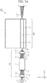
- FIG. 3A is a side view illustrating the main part of the laser amplifier according to the first embodiment.
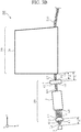
- FIG. 3B is a plan view illustrating the main part of the laser amplifier according to the first embodiment.
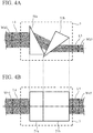
- FIG. 4A is a plan view illustrating an anamorphic prism of an input optical system of the laser amplifier according to the first embodiment.
- FIG. 4B is a side view illustrating the anamorphic prism of the input optical system of the laser amplifier according to the first embodiment.
- a laser amplifier 300 of the first embodiment will be described with reference to FIGS. 1 to 4 .
- L1 to L10 represent laser light to be amplified by the laser amplifier 300, that is, signal light.
- Symbols L1 to L8 denote signal light before amplification
- L9 denotes signal light during amplification
- L10 denotes signal light after amplification. Note that excitation light is not illustrated.
- symbol 1 denotes a core layer.
- the core layer 1 is made of a laser medium that is an isotropic medium.
- the core layer 1 is made of, for example, phosphate glass, silicate glass, fluoride glass, YAG, YGAG, ceramic YAG, or ceramic Lu2O3.
- the core layer 1 is quadrangular and has four side faces 11a, 11b, 11c, and 11d.
- the side faces 11a and 11b are arranged so as to face each other but are not parallel to each other.
- the side faces 11c and 11d are arranged so as to face each other and are parallel to each other. That is, the core layer 1 is trapezoidal.
- the side face 11a has a portion (hereinafter referred to as "light incident surface") 12 to which signal light L8 before amplification is input.
- An antireflection film is provided on the light incident surface 12, and a high reflection film is provided on the remaining portion of the side face 11a.
- the anti-reflection film is formed by anti reflection (AR) coating.
- the high reflection film is formed by high reflection (HR) coating.
- the incident angle ⁇ v (not illustrated) in the vertical direction is set to, for example, zero degrees.
- the incident angle ⁇ h in the horizontal direction is set to a value larger than zero degrees.
- the side face 11b has a portion (hereinafter referred to as "light emitting surface") 13 from which the signal light L10 after amplification is output.
- the light emitting surface 13 is disposed so as to face the light incident surface 12, for example.
- An antireflection film is provided on the light emitting surface 13, and a high reflection film is provided on the remaining portion of the side face 11b.
- the antireflection film is formed by AR coating.
- the high reflection film is formed by HR coating.
- the core layer 1 is disposed between two clad layers 2a and 2b.
- Each of the clad layers 2a and 2b is made of an isotropic medium and has a refractive index lower than that of the core layer 1.
- each of the clad layers 2a and 2b is made of, for example, phosphate glass, silicate glass, fluoride glass, YAG, YGAG, ceramic YAG, ceramic Lu2O3, a SiO2 film, a Ta2O5 film, an Al2O3 film, or a MgF2 film.
- the clad layer 2a that is one of the two clad layers 2a and 2b may be referred to as an "upper clad layer”.
- the other clad layer 2b may be referred to as a "lower clad layer”.
- the main part of a planar optical waveguide 100 includes the upper clad layer 2a, the core layer 1, and the lower clad layer 2b. That is, the planar optical waveguide 100 has a laminated structure including the upper clad layer 2a, the core layer 1, and the lower clad layer 2b.
- a signal light source 3 outputs signal light L1. That is, the signal light source 3 has a surface (hereinafter, referred to as "light emitting surface") from which the signal light L1 is output.
- the signal light source 3 includes a laser light source having a single wavelength ⁇ .
- the signal light source 3 includes a fiber laser, a semiconductor laser, or a solid-state laser.
- the wavelength ⁇ of the signal light L1 is set to a value that corresponds to the energy equivalent to the energy possessed by electrons in the laser medium of the core layer 1 when a population inversion state is formed.
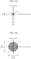
- FIG. 5A is a cross-sectional view of the output light L1 from the signal light source 3. More specifically, FIG. 5A is a cross-sectional view of the output light L1 on the light emitting surface of the signal light source 3.
- Wv1 denotes the vertical beam width of the output light L1 on the light emitting surface of the signal light source 3.
- Wh1 denotes the horizontal beam width of the output light L1 on the light emitting surface of the signal light source 3.
- the signal light source 3 includes a fiber laser. Therefore, the cross-sectional shape of the output light L1 by the signal light source 3 is circular.
- the output light L1 from the signal light source 3 is propagated in the air while gradually spreading and is input to a collimating lens 4. That is, the output light L1 from the signal light source 3 is input light L2 to the collimating lens 4.
- the collimating lens 4 converts the input light L2 into parallel light L3 and outputs the parallel light L3 that has been converted.
- a front surface 41 of the collimating lens 4 is substantially spherical, and a back surface 42 of the collimating lens 4 is substantially flat.
- the collimating lens 4 has a focal point on the back surface 42 side.
- the light emitting surface of the signal light source 3 is disposed at a position that corresponds to the focal point of the collimating lens 4.
- f1 denotes the focal length of the collimating lens 4.
- FIG. 5B is a cross-sectional view of the output light L3 from the collimating lens 4.
- Wv3 denotes the vertical beam width of the output light L3 by the collimating lens 4.
- Wh3 denotes the horizontal beam width of the output light L3 by the collimating lens 4.
- the cross-sectional shape of the output light L3 by the collimating lens 4 is circular. This is because the cross-sectional shape of the output light L1 by the signal light source 3 is circular, and thus the cross-sectional shape of the input light L2 to the collimating lens 4 is also circular.
- the output light L3 from the collimating lens 4 is propagated in the air and is input to an anamorphic prism 5. That is, the output light L3 from the collimating lens 4 is input light L4 for the anamorphic prism 5.
- the anamorphic prism 5 outputs parallel light L5 having a reduced horizontal beam width as compared to that of the input light L4.
- the anamorphic prism 5 includes a pair of prisms 51a and 51b.
- FIG. 5C is a cross-sectional view of the output light L5 by the anamorphic prism 5.
- Wv4 denotes the vertical beam width of the input light L4 to the anamorphic prism 5.
- the vertical beam width Wv4 of the input light L4 is equivalent to the vertical beam width Wv3 of the output light L3 by the collimating lens 4.
- Wh4 denotes the horizontal beam width of the input light L4 to the anamorphic prism 5.
- the horizontal beam width Wh4 of the input light L4 is equivalent to the horizontal beam width Wh3 of the output light L3 by the collimating lens 4.
- Wv5 denotes the vertical beam width of the output light L5 by the anamorphic prism 5.
- the vertical beam width Wv5 of the output light L5 is equivalent to the vertical beam width Wv4 of the input light L4.
- Wh5 denotes the horizontal beam width of the output light L5 by the anamorphic prism 5.
- the horizontal beam width Wh5 of the output light L5 is smaller than the horizontal beam width Wh4 of the input light L4. This is due to the beam width reducing function of the anamorphic prism 5.
- the output light L5 from the anamorphic prism 5 is propagated in the air and is input to the cylindrical lens 6. That is, the output light L5 from the anamorphic prism 5 is input light L6 to the cylindrical lens 6.
- the cylindrical lens 6 condenses the input light L6 in the vertical direction.
- Output light L7 from the cylindrical lens 6 is propagated in the air and is input to the core layer 1. That is, the output light L7 from the cylindrical lens 6 is input light L8 to the core layer 1.
- a front surface 61 of the cylindrical lens 6 has a substantially cylindrical curved surface shape, and a back surface 62 of the cylindrical lens 6 has a substantially flat surface shape.
- the cylindrical lens 6 has a focal point on the front surface 61 side.
- the light incident surface 12 of the core layer 1 is disposed at a position that corresponds to the focal point of the cylindrical lens 6.
- f2 denotes the focal length of the cylindrical lens 6.
- FIG. 5D is a cross-sectional view of the input light L8 to the core layer 1. More specifically, it is a cross-sectional view of the input light L8 on the light incident surface 12 of the core layer 1.
- Wv8 denotes the vertical beam width of the input light L8 on the light incident surface 12 of the core layer 1.
- Wh8 denotes the horizontal beam width of the input light L8 on the light incident surface 12 of the core layer 1.
- the horizontal beam width Wh8 of the input light L8 on the light incident surface 12 of the core layer 1 is equivalent to the horizontal beam width Wh6 of the input light L6 to the cylindrical lens 6, that is, equivalent to the horizontal beam width Wh5 of the output light L5 by the anamorphic prism 5.
- the vertical beam width Wv8 of the input light L8 on the light incident surface 12 of the core layer 1 is smaller than the vertical beam width Wv6 of the input light L6 to the cylindrical lens 6, that is, smaller than the vertical beam width Wv5 of the output light L5 from the anamorphic prism 5. This is due to the light condensing function of the cylindrical lens 6.
- the vertical beam width Wv8 of the input light L8 on the light incident surface 12 of the core layer 1 is set to a value smaller than the horizontal beam width Wh8 of the input light L8 on the light incident surface 12 of the core layer 1. More specifically, the vertical beam width Wv8 of the input light L8 on the light incident surface 12 of the core layer 1 is set to a value less than or equal to the thickness t of the core layer 1. Therefore, it is possible to prevent the output light L7 from the cylindrical lens 6 from being emitted to the outside of the core layer 1. As a result, the coupling efficiency between the input optical system 200 and the planar optical waveguide 100 can be improved.
- the main part of the input optical system 200 includes the collimating lens 4, the anamorphic prism 5, and the cylindrical lens 6.
- the main part of the laser amplifier 300 includes the planar optical waveguide 100 and the input optical system 200.
- d indicates the installation interval between the cylindrical lens 6 and the planar optical waveguide 100, that is, the installation interval between the input optical system 200 and the planar optical waveguide 100.
- an excitation light source (not illustrated) outputs excitation light.
- the excitation light that has been output is input to the core layer 1 from the side face 11c or the side face 11d.
- the excitation light that has been input is absorbed by the laser medium of the core layer 1, thereby forming a population inversion state.
- the signal light source 3 outputs the signal light L1.
- the signal light L8 is input from the light incident surface 12 to the core layer 1.
- the signal light L9 that has been input is propagated inside the core layer 1, thereby amplifying the signal light L9 that has been input.
- each of the clad layers 2a and 2b has a refractive index lower than that of the core layer 1. Therefore, when the signal light L9 is propagated inside the core layer 1, the signal light L9 is totally reflected at the boundary surface between the core layer 1 and the upper clad layer 2a and at the boundary surface between the core layer 1 and the lower clad layer 2b. As a result, it is possible to suppress the signal light L9 from leaking from the core layer 1 to the clad layers 2a and 2b.
- a high reflection film is provided for a portion of the side face 11a excluding the light incident surface 12, and a high reflection film is provided for a portion of the side face 11b excluding the light emitting surface 13.
- the side faces 11a and 11b are arranged nonparallel to each other.
- the incident angle ⁇ h of the signal light L8 with respect to the core layer 1 is set to a value larger than zero degrees.
- the signal light L9 is reflected by the side faces 11a and 11b a plurality of times when the signal light L9 is propagated inside the core layer 1. More specifically, the signal light L9 is alternately reflected by the side faces 11a and 11b. As a result, as illustrated in FIG. 1 or 2 , the signal light L9 is propagated in a zigzag manner. As a result, the propagation path length of the signal light L9 in the laser medium can be increased with respect to the dimension of the core layer 1. Therefore, the gain of the laser amplifier 300 can be improved.
- the incident angle ⁇ h it is preferable to set the incident angle ⁇ h to an appropriate value depending on the dimensions of the core layer 1 and a required propagation path length of the signal light L9 (that is, a required number of times of reflection of the signal light L9).
- the conventional laser amplifier 300' has a planar optical waveguide 100'.
- the planar optical waveguide 100' has a laminated structure including an upper clad layer 2a', a core layer 1', and a lower clad layer 2b'.
- L1' to L3' and L6' to L8' denote signal light before amplification
- L10' denotes signal light after amplification.
- a signal light source 3' outputs signal light L1'.
- the output light L1' from the signal light source 3' is input light L2' to a collimating lens 4'.
- the collimating lens 4' converts the input light L2' to parallel light L3' and outputs the parallel light L3' that has been converted.
- a light emitting surface (not illustrated) of the signal light source 3' is disposed at a position that corresponds to the focal point of the collimating lens 4'.
- f1' denotes the focal length of the collimating lens 4'.
- the output light L3' from the collimating lens 4' is input light L6' to a cylindrical lens 6'.
- the cylindrical lens 6' condenses the input light L6' in the vertical direction.
- Output light L7' from the cylindrical lens 6' is input light L8' to the core layer 1'.
- Alight incident surface (not illustrated) of the core layer 1' is disposed at a position that corresponds to the focal point of the cylindrical lens 6'.
- f2' denotes the focal length of the cylindrical lens 6'.
- the main part of the input optical system 200' includes the collimating lens 4' and the cylindrical lens 6'.
- the main part of the laser amplifier 300' includes the planar optical waveguide 100' and the input optical system 200'.
- d' denotes the installation interval between the cylindrical lens 6' and the planar optical waveguide 100', that is, the installation interval between the input optical system 200' and the planar optical waveguide 100'.
- the vertical beam width Wv8' of the input light L8' on the light incident surface of the core layer 1' can be reduced by setting the vertical beam width Wv3' of the output light L3' from the collimating lens 4' to a large value or by setting the focal length f2' of the cylindrical lens 6' to a small value.
- the horizontal beam width Wh8' of the input light L8' on the light incident surface of the core layer 1' can be reduced by setting the horizontal beam width Wh3' of the output light L3' from the collimating lens 4' to a small value.
- the beam widths Wv3' and Wh3' of the output light L3' from the collimating lens 4' have values corresponding to the focal length f1' of the collimating lens 4'. That is, by increasing the focal length f1', both the beam widths Wv3' and Wh3' increase. On the other hand, by reducing the focal length f1', both the beam widths Wv3' and Wh3' decrease.
- the beam widths Wv3' and Wh3' are set by using the focal length f1' of the collimating lens 4'. Therefore, it is difficult to set one of the beam widths Wv3' and Wh3' to a large value while setting the other one of the beam widths Wv3' and Wh3' to a small value.
- the anamorphic prism 5 is arranged between the collimating lens 4 and the cylindrical lens 6.
- the focal length f2 of the cylindrical lens 6 can be set to a large value.
- the laser amplifier 300 of the first embodiment uses the cylindrical lens 6 having the focal length f2 that is larger than that of the conventional laser amplifier 300', and thus it is possible to reduce the beam widths Wv8 and Wh8 of the input light L8 on the light incident surface 12 of the core layer 1.
- the installation interval d between the input optical system 200 and the planar optical waveguide 100 is larger than that of the conventional laser amplifier 300'.
- the focal length f2' is required to be set to a value corresponding to the required beam widths Wv8' and Wh8' on the basis of the above equation (3). For example, let us assume that the values of required beam widths Wv8' and Wh8' satisfy the conditions expressed by the following inequation (4). In this case, the focal length f2' is required to be set to a value larger than 1 millimeter and smaller than 6 millimeters. 1.0 ⁇ ⁇ ⁇ Wv8' ⁇ Wh8' / 4 ⁇ ⁇ ⁇ 6.0
- the focal length of an off-the-shelf cylindrical lens is set to a value less than or equal to 1 millimeter or a value greater than or equal to of 6 millimeters. Therefore, in a case where the values of required beam widths Wv8' and Wh8' satisfy the conditions expressed in the above inequation (4), off-the-shelf products cannot be used for the cylindrical lens 6'. Using a custom-made product for the cylindrical lens 6' causes a problem of increased development cost and manufacturing cost of the input optical system 200'.
- the cylindrical lens 6 having a desired focal length f2 that includes a value within the focal length range of off-the-shelf products (that is, a range of less than or equal to 1 millimeter or a range of greater than or equal to 6 millimeters).
- a focal length f2 that includes a value within the focal length range of off-the-shelf products (that is, a range of less than or equal to 1 millimeter or a range of greater than or equal to 6 millimeters).
- the comparative laser amplifier 300" has a planar optical waveguide 100".
- the planar optical waveguide 100" has a laminated structure including an upper clad layer 2a", a core layer 1" and a lower clad layer 2b".
- L1" to L3", L6" to L8", L11", and L12" denote signal light before amplification
- L10" denotes signal light after amplification.
- a signal light source 3" outputs signal light L1".
- the output light L1" from the signal light source 3" is input light L2" to a collimating lens 4".
- the collimating lens 4" converts the input light L2" to parallel light L3” and outputs the parallel light L3" that has been converted.
- a light emitting surface (not illustrated) of the signal light source 3" is disposed at a position that corresponds to the focal point of the collimating lens 4".
- f1" denotes the focal length of the collimating lens 4".
- the output light L3" from the collimating lens 4" is input light L11" to a cylindrical lens 7".
- the cylindrical lens 7" condenses the input light L11" in the horizontal direction.
- Output light L12" from the cylindrical lens 7" is input light L6" to a cylindrical lens 6".
- the cylindrical lens 6" condenses the input light L6" in the vertical direction.
- Output light L7" from the cylindrical lens 6" is input light L8" to the core layer 1".
- the light incident surface (not illustrated) of the core layer 1" is disposed at a position corresponding to the focal point of the cylindrical lens 7" and is disposed at a position corresponding to the focal point of the cylindrical lens 6".
- f3" denotes the focal length of the cylindrical lens 7
- f2" denotes the focal length of the cylindrical lens 6".
- the main part of the input optical system 200" includes the collimating lens 4", the cylindrical lens 7", and the cylindrical lens 6".
- the main part of the laser amplifier 300" includes the planar optical waveguide 100" and the input optical system 200".
- d denotes the installation interval between the cylindrical lens 6" and the planar optical waveguide 100", that is, the installation interval between the input optical system 200" and the planar optical waveguide 100".
- the laser amplifier 300 of the first embodiment implements a required vertical beam width Wv8, using the light condensing function of the cylindrical lens 6.
- the comparative laser amplifier 300" implements a required vertical beam width Wv8", using the light condensing function of the cylindrical lens 6".
- the comparative laser amplifier 300" implements a required horizontal beam width Wh8", using the light condensing function of the cylindrical lens 7". Therefore, the horizontal beam width Wh9" (not illustrated) of signal light L9” gradually increases when the signal light L9" input to the core layer 1" is propagated inside the core layer 1". As a result, the horizontal beam width Wh10" of output light L10" on the light emitting surface (not illustrated) of the core layer 1" is greater than the horizontal beam width Wh8" of the input light L8"on the light incident surface of the core layer 1. Moreover, the horizontal beam width Wh10" of the output light L10” gradually increases when the output light L10" from the core layer 1" is propagated in the air.
- output optical system another optical system
- the coupling efficiency between the planar optical waveguide 100" and the output optical system decreases.
- the laser amplifier 300 of the first embodiment implements a required horizontal beam width Wh8, using the beam width reduction function of the anamorphic prism 5. Therefore, it is possible to suppress the horizontal beam width Wh9 of the signal light L9 from gradually increasing when the signal light L9 is propagated inside the core layer 1. As a result, it is possible to make the horizontal beam width Wh10 of the output light L10 on the light emitting surface 13 of the core layer 1 substantially equivalent to the horizontal beam width Wh8 of the input light L8 on the light incident surface 12 of the core layer 1. It is also possible to suppress the horizontal beam width Wh10 of the output light L10 from gradually increasing when the output light L10 from the core layer 1 is propagated in the air. As a result, the coupling efficiency between the planar optical waveguide 100 and the output optical system can be improved.
- the side face 11a of the core layer 1 may include a portion (hereinafter referred to as "light incident and emitting surface") 14 where the signal light L8 before amplification is input and the signal light L10 after amplification is output.
- the outward path of the signal light L9 inside the core layer 1 may be a similar path to the return path of the signal light L9 inside the core layer 1.
- a light incident and emitting surface 14 may be included on the side face 11a of the core layer 1 as illustrated in FIG. 8B .
- the outward path of the signal light L9 inside the core layer 1 may be a different path from the return path of the signal light L9 inside the core layer 1.
- a high reflection film may be provided on the side face 11d.
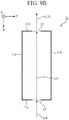
- the core layer 1 may have a rectangular shape, the side faces 11a and 11b may correspond to the long sides of the rectangle, and the side faces 11c and 11d may correspond to the short sides of the rectangle.
- the light incident and emitting surface 14 may be included on the side face 11c.
- the propagation path of the signal light L9 extends along the longitudinal direction of the core layer 1.
- a high reflection film may be provided on the side face 11d.
- the core layer 1 may have a rectangular shape, the side faces 11a and 11b may correspond to the long sides of the rectangle, and the side faces 11c and 11d may correspond to the short sides of the rectangle.
- the light incident surface 12 may be included on the side face 11c, and the light emitting surface 13 may be included on the side face 11d.
- the propagation path of the signal light L9 extends along the longitudinal direction of the core layer 1. As a result, it is possible to ensure the propagation path length of the signal light L9 while eliminating the need for reflection of the signal light L9 by the side faces 11a and 11b.
- the direction in which the beam width is reduced by the anamorphic prism 5 (hereinafter referred to as the "first direction") is not limited to the horizontal direction.
- the light condensing direction by the cylindrical lens 6 (hereinafter referred to as the "second direction”) is not limited to the vertical direction.
- the anamorphic prism 5 may reduce the beam width in the vertical direction, and the cylindrical lens 6 may condense light in the horizontal direction.
- the first direction to the horizontal direction and the second direction to the vertical direction, from the viewpoint of making the vertical beam width Wv8 further smaller than the horizontal beam width Wh8.
- the first direction to the horizontal direction and the second direction to the vertical direction.
- the laser amplifier 300 of the first embodiment includes the planar optical waveguide 100 for laser amplification and the input optical system 200 for inputting signal light to the core layer 1 of the planar optical waveguide 100.
- the input optical system 200 includes: the collimating lens 4 for converting output light from the signal light source 3 into parallel light; the anamorphic prism 5 for reducing the beam width in the first direction of output light from the collimating lens 4; and the cylindrical lens 6 for collecting output light from the anamorphic prism 5 in the second direction, and output light from the cylindrical lens 6 is input to the core layer 1.
- the anamorphic prism 5 Since the anamorphic prism 5 is included, it is not necessary to set the beam widths Wv3 and Wh3 of the output light L3 from the collimating lens 4 to small values in order to reduce the beam widths Wv8 and Wh8 of the input light L8 on the light incident surface 12 of the core layer 1. Therefore, it is not necessary to set the focal length f2 of the cylindrical lens 6 to a small value. Since the installation interval d between the input optical system 200 and the planar optical waveguide 100 is large, it is possible to facilitate adjustment of the installation position of the input optical system 200 with respect to the planar optical waveguide 100.
- the planar optical waveguide 100 has the laminated structure including the upper clad layer 2a, the core layer 1, and the lower clad layer 2b, and the first direction is set to be orthogonal to the lamination direction in the laminated structure.
- a required horizontal beam width Wh8 using the beam width reduction function of the anamorphic prism 5.
- the coupling efficiency between the planar optical waveguide 100 and the output optical system can be improved.
- the planar optical waveguide 100 has the laminated structure including the upper clad layer 2a, the core layer 1, and the lower clad layer 2b, and the second direction is set to be parallel with the lamination direction in the laminated structure.
- a required vertical beam width Wv8 can be implemented, using the light condensing function of the cylindrical lens 6. Specifically, for example, it is possible to implement a vertical beam width Wv8 that is further smaller than the horizontal beam width Wh8. It is further possible to implement a vertical beam width Wv8 that is less than or equal to the wall thickness t of the core layer 1.
- the focal length f2 of the cylindrical lens 6 is set to a value greater than or equal to 6 millimeters.
- an off-the-shelf product can be used as the cylindrical lens 6.
- the development cost and the manufacturing cost of the input optical system 200 can be reduced.
- antireflection films are provided for a portion to which the signal light is input (light incident surface 12) and for a portion from which the signal light is output (light emitting surface 13), and high reflection films are provided for the other portions of the side faces 11a and 11b.
- the planar optical waveguide 100 has a structure in which the signal light input to the core layer 1 is reflected by the side faces 11a and 11b of the core layer 1 a plurality of times when the signal light is propagated inside the core layer 1.
- the propagation path length of the signal light L9 in the laser medium can be made longer than the dimension of the core layer 1.
- the gain of the laser amplifier 300 can be improved.
- the planar optical waveguide 100 has a laminated structure including the upper clad layer 2a, the core layer 1, and the lower clad layer 2b, and, of beam widths of the signal light input to the core layer 1, a beam width in a direction orthogonal to the lamination direction in the laminated structure is set to a value less than or equal to the thickness t of the core layer 1. As a result, the coupling efficiency between the input optical system 200 and the planar optical waveguide 100 can be improved.
- a laser amplifier of the present invention can be used, for example, for amplifying laser light for measurement or communication.
- 1 core layer
- 2a clad layer (upper clad layer)
- 2b clad layer (lower clad layer)
- 3 signal light source
- 4 collimating lens
- 5 anamorphic prism
- 6 cylindrical lens
- 11a side face
- 11b side face
- 11c side face
- 11d side face
- 12 light incident surface
- 13 light emitting surface
- 14 light incident and emitting surface
- 51a prism
- 51b prism
- 61 front surface
- 62 back surface
- 100 planar optical waveguide
- 200 input optical system
- 300 laser amplifier
Landscapes
- Physics & Mathematics (AREA)
- Electromagnetism (AREA)
- Optics & Photonics (AREA)
- Engineering & Computer Science (AREA)
- Plasma & Fusion (AREA)
- General Physics & Mathematics (AREA)
- Lasers (AREA)
- Optical Couplings Of Light Guides (AREA)
- Optical Integrated Circuits (AREA)
Abstract
Description
- The present invention relates to a laser amplifier.
- In the related art, laser amplifiers of a planar waveguide type have been developed (see, for example, Patent Literature 1). A laser amplifier of the planar waveguide type includes a planar optical waveguide for laser amplification. The planar optical waveguide has a laminated structure in which one core layer is disposed between two clad layers. The core layer is made of a laser medium, and each clad layer has a refractive index lower than that of the core layer. Excitation light as well as laser light to be amplified, that is, so-called "signal light" is input to the core layer. With the input excitation light absorbed by the laser medium, a so-called "population inversion state" is formed. When the input signal light is propagated inside the core layer in this state, the input signal light is amplified.
- Patent Literature 1:
JP 2013-89790 A - Hereinafter, the direction along the lamination direction in a laminated structure of a planar optical waveguide is referred to as the "vertical direction". Meanwhile, the direction along individual layers in the laminated structure, that is, the direction orthogonal to the lamination direction in the laminated structure is referred to as the "horizontal direction". Moreover, the beam width of signal light in the vertical direction may be referred to as "vertical beam width". The beam width of signal light in the horizontal direction may be referred to as "horizontal beam width". Furthermore, signal light input to each optical member and the signal light that has been input may be collectively referred to as "input light". Signal light output by each optical member and the signal light that has been output may be collectively referred to as "output light".
- A laser amplifier of a planar waveguide type has an optical system (hereinafter referred to as "input optical system") for inputting signal light to the core layer of a planar optical waveguide. In recent years, from the viewpoint of meeting the demand for miniaturization of planar optical waveguides, it has been desired to reduce the beam width of input light to the core layer. In particular, from the viewpoint of meeting the demand for the thinning of the core layer, it has been desired to make the vertical beam width of the input light to be even smaller than the horizontal beam width of the input light.
- As will be described later with reference to
FIG. 6 , an input optical system in a conventional laser amplifier of the planar waveguide type includes a collimating lens and a cylindrical lens. In a conventional laser amplifier of the planar waveguide type, in order to reduce the beam width of input light to the core layer, it is required to set the focal length of the cylindrical lens to a small value. Due to the small focal length of the cylindrical lens, the installation interval between the input optical system and the planar optical waveguide is small. Therefore, there is a problem that it is difficult to adjust the installation position of the input optical system with respect to the planar optical waveguide when the laser amplifier is assembled. - The present invention has been made to solve the disadvantage as described above, and an object of the present invention is to provide a laser amplifier in which it is easy to adjust the installation position of an input optical system with respect to a planar optical waveguide.
- A laser amplifier of the present invention includes a planar optical waveguide for laser amplification, and an input optical system for inputting signal light to a core layer of the planar optical waveguide, in which the input optical system includes: a collimating lens for converting output light from a signal light source into parallel light; an anamorphic prism for reducing a beam width in a first direction of output light from the collimating lens; and a cylindrical lens for collecting output light from the anamorphic prism in a second direction, and output light from the cylindrical lens is input to the core layer.
- According to the present invention configured as described above, it is possible to obtain a laser amplifier in which it is easy to adjust the installation position of an input optical system with respect to a planar optical waveguide.
-
-
FIG. 1 is a perspective view illustrating the main part of a laser amplifier according to a first embodiment. -
FIG. 2 is a plan view illustrating a core layer of a planar optical waveguide of the laser amplifier according to the first embodiment. -
FIG. 3A is a side view illustrating the main part of the laser amplifier according to the first embodiment. -
FIG. 3B is a plan view illustrating the main part of the laser amplifier according to the first embodiment. -
FIG. 4A is a plan view illustrating an anamorphic prism of an input optical system of the laser amplifier according to the first embodiment.FIG. 4B is a side view illustrating the anamorphic prism of the input optical system of the laser amplifier according to the first embodiment. -
FIG. 5A is a cross-sectional view of output light from a signal light source. -
FIG. 5B is a cross-sectional view of output light from a collimating lens. -
FIG. 5C is a cross-sectional view of output light from an anamorphic prism. -
FIG. 5D is a cross-sectional view of input light to a core layer. -
FIG. 6A is a side view illustrating the main part of a laser amplifier of the related art. -
FIG. 6B is a plan view illustrating the main part of the laser amplifier of the related art. -
FIG. 7A is a side view illustrating the main part of a laser amplifier for comparison with the laser amplifier according to the first embodiment. -
FIG. 7B is a plan view illustrating the main part of the laser amplifier for comparison with the laser amplifier according to the first embodiment. -
FIG. 8A is a plan view illustrating another core layer of the planar optical waveguide of the laser amplifier according to the first embodiment. -
FIG. 8B is a plan view illustrating another core layer of the planar optical waveguide of the laser amplifier according to the first embodiment. -
FIG. 9A is a plan view illustrating another core layer of the planar optical waveguide of the laser amplifier according to the first embodiment. -
FIG. 9B is a plan view illustrating another core layer of the planar optical waveguide of the laser amplifier according to the first embodiment. - To describe the present invention further in detail, an embodiment for carrying out the present invention will be described below with reference to the accompanying drawings.
-
FIG. 1 is a perspective view illustrating the main part of a laser amplifier according to a first embodiment.FIG. 2 is a plan view illustrating a core layer of a planar optical waveguide of the laser amplifier according to the first embodiment.FIG. 3A is a side view illustrating the main part of the laser amplifier according to the first embodiment.FIG. 3B is a plan view illustrating the main part of the laser amplifier according to the first embodiment.FIG. 4A is a plan view illustrating an anamorphic prism of an input optical system of the laser amplifier according to the first embodiment.FIG. 4B is a side view illustrating the anamorphic prism of the input optical system of the laser amplifier according to the first embodiment. Alaser amplifier 300 of the first embodiment will be described with reference toFIGS. 1 to 4 . - In the figures, L1 to L10 represent laser light to be amplified by the
laser amplifier 300, that is, signal light. Symbols L1 to L8 denote signal light before amplification, L9 denotes signal light during amplification, and L10 denotes signal light after amplification. Note that excitation light is not illustrated. - In the figures,
symbol 1 denotes a core layer. Thecore layer 1 is made of a laser medium that is an isotropic medium. Specifically, thecore layer 1 is made of, for example, phosphate glass, silicate glass, fluoride glass, YAG, YGAG, ceramic YAG, or ceramic Lu2O3. - As illustrated in
FIG. 2 , thecore layer 1 is quadrangular and has four side faces 11a, 11b, 11c, and 11d. The side faces 11a and 11b are arranged so as to face each other but are not parallel to each other. The side faces 11c and 11d are arranged so as to face each other and are parallel to each other. That is, thecore layer 1 is trapezoidal. - The
side face 11a has a portion (hereinafter referred to as "light incident surface") 12 to which signal light L8 before amplification is input. An antireflection film is provided on thelight incident surface 12, and a high reflection film is provided on the remaining portion of theside face 11a. The anti-reflection film is formed by anti reflection (AR) coating. The high reflection film is formed by high reflection (HR) coating. - Of the incident angles θv and θh of the signal light L8 with respect to the
core layer 1, the incident angle θv (not illustrated) in the vertical direction is set to, for example, zero degrees. Meanwhile, the incident angle θh in the horizontal direction is set to a value larger than zero degrees. - The
side face 11b has a portion (hereinafter referred to as "light emitting surface") 13 from which the signal light L10 after amplification is output. Thelight emitting surface 13 is disposed so as to face thelight incident surface 12, for example. An antireflection film is provided on thelight emitting surface 13, and a high reflection film is provided on the remaining portion of theside face 11b. The antireflection film is formed by AR coating. The high reflection film is formed by HR coating. - The
core layer 1 is disposed between twoclad layers clad layers core layer 1. Specifically, for example, each of theclad layers - Hereinafter, the
clad layer 2a that is one of the twoclad layers clad layer 2b may be referred to as a "lower clad layer". The main part of a planaroptical waveguide 100 includes the upper cladlayer 2a, thecore layer 1, and the lowerclad layer 2b. That is, the planaroptical waveguide 100 has a laminated structure including the upper cladlayer 2a, thecore layer 1, and the lowerclad layer 2b. - A
signal light source 3 outputs signal light L1. That is, thesignal light source 3 has a surface (hereinafter, referred to as "light emitting surface") from which the signal light L1 is output. Thesignal light source 3 includes a laser light source having a single wavelength λ. Specifically, for example, thesignal light source 3 includes a fiber laser, a semiconductor laser, or a solid-state laser. The wavelength λ of the signal light L1 is set to a value that corresponds to the energy equivalent to the energy possessed by electrons in the laser medium of thecore layer 1 when a population inversion state is formed. -
FIG. 5A is a cross-sectional view of the output light L1 from thesignal light source 3. More specifically,FIG. 5A is a cross-sectional view of the output light L1 on the light emitting surface of thesignal light source 3. In the figure, Wv1 denotes the vertical beam width of the output light L1 on the light emitting surface of thesignal light source 3. Furthermore, Wh1 denotes the horizontal beam width of the output light L1 on the light emitting surface of thesignal light source 3. In the example illustrated inFIG. 5A , thesignal light source 3 includes a fiber laser. Therefore, the cross-sectional shape of the output light L1 by thesignal light source 3 is circular. - The output light L1 from the
signal light source 3 is propagated in the air while gradually spreading and is input to acollimating lens 4. That is, the output light L1 from thesignal light source 3 is input light L2 to thecollimating lens 4. Thecollimating lens 4 converts the input light L2 into parallel light L3 and outputs the parallel light L3 that has been converted. - A
front surface 41 of thecollimating lens 4 is substantially spherical, and aback surface 42 of thecollimating lens 4 is substantially flat. Thecollimating lens 4 has a focal point on theback surface 42 side. The light emitting surface of thesignal light source 3 is disposed at a position that corresponds to the focal point of thecollimating lens 4. In the figure, f1 denotes the focal length of thecollimating lens 4. -
FIG. 5B is a cross-sectional view of the output light L3 from thecollimating lens 4. In the figure, Wv3 denotes the vertical beam width of the output light L3 by thecollimating lens 4. Meanwhile, Wh3 denotes the horizontal beam width of the output light L3 by thecollimating lens 4. In the example illustrated inFIG. 5B , the cross-sectional shape of the output light L3 by thecollimating lens 4 is circular. This is because the cross-sectional shape of the output light L1 by thesignal light source 3 is circular, and thus the cross-sectional shape of the input light L2 to thecollimating lens 4 is also circular. - The output light L3 from the
collimating lens 4 is propagated in the air and is input to ananamorphic prism 5. That is, the output light L3 from thecollimating lens 4 is input light L4 for theanamorphic prism 5. Theanamorphic prism 5 outputs parallel light L5 having a reduced horizontal beam width as compared to that of the input light L4. As illustrated inFIG. 4 , theanamorphic prism 5 includes a pair ofprisms FIG. 5C is a cross-sectional view of the output light L5 by theanamorphic prism 5. - In the figure, Wv4 denotes the vertical beam width of the input light L4 to the
anamorphic prism 5. The vertical beam width Wv4 of the input light L4 is equivalent to the vertical beam width Wv3 of the output light L3 by thecollimating lens 4. Meanwhile, Wh4 denotes the horizontal beam width of the input light L4 to theanamorphic prism 5. The horizontal beam width Wh4 of the input light L4 is equivalent to the horizontal beam width Wh3 of the output light L3 by thecollimating lens 4. - In addition, Wv5 denotes the vertical beam width of the output light L5 by the
anamorphic prism 5. The vertical beam width Wv5 of the output light L5 is equivalent to the vertical beam width Wv4 of the input light L4. Meanwhile, Wh5 denotes the horizontal beam width of the output light L5 by theanamorphic prism 5. The horizontal beam width Wh5 of the output light L5 is smaller than the horizontal beam width Wh4 of the input light L4. This is due to the beam width reducing function of theanamorphic prism 5. - The output light L5 from the
anamorphic prism 5 is propagated in the air and is input to thecylindrical lens 6. That is, the output light L5 from theanamorphic prism 5 is input light L6 to thecylindrical lens 6. Thecylindrical lens 6 condenses the input light L6 in the vertical direction. Output light L7 from thecylindrical lens 6 is propagated in the air and is input to thecore layer 1. That is, the output light L7 from thecylindrical lens 6 is input light L8 to thecore layer 1. - A
front surface 61 of thecylindrical lens 6 has a substantially cylindrical curved surface shape, and aback surface 62 of thecylindrical lens 6 has a substantially flat surface shape. Thecylindrical lens 6 has a focal point on thefront surface 61 side. Thelight incident surface 12 of thecore layer 1 is disposed at a position that corresponds to the focal point of thecylindrical lens 6. In the figure, f2 denotes the focal length of thecylindrical lens 6. -
FIG. 5D is a cross-sectional view of the input light L8 to thecore layer 1. More specifically, it is a cross-sectional view of the input light L8 on thelight incident surface 12 of thecore layer 1. In the figure, Wv8 denotes the vertical beam width of the input light L8 on thelight incident surface 12 of thecore layer 1. Meanwhile, Wh8 denotes the horizontal beam width of the input light L8 on thelight incident surface 12 of thecore layer 1. - The horizontal beam width Wh8 of the input light L8 on the
light incident surface 12 of thecore layer 1 is equivalent to the horizontal beam width Wh6 of the input light L6 to thecylindrical lens 6, that is, equivalent to the horizontal beam width Wh5 of the output light L5 by theanamorphic prism 5. Meanwhile, the vertical beam width Wv8 of the input light L8 on thelight incident surface 12 of thecore layer 1 is smaller than the vertical beam width Wv6 of the input light L6 to thecylindrical lens 6, that is, smaller than the vertical beam width Wv5 of the output light L5 from theanamorphic prism 5. This is due to the light condensing function of thecylindrical lens 6. - The vertical beam width Wv8 of the input light L8 on the
light incident surface 12 of thecore layer 1 is set to a value smaller than the horizontal beam width Wh8 of the input light L8 on thelight incident surface 12 of thecore layer 1. More specifically, the vertical beam width Wv8 of the input light L8 on thelight incident surface 12 of thecore layer 1 is set to a value less than or equal to the thickness t of thecore layer 1. Therefore, it is possible to prevent the output light L7 from thecylindrical lens 6 from being emitted to the outside of thecore layer 1. As a result, the coupling efficiency between the inputoptical system 200 and the planaroptical waveguide 100 can be improved. - The main part of the input
optical system 200 includes thecollimating lens 4, theanamorphic prism 5, and thecylindrical lens 6. The main part of thelaser amplifier 300 includes the planaroptical waveguide 100 and the inputoptical system 200. In the figure, d indicates the installation interval between thecylindrical lens 6 and the planaroptical waveguide 100, that is, the installation interval between the inputoptical system 200 and the planaroptical waveguide 100. - Next, the operation by the
laser amplifier 300 for amplifying signal light will be described. - First, an excitation light source (not illustrated) outputs excitation light. The excitation light that has been output is input to the
core layer 1 from theside face 11c or theside face 11d. The excitation light that has been input is absorbed by the laser medium of thecore layer 1, thereby forming a population inversion state. - In this state, the
signal light source 3 outputs the signal light L1. As a result, the signal light L8 is input from thelight incident surface 12 to thecore layer 1. The signal light L9 that has been input is propagated inside thecore layer 1, thereby amplifying the signal light L9 that has been input. - Here, each of the
clad layers core layer 1. Therefore, when the signal light L9 is propagated inside thecore layer 1, the signal light L9 is totally reflected at the boundary surface between thecore layer 1 and the upper cladlayer 2a and at the boundary surface between thecore layer 1 and the lowerclad layer 2b. As a result, it is possible to suppress the signal light L9 from leaking from thecore layer 1 to theclad layers - Furthermore, a high reflection film is provided for a portion of the
side face 11a excluding thelight incident surface 12, and a high reflection film is provided for a portion of theside face 11b excluding thelight emitting surface 13. The side faces 11a and 11b are arranged nonparallel to each other. And, the incident angle θh of the signal light L8 with respect to thecore layer 1 is set to a value larger than zero degrees. - Therefore, the signal light L9 is reflected by the side faces 11a and 11b a plurality of times when the signal light L9 is propagated inside the
core layer 1. More specifically, the signal light L9 is alternately reflected by the side faces 11a and 11b. As a result, as illustrated inFIG. 1 or2 , the signal light L9 is propagated in a zigzag manner. As a result, the propagation path length of the signal light L9 in the laser medium can be increased with respect to the dimension of thecore layer 1. Therefore, the gain of thelaser amplifier 300 can be improved. - Note that the number of times the signal light L9 is reflected by the side faces 11a and 11b changes as the incident angle θh changes. As a result, the propagation path length of the signal light L9 changes. Therefore, it is preferable to set the incident angle θh to an appropriate value depending on the dimensions of the
core layer 1 and a required propagation path length of the signal light L9 (that is, a required number of times of reflection of the signal light L9). - Next, a conventional laser amplifier 300' will be described with reference to
FIG. 6 . Furthermore, advantageous effects of thelaser amplifier 300 of the first embodiment over the conventional laser amplifier 300' will be described. - As illustrated in
FIG. 6 , the conventional laser amplifier 300' has a planar optical waveguide 100'. The planar optical waveguide 100' has a laminated structure including an upperclad layer 2a', a core layer 1', and a lowerclad layer 2b'. In the figure, L1' to L3' and L6' to L8' denote signal light before amplification, and L10' denotes signal light after amplification. - A signal light source 3' outputs signal light L1'. The output light L1' from the signal light source 3' is input light L2' to a collimating lens 4'. The collimating lens 4' converts the input light L2' to parallel light L3' and outputs the parallel light L3' that has been converted. A light emitting surface (not illustrated) of the signal light source 3' is disposed at a position that corresponds to the focal point of the collimating lens 4'. In the figure, f1' denotes the focal length of the collimating lens 4'.
- The output light L3' from the collimating lens 4' is input light L6' to a cylindrical lens 6'. The cylindrical lens 6' condenses the input light L6' in the vertical direction. Output light L7' from the cylindrical lens 6' is input light L8' to the core layer 1'. Alight incident surface (not illustrated) of the core layer 1' is disposed at a position that corresponds to the focal point of the cylindrical lens 6'. In the figure, f2' denotes the focal length of the cylindrical lens 6'.
- The main part of the input optical system 200' includes the collimating lens 4' and the cylindrical lens 6'. The main part of the laser amplifier 300' includes the planar optical waveguide 100' and the input optical system 200'. In the figure, d' denotes the installation interval between the cylindrical lens 6' and the planar optical waveguide 100', that is, the installation interval between the input optical system 200' and the planar optical waveguide 100'.
- The correspondence between the vertical beam width Wv8' of the input light L8' on the light incident surface of the core layer 1' and the vertical beam width Wv6' of the input light L6' to the cylindrical lens 6', that is, the correspondence between the vertical beam width Wv8' of the input light L8' on the light incident surface of the core layer 1' and the vertical beam width Wv3' of the output light L3' from the collimating lens 4' is expressed by the following equation (1). Meanwhile, the correspondence between the horizontal beam width Wh8' of the input light L8' on the light incident surface of the core layer 1' and the horizontal beam width Wh6' of the input light L6' to the cylindrical lens 6', that is, the correspondence between the horizontal beam width Wh8' of the input light L8' on the light incident surface of the core layer 1' and the horizontal beam width Wh3' of the output light L3' from the collimating lens 4' is expressed by the following equation (2).


- From the above equation (1), the vertical beam width Wv8' of the input light L8' on the light incident surface of the core layer 1' can be reduced by setting the vertical beam width Wv3' of the output light L3' from the collimating lens 4' to a large value or by setting the focal length f2' of the cylindrical lens 6' to a small value. Moreover, from the above equation (2), the horizontal beam width Wh8' of the input light L8' on the light incident surface of the core layer 1' can be reduced by setting the horizontal beam width Wh3' of the output light L3' from the collimating lens 4' to a small value.
- However, the beam widths Wv3' and Wh3' of the output light L3' from the collimating lens 4' have values corresponding to the focal length f1' of the collimating lens 4'. That is, by increasing the focal length f1', both the beam widths Wv3' and Wh3' increase. On the other hand, by reducing the focal length f1', both the beam widths Wv3' and Wh3' decrease. Normally, the beam widths Wv3' and Wh3' are set by using the focal length f1' of the collimating lens 4'. Therefore, it is difficult to set one of the beam widths Wv3' and Wh3' to a large value while setting the other one of the beam widths Wv3' and Wh3' to a small value.
- Therefore, in order to reduce the vertical beam width Wv8' of the input light L8' on the light incident surface of the core layer 1' while reducing the horizontal beam width Wh8' of the input light L8' on the light incident surface of the core layer 1', it is required to set the beam widths Wv3' and Wh3' of the output light L3' from the collimating lens 4' to small values and to set the focal length f2' of the cylindrical lens 6' to a small value. Since the focal length f2' is small, the installation interval d' between the input optical system 200' and the planar optical waveguide 100' is small. Therefore, there is a problem that it is difficult to adjust the installation position of the input optical system 200' with respect to the planar optical waveguide 100' when the laser amplifier 300' is assembled.
- On the other hand, in the input
optical system 200 in thelaser amplifier 300 of the first embodiment, theanamorphic prism 5 is arranged between thecollimating lens 4 and thecylindrical lens 6. With this configuration, it is not necessary to set the beam widths Wv3 and Wh3 of the output light L3 from thecollimating lens 4 to small values in order to reduce the horizontal beam width Wh8 of the input light L8 on thelight incident surface 12 of thecore layer 1. As a result, the beam widths Wv3 and Wh3 of the output light L3 from thecollimating lens 4 can be set to large values. Moreover, since the vertical beam width Wv3 of the output light L3 from thecollimating lens 4 is large, it is not necessary to set the focal length f2 of thecylindrical lens 6 to a small value in order to reduce the vertical beam width Wv8 of the input light L8 on thelight incident surface 12 of thecore layer 1. As a result, the focal length f2 of thecylindrical lens 6 can be set to a large value. - That is, the
laser amplifier 300 of the first embodiment uses thecylindrical lens 6 having the focal length f2 that is larger than that of the conventional laser amplifier 300', and thus it is possible to reduce the beam widths Wv8 and Wh8 of the input light L8 on thelight incident surface 12 of thecore layer 1. As a result, the installation interval d between the inputoptical system 200 and the planaroptical waveguide 100 is larger than that of the conventional laser amplifier 300'. As a result, it is possible to facilitate adjustment of the installation position of the inputoptical system 200 with respect to the planaroptical waveguide 100, when thelaser amplifier 300 is assembled. - Next, another advantageous effect of the
laser amplifier 300 of the first embodiment over the conventional laser amplifier 300' will be described. - In the conventional laser amplifier 300', the correspondence between the focal length f2' of the cylindrical lens 6' and the beam widths Wv8' and Wh8' of the input light L8' on the light incident surface of the core layer 1' is expressed by the following equation (3).

- The focal length f2' is required to be set to a value corresponding to the required beam widths Wv8' and Wh8' on the basis of the above equation (3). For example, let us assume that the values of required beam widths Wv8' and Wh8' satisfy the conditions expressed by the following inequation (4). In this case, the focal length f2' is required to be set to a value larger than 1 millimeter and smaller than 6 millimeters.

- Generally, the focal length of an off-the-shelf cylindrical lens is set to a value less than or equal to 1 millimeter or a value greater than or equal to of 6 millimeters. Therefore, in a case where the values of required beam widths Wv8' and Wh8' satisfy the conditions expressed in the above inequation (4), off-the-shelf products cannot be used for the cylindrical lens 6'. Using a custom-made product for the cylindrical lens 6' causes a problem of increased development cost and manufacturing cost of the input optical system 200'.
- Meanwhile, in the
laser amplifier 300 of the first embodiment, it is not necessary to set the focal length f2 of thecylindrical lens 6 to a small value in order to reduce the beam widths Wv8 and Wh8 of the input light L8 on thelight incident surface 12 of thecore layer 1. Therefore, it is possible to implement required beam widths Wv8 and Wh8, using thecylindrical lens 6 having a desired focal length f2 that includes a value within the focal length range of off-the-shelf products (that is, a range of less than or equal to 1 millimeter or a range of greater than or equal to 6 millimeters). By using an off-the-shelf product as thecylindrical lens 6, the development cost and the manufacturing cost of the inputoptical system 200 can be reduced. In particular, by using thecylindrical lens 6 having a focal length f2 greater than or equal to 6 millimeters, it is possible to facilitate adjustment of the installation position of the inputoptical system 200 with respect to the planaroptical waveguide 100 as described above. - Next, a
laser amplifier 300" for comparison with thelaser amplifier 300 of the first embodiment will be described with reference toFIG. 7 . Furthermore, advantageous effects of thelaser amplifier 300 of the first embodiment over thecomparative laser amplifier 300" will be described. - As illustrated in
FIG. 7 , thecomparative laser amplifier 300" has a planaroptical waveguide 100". The planaroptical waveguide 100" has a laminated structure including an upperclad layer 2a", acore layer 1" and a lowerclad layer 2b". In the figure, L1" to L3", L6" to L8", L11", and L12" denote signal light before amplification, and L10" denotes signal light after amplification. - A
signal light source 3" outputs signal light L1". The output light L1" from thesignal light source 3" is input light L2" to acollimating lens 4". Thecollimating lens 4" converts the input light L2" to parallel light L3" and outputs the parallel light L3" that has been converted. A light emitting surface (not illustrated) of thesignal light source 3" is disposed at a position that corresponds to the focal point of thecollimating lens 4". In the figure, f1" denotes the focal length of thecollimating lens 4". - The output light L3" from the
collimating lens 4" is input light L11" to a cylindrical lens 7". The cylindrical lens 7" condenses the input light L11" in the horizontal direction. Output light L12" from the cylindrical lens 7" is input light L6" to acylindrical lens 6". Thecylindrical lens 6" condenses the input light L6" in the vertical direction. Output light L7" from thecylindrical lens 6" is input light L8" to thecore layer 1". - The light incident surface (not illustrated) of the
core layer 1" is disposed at a position corresponding to the focal point of the cylindrical lens 7" and is disposed at a position corresponding to the focal point of thecylindrical lens 6". In the figure, f3" denotes the focal length of the cylindrical lens 7", and f2" denotes the focal length of thecylindrical lens 6". - The main part of the input
optical system 200" includes thecollimating lens 4", the cylindrical lens 7", and thecylindrical lens 6". The main part of thelaser amplifier 300" includes the planaroptical waveguide 100" and the inputoptical system 200". In the figure, d" denotes the installation interval between thecylindrical lens 6" and the planaroptical waveguide 100", that is, the installation interval between the inputoptical system 200" and the planaroptical waveguide 100". - The
laser amplifier 300 of the first embodiment implements a required vertical beam width Wv8, using the light condensing function of thecylindrical lens 6. Similarly, thecomparative laser amplifier 300" implements a required vertical beam width Wv8", using the light condensing function of thecylindrical lens 6". - However, the
comparative laser amplifier 300" implements a required horizontal beam width Wh8", using the light condensing function of the cylindrical lens 7". Therefore, the horizontal beam width Wh9" (not illustrated) of signal light L9" gradually increases when the signal light L9" input to thecore layer 1" is propagated inside thecore layer 1". As a result, the horizontal beam width Wh10" of output light L10" on the light emitting surface (not illustrated) of thecore layer 1" is greater than the horizontal beam width Wh8" of the input light L8"on the light incident surface of thecore layer 1. Moreover, the horizontal beam width Wh10" of the output light L10" gradually increases when the output light L10" from thecore layer 1" is propagated in the air. As a result, in a case where the output light L10" from thecore layer 1" is input to another optical system (hereinafter referred to as "output optical system"), the coupling efficiency between the planaroptical waveguide 100" and the output optical system decreases. - Meanwhile, the
laser amplifier 300 of the first embodiment implements a required horizontal beam width Wh8, using the beam width reduction function of theanamorphic prism 5. Therefore, it is possible to suppress the horizontal beam width Wh9 of the signal light L9 from gradually increasing when the signal light L9 is propagated inside thecore layer 1. As a result, it is possible to make the horizontal beam width Wh10 of the output light L10 on thelight emitting surface 13 of thecore layer 1 substantially equivalent to the horizontal beam width Wh8 of the input light L8 on thelight incident surface 12 of thecore layer 1. It is also possible to suppress the horizontal beam width Wh10 of the output light L10 from gradually increasing when the output light L10 from thecore layer 1 is propagated in the air. As a result, the coupling efficiency between the planaroptical waveguide 100 and the output optical system can be improved. - Next, a modification of the
core layer 1 will be described with reference toFIG. 8 . - As illustrated in
FIG. 8A , theside face 11a of thecore layer 1 may include a portion (hereinafter referred to as "light incident and emitting surface") 14 where the signal light L8 before amplification is input and the signal light L10 after amplification is output. In this case, the outward path of the signal light L9 inside thecore layer 1 may be a similar path to the return path of the signal light L9 inside thecore layer 1. - Alternatively, a light incident and emitting
surface 14 may be included on theside face 11a of thecore layer 1 as illustrated inFIG. 8B . In this case, the outward path of the signal light L9 inside thecore layer 1 may be a different path from the return path of the signal light L9 inside thecore layer 1. Note that, in the example illustrated inFIG. 8B , a high reflection film may be provided on theside face 11d. - Next, another modification of the
core layer 1 will be described with reference toFIG. 9 . - As illustrated in
FIG. 9A , thecore layer 1 may have a rectangular shape, the side faces 11a and 11b may correspond to the long sides of the rectangle, and the side faces 11c and 11d may correspond to the short sides of the rectangle. In this case, the light incident and emittingsurface 14 may be included on theside face 11c. As a result, the propagation path of the signal light L9 extends along the longitudinal direction of thecore layer 1. As a result, it is possible to ensure the propagation path length of the signal light L9 while eliminating the need for reflection of the signal light L9 by the side faces 11a and 11b. Note that, in the example illustrated inFIG. 9A , a high reflection film may be provided on theside face 11d. - Alternatively, as illustrated in
FIG. 9B , thecore layer 1 may have a rectangular shape, the side faces 11a and 11b may correspond to the long sides of the rectangle, and the side faces 11c and 11d may correspond to the short sides of the rectangle. In this case, thelight incident surface 12 may be included on theside face 11c, and thelight emitting surface 13 may be included on theside face 11d. As a result, the propagation path of the signal light L9 extends along the longitudinal direction of thecore layer 1. As a result, it is possible to ensure the propagation path length of the signal light L9 while eliminating the need for reflection of the signal light L9 by the side faces 11a and 11b. - Next, another modification of the
laser amplifier 300 will be described. - The direction in which the beam width is reduced by the anamorphic prism 5 (hereinafter referred to as the "first direction") is not limited to the horizontal direction. Likewise, the light condensing direction by the cylindrical lens 6 (hereinafter referred to as the "second direction") is not limited to the vertical direction. For example, the
anamorphic prism 5 may reduce the beam width in the vertical direction, and thecylindrical lens 6 may condense light in the horizontal direction. - However, in order to meet the demand for thinning of the
core layer 1, it is preferable to set the first direction to the horizontal direction and the second direction to the vertical direction, from the viewpoint of making the vertical beam width Wv8 further smaller than the horizontal beam width Wh8. From the viewpoint of suppressing the horizontal beam width Wh9 from gradually increasing inside thecore layer 1, it is also preferable to set the first direction to the horizontal direction and the second direction to the vertical direction. - As described above, the
laser amplifier 300 of the first embodiment includes the planaroptical waveguide 100 for laser amplification and the inputoptical system 200 for inputting signal light to thecore layer 1 of the planaroptical waveguide 100. The inputoptical system 200 includes: the collimatinglens 4 for converting output light from thesignal light source 3 into parallel light; theanamorphic prism 5 for reducing the beam width in the first direction of output light from thecollimating lens 4; and thecylindrical lens 6 for collecting output light from theanamorphic prism 5 in the second direction, and output light from thecylindrical lens 6 is input to thecore layer 1. Since theanamorphic prism 5 is included, it is not necessary to set the beam widths Wv3 and Wh3 of the output light L3 from thecollimating lens 4 to small values in order to reduce the beam widths Wv8 and Wh8 of the input light L8 on thelight incident surface 12 of thecore layer 1. Therefore, it is not necessary to set the focal length f2 of thecylindrical lens 6 to a small value. Since the installation interval d between the inputoptical system 200 and the planaroptical waveguide 100 is large, it is possible to facilitate adjustment of the installation position of the inputoptical system 200 with respect to the planaroptical waveguide 100. - Moreover, the planar
optical waveguide 100 has the laminated structure including the upper cladlayer 2a, thecore layer 1, and the lowerclad layer 2b, and the first direction is set to be orthogonal to the lamination direction in the laminated structure. With this configuration, it is possible to implement a required horizontal beam width Wh8, using the beam width reduction function of theanamorphic prism 5. It is also possible to suppress the horizontal beam width Wh9 of the signal light L9 inside thecore layer 1 from gradually increasing during propagation and to suppress the horizontal beam width Wh10 of the output light L10 from thecore layer 1 from gradually increasing during propagation. As a result, the coupling efficiency between the planaroptical waveguide 100 and the output optical system can be improved. - Moreover, the planar
optical waveguide 100 has the laminated structure including the upper cladlayer 2a, thecore layer 1, and the lowerclad layer 2b, and the second direction is set to be parallel with the lamination direction in the laminated structure. With this configuration, a required vertical beam width Wv8 can be implemented, using the light condensing function of thecylindrical lens 6. Specifically, for example, it is possible to implement a vertical beam width Wv8 that is further smaller than the horizontal beam width Wh8. It is further possible to implement a vertical beam width Wv8 that is less than or equal to the wall thickness t of thecore layer 1. - In addition, the focal length f2 of the
cylindrical lens 6 is set to a value greater than or equal to 6 millimeters. As a result, an off-the-shelf product can be used as thecylindrical lens 6. As a result, the development cost and the manufacturing cost of the inputoptical system 200 can be reduced. Furthermore, as described above, it is possible to facilitate adjustment of the installation position of the inputoptical system 200 with respect to the planaroptical waveguide 100. - In addition, in the side faces 11a and 11b of the
core layer 1, antireflection films are provided for a portion to which the signal light is input (light incident surface 12) and for a portion from which the signal light is output (light emitting surface 13), and high reflection films are provided for the other portions of the side faces 11a and 11b. With this configuration, a structure is implemented in which the signal light L9 is reflected by the side faces 11a and 11b a plurality of times when the signal light L9 is propagated inside thecore layer 1, more specifically, a structure in which the signal light L9 is alternately reflected by the side faces 11a and 11b. - The planar
optical waveguide 100 has a structure in which the signal light input to thecore layer 1 is reflected by the side faces 11a and 11b of the core layer 1 a plurality of times when the signal light is propagated inside thecore layer 1. With this configuration, the propagation path length of the signal light L9 in the laser medium can be made longer than the dimension of thecore layer 1. As a result, the gain of thelaser amplifier 300 can be improved. - The planar
optical waveguide 100 has a laminated structure including the upper cladlayer 2a, thecore layer 1, and the lowerclad layer 2b, and, of beam widths of the signal light input to thecore layer 1, a beam width in a direction orthogonal to the lamination direction in the laminated structure is set to a value less than or equal to the thickness t of thecore layer 1. As a result, the coupling efficiency between the inputoptical system 200 and the planaroptical waveguide 100 can be improved. - Note that the present invention may include modifications of any component of the embodiment or omission of any component of the embodiment within the scope of the present invention.
- A laser amplifier of the present invention can be used, for example, for amplifying laser light for measurement or communication.
- 1: core layer, 2a: clad layer (upper clad layer), 2b: clad layer (lower clad layer), 3: signal light source, 4: collimating lens, 5: anamorphic prism, 6: cylindrical lens, 11a: side face, 11b: side face, 11c: side face, 11d: side face, 12: light incident surface, 13: light emitting surface, 14: light incident and emitting surface, 41: front surface, 42: back surface, 51a: prism, 51b: prism, 61: front surface, 62: back surface, 100: planar optical waveguide, 200: input optical system, 300: laser amplifier
Claims (7)
- A laser amplifier comprising: a planar optical waveguide for laser amplification; and an input optical system for inputting signal light to a core layer of the planar optical waveguide,
wherein the input optical system includes:a collimating lens for converting output light from a signal light source into parallel light;an anamorphic prism for reducing a beam width in a first direction of output light from the collimating lens; anda cylindrical lens for collecting output light from the anamorphic prism in a second direction, andoutput light from the cylindrical lens is input to the core layer. - The laser amplifier according to claim 1,wherein the planar optical waveguide has a laminated structure including an upper clad layer, the core layer, and a lower clad layer, andthe first direction is set to be orthogonal to a lamination direction in the laminated structure.
- The laser amplifier according to claim 1,wherein the planar optical waveguide has a laminated structure including an upper clad layer, the core layer, and a lower clad layer, andthe second direction is set to be parallel to a lamination direction in the laminated structure.
- The laser amplifier according to claim 3, wherein a focal length of the cylindrical lens is set to a value greater than or equal to 6 millimeters.
- The laser amplifier according to claim 1, wherein, in a side face of the core layer, an antireflection film is provided for a portion to which the signal light is input or a portion from which the signal light is output, and a high reflection film is provided for another portion of the side face.
- The laser amplifier according to claim 1, wherein the planar optical waveguide has a structure in which the signal light input to the core layer is reflected by side faces of the core layer a plurality of times when the signal light is propagated inside the core layer.
- The laser amplifier according to claim 1,wherein the planar optical waveguide has a laminated structure including an upper clad layer, the core layer, and a lower clad layer, andof beam widths of the signal light input to the core layer, a beam width in a direction along the lamination direction in the laminated structure is set to a value less than or equal to a thickness of the core layer.
Applications Claiming Priority (1)
| Application Number | Priority Date | Filing Date | Title |
|---|---|---|---|
| PCT/JP2019/000233 WO2020144743A1 (en) | 2019-01-08 | 2019-01-08 | Laser amplifier |
Publications (3)
| Publication Number | Publication Date |
|---|---|
| EP3896804A1 true EP3896804A1 (en) | 2021-10-20 |
| EP3896804A4 EP3896804A4 (en) | 2022-01-26 |
| EP3896804B1 EP3896804B1 (en) | 2023-03-15 |
Family
ID=69320906
Family Applications (1)
| Application Number | Title | Priority Date | Filing Date |
|---|---|---|---|
| EP19909111.7A Active EP3896804B1 (en) | 2019-01-08 | 2019-01-08 | Laser amplifier |
Country Status (4)
| Country | Link |
|---|---|
| US (1) | US12381367B2 (en) |
| EP (1) | EP3896804B1 (en) |
| JP (1) | JP6639746B1 (en) |
| WO (1) | WO2020144743A1 (en) |
Family Cites Families (21)
| Publication number | Priority date | Publication date | Assignee | Title |
|---|---|---|---|---|
| GB8625658D0 (en) * | 1986-10-27 | 1986-11-26 | Secr Defence | Laser system |
| JPH0315814A (en) * | 1989-06-14 | 1991-01-24 | Mitsubishi Electric Corp | Beam shaping unit |
| JPH10339891A (en) * | 1997-06-06 | 1998-12-22 | Nikon Corp | Wavelength converting device and ultraviolet laser device using same |
| JP2001141966A (en) * | 1999-11-16 | 2001-05-25 | Sony Corp | Optical switching device, optical transmitting / receiving device, and method of manufacturing them |
| JP2001209081A (en) * | 2000-01-27 | 2001-08-03 | Sumitomo Electric Ind Ltd | Optical fiber for Raman amplification, Raman amplifier and optical transmission system |
| DE10043269C2 (en) * | 2000-08-29 | 2002-10-24 | Jenoptik Jena Gmbh | Diode pumped laser amplifier |
| US7042631B2 (en) * | 2001-01-04 | 2006-05-09 | Coherent Technologies, Inc. | Power scalable optical systems for generating, transporting, and delivering high power, high quality, laser beams |
| JP2002329935A (en) * | 2001-05-07 | 2002-11-15 | Toshiba Corp | Laser light source device, laser device, laser emission method, and method of manufacturing laser light source device |
| JP2006222403A (en) * | 2005-02-14 | 2006-08-24 | Kri Inc | Optical amplifier |
| JP2009123883A (en) * | 2007-11-14 | 2009-06-04 | Mitsubishi Electric Corp | Optical amplifier and optical oscillator |
| JP5870509B2 (en) * | 2011-05-30 | 2016-03-01 | ソニー株式会社 | Light source device, optical pickup, recording device |
| KR20120134016A (en) * | 2011-05-30 | 2012-12-11 | 소니 주식회사 | Light source apparatus, optical pick-up and recording apparatus |
| US9263846B2 (en) * | 2011-10-05 | 2016-02-16 | University Of Central Florida Research Foundation, Inc. | Systems and methods for amplifying space-multiplexed optical signals |
| JP6010892B2 (en) | 2011-10-19 | 2016-10-19 | 三菱電機株式会社 | Planar waveguide laser device |
| JP5865738B2 (en) | 2012-03-13 | 2016-02-17 | 株式会社日立ハイテクノロジーズ | Defect inspection method and apparatus |
| JP2013254861A (en) * | 2012-06-07 | 2013-12-19 | Mitsubishi Electric Corp | Planar waveguide optical amplifier |
| JP6124683B2 (en) | 2013-05-22 | 2017-05-10 | 三菱電機株式会社 | Planar waveguide laser device |
| JP6210732B2 (en) * | 2013-05-24 | 2017-10-11 | 三菱電機株式会社 | Laser amplifier and laser oscillator |
| JP6253672B2 (en) * | 2013-12-27 | 2017-12-27 | 三菱電機株式会社 | Planar waveguide laser device |
| JP6349792B2 (en) * | 2014-03-07 | 2018-07-04 | 富士通オプティカルコンポーネンツ株式会社 | Optical transmitter |
| JP6192883B1 (en) * | 2016-11-09 | 2017-09-06 | 三菱電機株式会社 | Planar waveguide |
-
2019
- 2019-01-08 JP JP2019531184A patent/JP6639746B1/en active Active
- 2019-01-08 EP EP19909111.7A patent/EP3896804B1/en active Active
- 2019-01-08 WO PCT/JP2019/000233 patent/WO2020144743A1/en not_active Ceased
-
2021
- 2021-05-27 US US17/332,632 patent/US12381367B2/en active Active
Also Published As
| Publication number | Publication date |
|---|---|
| JPWO2020144743A1 (en) | 2021-02-18 |
| JP6639746B1 (en) | 2020-02-05 |
| EP3896804A4 (en) | 2022-01-26 |
| WO2020144743A1 (en) | 2020-07-16 |
| US12381367B2 (en) | 2025-08-05 |
| EP3896804B1 (en) | 2023-03-15 |
| US20210288460A1 (en) | 2021-09-16 |
Similar Documents
| Publication | Publication Date | Title |
|---|---|---|
| US10992104B2 (en) | Dual layer grating coupler | |
| EP3968072A1 (en) | Optical system for coupling light into a waveguide | |
| US12571966B2 (en) | Spot-size converter and photonic device | |
| CN112346175B (en) | A 3dB Lightwave Power Beam Splitter | |
| US8150224B2 (en) | Spot-size converter | |
| CN114690315A (en) | A waveguide-to-fiber three-dimensional polymer horizontal lens coupler | |
| US10416385B1 (en) | Negative angle grating coupler | |
| US12381367B2 (en) | Laser amplifier | |
| CN111367016B (en) | Spot converter and preparation method thereof | |
| JP5989092B2 (en) | Optical element | |
| JP6478907B2 (en) | Edge-Coupled Silicon Optical Integrated Circuit | |
| US7289702B2 (en) | Optical waveguide apparatus | |
| JP5324565B2 (en) | Waveguide array capable of bending light beams | |
| CN107850744B (en) | Optical waveguide component | |
| EP2637052B1 (en) | Optical coupling structure and array optical amplification module | |
| JP2018072486A (en) | Optical switch and method of using optical switch | |
| Yao et al. | A CMOS-compatible low back reflection grating coupler for on-chip laser sources integration | |
| EP4538759A1 (en) | Laser with edge coupler displaced from substrate | |
| KR20240134022A (en) | Optical splitter | |
| CN118068484A (en) | Multimode interference coupler and preparation method thereof | |
| JP3411324B2 (en) | Semiconductor laser with waveguide | |
| JP2824992B2 (en) | Optical coupler | |
| JP2015220358A (en) | Optical element | |
| JP2018138965A (en) | Optical module | |
| JPH0672990B2 (en) | Optical circuit element |
Legal Events
| Date | Code | Title | Description |
|---|---|---|---|
| STAA | Information on the status of an ep patent application or granted ep patent |
Free format text: STATUS: THE INTERNATIONAL PUBLICATION HAS BEEN MADE |
|
| PUAI | Public reference made under article 153(3) epc to a published international application that has entered the european phase |
Free format text: ORIGINAL CODE: 0009012 |
|
| STAA | Information on the status of an ep patent application or granted ep patent |
Free format text: STATUS: REQUEST FOR EXAMINATION WAS MADE |
|
| 17P | Request for examination filed |
Effective date: 20210702 |
|
| AK | Designated contracting states |
Kind code of ref document: A1 Designated state(s): AL AT BE BG CH CY CZ DE DK EE ES FI FR GB GR HR HU IE IS IT LI LT LU LV MC MK MT NL NO PL PT RO RS SE SI SK SM TR |
|
| A4 | Supplementary search report drawn up and despatched |
Effective date: 20220104 |
|
| RIC1 | Information provided on ipc code assigned before grant |
Ipc: H01S 3/16 20060101ALN20211221BHEP Ipc: H01S 3/17 20060101ALN20211221BHEP Ipc: H01S 3/06 20060101ALN20211221BHEP Ipc: H01S 3/23 20060101ALN20211221BHEP Ipc: G02B 6/42 20060101ALI20211221BHEP Ipc: G02B 6/32 20060101ALI20211221BHEP Ipc: G02B 27/09 20060101ALI20211221BHEP Ipc: H01S 3/08 20060101ALI20211221BHEP Ipc: H01S 3/00 20060101ALI20211221BHEP Ipc: H01S 3/063 20060101AFI20211221BHEP |
|
| DAV | Request for validation of the european patent (deleted) | ||
| DAX | Request for extension of the european patent (deleted) | ||
| GRAP | Despatch of communication of intention to grant a patent |
Free format text: ORIGINAL CODE: EPIDOSNIGR1 |
|
| STAA | Information on the status of an ep patent application or granted ep patent |
Free format text: STATUS: GRANT OF PATENT IS INTENDED |
|
| RIC1 | Information provided on ipc code assigned before grant |
Ipc: H01S 3/16 20060101ALN20220824BHEP Ipc: H01S 3/17 20060101ALN20220824BHEP Ipc: H01S 3/06 20060101ALN20220824BHEP Ipc: H01S 3/23 20060101ALN20220824BHEP Ipc: G02B 6/42 20060101ALI20220824BHEP Ipc: G02B 6/32 20060101ALI20220824BHEP Ipc: G02B 27/09 20060101ALI20220824BHEP Ipc: H01S 3/08 20060101ALI20220824BHEP Ipc: H01S 3/00 20060101ALI20220824BHEP Ipc: H01S 3/063 20060101AFI20220824BHEP |
|
| INTG | Intention to grant announced |
Effective date: 20220922 |
|
| RIC1 | Information provided on ipc code assigned before grant |
Ipc: H01S 3/16 20060101ALN20220914BHEP Ipc: H01S 3/17 20060101ALN20220914BHEP Ipc: H01S 3/06 20060101ALN20220914BHEP Ipc: H01S 3/23 20060101ALN20220914BHEP Ipc: G02B 6/42 20060101ALI20220914BHEP Ipc: G02B 6/32 20060101ALI20220914BHEP Ipc: G02B 27/09 20060101ALI20220914BHEP Ipc: H01S 3/08 20060101ALI20220914BHEP Ipc: H01S 3/00 20060101ALI20220914BHEP Ipc: H01S 3/063 20060101AFI20220914BHEP |
|
| GRAS | Grant fee paid |
Free format text: ORIGINAL CODE: EPIDOSNIGR3 |
|
| GRAA | (expected) grant |
Free format text: ORIGINAL CODE: 0009210 |
|
| STAA | Information on the status of an ep patent application or granted ep patent |
Free format text: STATUS: THE PATENT HAS BEEN GRANTED |
|
| AK | Designated contracting states |
Kind code of ref document: B1 Designated state(s): AL AT BE BG CH CY CZ DE DK EE ES FI FR GB GR HR HU IE IS IT LI LT LU LV MC MK MT NL NO PL PT RO RS SE SI SK SM TR |
|
| REG | Reference to a national code |
Ref country code: CH Ref legal event code: EP Ref country code: GB Ref legal event code: FG4D |
|
| REG | Reference to a national code |
Ref country code: DE Ref legal event code: R096 Ref document number: 602019026534 Country of ref document: DE |
|
| REG | Reference to a national code |
Ref country code: IE Ref legal event code: FG4D |
|
| REG | Reference to a national code |
Ref country code: AT Ref legal event code: REF Ref document number: 1554538 Country of ref document: AT Kind code of ref document: T Effective date: 20230415 |
|
| REG | Reference to a national code |
Ref country code: LT Ref legal event code: MG9D |
|
| REG | Reference to a national code |
Ref country code: NL Ref legal event code: MP Effective date: 20230315 |
|
| PG25 | Lapsed in a contracting state [announced via postgrant information from national office to epo] |
Ref country code: RS Free format text: LAPSE BECAUSE OF FAILURE TO SUBMIT A TRANSLATION OF THE DESCRIPTION OR TO PAY THE FEE WITHIN THE PRESCRIBED TIME-LIMIT Effective date: 20230315 Ref country code: NO Free format text: LAPSE BECAUSE OF FAILURE TO SUBMIT A TRANSLATION OF THE DESCRIPTION OR TO PAY THE FEE WITHIN THE PRESCRIBED TIME-LIMIT Effective date: 20230615 Ref country code: LV Free format text: LAPSE BECAUSE OF FAILURE TO SUBMIT A TRANSLATION OF THE DESCRIPTION OR TO PAY THE FEE WITHIN THE PRESCRIBED TIME-LIMIT Effective date: 20230315 Ref country code: LT Free format text: LAPSE BECAUSE OF FAILURE TO SUBMIT A TRANSLATION OF THE DESCRIPTION OR TO PAY THE FEE WITHIN THE PRESCRIBED TIME-LIMIT Effective date: 20230315 Ref country code: HR Free format text: LAPSE BECAUSE OF FAILURE TO SUBMIT A TRANSLATION OF THE DESCRIPTION OR TO PAY THE FEE WITHIN THE PRESCRIBED TIME-LIMIT Effective date: 20230315 |
|
| REG | Reference to a national code |
Ref country code: AT Ref legal event code: MK05 Ref document number: 1554538 Country of ref document: AT Kind code of ref document: T Effective date: 20230315 |
|
| P01 | Opt-out of the competence of the unified patent court (upc) registered |
Effective date: 20230711 |
|
| PG25 | Lapsed in a contracting state [announced via postgrant information from national office to epo] |
Ref country code: SE Free format text: LAPSE BECAUSE OF FAILURE TO SUBMIT A TRANSLATION OF THE DESCRIPTION OR TO PAY THE FEE WITHIN THE PRESCRIBED TIME-LIMIT Effective date: 20230315 Ref country code: NL Free format text: LAPSE BECAUSE OF FAILURE TO SUBMIT A TRANSLATION OF THE DESCRIPTION OR TO PAY THE FEE WITHIN THE PRESCRIBED TIME-LIMIT Effective date: 20230315 Ref country code: GR Free format text: LAPSE BECAUSE OF FAILURE TO SUBMIT A TRANSLATION OF THE DESCRIPTION OR TO PAY THE FEE WITHIN THE PRESCRIBED TIME-LIMIT Effective date: 20230616 Ref country code: FI Free format text: LAPSE BECAUSE OF FAILURE TO SUBMIT A TRANSLATION OF THE DESCRIPTION OR TO PAY THE FEE WITHIN THE PRESCRIBED TIME-LIMIT Effective date: 20230315 |
|
| PG25 | Lapsed in a contracting state [announced via postgrant information from national office to epo] |
Ref country code: SM Free format text: LAPSE BECAUSE OF FAILURE TO SUBMIT A TRANSLATION OF THE DESCRIPTION OR TO PAY THE FEE WITHIN THE PRESCRIBED TIME-LIMIT Effective date: 20230315 Ref country code: RO Free format text: LAPSE BECAUSE OF FAILURE TO SUBMIT A TRANSLATION OF THE DESCRIPTION OR TO PAY THE FEE WITHIN THE PRESCRIBED TIME-LIMIT Effective date: 20230315 Ref country code: PT Free format text: LAPSE BECAUSE OF FAILURE TO SUBMIT A TRANSLATION OF THE DESCRIPTION OR TO PAY THE FEE WITHIN THE PRESCRIBED TIME-LIMIT Effective date: 20230717 Ref country code: ES Free format text: LAPSE BECAUSE OF FAILURE TO SUBMIT A TRANSLATION OF THE DESCRIPTION OR TO PAY THE FEE WITHIN THE PRESCRIBED TIME-LIMIT Effective date: 20230315 Ref country code: EE Free format text: LAPSE BECAUSE OF FAILURE TO SUBMIT A TRANSLATION OF THE DESCRIPTION OR TO PAY THE FEE WITHIN THE PRESCRIBED TIME-LIMIT Effective date: 20230315 Ref country code: CZ Free format text: LAPSE BECAUSE OF FAILURE TO SUBMIT A TRANSLATION OF THE DESCRIPTION OR TO PAY THE FEE WITHIN THE PRESCRIBED TIME-LIMIT Effective date: 20230315 Ref country code: AT Free format text: LAPSE BECAUSE OF FAILURE TO SUBMIT A TRANSLATION OF THE DESCRIPTION OR TO PAY THE FEE WITHIN THE PRESCRIBED TIME-LIMIT Effective date: 20230315 |
|
| PG25 | Lapsed in a contracting state [announced via postgrant information from national office to epo] |
Ref country code: SK Free format text: LAPSE BECAUSE OF FAILURE TO SUBMIT A TRANSLATION OF THE DESCRIPTION OR TO PAY THE FEE WITHIN THE PRESCRIBED TIME-LIMIT Effective date: 20230315 Ref country code: PL Free format text: LAPSE BECAUSE OF FAILURE TO SUBMIT A TRANSLATION OF THE DESCRIPTION OR TO PAY THE FEE WITHIN THE PRESCRIBED TIME-LIMIT Effective date: 20230315 Ref country code: IS Free format text: LAPSE BECAUSE OF FAILURE TO SUBMIT A TRANSLATION OF THE DESCRIPTION OR TO PAY THE FEE WITHIN THE PRESCRIBED TIME-LIMIT Effective date: 20230715 |
|
| REG | Reference to a national code |
Ref country code: DE Ref legal event code: R097 Ref document number: 602019026534 Country of ref document: DE |
|
| PLBE | No opposition filed within time limit |
Free format text: ORIGINAL CODE: 0009261 |
|
| STAA | Information on the status of an ep patent application or granted ep patent |
Free format text: STATUS: NO OPPOSITION FILED WITHIN TIME LIMIT |
|
| PG25 | Lapsed in a contracting state [announced via postgrant information from national office to epo] |
Ref country code: SI Free format text: LAPSE BECAUSE OF FAILURE TO SUBMIT A TRANSLATION OF THE DESCRIPTION OR TO PAY THE FEE WITHIN THE PRESCRIBED TIME-LIMIT Effective date: 20230315 Ref country code: DK Free format text: LAPSE BECAUSE OF FAILURE TO SUBMIT A TRANSLATION OF THE DESCRIPTION OR TO PAY THE FEE WITHIN THE PRESCRIBED TIME-LIMIT Effective date: 20230315 |
|
| 26N | No opposition filed |
Effective date: 20231218 |
|
| PG25 | Lapsed in a contracting state [announced via postgrant information from national office to epo] |
Ref country code: IT Free format text: LAPSE BECAUSE OF FAILURE TO SUBMIT A TRANSLATION OF THE DESCRIPTION OR TO PAY THE FEE WITHIN THE PRESCRIBED TIME-LIMIT Effective date: 20230315 |
|
| PG25 | Lapsed in a contracting state [announced via postgrant information from national office to epo] |
Ref country code: MC Free format text: LAPSE BECAUSE OF FAILURE TO SUBMIT A TRANSLATION OF THE DESCRIPTION OR TO PAY THE FEE WITHIN THE PRESCRIBED TIME-LIMIT Effective date: 20230315 |
|
| PG25 | Lapsed in a contracting state [announced via postgrant information from national office to epo] |
Ref country code: MC Free format text: LAPSE BECAUSE OF FAILURE TO SUBMIT A TRANSLATION OF THE DESCRIPTION OR TO PAY THE FEE WITHIN THE PRESCRIBED TIME-LIMIT Effective date: 20230315 |
|
| REG | Reference to a national code |
Ref country code: CH Ref legal event code: PL |
|
| PG25 | Lapsed in a contracting state [announced via postgrant information from national office to epo] |
Ref country code: LU Free format text: LAPSE BECAUSE OF NON-PAYMENT OF DUE FEES Effective date: 20240108 |
|
| PG25 | Lapsed in a contracting state [announced via postgrant information from national office to epo] |
Ref country code: LU Free format text: LAPSE BECAUSE OF NON-PAYMENT OF DUE FEES Effective date: 20240108 |
|
| PG25 | Lapsed in a contracting state [announced via postgrant information from national office to epo] |
Ref country code: BE Free format text: LAPSE BECAUSE OF NON-PAYMENT OF DUE FEES Effective date: 20240131 |
|
| PG25 | Lapsed in a contracting state [announced via postgrant information from national office to epo] |
Ref country code: CH Free format text: LAPSE BECAUSE OF NON-PAYMENT OF DUE FEES Effective date: 20240131 |
|
| PG25 | Lapsed in a contracting state [announced via postgrant information from national office to epo] |
Ref country code: CH Free format text: LAPSE BECAUSE OF NON-PAYMENT OF DUE FEES Effective date: 20240131 Ref country code: BE Free format text: LAPSE BECAUSE OF NON-PAYMENT OF DUE FEES Effective date: 20240131 |
|
| REG | Reference to a national code |
Ref country code: BE Ref legal event code: MM Effective date: 20240131 |
|
| PG25 | Lapsed in a contracting state [announced via postgrant information from national office to epo] |
Ref country code: BG Free format text: LAPSE BECAUSE OF FAILURE TO SUBMIT A TRANSLATION OF THE DESCRIPTION OR TO PAY THE FEE WITHIN THE PRESCRIBED TIME-LIMIT Effective date: 20230315 |
|
| PG25 | Lapsed in a contracting state [announced via postgrant information from national office to epo] |
Ref country code: BG Free format text: LAPSE BECAUSE OF FAILURE TO SUBMIT A TRANSLATION OF THE DESCRIPTION OR TO PAY THE FEE WITHIN THE PRESCRIBED TIME-LIMIT Effective date: 20230315 |
|
| PG25 | Lapsed in a contracting state [announced via postgrant information from national office to epo] |
Ref country code: IE Free format text: LAPSE BECAUSE OF NON-PAYMENT OF DUE FEES Effective date: 20240108 |
|
| PG25 | Lapsed in a contracting state [announced via postgrant information from national office to epo] |
Ref country code: IE Free format text: LAPSE BECAUSE OF NON-PAYMENT OF DUE FEES Effective date: 20240108 |
|
| REG | Reference to a national code |
Ref country code: DE Ref legal event code: R084 Ref document number: 602019026534 Country of ref document: DE |
|
| PG25 | Lapsed in a contracting state [announced via postgrant information from national office to epo] |
Ref country code: CY Free format text: LAPSE BECAUSE OF FAILURE TO SUBMIT A TRANSLATION OF THE DESCRIPTION OR TO PAY THE FEE WITHIN THE PRESCRIBED TIME-LIMIT; INVALID AB INITIO Effective date: 20190108 |
|
| REG | Reference to a national code |
Ref country code: GB Ref legal event code: 746 Effective date: 20250805 |
|
| PG25 | Lapsed in a contracting state [announced via postgrant information from national office to epo] |
Ref country code: HU Free format text: LAPSE BECAUSE OF FAILURE TO SUBMIT A TRANSLATION OF THE DESCRIPTION OR TO PAY THE FEE WITHIN THE PRESCRIBED TIME-LIMIT; INVALID AB INITIO Effective date: 20190108 |
|
| PG25 | Lapsed in a contracting state [announced via postgrant information from national office to epo] |
Ref country code: TR Free format text: LAPSE BECAUSE OF FAILURE TO SUBMIT A TRANSLATION OF THE DESCRIPTION OR TO PAY THE FEE WITHIN THE PRESCRIBED TIME-LIMIT Effective date: 20230315 |
|
| PGFP | Annual fee paid to national office [announced via postgrant information from national office to epo] |
Ref country code: GB Payment date: 20251127 Year of fee payment: 8 |
|
| PGFP | Annual fee paid to national office [announced via postgrant information from national office to epo] |
Ref country code: FR Payment date: 20251128 Year of fee payment: 8 |
|
| PGFP | Annual fee paid to national office [announced via postgrant information from national office to epo] |
Ref country code: DE Payment date: 20251203 Year of fee payment: 8 |