EP3896732A1 - Packaged stackable electronic power device for surface mounting and circuit arrangement - Google Patents
Packaged stackable electronic power device for surface mounting and circuit arrangement Download PDFInfo
- Publication number
- EP3896732A1 EP3896732A1 EP21167688.7A EP21167688A EP3896732A1 EP 3896732 A1 EP3896732 A1 EP 3896732A1 EP 21167688 A EP21167688 A EP 21167688A EP 3896732 A1 EP3896732 A1 EP 3896732A1
- Authority
- EP
- European Patent Office
- Prior art keywords
- package
- substrate
- die
- power device
- stack
- Prior art date
- Legal status (The legal status is an assumption and is not a legal conclusion. Google has not performed a legal analysis and makes no representation as to the accuracy of the status listed.)
- Granted
Links
Images







Classifications
-
- H—ELECTRICITY
- H10—SEMICONDUCTOR DEVICES; ELECTRIC SOLID-STATE DEVICES NOT OTHERWISE PROVIDED FOR
- H10W—GENERIC PACKAGES, INTERCONNECTIONS, CONNECTORS OR OTHER CONSTRUCTIONAL DETAILS OF DEVICES COVERED BY CLASS H10
- H10W70/00—Package substrates; Interposers; Redistribution layers [RDL]
- H10W70/40—Leadframes
- H10W70/421—Shapes or dispositions
- H10W70/442—Shapes or dispositions of multiple leadframes in a single chip
-
- H—ELECTRICITY
- H05—ELECTRIC TECHNIQUES NOT OTHERWISE PROVIDED FOR
- H05K—PRINTED CIRCUITS; CASINGS OR CONSTRUCTIONAL DETAILS OF ELECTRIC APPARATUS; MANUFACTURE OF ASSEMBLAGES OF ELECTRICAL COMPONENTS
- H05K1/00—Printed circuits
- H05K1/02—Details
- H05K1/0201—Thermal arrangements, e.g. for cooling, heating or preventing overheating
- H05K1/0203—Cooling of mounted components
- H05K1/0204—Cooling of mounted components using means for thermal conduction connection in the thickness direction of the substrate
- H05K1/0206—Cooling of mounted components using means for thermal conduction connection in the thickness direction of the substrate by printed thermal vias
-
- H—ELECTRICITY
- H05—ELECTRIC TECHNIQUES NOT OTHERWISE PROVIDED FOR
- H05K—PRINTED CIRCUITS; CASINGS OR CONSTRUCTIONAL DETAILS OF ELECTRIC APPARATUS; MANUFACTURE OF ASSEMBLAGES OF ELECTRICAL COMPONENTS
- H05K3/00—Apparatus or processes for manufacturing printed circuits
- H05K3/0058—Laminating printed circuit boards onto other substrates, e.g. metallic substrates
- H05K3/0061—Laminating printed circuit boards onto other substrates, e.g. metallic substrates onto a metallic substrate, e.g. a heat sink
-
- H—ELECTRICITY
- H10—SEMICONDUCTOR DEVICES; ELECTRIC SOLID-STATE DEVICES NOT OTHERWISE PROVIDED FOR
- H10W—GENERIC PACKAGES, INTERCONNECTIONS, CONNECTORS OR OTHER CONSTRUCTIONAL DETAILS OF DEVICES COVERED BY CLASS H10
- H10W40/00—Arrangements for thermal protection or thermal control
- H10W40/20—Arrangements for cooling
- H10W40/25—Arrangements for cooling characterised by their materials
- H10W40/255—Arrangements for cooling characterised by their materials having a laminate or multilayered structure, e.g. direct bond copper [DBC] ceramic substrates
-
- H—ELECTRICITY
- H10—SEMICONDUCTOR DEVICES; ELECTRIC SOLID-STATE DEVICES NOT OTHERWISE PROVIDED FOR
- H10W—GENERIC PACKAGES, INTERCONNECTIONS, CONNECTORS OR OTHER CONSTRUCTIONAL DETAILS OF DEVICES COVERED BY CLASS H10
- H10W40/00—Arrangements for thermal protection or thermal control
- H10W40/70—Fillings or auxiliary members in containers or in encapsulations for thermal protection or control
- H10W40/77—Auxiliary members characterised by their shape
- H10W40/778—Auxiliary members characterised by their shape in encapsulations
-
- H—ELECTRICITY
- H10—SEMICONDUCTOR DEVICES; ELECTRIC SOLID-STATE DEVICES NOT OTHERWISE PROVIDED FOR
- H10W—GENERIC PACKAGES, INTERCONNECTIONS, CONNECTORS OR OTHER CONSTRUCTIONAL DETAILS OF DEVICES COVERED BY CLASS H10
- H10W70/00—Package substrates; Interposers; Redistribution layers [RDL]
- H10W70/40—Leadframes
- H10W70/411—Chip-supporting parts, e.g. die pads
- H10W70/417—Bonding materials between chips and die pads
-
- H—ELECTRICITY
- H10—SEMICONDUCTOR DEVICES; ELECTRIC SOLID-STATE DEVICES NOT OTHERWISE PROVIDED FOR
- H10W—GENERIC PACKAGES, INTERCONNECTIONS, CONNECTORS OR OTHER CONSTRUCTIONAL DETAILS OF DEVICES COVERED BY CLASS H10
- H10W70/00—Package substrates; Interposers; Redistribution layers [RDL]
- H10W70/40—Leadframes
- H10W70/421—Shapes or dispositions
-
- H—ELECTRICITY
- H10—SEMICONDUCTOR DEVICES; ELECTRIC SOLID-STATE DEVICES NOT OTHERWISE PROVIDED FOR
- H10W—GENERIC PACKAGES, INTERCONNECTIONS, CONNECTORS OR OTHER CONSTRUCTIONAL DETAILS OF DEVICES COVERED BY CLASS H10
- H10W70/00—Package substrates; Interposers; Redistribution layers [RDL]
- H10W70/40—Leadframes
- H10W70/421—Shapes or dispositions
- H10W70/424—Cross-sectional shapes
-
- H—ELECTRICITY
- H10—SEMICONDUCTOR DEVICES; ELECTRIC SOLID-STATE DEVICES NOT OTHERWISE PROVIDED FOR
- H10W—GENERIC PACKAGES, INTERCONNECTIONS, CONNECTORS OR OTHER CONSTRUCTIONAL DETAILS OF DEVICES COVERED BY CLASS H10
- H10W70/00—Package substrates; Interposers; Redistribution layers [RDL]
- H10W70/40—Leadframes
- H10W70/461—Leadframes specially adapted for cooling
-
- H—ELECTRICITY
- H10—SEMICONDUCTOR DEVICES; ELECTRIC SOLID-STATE DEVICES NOT OTHERWISE PROVIDED FOR
- H10W—GENERIC PACKAGES, INTERCONNECTIONS, CONNECTORS OR OTHER CONSTRUCTIONAL DETAILS OF DEVICES COVERED BY CLASS H10
- H10W70/00—Package substrates; Interposers; Redistribution layers [RDL]
- H10W70/40—Leadframes
- H10W70/464—Additional interconnections in combination with leadframes
- H10W70/465—Bumps or wires
-
- H—ELECTRICITY
- H10—SEMICONDUCTOR DEVICES; ELECTRIC SOLID-STATE DEVICES NOT OTHERWISE PROVIDED FOR
- H10W—GENERIC PACKAGES, INTERCONNECTIONS, CONNECTORS OR OTHER CONSTRUCTIONAL DETAILS OF DEVICES COVERED BY CLASS H10
- H10W70/00—Package substrates; Interposers; Redistribution layers [RDL]
- H10W70/40—Leadframes
- H10W70/464—Additional interconnections in combination with leadframes
- H10W70/466—Tape carriers or flat leads
-
- H—ELECTRICITY
- H10—SEMICONDUCTOR DEVICES; ELECTRIC SOLID-STATE DEVICES NOT OTHERWISE PROVIDED FOR
- H10W—GENERIC PACKAGES, INTERCONNECTIONS, CONNECTORS OR OTHER CONSTRUCTIONAL DETAILS OF DEVICES COVERED BY CLASS H10
- H10W70/00—Package substrates; Interposers; Redistribution layers [RDL]
- H10W70/40—Leadframes
- H10W70/481—Leadframes for devices being provided for in groups H10D8/00 - H10D48/00
-
- H—ELECTRICITY
- H10—SEMICONDUCTOR DEVICES; ELECTRIC SOLID-STATE DEVICES NOT OTHERWISE PROVIDED FOR
- H10W—GENERIC PACKAGES, INTERCONNECTIONS, CONNECTORS OR OTHER CONSTRUCTIONAL DETAILS OF DEVICES COVERED BY CLASS H10
- H10W72/00—Interconnections or connectors in packages
- H10W72/50—Bond wires
-
- H—ELECTRICITY
- H10—SEMICONDUCTOR DEVICES; ELECTRIC SOLID-STATE DEVICES NOT OTHERWISE PROVIDED FOR
- H10W—GENERIC PACKAGES, INTERCONNECTIONS, CONNECTORS OR OTHER CONSTRUCTIONAL DETAILS OF DEVICES COVERED BY CLASS H10
- H10W74/00—Encapsulations, e.g. protective coatings
- H10W74/10—Encapsulations, e.g. protective coatings characterised by their shape or disposition
- H10W74/111—Encapsulations, e.g. protective coatings characterised by their shape or disposition the semiconductor body being completely enclosed
-
- H—ELECTRICITY
- H10—SEMICONDUCTOR DEVICES; ELECTRIC SOLID-STATE DEVICES NOT OTHERWISE PROVIDED FOR
- H10W—GENERIC PACKAGES, INTERCONNECTIONS, CONNECTORS OR OTHER CONSTRUCTIONAL DETAILS OF DEVICES COVERED BY CLASS H10
- H10W74/00—Encapsulations, e.g. protective coatings
- H10W74/10—Encapsulations, e.g. protective coatings characterised by their shape or disposition
- H10W74/111—Encapsulations, e.g. protective coatings characterised by their shape or disposition the semiconductor body being completely enclosed
- H10W74/114—Encapsulations, e.g. protective coatings characterised by their shape or disposition the semiconductor body being completely enclosed by a substrate and the encapsulations
-
- H—ELECTRICITY
- H10—SEMICONDUCTOR DEVICES; ELECTRIC SOLID-STATE DEVICES NOT OTHERWISE PROVIDED FOR
- H10W—GENERIC PACKAGES, INTERCONNECTIONS, CONNECTORS OR OTHER CONSTRUCTIONAL DETAILS OF DEVICES COVERED BY CLASS H10
- H10W74/00—Encapsulations, e.g. protective coatings
- H10W74/10—Encapsulations, e.g. protective coatings characterised by their shape or disposition
- H10W74/111—Encapsulations, e.g. protective coatings characterised by their shape or disposition the semiconductor body being completely enclosed
- H10W74/129—Encapsulations, e.g. protective coatings characterised by their shape or disposition the semiconductor body being completely enclosed forming a chip-scale package [CSP]
-
- H—ELECTRICITY
- H10—SEMICONDUCTOR DEVICES; ELECTRIC SOLID-STATE DEVICES NOT OTHERWISE PROVIDED FOR
- H10W—GENERIC PACKAGES, INTERCONNECTIONS, CONNECTORS OR OTHER CONSTRUCTIONAL DETAILS OF DEVICES COVERED BY CLASS H10
- H10W90/00—Package configurations
-
- H—ELECTRICITY
- H10—SEMICONDUCTOR DEVICES; ELECTRIC SOLID-STATE DEVICES NOT OTHERWISE PROVIDED FOR
- H10W—GENERIC PACKAGES, INTERCONNECTIONS, CONNECTORS OR OTHER CONSTRUCTIONAL DETAILS OF DEVICES COVERED BY CLASS H10
- H10W90/00—Package configurations
- H10W90/811—Multiple chips on leadframes
-
- H—ELECTRICITY
- H05—ELECTRIC TECHNIQUES NOT OTHERWISE PROVIDED FOR
- H05K—PRINTED CIRCUITS; CASINGS OR CONSTRUCTIONAL DETAILS OF ELECTRIC APPARATUS; MANUFACTURE OF ASSEMBLAGES OF ELECTRICAL COMPONENTS
- H05K2201/00—Indexing scheme relating to printed circuits covered by H05K1/00
- H05K2201/06—Thermal details
- H05K2201/066—Heatsink mounted on the surface of the printed circuit board [PCB]
-
- H—ELECTRICITY
- H10—SEMICONDUCTOR DEVICES; ELECTRIC SOLID-STATE DEVICES NOT OTHERWISE PROVIDED FOR
- H10W—GENERIC PACKAGES, INTERCONNECTIONS, CONNECTORS OR OTHER CONSTRUCTIONAL DETAILS OF DEVICES COVERED BY CLASS H10
- H10W40/00—Arrangements for thermal protection or thermal control
- H10W40/20—Arrangements for cooling
- H10W40/22—Arrangements for cooling characterised by their shape, e.g. having conical or cylindrical projections
- H10W40/226—Arrangements for cooling characterised by their shape, e.g. having conical or cylindrical projections characterised by projecting parts, e.g. fins to increase surface area
- H10W40/228—Arrangements for cooling characterised by their shape, e.g. having conical or cylindrical projections characterised by projecting parts, e.g. fins to increase surface area the projecting parts being wire-shaped or pin-shaped
-
- H—ELECTRICITY
- H10—SEMICONDUCTOR DEVICES; ELECTRIC SOLID-STATE DEVICES NOT OTHERWISE PROVIDED FOR
- H10W—GENERIC PACKAGES, INTERCONNECTIONS, CONNECTORS OR OTHER CONSTRUCTIONAL DETAILS OF DEVICES COVERED BY CLASS H10
- H10W72/00—Interconnections or connectors in packages
- H10W72/90—Bond pads, in general
- H10W72/921—Structures or relative sizes of bond pads
- H10W72/926—Multiple bond pads having different sizes
-
- H—ELECTRICITY
- H10—SEMICONDUCTOR DEVICES; ELECTRIC SOLID-STATE DEVICES NOT OTHERWISE PROVIDED FOR
- H10W—GENERIC PACKAGES, INTERCONNECTIONS, CONNECTORS OR OTHER CONSTRUCTIONAL DETAILS OF DEVICES COVERED BY CLASS H10
- H10W74/00—Encapsulations, e.g. protective coatings
-
- H—ELECTRICITY
- H10—SEMICONDUCTOR DEVICES; ELECTRIC SOLID-STATE DEVICES NOT OTHERWISE PROVIDED FOR
- H10W—GENERIC PACKAGES, INTERCONNECTIONS, CONNECTORS OR OTHER CONSTRUCTIONAL DETAILS OF DEVICES COVERED BY CLASS H10
- H10W90/00—Package configurations
- H10W90/701—Package configurations characterised by the relative positions of pads or connectors relative to package parts
- H10W90/751—Package configurations characterised by the relative positions of pads or connectors relative to package parts of bond wires
- H10W90/756—Package configurations characterised by the relative positions of pads or connectors relative to package parts of bond wires between a chip and a stacked lead frame, conducting package substrate or heat sink
Definitions
- the present invention relates to a packaged stackable electronic power device for surface mounting and to a circuit arrangement comprising a plurality of packaged electronic power devices, mutually stacked.
- the device may operate at high voltage (even up to 1700 V) with currents that may switch rapidly, such as silicon carbide or silicon devices, or example MOSFETs, superjunction MOSFETs, IGBTs, and the like, either in bridge (half-bridge or full-bridge) configuration or in A.C. switch configuration, PFC (Power-Factor Correction) circuits, SMPS (Switch-Mode Power Supply) devices.
- high voltage even up to 1700 V
- MOSFETs Metal-Factor Correction
- IGBTs IGBTs
- PFC Power-Factor Correction
- SMPS Switch-Mode Power Supply
- packages which enable a high heat dispersion.
- These packages are generally formed by rigid insulating bodies, for example of resin, having a parallelepipedal shape, embedding a die integrating the electronic component(s), as well as a dissipation structure arranged between the die, facing the package surface and generally occupying most of a major base of the parallelepipedal shape.
- the dissipation structure is sometimes formed by the supporting structure (referred to as "leadframe"), of metal, which carries the die and has a plurality of leads for external connection.
- the leadframe has a surface directly facing the outside.
- the die integrating the MOSFET generally has a drain contact pad on an own first major surface and at least two contact pads (respectively, a source pad and a gate pad) on a second major surface, opposite to the first surface.
- a transistor contact pad (typically the drain pad) is fixed to the supporting portion of the leadframe.
- the other contact pads (typically, the gate and source pads) are coupled to the other leads by bonding wires or clips.
- This standard package normally envisages arrangement of the leads on the same side of the dissipation structure and thus normally enables dissipation downwards.
- this solution envisages a leadframe formed by a DBC (Direct-Bonded Copper) multilayer, which enables arrangement of two or more dice arranged side by side, each coupled, with its own drain pad, to a different portion, electrically insulated from the adjacent portions, of one of the conductive layers of the DBC supporting multilayer. Drain leads are fixed to the various portions of the conductive layer; the other contact pads (source and drain pads) are connected to leads of their own.
- DBC Direct-Bonded Copper
- Italian patent application No. 102019000013743 filed on August 1, 2019 , in the name of the present applicant, describes a packaged electronic power device allowing arrangement of various dice on different levels, using electrically insulating and thermally conductive multilayer supports.
- the aim of the present invention is to provide a device that overcomes the limitations of the prior art.
- a stackable, packaged electronic power device for surface mounting and a circuit arrangement are provided, as defined in the attached claims.
- Figures 1-8 show a power device 1, such as a MOSFET, for example of silicon carbide or silicon, but the description below applies to devices of different types, such as superjunction MOSFETs, IGBTs and the like, and power circuits comprising such devices, for example circuits in bridge (half-bridge or full-bridge) configuration or in A.C. switch configuration, PFC (Power-Factor Correction) circuits, and SMPS (Switch-Mode Power Supply) devices.
- a power device 1 such as a MOSFET, for example of silicon carbide or silicon, but the description below applies to devices of different types, such as superjunction MOSFETs, IGBTs and the like, and power circuits comprising such devices, for example circuits in bridge (half-bridge or full-bridge) configuration or in A.C. switch configuration, PFC (Power-Factor Correction) circuits, and SMPS (Switch-Mode Power Supply) devices.
- PFC Power-Factor Correction
- SMPS Switch-Mode
- the power device 1 comprises a package 2 of electrically insulating material, such as resin, embedding a die 6 ( Figures 7 and 8 ).
- the die 6 has a first face 6A (at the top in Figure 7 ) and a second face 6B (at the bottom in Figure 7 ) where contact pads are formed, in a known way, of which Figure 8 shows schematically only gate contact pads 10A and source contact pads 10B.
- the gate pads 10A and source pads 10B are arranged on the first face 6A; a drain pad 10C, not visible and represented schematically with dashed line in Figure 3 , is arranged on the second face 6B.
- the contact pads 10A-10C are connected, in a known way described in greater detail hereinafter, to a supporting structure, so-called leadframe, designated as a whole by 15 ( Figure 7 ), comprising leads (here designated by 4A-4C) in part embedded in the package 2 and in part projecting therefrom and configured to enable surface mounting.
- the leads 4A-4C here form one gate lead 4A, three source leads 4B, and one drain lead 4C.
- the package 2 has a generally parallelepipedal shape, here slightly flared, having a first base 2A (here represented at the top) parallel to a first plane XY of a Cartesian coordinate system, a second base 2B, also parallel to the first plane XY, and four lateral surfaces 2C-2F, extending transversely to the first plane XY.
- first base 2A here represented at the top
- second base 2B also parallel to the first plane XY
- four lateral surfaces 2C-2F extending transversely to the first plane XY.
- first and second bases 2A, 2B and the lateral surfaces 2C-2F of the package 2 also form the top and bottom faces as well as the lateral faces of the power device 1 (except for outer portions of the leads, as explained below), hereinafter, for simplicity, the faces of the power device 1 will be designated by the same numbers as the bases 2A, 2B and the lateral surfaces 2C-2F of the package 2 even when, in the embodiments shown and discussed hereinafter, the top and bottom faces of the power device 1 are occupied in part by conductive structures and the outer portions of the leads extend on the lateral faces.
- the second base 2B has a slightly greater area than the first base 2A; the four lateral surfaces define a first lateral surface 2C, a second lateral surface 2D (opposite to the first lateral surface 2C), a third lateral surface 2E, and a fourth lateral surface 2F (opposite to the third lateral surface 2E).
- the gate lead 4A and the source leads 4B are arranged along the first lateral surface 2C, at a uniform distance from each other (along a first Cartesian axis Y of the Cartesian coordinate system having further a second Cartesian axis X and a third Cartesian axis Z); the drain lead 4C is arranged on the second lateral surface 2D, as explained in detail hereinafter.
- the gate lead 4A and source leads 4B have respective outer portions 14A, 14B (hereinafter also called pins 14A, 14B), projecting from the package 2, and inner portions 24A, 24B, visible in Figure 8 and embedded in the package 2.
- the pins 14A and 14B of the gate lead 4A and source leads 4B are formed by laminas, with a much smaller thickness than the other dimensions (and are thus substantially planar), have equal shapes, generally rectangular, and extend perpendicular to the first lateral surface 2C (parallel to a second plane XZ of the Cartesian coordinate system).
- the pins 14A and 14B of the gate lead 4A and source leads 4B have a greater height (in a direction parallel to a third Cartesian axis Z of the Cartesian coordinate system) than the package 2, with a first edge (the bottom edge in Figures 4-7 ) flush with the second face 2B of the package 2 and a second edge (the top edge in Figures 4-7 ) projecting with respect to the first face 2A of the package 2.
- the pins 14A and 14B of the gate lead 4A and source leads 4B further each have a respective gate/source projection 7 facing the outside of the package 2 (see, in particular, Figures 4 and 7 ) . These projections may be useful for positioning tips of tester probes, during measurement.
- the inner portions 24A and 24B of the gate and source leads 4A, 4B extend parallel to the first plane XY ( Figure 8 ).
- the inner portion 24A of the gate lead 4A is formed by a thick lamina portion, having an approximately parallelepipedal shape, with bases parallel to the first plane XY and a width (in a direction parallel to the first Cartesian axis Y) greater than the respective outer portion 14A for enabling soldering of a first electrical bonding wire 11A to the gate contact pad 10A ( Figure 8 ).
- the inner portion 24B of the source leads 4B is common, has an approximately parallelepipedal shape with bases parallel to the first plane XY, is elongated in a direction parallel to the first Cartesian axis Y, is rigid with, and electrically connected, to the outer portions 14B of all three source leads 4B.
- the inner portion 24B of the source leads 4B is further electrically connected to the source pad 10B through one or more wires 11B (one whereof is shown in Figure 8 ).
- the inner portion 24B of the source leads 4B may be electrically connected to the source pad 10B through a flat metal region or clip 17, parallelepiped-shaped, embedded in the resin of the package 2 that forms the first base 2A and that here extends between the metal region or clip 17 and the first base 2A.
- the flat metal region or clip 17 is fixed through an adhesive layer 18, for example a solder paste, as described in detail hereinafter with reference to Figure 16 (specifically with reference to the second conductive layer 39, described there).
- the drain lead 4C has an outer portion 14C extending along the second lateral surface 2D of the package 2 and a bottom portion 24C facing the second base 2B of the package 2.
- the lateral portion 14C of the drain lead 4C is bar-shaped (and is consequently also referred to hereinafter as bar 14C), is contiguous with the second lateral surface 2D of the package 2 and extends throughout the length thereof (on the first base 2A, designated by L in Figure 2 and measured parallel to the first Cartesian axis Y), approximately parallel to a third plane YZ of the Cartesian coordinate system.
- the bar 14C of the drain lead 4C has the same height (in the direction of the third Cartesian axis Z) as the pins 14A and 14B of the gate lead 4A and source leads 4B and thus has a first edge (the bottom edge in Figures 4-7 ) flush with the second face 2B of the package 2 and a second edge (the top edge in Figures 4-7 ) projecting from the first face 2A of the package 2.
- the bar 14C of the drain lead 4C is further provided with a drain projection 8 facing the outside of the package 2 (see, in particular, Figures 4 and 7 ).
- the bottom portion 24C of the drain lead 4C forms a die-attach support (consequently hereinafter also referred to as die-attach support 24C and is also known as "die-attach pad”) and is formed by a metal die with rectangular area, partially embedded in the package 2, so that its bottom (exposed) surface is flush with the second base 2B.
- the die-attach support 24C has a length (parallel to the first Cartesian axis Y) substantially equal to the length L of the bar 14C and extends (in the direction of a second Cartesian axis X of the Cartesian coordinate system) from the bar 14C as far as in proximity of the inner portions 24A and 24B of the gate and source leads 4A, 4B, so as to occupy most of the area of the second base 2B of the package 2 (see also Figure 3 ), but at a safety distance from the gate and source leads 4A, 4B, taking into account operating parameters, such as the voltages foreseen during operation and possible other conditions, in a way known to the person skilled in the art, so as to respect the so-called creepage distance.
- the die-attach support 24C carries the die 6, which is bonded to a top surface thereof via a first adhesive layer 16, for example a conductive solder paste, which enables electrical contact between the drain pad (not shown, 10C in Figure 3 ) arranged on the second face 2B of the die 6 and the die-attach support 24C, in a known way.
- a first adhesive layer 16 for example a conductive solder paste
- the pins 14A and 14B of the gate lead 4A and source leads 4B and the bar 14C have the same height, are higher than the package 2 and project from the first base 2A thereof, as visible in Figures 4-6 .
- H1 is the height of the package 2
- H2 is the height of the gate lead 4A
- H3 H2 -H1 (spacing distance).
- the package 2 may have a height H1 of 2.3 mm
- the pins 14A, 14B and the bar 14C may have a height H2 of 3-4.3 mm; thus, H3 may be 0.7-1 mm.
- the power device 1 may be mounted on a substrate, on both sides thereof, may be coupled to heat sinkers, and may be stacked, as discussed in detail hereinafter.
- Figure 9 shows a configuration where the power device 1 is fixed to a substrate 20, with the leadframe 15 facing downwards, and a heat sinker is arranged on top of the power device 1.
- the expression "leadframe 15 facing downwards” indicates that the die-attach support 24C faces downwards, i.e., towards the substrate 20 (first base 2A facing upwards and second base 2B of the package 2 facing downwards) and the pins 14A and 14B of the gate lead 4A and source leads 4B and the bar 14C project upwards.
- the substrate 20 for instance a printed-circuit board of FR4, is generally insulating, for example, of glass fibre with interposed conductive layers for connections, in a way known and not shown.
- the leads 4A-4C are fixed to the substrate 20 in a way not shown and in a per se known manner, for example through soldering to conductive paths (not shown).
- a heat sinker (dissipation plate) 21 is fixed to the first base 2A of the package 2, for example glued or screwed to the substrate 20 via supports not shown in the figure.
- the heat sinker 21 is formed by a lamina of conductive material, typically metal such as copper or aluminium.
- the heat sinker 21 has, for example, a rectangular shape, with a length (parallel to the first Cartesian axis Y) greater than the length L of the bar 14C and of the package 2 and a width (parallel to the second Cartesian axis X) smaller than the package 2.
- the heat sinker 21 is fixed at a distance from the leads 4A-4C; in particular, a first distance D1 ( Figure 9 ) of the heat sinker 21 from the gate lead 4A and source leads 4B is appropriately chosen, in the direction of the second Cartesian axis X, taking into account operating parameters, such as the voltages foreseen during operation and other possible conditions, in a way known to the person skilled in the art (creepage distance). Likewise, a second distance D2 ( Figure 9 ) between the heat sinker 21 and the bar 14C is chosen in the design stage so as to satisfy creepage criteria, if necessary.
- the heat sinker 21 further has, for example, a thickness equal to the spacing distance H3, even though in this configuration the thickness is not critical.
- the heat sinker 21 is thus physically in direct contact with the first base 2A of the package 2 and enables thermal dissipation of the power device 1 upwards.
- the substrate 20 also here, for example, a printed-circuit board, has a first face 20A and a second face 20B.
- the power device 1 is fixed to the first face 20A of the substrate 20, possibly through an adhesive layer, such as a solder paste, not shown.
- connection vias 30, represented dashed in Figure 10 extend between the first and second faces 20A, 20B of the substrate 2 and are in physical contact with the second base 2B of the package 2 (possibly through the adhesive layer, not shown), on the first face 20A, and thus with the drain pad 10C ( Figure 3 ), and with a dissipating lamina 31 extending on the second face 20B of the substrate 20.
- the dissipating lamina 31 may have any shape, with a generally greater area than the power device 1 to provide a high thermal dissipation. To this end, the dissipating lamina 31 is made of thermally conductive material, for example a metal such as copper. Consequently, in this configuration, the dissipating lamina 31 is in electrical contact with the drain pad 10C ( Figure 3 ) of the power device 1.
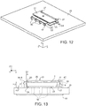
- Figures 12 and 13 show a configuration where the power device 1 is fixed to the substrate 20 with the leadframe 15 facing upwards (at a distance from the substrate 20), and heat sinkers are arranged both on top and underneath the power device 1.
- the expression “leadframe 15 facing upwards” indicates that the die-attach support 24C faces upwards (first base 2A of the package 2 facing downwards, towards the substrate 20, and second base 2B of the package 2 facing upwards) and the pins 14A and 14B as well as the bar 14C project downwards.
- a first heat sinker 22 is fixed to the second base 2B of the package 2 (on top of this) and a second heat sinker 23 is fixed to the first base 2A of the package 2, in the gap between the substrate 20 and the package 2.
- the first and second heat sinkers 22, 23 have here a thickness equal to the spacing distance H3. Furthermore, they may have any shape, for example a simple rectangular shape. In the embodiment shown, they have the same shape, generally a C shape, with a main portion 26 having a rectangular shape elongated in a direction parallel to the first Cartesian axis Y and a pair of legs 27 that extend from adjacent edges of a long side of the main portion 26, facing the bar 14C.
- the length of the heat sinkers 22, 23 (in the direction of the first Cartesian axis Y) is greater than the length L ( Figure 2 ) of the package 2, and the legs 27 extend outside the package 2, alongside and at a distance from the bar 14C.
- the heat sinkers 22, 23 are further arranged vertically on top of each other.
- a vertical wall 29 (represented with a dashed line in Figure 13 ) in thermal contact with the first and second heat sinkers 22, 23, and possibly with the drain lead 4C, but insulated with respect to the gate and source leads 4A, 4B, in order to respect the creepage distance.
- the vertical wall 29 extends alongside the power device 1, facing the bar 14C, with main extension parallel to the third plane YZ of the Cartesian coordinate system (thus, perpendicular to the substrate 20).
- the first and second heat sinkers 22, 23 are made of conductive material, typically metal such as copper or aluminium; further, the heat sinkers 22, 23 preferably have a thickness equal to the spacing distance H3.
- the main portion 26 of the second heat sinker 23 is arranged laterally between the projecting portions of the leads 4A-4C.
- main portion 26 is arranged vertically between the first base 2A of the package 2 and the substrate 20, physically in direct contact with them, and enables thermal dissipation of the power device 1 downwards.
- the substrate 20 may have connection vias 30, connecting the second heat sinker 23 to the dissipating lamina 31.
- the first heat sinker 22 is fixed to the second base 2B of the package 2, specifically to the die-attach support 24C. Since the die 6 (here not visible) lies directly on the die-attach support 24C, the first heat sinker 22 is not insulated from the die 6. Furthermore, in presence of the vertical wall 29 connecting the first heat sinker 22 to the second heat sinker 23, the latter is not electrically insulated from the die 6, either.
- the vertical wall 29 is arranged at a distance from the drain projection 8 of the bar 14C, even though this is not necessary in this case, since the vertical wall 29 is electrically connected to the drain pad 10C ( Figure 3 ) through the first heat sinker 22.
- the heat sinkers 22, 23, the vertical wall 29 (if present), and the dissipating lamina 31 (if present) form a heat-dissipation structure for the die 6.
- the power device 1 provides a high thermal dissipation.
- Figures 12-13 is designed so as to respect the creepage criteria as regards the first distance D1, between the first heat sinker 22 and the gate and source pins 14A, 14B ( Figure 12 ), a third distance D3, between the second heat sinker 23 and the gate and source pins 14A, 14B ( Figure 13 ), as well as a fourth distance D4 between the second heat sinker 23 and the bar 14C ( Figure 13 ).
- Figures 14-18 show a power device 35 having an inner dissipating lamina, insulated with respect to the die 6.
- the power device 35 has a base structure similar to that of the power device 1 shown in Figures 1-8 , so that parts that are similar are designated by the same reference numbers and will not be described any further.
- the power device 35 of Figures 14-18 (having equal below and lateral views as the power device 1 of Figures 3 and 4-6 so that these views are not represented again) comprises an insulating dissipative region 36 (also referred to as insulating clip), embedded in the package 2 and extending between the die 6 and the first base 2A of the package 2.
- insulating dissipative region 36 also referred to as insulating clip
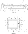
- the insulating dissipative region 36 is here a DCB (Direct Copper Bonding) substrate; namely, it is formed by a triple layer, including a first conductive layer 37, an intermediate insulating layer 38, and a second conductive layer 39, as may be seen in particular in Figure 16 .
- DCB Direct Copper Bonding
- the first conductive layer 37 has a top surface that extends flush with the first base 2A of the package 2 and occupies most part of the area of the first base 2A.
- the intermediate insulating layer 38 extends underneath the first conductive layer 37 and has a greater area than the first conductive layer 37.
- the second conductive layer 39 is bonded to the die 6 through a second adhesive layer 40, as explained in detail hereinafter.
- the first and second conductive layers 37, 39 are made of electrically and thermally conductive material, typically metal, such as copper.
- the intermediate insulating layer 38 may be of alumina (Al 2 O 3 ), which has excellent characteristics of electrical insulation, but is a good thermal conductor, so that the first base 2A of the package 2 is electrically insulated from the die 6, even at high voltages, but is thermally connected thereto.
- the second adhesive layer 40 is obtained, for example, from a conductive solder paste, patterned so as to form a first adhesive portion 40A and a second adhesive portion 40B.
- the first adhesive portion 40A extends between the second conductive layer 39 and the die 6 so as to be in direct contact with the source pad 10B ( Figure 8 ).
- the second adhesive portion 40B extends between the second conductive layer 39 and the inner portion 24B of the source leads 4B.
- the second conductive layer 39 of the insulating dissipative region 36 enables electrical contact between the source pad 10B (not visible in Figures 16-18 ) and the source leads 4B.
- the gate contact pad 10A is connected to the respective gate lead 4A via a bonding wire 11A, as may be seen in Figures 17 and 18 .
- the power device 35 of Figures 14-18 thus provides an even higher capacity of thermal dispersion, thanks to the presence of the insulating dissipative region 36.
- the power device 35 of Figures 14-18 may be mounted on a substrate, on both sides thereof, with the leadframe 15 facing upwards or downwards, may be coupled to external heat sinkers, as discussed above with reference to Figures 9-13 and described hereinafter, and may be stacked.
- Figure 19 shows a configuration where the power device 35 is bonded to the substrate 20, with the leadframe 15 facing downwards, the insulating dissipative region 36 facing upwards, and a heat sinker 45 arranged on top of the power device 35. Also in this case, as in Figure 9 , the pins 14A and 14B of the gate lead 4A and source leads 4B and the bar 14C of the gate lead 4C project upwards.
- the heat sinker 45 has the C shape described with reference to the first and second heat sinkers 22, 23 of Figure 12 , but could have the same rectangular shape as the heat sinker 21 of Figure 9 .
- the heat sinker 45 is in direct contact with the insulating dissipative region 36 and thus increases the dissipation capacity thereof.
- Figure 20 shows a configuration where the power device 35 is bonded to the substrate 20 with the leadframe 15 facing upwards, the insulating dissipative region 36 facing downwards (towards the substrate 20), and the heat sinkers arranged both on top of and underneath the power device 35, as in the configuration of Figure 12 .
- the first heat sinker 22 is bonded to, and in contact with, the die-attach support 24C and is thus arranged at the same voltage as the drain pad (10C in Figure 3 ).
- the second heat sinker 23 extends between the power device 35 and the support 20 in the gap due to the projecting leads 4A-4C (as described in detail with reference to Figures 12-13 ) and is in contact with the insulating dissipative region 36; the second heat sinker 23 is thus electrically insulated from the die 6.
- the heat sinkers 22, 23, the vertical wall 29 (if present) and the dissipating lamina 31 (if present) form a heat-dissipation structure for the die 6 (not visible).
- the power device 1 has a high thermal dissipation.
- the structure of Figures 19-20 in particular in presence of the vertical wall 29, whether in contact or not with the bar 14C, is designed, in any case, so as to respect the creepage criteria.
- Figures 21 and 22 show a power device 45 having an inner dissipating lamina, not insulated with respect to the die 6.
- the power device 45 has a basic structure similar to the power devices 1 and 35 shown in Figures 1-8 and 14-18, so that similar parts are designated by the same reference numbers and will not be described any further.
- the power device 45 of Figures 21-22 (having the same below and side views as the power device 1 of Figures 3 and 4-6 so that these views are not represented again) has the die 6 directly bonded to the leadframe 15 with its second face 6B (having the drain pad 10C, Figure 8 ) and comprises a conductive dissipative region 46 (also known as conductive clip) embedded in the package 2 except for a top surface, flush with the first base 2A of the package 2.
- the conductive dissipative region 46 is here formed as a single monolithic region, for example of copper, and extends between the first base 2A, on one side, and the die 6, on the other.
- the conductive dissipative region 46 is in contact with the source pad 10B ( Figure 8 ) through the first adhesive portion 40A (not visible in Figure 22 ) of the second adhesive layer 40 and with the inner portion 24B of the source leads 4B through the second adhesive portion 40B, as described with reference to Figure 16 for the second conductive layer 39.
- the conductive dissipative region 46 thus electrically connects the source pad 10B and the source leads 4B, like the second conductive layer 39 in Figure 18 .
- the conductive dissipative region 46 is laterally staggered with respect to the gate contact pad 10A ( Figure 8 ), analogously to the first insulating dissipative region 34 in Figure 18 .
- the gate contact pad 10A and the gate lead 4A are here in mutual electrical contact through a copper wire, as shown in Figures 17 and 18 .
- the conductive dissipative region 46 is in direct electrical and thermal contact with the source region (not shown) of the power device 45 and provides a high thermal dispersion both on the underside (second base 2B of the package 2) and on the upper side (first base 2A of the package 2).
- the conductive dissipative region 46 is not electrically insulated from the die 6.
- the distance between the conductive dissipative region 46 and the bar 14C is designed so as to satisfy the provided insulation conditions (creepage).
- the conductive dissipative region 46 is shaped so that its top surface has a width (in a direction parallel to the second Cartesian axis X, i.e., along the distance between the gate and source pins 14A, 14B and the bar 14C) that is greater at its base in contact with the die 6 than at its portion facing the first base 2A of the package 2.
- a fifth creepage distance D5 ( Figure 22 ) between the edge of the conductive dissipative region 46 (at the first base 2A of the package 2) and the bar 14C, as well as a sixth distance D6 between the edge of the die-attach support 24C and the base of the pins 14A, 14B of the gate lead 4A and source leads 4B are appropriate chosen.
- the conductive dissipative region 46 may have a length (parallel to the first Cartesian axis Y) approximately equal to the source pad 10B ( Figure 8 ) of the die 6.
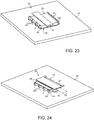
- the power device 45 of Figures 21-22 may be mounted on the substrate 20 with the leadframe 15 facing downwards (the leads 4A-4C projecting upwards), as shown in Figure 23 , or with the leadframe 15 facing upwards (the leads 4A-4C projecting downwards), as shown in Figure 24 .
- a heat sinker 41 is bonded to the first base 2A of the package 2, for example soldered or screwed to the insulating material thereof.
- the heat sinker 41 is in electrical and thermal contact with the conductive dissipative region 46 (not visible) and thus with the source pad 10B ( Figure 8 ).
- the creepage distance between the heat sinker 41 and the bar 14C (analogous to the second creepage distance D2 of Figure 9 , but much greater, due to the connection of the heat sinker 41 to the source pad 10B, Figure 8 ) is chosen using known criteria.
- a gap extends between the power device 45 and the substrate 20; a first heat sinker 42 is fixed to the second base 2B of the package 2 (on top thereof) and a second heat sinker 43 (having a rectangular shape) is bonded to the first base 2A of the package 2, in the gap between the substrate 20 and the package 2.
- first heat sinker 42 is in electrical and thermal contact with the drain pad 10C ( Figure 3 ), and the second heat sinker 43 is in electrical and thermal contact with the source pad 10B ( Figure 8 ).
- the creepage is here given by the distance of the first heat sinker 42 from the gate and source leads 4A, 4B (analogous to the third creepage distance D3 of Figure 12 ) and by the distance of the second heat sinker 43 from the bar 14C (seventh creepage distance D7), as well as by the distance between the two heat sinkers 42 and 43, which is equal to the thickness of the device 45.
- Figures 25 and 26 refer to a power device 55 with electrical insulation of both faces 2A, 2B of the die 6, which is electrically connected with the outside world only through the leads 4A-4C.
- the power device 55 (having same above view as the power device 35 of Figure 14 and same side views as the power device 1 shown in Figures 4-6 ) has the die-attach support 24C separate from the bar 14C, as visible in the view from below of Figure 25 and in the cross-section of the not packaged device of Figure 26 .
- the power device 55 has a similar structure to the power device 35 of Figures 14-18 , except for the separation of the die-attach support 24C, mentioned above, and for the presence of a second insulating dissipative region 56, in addition to the insulating dissipative region 36, hereinafter referred to, for clarity, as first insulating dissipative region 36.
- the second insulating dissipative region 56 has a structure similar to the first insulating dissipative region 36 and is here formed as a DCB substrate including a first conductive layer 57, an intermediate insulating layer 58, and a second conductive layer 59, formed as described in detail with reference to Figure 16 for the corresponding layers 37-39 of the first insulating dissipative region 36.
- the insulating dissipative region 56 could itself form, and thus replace, the die-attach support 24C.
- the first conductive layer 57 of the second insulating dissipative region 56 is bonded, in particular glued, to the second face 6B of the die 6 through a third adhesive layer 60, of a conductive type, for example a conductive solder paste.
- the second insulating dissipative region 56 (in particular, the first conductive layer 57 of the latter) and the third conductive adhesive layer 60 here have an area (in a plane parallel to the first plane XY of the Cartesian coordinate system) greater than the die 6 and laterally project beyond the die 6 (in the direction of the second Cartesian axis X) towards the bar 14C.
- the second conductive layer 59 of the second insulating dissipative region 56 is bonded to the die-attach support 24C. Consequently, in this embodiment, the die-attach support 24C is no longer electrically connected to the drain pad 10C ( Figure 8 ) of the power device 55.
- the drain lead 4C has here a bonding projection 34, extending from the bar 14C towards the inside of the package 2 and such as to partially overlap the first conductive layer 57 of the second insulating dissipative region 56.
- the bonding projection 34 is glued to the third conductive adhesive layer 60 at the projecting portion thereof.
- the drain pad 10C ( Figure 3 ) on the second face 6B of the die 6, the third conductive adhesive layer 60, and the drain lead 4C are in electrical connection; instead, the second face 2B of the power device 55 (formed by the die-attach support 24C) is electrically insulated from the die 6 by virtue of the intermediate insulating layer 58 of the second insulating dissipative region 56, and the second insulating dissipative region 56 provides a high thermal conductivity for the die.
- the die 2 is, however, thermally connected both upwards (first base 2A of the package 2), through the first insulating dissipative region 36 (the exposed top face 2A whereof is electrically insulated thanks to the first conductive layer 37), and downwards (second base 2B), through the second insulating dissipative region 56.
- the power device 55 of Figures 25 and 26 may be mounted in a way not represented with the leadframe 15 facing upwards or downwards, like the power device 35, as shown in Figures 19 and 20 .
- the vertical wall 29 that connects the first heat sinker 22 to the second heat sinker 23 also the latter will be electrically insulated, since it is only in contact with the first insulating dissipative region 36, insulated with respect to the die 2.
- the structure of Figures 19-20 in particular in presence of the vertical wall 29, whether in contact or not with the bar 14C, is designed so as to respect the creepage criteria.
- Figure 27 shows a parallel circuit arrangement 63 that may be implemented by stacking and parallel-connecting a plurality of power devices, designated as a whole by 65, each whereof may be formed by one of the power devices 1, 35 and 55 of Figures 1-20 and 24-25 .
- the stacked power devices 65 are all of the same type.
- the parallel circuit arrangement 63 of Figure 27 comprises a plurality of power devices 65 (three which are shown here), having mutually coupled gate terminals G, mutually coupled drain terminals D, and mutually coupled source terminals.
- the circuit arrangement 63 may be implemented as shown in Figures 28-30 .
- Figures 28-29 show a possibility of stacking the power devices 65 in a configuration with the leadframes 15 ( Figures 7 , 8 , 16-18 ) arranged facing upwards and the pins 14A, 14B and the bar 14C projecting downwards.
- the power devices 65 (which comprise a bottom power device 65', an intermediate power device 65", and a top power device 65'" and are designated by prime signs when necessary to distinguish them) form a stack 64, are vertically arranged on top of each other and bonded to the first face 20A of the substrate 20, with the gate pins 14A mutually aligned in the vertical direction (parallel to the third Cartesian axis Z) and in direct contact with each other (possibly with interposition of an adhesive, for example a solder paste, not shown), the source pins 14B mutually aligned and in direct contact with each other (possibly with interposition of an adhesive, for example a solder paste, not shown), and the bars 14C mutually aligned and in direct contact with each other (
- the pins 14A, 14B project downwards so that the package 2 of the bottom power device 65' is arranged at a distance from the substrate 20 by a gap 67 having a height equal to the spacing distance H3 ( Figure 4 ). Furthermore, the intermediate power device 65" and the top power device 65'" are arranged at a distance equal to the value of the gap 67 from the bottom power device 65' and from the intermediate power device 65", respectively.
- Heat sinkers 66 are arranged between the power devices 65, in the gaps 67, underneath the bottom power device 65' (where the heat sinker is designated by 66'), between the bottom power device 65' and the substrate 20, between the intermediate power device 65" and the top power device 65'", as well as above the top power device 65'".
- the heat sinkers 66 are similar to the first and second heat sinkers 22, 23, for example, of Figures 12, 13 , with legs 27 extending laterally (before and behind the plane of Figure 29 ) to the bars 14C and also mutually aligned.
- a first vertical wall 68 extends laterally to the power devices 65, throughout the height of the stack 64, in contact with the drain projections 8; a horizontal wall 69 extends over the stack 64 of power devices 65, in direct contact with the heat sinker 66 arranged at the top and with the top edge of the first vertical wall 68.
- the horizontal wall 69 has a width (in a direction parallel to the second Cartesian axis X) that is smaller than, and in any case does not exceed, the profile of the leadframe 15 of the underlying power device 65 and thus of the corresponding heat sinker 66 (which is aligned along the first Cartesian axis Y to the profile of the leadframe 15).
- the horizontal wall 69 has a length (in a direction parallel to the first Cartesian axis Y) greater than that of the power devices 65, as shown in Figure 29 , where the first vertical wall 68 is represented by a dashed line.
- the horizontal wall 69, the first vertical wall 68, the heat sinkers 66, and the column elements 71 are in direct contact with each other and form a dissipation structure 70 that surrounds the stack 64 of power devices 65.
- the dissipation structure 70 may further comprise further vertical walls, perpendicular to the first vertical wall 68, to increase further the dissipative capacity of the dissipation structure 70.
- Figure 29 shows a second vertical wall 72, represented with a dashed line and arranged on the right-hand side of the dissipation structure 70 (on the side close to the gate lead 4A), adjacent to and in contact with the heat sinkers 66.
- a third vertical wall 73 may be provided, also represented with a dashed line in Figure 29 , and arranged on the left-hand side of the dissipation structure 70, close to the source leads 4B, and also adjacent to and in contact with the heat sinkers 66.
- the vertical wall 68 extends at a distance from the drain projections 8, there is electrical connection between the drain leads 4C and the dissipation structure 70 only when the power devices 65 are made like the power devices 1 and 35 of Figures 1-8 and 14-18 .
- the dissipation structure 70 is electrically insulated from the drain leads 4C.
- the substrate 20 may comprise connection vias 30 and a dissipating lamina 31 fixed to the second face 20B of the substrate 20, as in Figures 10 and 11 .
- Figure 30 shows a possible implementation of the circuit arrangement of Figure 27 with the power devices 65 stacked in a configuration with the leadframes 15 ( Figures 7 , 8 , and 16-18 ) arranged facing downwards (towards the substrate 20) and with the pins 14A, 4B and the bar 14C projecting upwards.
- the power devices 65 are stacked on top of each other with the gate leads 4A, the source leads 4B, and the drain lead 4C in mutual contact, as described above with reference to Figures 28 and 29 , even though they are turned upside down, and the heat sinkers 66 (having, for example, the same shape as the first and second heat sinkers 22, 23 of Figures 9 and 19 ) extend between the bottom power device 65' and the intermediate power device 65", between the intermediate power device 65" and the top power device 65'", as well as above the top power device 65'".
- the bottom power device 65' is directly fixed to the substrate 20, as in the configurations of Figures 9 and 19 .
- Figure 31 shows a possible implementation of the circuit arrangement of Figure 27 with six power devices 65, arranged on both sides of the substrate 20.
- FIG. 31 In detail, in Figure 31 , three power devices 65 are stacked on top of each other to form a first stack 77 bonded to the first face 20A of the substrate 20, analogously to what described with reference to Figures 28 and 29 . Three other power devices 65 are stacked on top of each other to form a second stack 78, which is bonded to the second face 20B of the substrate 20 and has a specular structure with respect to the substrate 20. Consequently, the components of the second stack 78 are designated by the same reference numbers as those of the first stack 77.
- the power devices 65 are mounted in the configurations of Figures 12-13 and 20 , i.e., with the power devices 65 bonded to the substrate 20 with the leadframe 15 ( Figure 7 ) remote from the substrate 20 (upwards in the first stack 77 and downwards in the second stack 78) and the pins 14A and 14B and the bars 14C projecting towards the substrate 20 (downwards in the first stack 77 and upwards in the second stack 78).
- the substrate 20 has electrically conductive vias mutually connecting the power devices 65 of the two stacks 77 and 78.
- a first conductive via 79 passes right through the substrate 20 between the gate pin 14A of the bottom power device 65' of the first stack 77 and the gate pin 14A of the bottom power device 65' of the second stack 77, electrically connecting them together.
- Second conductive vias 80 extend through the substrate 20 between the source pins 14B of the bottom power device 65' of the first stack 77 and the source pins 14B of the bottom power device 65' of the second stack 77, electrically connecting them together.
- Third conductive vias 81 extend through the substrate 20 between the bar 14C of the bottom power device 65' of the first stack 77 and the bar 14C of the bottom power device 65' of the second stack 78, electrically connecting them together (it is noted that, in Figure 31 , the portion of the bars 14C of the bottom power transistors 65' projecting with respect to the first bases 2A is hidden by the legs 27 of the heat sinkers 66 - see for example Figure 12 ).
- the power devices 65 of each of the two stacks 77 and 78 are thus parallel-connected, as shown in Figures 29-29 . Further, the first, second, and third conductive vias 79-82 connect the two stacks 77 and 78 in parallel.
- the first, second, and third conductive vias 79-81 electrically connect the gate B, source S, and drain D terminals of the power devices 65, according to the electrical scheme of Figure 27 .
- fourth conductive vias 82 extend through the substrate 20 between the heat sinkers 66' of the stacks 77, 78 directly in contact with the substrate 20.
- the fourth conductive vias 82 connect thermally, but not electrically, the power devices 65 of the first and second stacks 77, 78.
- Figure 32 shows a different possible implementation of the circuit arrangement of Figure 27 for six power devices 65, on both sides of the substrate 20, arranged upside down with respect to Figure 31 .
- the power devices 65 are mounted so as to form a third stack 83 and a fourth stack 84, according to the configurations of Figures 9-11 and 19 , i.e., with the power devices 65 fixed to the substrate 20 with the leadframe 15 ( Figure 7 ) in a closer position to the substrate 20 (downwards in the third stack 83 and upwards in the fourth stack 84), with the pins 14A and 14B and the bars 14C projecting opposite to the substrate 20 (upwards in the third stack 83 and downwards in the fourth stack 84).
- the third and fourth stacks 83, 84 are similar to what described with reference to Figure 31 and are coupled to a respective dissipation structure, which has the same shape and arrangement as the dissipation structure 70 described above and is thus designated by the same reference number.
- first, second, and third conductive vias 79-81 extend through the substrate 20 for electrically coupling the gate and source pins 14A, 14B and the bars 14C.
- fourth conductive vias 82 extend through the substrate 20 and electrically and thermally couple the bottom devices 65' in contact with the substrate 20.
- the fourth conductive vias 82 provide anyway thermal-dissipation paths.
- first, second, and third conductive vias 79-81 contribute to the thermal dissipation.
- Figure 32 is similar to that of Figure 31 .
- Figure 33 shows a half-bridge circuit 85 that may be implemented by stacks of power devices 65, such as the power devices 55 of Figures 25-26 .
- the half-bridge circuit 85 comprises a first MOSFET 86 and a second MOSFET 87, series-connected between a first node and a second node at reference potentials 91, 92.
- An intermediate node 93 between the first and second MOSFETs 86, 87 forms an output terminal of the half-bridge circuit 85.
- the first MOSFET 86 has its drain terminal D coupled to the first node at reference potential 91, its source terminal S coupled to the intermediate node 93, and its gate terminal G coupled to a first control node 94.
- the second MOSFET 87 has its drain terminal D coupled to the intermediate node 93 and to the source terminal S of the first MOSFET 86, its source terminal S coupled to the second node at reference potential 92, and its gate terminal G coupled to a second control node 95.
- the first and second MOSFETs 86, 87 may be implemented by the third stack 83 and the fourth stack 84, respectively, of Figure 32 , where the third and fourth stacks 83, 84 are here connected as shown in Figure 34 and described hereinafter.
- the power devices 65 are made as described with reference to Figures 25-26 , so that the die-attach supports 24C ( Figure 26 ) of the power transistors 65 (and in particular the die-attach supports 24C of the bottom power transistors 65') are insulated with respect to the bars 14C.
- fifth conductive vias 96 extend through the substrate 20 between the first and second faces 20A, 20B of the substrate 20.
- the fifth conductive vias 96 extend between the source pins 14B of the bottom power transistor 65' of the third stack 83 and the bar 14C of the bottom power transistor 65' of the fourth stack 84 and connect them electrically together to form the intermediate node 93 of Figure 33 .
- one or more sixth conductive vias 97 extend through the substrate 20 (without intersecting the fifth conductive vias 96) and connect the power devices 65 of the third and fourth stacks 83, 84 thermally but not electrically, since the bottom bases 2B of the bottom power transistors 65' (in contact with the substrate 20) are insulated ( Figure 26 ).
- the power devices 1, 35, 45, 55 described herein have numerous advantages.
- the projecting configuration of the outer portions of the gate, source, and drain leads allows the power device to be arranged in two positions rotated through 180° about a horizontal axis, and to simply couple one or two heat sinkers 21, 22, 23, thus increasing the dissipation surface.
- the projecting portions of the gate, source, and drain leads 4A, 4B and 4C allow different power devices to be stably stacked (in particular in presence of the heat sinkers) and easily connected so as to increase the total electrical performance thereof (if they are connected in the parallel configuration shown in Figure 27 ) or to provide, for the power devices 55 of Figures 25-26 , more complex circuit configurations (such as the half-bridge arrangement shown in Figure 33 ), thus enabling a high thermal dissipation.
- the described power devices may be easily connected according to different circuit arrangements.
- the heat sinkers 21, 22 and 23 may have any shape.
- the heat sinker 21 of Figures 9-11 may be C-shaped, ensuring the creepage distance in the direction of the first Cartesian axis Y.
- the power devices of one stack may be rotated through 180° about a vertical axis (parallel to the third Cartesian axis Z) of the stacks 77, 78, or 83, 84, in particular for providing different circuit arrangements.
- a vertical dissipating structure similar to the first vertical wall 68 of Figure 30 may be arranged on the side the stack of source leads 4B in the stacks 77, 78, 83, 84 of Figures 31 , 32, and 34 , but arranged on the opposite side and in contact with only the three stacks of source pins 14B (and thus insulated with respect to the stack of gate pins 14A).
Landscapes
- Engineering & Computer Science (AREA)
- Microelectronics & Electronic Packaging (AREA)
- Manufacturing & Machinery (AREA)
- Lead Frames For Integrated Circuits (AREA)
- Cooling Or The Like Of Semiconductors Or Solid State Devices (AREA)
- Mounting Components In General For Electric Apparatus (AREA)
Abstract
Description
- The present invention relates to a packaged stackable electronic power device for surface mounting and to a circuit arrangement comprising a plurality of packaged electronic power devices, mutually stacked.
- For instance, the device may operate at high voltage (even up to 1700 V) with currents that may switch rapidly, such as silicon carbide or silicon devices, or example MOSFETs, superjunction MOSFETs, IGBTs, and the like, either in bridge (half-bridge or full-bridge) configuration or in A.C. switch configuration, PFC (Power-Factor Correction) circuits, SMPS (Switch-Mode Power Supply) devices.
- For such electronic power devices, particular packages have been devised, which enable a high heat dispersion. These packages are generally formed by rigid insulating bodies, for example of resin, having a parallelepipedal shape, embedding a die integrating the electronic component(s), as well as a dissipation structure arranged between the die, facing the package surface and generally occupying most of a major base of the parallelepipedal shape. The dissipation structure is sometimes formed by the supporting structure (referred to as "leadframe"), of metal, which carries the die and has a plurality of leads for external connection. In general, in this case, the leadframe has a surface directly facing the outside.
- For instance, in case of a packaged device comprising a MOSFET or an IGBT, the die integrating the MOSFET generally has a drain contact pad on an own first major surface and at least two contact pads (respectively, a source pad and a gate pad) on a second major surface, opposite to the first surface. A transistor contact pad (typically the drain pad) is fixed to the supporting portion of the leadframe. The other contact pads (typically, the gate and source pads) are coupled to the other leads by bonding wires or clips. This standard package normally envisages arrangement of the leads on the same side of the dissipation structure and thus normally enables dissipation downwards.
- The present applicant has further developed a package enabling cooling upwards, thanks to an appropriate configuration of the supporting portion of the leadframe and of the leads. In particular, this solution envisages a leadframe formed by a DBC (Direct-Bonded Copper) multilayer, which enables arrangement of two or more dice arranged side by side, each coupled, with its own drain pad, to a different portion, electrically insulated from the adjacent portions, of one of the conductive layers of the DBC supporting multilayer. Drain leads are fixed to the various portions of the conductive layer; the other contact pads (source and drain pads) are connected to leads of their own. This solution, allowing different circuit topologies and components to be formed, requires, however, a large area when many dice are provided, due to the side-by-side arrangement thereof.
- Italian patent application No.
102019000013743, filed on August 1, 2019 - The above solution, very effective for devices with bridge connection, is however somewhat complex in case of simpler circuits or when a high power is desired (and thus it is desired to dissipate high heat).
- The aim of the present invention is to provide a device that overcomes the limitations of the prior art.
- According to the present invention, a stackable, packaged electronic power device for surface mounting and a circuit arrangement are provided, as defined in the attached claims.
- For a better understanding of the present invention, some embodiments thereof are now described, purely by way of non-limiting example, with reference to the attached drawings, wherein:
-
Figure 1 is a perspective view of a packaged power device, according to the present disclosure; -
Figures 2-6 are, respectively, a top view, a bottom view, a front view, a left lateral view, and a right lateral view of the power device ofFigure 1 ; -
Figure 7 is a lateral view, partially phantom, of the power device ofFigure 1 ; -
Figure 7A shows a variant of the lateral view ofFigure 7 ; -
Figure 8 is a perspective view of the device ofFigure 1 , without package; -
Figure 9 is a perspective view of the power device ofFigure 1 mounted on a support, in a configuration; -
Figure 10 is a lateral view of the power device ofFigure 1 , mounted on a support and with a rear heat sinker; -
Figure 11 is a perspective, partially phantom view of the mounting configuration ofFigure 10 ; -
Figure 12 is a perspective view of the power device ofFigure 1 mounted on a support, in another configuration; -
Figure 13 is a lateral view of the mounted power device ofFigure 12 with a rear heat sinker; -
Figures 14 and 15 are, respectively, a perspective view and a bottom view of a packaged power device, according to a different embodiment; -
Figure 16 is a cross-section, taken along line XVI-XVI ofFigure 15 , of the power device ofFigures 14 and 15 , before packaging; -
Figures 17-18 are, respectively, a top plan view and a top perspective view of the power device ofFigures 14 and 15 , before packaging; -
Figure 19 is a perspective view of the power device ofFigures 14-18 mounted on a support, in a configuration; -
Figure 20 is a perspective view of the power device ofFigures 14-18 mounted on a support, in a different configuration; -
Figure 21 is a perspective view of a packaged power device, according to a different embodiment; -
Figure 22 is a cross-section, taken along line XXII-XXII ofFigure 21 , of the power device ofFigure 21 , with phantom parts; -
Figure 23 is a perspective view of the power device ofFigure 21 mounted on a heat-dissipation support, in a configuration; -
Figure 24 is a perspective view of the power device ofFigure 21 mounted on a support, in a different configuration; -
Figure 25 is a top plan view of a further embodiment of the present packaged power device; -
Figure 26 is a cross-section, taken along line XXVI-XXVI ofFigure 25 , of the power device ofFigure 25 , with ghost parts; -
Figure 27 shows an equivalent electrical diagram of a circuit arrangement obtainable by stacking the power devices ofFigures 1-20 and25-26 ; -
Figure 28 is a front view, similar toFigure 4 , of a stack of power devices mounted on a support, in a configuration for implementing the circuit arrangement ofFigure 27 ; -
Figure 29 is a left lateral view, similar toFigure 5 , of the stack of power devices ofFigure 28 ; -
Figure 30 is a front view, similar to thatFigure 4 , of a stack of power devices mounted on a support, in another configuration for implementing the circuit arrangement ofFigure 27 ; -
Figure 31 is a front view, similar toFigure 4 , of two stacks of power devices mounted on a support, for implementing a different circuit arrangement; -
Figure 32 is a front view, similar toFigure 31 , of a stack of power devices mounted on a support according to a different configuration; -
Figure 33 shows an equivalent electrical diagram of a different circuit arrangement obtainable by stacking the power devices ofFigures 25-26 ; and -
Figure 34 is a front view, similar toFigure 4 , of a stack of power devices of the type shown inFigures 25-26 mounted on a support, in a configuration for implementing the circuit arrangement ofFigure 33 . - In the following description, the spatial indications such as "above", "below", "at the top", "at the bottom", "overlying", "underlying", "on the left", "on the right" and the like refer to the represented figures and are to be understood only in a relative sense.
-
Figures 1-8 show apower device 1, such as a MOSFET, for example of silicon carbide or silicon, but the description below applies to devices of different types, such as superjunction MOSFETs, IGBTs and the like, and power circuits comprising such devices, for example circuits in bridge (half-bridge or full-bridge) configuration or in A.C. switch configuration, PFC (Power-Factor Correction) circuits, and SMPS (Switch-Mode Power Supply) devices. - The
power device 1 comprises apackage 2 of electrically insulating material, such as resin, embedding a die 6 (Figures 7 and8 ). The die 6 has afirst face 6A (at the top inFigure 7 ) and asecond face 6B (at the bottom inFigure 7 ) where contact pads are formed, in a known way, of whichFigure 8 shows schematically onlygate contact pads 10A andsource contact pads 10B. Thegate pads 10A andsource pads 10B are arranged on thefirst face 6A; adrain pad 10C, not visible and represented schematically with dashed line inFigure 3 , is arranged on thesecond face 6B. Thecontact pads 10A-10C are connected, in a known way described in greater detail hereinafter, to a supporting structure, so-called leadframe, designated as a whole by 15 (Figure 7 ), comprising leads (here designated by 4A-4C) in part embedded in thepackage 2 and in part projecting therefrom and configured to enable surface mounting. - In detail, the leads 4A-4C here form one
gate lead 4A, three source leads 4B, and onedrain lead 4C. - The
package 2 has a generally parallelepipedal shape, here slightly flared, having afirst base 2A (here represented at the top) parallel to a first plane XY of a Cartesian coordinate system, asecond base 2B, also parallel to the first plane XY, and fourlateral surfaces 2C-2F, extending transversely to the first plane XY. Since the first andsecond bases lateral surfaces 2C-2F of thepackage 2 also form the top and bottom faces as well as the lateral faces of the power device 1 (except for outer portions of the leads, as explained below), hereinafter, for simplicity, the faces of thepower device 1 will be designated by the same numbers as thebases lateral surfaces 2C-2F of thepackage 2 even when, in the embodiments shown and discussed hereinafter, the top and bottom faces of thepower device 1 are occupied in part by conductive structures and the outer portions of the leads extend on the lateral faces. - In the embodiment shown in
Figures 1-8 , thesecond base 2B has a slightly greater area than thefirst base 2A; the four lateral surfaces define a firstlateral surface 2C, a secondlateral surface 2D (opposite to the firstlateral surface 2C), a thirdlateral surface 2E, and a fourthlateral surface 2F (opposite to the thirdlateral surface 2E). Thegate lead 4A and the source leads 4B are arranged along the firstlateral surface 2C, at a uniform distance from each other (along a first Cartesian axis Y of the Cartesian coordinate system having further a second Cartesian axis X and a third Cartesian axis Z); thedrain lead 4C is arranged on the secondlateral surface 2D, as explained in detail hereinafter. - The
gate lead 4A and source leads 4B have respectiveouter portions pins package 2, andinner portions Figure 8 and embedded in thepackage 2. - Here, the
pins gate lead 4A and source leads 4B are formed by laminas, with a much smaller thickness than the other dimensions (and are thus substantially planar), have equal shapes, generally rectangular, and extend perpendicular to the firstlateral surface 2C (parallel to a second plane XZ of the Cartesian coordinate system). - The
pins gate lead 4A and source leads 4B have a greater height (in a direction parallel to a third Cartesian axis Z of the Cartesian coordinate system) than thepackage 2, with a first edge (the bottom edge inFigures 4-7 ) flush with thesecond face 2B of thepackage 2 and a second edge (the top edge inFigures 4-7 ) projecting with respect to thefirst face 2A of thepackage 2. - The
pins gate lead 4A and source leads 4B further each have a respective gate/source projection 7 facing the outside of the package 2 (see, in particular,Figures 4 and 7 ) . These projections may be useful for positioning tips of tester probes, during measurement. - The
inner portions Figure 8 ). - In detail, the
inner portion 24A of thegate lead 4A is formed by a thick lamina portion, having an approximately parallelepipedal shape, with bases parallel to the first plane XY and a width (in a direction parallel to the first Cartesian axis Y) greater than the respectiveouter portion 14A for enabling soldering of a firstelectrical bonding wire 11A to thegate contact pad 10A (Figure 8 ). - The
inner portion 24B of the source leads 4B is common, has an approximately parallelepipedal shape with bases parallel to the first plane XY, is elongated in a direction parallel to the first Cartesian axis Y, is rigid with, and electrically connected, to theouter portions 14B of all three source leads 4B. Theinner portion 24B of the source leads 4B is further electrically connected to thesource pad 10B through one ormore wires 11B (one whereof is shown inFigure 8 ). - As an alternative to wire
bonding 11B, as shown inFigure 7A , theinner portion 24B of the source leads 4B may be electrically connected to thesource pad 10B through a flat metal region orclip 17, parallelepiped-shaped, embedded in the resin of thepackage 2 that forms thefirst base 2A and that here extends between the metal region orclip 17 and thefirst base 2A. The flat metal region orclip 17 is fixed through anadhesive layer 18, for example a solder paste, as described in detail hereinafter with reference toFigure 16 (specifically with reference to the secondconductive layer 39, described there). - The drain lead 4C has an
outer portion 14C extending along the secondlateral surface 2D of thepackage 2 and abottom portion 24C facing thesecond base 2B of thepackage 2. - In detail, the
lateral portion 14C of the drain lead 4C is bar-shaped (and is consequently also referred to hereinafter asbar 14C), is contiguous with the secondlateral surface 2D of thepackage 2 and extends throughout the length thereof (on thefirst base 2A, designated by L inFigure 2 and measured parallel to the first Cartesian axis Y), approximately parallel to a third plane YZ of the Cartesian coordinate system. - The
bar 14C of the drain lead 4C has the same height (in the direction of the third Cartesian axis Z) as thepins gate lead 4A and source leads 4B and thus has a first edge (the bottom edge inFigures 4-7 ) flush with thesecond face 2B of thepackage 2 and a second edge (the top edge inFigures 4-7 ) projecting from thefirst face 2A of thepackage 2. - The
bar 14C of the drain lead 4C is further provided with adrain projection 8 facing the outside of the package 2 (see, in particular,Figures 4 and 7 ). - The
bottom portion 24C of the drain lead 4C forms a die-attach support (consequently hereinafter also referred to as die-attachsupport 24C and is also known as "die-attach pad") and is formed by a metal die with rectangular area, partially embedded in thepackage 2, so that its bottom (exposed) surface is flush with thesecond base 2B. In particular, the die-attachsupport 24C has a length (parallel to the first Cartesian axis Y) substantially equal to the length L of thebar 14C and extends (in the direction of a second Cartesian axis X of the Cartesian coordinate system) from thebar 14C as far as in proximity of theinner portions second base 2B of the package 2 (see alsoFigure 3 ), but at a safety distance from the gate and source leads 4A, 4B, taking into account operating parameters, such as the voltages foreseen during operation and possible other conditions, in a way known to the person skilled in the art, so as to respect the so-called creepage distance. - The die-attach
support 24C carries thedie 6, which is bonded to a top surface thereof via a firstadhesive layer 16, for example a conductive solder paste, which enables electrical contact between the drain pad (not shown, 10C inFigure 3 ) arranged on thesecond face 2B of thedie 6 and the die-attachsupport 24C, in a known way. - As already mentioned, the
pins gate lead 4A and source leads 4B and thebar 14C have the same height, are higher than thepackage 2 and project from thefirst base 2A thereof, as visible inFigures 4-6 . In particular, with reference toFigure 4 , if H1 is the height of thepackage 2, and H2 is the height of thegate lead 4A, source leads 4B and of thebar 14C, H2 > HI. Consequently, the distance between thefirst base 2A of thepackage 2 and the projecting edge of theouter portions 14A-14C of theleads 2A-2C is H3 = H2 -H1 (spacing distance). For instance, in one embodiment, thepackage 2 may have a height H1 of 2.3 mm, and thepins bar 14C may have a height H2 of 3-4.3 mm; thus, H3 may be 0.7-1 mm. - By virtue of the above characteristic, the
power device 1 may be mounted on a substrate, on both sides thereof, may be coupled to heat sinkers, and may be stacked, as discussed in detail hereinafter. - For instance,
Figure 9 shows a configuration where thepower device 1 is fixed to asubstrate 20, with theleadframe 15 facing downwards, and a heat sinker is arranged on top of thepower device 1. It is stressed that the expression "leadframe 15 facing downwards" indicates that the die-attachsupport 24C faces downwards, i.e., towards the substrate 20 (first base 2A facing upwards andsecond base 2B of thepackage 2 facing downwards) and thepins gate lead 4A and source leads 4B and thebar 14C project upwards. - The
substrate 20, for instance a printed-circuit board of FR4, is generally insulating, for example, of glass fibre with interposed conductive layers for connections, in a way known and not shown. In the configuration ofFigure 9 , theleads 4A-4C are fixed to thesubstrate 20 in a way not shown and in a per se known manner, for example through soldering to conductive paths (not shown). - A heat sinker (dissipation plate) 21 is fixed to the
first base 2A of thepackage 2, for example glued or screwed to thesubstrate 20 via supports not shown in the figure. - The
heat sinker 21 is formed by a lamina of conductive material, typically metal such as copper or aluminium. Theheat sinker 21 has, for example, a rectangular shape, with a length (parallel to the first Cartesian axis Y) greater than the length L of thebar 14C and of thepackage 2 and a width (parallel to the second Cartesian axis X) smaller than thepackage 2. Further, theheat sinker 21 is fixed at a distance from theleads 4A-4C; in particular, a first distance D1 (Figure 9 ) of theheat sinker 21 from thegate lead 4A and source leads 4B is appropriately chosen, in the direction of the second Cartesian axis X, taking into account operating parameters, such as the voltages foreseen during operation and other possible conditions, in a way known to the person skilled in the art (creepage distance). Likewise, a second distance D2 (Figure 9 ) between theheat sinker 21 and thebar 14C is chosen in the design stage so as to satisfy creepage criteria, if necessary. - The
heat sinker 21 further has, for example, a thickness equal to the spacing distance H3, even though in this configuration the thickness is not critical. - The
heat sinker 21 is thus physically in direct contact with thefirst base 2A of thepackage 2 and enables thermal dissipation of thepower device 1 upwards. - To increase thermal dissipation of the
power device 1, it is possible to thermally couple it to a dissipating lamina arranged on an opposite side of thesubstrate 20, so as to obtain dissipation also downwards, as shown in the configuration ofFigures 10 and 11 . - In
Figures 10 and 11 , thesubstrate 20, also here, for example, a printed-circuit board, has afirst face 20A and asecond face 20B. Thepower device 1 is fixed to thefirst face 20A of thesubstrate 20, possibly through an adhesive layer, such as a solder paste, not shown.Connection vias 30, for example of metal, such as copper, extend through thesubstrate 20, and are thermally and electrically conductive. The connection vias 30, represented dashed inFigure 10 , extend between the first andsecond faces substrate 2 and are in physical contact with thesecond base 2B of the package 2 (possibly through the adhesive layer, not shown), on thefirst face 20A, and thus with thedrain pad 10C (Figure 3 ), and with a dissipatinglamina 31 extending on thesecond face 20B of thesubstrate 20. - The dissipating
lamina 31 may have any shape, with a generally greater area than thepower device 1 to provide a high thermal dissipation. To this end, the dissipatinglamina 31 is made of thermally conductive material, for example a metal such as copper. Consequently, in this configuration, the dissipatinglamina 31 is in electrical contact with thedrain pad 10C (Figure 3 ) of thepower device 1. - The configuration of
Figures 10 and 11 thus provides an increased dissipation as compared to the configuration ofFigure 9 . -
Figures 12 and 13 show a configuration where thepower device 1 is fixed to thesubstrate 20 with theleadframe 15 facing upwards (at a distance from the substrate 20), and heat sinkers are arranged both on top and underneath thepower device 1. - It should be noted that the expression "
leadframe 15 facing upwards" indicates that the die-attachsupport 24C faces upwards (first base 2A of thepackage 2 facing downwards, towards thesubstrate 20, andsecond base 2B of thepackage 2 facing upwards) and thepins bar 14C project downwards. - In this way, in the configuration of
Figures 12-13 , thepackage 2 of thepower device 1 is raised with respect to thesubstrate 20 by the spacing distance H3. - In the configuration of
Figures 12-13 , afirst heat sinker 22 is fixed to thesecond base 2B of the package 2 (on top of this) and asecond heat sinker 23 is fixed to thefirst base 2A of thepackage 2, in the gap between thesubstrate 20 and thepackage 2. - The first and
second heat sinkers main portion 26 having a rectangular shape elongated in a direction parallel to the first Cartesian axis Y and a pair oflegs 27 that extend from adjacent edges of a long side of themain portion 26, facing thebar 14C. The length of theheat sinkers 22, 23 (in the direction of the first Cartesian axis Y) is greater than the length L (Figure 2 ) of thepackage 2, and thelegs 27 extend outside thepackage 2, alongside and at a distance from thebar 14C. The heat sinkers 22, 23 are further arranged vertically on top of each other. - As discussed in detail hereinafter, it is thus possible to arrange, if so desired, a vertical wall 29 (represented with a dashed line in
Figure 13 ) in thermal contact with the first andsecond heat sinkers - In
Figure 13 , thevertical wall 29 extends alongside thepower device 1, facing thebar 14C, with main extension parallel to the third plane YZ of the Cartesian coordinate system (thus, perpendicular to the substrate 20). - The first and
second heat sinkers 22, 23 (and thevertical wall 29, if present) are made of conductive material, typically metal such as copper or aluminium; further, theheat sinkers - Consequently, the
main portion 26 of thesecond heat sinker 23 is arranged laterally between the projecting portions of theleads 4A-4C. - In addition, the
main portion 26 is arranged vertically between thefirst base 2A of thepackage 2 and thesubstrate 20, physically in direct contact with them, and enables thermal dissipation of thepower device 1 downwards. - Also in this case, the
substrate 20 may haveconnection vias 30, connecting thesecond heat sinker 23 to the dissipatinglamina 31. - The
first heat sinker 22, as mentioned, is fixed to thesecond base 2B of thepackage 2, specifically to the die-attachsupport 24C. Since the die 6 (here not visible) lies directly on the die-attachsupport 24C, thefirst heat sinker 22 is not insulated from thedie 6. Furthermore, in presence of thevertical wall 29 connecting thefirst heat sinker 22 to thesecond heat sinker 23, the latter is not electrically insulated from thedie 6, either. - It is noted that, in
Figure 13 , thevertical wall 29 is arranged at a distance from thedrain projection 8 of thebar 14C, even though this is not necessary in this case, since thevertical wall 29 is electrically connected to thedrain pad 10C (Figure 3 ) through thefirst heat sinker 22. - In practice, the
heat sinkers die 6. In this way, in the configuration ofFigures 12 and 13 , thepower device 1 provides a high thermal dissipation. - Also the structure of
Figures 12-13 is designed so as to respect the creepage criteria as regards the first distance D1, between thefirst heat sinker 22 and the gate and source pins 14A, 14B (Figure 12 ), a third distance D3, between thesecond heat sinker 23 and the gate and source pins 14A, 14B (Figure 13 ), as well as a fourth distance D4 between thesecond heat sinker 23 and thebar 14C (Figure 13 ). -
Figures 14-18 show apower device 35 having an inner dissipating lamina, insulated with respect to thedie 6. - The
power device 35 has a base structure similar to that of thepower device 1 shown inFigures 1-8 , so that parts that are similar are designated by the same reference numbers and will not be described any further. - The
power device 35 ofFigures 14-18 (having equal below and lateral views as thepower device 1 ofFigures 3 and4-6 so that these views are not represented again) comprises an insulating dissipative region 36 (also referred to as insulating clip), embedded in thepackage 2 and extending between thedie 6 and thefirst base 2A of thepackage 2. - The insulating
dissipative region 36 is here a DCB (Direct Copper Bonding) substrate; namely, it is formed by a triple layer, including a firstconductive layer 37, an intermediate insulatinglayer 38, and a secondconductive layer 39, as may be seen in particular inFigure 16 . - Here, the first
conductive layer 37 has a top surface that extends flush with thefirst base 2A of thepackage 2 and occupies most part of the area of thefirst base 2A. The intermediate insulatinglayer 38 extends underneath the firstconductive layer 37 and has a greater area than the firstconductive layer 37. The secondconductive layer 39 is bonded to thedie 6 through a secondadhesive layer 40, as explained in detail hereinafter. - The first and second
conductive layers layer 38 may be of alumina (Al2O3), which has excellent characteristics of electrical insulation, but is a good thermal conductor, so that thefirst base 2A of thepackage 2 is electrically insulated from thedie 6, even at high voltages, but is thermally connected thereto. - The second
adhesive layer 40 is obtained, for example, from a conductive solder paste, patterned so as to form a firstadhesive portion 40A and a secondadhesive portion 40B. The firstadhesive portion 40A extends between the secondconductive layer 39 and thedie 6 so as to be in direct contact with thesource pad 10B (Figure 8 ). The secondadhesive portion 40B extends between the secondconductive layer 39 and theinner portion 24B of the source leads 4B. In practice, in this embodiment, the secondconductive layer 39 of the insulatingdissipative region 36 enables electrical contact between thesource pad 10B (not visible inFigures 16-18 ) and the source leads 4B. - Also in this embodiment, the
gate contact pad 10A is connected to therespective gate lead 4A via abonding wire 11A, as may be seen inFigures 17 and18 . - The
power device 35 ofFigures 14-18 thus provides an even higher capacity of thermal dispersion, thanks to the presence of the insulatingdissipative region 36. - The
power device 35 ofFigures 14-18 may be mounted on a substrate, on both sides thereof, with theleadframe 15 facing upwards or downwards, may be coupled to external heat sinkers, as discussed above with reference toFigures 9-13 and described hereinafter, and may be stacked. - In particular,
Figure 19 shows a configuration where thepower device 35 is bonded to thesubstrate 20, with theleadframe 15 facing downwards, the insulatingdissipative region 36 facing upwards, and aheat sinker 45 arranged on top of thepower device 35. Also in this case, as inFigure 9 , thepins gate lead 4A and source leads 4B and thebar 14C of the gate lead 4C project upwards. - In this case, the
heat sinker 45 has the C shape described with reference to the first andsecond heat sinkers Figure 12 , but could have the same rectangular shape as theheat sinker 21 ofFigure 9 . - In
Figure 19 , theheat sinker 45 is in direct contact with the insulatingdissipative region 36 and thus increases the dissipation capacity thereof. -
Figure 20 shows a configuration where thepower device 35 is bonded to thesubstrate 20 with theleadframe 15 facing upwards, the insulatingdissipative region 36 facing downwards (towards the substrate 20), and the heat sinkers arranged both on top of and underneath thepower device 35, as in the configuration ofFigure 12 . - In particular, in
Figure 20 , thefirst heat sinker 22 is bonded to, and in contact with, the die-attachsupport 24C and is thus arranged at the same voltage as the drain pad (10C inFigure 3 ). Thesecond heat sinker 23 extends between thepower device 35 and thesupport 20 in the gap due to the projecting leads 4A-4C (as described in detail with reference toFigures 12-13 ) and is in contact with the insulatingdissipative region 36; thesecond heat sinker 23 is thus electrically insulated from thedie 6. Also in this case, theheat sinkers Figures 19 and 20 , thepower device 1 has a high thermal dissipation. Also the structure ofFigures 19-20 , in particular in presence of thevertical wall 29, whether in contact or not with thebar 14C, is designed, in any case, so as to respect the creepage criteria. -
Figures 21 and 22 show apower device 45 having an inner dissipating lamina, not insulated with respect to thedie 6. - In particular, the
power device 45 has a basic structure similar to thepower devices Figures 1-8 and 14-18, so that similar parts are designated by the same reference numbers and will not be described any further. - The
power device 45 ofFigures 21-22 (having the same below and side views as thepower device 1 ofFigures 3 and4-6 so that these views are not represented again) has thedie 6 directly bonded to theleadframe 15 with itssecond face 6B (having thedrain pad 10C,Figure 8 ) and comprises a conductive dissipative region 46 (also known as conductive clip) embedded in thepackage 2 except for a top surface, flush with thefirst base 2A of thepackage 2. - The
conductive dissipative region 46 is here formed as a single monolithic region, for example of copper, and extends between thefirst base 2A, on one side, and thedie 6, on the other. Theconductive dissipative region 46 is in contact with thesource pad 10B (Figure 8 ) through the firstadhesive portion 40A (not visible inFigure 22 ) of the secondadhesive layer 40 and with theinner portion 24B of the source leads 4B through the secondadhesive portion 40B, as described with reference toFigure 16 for the secondconductive layer 39. Theconductive dissipative region 46 thus electrically connects thesource pad 10B and the source leads 4B, like the secondconductive layer 39 inFigure 18 . In addition, also here, theconductive dissipative region 46 is laterally staggered with respect to thegate contact pad 10A (Figure 8 ), analogously to the first insulatingdissipative region 34 inFigure 18 . In a way not visible, thegate contact pad 10A and thegate lead 4A are here in mutual electrical contact through a copper wire, as shown inFigures 17 and18 . - Consequently, in this embodiment, the
conductive dissipative region 46 is in direct electrical and thermal contact with the source region (not shown) of thepower device 45 and provides a high thermal dispersion both on the underside (second base 2B of the package 2) and on the upper side (first base 2A of the package 2). - However, the
conductive dissipative region 46 is not electrically insulated from thedie 6. Thus, during sizing, the distance between theconductive dissipative region 46 and thebar 14C is designed so as to satisfy the provided insulation conditions (creepage). - To this end, in the embodiment shown in
Figures 21-22 , theconductive dissipative region 46 is shaped so that its top surface has a width (in a direction parallel to the second Cartesian axis X, i.e., along the distance between the gate and source pins 14A, 14B and thebar 14C) that is greater at its base in contact with thedie 6 than at its portion facing thefirst base 2A of thepackage 2. - In particular, with this conformation, in the design stage, a fifth creepage distance D5 (
Figure 22 ) between the edge of the conductive dissipative region 46 (at thefirst base 2A of the package 2) and thebar 14C, as well as a sixth distance D6 between the edge of the die-attachsupport 24C and the base of thepins gate lead 4A and source leads 4B are appropriate chosen. - The
conductive dissipative region 46 may have a length (parallel to the first Cartesian axis Y) approximately equal to thesource pad 10B (Figure 8 ) of thedie 6. - The
power device 45 ofFigures 21-22 may be mounted on thesubstrate 20 with theleadframe 15 facing downwards (theleads 4A-4C projecting upwards), as shown inFigure 23 , or with theleadframe 15 facing upwards (theleads 4A-4C projecting downwards), as shown inFigure 24 . - In
Figure 23 , as shown inFigure 9 , aheat sinker 41 is bonded to thefirst base 2A of thepackage 2, for example soldered or screwed to the insulating material thereof. - Here, the
heat sinker 41 is in electrical and thermal contact with the conductive dissipative region 46 (not visible) and thus with thesource pad 10B (Figure 8 ). - In this way, a dual-face cooling is obtained as a result of the heat sinker 41 (arranged at the top) and the contact between the leadframe 15 (not visible in
Figure 23 ) and the back of thesubstrate 20, where a dissipating lamina 31 (Figure 10 ) may be arranged, thermally and electrically coupled throughconnection vias 30, as shown inFigure 10 . - Here, in the design stage, the creepage distance between the
heat sinker 41 and thebar 14C (analogous to the second creepage distance D2 ofFigure 9 , but much greater, due to the connection of theheat sinker 41 to thesource pad 10B,Figure 8 ) is chosen using known criteria. - In
Figure 24 , as inFigure 12 , a gap extends between thepower device 45 and thesubstrate 20; afirst heat sinker 42 is fixed to thesecond base 2B of the package 2 (on top thereof) and a second heat sinker 43 (having a rectangular shape) is bonded to thefirst base 2A of thepackage 2, in the gap between thesubstrate 20 and thepackage 2. - Here, the
first heat sinker 42 is in electrical and thermal contact with thedrain pad 10C (Figure 3 ), and thesecond heat sinker 43 is in electrical and thermal contact with thesource pad 10B (Figure 8 ). - Also here, a double-face cooling is obtained.
- The creepage is here given by the distance of the
first heat sinker 42 from the gate and source leads 4A, 4B (analogous to the third creepage distance D3 ofFigure 12 ) and by the distance of thesecond heat sinker 43 from thebar 14C (seventh creepage distance D7), as well as by the distance between the twoheat sinkers device 45. -
Figures 25 and 26 refer to apower device 55 with electrical insulation of bothfaces die 6, which is electrically connected with the outside world only through theleads 4A-4C. - In detail, the power device 55 (having same above view as the
power device 35 ofFigure 14 and same side views as thepower device 1 shown inFigures 4-6 ) has the die-attachsupport 24C separate from thebar 14C, as visible in the view from below ofFigure 25 and in the cross-section of the not packaged device ofFigure 26 . - In detail, the
power device 55 has a similar structure to thepower device 35 ofFigures 14-18 , except for the separation of the die-attachsupport 24C, mentioned above, and for the presence of a second insulatingdissipative region 56, in addition to the insulatingdissipative region 36, hereinafter referred to, for clarity, as first insulatingdissipative region 36. - The second
insulating dissipative region 56 has a structure similar to the first insulatingdissipative region 36 and is here formed as a DCB substrate including a firstconductive layer 57, an intermediate insulatinglayer 58, and a secondconductive layer 59, formed as described in detail with reference toFigure 16 for the corresponding layers 37-39 of the first insulatingdissipative region 36. - In a variant not shown, the insulating
dissipative region 56 could itself form, and thus replace, the die-attachsupport 24C. - In the embodiment of
Figures 25-26 , the firstconductive layer 57 of the second insulatingdissipative region 56 is bonded, in particular glued, to thesecond face 6B of thedie 6 through a thirdadhesive layer 60, of a conductive type, for example a conductive solder paste. The second insulating dissipative region 56 (in particular, the firstconductive layer 57 of the latter) and the third conductiveadhesive layer 60 here have an area (in a plane parallel to the first plane XY of the Cartesian coordinate system) greater than thedie 6 and laterally project beyond the die 6 (in the direction of the second Cartesian axis X) towards thebar 14C. The secondconductive layer 59 of the second insulatingdissipative region 56 is bonded to the die-attachsupport 24C. Consequently, in this embodiment, the die-attachsupport 24C is no longer electrically connected to thedrain pad 10C (Figure 8 ) of thepower device 55. - The drain lead 4C has here a
bonding projection 34, extending from thebar 14C towards the inside of thepackage 2 and such as to partially overlap the firstconductive layer 57 of the second insulatingdissipative region 56. Thebonding projection 34 is glued to the third conductiveadhesive layer 60 at the projecting portion thereof. - In this way, the
drain pad 10C (Figure 3 ) on thesecond face 6B of thedie 6, the third conductiveadhesive layer 60, and the drain lead 4C are in electrical connection; instead, thesecond face 2B of the power device 55 (formed by the die-attachsupport 24C) is electrically insulated from thedie 6 by virtue of the intermediate insulatinglayer 58 of the second insulatingdissipative region 56, and the second insulatingdissipative region 56 provides a high thermal conductivity for the die. - The
die 2 is, however, thermally connected both upwards (first base 2A of the package 2), through the first insulating dissipative region 36 (the exposedtop face 2A whereof is electrically insulated thanks to the first conductive layer 37), and downwards (second base 2B), through the second insulatingdissipative region 56. - The
power device 55 ofFigures 25 and 26 may be mounted in a way not represented with theleadframe 15 facing upwards or downwards, like thepower device 35, as shown inFigures 19 and 20 . - However, in this case, the
first heat sinker 22, fixed to thesecond base 2B of thepackage 2, and specifically to the die-attachsupport 24C, is insulated with respect to thedie 6, which does not lie directly on the die-attachsupport 24C. Even in the presence of thevertical wall 29 that connects thefirst heat sinker 22 to thesecond heat sinker 23, also the latter will be electrically insulated, since it is only in contact with the first insulatingdissipative region 36, insulated with respect to thedie 2. Also the structure ofFigures 19-20 , in particular in presence of thevertical wall 29, whether in contact or not with thebar 14C, is designed so as to respect the creepage criteria. -
Figure 27 shows aparallel circuit arrangement 63 that may be implemented by stacking and parallel-connecting a plurality of power devices, designated as a whole by 65, each whereof may be formed by one of thepower devices Figures 1-20 and24-25 . Preferably, the stackedpower devices 65 are all of the same type. - In detail, the
parallel circuit arrangement 63 ofFigure 27 comprises a plurality of power devices 65 (three which are shown here), having mutually coupled gate terminals G, mutually coupled drain terminals D, and mutually coupled source terminals. - The
circuit arrangement 63 may be implemented as shown inFigures 28-30 . -
Figures 28-29 show a possibility of stacking thepower devices 65 in a configuration with the leadframes 15 (Figures 7 ,8 ,16-18 ) arranged facing upwards and thepins bar 14C projecting downwards. The power devices 65 (which comprise abottom power device 65', anintermediate power device 65", and atop power device 65'" and are designated by prime signs when necessary to distinguish them) form astack 64, are vertically arranged on top of each other and bonded to thefirst face 20A of thesubstrate 20, with the gate pins 14A mutually aligned in the vertical direction (parallel to the third Cartesian axis Z) and in direct contact with each other (possibly with interposition of an adhesive, for example a solder paste, not shown), the source pins 14B mutually aligned and in direct contact with each other (possibly with interposition of an adhesive, for example a solder paste, not shown), and thebars 14C mutually aligned and in direct contact with each other (possibly with interposition of an adhesive, for example a solder paste, not shown). - Thanks to the mutual contact of the gate pins 14A, source pins 14B, and bars 14C of the
power devices 65, these are parallel-connected as represented inFigure 27 . - Here, the
pins package 2 of thebottom power device 65' is arranged at a distance from thesubstrate 20 by agap 67 having a height equal to the spacing distance H3 (Figure 4 ). Furthermore, theintermediate power device 65" and thetop power device 65'" are arranged at a distance equal to the value of thegap 67 from thebottom power device 65' and from theintermediate power device 65", respectively. -
Heat sinkers 66 are arranged between thepower devices 65, in thegaps 67, underneath thebottom power device 65' (where the heat sinker is designated by 66'), between thebottom power device 65' and thesubstrate 20, between theintermediate power device 65" and thetop power device 65'", as well as above thetop power device 65'". The heat sinkers 66 are similar to the first andsecond heat sinkers Figures 12, 13 , withlegs 27 extending laterally (before and behind the plane ofFigure 29 ) to thebars 14C and also mutually aligned. - A first
vertical wall 68 extends laterally to thepower devices 65, throughout the height of thestack 64, in contact with thedrain projections 8; ahorizontal wall 69 extends over thestack 64 ofpower devices 65, in direct contact with theheat sinker 66 arranged at the top and with the top edge of the firstvertical wall 68. - In order to respect the creepage distances, the
horizontal wall 69 has a width (in a direction parallel to the second Cartesian axis X) that is smaller than, and in any case does not exceed, the profile of theleadframe 15 of theunderlying power device 65 and thus of the corresponding heat sinker 66 (which is aligned along the first Cartesian axis Y to the profile of the leadframe 15). In addition, thehorizontal wall 69 has a length (in a direction parallel to the first Cartesian axis Y) greater than that of thepower devices 65, as shown inFigure 29 , where the firstvertical wall 68 is represented by a dashed line. -
Column elements 71 extend above thehorizontal wall 69, in contact therewith to increase the dissipative surface. - The
horizontal wall 69, the firstvertical wall 68, theheat sinkers 66, and thecolumn elements 71 are in direct contact with each other and form adissipation structure 70 that surrounds thestack 64 ofpower devices 65. - The
dissipation structure 70 may further comprise further vertical walls, perpendicular to the firstvertical wall 68, to increase further the dissipative capacity of thedissipation structure 70. For instance,Figure 29 shows a secondvertical wall 72, represented with a dashed line and arranged on the right-hand side of the dissipation structure 70 (on the side close to thegate lead 4A), adjacent to and in contact with theheat sinkers 66. Possibly, a thirdvertical wall 73 may be provided, also represented with a dashed line inFigure 29 , and arranged on the left-hand side of thedissipation structure 70, close to the source leads 4B, and also adjacent to and in contact with theheat sinkers 66. - In addition, in the arrangement shown, where the
drain projections 8 are in contact with thevertical wall 68, there is thermal and electrical continuity between the drain leads 4C and thedissipation structure 70. - If the
vertical wall 68 extends at a distance from thedrain projections 8, there is electrical connection between the drain leads 4C and thedissipation structure 70 only when thepower devices 65 are made like thepower devices Figures 1-8 and14-18 . - When the
power devices 65 are made like thepower devices 55 ofFigures 25 and 26 and thevertical wall 68 is arranged at a distance from thedrain projections 8, thedissipation structure 70 is electrically insulated from the drain leads 4C. Also in the embodiment ofFigures 28-29 , as represented with dashed lines inFigure 29 , thesubstrate 20 may compriseconnection vias 30 and a dissipatinglamina 31 fixed to thesecond face 20B of thesubstrate 20, as inFigures 10 and 11 . -
Figure 30 shows a possible implementation of the circuit arrangement ofFigure 27 with thepower devices 65 stacked in a configuration with the leadframes 15 (Figures 7 ,8 , and16-18 ) arranged facing downwards (towards the substrate 20) and with thepins bar 14C projecting upwards. - Here, the
power devices 65 are stacked on top of each other with the gate leads 4A, the source leads 4B, and the drain lead 4C in mutual contact, as described above with reference toFigures 28 and 29 , even though they are turned upside down, and the heat sinkers 66 (having, for example, the same shape as the first andsecond heat sinkers Figures 9 and19 ) extend between thebottom power device 65' and theintermediate power device 65", between theintermediate power device 65" and thetop power device 65'", as well as above thetop power device 65'". Thebottom power device 65' is directly fixed to thesubstrate 20, as in the configurations ofFigures 9 and19 . -
Figure 31 shows a possible implementation of the circuit arrangement ofFigure 27 with sixpower devices 65, arranged on both sides of thesubstrate 20. - In detail, in
Figure 31 , threepower devices 65 are stacked on top of each other to form afirst stack 77 bonded to thefirst face 20A of thesubstrate 20, analogously to what described with reference toFigures 28 and 29 . Threeother power devices 65 are stacked on top of each other to form asecond stack 78, which is bonded to thesecond face 20B of thesubstrate 20 and has a specular structure with respect to thesubstrate 20. Consequently, the components of thesecond stack 78 are designated by the same reference numbers as those of thefirst stack 77. - In both of the
stacks power devices 65 are mounted in the configurations ofFigures 12-13 and20 , i.e., with thepower devices 65 bonded to thesubstrate 20 with the leadframe 15 (Figure 7 ) remote from the substrate 20 (upwards in thefirst stack 77 and downwards in the second stack 78) and thepins bars 14C projecting towards the substrate 20 (downwards in thefirst stack 77 and upwards in the second stack 78). - The
substrate 20 has electrically conductive vias mutually connecting thepower devices 65 of the twostacks - In detail, a first conductive via 79 passes right through the
substrate 20 between thegate pin 14A of thebottom power device 65' of thefirst stack 77 and thegate pin 14A of thebottom power device 65' of thesecond stack 77, electrically connecting them together. - Second conductive vias 80 (hidden from the first via 79 in
Figure 31 , aligned thereto in a direction parallel to the first Cartesian axis Y) extend through thesubstrate 20 between the source pins 14B of thebottom power device 65' of thefirst stack 77 and the source pins 14B of thebottom power device 65' of thesecond stack 77, electrically connecting them together. - Third
conductive vias 81 extend through thesubstrate 20 between thebar 14C of thebottom power device 65' of thefirst stack 77 and thebar 14C of thebottom power device 65' of thesecond stack 78, electrically connecting them together (it is noted that, inFigure 31 , the portion of thebars 14C of thebottom power transistors 65' projecting with respect to thefirst bases 2A is hidden by thelegs 27 of the heat sinkers 66 - see for exampleFigure 12 ). - The
power devices 65 of each of the twostacks Figures 29-29 . Further, the first, second, and third conductive vias 79-82 connect the twostacks - In practice, in this configuration with six
power devices 65, the first, second, and third conductive vias 79-81 electrically connect the gate B, source S, and drain D terminals of thepower devices 65, according to the electrical scheme ofFigure 27 . - In
Figure 31 , fourthconductive vias 82 extend through thesubstrate 20 between the heat sinkers 66' of thestacks substrate 20. The fourthconductive vias 82 connect thermally, but not electrically, thepower devices 65 of the first andsecond stacks -
Figure 32 shows a different possible implementation of the circuit arrangement ofFigure 27 for sixpower devices 65, on both sides of thesubstrate 20, arranged upside down with respect toFigure 31 . - In detail, in
Figure 32 , thepower devices 65 are mounted so as to form athird stack 83 and afourth stack 84, according to the configurations ofFigures 9-11 and19 , i.e., with thepower devices 65 fixed to thesubstrate 20 with the leadframe 15 (Figure 7 ) in a closer position to the substrate 20 (downwards in thethird stack 83 and upwards in the fourth stack 84), with thepins bars 14C projecting opposite to the substrate 20 (upwards in thethird stack 83 and downwards in the fourth stack 84). - Apart from the orientation, the third and
fourth stacks Figure 31 and are coupled to a respective dissipation structure, which has the same shape and arrangement as thedissipation structure 70 described above and is thus designated by the same reference number. - In addition, the first, second, and third conductive vias 79-81 extend through the
substrate 20 for electrically coupling the gate and source pins 14A, 14B and thebars 14C. Also here, the fourthconductive vias 82 extend through thesubstrate 20 and electrically and thermally couple thebottom devices 65' in contact with thesubstrate 20. - With the configuration of
Figure 32 , when thepower devices 65 are made as described with reference toFigures 1-8 and14-18 , where the die-attachsupports 24C (not visible inFigure 32 ) are exposed and face the respectivesecond base 2B of the packages 2 (see, for example,Figure 7 ), the drain leads 4C are electrically connected also through the fourthconductive vias 82. - When the
power devices 65 are made as described with reference toFigures 25-26 , where the second insulatingdissipative regions 56 are arranged between the die-attachsupports 24C and the respectivesecond bases 2B, the fourthconductive vias 82 provide anyway thermal-dissipation paths. - Also the first, second, and third conductive vias 79-81 contribute to the thermal dissipation.
- For the rest, the configuration of
Figure 32 is similar to that ofFigure 31 . -
Figure 33 shows a half-bridge circuit 85 that may be implemented by stacks ofpower devices 65, such as thepower devices 55 ofFigures 25-26 . - In particular, the half-
bridge circuit 85 comprises afirst MOSFET 86 and asecond MOSFET 87, series-connected between a first node and a second node atreference potentials intermediate node 93 between the first andsecond MOSFETs bridge circuit 85. - The
first MOSFET 86 has its drain terminal D coupled to the first node atreference potential 91, its source terminal S coupled to theintermediate node 93, and its gate terminal G coupled to afirst control node 94. Thesecond MOSFET 87 has its drain terminal D coupled to theintermediate node 93 and to the source terminal S of thefirst MOSFET 86, its source terminal S coupled to the second node atreference potential 92, and its gate terminal G coupled to asecond control node 95. - The first and
second MOSFETs third stack 83 and thefourth stack 84, respectively, ofFigure 32 , where the third andfourth stacks Figure 34 and described hereinafter. - In
Figure 34 , thepower devices 65 are made as described with reference toFigures 25-26 , so that the die-attachsupports 24C (Figure 26 ) of the power transistors 65 (and in particular the die-attachsupports 24C of thebottom power transistors 65') are insulated with respect to thebars 14C. - Here, fifth
conductive vias 96 extend through thesubstrate 20 between the first andsecond faces substrate 20. In particular, the fifthconductive vias 96 extend between the source pins 14B of thebottom power transistor 65' of thethird stack 83 and thebar 14C of thebottom power transistor 65' of thefourth stack 84 and connect them electrically together to form theintermediate node 93 ofFigure 33 . - Furthermore, one or more sixth conductive vias 97 extend through the substrate 20 (without intersecting the fifth conductive vias 96) and connect the
power devices 65 of the third andfourth stacks bottom bases 2B of thebottom power transistors 65' (in contact with the substrate 20) are insulated (Figure 26 ). - The
power devices - In particular, the projecting configuration of the outer portions of the gate, source, and drain leads (pins 14A, 14B, and
bar 14C) allows the power device to be arranged in two positions rotated through 180° about a horizontal axis, and to simply couple one or twoheat sinkers - Furthermore, the projecting portions of the gate, source, and drain leads 4A, 4B and 4C allow different power devices to be stably stacked (in particular in presence of the heat sinkers) and easily connected so as to increase the total electrical performance thereof (if they are connected in the parallel configuration shown in
Figure 27 ) or to provide, for thepower devices 55 ofFigures 25-26 , more complex circuit configurations (such as the half-bridge arrangement shown inFigure 33 ), thus enabling a high thermal dissipation. - Manufacture of the described power device requires only simple modifications to the structure of the leadframe, and may thus be obtained at costs comparable with those of the power devices manufactured using the same technology.
- The described power devices may be easily connected according to different circuit arrangements.
- Finally, it is clear that modifications and variations may be made to the power device and to the circuit arrangements described and shown herein, without thereby departing from the scope of the present invention, as defined in the attached claims. For instance, the various embodiments described may be combined so as to provide further solutions.
- In addition, the
heat sinkers heat sinker 21 ofFigures 9-11 may be C-shaped, ensuring the creepage distance in the direction of the first Cartesian axis Y. In this case, there may be provided one or more vertical walls, such as thevertical walls 29 ofFigure 13 or 72 ofFigure 29 . - By assembling a number of
power devices 65 in two stacks, the power devices of one stack may be rotated through 180° about a vertical axis (parallel to the third Cartesian axis Z) of thestacks - For instance, in the half-bridge configuration of
Figure 34 , it is possible to rotate by 180° all the power devices 65 (here provided as power devices 55) of a same stack. Further, these may be arranged upside down and have the arrangement shown for thestacks Figure 31 . - It is also possible to use different combinations of arrangements, for example by arranging all the power devices in the top stack as represented for the first stack 77 (and corresponding dissipation structure 70) of
Figure 31 , and all the power devices in the bottom stack as represented for the fourth stack 84 (and corresponding dissipation structure 70) ofFigure 34 . In this case, the connections may be obtained through the fifth and sixthconductive vias 96, 97, as shown inFigure 34 , for forming the half-bridge topology ofFigure 33 , since the power devices of a same stack are in parallel to each other. - In addition, even though only two different circuit arrangements that may be obtained with the power devices and the stacks of power devices have been shown and described, other circuits may be advantageously provided.
- Finally, a vertical dissipating structure similar to the first
vertical wall 68 ofFigure 30 may be arranged on the side the stack of source leads 4B in thestacks Figures 31 ,32, and 34 , but arranged on the opposite side and in contact with only the three stacks of source pins 14B (and thus insulated with respect to the stack of gate pins 14A).
Claims (20)
- A power device for surface mounting, comprising:a leadframe (15) including a die-attach support (24C) and at least one first lead (4B) and one second lead (4C);a die (6), of semiconductor material, bonded to the die-attach support;a package (2), of insulating material and having a parallelepipedal shape, with a first lateral surface (2C), a second lateral surface (2D), a first base (2A) and a second base (2B), the first and second lateral surfaces defining a package height (HI), the package surrounding the die and at least in part the die-attach support (24C),wherein the first and second leads (4B, 4C) have outer portions (14B, 14C) extending outside the package, respectively from the first lateral surface (2C) and from the second lateral surface (2D) of the package, the outer portions of the leads having lead heights (H2) greater than the package height (HI), extending throughout the height of the package, and having respective portions projecting from the first base (2A).
- The power device according to claim 1, wherein the first and second lateral surfaces (2C, 2D) are opposite to each other and not contiguous.
- The power device according to the preceding claim, forming a three-terminal device including a first terminal (S), a second terminal (D), and a third terminal (G), wherein the first terminal (S) is coupled to the first lead (4B), the second terminal (D) is coupled to the second lead (4C), and the third terminal (G) is coupled to a third lead (4A) having an own outer portion; the outer portion (14C) of the second lead (4C) forms a bar (14C) extending generally perpendicular to the first base (2A) and to the second base (2B) of the package (2) and generally parallel to and along the second lateral surface (2D), and the outer portions (14B, 14A) of the first and third leads (4B, 4A) are formed by laminas projecting from the first lateral surface (2C) generally perpendicular to the first and second bases (2A, 2B) of the package (2), at a distance from each other.
- The power device according to any of the preceding claims, wherein the die-attach support (24C) is electrically coupled to the outer portion (14C) of the second lead (4C) and has a first surface flush with the second base (2B) of the package, and a second surface coupled to the die (6), and the package (2) occupies a gap between the die (6) and the first base (2A).
- The power device according to any of claims 1-3, further comprising a first multilayer dissipative region (36) having a first surface coupled to a first face (6A) of the die (2) and a second surface (6B) flush with the first base (2A) of the package (2), wherein the die-attach support (24C) is electrically coupled to the outer portion (14C) of the second lead (4C) and has a first surface flush with the second base (2B) of the package (2) and a second surface coupled to a second face (6B) of the die (6).
- The power device according to any of claims 1-3, further comprising a non-insulating dissipative region (46), of conductive material, having a first surface coupled to a first face (6A) of the die (6) and to the first lead (4B), and a second surface extending flush with the first base (2A) of the package (2), and wherein the die-attach support (24C) is electrically coupled to the outer portion (14C) of the second lead (4C) and has a first surface flush with the second base (2B) of the package (2) and a second surface coupled to a second face (6B) of the die (6).
- The power device according to the preceding claim, wherein the second surface of the non-insulating dissipative region (46) has a smaller area than the first surface of the non-insulating dissipative region and extends at a greater distance from the second lead (4C) than the first surface.
- The power device according to any of claims 1-3, further comprising a first and a second multilayer dissipative region (36, 56), the first multilayer dissipative region (36) having a first surface coupled to a first face (6A) of the die (6) and to the first lead (4B), and a second surface flush with the first base (2A) of the package (2), the second multilayer dissipative region (56) having a first surface coupled to a second face (6B) of the die (6) and to the second lead (4C), and a second surface coupled to the die-attach support (24C), and the die-attach support (24C) is electrically uncoupled from the outer portion (14C) of the second lead (4C).
- A mounted electronic device, comprising a power device (1; 35; 45; 65) according to any one of the preceding claims, including an insulating substrate (20) having a first face (20A) and a second face (20B), wherein:the power device (1; 35; 45; 65) is bonded to the first face (20A) of the insulating substrate (20) with the first base (2A) of the package (2) facing the substrate (20);the outer portions (14A-14C) of the leads (4A-4C) of the power device are in contact with the first face (20A) of the substrate (20); anda first heat sinker (22; 42) is arranged in contact with the second base (2B) of the package (2).
- The mounted electronic device according to the preceding claim, wherein, furthermore:a second heat sinker (23; 43) is arranged between, and in contact with, the first base (2A) of the package (2) and the first face (20A) of the substrate (20), and is parallel to, and vertically aligned with, the first heat sinker (22); anda transverse wall (29), generally perpendicular to the first and second heat sinkers (22, 23; 42, 43) and extending laterally to the power device (1; 35; 45; 65) in contact with the first and second heat sinkers.
- The mounted electronic device according to claim 9 or 10, wherein a third heat sinker (31) is arranged in contact with the second face (20B) of the substrate (20), vertically aligned with the first heat sinker (22), and conductive vias (30) extend through the substrate (20) between the second heat sinker (23; 43) and the third heat sinker (31).
- A circuit arrangement, comprising a first plurality of power devices (65) according to any of claims 1-5 and 8, wherein a first power device (65') of the first plurality of power devices is bonded to a first face (20A) of a substrate (20), the power devices (65) of the first plurality of power devices are stacked to form a first stack (64; 77; 83) of stacked power devices, wherein the outer portions (14B, 14C) of the first and second leads (4B), (4C) of each power device (65) of the first stack (64; 77; 83) are arranged on top of each other and are bonded to the outer portions (14B, 14C) of the first and second leads (4B, 4C), respectively, of a power device (65) arranged at the bottom in the first stack (64; 77; 83), and wherein first heat sinkers (66) of thermally conductive material are arranged between the stacked power devices of the first stack.
- The circuit arrangement according to the preceding claim, comprising a first dissipation structure (70) including a first lateral dissipating wall (68) extending laterally to the first stack (64; 77; 83) of power devices (65) and a first top dissipating wall (69) extending over, and in contact with, the first stack (64; 77; 83), the first lateral dissipating wall (68) and the first top dissipating wall (69) being in physical and thermal contact with each other and with the first heat sinkers (66).
- The circuit arrangement according to claim 12 or 13, wherein the power devices (65) of the first stack (64; 77) are arranged with the first base (2A) facing the substrate (20) and a base heat sinker (66') extends between the first base (2A) of the first power device (65') of the first stack (64; 77) and the substrate (20).
- The circuit arrangement according to claim 12 or 13, wherein the power devices (65) of the first stack (83) are arranged with the second base (2B) facing the substrate (20), and the first power device (65') of the first stack (83) has its own second base (2B) bonded to the first face (20A) of the substrate (20).
- The circuit arrangement according to any of claims 13-15, wherein each first heat sinker (66) is C-shaped and comprises a main portion (26) and a pair of legs (27), the main portion (26) having a polygonal shape and a length in a first direction generally parallel to the first and second lateral surfaces (2C, 2D), the length of the main portion (26) being greater than a length of the packages (2) of the power devices (65) in the first direction, and the pair of legs (27) projecting from the main portion (26) laterally to the second leads (2C) of the power devices (65) of the first stack and being coupled to the first lateral dissipating wall (68).
- The circuit arrangement according to any of claims 12-16, comprising a second plurality of power devices (65), wherein the substrate (20) further comprises a second face (20B) opposite to the first face (20A), a first power device (65') of the second plurality of power devices is bonded to the second face (20B) of the insulating power substrate, the power devices (65) of the second plurality of power devices are stacked to form a second stack (78; 84) of power devices arranged on top of each other, wherein the outer portions (14B, 14C) of the first and second leads (4B, 4C) of each power device (65) of the second stack (78; 84) are arranged on top of each other and bonded to the outer portions of the first and second leads (14B, 14C), respectively, of a power device arranged at the bottom in the second stack (78; 84), and wherein second heat sinkers (66) of thermally conductive material are arranged between the stacked power devices of the second stack.
- The circuit arrangement according to the preceding claim, comprising a second dissipation structure (70) including a second lateral dissipating wall (68) extending laterally to the second stack (78; 84) of power devices (65), and a second top dissipating wall (69) extending over, and in contact with, the second stack (78; 84), the second lateral dissipating wall and the second top dissipating wall being in physical and thermal contact with each other and with the second heat sinkers (66).
- The circuit arrangement according to claim 17 or 18, wherein the substrate (20) comprises at least one first electrical connection via (80) and one second electrical connection via (81), the at least one first electrical connection via (80) extending through the substrate (20) between the first and second faces (20A, 20B) of the substrate (20) and electrically connecting the first leads (4B) of the power devices (65) of the first and second stacks (77, 78; 83, 84), and the at least one second electrical connection via (81) extending through the substrate (20) between the first and second faces (20A, 20B) of the substrate (20), and electrically connecting the second leads (4C) of the power devices (65) of the first and second stacks to form a circuit arrangement with parallel-connected power devices (63).
- The circuit arrangement according to claim 17 or 18, wherein the substrate (20) comprises at least one electrical connection via (96), the at least one electrical connection via (96) extending through the substrate (20) between the first and second faces (20A, 20B) of the substrate, and electrically connecting the first leads (4B) of the power devices (65) of the first stack (83) with the second leads (4C) of the power devices (65) of the second stack (84) to form a circuit arrangement having a half-bridge configuration (85).
Applications Claiming Priority (1)
| Application Number | Priority Date | Filing Date | Title |
|---|---|---|---|
| IT102020000008269A IT202000008269A1 (en) | 2020-04-17 | 2020-04-17 | STACKABLE ENCAPSULATED ELECTRONIC POWER DEVICE FOR SURFACE MOUNTING AND CIRCUIT ARRANGEMENT |
Publications (2)
| Publication Number | Publication Date |
|---|---|
| EP3896732A1 true EP3896732A1 (en) | 2021-10-20 |
| EP3896732B1 EP3896732B1 (en) | 2023-10-18 |
Family
ID=71094743
Family Applications (1)
| Application Number | Title | Priority Date | Filing Date |
|---|---|---|---|
| EP21167688.7A Active EP3896732B1 (en) | 2020-04-17 | 2021-04-09 | Packaged stackable electronic power device for surface mounting and circuit arrangement |
Country Status (4)
| Country | Link |
|---|---|
| US (3) | US11562950B2 (en) |
| EP (1) | EP3896732B1 (en) |
| CN (2) | CN215988741U (en) |
| IT (1) | IT202000008269A1 (en) |
Families Citing this family (5)
| Publication number | Priority date | Publication date | Assignee | Title |
|---|---|---|---|---|
| IT202000008269A1 (en) * | 2020-04-17 | 2021-10-17 | St Microelectronics Srl | STACKABLE ENCAPSULATED ELECTRONIC POWER DEVICE FOR SURFACE MOUNTING AND CIRCUIT ARRANGEMENT |
| US12424524B2 (en) * | 2020-10-13 | 2025-09-23 | Amkor Technology Singapore Holding Pte. Ltd. | Semiconductor devices and methods of manufacturing semiconductor devices |
| US12224218B2 (en) * | 2022-02-11 | 2025-02-11 | Wolfspeed, Inc. | Semiconductor packages with increased power handling |
| IT202200006617A1 (en) * | 2022-04-04 | 2023-10-04 | St Microelectronics Srl | POWER MODULE HAVING SIGNAL CONNECTORS WITHOUT LEADFRAME, PARTICULARLY FOR AUTOMOTIVE APPLICATIONS, AND RELATED ASSEMBLY METHOD |
| USD1056862S1 (en) | 2022-08-24 | 2025-01-07 | Wolfspeed, Inc. | Semiconductor package |
Citations (2)
| Publication number | Priority date | Publication date | Assignee | Title |
|---|---|---|---|---|
| US6730544B1 (en) * | 1999-12-20 | 2004-05-04 | Amkor Technology, Inc. | Stackable semiconductor package and method for manufacturing same |
| US20150221584A1 (en) * | 2014-02-05 | 2015-08-06 | Texas Instruments Incorporated | Stacked Synchronous Buck Converter Having Chip Embedded in Outside Recess of Leadframe |
Family Cites Families (39)
| Publication number | Priority date | Publication date | Assignee | Title |
|---|---|---|---|---|
| WO1990000813A1 (en) | 1988-07-08 | 1990-01-25 | Oki Electric Industry Co., Ltd. | Semiconductor device |
| KR100214463B1 (en) | 1995-12-06 | 1999-08-02 | 구본준 | Lead frame of clip type and method manufacture of the package |
| KR970018450A (en) * | 1995-09-30 | 1997-04-30 | 김광호 | Lead frame for ball grid array package with heat sink |
| JPH09260568A (en) * | 1996-03-27 | 1997-10-03 | Mitsubishi Electric Corp | Semiconductor device and manufacturing method thereof |
| US6040626A (en) | 1998-09-25 | 2000-03-21 | International Rectifier Corp. | Semiconductor package |
| US6256200B1 (en) | 1999-05-27 | 2001-07-03 | Allen K. Lam | Symmetrical package for semiconductor die |
| US6521982B1 (en) | 2000-06-02 | 2003-02-18 | Amkor Technology, Inc. | Packaging high power integrated circuit devices |
| JP2002222903A (en) * | 2001-01-26 | 2002-08-09 | Mitsubishi Electric Corp | Semiconductor package and semiconductor device |
| US6630726B1 (en) | 2001-11-07 | 2003-10-07 | Amkor Technology, Inc. | Power semiconductor package with strap |
| US20040080028A1 (en) | 2002-09-05 | 2004-04-29 | Kabushiki Kaisha Toshiba | Semiconductor device with semiconductor chip mounted in package |
| JP4142922B2 (en) * | 2002-09-12 | 2008-09-03 | 株式会社ルネサステクノロジ | Strobe control circuit, IGBT device, semiconductor device and electronic equipment |
| JP4173751B2 (en) | 2003-02-28 | 2008-10-29 | 株式会社ルネサステクノロジ | Semiconductor device |
| TWI297938B (en) * | 2003-07-15 | 2008-06-11 | Advanced Semiconductor Eng | Semiconductor package |
| US7898092B2 (en) * | 2007-11-21 | 2011-03-01 | Alpha & Omega Semiconductor, | Stacked-die package for battery power management |
| US20060175688A1 (en) * | 2005-02-04 | 2006-08-10 | Stats Chippac Ltd. | Stacked integrated circuit package system |
| US7262491B2 (en) | 2005-09-06 | 2007-08-28 | Advanced Interconnect Technologies Limited | Die pad for semiconductor packages and methods of making and using same |
| DE102006005420B4 (en) * | 2006-02-03 | 2010-07-15 | Infineon Technologies Ag | A stackable semiconductor device and method of making the same |
| US9013035B2 (en) * | 2006-06-20 | 2015-04-21 | Broadcom Corporation | Thermal improvement for hotspots on dies in integrated circuit packages |
| KR20080001385A (en) * | 2006-06-29 | 2008-01-03 | 주식회사 하이닉스반도체 | Semiconductor package and multilayer semiconductor package having same |
| KR100809702B1 (en) * | 2006-09-21 | 2008-03-06 | 삼성전자주식회사 | Semiconductor package |
| US20080157302A1 (en) * | 2006-12-27 | 2008-07-03 | Lee Seungju | Stacked-package quad flat null lead package |
| JP4989437B2 (en) * | 2007-12-14 | 2012-08-01 | ルネサスエレクトロニクス株式会社 | Manufacturing method of semiconductor device |
| US20090179315A1 (en) | 2008-01-14 | 2009-07-16 | Armand Vincent Jereza | Semiconductor Die Packages Having Solder-free Connections, Systems Using the Same, and Methods of Making the Same |
| US20090230519A1 (en) | 2008-03-14 | 2009-09-17 | Infineon Technologies Ag | Semiconductor Device |
| US20100164078A1 (en) | 2008-12-31 | 2010-07-01 | Ruben Madrid | Package assembly for semiconductor devices |
| JP2011040668A (en) | 2009-08-18 | 2011-02-24 | Shin-Etsu Chemical Co Ltd | Optical semiconductor device |
| US8115287B2 (en) | 2009-12-10 | 2012-02-14 | Stats Chippac Ltd. | Integrated circuit packaging system with dual row lead-frame having top and bottom terminals and method of manufacture thereof |
| JP5452210B2 (en) | 2009-12-21 | 2014-03-26 | 株式会社日立製作所 | Semiconductor device and manufacturing method thereof |
| US8193620B2 (en) | 2010-02-17 | 2012-06-05 | Analog Devices, Inc. | Integrated circuit package with enlarged die paddle |
| US8581376B2 (en) | 2010-03-18 | 2013-11-12 | Alpha & Omega Semiconductor Incorporated | Stacked dual chip package and method of fabrication |
| US8163601B2 (en) | 2010-05-24 | 2012-04-24 | Alpha & Omega Semiconductor, Inc. | Chip-exposed semiconductor device and its packaging method |
| CN201820752U (en) * | 2010-08-28 | 2011-05-04 | 桂林斯壮微电子有限责任公司 | Internal structure of large-current field-effect pipe |
| US8299588B1 (en) * | 2011-07-07 | 2012-10-30 | Texas Instruments Incorporated | Structure and method for uniform current distribution in power supply module |
| JP6028592B2 (en) * | 2013-01-25 | 2016-11-16 | 三菱電機株式会社 | Semiconductor device |
| CN103400772B (en) | 2013-08-06 | 2016-08-17 | 江阴芯智联电子科技有限公司 | First it is honored as a queen and loses chip formal dress three-dimensional systematic metallic circuit plate structure and process |
| US20150170989A1 (en) * | 2013-12-16 | 2015-06-18 | Hemanth K. Dhavaleswarapu | Three-dimensional (3d) integrated heat spreader for multichip packages |
| CN205428897U (en) | 2014-10-24 | 2016-08-03 | 意法半导体股份有限公司 | Electronic device |
| IT201900013743A1 (en) | 2019-08-01 | 2021-02-01 | St Microelectronics Srl | ENCAPSULATED ELECTRONIC POWER DEVICE, IN PARTICULAR BRIDGE CIRCUIT INCLUDING POWER TRANSISTORS, AND RELATED ASSEMBLY PROCEDURE |
| IT202000008269A1 (en) * | 2020-04-17 | 2021-10-17 | St Microelectronics Srl | STACKABLE ENCAPSULATED ELECTRONIC POWER DEVICE FOR SURFACE MOUNTING AND CIRCUIT ARRANGEMENT |
-
2020
- 2020-04-17 IT IT102020000008269A patent/IT202000008269A1/en unknown
-
2021
- 2021-04-09 US US17/227,030 patent/US11562950B2/en active Active
- 2021-04-09 EP EP21167688.7A patent/EP3896732B1/en active Active
- 2021-04-16 CN CN202120780810.9U patent/CN215988741U/en not_active Withdrawn - After Issue
- 2021-04-16 CN CN202110410359.6A patent/CN113540008B/en active Active
-
2023
- 2023-01-05 US US18/150,511 patent/US11894290B2/en active Active
- 2023-12-22 US US18/395,122 patent/US12230555B2/en active Active
Patent Citations (2)
| Publication number | Priority date | Publication date | Assignee | Title |
|---|---|---|---|---|
| US6730544B1 (en) * | 1999-12-20 | 2004-05-04 | Amkor Technology, Inc. | Stackable semiconductor package and method for manufacturing same |
| US20150221584A1 (en) * | 2014-02-05 | 2015-08-06 | Texas Instruments Incorporated | Stacked Synchronous Buck Converter Having Chip Embedded in Outside Recess of Leadframe |
Also Published As
| Publication number | Publication date |
|---|---|
| IT202000008269A1 (en) | 2021-10-17 |
| US20240203837A1 (en) | 2024-06-20 |
| EP3896732B1 (en) | 2023-10-18 |
| CN113540008A (en) | 2021-10-22 |
| US20210327792A1 (en) | 2021-10-21 |
| US11894290B2 (en) | 2024-02-06 |
| CN215988741U (en) | 2022-03-08 |
| CN113540008B (en) | 2025-11-07 |
| US12230555B2 (en) | 2025-02-18 |
| US20230143679A1 (en) | 2023-05-11 |
| US11562950B2 (en) | 2023-01-24 |
Similar Documents
| Publication | Publication Date | Title |
|---|---|---|
| EP3896732B1 (en) | Packaged stackable electronic power device for surface mounting and circuit arrangement | |
| US12094793B2 (en) | Package with electrically insulated carrier and at least one step on encapsulant | |
| US9966344B2 (en) | Semiconductor device with separated main terminals | |
| JP6864713B2 (en) | Power module structure | |
| JP5001637B2 (en) | Package for high power density devices | |
| KR102586458B1 (en) | semiconductor sub-assembly and semiconductor power module | |
| US20150194373A1 (en) | Semiconductor Packaging Arrangement | |
| US20250391761A1 (en) | Power semiconductor device with a double island surface mount package | |
| CN100397769C (en) | Circuit structure of small inductor | |
| US11410907B2 (en) | Semiconductor module | |
| US11923266B2 (en) | Semiconductor module circuit structure | |
| US20220254764A1 (en) | Semiconductor device | |
| CN112600442A (en) | Multi-phase inverter device | |
| CN110739294B (en) | Power module structure | |
| US12610832B2 (en) | Packaged high voltage MOSFET device with connection clip and manufacturing process thereof | |
| JP2004095769A (en) | Power semiconductor device | |
| EP4273925B1 (en) | Packaged electronic device comprising a plurality of power transistors | |
| CN114300435A (en) | Semiconductor module | |
| CN114334884A (en) | Package having pads with open notches | |
| WO2013105456A1 (en) | Circuit board and electronic device | |
| KR20160093267A (en) | Power semiconductor module |
Legal Events
| Date | Code | Title | Description |
|---|---|---|---|
| PUAI | Public reference made under article 153(3) epc to a published international application that has entered the european phase |
Free format text: ORIGINAL CODE: 0009012 |
|
| STAA | Information on the status of an ep patent application or granted ep patent |
Free format text: STATUS: THE APPLICATION HAS BEEN PUBLISHED |
|
| AK | Designated contracting states |
Kind code of ref document: A1 Designated state(s): AL AT BE BG CH CY CZ DE DK EE ES FI FR GB GR HR HU IE IS IT LI LT LU LV MC MK MT NL NO PL PT RO RS SE SI SK SM TR |
|
| B565 | Issuance of search results under rule 164(2) epc |
Effective date: 20210830 |
|
| STAA | Information on the status of an ep patent application or granted ep patent |
Free format text: STATUS: REQUEST FOR EXAMINATION WAS MADE |
|
| 17P | Request for examination filed |
Effective date: 20220321 |
|
| RBV | Designated contracting states (corrected) |
Designated state(s): AL AT BE BG CH CY CZ DE DK EE ES FI FR GB GR HR HU IE IS IT LI LT LU LV MC MK MT NL NO PL PT RO RS SE SI SK SM TR |
|
| GRAP | Despatch of communication of intention to grant a patent |
Free format text: ORIGINAL CODE: EPIDOSNIGR1 |
|
| STAA | Information on the status of an ep patent application or granted ep patent |
Free format text: STATUS: GRANT OF PATENT IS INTENDED |
|
| RIC1 | Information provided on ipc code assigned before grant |
Ipc: H01L 23/433 20060101ALN20230406BHEP Ipc: H01L 23/373 20060101ALN20230406BHEP Ipc: H01L 23/367 20060101ALN20230406BHEP Ipc: H01L 23/31 20060101ALN20230406BHEP Ipc: H01L 25/11 20060101ALI20230406BHEP Ipc: H01L 23/495 20060101AFI20230406BHEP |
|
| INTG | Intention to grant announced |
Effective date: 20230508 |
|
| GRAS | Grant fee paid |
Free format text: ORIGINAL CODE: EPIDOSNIGR3 |
|
| GRAA | (expected) grant |
Free format text: ORIGINAL CODE: 0009210 |
|
| STAA | Information on the status of an ep patent application or granted ep patent |
Free format text: STATUS: THE PATENT HAS BEEN GRANTED |
|
| AK | Designated contracting states |
Kind code of ref document: B1 Designated state(s): AL AT BE BG CH CY CZ DE DK EE ES FI FR GB GR HR HU IE IS IT LI LT LU LV MC MK MT NL NO PL PT RO RS SE SI SK SM TR |
|
| REG | Reference to a national code |
Ref country code: GB Ref legal event code: FG4D |
|
| REG | Reference to a national code |
Ref country code: CH Ref legal event code: EP |
|
| REG | Reference to a national code |
Ref country code: IE Ref legal event code: FG4D |
|
| REG | Reference to a national code |
Ref country code: DE Ref legal event code: R096 Ref document number: 602021005910 Country of ref document: DE |
|
| REG | Reference to a national code |
Ref country code: LT Ref legal event code: MG9D |
|
| REG | Reference to a national code |
Ref country code: NL Ref legal event code: MP Effective date: 20231018 |
|
| REG | Reference to a national code |
Ref country code: AT Ref legal event code: MK05 Ref document number: 1623239 Country of ref document: AT Kind code of ref document: T Effective date: 20231018 |
|
| PG25 | Lapsed in a contracting state [announced via postgrant information from national office to epo] |
Ref country code: NL Free format text: LAPSE BECAUSE OF FAILURE TO SUBMIT A TRANSLATION OF THE DESCRIPTION OR TO PAY THE FEE WITHIN THE PRESCRIBED TIME-LIMIT Effective date: 20231018 |
|
| PG25 | Lapsed in a contracting state [announced via postgrant information from national office to epo] |
Ref country code: GR Free format text: LAPSE BECAUSE OF FAILURE TO SUBMIT A TRANSLATION OF THE DESCRIPTION OR TO PAY THE FEE WITHIN THE PRESCRIBED TIME-LIMIT Effective date: 20240119 |
|
| PG25 | Lapsed in a contracting state [announced via postgrant information from national office to epo] |
Ref country code: IS Free format text: LAPSE BECAUSE OF FAILURE TO SUBMIT A TRANSLATION OF THE DESCRIPTION OR TO PAY THE FEE WITHIN THE PRESCRIBED TIME-LIMIT Effective date: 20240218 |
|
| PG25 | Lapsed in a contracting state [announced via postgrant information from national office to epo] |
Ref country code: LT Free format text: LAPSE BECAUSE OF FAILURE TO SUBMIT A TRANSLATION OF THE DESCRIPTION OR TO PAY THE FEE WITHIN THE PRESCRIBED TIME-LIMIT Effective date: 20231018 |
|
| PG25 | Lapsed in a contracting state [announced via postgrant information from national office to epo] |
Ref country code: AT Free format text: LAPSE BECAUSE OF FAILURE TO SUBMIT A TRANSLATION OF THE DESCRIPTION OR TO PAY THE FEE WITHIN THE PRESCRIBED TIME-LIMIT Effective date: 20231018 |
|
| PG25 | Lapsed in a contracting state [announced via postgrant information from national office to epo] |
Ref country code: ES Free format text: LAPSE BECAUSE OF FAILURE TO SUBMIT A TRANSLATION OF THE DESCRIPTION OR TO PAY THE FEE WITHIN THE PRESCRIBED TIME-LIMIT Effective date: 20231018 |
|
| PG25 | Lapsed in a contracting state [announced via postgrant information from national office to epo] |
Ref country code: LT Free format text: LAPSE BECAUSE OF FAILURE TO SUBMIT A TRANSLATION OF THE DESCRIPTION OR TO PAY THE FEE WITHIN THE PRESCRIBED TIME-LIMIT Effective date: 20231018 Ref country code: IS Free format text: LAPSE BECAUSE OF FAILURE TO SUBMIT A TRANSLATION OF THE DESCRIPTION OR TO PAY THE FEE WITHIN THE PRESCRIBED TIME-LIMIT Effective date: 20240218 Ref country code: GR Free format text: LAPSE BECAUSE OF FAILURE TO SUBMIT A TRANSLATION OF THE DESCRIPTION OR TO PAY THE FEE WITHIN THE PRESCRIBED TIME-LIMIT Effective date: 20240119 Ref country code: ES Free format text: LAPSE BECAUSE OF FAILURE TO SUBMIT A TRANSLATION OF THE DESCRIPTION OR TO PAY THE FEE WITHIN THE PRESCRIBED TIME-LIMIT Effective date: 20231018 Ref country code: BG Free format text: LAPSE BECAUSE OF FAILURE TO SUBMIT A TRANSLATION OF THE DESCRIPTION OR TO PAY THE FEE WITHIN THE PRESCRIBED TIME-LIMIT Effective date: 20240118 Ref country code: AT Free format text: LAPSE BECAUSE OF FAILURE TO SUBMIT A TRANSLATION OF THE DESCRIPTION OR TO PAY THE FEE WITHIN THE PRESCRIBED TIME-LIMIT Effective date: 20231018 Ref country code: PT Free format text: LAPSE BECAUSE OF FAILURE TO SUBMIT A TRANSLATION OF THE DESCRIPTION OR TO PAY THE FEE WITHIN THE PRESCRIBED TIME-LIMIT Effective date: 20240219 |
|
| PG25 | Lapsed in a contracting state [announced via postgrant information from national office to epo] |
Ref country code: SE Free format text: LAPSE BECAUSE OF FAILURE TO SUBMIT A TRANSLATION OF THE DESCRIPTION OR TO PAY THE FEE WITHIN THE PRESCRIBED TIME-LIMIT Effective date: 20231018 Ref country code: RS Free format text: LAPSE BECAUSE OF FAILURE TO SUBMIT A TRANSLATION OF THE DESCRIPTION OR TO PAY THE FEE WITHIN THE PRESCRIBED TIME-LIMIT Effective date: 20231018 Ref country code: PL Free format text: LAPSE BECAUSE OF FAILURE TO SUBMIT A TRANSLATION OF THE DESCRIPTION OR TO PAY THE FEE WITHIN THE PRESCRIBED TIME-LIMIT Effective date: 20231018 Ref country code: NO Free format text: LAPSE BECAUSE OF FAILURE TO SUBMIT A TRANSLATION OF THE DESCRIPTION OR TO PAY THE FEE WITHIN THE PRESCRIBED TIME-LIMIT Effective date: 20240118 Ref country code: LV Free format text: LAPSE BECAUSE OF FAILURE TO SUBMIT A TRANSLATION OF THE DESCRIPTION OR TO PAY THE FEE WITHIN THE PRESCRIBED TIME-LIMIT Effective date: 20231018 Ref country code: HR Free format text: LAPSE BECAUSE OF FAILURE TO SUBMIT A TRANSLATION OF THE DESCRIPTION OR TO PAY THE FEE WITHIN THE PRESCRIBED TIME-LIMIT Effective date: 20231018 |
|
| PG25 | Lapsed in a contracting state [announced via postgrant information from national office to epo] |
Ref country code: DK Free format text: LAPSE BECAUSE OF FAILURE TO SUBMIT A TRANSLATION OF THE DESCRIPTION OR TO PAY THE FEE WITHIN THE PRESCRIBED TIME-LIMIT Effective date: 20231018 |
|
| REG | Reference to a national code |
Ref country code: DE Ref legal event code: R097 Ref document number: 602021005910 Country of ref document: DE |
|
| PG25 | Lapsed in a contracting state [announced via postgrant information from national office to epo] |
Ref country code: CZ Free format text: LAPSE BECAUSE OF FAILURE TO SUBMIT A TRANSLATION OF THE DESCRIPTION OR TO PAY THE FEE WITHIN THE PRESCRIBED TIME-LIMIT Effective date: 20231018 |
|
| PG25 | Lapsed in a contracting state [announced via postgrant information from national office to epo] |
Ref country code: SK Free format text: LAPSE BECAUSE OF FAILURE TO SUBMIT A TRANSLATION OF THE DESCRIPTION OR TO PAY THE FEE WITHIN THE PRESCRIBED TIME-LIMIT Effective date: 20231018 |
|
| PG25 | Lapsed in a contracting state [announced via postgrant information from national office to epo] |
Ref country code: SM Free format text: LAPSE BECAUSE OF FAILURE TO SUBMIT A TRANSLATION OF THE DESCRIPTION OR TO PAY THE FEE WITHIN THE PRESCRIBED TIME-LIMIT Effective date: 20231018 Ref country code: SK Free format text: LAPSE BECAUSE OF FAILURE TO SUBMIT A TRANSLATION OF THE DESCRIPTION OR TO PAY THE FEE WITHIN THE PRESCRIBED TIME-LIMIT Effective date: 20231018 Ref country code: RO Free format text: LAPSE BECAUSE OF FAILURE TO SUBMIT A TRANSLATION OF THE DESCRIPTION OR TO PAY THE FEE WITHIN THE PRESCRIBED TIME-LIMIT Effective date: 20231018 Ref country code: IT Free format text: LAPSE BECAUSE OF FAILURE TO SUBMIT A TRANSLATION OF THE DESCRIPTION OR TO PAY THE FEE WITHIN THE PRESCRIBED TIME-LIMIT Effective date: 20231018 Ref country code: EE Free format text: LAPSE BECAUSE OF FAILURE TO SUBMIT A TRANSLATION OF THE DESCRIPTION OR TO PAY THE FEE WITHIN THE PRESCRIBED TIME-LIMIT Effective date: 20231018 Ref country code: DK Free format text: LAPSE BECAUSE OF FAILURE TO SUBMIT A TRANSLATION OF THE DESCRIPTION OR TO PAY THE FEE WITHIN THE PRESCRIBED TIME-LIMIT Effective date: 20231018 Ref country code: CZ Free format text: LAPSE BECAUSE OF FAILURE TO SUBMIT A TRANSLATION OF THE DESCRIPTION OR TO PAY THE FEE WITHIN THE PRESCRIBED TIME-LIMIT Effective date: 20231018 |
|
| PLBE | No opposition filed within time limit |
Free format text: ORIGINAL CODE: 0009261 |
|
| STAA | Information on the status of an ep patent application or granted ep patent |
Free format text: STATUS: NO OPPOSITION FILED WITHIN TIME LIMIT |
|
| 26N | No opposition filed |
Effective date: 20240719 |
|
| PG25 | Lapsed in a contracting state [announced via postgrant information from national office to epo] |
Ref country code: SI Free format text: LAPSE BECAUSE OF FAILURE TO SUBMIT A TRANSLATION OF THE DESCRIPTION OR TO PAY THE FEE WITHIN THE PRESCRIBED TIME-LIMIT Effective date: 20231018 |
|
| PG25 | Lapsed in a contracting state [announced via postgrant information from national office to epo] |
Ref country code: SI Free format text: LAPSE BECAUSE OF FAILURE TO SUBMIT A TRANSLATION OF THE DESCRIPTION OR TO PAY THE FEE WITHIN THE PRESCRIBED TIME-LIMIT Effective date: 20231018 |
|
| PG25 | Lapsed in a contracting state [announced via postgrant information from national office to epo] |
Ref country code: MC Free format text: LAPSE BECAUSE OF FAILURE TO SUBMIT A TRANSLATION OF THE DESCRIPTION OR TO PAY THE FEE WITHIN THE PRESCRIBED TIME-LIMIT Effective date: 20231018 |
|
| PG25 | Lapsed in a contracting state [announced via postgrant information from national office to epo] |
Ref country code: MC Free format text: LAPSE BECAUSE OF FAILURE TO SUBMIT A TRANSLATION OF THE DESCRIPTION OR TO PAY THE FEE WITHIN THE PRESCRIBED TIME-LIMIT Effective date: 20231018 |
|
| REG | Reference to a national code |
Ref country code: CH Ref legal event code: PL |
|
| PG25 | Lapsed in a contracting state [announced via postgrant information from national office to epo] |
Ref country code: LU Free format text: LAPSE BECAUSE OF NON-PAYMENT OF DUE FEES Effective date: 20240409 |
|
| REG | Reference to a national code |
Ref country code: BE Ref legal event code: MM Effective date: 20240430 |
|
| PG25 | Lapsed in a contracting state [announced via postgrant information from national office to epo] |
Ref country code: LU Free format text: LAPSE BECAUSE OF NON-PAYMENT OF DUE FEES Effective date: 20240409 |
|
| PG25 | Lapsed in a contracting state [announced via postgrant information from national office to epo] |
Ref country code: BE Free format text: LAPSE BECAUSE OF NON-PAYMENT OF DUE FEES Effective date: 20240430 |
|
| PG25 | Lapsed in a contracting state [announced via postgrant information from national office to epo] |
Ref country code: FR Free format text: LAPSE BECAUSE OF NON-PAYMENT OF DUE FEES Effective date: 20240430 |
|
| PG25 | Lapsed in a contracting state [announced via postgrant information from national office to epo] |
Ref country code: FR Free format text: LAPSE BECAUSE OF NON-PAYMENT OF DUE FEES Effective date: 20240430 Ref country code: BE Free format text: LAPSE BECAUSE OF NON-PAYMENT OF DUE FEES Effective date: 20240430 Ref country code: CH Free format text: LAPSE BECAUSE OF NON-PAYMENT OF DUE FEES Effective date: 20240430 |
|
| PG25 | Lapsed in a contracting state [announced via postgrant information from national office to epo] |
Ref country code: IE Free format text: LAPSE BECAUSE OF NON-PAYMENT OF DUE FEES Effective date: 20240409 |
|
| PGFP | Annual fee paid to national office [announced via postgrant information from national office to epo] |
Ref country code: DE Payment date: 20250319 Year of fee payment: 5 |
|
| PG25 | Lapsed in a contracting state [announced via postgrant information from national office to epo] |
Ref country code: CY Free format text: LAPSE BECAUSE OF FAILURE TO SUBMIT A TRANSLATION OF THE DESCRIPTION OR TO PAY THE FEE WITHIN THE PRESCRIBED TIME-LIMIT; INVALID AB INITIO Effective date: 20210409 |
|
| PG25 | Lapsed in a contracting state [announced via postgrant information from national office to epo] |
Ref country code: HU Free format text: LAPSE BECAUSE OF FAILURE TO SUBMIT A TRANSLATION OF THE DESCRIPTION OR TO PAY THE FEE WITHIN THE PRESCRIBED TIME-LIMIT; INVALID AB INITIO Effective date: 20210409 |
|
| PG25 | Lapsed in a contracting state [announced via postgrant information from national office to epo] |
Ref country code: FI Free format text: LAPSE BECAUSE OF FAILURE TO SUBMIT A TRANSLATION OF THE DESCRIPTION OR TO PAY THE FEE WITHIN THE PRESCRIBED TIME-LIMIT Effective date: 20231019 |
|
| REG | Reference to a national code |
Ref country code: DE Ref legal event code: R079 Ref document number: 602021005910 Country of ref document: DE Free format text: PREVIOUS MAIN CLASS: H01L0023495000 Ipc: H10W0070400000 |
|
| GBPC | Gb: european patent ceased through non-payment of renewal fee |
Effective date: 20250409 |
|
| PG25 | Lapsed in a contracting state [announced via postgrant information from national office to epo] |
Ref country code: GB Free format text: LAPSE BECAUSE OF NON-PAYMENT OF DUE FEES Effective date: 20250409 |