EP3896720A1 - Ohmic contact formation in a sic-based electronic device, and electronic device - Google Patents
Ohmic contact formation in a sic-based electronic device, and electronic device Download PDFInfo
- Publication number
- EP3896720A1 EP3896720A1 EP21167886.7A EP21167886A EP3896720A1 EP 3896720 A1 EP3896720 A1 EP 3896720A1 EP 21167886 A EP21167886 A EP 21167886A EP 3896720 A1 EP3896720 A1 EP 3896720A1
- Authority
- EP
- European Patent Office
- Prior art keywords
- region
- electrical
- conductivity type
- sic
- contact
- Prior art date
- Legal status (The legal status is an assumption and is not a legal conclusion. Google has not performed a legal analysis and makes no representation as to the accuracy of the status listed.)
- Granted
Links
Images





Classifications
-
- H—ELECTRICITY
- H10—SEMICONDUCTOR DEVICES; ELECTRIC SOLID-STATE DEVICES NOT OTHERWISE PROVIDED FOR
- H10D—INORGANIC ELECTRIC SEMICONDUCTOR DEVICES
- H10D64/00—Electrodes of devices having potential barriers
- H10D64/01—Manufacture or treatment
- H10D64/011—Manufacture or treatment of electrodes ohmically coupled to a semiconductor
- H10D64/0111—Manufacture or treatment of electrodes ohmically coupled to a semiconductor to Group IV semiconductors
- H10D64/0115—Manufacture or treatment of electrodes ohmically coupled to a semiconductor to Group IV semiconductors to silicon carbide
-
- H—ELECTRICITY
- H10—SEMICONDUCTOR DEVICES; ELECTRIC SOLID-STATE DEVICES NOT OTHERWISE PROVIDED FOR
- H10D—INORGANIC ELECTRIC SEMICONDUCTOR DEVICES
- H10D12/00—Bipolar devices controlled by the field effect, e.g. insulated-gate bipolar transistors [IGBT]
- H10D12/01—Manufacture or treatment
- H10D12/031—Manufacture or treatment of IGBTs
-
- H—ELECTRICITY
- H10—SEMICONDUCTOR DEVICES; ELECTRIC SOLID-STATE DEVICES NOT OTHERWISE PROVIDED FOR
- H10D—INORGANIC ELECTRIC SEMICONDUCTOR DEVICES
- H10D30/00—Field-effect transistors [FET]
- H10D30/60—Insulated-gate field-effect transistors [IGFET]
- H10D30/64—Double-diffused metal-oxide semiconductor [DMOS] FETs
- H10D30/66—Vertical DMOS [VDMOS] FETs
-
- H—ELECTRICITY
- H10—SEMICONDUCTOR DEVICES; ELECTRIC SOLID-STATE DEVICES NOT OTHERWISE PROVIDED FOR
- H10D—INORGANIC ELECTRIC SEMICONDUCTOR DEVICES
- H10D62/00—Semiconductor bodies, or regions thereof, of devices having potential barriers
- H10D62/10—Shapes, relative sizes or dispositions of the regions of the semiconductor bodies; Shapes of the semiconductor bodies
- H10D62/124—Shapes, relative sizes or dispositions of the regions of semiconductor bodies or of junctions between the regions
-
- H—ELECTRICITY
- H10—SEMICONDUCTOR DEVICES; ELECTRIC SOLID-STATE DEVICES NOT OTHERWISE PROVIDED FOR
- H10D—INORGANIC ELECTRIC SEMICONDUCTOR DEVICES
- H10D62/00—Semiconductor bodies, or regions thereof, of devices having potential barriers
- H10D62/80—Semiconductor bodies, or regions thereof, of devices having potential barriers characterised by the materials
- H10D62/83—Semiconductor bodies, or regions thereof, of devices having potential barriers characterised by the materials being Group IV materials, e.g. B-doped Si or undoped Ge
-
- H—ELECTRICITY
- H10—SEMICONDUCTOR DEVICES; ELECTRIC SOLID-STATE DEVICES NOT OTHERWISE PROVIDED FOR
- H10D—INORGANIC ELECTRIC SEMICONDUCTOR DEVICES
- H10D62/00—Semiconductor bodies, or regions thereof, of devices having potential barriers
- H10D62/80—Semiconductor bodies, or regions thereof, of devices having potential barriers characterised by the materials
- H10D62/83—Semiconductor bodies, or regions thereof, of devices having potential barriers characterised by the materials being Group IV materials, e.g. B-doped Si or undoped Ge
- H10D62/832—Semiconductor bodies, or regions thereof, of devices having potential barriers characterised by the materials being Group IV materials, e.g. B-doped Si or undoped Ge being Group IV materials comprising two or more elements, e.g. SiGe
- H10D62/8325—Silicon carbide
-
- H—ELECTRICITY
- H10—SEMICONDUCTOR DEVICES; ELECTRIC SOLID-STATE DEVICES NOT OTHERWISE PROVIDED FOR
- H10D—INORGANIC ELECTRIC SEMICONDUCTOR DEVICES
- H10D64/00—Electrodes of devices having potential barriers
- H10D64/60—Electrodes characterised by their materials
- H10D64/62—Electrodes ohmically coupled to a semiconductor
-
- H—ELECTRICITY
- H10—SEMICONDUCTOR DEVICES; ELECTRIC SOLID-STATE DEVICES NOT OTHERWISE PROVIDED FOR
- H10D—INORGANIC ELECTRIC SEMICONDUCTOR DEVICES
- H10D64/00—Electrodes of devices having potential barriers
- H10D64/60—Electrodes characterised by their materials
- H10D64/64—Electrodes comprising a Schottky barrier to a semiconductor
-
- H—ELECTRICITY
- H10—SEMICONDUCTOR DEVICES; ELECTRIC SOLID-STATE DEVICES NOT OTHERWISE PROVIDED FOR
- H10D—INORGANIC ELECTRIC SEMICONDUCTOR DEVICES
- H10D64/00—Electrodes of devices having potential barriers
- H10D64/60—Electrodes characterised by their materials
- H10D64/64—Electrodes comprising a Schottky barrier to a semiconductor
- H10D64/647—Schottky drain or source electrodes for IGFETs
-
- H—ELECTRICITY
- H10—SEMICONDUCTOR DEVICES; ELECTRIC SOLID-STATE DEVICES NOT OTHERWISE PROVIDED FOR
- H10D—INORGANIC ELECTRIC SEMICONDUCTOR DEVICES
- H10D8/00—Diodes
- H10D8/01—Manufacture or treatment
- H10D8/051—Manufacture or treatment of Schottky diodes
-
- H—ELECTRICITY
- H10—SEMICONDUCTOR DEVICES; ELECTRIC SOLID-STATE DEVICES NOT OTHERWISE PROVIDED FOR
- H10D—INORGANIC ELECTRIC SEMICONDUCTOR DEVICES
- H10D8/00—Diodes
- H10D8/60—Schottky-barrier diodes
-
- H—ELECTRICITY
- H10—SEMICONDUCTOR DEVICES; ELECTRIC SOLID-STATE DEVICES NOT OTHERWISE PROVIDED FOR
- H10P—GENERIC PROCESSES OR APPARATUS FOR THE MANUFACTURE OR TREATMENT OF DEVICES COVERED BY CLASS H10
- H10P34/00—Irradiation with electromagnetic or particle radiation of wafers, substrates or parts of devices
- H10P34/40—Irradiation with electromagnetic or particle radiation of wafers, substrates or parts of devices with high-energy radiation
- H10P34/42—Irradiation with electromagnetic or particle radiation of wafers, substrates or parts of devices with high-energy radiation with electromagnetic radiation, e.g. laser annealing
-
- H—ELECTRICITY
- H10—SEMICONDUCTOR DEVICES; ELECTRIC SOLID-STATE DEVICES NOT OTHERWISE PROVIDED FOR
- H10P—GENERIC PROCESSES OR APPARATUS FOR THE MANUFACTURE OR TREATMENT OF DEVICES COVERED BY CLASS H10
- H10P34/00—Irradiation with electromagnetic or particle radiation of wafers, substrates or parts of devices
- H10P34/40—Irradiation with electromagnetic or particle radiation of wafers, substrates or parts of devices with high-energy radiation
- H10P34/42—Irradiation with electromagnetic or particle radiation of wafers, substrates or parts of devices with high-energy radiation with electromagnetic radiation, e.g. laser annealing
- H10P34/422—Irradiation with electromagnetic or particle radiation of wafers, substrates or parts of devices with high-energy radiation with electromagnetic radiation, e.g. laser annealing using incoherent radiation
-
- H—ELECTRICITY
- H10—SEMICONDUCTOR DEVICES; ELECTRIC SOLID-STATE DEVICES NOT OTHERWISE PROVIDED FOR
- H10D—INORGANIC ELECTRIC SEMICONDUCTOR DEVICES
- H10D62/00—Semiconductor bodies, or regions thereof, of devices having potential barriers
- H10D62/10—Shapes, relative sizes or dispositions of the regions of the semiconductor bodies; Shapes of the semiconductor bodies
- H10D62/102—Constructional design considerations for preventing surface leakage or controlling electric field concentration
- H10D62/103—Constructional design considerations for preventing surface leakage or controlling electric field concentration for increasing or controlling the breakdown voltage of reverse-biased devices
- H10D62/105—Constructional design considerations for preventing surface leakage or controlling electric field concentration for increasing or controlling the breakdown voltage of reverse-biased devices by having particular doping profiles, shapes or arrangements of PN junctions; by having supplementary regions, e.g. junction termination extension [JTE]
- H10D62/106—Constructional design considerations for preventing surface leakage or controlling electric field concentration for increasing or controlling the breakdown voltage of reverse-biased devices by having particular doping profiles, shapes or arrangements of PN junctions; by having supplementary regions, e.g. junction termination extension [JTE] having supplementary regions doped oppositely to or in rectifying contact with regions of the semiconductor bodies, e.g. guard rings with PN or Schottky junctions
Definitions
- the present invention relates to a SiC-based electronic device and a method for manufacturing the SiC-based electronic device.
- the present invention relates to the formation of electrical contact regions of an ohmic type in the SiC-based electronic device.
- the semiconductor materials which have a wide band gap, in particular, an energy value Eg of the band gap higher than 1.1 eV, a low ON-state resistance (R ON ), a high thermal conductivity value, a high operating frequency and a high rate of saturation of the charge carriers, are ideal for producing electronic components, such as diodes or transistors, in particular for power applications.
- a material having the above characteristics, and designed to be used for the manufacture of electronic components is silicon carbide (SiC).
- the silicon carbide in its different polytypes (for example, 3C-SiC, 4H-SiC, 6H-SiC), is preferable to silicon, as regards the properties listed previously.
- SiC Schottky diodes have shown a higher switching performance, which render SiC electronic devices particularly favourable for high-frequency applications. Current applications impose requisites on the electrical properties and also on long-term reliability of the devices.
- Figure 1 shows, in side sectional view in a (triaxial) Cartesian reference system of axes X, Y, Z, a merged-PiN-Schottky (MPS) device 1 of a known type.
- MPS merged-PiN-Schottky
- the MPS device 1 includes: a substrate 3, made of SiC of an N type, having a first dopant concentration, provided with a surface 3a opposite to a surface 3b, and having a thickness of approximately 350 ⁇ m; a drift layer (grown in an epitaxial way) 2, made of SiC of an N type, having a second dopant concentration lower than the first dopant concentration, which extends over the surface 3a of the substrate 3, and has a thickness comprised between 5 and 15 ⁇ m; an ohmic contact region 6 (for example, made of nickel silicide), which extends over the surface 3b of the substrate 3; a cathode metallization 16, which extends over the ohmic contact region 6; an anode metallization 8, which extends over a top surface 2a of the drift layer 2; multiple junction-barrier (JB) elements 9 in the drift layer 2, which face the top surface 2a of the drift layer 2 and each include a respective implanted region 9' of a P type and an ohmic contact
- Schottky diodes 12 are formed at the interface between the drift layer 2 and the anode metallization 8.
- Schottky junctions semiconductor-metal are formed by portions of the drift layer 2 in direct electrical contact with respective portions of the anode metallization 8.
- the region of the MPS device 1 that includes the JB elements 9 and the Schottky diodes 12 is an active area 4 of the MPS device 1.
- the steps for manufacturing the MPS device 1 of Figure 1 envisage ( Figure 2A ) a step of masked implantation of dopant species (for example, boron or aluminium), which have the second conductivity type (P).
- the implantation is illustrated by arrows 18 in Figure 2A .
- a mask 11 is used, in particular a hard mask made of silicon oxide or TEOS. Implanted regions 9' and the edge-termination region 10 are thus formed.
- Figure 2B the mask 11 is removed, and a step of thermal annealing is carried out for diffusion and activation of the dopant species implanted in the step of Figure 2A .
- the thermal annealing is, for example, carried out at a temperature higher than 1600°C (for example, between 1700°C and 1900°C and in some cases even higher).
- a deposition mask 13 made of silicon oxide or TEOS is formed, to cover surface regions of the drift layer 2 other than the implanted regions 9' (and the edge-termination region 10, if present).
- the mask 13 has through openings 13a at the implanted regions 9' (and optionally at least at one portion of the edge-termination region 10).
- a deposition of nickel is performed on the mask 13 and within the through openings 13a (the metal layer 14 in Figure 3B ). The nickel thus deposited reaches and contacts the implanted regions 9' and the edge-termination region 10 through the through openings 13a.
- a subsequent thermal annealing at high temperature (between 900°C and 1200°C) for a time interval from 1 min to 120 min, enables formation of nickel-silicide ohmic contacts 9", by chemical reaction between the nickel deposited and the silicon of the drift layer 2 at the through openings 13a.
- the deposited nickel reacts where it comes into contact with the surface material of the drift layer 2, forming Ni 2 Si (i.e., the ohmic contact).
- a step of removal of the metal that extends over of the mask 13 and removal of the mask 13 is carried out.
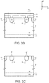
- Figure 4 is a top view, in the plane XY, of a portion of the device of Figure 3B , in particular of the region delimited by a dashed line and identified by the reference number 15 in Figure 3B .
- Figure 4 regards a manufacturing step intermediate between the steps of Figure 3B and Figure 3C , i.e., with the mask 13 still present but with the nickel layer 14 removed.
- irregular regions, or islands, 17 extend over the mask 13 and are due to an undesired reaction between the nickel and the silicon of the mask 13.
- indented regions extend underneath the mask 13, i.e., on the surface 2a of the drift layer 2.
- these indented regions are identified by the reference number 16 and are made of conductive material (including nickel).
- the extension in the plane XY, in particular along X, of said indented regions 16 were greater than the corresponding extension of the implanted regions 9', there would occur a short-circuit that would lead to breakdown of the device.
- an ohmic contact or quasi-ohmic contact would be formed on an area of an N type (which from the electrical standpoint is a resistance); there would therefore be a continuous passage of current both in forward biasing and in reverse biasing, with a consequent loss of the diode characteristics.
- FIG. 5 shows a MOSFET device 20 that comprises a semiconductor body 22, made of semiconductor material (which includes a substrate and, optionally, one or more epitaxial layers), having a top surface 22a and a bottom surface 22b.
- the semiconductor body 22 has, for example, an N- doping.
- body regions 25 (with a P doping) surround the source regions 28 (N+ doping).
- a respective insulating, or dielectric, layer 29 covers the gate structures 26.
- a top metal layer 30 is in electrical contact with the source regions 28 and the body regions 25, respectively, at respective surface portions 36 and 37 in order to bias, during use, the source regions 28 and the body regions 25 at a same biasing voltage.
- an interface region (with P+ doping) 34 is formed in the body regions 25, facing the top surface 22a at the surface portion 37.
- an interface ohmic contact layer 38 made of silicide is formed at the interface region 34 to form an ohmic contact between the metal 30 and the body region 25.
- a further interface ohmic contact layer 39 made of silicide is formed at the surface portion 36 to form an ohmic contact between the metal 30 and the source region 28.
- formation of the interface ohmic contact layers 38 and 39 envisages deposition of an intermediate metal layer, in particular a nickel, using the insulating layer 29, in a way similar to what has been described previously for the mask 13.
- This intermediate metal layer therefore extends over the insulating layer 29 and over the surface portions 36 and 37 in contact with the interface region 34 and the source region 28.
- a subsequent thermal annealing at high temperature (between 900°C and 1200°C for a time interval from 1 min to 120 min), enables formation of ohmic contacts made of nickel silicide, by chemical reaction between the deposited nickel and the silicon of the semiconductor body 22, at the surface portions 36 and 37 (more in particular, at the interface region 34 and the source region 28).
- a step of removal of the metal that extends over of the insulating layer 29 is carried out.
- the insulating layer 29, which has a function in the end device, is not removed.
- the applicant has noted a reaction between the nickel of the metal layer 14 and the insulating layer 29 where they are in direct contact (similarly to what is illustrated in Figure 4 ). Irregular regions, or islands, consequently extend over the insulating layer 29 and are due to an undesired reaction between the nickel and the silicon of the insulating layer 29. Since these islands are electrically conductive, they are a potential problem for operation of the device 20, above all in the case where their extension were such as to generate undesired short-circuits or other types of unexpected electrical connection. Insulation of the polysilicon 26 via covering of the oxide 29 is not uniform, and usually has a minimum at the highest point of the polysilicon step 26. If the reaction of the nickel with the silicon of the oxide occurs in this area, there is a high risk of creating a gate-to-source short-circuit owing to formation of a bridge between the metal 30 and the polysilicon 26.
- Patent document US 8,962,468 B1 relates to the field of wide band gap semiconductor wafer processing, and the formation of ohmic contacts and the devices made using the same. However, the above-mentioned issues are not solved.
- the aim of the present invention is to provide a SiC-based electronic device and a method for manufacturing the SiC-based electronic device, such as to overcome the drawbacks of the prior art.
- a SiC-based electronic device and a method for manufacturing the SiC-based electronic device are provided, as defined in the annexed claims.
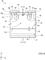
- Figure 6 shows, in side sectional view in a (triaxial) Cartesian reference system with axes X, Y, Z, a Merged-PiN-Schottky (MPS) device 50 according to one aspect of the present invention.
- MPS Merged-PiN-Schottky
- the MPS device 50 includes: a substrate 53, made of SiC of an N type, having a first dopant concentration, provided with a surface 53a opposite to a surface 53b, and having a thickness comprised between 50 ⁇ m and 350 ⁇ m, more in particular between 160 ⁇ m and 200 ⁇ m, for example equal to 180 ⁇ m; a drift layer (grown in an epitaxial way) 52, made of SiC of an N type, having a second dopant concentration lower than the first dopant concentration, which extends over the surface 53a of the substrate 53, and has a thickness comprised between 5 and 15 ⁇ m; an ohmic contact region, or layer, 56 (for example, made of nickel silicide), which extends over the surface 53b of the substrate 53; a cathode metallization 57, made, for example, of Ti/NiV/Ag or Ti/NiV/Au, which extends over the ohmic contact region 56; an anode metallization 58, made, for example
- One or more Schottky diodes 62 are formed at the interface between the drift layer 52 and the anode metallization 58, laterally to the implanted regions 59'.
- (semiconductor-metal) Schottky junctions are formed by portions of the drift layer 52 in direct electrical contact with respective portions of the anode metallization 58.
- the region of the MPS device 50 that includes the JB elements 59 and the Schottky diodes 62 is an active area 54 of the MPS device 50.
- each ohmic contact 59" is formed by one or more carbon-rich layers, including, for example, graphite layers, or graphene multi-layers. More in particular, each ohmic contact 59" has, on the surface 52a, a Si/C amorphous layer, where the carbon atoms are preponderant (for example, at least twice as high, in particular from 2 to 100 times as high) as compared to the silicon atoms, following upon phase separation between the silicon atoms and the carbon atoms of the SiC substrate.
- preponderant for example, at least twice as high, in particular from 2 to 100 times as high
- each ohmic contact 59" may present a layer including carbon clusters (e.g., a graphite layer), having a thickness greater than that of the amorphous layer.
- a layer including carbon clusters e.g., a graphite layer
- Such an ohmic contact 59" formation is due to thermal decomposition of the silicon carbide, as a result of the manufacturing process illustrated in what follows.
- the ohmic contacts 59" are self-aligned, on the surface 52a, with the implanted regions 59' (i.e., in top view in the plane XY, the ohmic contacts 59" have the same shape and extension as the implanted regions 59').
- the electrical contact between the anode metallization 58 and the implanted regions 59' occurs exclusively through the ohmic contacts 59". This feature translates into a technical advantage, in that it is possible to maximise the extension area of the ohmic contacts without the risk of short circuiting with neighbouring ohmic contacts.
- each ohmic contact 59" has the same shape and extension as the respective implanted region 59', there is no risk of an undesirable lateral extension of said ohmic contact beyond such implanted region 59'. Maximising the area of the ohmic contact allows maximising the current carried by said ohmic contact.
- the ohmic contacts 59" do not extend, along Z, beyond the surface 52a; in other words, the ohmic contacts 59" have a top surface 59a that is coplanar (i.e., aligned along X) with the surface 52a and extend in depth (along Z) within the ohmic contacts 59' by a depth comprised between one nanometre and some tens of nanometres (e.g., between 1 m and 20 m) measured starting from the surface 52a.
- Each ohmic contact 59" provides an electrical connection having an electrical resistivity value lower than the electrical resistivity value of the region that houses it.
- each ohmic contact 59" has an electrical resistance lower than the electrical resistance of the respective region 59' that houses it.
- a wafer 100 which includes a SiC substrate 53 (in particular, 4H-SiC; however, other polytypes may be used such as, but not exclusively, 2H-SiC, 3C-SiC and 6H-SiC).
- SiC substrate 53 in particular, 4H-SiC; however, other polytypes may be used such as, but not exclusively, 2H-SiC, 3C-SiC and 6H-SiC).
- the substrate 53 has a first conductivity type (in this embodiment, a doping of an N type) and is provided with a front surface 53a and a back surface 53b, which are opposite to one another along the axis Z.
- the substrate 53 has a dopant concentration comprised between 1.10 19 and 1.10 22 atoms/cm 3 .
- the front of the wafer 100 corresponds to the front surface 53a, and the back of the wafer 100 corresponds to the back surface 53b.
- the resistivity of the substrate 30 is, for example, comprised between 2 m ⁇ cm and 40 m ⁇ cm.
- the drift layer 52 Formed on the front surface 53a of the substrate 53, for example by epitaxial growth, is the drift layer 52, made of silicon carbide with the first conductivity type (N) and with a dopant concentration lower than that of the substrate 53, for example comprised between 1.10 14 and 5.10 16 atoms/cm 3 .
- the drift layer 52 is made of SiC, in particular 4H-SiC, but it is possible to use other SiC polytypes, such as 2H, 6H, 3C or 15R.
- the drift layer 52 has a thickness defined between a top side 52a and a bottom side 52b (the latter being in direct contact with the front surface 53a of the substrate 53) .
- a hard mask 70 is formed, for example by deposition of a photoresist, or TEOS or some other material designed for the purpose.
- the hard mask 70 has a thickness of between 0.5 ⁇ m and 2 ⁇ m or in any case a thickness such as to shield the implantation described hereinafter with reference to the same Figure 7B .
- the hard mask 70 extends in a region of the wafer 100 where, in subsequent steps, the active area 54 of the MPS device 50 will be formed.
- the hard mask 70 covers the regions of the top side 52a of the drift layer 52 that will form Schottky cells (diodes 62) and leaves exposed the regions of the top side 52a of the drift layer 52 that will form the implanted regions 59', already identified with reference to Figure 6 .
- a step of implantation of dopant species for example, boron or aluminium
- dopant species for example, boron or aluminium
- the second conductivity type here a P type
- the protection ring 60 if present, is also formed.
- the implantation step of Figure 4 comprises one or more implantations of dopant species, which have the second conductivity type, with an implantation energy comprised between 30 keV and 400 keV and with doses of between 1 ⁇ 10 12 atoms/cm 2 and 1 ⁇ 10 15 atoms/cm 2 , to form the implanted regions 59' with a dopant concentration of higher than 1 ⁇ 10 18 atoms/cm 3 .
- Implanted regions are thus formed having a depth, measured starting from the surface 52a, comprised between 0.4 ⁇ m and 1 ⁇ m.
- a laser source 80 is used configured to generate a beam 82 such as to heat the surface 52a (in particular, the implanted regions 59') locally up to a temperature of approximately 1500°C-2600°C.
- a temperature of approximately 2000°C at the level of the surface 52a is sufficient to guarantee temperatures within the range identified above also at the maximum depth reached by the implanted regions 59' (e.g., 1 ⁇ m).
- This temperature is such as to favour generation of ohmic contacts (for example, as has been said, including graphite and/or graphene) exclusively on the implanted regions 59', and not on the surface 52a that is not provided with the implanted regions 59'.
- This effect of a per se known type, is described for example by Maxime G. Lemaitre, "Low-temperature, site selective graphitization of SiC via ion implantation and pulsed laser annealing", APPLIED PHYSICS LETTERS 100, 193105 (2012 ).
- transformation of part of the implanted regions 59' into the ohmic contact 59" takes place by heating the entire wafer 100, appropriately moving the laser 80.
- transformation of the surface portions of the implanted regions 59' into the ohmic contact 59" is obtained by heating the useful surface of the wafer 100.
- useful surface is here meant the portion of surface of the drift layer 52 that includes the implanted regions 59', for example delimited externally by the edge-termination region 10.
- the useful surface might not correspond to the entire surface of the wafer 100 (for example, excluding possible portions of the wafer 100 that are lateral with respect to the active area 54, which are not of interest during use of the MPS device 50 in so far as they do not take part in transport of electric charge).
- a mask having regions transparent to the beam 82 (i.e., the beam 82 traverses them) and regions opaque to the beam 82 (i.e., the beam 82 does not traverse them, or traverses them in attenuated form such as not to heat significantly the portions of the wafer 100 that extend underneath).
- the transparent regions of the mask are aligned with the implanted regions 59', to enable the ohmic contact 59" formation.
- the implanted regions 59' (in particular, the dopants are activated, to obtain a concentration of dopant species comprised between approximately 1 ⁇ 10 17 atoms/cm 3 and 1 ⁇ 10 20 atoms/cm 3 ) are simultaneously formed and the ohmic contacts 59" for each implanted region.
- the ohmic contact is formed exclusively on the implanted regions 59', even in the absence of a mask there is a self-alignment between the implanted regions 59' and the respective ohmic contact 59".
- the localized and superficial increase in temperature causes the ohmic contact 59" formation; laterally to the implanted regions 59', no such effect is noted.
- the ohmic contact 59" formation takes place at temperatures comprised between 1200°C and 2600°C. According to the present invention, these temperatures are reached at a surface portion (some nanometres, e.g., 1-20 nm) of the implanted regions 59'. For greater depths, the temperature drops to values such as no longer to cause the ohmic contact 59" formation, which is thus self-limited. Therefore, the ohmic contact 59" does not extend throughout the thickness of the respective implanted region, but exclusively at a superficial level thereof.
- the laser 80 is, for example, a UV excimer laser. Other types of lasers may be used, among which lasers with wavelengths in the region of the visible.
- the parameters of configuration and actuation of the laser 80, optimized for achieving the purpose of the present invention, are the following:
- the area of the spot of the beam 82 at the level of the surface 52a is, for example, comprised between 0.7 and 1.5 cm 2 .
- one or more scans of the laser 80 are thus performed in the plane XY (e.g., a plurality of scans parallel to one another and to the axis X and/or axis Y) .
- Figure 8 illustrates, in this regard, experimental data of variation of the conduction current as a function of the voltage applied between anode and cathode of the MPS device 50.
- the curve S1 relates to electrical measurements at the PiN diode prior to the laser treatment
- the curve S2 relates to electrical measurements at the PiN diode after laser treatment, and therefore with the ohmic contact formed.
- the trends of the curves S1 and S2 confirm the expected behaviour.
- Figure 9 shows a MOSFET device 90 according to an aspect of the present invention.
- the MOSFET device 90 has an ohmic contact 91 at the interface region 34, between the metal 30 and the body region 25.
- the MOSFET device 90 moreover has a further ohmic contact 92 at the surface portion 36, between the metal 30 and the source region 28.
- both the ohmic contact 91 and the ohmic contact 92 are formed by one or more carbon-rich layers, which, for example, include graphite layers, or graphene multi-layers. More in particular, each ohmic contact 91, 92 has, on the surface 52a, a Si/C amorphous layer in which the carbon atoms are preponderant (for example, at least twice as high, in particular from 2 to 100 times as high) as compared to that of the silicon atoms, following upon phase separation between the silicon atoms and the carbon atoms of the SiC substrate.
- each ohmic contact 91, 92 can have a layer including carbon clusters (e.g., a graphite layer), having a thickness greater than that of the amorphous layer.
- a layer including carbon clusters e.g., a graphite layer
- Such an ohmic contact 59" formation is due to thermal decomposition of silicon carbide, as a result of the manufacturing process illustrated in what follows.
- the ohmic contact 91 and the ohmic contact 92 are self-aligned, on the surface 22a, with the interface region 34 and with the source region 28 (i.e., in top view in the plane XY, the ohmic contacts 91, 92 have the same shape and extension as the interface region 34 and the source region 28, respectively).
- the ohmic contacts 91 and 92 extend in depth (along Z) within the semiconductor body 22 by a depth comprised between one nanometre and some tens of nanometres (e.g., between 1 and 20 nm), measured starting from the surface 22a.
- Each ohmic contact 91, 92 provides an electrical connection having an electrical resistivity value lower than the electrical resistivity value of the region that houses it.
- each ohmic contact 91, 92 has an electrical resistance lower than the electrical resistance of the respective region 34, 28 that houses it.
- Figure 10 shows a wafer 200, which includes the MOSFET device 90 in an intermediate manufacturing stage, in which the body region 25, the interface region 34, the source region 28, the gate structures 26 and the insulating layer 29 have been formed (in a per se known manner).
- a thermal budget is generated on the surface 22a designed to favour generation, at the interface 34 and the source 28 regions, of the respective ohmic contact 91, 92.
- a laser source 95 is used configured to generate a beam 96 such as to heat the surface 22a locally (in particular, the interface 34 and the source 28 regions) up to a temperature of approximately 1200°C-2600°C.
- a temperature in the aforementioned range is such as to favour generation of the carbon-rich regions and graphite/graphene layers exclusively at the interface 34 and the source 28 regions, and not at the surface region 22a, where the interface 34 and the source 28 regions do not extend.
- transformation of the interface region 34 and source region 28 into the respective ohmic contact is obtained by heating the entire wafer 200, moving the laser 95 appropriately.
- transformation of the interface 34 and source 28 regions into the respective ohmic contact takes place by selectively heating the interface 34 and source 28 regions, by appropriately directing the beam 96.
- a mask (not illustrated in the figures) having regions transparent to the beam 96 (i.e., the beam 96 traverses them) and regions opaque to the beam 96 (i.e., the beam 96 does not traverse them, or traverses them in attenuated form such as not to significantly heat the masked portions of the wafer 200).
- the transparent regions of the mask are aligned with the interface 34 and source 28 regions in order to enable the formation of the respective ohmic contact and protect portions of the wafer 200 in which an ohmic contact formation via the laser 95 is not envisaged.
- the ohmic contact 92 formation at the source region 28 requires an energy of the beam 96 different from the energy required for the ohmic contact 91 formation at the interface region 34 (with P+ doping).
- optimization of the ohmic properties of the contact 92 at the source region 28 could require an energy of the beam 96 different from the energy required for optimization of the ohmic properties of the contact 91 at the interface region 34 (with P+ doping).
- the applicant has found that the ohmic contact 92 formation at the source region 28 (with N+ doping) and of the ohmic contact 91 at the interface region 34 (with P+ doping) can occur given the same energy of the beam.
- the parameters of configuration and actuation of the laser 95 are the following:
- the area of the spot of the beam 82 at the level of the surface 22a is, for example, comprised between 0.7 and 1.5 cm 2 .
- one or more scans of the laser 95 are therefore performed in the plane XY (e.g., a plurality of scans parallel to one another and to the axis X and/or axis Y).
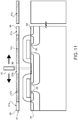
- Figure 11 it is possible to arrange a mask 97 on the wafer 200, said mask being provided with respective windows 97a, 97b at (i.e., vertically aligned with) the interface region 34 and the source region 28.
- the remaining portions 97c of the mask 97 are completely opaque to the beam 96, i.e., they are not traversed by the beam 96 (or in any case they are traversed in a non-significant way and such as not to generate on the underlying structures of the wafer 200 a heating such as to cause damage or undesired phenomena of some other type).
- the window 97a at the interface region 34 is provided with a filter 98 designed to modify characteristics of the beam 96, for example in the case where it were expedient to modify some characteristics of the beam that impinges on the interface region 34. Instead, the filter 98 is not present.
- the window 97b at the source region 28 does not have any filter; i.e., it is transparent to the beam 96, which traverses it in a substantially unaltered form as regards its characteristics.
- both of the windows 97a and 97b are without a filter, and that the mask 97 will have the function of protecting (via the opaque portions 97c) regions that are not to be heated with the beam 96.
- the beam 96 is generated by controlling the laser 95 in the following way:
- the area of the spot of the beam 82 at the level of the surface 22a is, for example, comprised between 0.7 and 1.5 cm 2 .
- one or more scans of the laser 95 are therefore performed in the plane XY (e.g., a plurality of scans parallel to one another and to the axis X and/or axis Y) .
- the beam 96 thus generated is directed towards the source region 28 (N+), through the window 97b, and towards the interface region 34 (P+), through the window 97a.
- the ohmic contact is formed exclusively at the P and N implanted regions, there is a self-alignment between the interface 34/source 28 regions and the respective ohmic contact 91/92.
- Transformation of the SiC into carbon-rich layers and/or graphite and/or graphene layers occurs on the basis of the technical considerations already described previously, with reference to manufacturing of the MPS device.
- the laser 95 is, for example, a UV excimer laser.
- Other types of laser may be used, among which lasers having wavelengths in the region of the visible.
- the conductivity types mentioned above may be switched to form a corresponding electronic device with opposite conductivity types as those described.
- the present invention applies to a P-channel device, in particular for forming ohmic contacts in, and activating dopant species of, regions having an N-type conductivity implanted in a substrate or semiconductor body having a P-type conductivity.
- the substrate 53 is of P type and the implanted region 59' is of N type.
- the present invention is not limited to an ohmic contact formation of an MPS device or of a MOSFET, but extends to an ohmic contact formation in a generic vertical-conduction electronic device, such as a Schottky diode, a JBS diode, a MOSFET, an IGBT, a JFET, a DMOS, etc.
Landscapes
- Electrodes Of Semiconductors (AREA)
- Bipolar Transistors (AREA)
- Ceramic Products (AREA)
Abstract
Description
- The present invention relates to a SiC-based electronic device and a method for manufacturing the SiC-based electronic device. In particular, the present invention relates to the formation of electrical contact regions of an ohmic type in the SiC-based electronic device.
- As is known, the semiconductor materials, which have a wide band gap, in particular, an energy value Eg of the band gap higher than 1.1 eV, a low ON-state resistance (RON), a high thermal conductivity value, a high operating frequency and a high rate of saturation of the charge carriers, are ideal for producing electronic components, such as diodes or transistors, in particular for power applications. A material having the above characteristics, and designed to be used for the manufacture of electronic components, is silicon carbide (SiC). In particular, the silicon carbide, in its different polytypes (for example, 3C-SiC, 4H-SiC, 6H-SiC), is preferable to silicon, as regards the properties listed previously.
- Electronic devices provided on a silicon-carbide substrate, as compared to similar devices provided on a silicon substrate, have numerous advantages, such as low output resistance in conduction, low leakage current, high operating temperature and high operating frequencies. In particular, SiC Schottky diodes have shown a higher switching performance, which render SiC electronic devices particularly favourable for high-frequency applications. Current applications impose requisites on the electrical properties and also on long-term reliability of the devices.
-
Figure 1 shows, in side sectional view in a (triaxial) Cartesian reference system of axes X, Y, Z, a merged-PiN-Schottky (MPS)device 1 of a known type. - The
MPS device 1 includes: asubstrate 3, made of SiC of an N type, having a first dopant concentration, provided with asurface 3a opposite to asurface 3b, and having a thickness of approximately 350 µm; a drift layer (grown in an epitaxial way) 2, made of SiC of an N type, having a second dopant concentration lower than the first dopant concentration, which extends over thesurface 3a of thesubstrate 3, and has a thickness comprised between 5 and 15 µm; an ohmic contact region 6 (for example, made of nickel silicide), which extends over thesurface 3b of thesubstrate 3; acathode metallization 16, which extends over theohmic contact region 6; ananode metallization 8, which extends over a top surface 2a of thedrift layer 2; multiple junction-barrier (JB)elements 9 in thedrift layer 2, which face the top surface 2a of thedrift layer 2 and each include a respective implanted region 9' of a P type and anohmic contact 9" made of metal material; and an edge-termination region, or protection ring, 10 (optional), in particular an implanted region of a P type, which surrounds theJB elements 9 completely. - Schottky
diodes 12 are formed at the interface between thedrift layer 2 and theanode metallization 8. In particular, Schottky junctions (semiconductor-metal) are formed by portions of thedrift layer 2 in direct electrical contact with respective portions of theanode metallization 8. - The region of the
MPS device 1 that includes theJB elements 9 and the Schottky diodes 12 (i.e., the region contained within the protection ring 10) is anactive area 4 of theMPS device 1. - With reference to
Figures 2A and 2B , the steps for manufacturing theMPS device 1 ofFigure 1 envisage (Figure 2A ) a step of masked implantation of dopant species (for example, boron or aluminium), which have the second conductivity type (P). The implantation is illustrated byarrows 18 inFigure 2A . For the implantation, amask 11 is used, in particular a hard mask made of silicon oxide or TEOS. Implanted regions 9' and the edge-termination region 10 are thus formed. Then,Figure 2B , themask 11 is removed, and a step of thermal annealing is carried out for diffusion and activation of the dopant species implanted in the step ofFigure 2A . The thermal annealing is, for example, carried out at a temperature higher than 1600°C (for example, between 1700°C and 1900°C and in some cases even higher). - With reference to
Figures 3A-3C , further steps ofohmic contact 9" formation are then carried out. With reference toFigure 3A , adeposition mask 13 made of silicon oxide or TEOS is formed, to cover surface regions of thedrift layer 2 other than the implanted regions 9' (and the edge-termination region 10, if present). In other words, themask 13 has throughopenings 13a at the implanted regions 9' (and optionally at least at one portion of the edge-termination region 10). Then,Figure 3B , a deposition of nickel is performed on themask 13 and within the throughopenings 13a (themetal layer 14 inFigure 3B ). The nickel thus deposited reaches and contacts the implanted regions 9' and the edge-termination region 10 through the throughopenings 13a. - With reference to
Figure 3C , a subsequent thermal annealing at high temperature (between 900°C and 1200°C) for a time interval from 1 min to 120 min, enables formation of nickel-silicide ohmic contacts 9", by chemical reaction between the nickel deposited and the silicon of thedrift layer 2 at thethrough openings 13a. In fact, the deposited nickel reacts where it comes into contact with the surface material of thedrift layer 2, forming Ni2Si (i.e., the ohmic contact). Next, a step of removal of the metal that extends over of themask 13 and removal of themask 13 is carried out. - The present applicant has found that an albeit limited reaction occurs in any case between the nickel of the
metal layer 14 and themask 13, where they are in direct contact, as illustrated by way of example inFigure 4. Figure 4 is a top view, in the plane XY, of a portion of the device ofFigure 3B , in particular of the region delimited by a dashed line and identified by thereference number 15 inFigure 3B .Figure 4 regards a manufacturing step intermediate between the steps ofFigure 3B and Figure 3C , i.e., with themask 13 still present but with thenickel layer 14 removed. As may be noted fromFigure 4 , irregular regions, or islands, 17 extend over themask 13 and are due to an undesired reaction between the nickel and the silicon of themask 13. The applicant has moreover noted that similar indented regions extend underneath themask 13, i.e., on the surface 2a of thedrift layer 2. InFigure 4 , these indented regions are identified by thereference number 16 and are made of conductive material (including nickel). In the case where the extension in the plane XY, in particular along X, of saidindented regions 16 were greater than the corresponding extension of the implanted regions 9', there would occur a short-circuit that would lead to breakdown of the device. In detail, in the case where the undesired conductive regions were to extend in the area dedicated to the Schottky contact, an ohmic contact or quasi-ohmic contact (Schottky contact with low barrier) would be formed on an area of an N type (which from the electrical standpoint is a resistance); there would therefore be a continuous passage of current both in forward biasing and in reverse biasing, with a consequent loss of the diode characteristics. - The same problem is encountered during ohmic contact formation at body and source regions of a SiC MOSFET device.
-
Figure 5 shows aMOSFET device 20 that comprises asemiconductor body 22, made of semiconductor material (which includes a substrate and, optionally, one or more epitaxial layers), having atop surface 22a and abottom surface 22b. Thesemiconductor body 22 has, for example, an N- doping. Adrain region 24, for example formed by implanting dopant species of an N type (N+ doping), extends at thebottom surface 22b. At thetop surface 22a body regions 25 (with a P doping) surround the source regions 28 (N+ doping). Thegate structures 26, including a stack formed by a gateconductive layer 26a (e.g., polysilicon) and by a gatedielectric layer 26b, extend over thetop surface 22a, in part overlapping thesource regions 28. A respective insulating, or dielectric, layer 29 (for example, made of silicon oxide or TEOS) covers thegate structures 26. - A
top metal layer 30 is in electrical contact with thesource regions 28 and thebody regions 25, respectively, atrespective surface portions source regions 28 and thebody regions 25 at a same biasing voltage. - To improve the electrical contact between the
top metal layer 30 and thebody regions 25, an interface region (with P+ doping) 34 is formed in thebody regions 25, facing thetop surface 22a at thesurface portion 37. Typically, an interfaceohmic contact layer 38 made of silicide is formed at theinterface region 34 to form an ohmic contact between themetal 30 and thebody region 25. Likewise, a further interfaceohmic contact layer 39 made of silicide is formed at thesurface portion 36 to form an ohmic contact between themetal 30 and thesource region 28. - As described with reference to
Figures 3A-3C , formation of the interfaceohmic contact layers insulating layer 29, in a way similar to what has been described previously for themask 13. This intermediate metal layer therefore extends over theinsulating layer 29 and over thesurface portions interface region 34 and thesource region 28. - As described with reference to
Figure 3C , a subsequent thermal annealing at high temperature (between 900°C and 1200°C for a time interval from 1 min to 120 min), enables formation of ohmic contacts made of nickel silicide, by chemical reaction between the deposited nickel and the silicon of thesemiconductor body 22, at thesurface portions 36 and 37 (more in particular, at theinterface region 34 and the source region 28). Next, a step of removal of the metal that extends over of theinsulating layer 29 is carried out. Theinsulating layer 29, which has a function in the end device, is not removed. - However, as described previously, the applicant has noted a reaction between the nickel of the
metal layer 14 and theinsulating layer 29 where they are in direct contact (similarly to what is illustrated inFigure 4 ). Irregular regions, or islands, consequently extend over theinsulating layer 29 and are due to an undesired reaction between the nickel and the silicon of theinsulating layer 29. Since these islands are electrically conductive, they are a potential problem for operation of thedevice 20, above all in the case where their extension were such as to generate undesired short-circuits or other types of unexpected electrical connection. Insulation of thepolysilicon 26 via covering of theoxide 29 is not uniform, and usually has a minimum at the highest point of thepolysilicon step 26. If the reaction of the nickel with the silicon of the oxide occurs in this area, there is a high risk of creating a gate-to-source short-circuit owing to formation of a bridge between themetal 30 and thepolysilicon 26. - Patent document
US 8,962,468 B1 relates to the field of wide band gap semiconductor wafer processing, and the formation of ohmic contacts and the devices made using the same. However, the above-mentioned issues are not solved. - The aim of the present invention is to provide a SiC-based electronic device and a method for manufacturing the SiC-based electronic device, such as to overcome the drawbacks of the prior art.
- According to the present invention, a SiC-based electronic device and a method for manufacturing the SiC-based electronic device are provided, as defined in the annexed claims.
- For a better understanding of the present invention, preferred embodiments thereof are now described, purely by way of non-limiting example, with reference to the attached drawings, wherein:
-
Figure 1 shows, in cross-sectional view, an MPS device according to a known embodiment; -
Figures 2A and 2B show, in cross-sectional view, intermediate steps for manufacturing the MPS device ofFigure 1 , according to the known art; and -
Figures 3A-3C show, in cross-sectional view, steps for ohmic contact formation in the MPS device ofFigure 1 , subsequent to the steps ofFigures 2A and 2B , according to the known art; -
Figure 4 illustrates, in top view, undesired regions that have formed as a result of the manufacturing steps ofFigures 3A-3B , according to the known art; -
Figure 5 shows, in cross-sectional view, a MOSFET device according to a known embodiment; -
Figure 6 shows, in cross-sectional view, an MPS device according to one embodiment of the present invention; -
Figures 7A-7D illustrate, in cross-sectional view, steps for manufacturing the MPS device ofFigure 6 , according to the present invention; -
Figure 8 illustrates voltage-current curves of the MPS device ofFigure 6 ; -
Figure 9 illustrates, in cross-sectional view, a MOSFET device according to one embodiment of the present invention; -
Figure 10 illustrates, in cross-sectional view, a step for manufacturing the MOSFET device ofFigure 9 , according to one embodiment of the present invention; and -
Figure 11 illustrates, in cross-sectional view, a step for manufacturing the MOSFET device ofFigure 9 , according to a further embodiment of the present invention. - The present invention will be described with reference to two possible embodiments, specifically with reference to a merged-PiN-Schottky (MPS) device (
Figures 6 ,7A-7D ) and with reference to a MOSFET device (Figures 9-11 ); however, as will be evident from the ensuing description, the present invention applies in general to any SiC-based electronic device. -
Figure 6 shows, in side sectional view in a (triaxial) Cartesian reference system with axes X, Y, Z, a Merged-PiN-Schottky (MPS)device 50 according to one aspect of the present invention. - The MPS device 50 includes: a substrate 53, made of SiC of an N type, having a first dopant concentration, provided with a surface 53a opposite to a surface 53b, and having a thickness comprised between 50 µm and 350 µm, more in particular between 160 µm and 200 µm, for example equal to 180 µm; a drift layer (grown in an epitaxial way) 52, made of SiC of an N type, having a second dopant concentration lower than the first dopant concentration, which extends over the surface 53a of the substrate 53, and has a thickness comprised between 5 and 15 µm; an ohmic contact region, or layer, 56 (for example, made of nickel silicide), which extends over the surface 53b of the substrate 53; a cathode metallization 57, made, for example, of Ti/NiV/Ag or Ti/NiV/Au, which extends over the ohmic contact region 56; an anode metallization 58, made, for example, of Ti/AlSiCu or Ni/AlSiCu, which extends over a top surface 52a of the drift layer 52; a passivation layer 69 on the anode metallization 58, for protecting the latter; multiple junction-barrier (JB) elements 59 in the drift layer 52, which face the top surface 52a of the drift layer 52 and each include a respective implanted region 59' of a P type and an ohmic contact 59"; and an edge-termination region, or protection ring, 60 (optional), in particular an implanted region of a P type, which completely surrounds the junction-barrier elements 59.
- One or
more Schottky diodes 62 are formed at the interface between thedrift layer 52 and theanode metallization 58, laterally to the implanted regions 59'. In particular, (semiconductor-metal) Schottky junctions are formed by portions of thedrift layer 52 in direct electrical contact with respective portions of theanode metallization 58. - The region of the
MPS device 50 that includes theJB elements 59 and the Schottky diodes 62 (i.e., the region contained within the protection ring 60) is anactive area 54 of theMPS device 50. - According to one aspect of the present invention, each
ohmic contact 59" is formed by one or more carbon-rich layers, including, for example, graphite layers, or graphene multi-layers. More in particular, eachohmic contact 59" has, on thesurface 52a, a Si/C amorphous layer, where the carbon atoms are preponderant (for example, at least twice as high, in particular from 2 to 100 times as high) as compared to the silicon atoms, following upon phase separation between the silicon atoms and the carbon atoms of the SiC substrate. Underneath this amorphous layer, eachohmic contact 59" may present a layer including carbon clusters (e.g., a graphite layer), having a thickness greater than that of the amorphous layer. Such anohmic contact 59" formation is due to thermal decomposition of the silicon carbide, as a result of the manufacturing process illustrated in what follows. - According to a further aspect of the present invention, the
ohmic contacts 59" are self-aligned, on thesurface 52a, with the implanted regions 59' (i.e., in top view in the plane XY, theohmic contacts 59" have the same shape and extension as the implanted regions 59'). In this case, the electrical contact between theanode metallization 58 and the implanted regions 59' occurs exclusively through theohmic contacts 59". This feature translates into a technical advantage, in that it is possible to maximise the extension area of the ohmic contacts without the risk of short circuiting with neighbouring ohmic contacts. In fact, since eachohmic contact 59" has the same shape and extension as the respective implanted region 59', there is no risk of an undesirable lateral extension of said ohmic contact beyond such implanted region 59'. Maximising the area of the ohmic contact allows maximising the current carried by said ohmic contact. - Moreover, according to a further aspect of the present invention, the
ohmic contacts 59" do not extend, along Z, beyond thesurface 52a; in other words, theohmic contacts 59" have atop surface 59a that is coplanar (i.e., aligned along X) with thesurface 52a and extend in depth (along Z) within the ohmic contacts 59' by a depth comprised between one nanometre and some tens of nanometres (e.g., between 1 m and 20 m) measured starting from thesurface 52a. - Each
ohmic contact 59" provides an electrical connection having an electrical resistivity value lower than the electrical resistivity value of the region that houses it. In particular, eachohmic contact 59" has an electrical resistance lower than the electrical resistance of the respective region 59' that houses it. - The steps of the ohmic contact 59' formation are described in what follows, with explicit reference to the steps for manufacturing the MPS device 50 (
Figures 7A-7D ). - With reference to
Figure 7A , awafer 100 is provided, which includes a SiC substrate 53 (in particular, 4H-SiC; however, other polytypes may be used such as, but not exclusively, 2H-SiC, 3C-SiC and 6H-SiC). - The
substrate 53 has a first conductivity type (in this embodiment, a doping of an N type) and is provided with afront surface 53a and aback surface 53b, which are opposite to one another along the axis Z. Thesubstrate 53 has a dopant concentration comprised between 1.1019 and 1.1022 atoms/cm3. - The front of the
wafer 100 corresponds to thefront surface 53a, and the back of thewafer 100 corresponds to theback surface 53b. The resistivity of thesubstrate 30 is, for example, comprised between 2 mΩ·cm and 40 mΩ·cm. - Formed on the
front surface 53a of thesubstrate 53, for example by epitaxial growth, is thedrift layer 52, made of silicon carbide with the first conductivity type (N) and with a dopant concentration lower than that of thesubstrate 53, for example comprised between 1.1014 and 5.1016 atoms/cm3. Thedrift layer 52 is made of SiC, in particular 4H-SiC, but it is possible to use other SiC polytypes, such as 2H, 6H, 3C or 15R. - The
drift layer 52 has a thickness defined between atop side 52a and abottom side 52b (the latter being in direct contact with thefront surface 53a of the substrate 53) . - Then,
Figure 7B , on thetop side 52a of thedrift layer 52 ahard mask 70 is formed, for example by deposition of a photoresist, or TEOS or some other material designed for the purpose. Thehard mask 70 has a thickness of between 0.5 µm and 2 µm or in any case a thickness such as to shield the implantation described hereinafter with reference to the sameFigure 7B . Thehard mask 70 extends in a region of thewafer 100 where, in subsequent steps, theactive area 54 of theMPS device 50 will be formed. - In top view, in the plane XY, the
hard mask 70 covers the regions of thetop side 52a of thedrift layer 52 that will form Schottky cells (diodes 62) and leaves exposed the regions of thetop side 52a of thedrift layer 52 that will form the implanted regions 59', already identified with reference toFigure 6 . - Then a step of implantation of dopant species (for example, boron or aluminium) is carried out, which have the second conductivity type (here a P type), exploiting the hard mask 70 (the implantation is indicated in the figure by the arrows 72). During the step of
Figure 7B , theprotection ring 60, if present, is also formed. - In an embodiment provided by way of example, the implantation step of
Figure 4 comprises one or more implantations of dopant species, which have the second conductivity type, with an implantation energy comprised between 30 keV and 400 keV and with doses of between 1·1012 atoms/cm2 and 1·1015 atoms/cm2, to form the implanted regions 59' with a dopant concentration of higher than 1·1018 atoms/cm3. Implanted regions are thus formed having a depth, measured starting from thesurface 52a, comprised between 0.4 µm and 1 µm. - Next,
Figure 7C , themask 70 is removed and,Figure 7D , on thesurface 52a a thermal budget is generated designed to favour generation, on the implanted regions 59'. - For this purpose, a
laser source 80 is used configured to generate abeam 82 such as to heat thesurface 52a (in particular, the implanted regions 59') locally up to a temperature of approximately 1500°C-2600°C. Given the maximum depth of the implanted regions 59', a temperature of approximately 2000°C at the level of thesurface 52a is sufficient to guarantee temperatures within the range identified above also at the maximum depth reached by the implanted regions 59' (e.g., 1 µm). - This temperature is such as to favour generation of ohmic contacts (for example, as has been said, including graphite and/or graphene) exclusively on the implanted regions 59', and not on the
surface 52a that is not provided with the implanted regions 59'. This effect, of a per se known type, is described for example by Maxime G. Lemaitre, "Low-temperature, site selective graphitization of SiC via ion implantation and pulsed laser annealing", ). - In one embodiment, transformation of part of the implanted regions 59' into the
ohmic contact 59" takes place by heating theentire wafer 100, appropriately moving thelaser 80. - In a further embodiment, transformation of the surface portions of the implanted regions 59' into the
ohmic contact 59" is obtained by heating the useful surface of thewafer 100. By "useful surface" is here meant the portion of surface of thedrift layer 52 that includes the implanted regions 59', for example delimited externally by the edge-termination region 10. The useful surface might not correspond to the entire surface of the wafer 100 (for example, excluding possible portions of thewafer 100 that are lateral with respect to theactive area 54, which are not of interest during use of theMPS device 50 in so far as they do not take part in transport of electric charge). - In a further embodiment, it is possible to arrange over the
surface 52a (in contact with thesurface 52a or at a distance therefrom) a mask having regions transparent to the beam 82 (i.e., thebeam 82 traverses them) and regions opaque to the beam 82 (i.e., thebeam 82 does not traverse them, or traverses them in attenuated form such as not to heat significantly the portions of thewafer 100 that extend underneath). The transparent regions of the mask are aligned with the implanted regions 59', to enable theohmic contact 59" formation. - Optionally, and independent of the embodiment used, the implanted regions 59' (in particular, the dopants are activated, to obtain a concentration of dopant species comprised between approximately 1·1017 atoms/cm3 and 1·1020 atoms/cm3) are simultaneously formed and the
ohmic contacts 59" for each implanted region. - Furthermore, since the ohmic contact is formed exclusively on the implanted regions 59', even in the absence of a mask there is a self-alignment between the implanted regions 59' and the respective
ohmic contact 59". - At the implanted regions 59', the localized and superficial increase in temperature causes the
ohmic contact 59" formation; laterally to the implanted regions 59', no such effect is noted. Theohmic contact 59" formation takes place at temperatures comprised between 1200°C and 2600°C. According to the present invention, these temperatures are reached at a surface portion (some nanometres, e.g., 1-20 nm) of the implanted regions 59'. For greater depths, the temperature drops to values such as no longer to cause theohmic contact 59" formation, which is thus self-limited. Therefore, theohmic contact 59" does not extend throughout the thickness of the respective implanted region, but exclusively at a superficial level thereof. - The
laser 80 is, for example, a UV excimer laser. Other types of lasers may be used, among which lasers with wavelengths in the region of the visible. - The parameters of configuration and actuation of the
laser 80, optimized for achieving the purpose of the present invention, are the following: - wavelength: between 290 nm and 370 nm, in particular 310 nm;
- pulse duration: between 100 ns and 300 ns, in particular 160 ns;
- number of pulses: between 1 and 10, in particular 2;
- energy density: between (2) 1.6 and 4 J/cm2, in particular (3) 2.6 J/cm2 (considered at the level of the
surface 52a); and - temperature: between 1400°C and 2600°C, in particular 1800°C (considered at the level of the
surface 52a). - The area of the spot of the
beam 82 at the level of thesurface 52a is, for example, comprised between 0.7 and 1.5 cm2. - To cover the
entire wafer 100, or the sub-region of thewafer 100 to be heated, one or more scans of thelaser 80 are thus performed in the plane XY (e.g., a plurality of scans parallel to one another and to the axis X and/or axis Y) . - The applicant has, however, found that, with the parameters identified previously, the desired electrical behaviour is obtained for the
MPS device 50.Figure 8 illustrates, in this regard, experimental data of variation of the conduction current as a function of the voltage applied between anode and cathode of theMPS device 50. The curve S1 relates to electrical measurements at the PiN diode prior to the laser treatment, whereas the curve S2 relates to electrical measurements at the PiN diode after laser treatment, and therefore with the ohmic contact formed. The trends of the curves S1 and S2 confirm the expected behaviour. -
Figure 9 shows aMOSFET device 90 according to an aspect of the present invention. - Technical elements and characteristics of the
MOSFET device 90 that are common to theMOSFET device 20 ofFigure 5 are illustrated with the same reference numbers and are not described any further. - Unlike the
MOSFET device 20, theMOSFET device 90 has anohmic contact 91 at theinterface region 34, between themetal 30 and thebody region 25. TheMOSFET device 90 moreover has a furtherohmic contact 92 at thesurface portion 36, between themetal 30 and thesource region 28. - According to one aspect of the present invention, both the
ohmic contact 91 and theohmic contact 92 are formed by one or more carbon-rich layers, which, for example, include graphite layers, or graphene multi-layers. More in particular, eachohmic contact surface 52a, a Si/C amorphous layer in which the carbon atoms are preponderant (for example, at least twice as high, in particular from 2 to 100 times as high) as compared to that of the silicon atoms, following upon phase separation between the silicon atoms and the carbon atoms of the SiC substrate. Underneath this amorphous layer, eachohmic contact ohmic contact 59" formation is due to thermal decomposition of silicon carbide, as a result of the manufacturing process illustrated in what follows. - According to a further aspect of the present invention, the
ohmic contact 91 and theohmic contact 92 are self-aligned, on thesurface 22a, with theinterface region 34 and with the source region 28 (i.e., in top view in the plane XY, theohmic contacts interface region 34 and thesource region 28, respectively). - The
ohmic contacts semiconductor body 22 by a depth comprised between one nanometre and some tens of nanometres (e.g., between 1 and 20 nm), measured starting from thesurface 22a. - Each
ohmic contact ohmic contact respective region - The steps of formation of the
ohmic contacts Figure 10 . - In particular,
Figure 10 shows awafer 200, which includes theMOSFET device 90 in an intermediate manufacturing stage, in which thebody region 25, theinterface region 34, thesource region 28, thegate structures 26 and the insulatinglayer 29 have been formed (in a per se known manner). - In order to form the
ohmic contacts surface 22a designed to favour generation, at theinterface 34 and thesource 28 regions, of the respectiveohmic contact - For this purpose, a
laser source 95 is used configured to generate abeam 96 such as to heat thesurface 22a locally (in particular, theinterface 34 and thesource 28 regions) up to a temperature of approximately 1200°C-2600°C. - A temperature in the aforementioned range is such as to favour generation of the carbon-rich regions and graphite/graphene layers exclusively at the
interface 34 and thesource 28 regions, and not at thesurface region 22a, where theinterface 34 and thesource 28 regions do not extend. - In one embodiment, transformation of the
interface region 34 andsource region 28 into the respective ohmic contact is obtained by heating theentire wafer 200, moving thelaser 95 appropriately. - In a further embodiment, transformation of the
interface 34 andsource 28 regions into the respective ohmic contact takes place by selectively heating theinterface 34 andsource 28 regions, by appropriately directing thebeam 96. - In a further embodiment, it is possible to arrange on the wafer 200 a mask (not illustrated in the figures) having regions transparent to the beam 96 (i.e., the
beam 96 traverses them) and regions opaque to the beam 96 (i.e., thebeam 96 does not traverse them, or traverses them in attenuated form such as not to significantly heat the masked portions of the wafer 200). The transparent regions of the mask are aligned with theinterface 34 andsource 28 regions in order to enable the formation of the respective ohmic contact and protect portions of thewafer 200 in which an ohmic contact formation via thelaser 95 is not envisaged. - The applicant has found that the
ohmic contact 92 formation at the source region 28 (with N+ doping) requires an energy of thebeam 96 different from the energy required for theohmic contact 91 formation at the interface region 34 (with P+ doping). - Optimization of the ohmic properties of the
contact 92 at the source region 28 (with N+ doping) could require an energy of thebeam 96 different from the energy required for optimization of the ohmic properties of thecontact 91 at the interface region 34 (with P+ doping). For this purpose, it is possible to regulate operating parameters of thelaser 95 for generating arespective beam 96 at theinterface region 34 and at thesource region 28, each beam being designed for generating the respective layer with ohmic properties. - In any case, the applicant has found that the
ohmic contact 92 formation at the source region 28 (with N+ doping) and of theohmic contact 91 at the interface region 34 (with P+ doping) can occur given the same energy of the beam. - In detail, at the
source 28 andinterface 34 regions, the parameters of configuration and actuation of thelaser 95, optimized for achieving the purpose of the present invention, are the following: - wavelength: between 290 nm and 370 nm, in particular 310 nm;
- pulse duration: between 100 ns and 300 ns, in particular 160 ns;
- number of pulses: between 1 and 10, in particular 2;
- energy density: between (2) 1.6 and 4 J/cm2, in particular (3) 2.6 J/cm2 (considered at the level of the
surface 22a); - temperature: between 1400°C and 2600°C, in particular 1800°C (considered at the level of the
surface 22a). - The area of the spot of the
beam 82 at the level of thesurface 22a is, for example, comprised between 0.7 and 1.5 cm2. - To cover the
entire wafer 200 or the sub-region of thewafer 200 to be heated, one or more scans of thelaser 95 are therefore performed in the plane XY (e.g., a plurality of scans parallel to one another and to the axis X and/or axis Y). - Alternatively,
Figure 11 , it is possible to arrange amask 97 on thewafer 200, said mask being provided withrespective windows interface region 34 and thesource region 28. The remainingportions 97c of themask 97 are completely opaque to thebeam 96, i.e., they are not traversed by the beam 96 (or in any case they are traversed in a non-significant way and such as not to generate on the underlying structures of the wafer 200 a heating such as to cause damage or undesired phenomena of some other type). - The
window 97a at theinterface region 34 is provided with afilter 98 designed to modify characteristics of thebeam 96, for example in the case where it were expedient to modify some characteristics of the beam that impinges on theinterface region 34. Instead, thefilter 98 is not present. Thewindow 97b at thesource region 28 does not have any filter; i.e., it is transparent to thebeam 96, which traverses it in a substantially unaltered form as regards its characteristics. - In the following of the present invention, it is considered that both of the
windows mask 97 will have the function of protecting (via theopaque portions 97c) regions that are not to be heated with thebeam 96. - In particular, in this embodiment, the
beam 96 is generated by controlling thelaser 95 in the following way: - wavelength: between 290 nm and 370 nm, in particular 310 nm;
- pulse duration: between 100 ns and 300 ns, in particular 160 ns;
- number of pulses: between 1 and 10, in particular 2;
- energy density: between (2) 1.6 and 4 J/cm2, in particular (3) 2.6 J/cm2 (considered at the level of the
surface 22a); - temperature: between 1400°C and 2600°C, in particular 1800°C (considered at the level of the
surface 22a). - The area of the spot of the
beam 82 at the level of thesurface 22a is, for example, comprised between 0.7 and 1.5 cm2. - To cover the
entire wafer 200, or the sub-region of thewafer 200 to be heated, one or more scans of thelaser 95 are therefore performed in the plane XY (e.g., a plurality of scans parallel to one another and to the axis X and/or axis Y) . - The
beam 96 thus generated is directed towards the source region 28 (N+), through thewindow 97b, and towards the interface region 34 (P+), through thewindow 97a. - It is evident that, according to a further embodiment, it is possible to introduce a filter also at the
window 97b, and generate thebeam 96 in an appropriate way (i.e., such that the filtered beam is designed to generate the ohmic contact at the source region 28). - Since the ohmic contact is formed exclusively at the P and N implanted regions, there is a self-alignment between the
interface 34/source 28 regions and the respectiveohmic contact 91/92. - Transformation of the SiC into carbon-rich layers and/or graphite and/or graphene layers occurs on the basis of the technical considerations already described previously, with reference to manufacturing of the MPS device.
- The
laser 95 is, for example, a UV excimer laser. Other types of laser may be used, among which lasers having wavelengths in the region of the visible. - From an examination of the characteristics of the invention provided according to the present disclosure the advantages that it affords are evident.
- In particular, according to the present invention, it is possible, with a single process, to provide ohmic contacts on P+ or N+ regions, without any deposition of metal layers, thus overcoming the disadvantages regarding the known art identified and described previously.
- Finally, it is clear that modifications and variations may be made to what has been described and illustrated herein, without thereby departing from the scope of the present invention, as defined in the annexed claims.
- For example, the conductivity types mentioned above (N-type and P-type) may be switched to form a corresponding electronic device with opposite conductivity types as those described. In particular, the present invention applies to a P-channel device, in particular for forming ohmic contacts in, and activating dopant species of, regions having an N-type conductivity implanted in a substrate or semiconductor body having a P-type conductivity. In this case, the
substrate 53 is of P type and the implanted region 59' is of N type. - Moreover, as already noted previously, the present invention is not limited to an ohmic contact formation of an MPS device or of a MOSFET, but extends to an ohmic contact formation in a generic vertical-conduction electronic device, such as a Schottky diode, a JBS diode, a MOSFET, an IGBT, a JFET, a DMOS, etc.
Claims (28)
- A method for manufacturing an electronic device (50; 90), comprising the steps of:- forming, at a front side (52a; 22a) of a solid body (52; 22) of Silicon Carbide, SiC, having dopants of a first conductivity type, an implanted region (59'; 34) by implanting dopants of a second conductivity type, the first conductivity type being different than the second conductivity type, the implanted region (59'; 34) extending in the solid body (52; 22) from the front side toward a bottom side, the implanted region (59'; 34) having a top surface that is coplanar with at least a surface portion of said front side of the solid body; and- generating a first laser beam (82; 96) directed towards said implanted region (59'; 34) in order to heat the implanted region (59'; 34) to temperatures in the range 1500°C - 2600°C thereby forming a first carbon-rich electrical-contact region (59"; 91) at said implanted region (59'; 34).
- The method according to claim 1, wherein forming the first ohmic contact region (59"; 91) comprises forming one or more graphene and/or graphite layers within the implanted region (59'; 34).
- The method according to claim 1 or claim 2, wherein said ohmic contact region (59") has, in top plan view, form and extension coinciding with form and extension of the implanted region (59').
- The method according to any one of the preceding claims, wherein said first laser beam (82; 96) is generated with the following parameters:- wavelength: between 290 nm and 370 nm, in particular 310 nm;- pulse duration: between 100 ns and 300 ns, in particular 160 ns;- number of pulses: between 1 and 10, in particular 2; and- energy density: between 1.6 and 4 J/cm2, in particular 2.6 J/cm2.
- The method according to any one of the preceding claims, wherein said first electrical-contact region (59"; 34) forms a first ohmic contact having a top surface thereof coinciding with the top surface of the implanted region (59'; 34) .
- The method according to any one of the preceding claims, wherein said first electrical-contact region (59"; 91) has a thickness in the range 1 nm - 20 nm.
- The method according to any one of the preceding claims, wherein the material of the solid body is one among: 4H-SiC, 6H-SiC, 3C-SiC, 15R-SiC.
- The method according to any one of the preceding claims, wherein said electronic device (50; 90) is one among: a merged-PiN-Schottky diode, Schottky diodes, JBS diodes, MOSFETs, IGBTs, JFETs, and DMOSs.
- The method according to any one of the preceding claims, wherein said electronic device (50) is a merged-PiN-Schottky, MPS, diode, the method comprising the steps of:- forming said solid body, including:arranging a SiC substrate with the first conductivity type having a front side thereof and a back side thereof opposite to one another, andepitaxially growing, on the front side of the substrate, a drift layer (52) of SiC with the first conductivity type;- forming a first electrical terminal (58) in electrical contact with the doped region (59') via the first electrical-contact region (59") and in direct electrical contact with the drift layer (52) laterally to the doped region (59') so as to form a junction-barrier (JB) diode with said doped region (59') and a Schottky diode with the drift layer (52); and- forming a second electrical terminal (57) on the back side of the substrate.
- The method according to any one of the claims 1 to 8, wherein said electronic device (90) is a MOSFET, the method comprising the steps of:forming, on said front side (22a) of the solid body (22), a first body region (25) having the second conductivity type;forming said implanted region (34) within the first body region (25);forming, on said front side (22a) of the solid body (22), a second body region (25) having the second conductivity type, which extends laterally to the first body region (25);forming, in the second body region (25), a source region (28) having the first conductivity type;generating a second laser beam (96) directed towards said source region (28) in order to generate heating of the source region (28) to temperatures in the range 1500°C - 2600°C so as to form a second carbon-rich electrical-contact region (92) at said source region (28).
- The method according to claim 10, wherein said second laser beam (96) is generated with the following parameters:- wavelength: between 290 nm and 370 nm, in particular 310 nm;- pulse duration: between 100 ns and 300 ns, in particular 160 ns;- number of pulses: between 1 and 10, in particular 2; and- energy density: between 2 and 4 J/cm2, in particular 3J/cm2.
- The method according to claim 10 or 11, wherein forming the second ohmic contact region (92) comprises forming one or more graphene and/or graphite layers within the source region (28).
- The method according to any one of the preceding claims, wherein said first electrical-contact region (59"; 34) forms a first ohmic contact having a top surface thereof coinciding with the top surface of the implanted region (59'; 34) .
- The method according to any one of the claims 10 to 13, wherein said second electrical-contact region (59"; 91) has a thickness in the range 1 nm - 20 nm.
- The method according to any one of the preceding claims, wherein the first conductivity type is N-type and the second conductivity type is P-type, or vice versa.
- An electronic device (50; 90), comprising:- a solid body (52; 22) of Silicon Carbide, SiC, having a first conductivity type;- an implanted region (59'; 34), which extends at a front side (52a; 22a) of the solid body (52; 22) and includes dopant species of a second conductivity type, the first conductivity type being different than the second conductivity type, said implanted region having a top surface coplanar with at least a surface portion of said front side (52a; 22a) of the solid body; and- a first carbon-rich electrical-contact region (59"; 91), which extends at said implanted region (59'; 34).
- The device according to claim 16, wherein the first electrical-contact region (59"; 91) comprises one or more graphene and/or graphite layers within the implanted region (59'; 34).
- The device according to claim 17, wherein said first electrical-contact region (59"; 91) forms an ohmic contact having a top surface thereof coinciding with the top surface of the implanted region (59'; 34).
- The device according to any one of claims 16-18, wherein said ohmic contact region (59") has, in top plan view, form and extension coinciding with form and extension of the implanted region (59').
- The device according to any one of the claims 16-19, wherein said electrical-contact region (59") has a thickness in the range 1 nm - 20 nm.
- The device according to any one of the claims 16-20, wherein the material of the solid body is one among: 4H-SiC, 6H-SiC, 3C-SiC, 15R-SiC.
- The device according to any one of the claims 16-21, being one among: a merged-PiN-Schottky diode, Schottky diodes, JBS diodes, MOSFETs, IGBTs, JFETs, DMOSs.
- The device according to any one of the claims 16-22, being a merged-PiN-Schottky, (MPS, diode, wherein the solid body includes a SiC substrate with the first conductivity type having a front side thereof and a back side thereof opposite to one another, and a drift layer (52) of SiC with the first conductivity type at the front side of the substrate,
further comprising:- a first electrical terminal (58) in electrical contact with the doped region (59') via the first region of ohmic contact (59") and in direct electrical contact with the drift layer (52) laterally to the doped region (59') so as to form a junction-barrier, JB, diode with said doped region (59') and a Schottky diode with the drift layer (52); and- a second electrical terminal (57) on the back side of the substrate. - The device according to any one of the claims 16-22, wherein said electronic device (90) is a MOSFET comprising:a first body region (25) having the second conductivity type at said front side (22a) of the solid body (22), housing said implanted region (34);a second body region (25) having the second conductivity type, which extends on said front side (22a) of the solid body (22), laterally to the first body region (25);a source region (28), having the first conductivity type, in the second body region (25);a second carbon-rich electrical-contact region (92) in said source region (28).
- The device according to claim 24, wherein the second electrical-contact region (92) comprises one or more graphene and/or graphite layers within the source region (28) .
- The device according to claim 24 or 25, wherein said second electrical-contact region (92) forms an ohmic contact having a top surface thereof coinciding with the top surface of the source region (28).
- The device according to any one of the claims 24-26, wherein said electrical-contact region (92) has a thickness in the range 1 nm - 20 nm.
- The device according to any one of the claims 16-27, wherein the first conductivity type is N-type and the second conductivity type is P-type, or vice versa.
Applications Claiming Priority (1)
| Application Number | Priority Date | Filing Date | Title |
|---|---|---|---|
| IT102020000008179A IT202000008179A1 (en) | 2020-04-17 | 2020-04-17 | FORMATION OF OHMIC CONTACTS IN A SIC BASED ELECTRONIC DEVICE, AND ELECTRONIC DEVICE |
Publications (3)
| Publication Number | Publication Date |
|---|---|
| EP3896720A1 true EP3896720A1 (en) | 2021-10-20 |
| EP3896720B1 EP3896720B1 (en) | 2025-08-27 |
| EP3896720C0 EP3896720C0 (en) | 2025-08-27 |
Family
ID=71094742
Family Applications (1)
| Application Number | Title | Priority Date | Filing Date |
|---|---|---|---|
| EP21167886.7A Active EP3896720B1 (en) | 2020-04-17 | 2021-04-12 | Ohmic contact formation in a sic-based electronic device, and electronic device |
Country Status (5)
| Country | Link |
|---|---|
| US (2) | US12249624B2 (en) |
| EP (1) | EP3896720B1 (en) |
| JP (1) | JP7721291B2 (en) |
| CN (2) | CN215183858U (en) |
| IT (1) | IT202000008179A1 (en) |
Cited By (1)
| Publication number | Priority date | Publication date | Assignee | Title |
|---|---|---|---|---|
| TWI810132B (en) * | 2023-01-04 | 2023-07-21 | 鴻揚半導體股份有限公司 | Wafer backside grinding method |
Families Citing this family (7)
| Publication number | Priority date | Publication date | Assignee | Title |
|---|---|---|---|---|
| IT202000004696A1 (en) | 2020-03-05 | 2021-09-05 | St Microelectronics Srl | MANUFACTURING METHOD OF AN ELECTRONIC DEVICE IN SiC WITH REDUCED HANDLING PHASES, AND ELECTRONIC DEVICE IN SiC |
| IT202000008167A1 (en) | 2020-04-17 | 2021-10-17 | St Microelectronics Srl | DRUG ACTIVATION AND FORMATION OF OHMIC CONTACT IN AN ELECTRONIC DEVICE IN SIC, AND ELECTRONIC DEVICE IN SIC |
| IT202000008179A1 (en) * | 2020-04-17 | 2021-10-17 | St Microelectronics Srl | FORMATION OF OHMIC CONTACTS IN A SIC BASED ELECTRONIC DEVICE, AND ELECTRONIC DEVICE |
| IT202000015100A1 (en) | 2020-06-23 | 2021-12-23 | St Microelectronics Srl | METHOD OF MANUFACTURING SIC-BASED UV RADIATION DETECTOR AND SIC-BASED UV RADIATION DETECTOR |
| DE102022114411A1 (en) * | 2021-07-21 | 2023-01-26 | Infineon Technologies Ag | METHOD OF FABRICATION OF OHMIC CONTACTS ON A SILICON CARBIDE (SIC) SUBSTRATE, METHOD OF FABRICATION OF A SEMICONDUCTOR DEVICE, AND SEMICONDUCTOR DEVICE |
| WO2025133458A1 (en) * | 2023-12-18 | 2025-06-26 | Aalto University Foundation Sr | Electronic device with ohmic contacts |
| CN119361420B (en) * | 2024-12-26 | 2025-06-27 | 山东大学 | Laser annealed silicon carbide ohmic contact, device and preparation method thereof |
Citations (4)
| Publication number | Priority date | Publication date | Assignee | Title |
|---|---|---|---|---|
| US20080099769A1 (en) * | 2006-10-25 | 2008-05-01 | Infineon Technologies Austria Ag | PRODUCTION OF AN INTEGRATED CIRCUIT INCLUDING ELECTRICAL CONTACT ON SiC |
| JP2014063948A (en) * | 2012-09-24 | 2014-04-10 | Sumitomo Electric Ind Ltd | Silicon carbide semiconductor device manufacturing method |
| US8962468B1 (en) | 2014-04-23 | 2015-02-24 | United Silicon Carbide, Inc. | Formation of ohmic contacts on wide band gap semiconductors |
| CN109037041A (en) * | 2018-09-21 | 2018-12-18 | 黄兴 | A kind of preparation method and device of the Ohmic contact of silicon carbide |
Family Cites Families (38)
| Publication number | Priority date | Publication date | Assignee | Title |
|---|---|---|---|---|
| US20050104072A1 (en) | 2003-08-14 | 2005-05-19 | Slater David B.Jr. | Localized annealing of metal-silicon carbide ohmic contacts and devices so formed |
| US7498633B2 (en) | 2005-01-21 | 2009-03-03 | Purdue Research Foundation | High-voltage power semiconductor device |
| KR20080046658A (en) | 2005-09-16 | 2008-05-27 | 크리 인코포레이티드 | Processing methods of semiconductor wafers having silicon carbide power devices thereon |
| US8232558B2 (en) | 2008-05-21 | 2012-07-31 | Cree, Inc. | Junction barrier Schottky diodes with current surge capability |
| JP5449786B2 (en) | 2009-01-15 | 2014-03-19 | 昭和電工株式会社 | Silicon carbide semiconductor device and method for manufacturing silicon carbide semiconductor device |
| JP2011071281A (en) | 2009-09-25 | 2011-04-07 | Toyota Central R&D Labs Inc | Semiconductor device and method of manufacturing the same |
| JP5175872B2 (en) | 2010-01-21 | 2013-04-03 | 株式会社東芝 | Semiconductor rectifier |
| US8642996B2 (en) * | 2011-04-18 | 2014-02-04 | International Business Machines Corporation | Graphene nanoribbons and carbon nanotubes fabricated from SiC fins or nanowire templates |
| CN108336127B (en) | 2011-07-20 | 2021-09-24 | 住友电气工业株式会社 | Silicon carbide substrate, semiconductor device, and method for producing the same |
| JP5757195B2 (en) * | 2011-08-23 | 2015-07-29 | セイコーエプソン株式会社 | Semiconductor device, electro-optical device, power conversion device, and electronic apparatus |
| US8664665B2 (en) | 2011-09-11 | 2014-03-04 | Cree, Inc. | Schottky diode employing recesses for elements of junction barrier array |
| JP2014127660A (en) * | 2012-12-27 | 2014-07-07 | Sumitomo Electric Ind Ltd | Silicon carbide diode, silicon carbide transistor, and method of manufacturing silicon carbide semiconductor device |
| US9425153B2 (en) | 2013-04-04 | 2016-08-23 | Monolith Semiconductor Inc. | Semiconductor devices comprising getter layers and methods of making and using the same |
| JP5846178B2 (en) | 2013-09-30 | 2016-01-20 | サンケン電気株式会社 | Semiconductor device and manufacturing method thereof |
| JP6135537B2 (en) | 2014-02-10 | 2017-05-31 | トヨタ自動車株式会社 | Semiconductor device using SiC substrate and method for manufacturing the same |
| JP6617292B2 (en) * | 2014-05-23 | 2019-12-11 | パナソニックIpマネジメント株式会社 | Silicon carbide semiconductor device |
| CN105206681B (en) | 2014-06-20 | 2020-12-08 | 意法半导体股份有限公司 | Wide-bandgap high-density semiconductor switching device and its manufacturing method |
| JP2016046449A (en) | 2014-08-26 | 2016-04-04 | 住友重機械工業株式会社 | Semiconductor element manufacturing method |
| US10014383B2 (en) | 2014-12-17 | 2018-07-03 | Infineon Technologies Ag | Method for manufacturing a semiconductor device comprising a metal nitride layer and semiconductor device |
| CN107534054B (en) * | 2015-04-22 | 2020-08-18 | 三菱电机株式会社 | Semiconductor device and method of manufacturing the same |
| US9825025B2 (en) * | 2016-03-16 | 2017-11-21 | Fuji Electric Co., Ltd. | Semiconductor device and method of manufacturing semiconductor device |
| DE102016105610B4 (en) * | 2016-03-24 | 2020-10-08 | Infineon Technologies Ag | Semiconductor component with a graphene layer and a method for its production |
| US9917170B2 (en) | 2016-04-22 | 2018-03-13 | Infineon Technologies Ag | Carbon based contact structure for silicon carbide device technical field |
| US20180019309A1 (en) * | 2016-07-15 | 2018-01-18 | Global Power Technologies Group, Inc. | Semiconductor device based on wideband gap semiconductor materials |
| CN108231560B (en) * | 2016-12-09 | 2022-02-15 | 全球能源互联网研究院 | Control electrode preparation method and MOSFET power device |
| DE102016124973A1 (en) | 2016-12-20 | 2018-06-21 | Infineon Technologies Ag | Semiconductor devices and methods of forming semiconductor devices |
| DE102017100109A1 (en) | 2017-01-04 | 2018-07-05 | Infineon Technologies Ag | SEMICONDUCTOR DEVICE AND METHOD FOR MANUFACTURING THE SAME |
| JP6926869B2 (en) * | 2017-09-13 | 2021-08-25 | 富士電機株式会社 | Semiconductor device |
| DE102017127169B4 (en) * | 2017-11-17 | 2022-01-27 | Infineon Technologies Ag | PROCESS FOR MANUFACTURING A SEMICONDUCTOR DEVICE |
| US10629686B2 (en) | 2018-08-02 | 2020-04-21 | Semiconductor Components Industries, Llc | Carbon-controlled ohmic contact layer for backside ohmic contact on a silicon carbide power semiconductor device |
| CN109326657A (en) | 2018-08-29 | 2019-02-12 | 北京时代民芯科技有限公司 | A kind of silicon carbide-based ultraviolet detector and preparation method thereof |
| US10707340B2 (en) | 2018-09-07 | 2020-07-07 | Semiconductor Components Industries, Llc | Low turn-on voltage silicon carbide rectifiers |
| JP7225873B2 (en) | 2019-02-07 | 2023-02-21 | 富士電機株式会社 | Semiconductor device and method for manufacturing semiconductor device |
| EP3712962B1 (en) | 2019-03-22 | 2023-06-07 | STMicroelectronics S.r.l. | Semiconductor mps diode with reduced current-crowding effect and manufacturing method thereof |
| IT202000004696A1 (en) | 2020-03-05 | 2021-09-05 | St Microelectronics Srl | MANUFACTURING METHOD OF AN ELECTRONIC DEVICE IN SiC WITH REDUCED HANDLING PHASES, AND ELECTRONIC DEVICE IN SiC |
| IT202000008179A1 (en) * | 2020-04-17 | 2021-10-17 | St Microelectronics Srl | FORMATION OF OHMIC CONTACTS IN A SIC BASED ELECTRONIC DEVICE, AND ELECTRONIC DEVICE |
| IT202000008167A1 (en) | 2020-04-17 | 2021-10-17 | St Microelectronics Srl | DRUG ACTIVATION AND FORMATION OF OHMIC CONTACT IN AN ELECTRONIC DEVICE IN SIC, AND ELECTRONIC DEVICE IN SIC |
| IT202000015100A1 (en) | 2020-06-23 | 2021-12-23 | St Microelectronics Srl | METHOD OF MANUFACTURING SIC-BASED UV RADIATION DETECTOR AND SIC-BASED UV RADIATION DETECTOR |
-
2020
- 2020-04-17 IT IT102020000008179A patent/IT202000008179A1/en unknown
-
2021
- 2021-03-18 JP JP2021044497A patent/JP7721291B2/en active Active
- 2021-04-08 US US17/225,998 patent/US12249624B2/en active Active
- 2021-04-12 EP EP21167886.7A patent/EP3896720B1/en active Active
- 2021-04-16 CN CN202120779757.0U patent/CN215183858U/en active Active
- 2021-04-16 CN CN202110410319.1A patent/CN113539831B/en active Active
-
2025
- 2025-01-30 US US19/041,752 patent/US20250176235A1/en active Pending
Patent Citations (4)
| Publication number | Priority date | Publication date | Assignee | Title |
|---|---|---|---|---|
| US20080099769A1 (en) * | 2006-10-25 | 2008-05-01 | Infineon Technologies Austria Ag | PRODUCTION OF AN INTEGRATED CIRCUIT INCLUDING ELECTRICAL CONTACT ON SiC |
| JP2014063948A (en) * | 2012-09-24 | 2014-04-10 | Sumitomo Electric Ind Ltd | Silicon carbide semiconductor device manufacturing method |
| US8962468B1 (en) | 2014-04-23 | 2015-02-24 | United Silicon Carbide, Inc. | Formation of ohmic contacts on wide band gap semiconductors |
| CN109037041A (en) * | 2018-09-21 | 2018-12-18 | 黄兴 | A kind of preparation method and device of the Ohmic contact of silicon carbide |
Non-Patent Citations (2)
| Title |
|---|
| LEMAITRE MAXIME G ET AL: "Low-temperature, site selective graphitization of SiC via ion implantation and pulsed laser annealing", APPLIED PHYSICS LETTERS, A I P PUBLISHING LLC, US, vol. 100, no. 19, 7 May 2012 (2012-05-07), pages 193105 - 193105, XP012155967, ISSN: 0003-6951, [retrieved on 20120508], DOI: 10.1063/1.4707383 * |
| MAXIME G. LEMAITRE: "Low-temperature, site selective graphitization of SiC via ion implantation and pulsed laser annealing", APPLIED PHYSICS LETTERS, vol. 100, 2012, pages 193105, XP012155967, DOI: 10.1063/1.4707383 |
Cited By (1)
| Publication number | Priority date | Publication date | Assignee | Title |
|---|---|---|---|---|
| TWI810132B (en) * | 2023-01-04 | 2023-07-21 | 鴻揚半導體股份有限公司 | Wafer backside grinding method |
Also Published As
| Publication number | Publication date |
|---|---|
| CN113539831A (en) | 2021-10-22 |
| US20250176235A1 (en) | 2025-05-29 |
| CN113539831B (en) | 2025-09-02 |
| EP3896720B1 (en) | 2025-08-27 |
| EP3896720C0 (en) | 2025-08-27 |
| US12249624B2 (en) | 2025-03-11 |
| JP2021174984A (en) | 2021-11-01 |
| US20210328022A1 (en) | 2021-10-21 |
| JP7721291B2 (en) | 2025-08-12 |
| CN215183858U (en) | 2021-12-14 |
| IT202000008179A1 (en) | 2021-10-17 |
Similar Documents
| Publication | Publication Date | Title |
|---|---|---|
| EP3896720B1 (en) | Ohmic contact formation in a sic-based electronic device, and electronic device | |
| US12051725B2 (en) | Doping activation and ohmic contact formation in a SiC electronic device, and SiC electronic device | |
| EP1882273B1 (en) | High voltage silicon carbide mos-bipolar devices having bi-directional blocking capabilities and methods of fabricating the same | |
| JP7720153B2 (en) | Method for manufacturing SiC electronic devices with reduced processing steps and SiC electronic devices | |
| JP6183087B2 (en) | Silicon carbide semiconductor device and method for manufacturing silicon carbide semiconductor device | |
| JP2000106371A (en) | Method for manufacturing silicon carbide semiconductor device | |
| US12593485B2 (en) | Forming an electronic device, such as a JBS or MPS diode, based on 3C—SiC, and 3C—SiC electronic device | |
| EP3930010B1 (en) | Method for manufacturing a uv-radiation detector device based on sic, and uv-radiation detector device based on sic | |
| JP7661711B2 (en) | Silicon carbide semiconductor device | |
| JP6946824B2 (en) | Semiconductor devices and manufacturing methods for semiconductor devices | |
| EP4246554B1 (en) | Forming an electronic device, such as a jbs or mps diode, based on 3c-sic, and 3c-sic electronic device | |
| JP6399161B2 (en) | Semiconductor device and manufacturing method of semiconductor device | |
| CN221708719U (en) | Electronic device | |
| JP7074173B2 (en) | Semiconductor devices and methods for manufacturing semiconductor devices |
Legal Events
| Date | Code | Title | Description |
|---|---|---|---|
| PUAI | Public reference made under article 153(3) epc to a published international application that has entered the european phase |
Free format text: ORIGINAL CODE: 0009012 |
|
| STAA | Information on the status of an ep patent application or granted ep patent |
Free format text: STATUS: THE APPLICATION HAS BEEN PUBLISHED |
|
| AK | Designated contracting states |
Kind code of ref document: A1 Designated state(s): AL AT BE BG CH CY CZ DE DK EE ES FI FR GB GR HR HU IE IS IT LI LT LU LV MC MK MT NL NO PL PT RO RS SE SI SK SM TR |
|
| B565 | Issuance of search results under rule 164(2) epc |
Effective date: 20210906 |
|
| STAA | Information on the status of an ep patent application or granted ep patent |
Free format text: STATUS: REQUEST FOR EXAMINATION WAS MADE |
|
| 17P | Request for examination filed |
Effective date: 20220225 |
|
| RBV | Designated contracting states (corrected) |
Designated state(s): AL AT BE BG CH CY CZ DE DK EE ES FI FR GB GR HR HU IE IS IT LI LT LU LV MC MK MT NL NO PL PT RO RS SE SI SK SM TR |
|
| STAA | Information on the status of an ep patent application or granted ep patent |
Free format text: STATUS: EXAMINATION IS IN PROGRESS |
|
| 17Q | First examination report despatched |
Effective date: 20230613 |
|
| GRAP | Despatch of communication of intention to grant a patent |
Free format text: ORIGINAL CODE: EPIDOSNIGR1 |
|
| STAA | Information on the status of an ep patent application or granted ep patent |
Free format text: STATUS: GRANT OF PATENT IS INTENDED |
|
| INTG | Intention to grant announced |
Effective date: 20250331 |
|
| RIC1 | Information provided on ipc code assigned before grant |
Ipc: H10D 62/832 20250101ALN20250324BHEP Ipc: H10D 62/10 20250101ALN20250324BHEP Ipc: H10D 64/62 20250101ALI20250324BHEP Ipc: H10D 8/60 20250101ALI20250324BHEP Ipc: H10D 30/66 20250101ALI20250324BHEP Ipc: H10D 8/01 20250101ALI20250324BHEP Ipc: H01L 21/265 20060101ALI20250324BHEP Ipc: H01L 21/268 20060101ALI20250324BHEP Ipc: H01L 21/28 20060101AFI20250324BHEP |
|
| RIN1 | Information on inventor provided before grant (corrected) |
Inventor name: FRANCO, GIOVANNI Inventor name: SAGGIO, MARIO GIUSEPPE Inventor name: RASCUNA', SIMONE |
|
| GRAS | Grant fee paid |
Free format text: ORIGINAL CODE: EPIDOSNIGR3 |
|
| GRAA | (expected) grant |
Free format text: ORIGINAL CODE: 0009210 |
|
| STAA | Information on the status of an ep patent application or granted ep patent |
Free format text: STATUS: THE PATENT HAS BEEN GRANTED |
|
| AK | Designated contracting states |
Kind code of ref document: B1 Designated state(s): AL AT BE BG CH CY CZ DE DK EE ES FI FR GB GR HR HU IE IS IT LI LT LU LV MC MK MT NL NO PL PT RO RS SE SI SK SM TR |
|
| REG | Reference to a national code |
Ref country code: CH Ref legal event code: EP |
|
| REG | Reference to a national code |
Ref country code: IE Ref legal event code: FG4D |
|
| U01 | Request for unitary effect filed |
Effective date: 20250827 |
|
| U07 | Unitary effect registered |
Designated state(s): AT BE BG DE DK EE FI FR IT LT LU LV MT NL PT RO SE SI Effective date: 20250902 |
|
| PG25 | Lapsed in a contracting state [announced via postgrant information from national office to epo] |
Ref country code: IS Free format text: LAPSE BECAUSE OF FAILURE TO SUBMIT A TRANSLATION OF THE DESCRIPTION OR TO PAY THE FEE WITHIN THE PRESCRIBED TIME-LIMIT Effective date: 20251227 |
|
| PG25 | Lapsed in a contracting state [announced via postgrant information from national office to epo] |
Ref country code: NO Free format text: LAPSE BECAUSE OF FAILURE TO SUBMIT A TRANSLATION OF THE DESCRIPTION OR TO PAY THE FEE WITHIN THE PRESCRIBED TIME-LIMIT Effective date: 20251127 |
|
| PG25 | Lapsed in a contracting state [announced via postgrant information from national office to epo] |
Ref country code: HR Free format text: LAPSE BECAUSE OF FAILURE TO SUBMIT A TRANSLATION OF THE DESCRIPTION OR TO PAY THE FEE WITHIN THE PRESCRIBED TIME-LIMIT Effective date: 20250827 |
|
| PG25 | Lapsed in a contracting state [announced via postgrant information from national office to epo] |
Ref country code: GR Free format text: LAPSE BECAUSE OF FAILURE TO SUBMIT A TRANSLATION OF THE DESCRIPTION OR TO PAY THE FEE WITHIN THE PRESCRIBED TIME-LIMIT Effective date: 20251128 |
|
| PG25 | Lapsed in a contracting state [announced via postgrant information from national office to epo] |
Ref country code: PL Free format text: LAPSE BECAUSE OF FAILURE TO SUBMIT A TRANSLATION OF THE DESCRIPTION OR TO PAY THE FEE WITHIN THE PRESCRIBED TIME-LIMIT Effective date: 20250827 |
|
| PG25 | Lapsed in a contracting state [announced via postgrant information from national office to epo] |
Ref country code: RS Free format text: LAPSE BECAUSE OF FAILURE TO SUBMIT A TRANSLATION OF THE DESCRIPTION OR TO PAY THE FEE WITHIN THE PRESCRIBED TIME-LIMIT Effective date: 20251127 |
|
| PG25 | Lapsed in a contracting state [announced via postgrant information from national office to epo] |
Ref country code: ES Free format text: LAPSE BECAUSE OF FAILURE TO SUBMIT A TRANSLATION OF THE DESCRIPTION OR TO PAY THE FEE WITHIN THE PRESCRIBED TIME-LIMIT Effective date: 20250827 |
|
| PG25 | Lapsed in a contracting state [announced via postgrant information from national office to epo] |
Ref country code: SM Free format text: LAPSE BECAUSE OF FAILURE TO SUBMIT A TRANSLATION OF THE DESCRIPTION OR TO PAY THE FEE WITHIN THE PRESCRIBED TIME-LIMIT Effective date: 20250827 |
|
| PG25 | Lapsed in a contracting state [announced via postgrant information from national office to epo] |
Ref country code: CZ Free format text: LAPSE BECAUSE OF FAILURE TO SUBMIT A TRANSLATION OF THE DESCRIPTION OR TO PAY THE FEE WITHIN THE PRESCRIBED TIME-LIMIT Effective date: 20250827 |
|
| PG25 | Lapsed in a contracting state [announced via postgrant information from national office to epo] |
Ref country code: SK Free format text: LAPSE BECAUSE OF FAILURE TO SUBMIT A TRANSLATION OF THE DESCRIPTION OR TO PAY THE FEE WITHIN THE PRESCRIBED TIME-LIMIT Effective date: 20250827 |
|
| U20 | Renewal fee for the european patent with unitary effect paid |
Year of fee payment: 6 Effective date: 20260319 |
|
| PLBE | No opposition filed within time limit |
Free format text: ORIGINAL CODE: 0009261 |
|
| STAA | Information on the status of an ep patent application or granted ep patent |
Free format text: STATUS: NO OPPOSITION FILED WITHIN TIME LIMIT |
|
| REG | Reference to a national code |
Ref country code: CH Ref legal event code: L10 Free format text: ST27 STATUS EVENT CODE: U-0-0-L10-L00 (AS PROVIDED BY THE NATIONAL OFFICE) Effective date: 20260708 |
|
| 26N | No opposition filed |
Effective date: 20260528 |