EP3896029A1 - Piezoelectric body and mems device using same - Google Patents
Piezoelectric body and mems device using same Download PDFInfo
- Publication number
- EP3896029A1 EP3896029A1 EP19897007.1A EP19897007A EP3896029A1 EP 3896029 A1 EP3896029 A1 EP 3896029A1 EP 19897007 A EP19897007 A EP 19897007A EP 3896029 A1 EP3896029 A1 EP 3896029A1
- Authority
- EP
- European Patent Office
- Prior art keywords
- piezoelectric
- piezoelectric body
- ytterbium
- less
- doped
- Prior art date
- Legal status (The legal status is an assumption and is not a legal conclusion. Google has not performed a legal analysis and makes no representation as to the accuracy of the status listed.)
- Granted
Links
Images


Classifications
-
- H—ELECTRICITY
- H10—SEMICONDUCTOR DEVICES; ELECTRIC SOLID-STATE DEVICES NOT OTHERWISE PROVIDED FOR
- H10N—ELECTRIC SOLID-STATE DEVICES NOT OTHERWISE PROVIDED FOR
- H10N30/00—Piezoelectric or electrostrictive devices
- H10N30/80—Constructional details
- H10N30/85—Piezoelectric or electrostrictive active materials
- H10N30/853—Ceramic compositions
-
- H—ELECTRICITY
- H10—SEMICONDUCTOR DEVICES; ELECTRIC SOLID-STATE DEVICES NOT OTHERWISE PROVIDED FOR
- H10N—ELECTRIC SOLID-STATE DEVICES NOT OTHERWISE PROVIDED FOR
- H10N30/00—Piezoelectric or electrostrictive devices
- H10N30/30—Piezoelectric or electrostrictive devices with mechanical input and electrical output, e.g. functioning as generators or sensors
- H10N30/302—Sensors
-
- H—ELECTRICITY
- H10—SEMICONDUCTOR DEVICES; ELECTRIC SOLID-STATE DEVICES NOT OTHERWISE PROVIDED FOR
- H10N—ELECTRIC SOLID-STATE DEVICES NOT OTHERWISE PROVIDED FOR
- H10N30/00—Piezoelectric or electrostrictive devices
- H10N30/704—Piezoelectric or electrostrictive devices based on piezoelectric or electrostrictive films or coatings
- H10N30/706—Piezoelectric or electrostrictive devices based on piezoelectric or electrostrictive films or coatings characterised by the underlying bases, e.g. substrates
- H10N30/708—Intermediate layers, e.g. barrier, adhesion or growth control buffer layers
-
- B—PERFORMING OPERATIONS; TRANSPORTING
- B81—MICROSTRUCTURAL TECHNOLOGY
- B81B—MICROSTRUCTURAL DEVICES OR SYSTEMS, e.g. MICROMECHANICAL DEVICES
- B81B3/00—Devices comprising flexible or deformable elements, e.g. comprising elastic tongues or membranes
-
- B—PERFORMING OPERATIONS; TRANSPORTING
- B81—MICROSTRUCTURAL TECHNOLOGY
- B81B—MICROSTRUCTURAL DEVICES OR SYSTEMS, e.g. MICROMECHANICAL DEVICES
- B81B3/00—Devices comprising flexible or deformable elements, e.g. comprising elastic tongues or membranes
- B81B3/0018—Structures acting upon the moving or flexible element for transforming energy into mechanical movement or vice versa, i.e. actuators, sensors, generators
-
- H—ELECTRICITY
- H10—SEMICONDUCTOR DEVICES; ELECTRIC SOLID-STATE DEVICES NOT OTHERWISE PROVIDED FOR
- H10N—ELECTRIC SOLID-STATE DEVICES NOT OTHERWISE PROVIDED FOR
- H10N30/00—Piezoelectric or electrostrictive devices
- H10N30/20—Piezoelectric or electrostrictive devices with electrical input and mechanical output, e.g. functioning as actuators or vibrators
-
- H—ELECTRICITY
- H10—SEMICONDUCTOR DEVICES; ELECTRIC SOLID-STATE DEVICES NOT OTHERWISE PROVIDED FOR
- H10N—ELECTRIC SOLID-STATE DEVICES NOT OTHERWISE PROVIDED FOR
- H10N30/00—Piezoelectric or electrostrictive devices
- H10N30/30—Piezoelectric or electrostrictive devices with mechanical input and electrical output, e.g. functioning as generators or sensors
-
- H—ELECTRICITY
- H10—SEMICONDUCTOR DEVICES; ELECTRIC SOLID-STATE DEVICES NOT OTHERWISE PROVIDED FOR
- H10N—ELECTRIC SOLID-STATE DEVICES NOT OTHERWISE PROVIDED FOR
- H10N30/00—Piezoelectric or electrostrictive devices
- H10N30/50—Piezoelectric or electrostrictive devices having a stacked or multilayer structure
-
- B—PERFORMING OPERATIONS; TRANSPORTING
- B81—MICROSTRUCTURAL TECHNOLOGY
- B81B—MICROSTRUCTURAL DEVICES OR SYSTEMS, e.g. MICROMECHANICAL DEVICES
- B81B2201/00—Specific applications of microelectromechanical systems
- B81B2201/02—Sensors
- B81B2201/0228—Inertial sensors
- B81B2201/0235—Accelerometers
-
- B—PERFORMING OPERATIONS; TRANSPORTING
- B81—MICROSTRUCTURAL TECHNOLOGY
- B81B—MICROSTRUCTURAL DEVICES OR SYSTEMS, e.g. MICROMECHANICAL DEVICES
- B81B2201/00—Specific applications of microelectromechanical systems
- B81B2201/02—Sensors
- B81B2201/0228—Inertial sensors
- B81B2201/0242—Gyroscopes
-
- B—PERFORMING OPERATIONS; TRANSPORTING
- B81—MICROSTRUCTURAL TECHNOLOGY
- B81B—MICROSTRUCTURAL DEVICES OR SYSTEMS, e.g. MICROMECHANICAL DEVICES
- B81B2201/00—Specific applications of microelectromechanical systems
- B81B2201/02—Sensors
- B81B2201/0257—Microphones or microspeakers
-
- B—PERFORMING OPERATIONS; TRANSPORTING
- B81—MICROSTRUCTURAL TECHNOLOGY
- B81B—MICROSTRUCTURAL DEVICES OR SYSTEMS, e.g. MICROMECHANICAL DEVICES
- B81B2201/00—Specific applications of microelectromechanical systems
- B81B2201/02—Sensors
- B81B2201/0264—Pressure sensors
-
- H—ELECTRICITY
- H10—SEMICONDUCTOR DEVICES; ELECTRIC SOLID-STATE DEVICES NOT OTHERWISE PROVIDED FOR
- H10N—ELECTRIC SOLID-STATE DEVICES NOT OTHERWISE PROVIDED FOR
- H10N30/00—Piezoelectric or electrostrictive devices
- H10N30/01—Manufacture or treatment
- H10N30/07—Forming of piezoelectric or electrostrictive parts or bodies on an electrical element or another base
- H10N30/074—Forming of piezoelectric or electrostrictive parts or bodies on an electrical element or another base by depositing piezoelectric or electrostrictive layers, e.g. aerosol or screen printing
- H10N30/076—Forming of piezoelectric or electrostrictive parts or bodies on an electrical element or another base by depositing piezoelectric or electrostrictive layers, e.g. aerosol or screen printing by vapour phase deposition
Definitions
- the present invention relates to a piezoelectric body of ytterbium-doped aluminum nitride and a MEMS device using the same.
- Devices utilizing the piezoelectric phenomenon are used in various fields.
- the devices have been increasingly used in portable devices, such as cellular phones, which are strongly desired to be made smaller in size and minimize power consumption.
- the devices may include a filter using a film bulk acoustic resonator (FBAR) called an FBAR filter.
- FBAR film bulk acoustic resonator
- the FBAR filter is a filter based on a resonator that utilizes a thickness-longitudinal vibration mode of a thin film exhibiting a piezoelectric response and can resonate in gigahertz band.
- This kind of FBAR filter with such characteristics has a low loss and can be operated in a wide band.
- the FBAR filter is expected to further contribute to the operation at high frequencies and the reduction in size and power consumption of portable devices.
- Examples of a piezoelectric material of such a piezoelectric thin film used for FBAR may include scandium-doped aluminum nitride (see Patent Literature 1) and ytterbium-doped aluminum nitride (see Patent Literatures 2 and 3).
- scandium-doped aluminum nitride has a high piezoelectric coefficient, so it is expected to be used in a next generation of high frequency filters.
- it is expected to be used in physical sensors such as pressure sensors, acceleration sensors, and gyro sensors, and various micro electromechanical system (MEMS) devices such as actuators, microphones, fingerprint authentication sensors, and vibration power generators.
- MEMS micro electromechanical system
- Patent Literature 2 describes that when the concentration value (x) is less than 0.1, there is no significant difference in electromechanical coupling coefficient between aluminum nitride not doped with ytterbium and ytterbium-doped aluminum nitride. In other words, the ytterbium-doped aluminum nitride cannot produce piezoelectric bodies with sufficient piezoelectric effects when the concentration value (x) of ytterbium is less than 0.1.
- Patent Literature 2 it becomes difficult to produce ytterbium-doped aluminum nitride (Al 1-x Yb x N) with a concentration value (x) greater than 0.27. Thus, there is a problem in which the piezoelectric body with the concentration value (x) of ytterbium greater than 0.27 cannot be produced.
- the performance of the piezoelectric thin film is evaluated by using only the electromechanical coupling coefficient (k 2 ).
- the performance of the piezoelectric thin film should be evaluated against the performance index of each type of MEMS device.
- piezoelectric coefficients such as the level of strain caused by applying a voltage, i.e. d constant, and the voltage caused by applying a pressure, i.e. g constant, need to be evaluated.
- a voltage i.e. d constant
- a pressure i.e. g constant
- a granular target of ytterbium is disposed on a planar target of aluminum to form an ytterbium-doped aluminum nitride thin film.
- the granular target of ytterbium to be used for film formation is oxidized on its surface.
- the oxide film cannot be completely removed because the target is not planar.
- the target with at least a part of the oxide film remained on the surface thereof is used for film formation.
- the oxide film affects the crystal structure (e.g. a lattice constant ratio c/a, etc.) of the ytterbium-doped aluminum nitride thin film. If the step of removing any oxide film is omitted, its effect becomes even greater.
- Patent Literature 3 discloses that simulations using density functional theory (DFT) were performed to find that ytterbium-doped aluminum nitride (Al 1-x Yb x N) having ytterbium doped in a concentration range of 10 to 60% increases the piezoelectric coefficient upon being subjected to tensile stress (200 MPa to 1.5 GPa). However, it only discloses the piezoelectric coefficient d 33 of ytterbium-doped aluminum nitride (Al 1-x Yb x N) with the concentration x of 0.5. Further, this piezoelectric coefficient d 33 is calculated on the basis of the simulation result.
- DFT density functional theory
- the present invention was made in view of the aforementioned circumstances and has as its object the provision of a piezoelectric body of ytterbium-doped aluminum nitride, having a greater piezoelectric coefficient d 33 or g 33 than piezoelectric bodies of aluminum nitride not doped with ytterbium, and a MEMS device using the piezoelectric body.
- a first aspect of the present invention for solving the aforementioned problems is a piezoelectric body represented by a chemical formula Al 1-x Yb x N where a value of x is more than 0 and less than 0.37 and having a lattice constant ratio c/a in a range of 1.53 or more and less than 1.6.
- piezoelectric body refers to a substance having a property of causing a potential difference in response to a mechanical force applied thereto or a property of causing deformation in response to a potential difference applied thereto, i.e. a piezoelectric property (piezoelectric response).
- the "lattice constant ratio c/a" is calculated by dividing the length of a longer side c among the lengths of lattice edges a and c (lengths of lattice sides) in a unit lattice by the length of a shorter side a.
- the piezoelectric bodies of aluminum nitride doped with ytterbium can have a greater piezoelectric coefficient d 33 or g 33 than those not doped with ytterbium.
- the piezoelectric coefficient d 33 is less than that of aluminum nitride not doped with ytterbium.
- the piezoelectric coefficient d 33 is less than that of aluminum nitride not doped with ytterbium.
- a second aspect according to the present invention is the piezoelectric body described in the first aspect, wherein the value of x is within a range of more than 0.27 and less than 0.37.
- the piezoelectric bodies of aluminum nitride doped with ytterbium can have a much greater piezoelectric coefficient d 33 or g 33 than those not doped with ytterbium.
- a third aspect according to the present invention is the piezoelectric body described in the second aspect, wherein the lattice constant ratio c/a is within a range of 1.53 or more and 1.555 or less.
- the piezoelectric bodies of aluminum nitride doped with ytterbium can have a further greater piezoelectric coefficient d 33 or g 33 than those not doped with ytterbium.
- a fourth aspect according to the present invention is the piezoelectric body described in the first aspect, wherein the value of x is within a range of more than 0 and less than 0.1.
- the piezoelectric bodies of aluminum nitride doped with ytterbium can have a greater piezoelectric coefficient d 33 or g 33 than those not doped with ytterbium.
- a fifth aspect according to the present invention is the piezoelectric body described in the fourth aspect, wherein the lattice constant ratio c/a is within a range of 1.57 or more and less than 1.6.
- the piezoelectric bodies of aluminum nitride doped with ytterbium can have a greater piezoelectric coefficient d 33 or g 33 than those not doped with ytterbium.
- a sixth aspect according to the present invention is a piezoelectric body wherein the piezoelectric body described in any one of the first to fifth aspects is disposed on a substrate and at least one intermediate layer is disposed between the piezoelectric body and the substrate.
- the crystallinity (degree of crystallization) of the piezoelectric body improves.
- the piezoelectric bodies of aluminum nitride doped with ytterbium can have a further greater piezoelectric coefficient d 33 or g 33 than those not doped with ytterbium.
- a seventh aspect according to the present invention is the piezoelectric body described in the sixth aspect, wherein the intermediate layer includes at least one of aluminum nitride, gallium nitride, indium nitride, titanium nitride, scandium nitride, ytterbium nitride, molybdenum, tungsten, hafnium, titanium, ruthenium, ruthenium oxide, chromium, chromium nitride, platinum, gold, silver, copper, aluminum, tantalum, iridium, palladium, and nickel.
- the intermediate layer includes at least one of aluminum nitride, gallium nitride, indium nitride, titanium nitride, scandium nitride, ytterbium nitride, molybdenum, tungsten, hafnium, titanium, ruthenium, ruthenium oxide, chromium, chromium nitride, platinum
- the crystallinity (degree of crystallization) of the piezoelectric body improves.
- the piezoelectric bodies can have a further greater piezoelectric coefficient d 33 or g 33 than those not doped with ytterbium.
- An eighth aspect of the present invention is the piezoelectric body described in the sixth or seventh aspect.
- a diffusion layer is further disposed between the intermediate layer and the piezoelectric body, and the diffusion layer includes a substance constituting the intermediate layer and a substance constituting the piezoelectric body.
- a ninth aspect of the present invention is a MEMS device using the piezoelectric body described in any one of the first to eighth aspects.
- MEMS device used herein is not particularly limited as long as it is a micro electromechanical system, and examples thereof may include physical sensors, such as pressure sensors, acceleration sensors, and gyro sensors, actuators, microphones, fingerprint authentication sensors, and vibration power generators.
- physical sensors such as pressure sensors, acceleration sensors, and gyro sensors, actuators, microphones, fingerprint authentication sensors, and vibration power generators.
- the MEMS devices can operate at high frequencies and be reduced in size and power consumption.
- the MEMS device is a sensor, it is possible to provide a sensor exhibiting a lower loss and operable in a wider band as compared with conventional sensors.
- FIG. 1 is a schematic side view of a piezoelectric thin film according to the present embodiment. As illustrated in this drawing, a piezoelectric thin film 1 is formed on a substrate 10.
- the thickness of the piezoelectric thin film is not particularly limited. However, it is preferably within a range of 0.1 to 30 ⁇ m, and particularly preferably within a range of 0.1 to 2 ⁇ m for exhibiting excellent adhesion.
- the thickness, material, etc. of the substrate 10 are not particularly limited as long as the piezoelectric thin film 1 can be formed on the surface of the substrate 10.
- the substrate 10 may include a silicon substrate, a heat resistant alloy substrate such as Inconel, and a resin film such as a polyimide.
- the piezoelectric thin film 1 is constituted by ytterbium (Yb)-doped aluminum nitride, which is represented by a chemical formula Al 1-x Yb x N where a value of x is more than 0 and less than 0.37, and has a lattice constant ratio c/a within a range of 1.53 or more and less than 1.6.
- the piezoelectric thin film with such a configuration has a greater piezoelectric coefficient d 33 or g 33 than piezoelectric thin films of aluminum nitride not doped with ytterbium.
- the value of x is preferably within a range of more than 0.27 and less than 0.37.
- the piezoelectric thin film 1 with such a configuration has the greater piezoelectric coefficient d 33 or g 33 .
- the value of x is within a range of more than 0.27 and less than 0.37 and the lattice constant ratio c/a is within a range of 1.53 or more and 1.555 or less.
- the piezoelectric thin film 1 with such a configuration has the particularly high piezoelectric coefficient d33 or g 33 .
- the value of x is preferably within a range of more than 0 and less than 0.1.
- the piezoelectric thin film 1 with such a configuration has the greater piezoelectric coefficient d 33 or g 33 than aluminum nitride not doped with ytterbium, despite having been doped with less ytterbium.
- the value of x is within a range of more than 0 and less than 0.1 and the lattice constant ratio c/a is within a range of 1.57 or more and less than 1.6.
- the piezoelectric thin film 1 with such a configuration has the sufficiently high piezoelectric coefficient d 33 or g 33 despite having been doped with less ytterbium.
- sensors using these piezoelectric thin films 1 exhibit a low loss and can be operated in a wide band.
- portable devices that use the piezoelectric thin films can operate at high frequencies and are more compact and power efficient.
- the configuration of the sensor is not particularly limited, and any known configuration of sensor is compatible for manufacturing.
- the piezoelectric thin film 1 can be produced using methods such as a sputtering method and a deposition method in the same manner as for a general piezoelectric thin film. Specifically, for example, it can be produced by a sputtering treatment in which an ytterbium target and an aluminum target are simultaneously sputtered on the substrate 10 (e.g., a silicon (Si) substrate) under a nitrogen gas (N 2 ) atmosphere or a mixed atmosphere of nitrogen gas (N 2 ) and argon gas (Ar) (with a gas pressure of 1 Pa or less).
- a sputtering treatment in which an ytterbium target and an aluminum target are simultaneously sputtered on the substrate 10 (e.g., a silicon (Si) substrate) under a nitrogen gas (N 2 ) atmosphere or a mixed atmosphere of nitrogen gas (N 2 ) and argon gas (Ar) (with a gas pressure of 1 Pa or less).
- Film forming experiments were performed after the air pressure inside a sputtering chamber was reduced to a high vacuum state of 10 -6 or lower using a vacuum pump. Further, the target surface was subjected to a cleaning treatment immediately after the installation of the targets and immediately before each film forming experiment in order to prevent contamination by impurities such as oxygen.
- FIG. 2 shows the concentration of ytterbium (Yb), the lattice constant ratio (c/a), d 33 , the specific dielectric constant ⁇ r , and g 33 of each piezoelectric thin film obtained.
- the lattice constant ratio c/a was calculated using an X-ray diffractometer (SmartLab manufactured by Rigaku Corp.), and the piezoelectric coefficient d 33 and capacitance were measured using a piezometer (PM300 manufactured by Piezotest Pte Ltd.). These values were used to calculate the specific dielectric constant ⁇ r and g 33 .
- Yb concentration (x) was obtained by taking the average of measurements at 5 or more points in each sample using an EDX device (an energy dispersive X-ray spectrometer EX-420, manufactured by Horiba, Ltd.) inside a scanning electron microscope (S-4300 manufactured by Hitachi High-Tech Corp.). An error of x in the measurement was about ⁇ 0.003.
- FIG. 3 a graph showing the relation between the concentration x of ytterbium and the piezoelectric coefficient d 33 is shown in FIG. 3 and a graph showing the relation between the lattice constant ratio (c/a) and the piezoelectric coefficient d 33 is shown in FIG. 4 .
- the piezoelectric coefficient d 33 of the piezoelectric thin film in which the value of x in the aforementioned chemical formula was more than 0 and less than 0.37 and the lattice constant ratio c/a was in a range of 1.53 or more and less than 1.6 was greater than that of the piezoelectric thin film of aluminum nitride not doped with ytterbium.
- the graph shows that the piezoelectric thin film in which the value of x in the aforementioned chemical formula was in a range of more than 0.27 and less than 0.37 and the lattice constant ratio c/a was in a range of 1.53 or more and 1.555 or less had the particularly high piezoelectric coefficient d 33 .
- the graph shows that the piezoelectric thin film in which the value of x was in a range of more than 0 and less than 0.1 and the lattice constant ratio c/a was in a range of 1.57 or more and less than 1.6 had the sufficiently high piezoelectric coefficient d 33 despite having been doped with less ytterbium.
- the piezoelectric thin film was produced directly on the substrate.
- the present invention is not limited thereto.
- an intermediate layer 20 may be disposed between the substrate 10 and a piezoelectric thin film 1A.
- the material, the thickness, etc. of the intermediate layer 20 are not particularly limited as long as the piezoelectric thin film 1A can be formed on the intermediate layer 20.
- the intermediate layer may include layers having a thickness of 50 to 200 nm constituted by aluminum nitride (AIN), gallium nitride (GaN), indium nitride (InN), titanium nitride (TiN), scandium nitride (ScN), ytterbium nitride (YbN), molybdenum (Mo), tungsten (W), hafnium (Hf), titanium (Ti), ruthenium (Ru), ruthenium oxide (RuO 2 ), chromium (Cr), chromium nitride, platinum (Pt), gold (Au), silver (Ag), copper (Cu), aluminum (Al), tantalum (Ta), iridium (Ir), palladium (Pd), and nickel (Ni).
- the piezoelectric thin film of ytterbium-doped aluminum nitride can have the further greater piezoelectric coefficients d 33 or g 33 than those not doped with ytterbium.
- the piezoelectric thin film was formed directly on the intermediate layer.
- a diffusion layer may be further disposed between the intermediate layer and the piezoelectric thin film.
- the diffusion layer includes a substance a substance constituting the intermediate layer and a substance constituting the piezoelectric thin film.
- the diffusion layer can be formed by, for example, forming the piezoelectric thin film on the intermediate layer and then heating the resulting product. The same effects as that in the second embodiment can be obtained when the diffusion layer is disposed in this manner.
Landscapes
- Engineering & Computer Science (AREA)
- Chemical & Material Sciences (AREA)
- Computer Hardware Design (AREA)
- Microelectronics & Electronic Packaging (AREA)
- Ceramic Engineering (AREA)
- Analytical Chemistry (AREA)
- Piezo-Electric Or Mechanical Vibrators, Or Delay Or Filter Circuits (AREA)
- Micromachines (AREA)
Abstract
Description
- The present invention relates to a piezoelectric body of ytterbium-doped aluminum nitride and a MEMS device using the same.
- Devices utilizing the piezoelectric phenomenon are used in various fields. For examples, the devices have been increasingly used in portable devices, such as cellular phones, which are strongly desired to be made smaller in size and minimize power consumption. Examples of the devices may include a filter using a film bulk acoustic resonator (FBAR) called an FBAR filter.
- The FBAR filter is a filter based on a resonator that utilizes a thickness-longitudinal vibration mode of a thin film exhibiting a piezoelectric response and can resonate in gigahertz band. This kind of FBAR filter with such characteristics has a low loss and can be operated in a wide band. Thus, the FBAR filter is expected to further contribute to the operation at high frequencies and the reduction in size and power consumption of portable devices.
- Examples of a piezoelectric material of such a piezoelectric thin film used for FBAR may include scandium-doped aluminum nitride (see Patent Literature 1) and ytterbium-doped aluminum nitride (see
Patent Literatures 2 and 3). In particular, scandium-doped aluminum nitride has a high piezoelectric coefficient, so it is expected to be used in a next generation of high frequency filters. Further, it is expected to be used in physical sensors such as pressure sensors, acceleration sensors, and gyro sensors, and various micro electromechanical system (MEMS) devices such as actuators, microphones, fingerprint authentication sensors, and vibration power generators. -
- Patent Literature 1:
Japanese Patent Application Laid-Open No. 2009-10926 - Patent Literature 2:
Japanese Patent Application Laid-Open No. 2017-201050 - Patent Literature 3:
U.S. Patent Application Publication No. 2017/0263847 -
Non-Patent Literature 1 "Revisiting the basics of vibration actuator with a view to a next generation sensor" by Shuji Tanaka, Sensor 22(2), 14-17 (2012), Japan Society of Next Generation Sensor Technology. - However, since scandium (Sc) is an expensive rare earth element, manufacturing the piezoelectric body constituted by scandium-doped aluminum nitride (AIN) is more expensive than those constituted by other substances.
- Aluminum nitride (Al1-xYbxN; 0 < x < 1) doped with ytterbium (Yb), instead of scandium, generally has a lower manufacturing cost than scandium-doped aluminum nitride. However,
Patent Literature 2 describes that when the concentration value (x) is less than 0.1, there is no significant difference in electromechanical coupling coefficient between aluminum nitride not doped with ytterbium and ytterbium-doped aluminum nitride. In other words, the ytterbium-doped aluminum nitride cannot produce piezoelectric bodies with sufficient piezoelectric effects when the concentration value (x) of ytterbium is less than 0.1. - Further, according to
Patent Literature 2, it becomes difficult to produce ytterbium-doped aluminum nitride (Al1-xYbxN) with a concentration value (x) greater than 0.27. Thus, there is a problem in which the piezoelectric body with the concentration value (x) of ytterbium greater than 0.27 cannot be produced. - Moreover, in
Patent Literature 2, the performance of the piezoelectric thin film is evaluated by using only the electromechanical coupling coefficient (k2). However, as described in Non-PatentLiterature 1, the performance of the piezoelectric thin film should be evaluated against the performance index of each type of MEMS device. For example, when the piezoelectric thin film is used as an actuator or a sensor, piezoelectric coefficients such as the level of strain caused by applying a voltage, i.e. d constant, and the voltage caused by applying a pressure, i.e. g constant, need to be evaluated. Thus, there has been a problem in which it is unclear if the piezoelectric thin film disclosed inPatent Literature 2 can actually be used as a sensor. - Further, in
Patent Literature 2, a granular target of ytterbium is disposed on a planar target of aluminum to form an ytterbium-doped aluminum nitride thin film. In this process, the granular target of ytterbium to be used for film formation is oxidized on its surface. In this case, even if it is attempted to peel off any oxide film formed on the surface of the granular target before performing film formation, the oxide film cannot be completely removed because the target is not planar. As a result, the target with at least a part of the oxide film remained on the surface thereof is used for film formation. The oxide film affects the crystal structure (e.g. a lattice constant ratio c/a, etc.) of the ytterbium-doped aluminum nitride thin film. If the step of removing any oxide film is omitted, its effect becomes even greater. - Although the details will be described later, the inventor of the present invention has actually formed a piezoelectric body with a concentration value (x) of ytterbium greater than 0.27 and clarified that the resulting piezoelectric body thus has a high piezoelectric coefficient. This clearly shows that the ytterbium-doped aluminum nitride disclosed in
Patent Literature 2 and the ytterbium-doped aluminum nitride according to the present invention are different in crystal structure. - Further, Patent Literature 3 discloses that simulations using density functional theory (DFT) were performed to find that ytterbium-doped aluminum nitride (Al1-xYbxN) having ytterbium doped in a concentration range of 10 to 60% increases the piezoelectric coefficient upon being subjected to tensile stress (200 MPa to 1.5 GPa). However, it only discloses the piezoelectric coefficient d33 of ytterbium-doped aluminum nitride (Al1-xYbxN) with the concentration x of 0.5. Further, this piezoelectric coefficient d33 is calculated on the basis of the simulation result. Thus, considering that the maximum concentration x of ytterbium in aluminum nitride is 0.27, as disclosed in the
aforementioned Patent Literature 2, there remains a problem in that it is unclear whether the piezoelectric thin film can be actually produced by using aluminum nitride (Al0.5Yb0.5N) doped with ytterbium at this concentration (0.5) or, if so, whether such a piezoelectric thin film exhibits this piezoelectric coefficient value. - The present invention was made in view of the aforementioned circumstances and has as its object the provision of a piezoelectric body of ytterbium-doped aluminum nitride, having a greater piezoelectric coefficient d33 or g33 than piezoelectric bodies of aluminum nitride not doped with ytterbium, and a MEMS device using the piezoelectric body.
- As a result of persistent intensive studies on the aforementioned problems, the inventor of the present invention has found that ytterbium-doped aluminum nitride having a lattice constant ratio c/a within a specific range has a high piezoelectric coefficient d33 or g33, thereby discovering the following innovative piezoelectric body.
- A first aspect of the present invention for solving the aforementioned problems is a piezoelectric body represented by a chemical formula Al1-xYbxN where a value of x is more than 0 and less than 0.37 and having a lattice constant ratio c/a in a range of 1.53 or more and less than 1.6.
- The term "piezoelectric body" used herein refers to a substance having a property of causing a potential difference in response to a mechanical force applied thereto or a property of causing deformation in response to a potential difference applied thereto, i.e. a piezoelectric property (piezoelectric response).
- Further, in crystals like wurtzite-type crystals and other hexagonal crystal systems, the "lattice constant ratio c/a" is calculated by dividing the length of a longer side c among the lengths of lattice edges a and c (lengths of lattice sides) in a unit lattice by the length of a shorter side a.
- In this first aspect, the piezoelectric bodies of aluminum nitride doped with ytterbium can have a greater piezoelectric coefficient d33 or g33 than those not doped with ytterbium.
- Note that, when x is 0, aluminum nitride is the same as not being doped with ytterbium, and, when x is 0.37 or more, the piezoelectric coefficient d33 becomes lower than that of aluminum nitride not doped with ytterbium.
- Further, when the lattice constant ratio c/a is 1.6 or more, the piezoelectric coefficient d33 is less than that of aluminum nitride not doped with ytterbium. When the lattice constant ratio c/a is less than 1.53, the piezoelectric coefficient d33 is less than that of aluminum nitride not doped with ytterbium.
- A second aspect according to the present invention is the piezoelectric body described in the first aspect, wherein the value of x is within a range of more than 0.27 and less than 0.37.
- In this second aspect, the piezoelectric bodies of aluminum nitride doped with ytterbium can have a much greater piezoelectric coefficient d33 or g33 than those not doped with ytterbium.
- A third aspect according to the present invention is the piezoelectric body described in the second aspect, wherein the lattice constant ratio c/a is within a range of 1.53 or more and 1.555 or less.
- In this third aspect, the piezoelectric bodies of aluminum nitride doped with ytterbium can have a further greater piezoelectric coefficient d33 or g33 than those not doped with ytterbium.
- A fourth aspect according to the present invention is the piezoelectric body described in the first aspect, wherein the value of x is within a range of more than 0 and less than 0.1.
- In this fourth aspect, the piezoelectric bodies of aluminum nitride doped with ytterbium can have a greater piezoelectric coefficient d33 or g33 than those not doped with ytterbium.
- A fifth aspect according to the present invention is the piezoelectric body described in the fourth aspect, wherein the lattice constant ratio c/a is within a range of 1.57 or more and less than 1.6.
- In this fifth aspect, the piezoelectric bodies of aluminum nitride doped with ytterbium can have a greater piezoelectric coefficient d33 or g33 than those not doped with ytterbium.
- A sixth aspect according to the present invention is a piezoelectric body wherein the piezoelectric body described in any one of the first to fifth aspects is disposed on a substrate and at least one intermediate layer is disposed between the piezoelectric body and the substrate.
- In this sixth aspect, the crystallinity (degree of crystallization) of the piezoelectric body improves. Thus, the piezoelectric bodies of aluminum nitride doped with ytterbium can have a further greater piezoelectric coefficient d33 or g33 than those not doped with ytterbium.
- A seventh aspect according to the present invention is the piezoelectric body described in the sixth aspect, wherein the intermediate layer includes at least one of aluminum nitride, gallium nitride, indium nitride, titanium nitride, scandium nitride, ytterbium nitride, molybdenum, tungsten, hafnium, titanium, ruthenium, ruthenium oxide, chromium, chromium nitride, platinum, gold, silver, copper, aluminum, tantalum, iridium, palladium, and nickel.
- In this seventh aspect, the crystallinity (degree of crystallization) of the piezoelectric body improves. Thus, the piezoelectric bodies can have a further greater piezoelectric coefficient d33 or g33 than those not doped with ytterbium.
- An eighth aspect of the present invention is the piezoelectric body described in the sixth or seventh aspect. Here, a diffusion layer is further disposed between the intermediate layer and the piezoelectric body, and the diffusion layer includes a substance constituting the intermediate layer and a substance constituting the piezoelectric body.
- In this eighth aspect, the same effects as those in the sixth and seventh aspects can be obtained.
A ninth aspect of the present invention is a MEMS device using the piezoelectric body described in any one of the first to eighth aspects. - The "MEMS device" used herein is not particularly limited as long as it is a micro electromechanical system, and examples thereof may include physical sensors, such as pressure sensors, acceleration sensors, and gyro sensors, actuators, microphones, fingerprint authentication sensors, and vibration power generators.
- In this ninth aspect, the MEMS devices can operate at high frequencies and be reduced in size and power consumption. In particular, in a case where the MEMS device is a sensor, it is possible to provide a sensor exhibiting a lower loss and operable in a wider band as compared with conventional sensors.
-
-
FIG. 1 is a schematic side view of a piezoelectric thin film according to a first embodiment. -
FIG. 2 is a table showing a concentration of Yb, a lattice constant ratio c/a, and a piezoelectric coefficient d33 of each thin film. -
FIG. 3 is a graph showing the relation between the concentration of ytterbium and the piezoelectric coefficient d33 in Examples of the first embodiment and Comparative examples. -
FIG. 4 is a graph showing the relation between the lattice constant ratio c/a and the piezoelectric coefficient d33 in Examples of the first embodiment and Comparative examples. -
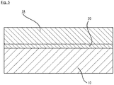
FIG. 5 is a schematic side view of a piezoelectric thin film according to a second embodiment. - Hereinafter, embodiments relating to thin films of piezoelectric bodies according to the present invention will be described with reference to the accompanying drawings. Note that, needless to say, the present invention is not limited to the following embodiments and the piezoelectric body may not be formed in a thin film shape.
-
FIG. 1 is a schematic side view of a piezoelectric thin film according to the present embodiment. As illustrated in this drawing, a piezoelectricthin film 1 is formed on asubstrate 10. The thickness of the piezoelectric thin film is not particularly limited. However, it is preferably within a range of 0.1 to 30 µm, and particularly preferably within a range of 0.1 to 2 µm for exhibiting excellent adhesion. - Note that the thickness, material, etc. of the
substrate 10 are not particularly limited as long as the piezoelectricthin film 1 can be formed on the surface of thesubstrate 10. Examples of thesubstrate 10 may include a silicon substrate, a heat resistant alloy substrate such as Inconel, and a resin film such as a polyimide. - The piezoelectric
thin film 1 is constituted by ytterbium (Yb)-doped aluminum nitride, which is represented by a chemical formula Al1-xYbxN where a value of x is more than 0 and less than 0.37, and has a lattice constant ratio c/a within a range of 1.53 or more and less than 1.6. The piezoelectric thin film with such a configuration has a greater piezoelectric coefficient d33 or g33 than piezoelectric thin films of aluminum nitride not doped with ytterbium. - Further, in the aforementioned chemical formula, the value of x is preferably within a range of more than 0.27 and less than 0.37. The piezoelectric
thin film 1 with such a configuration has the greater piezoelectric coefficient d33 or g33. - Further, it is particularly preferable that, in the aforementioned chemical formula, the value of x is within a range of more than 0.27 and less than 0.37 and the lattice constant ratio c/a is within a range of 1.53 or more and 1.555 or less. The piezoelectric
thin film 1 with such a configuration has the particularly high piezoelectric coefficient d33 or g33. - On the other hand, in the aforementioned chemical formula, the value of x is preferably within a range of more than 0 and less than 0.1. The piezoelectric
thin film 1 with such a configuration has the greater piezoelectric coefficient d33 or g33 than aluminum nitride not doped with ytterbium, despite having been doped with less ytterbium. - Further, it is particularly preferable that, in the aforementioned chemical formula, the value of x is within a range of more than 0 and less than 0.1 and the lattice constant ratio c/a is within a range of 1.57 or more and less than 1.6. The piezoelectric
thin film 1 with such a configuration has the sufficiently high piezoelectric coefficient d33 or g33 despite having been doped with less ytterbium. - Furthermore, sensors using these piezoelectric
thin films 1 exhibit a low loss and can be operated in a wide band. As a result, portable devices that use the piezoelectric thin films can operate at high frequencies and are more compact and power efficient. Note that the configuration of the sensor is not particularly limited, and any known configuration of sensor is compatible for manufacturing. - Next, a method for producing the piezoelectric thin film according to the present embodiment will be described. The piezoelectric
thin film 1 can be produced using methods such as a sputtering method and a deposition method in the same manner as for a general piezoelectric thin film. Specifically, for example, it can be produced by a sputtering treatment in which an ytterbium target and an aluminum target are simultaneously sputtered on the substrate 10 (e.g., a silicon (Si) substrate) under a nitrogen gas (N2) atmosphere or a mixed atmosphere of nitrogen gas (N2) and argon gas (Ar) (with a gas pressure of 1 Pa or less). Note that an alloy containing ytterbium and aluminum in a specific ratio may be used as a target. - The apparatus, sputtering targets, etc. described below were used to produce a plurality of piezoelectric thin films of ytterbium-doped aluminum nitride. Each piezoelectric thin film formed on an n-type silicon substrate with a specific resistance of 0.02 Ωcm had a thickness of 0.4 to 1.5 µm.
- Sputtering apparatus: BC3263 (manufactured by ULVAC)
- Ytterbium sputtering target material (concentration: 99.999%)
- Aluminum sputtering target material (concentration: 99.999%)
- Gas: mixed gas of nitrogen (purity: 99.99995% or higher) and argon gas (purity: 99.9999% or higher) (mixing ratio 40:60)
- Substrate heating temperature: 300 to 600°C
- Film forming experiments were performed after the air pressure inside a sputtering chamber was reduced to a high vacuum state of 10-6 or lower using a vacuum pump. Further, the target surface was subjected to a cleaning treatment immediately after the installation of the targets and immediately before each film forming experiment in order to prevent contamination by impurities such as oxygen.
-
FIG. 2 shows the concentration of ytterbium (Yb), the lattice constant ratio (c/a), d33, the specific dielectric constant εr, and g33 of each piezoelectric thin film obtained. In this figure, the lattice constant ratio c/a was calculated using an X-ray diffractometer (SmartLab manufactured by Rigaku Corp.), and the piezoelectric coefficient d33 and capacitance were measured using a piezometer (PM300 manufactured by Piezotest Pte Ltd.). These values were used to calculate the specific dielectric constant εr and g33. Note that the Yb concentration (x) was obtained by taking the average of measurements at 5 or more points in each sample using an EDX device (an energy dispersive X-ray spectrometer EX-420, manufactured by Horiba, Ltd.) inside a scanning electron microscope (S-4300 manufactured by Hitachi High-Tech Corp.). An error of x in the measurement was about ±0.003. - Further, a graph showing the relation between the concentration x of ytterbium and the piezoelectric coefficient d33 is shown in
FIG. 3 and a graph showing the relation between the lattice constant ratio (c/a) and the piezoelectric coefficient d33 is shown inFIG. 4 . - In the graphs, square plotted points indicate results of aluminum nitride not doped with ytterbium, circle plotted points indicate results of Examples, and triangle plotted points indicate results of Comparative examples.
- As evident from these graphs, it was found that the piezoelectric coefficient d33 of the piezoelectric thin film in which the value of x in the aforementioned chemical formula was more than 0 and less than 0.37 and the lattice constant ratio c/a was in a range of 1.53 or more and less than 1.6 was greater than that of the piezoelectric thin film of aluminum nitride not doped with ytterbium.
- Further, the graph shows that the piezoelectric thin film in which the value of x in the aforementioned chemical formula was in a range of more than 0.27 and less than 0.37 and the lattice constant ratio c/a was in a range of 1.53 or more and 1.555 or less had the particularly high piezoelectric coefficient d33.
- Further, the graph shows that the piezoelectric thin film in which the value of x was in a range of more than 0 and less than 0.1 and the lattice constant ratio c/a was in a range of 1.57 or more and less than 1.6 had the sufficiently high piezoelectric coefficient d33 despite having been doped with less ytterbium.
- In the aforementioned first embodiment, the piezoelectric thin film was produced directly on the substrate. However, the present invention is not limited thereto. For example, as shown in
FIG. 5 , anintermediate layer 20 may be disposed between thesubstrate 10 and a piezoelectricthin film 1A. - In this configuration, the material, the thickness, etc. of the
intermediate layer 20 are not particularly limited as long as the piezoelectricthin film 1A can be formed on theintermediate layer 20. Examples of the intermediate layer may include layers having a thickness of 50 to 200 nm constituted by aluminum nitride (AIN), gallium nitride (GaN), indium nitride (InN), titanium nitride (TiN), scandium nitride (ScN), ytterbium nitride (YbN), molybdenum (Mo), tungsten (W), hafnium (Hf), titanium (Ti), ruthenium (Ru), ruthenium oxide (RuO2), chromium (Cr), chromium nitride, platinum (Pt), gold (Au), silver (Ag), copper (Cu), aluminum (Al), tantalum (Ta), iridium (Ir), palladium (Pd), and nickel (Ni). - Disposing a layer like the
intermediate layer 20 on thesubstrate 10 improves the crystallinity (degree of crystallization) of the piezoelectric thin film. Thus, the piezoelectric thin film of ytterbium-doped aluminum nitride can have the further greater piezoelectric coefficients d33 or g33 than those not doped with ytterbium. - In the aforementioned second embodiment, the piezoelectric thin film was formed directly on the intermediate layer. However, the present invention is not limited thereto. For example, a diffusion layer may be further disposed between the intermediate layer and the piezoelectric thin film. The diffusion layer includes a substance a substance constituting the intermediate layer and a substance constituting the piezoelectric thin film. Note that the diffusion layer can be formed by, for example, forming the piezoelectric thin film on the intermediate layer and then heating the resulting product. The same effects as that in the second embodiment can be obtained when the diffusion layer is disposed in this manner.
-
- 1, 1A
- piezoelectric thin film
- 10
- substrate
- 20
- diffusion layer
Claims (9)
- A piezoelectric body represented by a chemical formula Al1-xYbxN where a value of x is more than 0 and less than 0.37 and having a lattice constant ratio c/a in a range of 1.53 or more and less than 1.6.
- The piezoelectric body according to claim 1, wherein the value of x is within a range of more than 0.27 and less than 0.37.
- The piezoelectric body according to claim 2, wherein the lattice constant ratio c/a is within a range of 1.53 or more and 1.555 or less.
- The piezoelectric body according to claim 1, wherein the value of x is within a range of more than 0 and less than 0.1.
- The piezoelectric body according to claim 4, wherein the lattice constant ratio c/a is within a range of 1.57 or more and less than 1.6.
- A piezoelectric body wherein the piezoelectric body according to any one of claims 1 to 5 is disposed on a substrate, and at least an intermediate layer is disposed between the piezoelectric body and the substrate.
- The piezoelectric body according to claim 6, wherein the intermediate layer includes at least one of aluminum nitride, gallium nitride, indium nitride, titanium nitride, scandium nitride, ytterbium nitride, molybdenum, tungsten, hafnium, titanium, ruthenium, ruthenium oxide, chromium, chromium nitride, platinum, gold, silver, copper, aluminum, tantalum, iridium, palladium, and nickel.
- The piezoelectric body according to claim 6 or 7, wherein a diffusion layer is further disposed between the intermediate layer and the piezoelectric body, the diffusion layer including a substance constituting the intermediate layer and a substance constituting the piezoelectric body.
- A MEMS devise using the piezoelectric body according to any one of claims 1 to 8.
Applications Claiming Priority (2)
| Application Number | Priority Date | Filing Date | Title |
|---|---|---|---|
| JP2018231681A JP7085208B2 (en) | 2018-12-11 | 2018-12-11 | Piezoelectric material and MEMS device using it |
| PCT/JP2019/046052 WO2020121796A1 (en) | 2018-12-11 | 2019-11-26 | Piezoelectric body and mems device using same |
Publications (4)
| Publication Number | Publication Date |
|---|---|
| EP3896029A1 true EP3896029A1 (en) | 2021-10-20 |
| EP3896029A4 EP3896029A4 (en) | 2022-11-02 |
| EP3896029B1 EP3896029B1 (en) | 2023-08-23 |
| EP3896029C0 EP3896029C0 (en) | 2023-08-23 |
Family
ID=71075954
Family Applications (1)
| Application Number | Title | Priority Date | Filing Date |
|---|---|---|---|
| EP19897007.1A Active EP3896029B1 (en) | 2018-12-11 | 2019-11-26 | Piezoelectric body and mems device using same |
Country Status (6)
| Country | Link |
|---|---|
| US (1) | US11968902B2 (en) |
| EP (1) | EP3896029B1 (en) |
| JP (1) | JP7085208B2 (en) |
| KR (1) | KR102604213B1 (en) |
| CN (1) | CN113165865B (en) |
| WO (1) | WO2020121796A1 (en) |
Cited By (1)
| Publication number | Priority date | Publication date | Assignee | Title |
|---|---|---|---|---|
| EP3865456A4 (en) * | 2019-02-22 | 2022-07-20 | National Institute Of Advanced Industrial Science And Technology | NITRIDE PIEZOELECTRIC BODY AND MEMS DEVICE USING THE SAME |
Family Cites Families (12)
| Publication number | Priority date | Publication date | Assignee | Title |
|---|---|---|---|---|
| JP4478910B2 (en) * | 2001-05-11 | 2010-06-09 | 宇部興産株式会社 | Piezoelectric thin film resonator |
| WO2002093740A1 (en) | 2001-05-11 | 2002-11-21 | Ube Electronics, Ltd. | Film bulk acoustic resonator |
| CN1983464B (en) * | 2002-10-24 | 2010-12-08 | 精工爱普生株式会社 | Ferroelectric film, ferroelectric capacitor, ferroelectric memory, piezoelectric element, semiconductor element |
| JP2005244184A (en) * | 2004-01-28 | 2005-09-08 | Toshiba Corp | Thin film piezoelectric element and method for manufacturing thin film piezoelectric element |
| JP4911907B2 (en) * | 2005-03-25 | 2012-04-04 | 京セラ株式会社 | Piezoelectric actuator and liquid ejection device |
| JP4977380B2 (en) * | 2005-05-31 | 2012-07-18 | 京セラ株式会社 | Piezoelectric actuator, driving method thereof, and print head |
| JP5190841B2 (en) | 2007-05-31 | 2013-04-24 | 独立行政法人産業技術総合研究所 | Piezoelectric thin film, piezoelectric body and manufacturing method thereof, and piezoelectric resonator, actuator element, and physical sensor using the piezoelectric thin film |
| TWI621185B (en) * | 2011-12-01 | 2018-04-11 | 半導體能源研究所股份有限公司 | Semiconductor device and method of manufacturing semiconductor device |
| US9520855B2 (en) * | 2014-02-26 | 2016-12-13 | Avago Technologies General Ip (Singapore) Pte. Ltd. | Bulk acoustic wave resonators having doped piezoelectric material and frame elements |
| US20170263847A1 (en) * | 2016-03-09 | 2017-09-14 | Teledyne Dalsa Semiconductor, Inc. | Piezoelectric Alloy Films |
| JP2017201050A (en) * | 2016-05-06 | 2017-11-09 | 学校法人早稲田大学 | Piezoelectric thin film and piezoelectric element using the same |
| JP7345855B2 (en) * | 2020-02-27 | 2023-09-19 | 国立研究開発法人産業技術総合研究所 | Nitride materials, piezoelectric bodies made of the same, and MEMS devices using the piezoelectric bodies |
-
2018
- 2018-12-11 JP JP2018231681A patent/JP7085208B2/en active Active
-
2019
- 2019-11-26 WO PCT/JP2019/046052 patent/WO2020121796A1/en not_active Ceased
- 2019-11-26 KR KR1020217008026A patent/KR102604213B1/en active Active
- 2019-11-26 EP EP19897007.1A patent/EP3896029B1/en active Active
- 2019-11-26 CN CN201980076704.8A patent/CN113165865B/en active Active
- 2019-11-26 US US17/276,464 patent/US11968902B2/en active Active
Cited By (2)
| Publication number | Priority date | Publication date | Assignee | Title |
|---|---|---|---|---|
| EP3865456A4 (en) * | 2019-02-22 | 2022-07-20 | National Institute Of Advanced Industrial Science And Technology | NITRIDE PIEZOELECTRIC BODY AND MEMS DEVICE USING THE SAME |
| US11999615B2 (en) | 2019-02-22 | 2024-06-04 | National Institute Of Advanced Industrial Science And Technology | Nitride piezoelectric body and MEMS device using same |
Also Published As
| Publication number | Publication date |
|---|---|
| US20220037582A1 (en) | 2022-02-03 |
| WO2020121796A1 (en) | 2020-06-18 |
| US11968902B2 (en) | 2024-04-23 |
| CN113165865A (en) | 2021-07-23 |
| EP3896029B1 (en) | 2023-08-23 |
| EP3896029A4 (en) | 2022-11-02 |
| KR102604213B1 (en) | 2023-11-20 |
| JP2020096040A (en) | 2020-06-18 |
| CN113165865B (en) | 2024-05-14 |
| JP7085208B2 (en) | 2022-06-16 |
| EP3896029C0 (en) | 2023-08-23 |
| KR20210048513A (en) | 2021-05-03 |
Similar Documents
| Publication | Publication Date | Title |
|---|---|---|
| Mertin et al. | Piezoelectric and structural properties of c-axis textured aluminium scandium nitride thin films up to high scandium content | |
| CN101325240B (en) | Piezoelectric thin film, piezoelectric material, and fabrication method of piezoelectric thin film and piezoelectric material, and piezoelectric resonator | |
| US10637435B2 (en) | Bulk acoustic wave resonator and filter including the same | |
| CN111244263B (en) | Piezoelectric thin film element | |
| US7758979B2 (en) | Piezoelectric thin film, piezoelectric material, and fabrication method of piezoelectric thin film and piezoelectric material, and piezoelectric resonator, actuator element, and physical sensor using piezoelectric thin film | |
| CN101322258B (en) | Piezoelectric element and method for manufacturing the same | |
| CN107112977B (en) | Piezoelectric film and piezoelectric resonator | |
| Mertin et al. | Enhanced piezoelectric properties of c-axis textured aluminium scandium nitride thin films with high scandium content: Influence of intrinsic stress and sputtering parameters | |
| US10009007B2 (en) | Bulk acoustic wave resonator with a molybdenum tantalum alloy electrode and filter including the same | |
| EP3216894A1 (en) | Piezoelectric alloy films | |
| US11558031B2 (en) | Film bulk acoustic resonator and method of manufacturing the same | |
| EP3896029B1 (en) | Piezoelectric body and mems device using same | |
| CN114341053B (en) | Nitride piezoelectric body and MEMS device using the same | |
| TWI904882B (en) | Nitride materials and piezoelectrics made therefrom, MEMS devices using the piezoelectrics, and strong dielectric materials and strong dielectrics made therefrom, and electronic components using the strong dielectrics. | |
| CN113226982B (en) | Nitride piezoelectric body and MEMS device using the same | |
| Lin et al. | Growth of highly c-axis oriented AlN films on 3C–SiC/Si substrate | |
| CN120898558A (en) | Piezoelectric elements and MEMS devices using such piezoelectric elements |
Legal Events
| Date | Code | Title | Description |
|---|---|---|---|
| STAA | Information on the status of an ep patent application or granted ep patent |
Free format text: STATUS: THE INTERNATIONAL PUBLICATION HAS BEEN MADE |
|
| PUAI | Public reference made under article 153(3) epc to a published international application that has entered the european phase |
Free format text: ORIGINAL CODE: 0009012 |
|
| STAA | Information on the status of an ep patent application or granted ep patent |
Free format text: STATUS: REQUEST FOR EXAMINATION WAS MADE |
|
| 17P | Request for examination filed |
Effective date: 20210414 |
|
| AK | Designated contracting states |
Kind code of ref document: A1 Designated state(s): AL AT BE BG CH CY CZ DE DK EE ES FI FR GB GR HR HU IE IS IT LI LT LU LV MC MK MT NL NO PL PT RO RS SE SI SK SM TR |
|
| DAV | Request for validation of the european patent (deleted) | ||
| DAX | Request for extension of the european patent (deleted) | ||
| A4 | Supplementary search report drawn up and despatched |
Effective date: 20220929 |
|
| RIC1 | Information provided on ipc code assigned before grant |
Ipc: H01L 41/08 20060101ALI20220923BHEP Ipc: H01L 41/187 20060101AFI20220923BHEP |
|
| REG | Reference to a national code |
Ref country code: DE Ref legal event code: R079 Free format text: PREVIOUS MAIN CLASS: B81B0003000000 Ipc: H10N0030000000 Ref document number: 602019035857 Country of ref document: DE |
|
| GRAP | Despatch of communication of intention to grant a patent |
Free format text: ORIGINAL CODE: EPIDOSNIGR1 |
|
| STAA | Information on the status of an ep patent application or granted ep patent |
Free format text: STATUS: GRANT OF PATENT IS INTENDED |
|
| RIC1 | Information provided on ipc code assigned before grant |
Ipc: H10N 30/853 20230101ALI20230224BHEP Ipc: H10N 30/00 20230101AFI20230224BHEP |
|
| INTG | Intention to grant announced |
Effective date: 20230329 |
|
| RIN1 | Information on inventor provided before grant (corrected) |
Inventor name: HIRATA KENJI Inventor name: ANGGRAINI SRI AYU Inventor name: AKIYAMA MORITO Inventor name: YAMADA HIROSHI Inventor name: UEHARA MASATO |
|
| GRAS | Grant fee paid |
Free format text: ORIGINAL CODE: EPIDOSNIGR3 |
|
| GRAA | (expected) grant |
Free format text: ORIGINAL CODE: 0009210 |
|
| STAA | Information on the status of an ep patent application or granted ep patent |
Free format text: STATUS: THE PATENT HAS BEEN GRANTED |
|
| AK | Designated contracting states |
Kind code of ref document: B1 Designated state(s): AL AT BE BG CH CY CZ DE DK EE ES FI FR GB GR HR HU IE IS IT LI LT LU LV MC MK MT NL NO PL PT RO RS SE SI SK SM TR |
|
| REG | Reference to a national code |
Ref country code: GB Ref legal event code: FG4D |
|
| REG | Reference to a national code |
Ref country code: CH Ref legal event code: EP |
|
| REG | Reference to a national code |
Ref country code: IE Ref legal event code: FG4D |
|
| REG | Reference to a national code |
Ref country code: DE Ref legal event code: R096 Ref document number: 602019035857 Country of ref document: DE |
|
| U01 | Request for unitary effect filed |
Effective date: 20230823 |
|
| U07 | Unitary effect registered |
Designated state(s): AT BE BG DE DK EE FI FR IT LT LU LV MT NL PT SE SI Effective date: 20230828 |
|
| U20 | Renewal fee for the european patent with unitary effect paid |
Year of fee payment: 5 Effective date: 20230919 |
|
| PG25 | Lapsed in a contracting state [announced via postgrant information from national office to epo] |
Ref country code: GR Free format text: LAPSE BECAUSE OF FAILURE TO SUBMIT A TRANSLATION OF THE DESCRIPTION OR TO PAY THE FEE WITHIN THE PRESCRIBED TIME-LIMIT Effective date: 20231124 |
|
| PG25 | Lapsed in a contracting state [announced via postgrant information from national office to epo] |
Ref country code: IS Free format text: LAPSE BECAUSE OF FAILURE TO SUBMIT A TRANSLATION OF THE DESCRIPTION OR TO PAY THE FEE WITHIN THE PRESCRIBED TIME-LIMIT Effective date: 20231223 |
|
| PG25 | Lapsed in a contracting state [announced via postgrant information from national office to epo] |
Ref country code: RS Free format text: LAPSE BECAUSE OF FAILURE TO SUBMIT A TRANSLATION OF THE DESCRIPTION OR TO PAY THE FEE WITHIN THE PRESCRIBED TIME-LIMIT Effective date: 20230823 Ref country code: NO Free format text: LAPSE BECAUSE OF FAILURE TO SUBMIT A TRANSLATION OF THE DESCRIPTION OR TO PAY THE FEE WITHIN THE PRESCRIBED TIME-LIMIT Effective date: 20231123 Ref country code: IS Free format text: LAPSE BECAUSE OF FAILURE TO SUBMIT A TRANSLATION OF THE DESCRIPTION OR TO PAY THE FEE WITHIN THE PRESCRIBED TIME-LIMIT Effective date: 20231223 Ref country code: HR Free format text: LAPSE BECAUSE OF FAILURE TO SUBMIT A TRANSLATION OF THE DESCRIPTION OR TO PAY THE FEE WITHIN THE PRESCRIBED TIME-LIMIT Effective date: 20230823 Ref country code: GR Free format text: LAPSE BECAUSE OF FAILURE TO SUBMIT A TRANSLATION OF THE DESCRIPTION OR TO PAY THE FEE WITHIN THE PRESCRIBED TIME-LIMIT Effective date: 20231124 |
|
| PG25 | Lapsed in a contracting state [announced via postgrant information from national office to epo] |
Ref country code: PL Free format text: LAPSE BECAUSE OF FAILURE TO SUBMIT A TRANSLATION OF THE DESCRIPTION OR TO PAY THE FEE WITHIN THE PRESCRIBED TIME-LIMIT Effective date: 20230823 |
|
| PG25 | Lapsed in a contracting state [announced via postgrant information from national office to epo] |
Ref country code: ES Free format text: LAPSE BECAUSE OF FAILURE TO SUBMIT A TRANSLATION OF THE DESCRIPTION OR TO PAY THE FEE WITHIN THE PRESCRIBED TIME-LIMIT Effective date: 20230823 |
|
| PG25 | Lapsed in a contracting state [announced via postgrant information from national office to epo] |
Ref country code: SM Free format text: LAPSE BECAUSE OF FAILURE TO SUBMIT A TRANSLATION OF THE DESCRIPTION OR TO PAY THE FEE WITHIN THE PRESCRIBED TIME-LIMIT Effective date: 20230823 Ref country code: RO Free format text: LAPSE BECAUSE OF FAILURE TO SUBMIT A TRANSLATION OF THE DESCRIPTION OR TO PAY THE FEE WITHIN THE PRESCRIBED TIME-LIMIT Effective date: 20230823 Ref country code: ES Free format text: LAPSE BECAUSE OF FAILURE TO SUBMIT A TRANSLATION OF THE DESCRIPTION OR TO PAY THE FEE WITHIN THE PRESCRIBED TIME-LIMIT Effective date: 20230823 Ref country code: CZ Free format text: LAPSE BECAUSE OF FAILURE TO SUBMIT A TRANSLATION OF THE DESCRIPTION OR TO PAY THE FEE WITHIN THE PRESCRIBED TIME-LIMIT Effective date: 20230823 Ref country code: SK Free format text: LAPSE BECAUSE OF FAILURE TO SUBMIT A TRANSLATION OF THE DESCRIPTION OR TO PAY THE FEE WITHIN THE PRESCRIBED TIME-LIMIT Effective date: 20230823 |
|
| REG | Reference to a national code |
Ref country code: DE Ref legal event code: R097 Ref document number: 602019035857 Country of ref document: DE |
|
| PLBE | No opposition filed within time limit |
Free format text: ORIGINAL CODE: 0009261 |
|
| STAA | Information on the status of an ep patent application or granted ep patent |
Free format text: STATUS: NO OPPOSITION FILED WITHIN TIME LIMIT |
|
| PG25 | Lapsed in a contracting state [announced via postgrant information from national office to epo] |
Ref country code: MC Free format text: LAPSE BECAUSE OF FAILURE TO SUBMIT A TRANSLATION OF THE DESCRIPTION OR TO PAY THE FEE WITHIN THE PRESCRIBED TIME-LIMIT Effective date: 20230823 |
|
| GBPC | Gb: european patent ceased through non-payment of renewal fee |
Effective date: 20231126 |
|
| 26N | No opposition filed |
Effective date: 20240524 |
|
| PG25 | Lapsed in a contracting state [announced via postgrant information from national office to epo] |
Ref country code: MC Free format text: LAPSE BECAUSE OF FAILURE TO SUBMIT A TRANSLATION OF THE DESCRIPTION OR TO PAY THE FEE WITHIN THE PRESCRIBED TIME-LIMIT Effective date: 20230823 |
|
| REG | Reference to a national code |
Ref country code: IE Ref legal event code: MM4A |
|
| PG25 | Lapsed in a contracting state [announced via postgrant information from national office to epo] |
Ref country code: IE Free format text: LAPSE BECAUSE OF NON-PAYMENT OF DUE FEES Effective date: 20231126 |
|
| PG25 | Lapsed in a contracting state [announced via postgrant information from national office to epo] |
Ref country code: GB Free format text: LAPSE BECAUSE OF NON-PAYMENT OF DUE FEES Effective date: 20231126 |
|
| PG25 | Lapsed in a contracting state [announced via postgrant information from national office to epo] |
Ref country code: IE Free format text: LAPSE BECAUSE OF NON-PAYMENT OF DUE FEES Effective date: 20231126 Ref country code: GB Free format text: LAPSE BECAUSE OF NON-PAYMENT OF DUE FEES Effective date: 20231126 |
|
| U20 | Renewal fee for the european patent with unitary effect paid |
Year of fee payment: 6 Effective date: 20241122 |
|
| PG25 | Lapsed in a contracting state [announced via postgrant information from national office to epo] |
Ref country code: CY Free format text: LAPSE BECAUSE OF FAILURE TO SUBMIT A TRANSLATION OF THE DESCRIPTION OR TO PAY THE FEE WITHIN THE PRESCRIBED TIME-LIMIT; INVALID AB INITIO Effective date: 20191126 |
|
| PG25 | Lapsed in a contracting state [announced via postgrant information from national office to epo] |
Ref country code: HU Free format text: LAPSE BECAUSE OF FAILURE TO SUBMIT A TRANSLATION OF THE DESCRIPTION OR TO PAY THE FEE WITHIN THE PRESCRIBED TIME-LIMIT; INVALID AB INITIO Effective date: 20191126 |
|
| REG | Reference to a national code |
Ref country code: CH Ref legal event code: U11 Free format text: ST27 STATUS EVENT CODE: U-0-0-U10-U11 (AS PROVIDED BY THE NATIONAL OFFICE) Effective date: 20251201 |
|
| PG25 | Lapsed in a contracting state [announced via postgrant information from national office to epo] |
Ref country code: TR Free format text: LAPSE BECAUSE OF FAILURE TO SUBMIT A TRANSLATION OF THE DESCRIPTION OR TO PAY THE FEE WITHIN THE PRESCRIBED TIME-LIMIT Effective date: 20230823 |
|
| U20 | Renewal fee for the european patent with unitary effect paid |
Year of fee payment: 7 Effective date: 20251124 |
|
| PGFP | Annual fee paid to national office [announced via postgrant information from national office to epo] |
Ref country code: CH Payment date: 20251201 Year of fee payment: 7 |