EP3893493A1 - Signal processing device, electronic device, and signal processing method and program - Google Patents
Signal processing device, electronic device, and signal processing method and program Download PDFInfo
- Publication number
- EP3893493A1 EP3893493A1 EP19893042.2A EP19893042A EP3893493A1 EP 3893493 A1 EP3893493 A1 EP 3893493A1 EP 19893042 A EP19893042 A EP 19893042A EP 3893493 A1 EP3893493 A1 EP 3893493A1
- Authority
- EP
- European Patent Office
- Prior art keywords
- packets
- buffer memory
- signal processing
- event
- processing device
- Prior art date
- Legal status (The legal status is an assumption and is not a legal conclusion. Google has not performed a legal analysis and makes no representation as to the accuracy of the status listed.)
- Granted
Links
Images



Classifications
-
- H—ELECTRICITY
- H04—ELECTRIC COMMUNICATION TECHNIQUE
- H04N—PICTORIAL COMMUNICATION, e.g. TELEVISION
- H04N23/00—Cameras or camera modules comprising electronic image sensors; Control thereof
- H04N23/80—Camera processing pipelines; Components thereof
-
- H—ELECTRICITY
- H04—ELECTRIC COMMUNICATION TECHNIQUE
- H04N—PICTORIAL COMMUNICATION, e.g. TELEVISION
- H04N25/00—Circuitry of solid-state image sensors [SSIS]; Control thereof
- H04N25/47—Image sensors with pixel address output; Event-driven image sensors; Selection of pixels to be read out based on image data
-
- H—ELECTRICITY
- H04—ELECTRIC COMMUNICATION TECHNIQUE
- H04N—PICTORIAL COMMUNICATION, e.g. TELEVISION
- H04N25/00—Circuitry of solid-state image sensors [SSIS]; Control thereof
- H04N25/50—Control of the SSIS exposure
-
- H—ELECTRICITY
- H04—ELECTRIC COMMUNICATION TECHNIQUE
- H04N—PICTORIAL COMMUNICATION, e.g. TELEVISION
- H04N25/00—Circuitry of solid-state image sensors [SSIS]; Control thereof
- H04N25/70—SSIS architectures; Circuits associated therewith
- H04N25/703—SSIS architectures incorporating pixels for producing signals other than image signals
- H04N25/707—Pixels for event detection
-
- H—ELECTRICITY
- H04—ELECTRIC COMMUNICATION TECHNIQUE
- H04N—PICTORIAL COMMUNICATION, e.g. TELEVISION
- H04N25/00—Circuitry of solid-state image sensors [SSIS]; Control thereof
- H04N25/70—SSIS architectures; Circuits associated therewith
- H04N25/71—Charge-coupled device [CCD] sensors; Charge-transfer registers specially adapted for CCD sensors
- H04N25/75—Circuitry for providing, modifying or processing image signals from the pixel array
-
- H—ELECTRICITY
- H04—ELECTRIC COMMUNICATION TECHNIQUE
- H04N—PICTORIAL COMMUNICATION, e.g. TELEVISION
- H04N25/00—Circuitry of solid-state image sensors [SSIS]; Control thereof
- H04N25/70—SSIS architectures; Circuits associated therewith
- H04N25/76—Addressed sensors, e.g. MOS or CMOS sensors
- H04N25/77—Pixel circuitry, e.g. memories, A/D converters, pixel amplifiers, shared circuits or shared components
- H04N25/771—Pixel circuitry, e.g. memories, A/D converters, pixel amplifiers, shared circuits or shared components comprising storage means other than floating diffusion
Definitions
- the present invention relates to a signal processing device, electronic equipment, a signal processing method, and a program.
- An event-driven vision sensor in which a pixel that has detected a change in the intensity of incident light generates a signal asynchronously in time has been known.
- the event-driven vision sensor is advantageous in that a low-power and high-speed operation can be performed as compared to a frame-type vision sensor, specifically, an image sensor such as a CCD (charge Coupled Device) or a CMOS (Complementary Metal Oxide Semiconductor) that scans all pixels in each predetermined cycle.
- CCD Charge Coupled Device
- CMOS Complementary Metal Oxide Semiconductor
- an AER Address Event Representation
- the AER format for example, four pieces of data of an x coordinate and a y coordinate of a pixel in which an event has occurred, ON/OFF (polarity) of the event, and a time stamp are transferred.
- a signal processing device including a communication unit which receives packets transmitted from an event-driven vision sensor including a sensor array including sensors generating event signals when a change in intensity of incident light is detected, a buffer memory in which the packets are temporarily stored, and a readout control unit which forcibly reads out the packets from the buffer memory in a case in which predetermined conditions are satisfied.
- electronic equipment including the above signal processing device is provided.
- a signal processing method including a step of receiving packets transmitted from an event-driven vision sensor including a sensor array including sensors generating event signals when a change in intensity of incident light is detected, a step of temporarily storing the packets in a buffer memory, and a step of forcibly reading out the packets from the buffer memory in a case in which predetermined conditions are satisfied.
- a program which allows a processing circuit of a signal processing device to execute a step of temporarily storing packets, in a buffer memory, transmitted from an event-driven vision sensor including a sensor array including sensors generating event signals when a change in the intensity of incident light is detected, and a step of forcibly reading out the packets from the buffer memory in a case in which predetermined conditions are satisfied.
- the packets are forcibly read out from the buffer memory in a case in which the predetermined conditions are satisfied, it is possible to suppress the processing delay of the data output from the event-driven vision sensor.
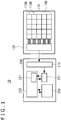
- Fig. 1 is a block diagram illustrating a schematic configuration of electronic equipment according to a first embodiment of the present invention.
- electronic equipment 10 includes an event-driven vision sensor 100 and a control unit 200.
- the vision sensor 100 includes a sensor array 110 including sensors 110A, 110B, and the like corresponding to pixels of an image, and a processing circuit 120 connected to the sensor array 110.
- the sensors 110A, 110B, and the like include light receiving elements, and generate event signals when detecting a change in the intensity of incident light, more specifically, a change in luminance.
- the event signal is output from the processing circuit 120 as information indicating, for example, a time stamp, identification information (for example, the position of the pixel) of the sensor, and the polarity (increase or decrease) of a change in luminance.
- the processing circuit 120 adds a transfer end packet to the packets of the event signals.
- the intensity of light reflected or scattered by the subject changes, and thus, the movement of the subject can be detected in time series by the event signals generated by the sensors 110A, 110B, and the like corresponding to, for example, the edge of the subject.
- the control unit 200 includes a communication interface 210, a processing circuit 220, and a memory 230.
- the communication interface 210 receives packets transmitted from the processing circuit 120 of the vision sensor 100.
- the packets are temporarily stored in a buffer memory 231.
- the processing circuit 220 operates in accordance with, for example, a program stored in the memory 230, and processes packets read out from the buffer memory 231.
- the processing circuit 220 generates an image in which the positions where changes in luminance have occurred are mapped in time series on the basis of the event signals included in the packets, and temporarily or continuously stores the image in the memory 230 or further transmits the image to another device via the communication interface 210.
- the processing circuit 220 includes a readout control unit 221 that forcibly reads out the packets from the buffer memory 231 when predetermined conditions are satisfied.
- Fig. 2A to Fig. 2C are diagrams each conceptually describing the transfer end packet in the first embodiment of the present invention.
- the minimum unit (one packet) of the event signal output from the vision sensor 100 is four bytes
- a the size of the buffer memory 231 in the control unit 200 is 64 bytes (corresponding to 16 packets).
- the readout control unit 221 is configured to read out packets 121 from the buffer memory 231 when the capacity of the buffer memory 231 becomes full.
- the readout control unit 221 does not read out the packets 121 from the buffer memory 231. This situation continues until the capacity of the buffer memory 231 becomes full due to the event signals received thereafter or until the packets 121 are forcibly read out from the buffer memory 231 due to timeout. Accordingly, there is a possibility that a delay occurs between the generation of the event signal by the vision sensor 100 and the processing of the event signal by the processing circuit 220.
- the situation as described above occurs because the event signal is generated asynchronously in time in the event-driven vision sensor 100.
- the sensors 110A, 110B, and the like configuring the sensor array 110 in the vision sensor 100 only the sensor that has detected a change in luminance generates the event signal, and the sensor that has not detected a change in luminance does not generate the event signal, so that a low-power and high-speed operation can be performed as compared to a frame-type vision sensor.
- the vision sensor 100 the amount of data transmitted per time varies, unlike the frame-type vision sensor which transmits data corresponding to all the pixels at the time of scanning, and accordingly, there is a possibility that the delay as described above may occur.
- the processing circuit 120 in the vision sensor 100 adds a transfer end packet 122 to the packets 121 of the event signals in the embodiment as in the examples illustrated in Fig. 2B and Fig. 2C . More specifically, when scanning of the sensors 110A, 110B, and the like is completed, the processing circuit 120 adds the transfer end packet 122 to the packets 121 of the event signals. In this case, when the transfer end packet 122 is stored in the buffer memory 231, the readout control unit 221 forcibly reads out the packets 121 from the buffer memory 231 irrespective of the free capacity of the buffer memory 231. In the example illustrated in Fig.
- the readout control unit 221 when finding the transfer end packet 122, stores padding data 123 in the free capacity of the buffer memory 231 to fill up the capacity of the buffer memory 231, and the packets 121 are accordingly sent to the process in the processing circuit 220.
- the readout control unit 221 when finding the transfer end packet 122, may be also configured to forcibly read out the packets 121 from the buffer memory 231 without padding and send the packets to the process in the processing circuit 220.
- Fig. 3 is a flowchart illustrating an example of a process of the processing circuit of the vision sensor in the first embodiment of the present invention.
- the processing circuit 120 executes scanning of the sensor array 110 (Step S101).
- the scanning of the sensor array 110 is executed by scanning the sensors 110A, 110B, and the like in a predetermined order and acquiring the event signal only from the sensor that has detected a change in luminance.
- the scanning of the event-driven vision sensor 100 is executed at a higher speed because a process for the sensor that has not detected a change in luminance is skipped.
- the processing circuit 120 adds the transfer end packet to the packets of the event signals (Step S102).
- the processing circuit 120 repeats these processes (Step S103) .
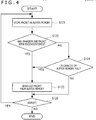
- Fig. 4 is a flowchart illustrating an example of a process of the readout control unit in the first embodiment of the present invention.
- the readout control unit 221 stores the packets of the event signals received from the vision sensor 100 in the buffer memory 231 (Step S121).
- the readout control unit 221 monitors the packets of the event signals stored in the buffer memory 231, and in a case in which the transfer end packet 122 is received or stored (Step S122), the packets 121 are read out from the buffer memory 231 (Step S123). Even in a case in which the capacity of the buffer memory 231 becomes full (Step S124), the readout control unit 221 reads out the packets 121 from the buffer memory 231 (Step S123) .
- the readout control unit 221 repeats these processes (Step S125).
- the packets 121 are sequentially read out from the buffer memory 231 by the process in Step S105 described above. If the transfer efficiency in a case in which the transmission amount is large as described above is considered, it is preferable that the capacity of the buffer memory 231 is large to some extent.
- the forcible readout is executed by the transfer end packet 122 as described above, so that the processing delay of the event signals in the control unit 200 can be suppressed to a time corresponding to one scan of the sensor array 110 at most while securing the capacity of the buffer memory 231.
- the processing circuit 120 of the vision sensor 100 adds a transfer start packet to the packets of the event signals in the same configuration of the electronic equipment as the above-described first embodiment.
- the process of the processing circuit 120 in the embodiment may be a process in which the order of Step S101 and Step S102 is switched and the transfer end packet is replaced with the transfer start packet in, for example, the example described above by using Fig. 3 .
- the configuration of the embodiment is the same as that of the above-described first embodiment, and thus, the duplicated and detailed description thereof is omitted.
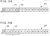
- Fig. 5A and Fig. 5B are diagrams each conceptually describing the transfer start packet in the second embodiment of the present invention.
- the buffer memory 231 is configured in the same manner as the examples described above with reference to Fig. 2A to Fig. 2C .
- Note that a case in which the transfer start packet is not received is the same as the example described with reference to Fig. 2A , and is accordingly omitted.
- the readout control unit 221 when a transfer start packet 124 is newly received, the readout control unit 221 forcibly reads out the packets 121 of the event signals stored in the buffer memory 121 at that time, and sends the packets 121 to the process in the processing circuit 220.
- the readout control unit 221 may perform the padding as in the example illustrated in Fig. 2B . In this case, the processing delay of the event signals in the control unit 200 is suppressed to a time corresponding to one scan of the sensor array 110 at most.
- the readout control unit 221 when the number of packets 121 of the event signals stored in the buffer memory 231 reaches a predetermined number n counted from the transfer start packet 124, the readout control unit 221 forcibly reads out the packets 121 of the event signals stored in the buffer memory 231 at that time, and sends the packets to the process in the processing circuit 220.
- the predetermined number n can be statistically determined as the mean value or the maximum value of the numbers of event signals output in one scan of the sensor array 110.
- the processing delay of the event signals in the control unit 200 can be suppressed while securing the capacity of the buffer memory 231 as similar to the above-described first embodiment.
- the embodiment can be also applied to, for example, a case in which the end of scanning is not specified in the processing circuit 120 because the event signals generated by the vision sensor 100 is asynchronous in time.
- the processing circuit 120 of the vision sensor 100 adds a delimiter (separator) packet such as the transfer end packet 122 or the transfer start packet 124 to the packets corresponding to the event signals, so that the processing delay of the event signals is prevented.
- a delimiter (separator) packet such as the transfer end packet 122 or the transfer start packet 124 to the packets corresponding to the event signals.
- the processing circuit 120 does not necessarily execute the scanning of the sensor array 110 as described above.
- the processing circuit 120 transmits the delimiter packet to the control unit 200 in each predetermined time cycle, and the readout control unit 221 handles the delimiter packet in the same manner as the transfer end packet 122 and the transfer start packet 124 in the above example, so that the processing delay of the event signals can be prevented.
- the processing circuit 120 of the vision sensor 100 does not add the delimiter packet to the packets of the event signals, and the readout control unit 221 of the control unit 200 forcibly reads out the packets 121 of the event signals stored in the buffer memory 231 in accordance with predetermined conditions, so that the processing delay of the event signals can be prevented.
- the configuration of the present embodiment is the same as that of the above-described first embodiment, and thus, the duplicated and detailed description thereof is omitted.
- Fig. 6 is a flowchart illustrating an example of a process of the readout control unit in the third embodiment of the present invention.
- the readout control unit 221 stores the packets of the event signals received from the vision sensor 100 in the buffer memory 231 (Step S301).
- the readout control unit 221 monitors the packets of the event signals stored in the buffer memory 231, and in a case in which the identification information (for example, the position of the pixel) of the sensor indicated by the event signal circulates (Step S302), the packets 121 are read out from the buffer memory 231 (Step S303) .
- Step S304 Even in a case in which the capacity of the buffer memory 231 becomes full (Step S304), the readout control unit 221 reads out the packets 121 from the buffer memory 231 (Step S303). The readout control unit 221 repeats these processes (Step S305) .
- the readout control unit 221 forcibly reads out the packets 121 from the buffer memory 231 on condition that the identification information of the sensor indicated by the event signal circulates.
- the readout control unit 221 may determine that the identification information circulates in a case in which an event signal indicating the same identification information associated with a different time stamp is received.
- the processing delay of the event signals in the control unit 200 can be suppressed while securing the capacity of the buffer memory 231 as similar to the above-described first embodiment and second embodiment.
- the present embodiment can be also applied to, for example, a case in which it is not easy to implement the function of adding the delimiter packet to the event signals in the processing circuit 120.
Landscapes
- Engineering & Computer Science (AREA)
- Multimedia (AREA)
- Signal Processing (AREA)
- Data Exchanges In Wide-Area Networks (AREA)
- Closed-Circuit Television Systems (AREA)
- Image Input (AREA)
- Studio Devices (AREA)
- Two-Way Televisions, Distribution Of Moving Picture Or The Like (AREA)
Abstract
Description
- The present invention relates to a signal processing device, electronic equipment, a signal processing method, and a program.
- An event-driven vision sensor in which a pixel that has detected a change in the intensity of incident light generates a signal asynchronously in time has been known. The event-driven vision sensor is advantageous in that a low-power and high-speed operation can be performed as compared to a frame-type vision sensor, specifically, an image sensor such as a CCD (charge Coupled Device) or a CMOS (Complementary Metal Oxide Semiconductor) that scans all pixels in each predetermined cycle. Techniques related to such an event-driven vision sensor are described in, for example,
PTL 1 andPTL 2. - As a method of transmitting an event signal generated by such an event-driven vision sensor, an AER (Address Event Representation) format has been known. In the AER format, for example, four pieces of data of an x coordinate and a y coordinate of a pixel in which an event has occurred, ON/OFF (polarity) of the event, and a time stamp are transferred.
-
- [PTL 1]
JP 2014-535098T - [PTL 2]
JP 2018-85725A - However, since signals are generated asynchronously in time in the event-driven vision sensor, an amount of data transmitted per time in the AER format varies, and thus, there has been a problem that the burst size of a buffer is not filled and a delay occurs in data processing.
- Therefore, an object of the present invention is to provide a signal processing device, electronic equipment, a signal processing method, and a program capable of eliminating a processing delay of data output from an event-driven vision sensor.
- According to one aspect of the present invention, provided is a signal processing device including a communication unit which receives packets transmitted from an event-driven vision sensor including a sensor array including sensors generating event signals when a change in intensity of incident light is detected, a buffer memory in which the packets are temporarily stored, and a readout control unit which forcibly reads out the packets from the buffer memory in a case in which predetermined conditions are satisfied.
According to another aspect of the present invention, electronic equipment including the above signal processing device is provided.
According to still another aspect of the present invention, provided is a signal processing method including a step of receiving packets transmitted from an event-driven vision sensor including a sensor array including sensors generating event signals when a change in intensity of incident light is detected, a step of temporarily storing the packets in a buffer memory, and a step of forcibly reading out the packets from the buffer memory in a case in which predetermined conditions are satisfied.
According to yet another aspect of the present invention, provided is a program which allows a processing circuit of a signal processing device to execute a step of temporarily storing packets, in a buffer memory, transmitted from an event-driven vision sensor including a sensor array including sensors generating event signals when a change in the intensity of incident light is detected, and a step of forcibly reading out the packets from the buffer memory in a case in which predetermined conditions are satisfied. - According to the above configuration, since the packets are forcibly read out from the buffer memory in a case in which the predetermined conditions are satisfied, it is possible to suppress the processing delay of the data output from the event-driven vision sensor.
-
- [
Fig. 1 ]
Fig. 1 is a block diagram illustrating a schematic configuration of electronic equipment according to a first embodiment of the present invention. - [
Fig. 2A ]
Fig. 2A is a diagram for conceptually describing a transfer end packet in the first embodiment of the present invention. - [
Fig. 2B ]
Fig. 2B is a diagram for conceptually describing the transfer end packet in the first embodiment of the present invention. - [
Fig. 2C ]
Fig. 2C is a diagram for conceptually describing the transfer end packet in the first embodiment of the present invention. - [
Fig. 3 ]
Fig. 3 is a flowchart illustrating an example of a process of a processing circuit of a vision sensor in the first embodiment of the present invention. - [
Fig. 4 ]
Fig. 4 is a flowchart illustrating an example of a process of a readout control unit in the first embodiment of the present invention. - [
Fig. 5A ]
Fig. 5A is a diagram for conceptually describing a transfer start packet in a second embodiment of the present invention. - [
Fig. 5B ]
Fig. 5B is a diagram for conceptually describing the transfer start packet in the second embodiment of the present invention. - [
Fig. 6 ]
Fig. 6 is a flowchart illustrating an example of a process of a readout control unit in a third embodiment of the present invention. - Hereinafter, several embodiments of the present invention will be described in detail with reference to the accompanying drawings. Note that constitutional elements having substantially the same functional configurations are denoted by the same reference signs in the specification and the drawings, and the duplicated description thereof is omitted.
-
Fig. 1 is a block diagram illustrating a schematic configuration of electronic equipment according to a first embodiment of the present invention. As illustrated inFig. 1 ,electronic equipment 10 includes an event-drivenvision sensor 100 and acontrol unit 200. - The
vision sensor 100 includes asensor array 110 includingsensors processing circuit 120 connected to thesensor array 110. Thesensors processing circuit 120 as information indicating, for example, a time stamp, identification information (for example, the position of the pixel) of the sensor, and the polarity (increase or decrease) of a change in luminance. As will be described later, theprocessing circuit 120 adds a transfer end packet to the packets of the event signals. When a subject moves within the angle of view of thesensor array 110, the intensity of light reflected or scattered by the subject changes, and thus, the movement of the subject can be detected in time series by the event signals generated by thesensors - The
control unit 200 includes acommunication interface 210, aprocessing circuit 220, and amemory 230. Thecommunication interface 210 receives packets transmitted from theprocessing circuit 120 of thevision sensor 100. The packets are temporarily stored in abuffer memory 231. Theprocessing circuit 220 operates in accordance with, for example, a program stored in thememory 230, and processes packets read out from thebuffer memory 231. For example, theprocessing circuit 220 generates an image in which the positions where changes in luminance have occurred are mapped in time series on the basis of the event signals included in the packets, and temporarily or continuously stores the image in thememory 230 or further transmits the image to another device via thecommunication interface 210. Here, theprocessing circuit 220 includes areadout control unit 221 that forcibly reads out the packets from thebuffer memory 231 when predetermined conditions are satisfied. -
Fig. 2A to Fig. 2C are diagrams each conceptually describing the transfer end packet in the first embodiment of the present invention. In the examples illustrated inFig. 2A to Fig. 2C , the minimum unit (one packet) of the event signal output from thevision sensor 100 is four bytes, a the size of thebuffer memory 231 in thecontrol unit 200 is 64 bytes (corresponding to 16 packets). - In the example illustrated in
Fig. 2A , thereadout control unit 221 is configured to read outpackets 121 from thebuffer memory 231 when the capacity of thebuffer memory 231 becomes full. Here, in a case in which the number of events detected by thesensor array 110 is small and thevision sensor 100 outputs only the event signals corresponding to five packets, that is, 20 bytes, the capacity of thebuffer memory 231 is still available. Therefore, thereadout control unit 221 does not read out thepackets 121 from thebuffer memory 231. This situation continues until the capacity of thebuffer memory 231 becomes full due to the event signals received thereafter or until thepackets 121 are forcibly read out from thebuffer memory 231 due to timeout. Accordingly, there is a possibility that a delay occurs between the generation of the event signal by thevision sensor 100 and the processing of the event signal by theprocessing circuit 220. - The situation as described above occurs because the event signal is generated asynchronously in time in the event-driven
vision sensor 100. Among thesensors sensor array 110 in thevision sensor 100, only the sensor that has detected a change in luminance generates the event signal, and the sensor that has not detected a change in luminance does not generate the event signal, so that a low-power and high-speed operation can be performed as compared to a frame-type vision sensor. In contrast, in thevision sensor 100, the amount of data transmitted per time varies, unlike the frame-type vision sensor which transmits data corresponding to all the pixels at the time of scanning, and accordingly, there is a possibility that the delay as described above may occur. - Thus, the
processing circuit 120 in thevision sensor 100 adds atransfer end packet 122 to thepackets 121 of the event signals in the embodiment as in the examples illustrated inFig. 2B and Fig. 2C . More specifically, when scanning of thesensors processing circuit 120 adds thetransfer end packet 122 to thepackets 121 of the event signals. In this case, when thetransfer end packet 122 is stored in thebuffer memory 231, thereadout control unit 221 forcibly reads out thepackets 121 from thebuffer memory 231 irrespective of the free capacity of thebuffer memory 231. In the example illustrated inFig. 2B , when finding thetransfer end packet 122, thereadout control unit 221stores padding data 123 in the free capacity of thebuffer memory 231 to fill up the capacity of thebuffer memory 231, and thepackets 121 are accordingly sent to the process in theprocessing circuit 220. In addition, in the example illustrated inFig. 2C , when finding thetransfer end packet 122, thereadout control unit 221 may be also configured to forcibly read out thepackets 121 from thebuffer memory 231 without padding and send the packets to the process in theprocessing circuit 220. -
Fig. 3 is a flowchart illustrating an example of a process of the processing circuit of the vision sensor in the first embodiment of the present invention. In the illustrated example, theprocessing circuit 120 executes scanning of the sensor array 110 (Step S101). Here, the scanning of thesensor array 110 is executed by scanning thesensors vision sensor 100 is executed at a higher speed because a process for the sensor that has not detected a change in luminance is skipped. When the scanning in Step S101 is completed, theprocessing circuit 120 adds the transfer end packet to the packets of the event signals (Step S102). Theprocessing circuit 120 repeats these processes (Step S103) . -
Fig. 4 is a flowchart illustrating an example of a process of the readout control unit in the first embodiment of the present invention. In the illustrated example, thereadout control unit 221 stores the packets of the event signals received from thevision sensor 100 in the buffer memory 231 (Step S121). Thereadout control unit 221 monitors the packets of the event signals stored in thebuffer memory 231, and in a case in which thetransfer end packet 122 is received or stored (Step S122), thepackets 121 are read out from the buffer memory 231 (Step S123). Even in a case in which the capacity of thebuffer memory 231 becomes full (Step S124), thereadout control unit 221 reads out thepackets 121 from the buffer memory 231 (Step S123) . Thereadout control unit 221 repeats these processes (Step S125). - In the above example, in a case in which the number of events detected by the
sensor array 110 is large and thepackets 121 to be transmitted exceed the capacity of thebuffer memory 231, thepackets 121 are sequentially read out from thebuffer memory 231 by the process in Step S105 described above. If the transfer efficiency in a case in which the transmission amount is large as described above is considered, it is preferable that the capacity of thebuffer memory 231 is large to some extent. In the embodiment, in a case in which the number of event signals output from thevision sensor 100 is small, the forcible readout is executed by thetransfer end packet 122 as described above, so that the processing delay of the event signals in thecontrol unit 200 can be suppressed to a time corresponding to one scan of thesensor array 110 at most while securing the capacity of thebuffer memory 231. - Next, a second embodiment of the present invention will be described. In the second embodiment, the
processing circuit 120 of thevision sensor 100 adds a transfer start packet to the packets of the event signals in the same configuration of the electronic equipment as the above-described first embodiment. The process of theprocessing circuit 120 in the embodiment may be a process in which the order of Step S101 and Step S102 is switched and the transfer end packet is replaced with the transfer start packet in, for example, the example described above by usingFig. 3 . In other respects, the configuration of the embodiment is the same as that of the above-described first embodiment, and thus, the duplicated and detailed description thereof is omitted. -
Fig. 5A and Fig. 5B are diagrams each conceptually describing the transfer start packet in the second embodiment of the present invention. In the examples illustrated inFig. 5A and Fig. 5B , thebuffer memory 231 is configured in the same manner as the examples described above with reference toFig. 2A to Fig. 2C . Note that a case in which the transfer start packet is not received is the same as the example described with reference toFig. 2A , and is accordingly omitted. - In the example illustrated in
Fig. 5A , when atransfer start packet 124 is newly received, thereadout control unit 221 forcibly reads out thepackets 121 of the event signals stored in thebuffer memory 121 at that time, and sends thepackets 121 to the process in theprocessing circuit 220. Thereadout control unit 221 may perform the padding as in the example illustrated inFig. 2B . In this case, the processing delay of the event signals in thecontrol unit 200 is suppressed to a time corresponding to one scan of thesensor array 110 at most. - Meanwhile, in the example illustrated in
Fig. 5B , when the number ofpackets 121 of the event signals stored in thebuffer memory 231 reaches a predetermined number n counted from thetransfer start packet 124, thereadout control unit 221 forcibly reads out thepackets 121 of the event signals stored in thebuffer memory 231 at that time, and sends the packets to the process in theprocessing circuit 220. For example, the predetermined number n can be statistically determined as the mean value or the maximum value of the numbers of event signals output in one scan of thesensor array 110. - Also in the embodiment, the processing delay of the event signals in the
control unit 200 can be suppressed while securing the capacity of thebuffer memory 231 as similar to the above-described first embodiment. In addition, the embodiment can be also applied to, for example, a case in which the end of scanning is not specified in theprocessing circuit 120 because the event signals generated by thevision sensor 100 is asynchronous in time. - In the above-described first and second embodiments of the present invention, the
processing circuit 120 of thevision sensor 100 adds a delimiter (separator) packet such as thetransfer end packet 122 or thetransfer start packet 124 to the packets corresponding to the event signals, so that the processing delay of the event signals is prevented. Note that theprocessing circuit 120 does not necessarily execute the scanning of thesensor array 110 as described above. In this case, for example, theprocessing circuit 120 transmits the delimiter packet to thecontrol unit 200 in each predetermined time cycle, and thereadout control unit 221 handles the delimiter packet in the same manner as thetransfer end packet 122 and thetransfer start packet 124 in the above example, so that the processing delay of the event signals can be prevented. - Next, a third embodiment of the present invention will be described. In the third embodiment, in the same configuration of the electronic equipment as the above-described first embodiment, the
processing circuit 120 of thevision sensor 100 does not add the delimiter packet to the packets of the event signals, and thereadout control unit 221 of thecontrol unit 200 forcibly reads out thepackets 121 of the event signals stored in thebuffer memory 231 in accordance with predetermined conditions, so that the processing delay of the event signals can be prevented. In other respects, the configuration of the present embodiment is the same as that of the above-described first embodiment, and thus, the duplicated and detailed description thereof is omitted. -
Fig. 6 is a flowchart illustrating an example of a process of the readout control unit in the third embodiment of the present invention. In the illustrated example, thereadout control unit 221 stores the packets of the event signals received from thevision sensor 100 in the buffer memory 231 (Step S301). Thereadout control unit 221 monitors the packets of the event signals stored in thebuffer memory 231, and in a case in which the identification information (for example, the position of the pixel) of the sensor indicated by the event signal circulates (Step S302), thepackets 121 are read out from the buffer memory 231 (Step S303) . Even in a case in which the capacity of thebuffer memory 231 becomes full (Step S304), thereadout control unit 221 reads out thepackets 121 from the buffer memory 231 (Step S303). Thereadout control unit 221 repeats these processes (Step S305) . - In the above example, the
readout control unit 221 forcibly reads out thepackets 121 from thebuffer memory 231 on condition that the identification information of the sensor indicated by the event signal circulates. Specifically, for example, in a case in which the identification information is a coordinate (x, y) indicating the position of the pixel corresponding to the sensor, thereadout control unit 221 may determine that the identification information circulates on condition that x2 < x1 or x2 = x1 and y2 < y1 between a coordinate (x1, y1) associated with a time stamp t1 and a coordinate (x2, Y2) associated with a time stamp t2 (t2 > t1). Alternatively, thereadout control unit 221 may determine that the identification information circulates in a case in which an event signal indicating the same identification information associated with a different time stamp is received. - Even in the present embodiment, the processing delay of the event signals in the
control unit 200 can be suppressed while securing the capacity of thebuffer memory 231 as similar to the above-described first embodiment and second embodiment. In addition, the present embodiment can be also applied to, for example, a case in which it is not easy to implement the function of adding the delimiter packet to the event signals in theprocessing circuit 120. - Although several embodiments of the present invention have been described above in detail with reference to the accompanying drawings, the present invention is not limited to the examples. It is clear that a person ordinarily skilled in the art to which the present invention belongs can perceive various change examples and modification examples within the scope of the technical idea described in the claims, and it can be understood that these obviously belong to the technical range of the present invention.
-
- 10:
- Electronic device
- 100:
- Vision sensor
- 110:
- Sensor array
- 110A, 110B:
- Sensor
- 120:
- Processing circuit
- 121:
- Packet
- 122:
- Transfer end packet
- 123:
- Padding data
- 124:
- Transfer start packet
- 200:
- Control unit
- 210:
- Communication interface
- 220:
- Processing circuit
- 221:
- Readout control unit
- 230:
- Memory
- 231:
- Buffer memory
Claims (8)
- A signal processing device comprising:a communication unit which receives packets transmitted from an event-driven vision sensor including a sensor array including sensors generating event signals when a change in intensity of incident light is detected;a buffer memory in which the packets are temporarily stored; anda readout control unit which forcibly reads out the packets from the buffer memory in a case in which predetermined conditions are satisfied.
- The signal processing device according to claim 1,wherein the packets include packets corresponding to the event signals and a delimiter packet added to the packets corresponding to the event signals in the vision sensor, andthe readout control unit determines the predetermined conditions in accordance with the delimiter packet.
- The signal processing device according to claim 2, wherein the predetermined conditions include whether the delimiter packet is received by the communication unit or stored in the buffer memory.
- The signal processing device according to claim 2,
wherein the predetermined conditions include that the delimiter packet is stored in the buffer memory and that the number of packets counted from the delimiter packet reaches a predetermined number. - The signal processing device according to claim 1,wherein the packets include packets corresponding to the event signals,each event signal includes a time stamp andidentification information of the sensor, andthe predetermined conditions include that the identification information of the sensor circulates with respect to the time stamp.
- Electronic equipment comprising:
the signal processing device according to any one of claim 1 to claim 5. - A signal processing method comprising:a step of receiving packets transmitted from an event-driven vision sensor including a sensor array including sensors generating event signals when a change in intensity of incident light is detected;a step of temporarily storing the packets in a buffer memory; anda step of forcibly reading out the packets from the buffer memory in a case in which predetermined conditions are satisfied.
- A program which allows a processing circuit of a signal processing device to execute:a step of temporarily storing packets, in a buffer memory, transmitted from an event-driven vision sensor including a sensor array including sensors generating event signals when a change in the intensity of incident light is detected; anda step of forcibly reading out the packets from the buffer memory in a case in which predetermined conditions are satisfied.
Applications Claiming Priority (2)
| Application Number | Priority Date | Filing Date | Title |
|---|---|---|---|
| JP2018227779A JP7175730B2 (en) | 2018-12-05 | 2018-12-05 | Signal processing device, electronic device, sensor device, signal processing method and program |
| PCT/JP2019/047132 WO2020116416A1 (en) | 2018-12-05 | 2019-12-03 | Signal processing device, electronic device, and signal processing method and program |
Publications (3)
| Publication Number | Publication Date |
|---|---|
| EP3893493A1 true EP3893493A1 (en) | 2021-10-13 |
| EP3893493A4 EP3893493A4 (en) | 2022-12-07 |
| EP3893493B1 EP3893493B1 (en) | 2025-02-19 |
Family
ID=70974591
Family Applications (1)
| Application Number | Title | Priority Date | Filing Date |
|---|---|---|---|
| EP19893042.2A Active EP3893493B1 (en) | 2018-12-05 | 2019-12-03 | Electronic equipment comprising an event-driven vision sensor and its method of operation |
Country Status (6)
| Country | Link |
|---|---|
| US (1) | US11553152B2 (en) |
| EP (1) | EP3893493B1 (en) |
| JP (1) | JP7175730B2 (en) |
| KR (1) | KR102577925B1 (en) |
| CN (1) | CN113170059B (en) |
| WO (1) | WO2020116416A1 (en) |
Families Citing this family (2)
| Publication number | Priority date | Publication date | Assignee | Title |
|---|---|---|---|---|
| EP4207761A4 (en) * | 2021-04-19 | 2024-06-19 | Chengdu Synsense Technology Co., Ltd. | EVENT-DRIVEN INTEGRATED CIRCUIT WITH INTERFACE SYSTEM |
| JP2023139913A (en) * | 2022-03-22 | 2023-10-04 | ソニーセミコンダクタソリューションズ株式会社 | Data generation device, program, data reception device, and data structure |
Family Cites Families (11)
| Publication number | Priority date | Publication date | Assignee | Title |
|---|---|---|---|---|
| JP4569163B2 (en) * | 2004-05-07 | 2010-10-27 | 富士ゼロックス株式会社 | Data input / output device and data input / output method |
| US7437359B2 (en) * | 2006-04-05 | 2008-10-14 | Arcsight, Inc. | Merging multiple log entries in accordance with merge properties and mapping properties |
| JP2010033125A (en) | 2008-07-25 | 2010-02-12 | Hitachi Ltd | Storage apparatus and data transfer method |
| KR101265647B1 (en) | 2011-03-25 | 2013-05-22 | 엘지전자 주식회사 | A method of controlling a lighting part in a lighting system |
| KR101880998B1 (en) | 2011-10-14 | 2018-07-24 | 삼성전자주식회사 | Apparatus and Method for motion recognition with event base vision sensor |
| KR101565840B1 (en) * | 2011-10-20 | 2015-11-13 | 엔에이치엔엔터테인먼트 주식회사 | Method and system to provide automatic test to servers |
| JP6440844B2 (en) | 2015-07-14 | 2018-12-19 | オリンパス株式会社 | Solid-state imaging device |
| EP3424211B1 (en) | 2016-03-03 | 2020-07-08 | Insightness AG | An event-based vision sensor |
| US20180146149A1 (en) * | 2016-11-21 | 2018-05-24 | Samsung Electronics Co., Ltd. | Event-based sensor, user device including the same, and operation method of the same |
| CN108574793B (en) | 2017-03-08 | 2022-05-10 | 三星电子株式会社 | Image processing equipment and electronic equipment including the same configured to regenerate time stamps |
| US10516841B2 (en) * | 2017-03-08 | 2019-12-24 | Samsung Electronics Co., Ltd. | Pixel, pixel driving circuit, and vision sensor including the same |
-
2018
- 2018-12-05 JP JP2018227779A patent/JP7175730B2/en active Active
-
2019
- 2019-12-03 WO PCT/JP2019/047132 patent/WO2020116416A1/en not_active Ceased
- 2019-12-03 CN CN201980078651.3A patent/CN113170059B/en active Active
- 2019-12-03 EP EP19893042.2A patent/EP3893493B1/en active Active
- 2019-12-03 US US17/296,777 patent/US11553152B2/en active Active
- 2019-12-03 KR KR1020217016001A patent/KR102577925B1/en active Active
Also Published As
| Publication number | Publication date |
|---|---|
| EP3893493B1 (en) | 2025-02-19 |
| US11553152B2 (en) | 2023-01-10 |
| US20220030188A1 (en) | 2022-01-27 |
| EP3893493A4 (en) | 2022-12-07 |
| CN113170059B (en) | 2024-11-01 |
| JP2020092320A (en) | 2020-06-11 |
| KR102577925B1 (en) | 2023-09-14 |
| WO2020116416A1 (en) | 2020-06-11 |
| CN113170059A (en) | 2021-07-23 |
| JP7175730B2 (en) | 2022-11-21 |
| KR20210083305A (en) | 2021-07-06 |
Similar Documents
| Publication | Publication Date | Title |
|---|---|---|
| CN110536050B (en) | Dynamic vision sensor, electronic device and data transmission method thereof | |
| EP4415380A1 (en) | Image sensor, data processing device, and image sensor system | |
| EP3893493B1 (en) | Electronic equipment comprising an event-driven vision sensor and its method of operation | |
| CN117044221A (en) | Event-based vision sensors and event filtering methods | |
| US11653120B2 (en) | Sensor system, image processing apparatus, image processing method, and program | |
| CN113727079A (en) | Image signal processing method and device and electronic equipment | |
| CN117459657A (en) | Multiple image acquisition device synchronization methods, systems, electronic devices and storage media | |
| EP4589549A1 (en) | Signal processing method and apparatus, device, storage medium, and computer program | |
| US20240107188A1 (en) | Vision sensor and image processing device including the same | |
| US12563287B2 (en) | Local generation of commands to a vehicle sensor | |
| CN120539734A (en) | Distance detection method, distance measurement system, electronic device and readable storage medium | |
| US20100045668A1 (en) | Apparatus and Method for 3D Packet Scale Down with Proxy Server in Mobile Environment | |
| KR20240105303A (en) | Method for converting event data, and device and program using the same | |
| CN114449192B (en) | Virtual active image acquisition device, data transmission method thereof, storage medium and terminal | |
| US12456176B2 (en) | Image signal processor and noise removal method | |
| CN119946233B (en) | Long-distance synchronous acquisition method and system for multiple ordinary and dynamic vision sensors | |
| EP4387259B1 (en) | Row selection method for event-based image sensor readout | |
| CN108259795B (en) | Image buffering method for spaced transfer type CCD | |
| US20250106532A1 (en) | Signal processing device, sensor device, signal processing method, and program | |
| WO2021033252A1 (en) | Transfer control device, image processing device, transfer control method, and program | |
| JP2025177507A (en) | Imaging device | |
| CN118075624A (en) | Image processing method and device and image acquisition card | |
| KR20240126282A (en) | Vision sensor, its and image processing device including the same | |
| JP7194744B2 (en) | Communication system, receiving terminal, communication method, and program | |
| CN108810416B (en) | Image processing method and terminal equipment |
Legal Events
| Date | Code | Title | Description |
|---|---|---|---|
| STAA | Information on the status of an ep patent application or granted ep patent |
Free format text: STATUS: THE INTERNATIONAL PUBLICATION HAS BEEN MADE |
|
| PUAI | Public reference made under article 153(3) epc to a published international application that has entered the european phase |
Free format text: ORIGINAL CODE: 0009012 |
|
| STAA | Information on the status of an ep patent application or granted ep patent |
Free format text: STATUS: REQUEST FOR EXAMINATION WAS MADE |
|
| 17P | Request for examination filed |
Effective date: 20210515 |
|
| AK | Designated contracting states |
Kind code of ref document: A1 Designated state(s): AL AT BE BG CH CY CZ DE DK EE ES FI FR GB GR HR HU IE IS IT LI LT LU LV MC MK MT NL NO PL PT RO RS SE SI SK SM TR |
|
| DAV | Request for validation of the european patent (deleted) | ||
| DAX | Request for extension of the european patent (deleted) | ||
| RIC1 | Information provided on ipc code assigned before grant |
Ipc: H04N 5/232 20060101ALI20220729BHEP Ipc: H04N 5/378 20110101AFI20220729BHEP |
|
| REG | Reference to a national code |
Ref country code: DE Ref legal event code: R079 Free format text: PREVIOUS MAIN CLASS: H04N0005351000 Ipc: H04N0005378000 Ref country code: DE Ref legal event code: R079 Ref document number: 602019066316 Country of ref document: DE Free format text: PREVIOUS MAIN CLASS: H04N0005351000 Ipc: H04N0005378000 |
|
| A4 | Supplementary search report drawn up and despatched |
Effective date: 20221107 |
|
| RIC1 | Information provided on ipc code assigned before grant |
Ipc: H04N 5/232 20060101ALI20221031BHEP Ipc: H04N 5/378 20110101AFI20221031BHEP |
|
| STAA | Information on the status of an ep patent application or granted ep patent |
Free format text: STATUS: EXAMINATION IS IN PROGRESS |
|
| 17Q | First examination report despatched |
Effective date: 20240318 |
|
| REG | Reference to a national code |
Ref country code: DE Ref legal event code: R079 Free format text: PREVIOUS MAIN CLASS: H04N0005378000 Ref country code: DE Ref legal event code: R079 Ref document number: 602019066316 Country of ref document: DE Free format text: PREVIOUS MAIN CLASS: H04N0005378000 Ipc: H04N0025750000 |
|
| GRAP | Despatch of communication of intention to grant a patent |
Free format text: ORIGINAL CODE: EPIDOSNIGR1 |
|
| STAA | Information on the status of an ep patent application or granted ep patent |
Free format text: STATUS: GRANT OF PATENT IS INTENDED |
|
| RIC1 | Information provided on ipc code assigned before grant |
Ipc: H04N 23/80 20230101ALI20240827BHEP Ipc: H04N 25/707 20230101ALI20240827BHEP Ipc: H04N 25/50 20230101ALI20240827BHEP Ipc: H04N 25/47 20230101ALI20240827BHEP Ipc: H04N 25/75 20230101AFI20240827BHEP |
|
| INTG | Intention to grant announced |
Effective date: 20240927 |
|
| P01 | Opt-out of the competence of the unified patent court (upc) registered |
Free format text: CASE NUMBER: APP_58823/2024 Effective date: 20241028 |
|
| GRAS | Grant fee paid |
Free format text: ORIGINAL CODE: EPIDOSNIGR3 |
|
| GRAA | (expected) grant |
Free format text: ORIGINAL CODE: 0009210 |
|
| STAA | Information on the status of an ep patent application or granted ep patent |
Free format text: STATUS: THE PATENT HAS BEEN GRANTED |
|
| AK | Designated contracting states |
Kind code of ref document: B1 Designated state(s): AL AT BE BG CH CY CZ DE DK EE ES FI FR GB GR HR HU IE IS IT LI LT LU LV MC MK MT NL NO PL PT RO RS SE SI SK SM TR |
|
| REG | Reference to a national code |
Ref country code: GB Ref legal event code: FG4D |
|
| REG | Reference to a national code |
Ref country code: CH Ref legal event code: EP |
|
| REG | Reference to a national code |
Ref country code: IE Ref legal event code: FG4D |
|
| REG | Reference to a national code |
Ref country code: DE Ref legal event code: R096 Ref document number: 602019066316 Country of ref document: DE |
|
| REG | Reference to a national code |
Ref country code: NL Ref legal event code: FP |
|
| PG25 | Lapsed in a contracting state [announced via postgrant information from national office to epo] |
Ref country code: RS Free format text: LAPSE BECAUSE OF FAILURE TO SUBMIT A TRANSLATION OF THE DESCRIPTION OR TO PAY THE FEE WITHIN THE PRESCRIBED TIME-LIMIT Effective date: 20250519 |
|
| PG25 | Lapsed in a contracting state [announced via postgrant information from national office to epo] |
Ref country code: FI Free format text: LAPSE BECAUSE OF FAILURE TO SUBMIT A TRANSLATION OF THE DESCRIPTION OR TO PAY THE FEE WITHIN THE PRESCRIBED TIME-LIMIT Effective date: 20250219 |
|
| PG25 | Lapsed in a contracting state [announced via postgrant information from national office to epo] |
Ref country code: PL Free format text: LAPSE BECAUSE OF FAILURE TO SUBMIT A TRANSLATION OF THE DESCRIPTION OR TO PAY THE FEE WITHIN THE PRESCRIBED TIME-LIMIT Effective date: 20250219 |
|
| PG25 | Lapsed in a contracting state [announced via postgrant information from national office to epo] |
Ref country code: ES Free format text: LAPSE BECAUSE OF FAILURE TO SUBMIT A TRANSLATION OF THE DESCRIPTION OR TO PAY THE FEE WITHIN THE PRESCRIBED TIME-LIMIT Effective date: 20250219 |
|
| REG | Reference to a national code |
Ref country code: LT Ref legal event code: MG9D |
|
| PG25 | Lapsed in a contracting state [announced via postgrant information from national office to epo] |
Ref country code: NO Free format text: LAPSE BECAUSE OF FAILURE TO SUBMIT A TRANSLATION OF THE DESCRIPTION OR TO PAY THE FEE WITHIN THE PRESCRIBED TIME-LIMIT Effective date: 20250519 Ref country code: IS Free format text: LAPSE BECAUSE OF FAILURE TO SUBMIT A TRANSLATION OF THE DESCRIPTION OR TO PAY THE FEE WITHIN THE PRESCRIBED TIME-LIMIT Effective date: 20250619 |
|
| PG25 | Lapsed in a contracting state [announced via postgrant information from national office to epo] |
Ref country code: HR Free format text: LAPSE BECAUSE OF FAILURE TO SUBMIT A TRANSLATION OF THE DESCRIPTION OR TO PAY THE FEE WITHIN THE PRESCRIBED TIME-LIMIT Effective date: 20250219 |
|
| PG25 | Lapsed in a contracting state [announced via postgrant information from national office to epo] |
Ref country code: PT Free format text: LAPSE BECAUSE OF FAILURE TO SUBMIT A TRANSLATION OF THE DESCRIPTION OR TO PAY THE FEE WITHIN THE PRESCRIBED TIME-LIMIT Effective date: 20250620 Ref country code: LV Free format text: LAPSE BECAUSE OF FAILURE TO SUBMIT A TRANSLATION OF THE DESCRIPTION OR TO PAY THE FEE WITHIN THE PRESCRIBED TIME-LIMIT Effective date: 20250219 |
|
| PG25 | Lapsed in a contracting state [announced via postgrant information from national office to epo] |
Ref country code: BG Free format text: LAPSE BECAUSE OF FAILURE TO SUBMIT A TRANSLATION OF THE DESCRIPTION OR TO PAY THE FEE WITHIN THE PRESCRIBED TIME-LIMIT Effective date: 20250219 Ref country code: GR Free format text: LAPSE BECAUSE OF FAILURE TO SUBMIT A TRANSLATION OF THE DESCRIPTION OR TO PAY THE FEE WITHIN THE PRESCRIBED TIME-LIMIT Effective date: 20250520 |
|
| REG | Reference to a national code |
Ref country code: AT Ref legal event code: MK05 Ref document number: 1769515 Country of ref document: AT Kind code of ref document: T Effective date: 20250219 |
|
| PG25 | Lapsed in a contracting state [announced via postgrant information from national office to epo] |
Ref country code: SE Free format text: LAPSE BECAUSE OF FAILURE TO SUBMIT A TRANSLATION OF THE DESCRIPTION OR TO PAY THE FEE WITHIN THE PRESCRIBED TIME-LIMIT Effective date: 20250219 |
|
| PG25 | Lapsed in a contracting state [announced via postgrant information from national office to epo] |
Ref country code: SM Free format text: LAPSE BECAUSE OF FAILURE TO SUBMIT A TRANSLATION OF THE DESCRIPTION OR TO PAY THE FEE WITHIN THE PRESCRIBED TIME-LIMIT Effective date: 20250219 |
|
| PG25 | Lapsed in a contracting state [announced via postgrant information from national office to epo] |
Ref country code: DK Free format text: LAPSE BECAUSE OF FAILURE TO SUBMIT A TRANSLATION OF THE DESCRIPTION OR TO PAY THE FEE WITHIN THE PRESCRIBED TIME-LIMIT Effective date: 20250219 |
|
| PG25 | Lapsed in a contracting state [announced via postgrant information from national office to epo] |
Ref country code: IT Free format text: LAPSE BECAUSE OF FAILURE TO SUBMIT A TRANSLATION OF THE DESCRIPTION OR TO PAY THE FEE WITHIN THE PRESCRIBED TIME-LIMIT Effective date: 20250219 |
|
| PG25 | Lapsed in a contracting state [announced via postgrant information from national office to epo] |
Ref country code: AT Free format text: LAPSE BECAUSE OF FAILURE TO SUBMIT A TRANSLATION OF THE DESCRIPTION OR TO PAY THE FEE WITHIN THE PRESCRIBED TIME-LIMIT Effective date: 20250219 |
|
| PG25 | Lapsed in a contracting state [announced via postgrant information from national office to epo] |
Ref country code: CZ Free format text: LAPSE BECAUSE OF FAILURE TO SUBMIT A TRANSLATION OF THE DESCRIPTION OR TO PAY THE FEE WITHIN THE PRESCRIBED TIME-LIMIT Effective date: 20250219 Ref country code: EE Free format text: LAPSE BECAUSE OF FAILURE TO SUBMIT A TRANSLATION OF THE DESCRIPTION OR TO PAY THE FEE WITHIN THE PRESCRIBED TIME-LIMIT Effective date: 20250219 |
|
| PG25 | Lapsed in a contracting state [announced via postgrant information from national office to epo] |
Ref country code: RO Free format text: LAPSE BECAUSE OF FAILURE TO SUBMIT A TRANSLATION OF THE DESCRIPTION OR TO PAY THE FEE WITHIN THE PRESCRIBED TIME-LIMIT Effective date: 20250219 |
|
| PG25 | Lapsed in a contracting state [announced via postgrant information from national office to epo] |
Ref country code: SK Free format text: LAPSE BECAUSE OF FAILURE TO SUBMIT A TRANSLATION OF THE DESCRIPTION OR TO PAY THE FEE WITHIN THE PRESCRIBED TIME-LIMIT Effective date: 20250219 |
|
| REG | Reference to a national code |
Ref country code: DE Ref legal event code: R097 Ref document number: 602019066316 Country of ref document: DE |
|
| PGFP | Annual fee paid to national office [announced via postgrant information from national office to epo] |
Ref country code: NL Payment date: 20251119 Year of fee payment: 7 |
|
| PLBE | No opposition filed within time limit |
Free format text: ORIGINAL CODE: 0009261 |
|
| STAA | Information on the status of an ep patent application or granted ep patent |
Free format text: STATUS: NO OPPOSITION FILED WITHIN TIME LIMIT |
|
| PGFP | Annual fee paid to national office [announced via postgrant information from national office to epo] |
Ref country code: DE Payment date: 20251126 Year of fee payment: 7 |
|
| PGFP | Annual fee paid to national office [announced via postgrant information from national office to epo] |
Ref country code: GB Payment date: 20251120 Year of fee payment: 7 |
|
| PGFP | Annual fee paid to national office [announced via postgrant information from national office to epo] |
Ref country code: FR Payment date: 20251119 Year of fee payment: 7 |
|
| 26N | No opposition filed |
Effective date: 20251120 |