EP3890117A1 - Sensor - Google Patents
Sensor Download PDFInfo
- Publication number
- EP3890117A1 EP3890117A1 EP19889362.0A EP19889362A EP3890117A1 EP 3890117 A1 EP3890117 A1 EP 3890117A1 EP 19889362 A EP19889362 A EP 19889362A EP 3890117 A1 EP3890117 A1 EP 3890117A1
- Authority
- EP
- European Patent Office
- Prior art keywords
- pinching
- pair
- connector
- cable
- pinching elements
- Prior art date
- Legal status (The legal status is an assumption and is not a legal conclusion. Google has not performed a legal analysis and makes no representation as to the accuracy of the status listed.)
- Granted
Links
Images












Classifications
-
- H—ELECTRICITY
- H01—ELECTRIC ELEMENTS
- H01R—ELECTRICALLY-CONDUCTIVE CONNECTIONS; STRUCTURAL ASSOCIATIONS OF A PLURALITY OF MUTUALLY-INSULATED ELECTRICAL CONNECTING ELEMENTS; COUPLING DEVICES; CURRENT COLLECTORS
- H01R12/00—Structural associations of a plurality of mutually-insulated electrical connecting elements, specially adapted for printed circuits, e.g. printed circuit boards [PCB], flat or ribbon cables, or like generally planar structures, e.g. terminal strips, terminal blocks; Coupling devices specially adapted for printed circuits, flat or ribbon cables, or like generally planar structures; Terminals specially adapted for contact with, or insertion into, printed circuits, flat or ribbon cables, or like generally planar structures
- H01R12/50—Fixed connections
- H01R12/51—Fixed connections for rigid printed circuits or like structures
- H01R12/55—Fixed connections for rigid printed circuits or like structures characterised by the terminals
- H01R12/57—Fixed connections for rigid printed circuits or like structures characterised by the terminals surface mounting terminals
-
- H—ELECTRICITY
- H01—ELECTRIC ELEMENTS
- H01R—ELECTRICALLY-CONDUCTIVE CONNECTIONS; STRUCTURAL ASSOCIATIONS OF A PLURALITY OF MUTUALLY-INSULATED ELECTRICAL CONNECTING ELEMENTS; COUPLING DEVICES; CURRENT COLLECTORS
- H01R4/00—Electrically-conductive connections between two or more conductive members in direct contact, i.e. touching one another; Means for effecting or maintaining such contact; Electrically-conductive connections having two or more spaced connecting locations for conductors and using contact members penetrating insulation
- H01R4/24—Connections using contact members penetrating or cutting insulation or cable strands
- H01R4/2416—Connections using contact members penetrating or cutting insulation or cable strands the contact members having insulation-cutting edges, e.g. of tuning fork type
- H01R4/2445—Connections using contact members penetrating or cutting insulation or cable strands the contact members having insulation-cutting edges, e.g. of tuning fork type the contact members having additional means acting on the insulation or the wire, e.g. additional insulation penetrating means, strain relief means or wire cutting knives
- H01R4/245—Connections using contact members penetrating or cutting insulation or cable strands the contact members having insulation-cutting edges, e.g. of tuning fork type the contact members having additional means acting on the insulation or the wire, e.g. additional insulation penetrating means, strain relief means or wire cutting knives the additional means having two or more slotted flat portions
- H01R4/2454—Connections using contact members penetrating or cutting insulation or cable strands the contact members having insulation-cutting edges, e.g. of tuning fork type the contact members having additional means acting on the insulation or the wire, e.g. additional insulation penetrating means, strain relief means or wire cutting knives the additional means having two or more slotted flat portions forming a U-shape with slotted branches
-
- H—ELECTRICITY
- H01—ELECTRIC ELEMENTS
- H01H—ELECTRIC SWITCHES; RELAYS; SELECTORS; EMERGENCY PROTECTIVE DEVICES
- H01H33/00—High-tension or heavy-current switches with arc-extinguishing or arc-preventing means
-
- H—ELECTRICITY
- H01—ELECTRIC ELEMENTS
- H01R—ELECTRICALLY-CONDUCTIVE CONNECTIONS; STRUCTURAL ASSOCIATIONS OF A PLURALITY OF MUTUALLY-INSULATED ELECTRICAL CONNECTING ELEMENTS; COUPLING DEVICES; CURRENT COLLECTORS
- H01R12/00—Structural associations of a plurality of mutually-insulated electrical connecting elements, specially adapted for printed circuits, e.g. printed circuit boards [PCB], flat or ribbon cables, or like generally planar structures, e.g. terminal strips, terminal blocks; Coupling devices specially adapted for printed circuits, flat or ribbon cables, or like generally planar structures; Terminals specially adapted for contact with, or insertion into, printed circuits, flat or ribbon cables, or like generally planar structures
- H01R12/50—Fixed connections
- H01R12/51—Fixed connections for rigid printed circuits or like structures
-
- H—ELECTRICITY
- H01—ELECTRIC ELEMENTS
- H01R—ELECTRICALLY-CONDUCTIVE CONNECTIONS; STRUCTURAL ASSOCIATIONS OF A PLURALITY OF MUTUALLY-INSULATED ELECTRICAL CONNECTING ELEMENTS; COUPLING DEVICES; CURRENT COLLECTORS
- H01R4/00—Electrically-conductive connections between two or more conductive members in direct contact, i.e. touching one another; Means for effecting or maintaining such contact; Electrically-conductive connections having two or more spaced connecting locations for conductors and using contact members penetrating insulation
- H01R4/24—Connections using contact members penetrating or cutting insulation or cable strands
- H01R4/2404—Connections using contact members penetrating or cutting insulation or cable strands the contact members having teeth, prongs, pins or needles penetrating the insulation
- H01R4/2406—Connections using contact members penetrating or cutting insulation or cable strands the contact members having teeth, prongs, pins or needles penetrating the insulation having needles or pins
-
- H—ELECTRICITY
- H01—ELECTRIC ELEMENTS
- H01R—ELECTRICALLY-CONDUCTIVE CONNECTIONS; STRUCTURAL ASSOCIATIONS OF A PLURALITY OF MUTUALLY-INSULATED ELECTRICAL CONNECTING ELEMENTS; COUPLING DEVICES; CURRENT COLLECTORS
- H01R4/00—Electrically-conductive connections between two or more conductive members in direct contact, i.e. touching one another; Means for effecting or maintaining such contact; Electrically-conductive connections having two or more spaced connecting locations for conductors and using contact members penetrating insulation
- H01R4/24—Connections using contact members penetrating or cutting insulation or cable strands
- H01R4/2416—Connections using contact members penetrating or cutting insulation or cable strands the contact members having insulation-cutting edges, e.g. of tuning fork type
- H01R4/2445—Connections using contact members penetrating or cutting insulation or cable strands the contact members having insulation-cutting edges, e.g. of tuning fork type the contact members having additional means acting on the insulation or the wire, e.g. additional insulation penetrating means, strain relief means or wire cutting knives
- H01R4/245—Connections using contact members penetrating or cutting insulation or cable strands the contact members having insulation-cutting edges, e.g. of tuning fork type the contact members having additional means acting on the insulation or the wire, e.g. additional insulation penetrating means, strain relief means or wire cutting knives the additional means having two or more slotted flat portions
- H01R4/2454—Connections using contact members penetrating or cutting insulation or cable strands the contact members having insulation-cutting edges, e.g. of tuning fork type the contact members having additional means acting on the insulation or the wire, e.g. additional insulation penetrating means, strain relief means or wire cutting knives the additional means having two or more slotted flat portions forming a U-shape with slotted branches
- H01R4/2455—Connections using contact members penetrating or cutting insulation or cable strands the contact members having insulation-cutting edges, e.g. of tuning fork type the contact members having additional means acting on the insulation or the wire, e.g. additional insulation penetrating means, strain relief means or wire cutting knives the additional means having two or more slotted flat portions forming a U-shape with slotted branches forming a slotted bight
-
- H—ELECTRICITY
- H01—ELECTRIC ELEMENTS
- H01R—ELECTRICALLY-CONDUCTIVE CONNECTIONS; STRUCTURAL ASSOCIATIONS OF A PLURALITY OF MUTUALLY-INSULATED ELECTRICAL CONNECTING ELEMENTS; COUPLING DEVICES; CURRENT COLLECTORS
- H01R4/00—Electrically-conductive connections between two or more conductive members in direct contact, i.e. touching one another; Means for effecting or maintaining such contact; Electrically-conductive connections having two or more spaced connecting locations for conductors and using contact members penetrating insulation
- H01R4/24—Connections using contact members penetrating or cutting insulation or cable strands
- H01R4/2416—Connections using contact members penetrating or cutting insulation or cable strands the contact members having insulation-cutting edges, e.g. of tuning fork type
- H01R4/2445—Connections using contact members penetrating or cutting insulation or cable strands the contact members having insulation-cutting edges, e.g. of tuning fork type the contact members having additional means acting on the insulation or the wire, e.g. additional insulation penetrating means, strain relief means or wire cutting knives
- H01R4/2462—Connections using contact members penetrating or cutting insulation or cable strands the contact members having insulation-cutting edges, e.g. of tuning fork type the contact members having additional means acting on the insulation or the wire, e.g. additional insulation penetrating means, strain relief means or wire cutting knives the contact members being in a slotted bent configuration, e.g. slotted bight
-
- H—ELECTRICITY
- H01—ELECTRIC ELEMENTS
- H01R—ELECTRICALLY-CONDUCTIVE CONNECTIONS; STRUCTURAL ASSOCIATIONS OF A PLURALITY OF MUTUALLY-INSULATED ELECTRICAL CONNECTING ELEMENTS; COUPLING DEVICES; CURRENT COLLECTORS
- H01R4/00—Electrically-conductive connections between two or more conductive members in direct contact, i.e. touching one another; Means for effecting or maintaining such contact; Electrically-conductive connections having two or more spaced connecting locations for conductors and using contact members penetrating insulation
- H01R4/24—Connections using contact members penetrating or cutting insulation or cable strands
- H01R4/2416—Connections using contact members penetrating or cutting insulation or cable strands the contact members having insulation-cutting edges, e.g. of tuning fork type
- H01R4/2445—Connections using contact members penetrating or cutting insulation or cable strands the contact members having insulation-cutting edges, e.g. of tuning fork type the contact members having additional means acting on the insulation or the wire, e.g. additional insulation penetrating means, strain relief means or wire cutting knives
- H01R4/2466—Connections using contact members penetrating or cutting insulation or cable strands the contact members having insulation-cutting edges, e.g. of tuning fork type the contact members having additional means acting on the insulation or the wire, e.g. additional insulation penetrating means, strain relief means or wire cutting knives the contact members having a channel-shaped part, the opposite sidewalls of which comprise insulation-cutting means
-
- H—ELECTRICITY
- H01—ELECTRIC ELEMENTS
- H01R—ELECTRICALLY-CONDUCTIVE CONNECTIONS; STRUCTURAL ASSOCIATIONS OF A PLURALITY OF MUTUALLY-INSULATED ELECTRICAL CONNECTING ELEMENTS; COUPLING DEVICES; CURRENT COLLECTORS
- H01R4/00—Electrically-conductive connections between two or more conductive members in direct contact, i.e. touching one another; Means for effecting or maintaining such contact; Electrically-conductive connections having two or more spaced connecting locations for conductors and using contact members penetrating insulation
- H01R4/24—Connections using contact members penetrating or cutting insulation or cable strands
- H01R4/2495—Insulation penetration combined with permanent deformation of the contact member, e.g. crimping
-
- H—ELECTRICITY
- H01—ELECTRIC ELEMENTS
- H01R—ELECTRICALLY-CONDUCTIVE CONNECTIONS; STRUCTURAL ASSOCIATIONS OF A PLURALITY OF MUTUALLY-INSULATED ELECTRICAL CONNECTING ELEMENTS; COUPLING DEVICES; CURRENT COLLECTORS
- H01R4/00—Electrically-conductive connections between two or more conductive members in direct contact, i.e. touching one another; Means for effecting or maintaining such contact; Electrically-conductive connections having two or more spaced connecting locations for conductors and using contact members penetrating insulation
- H01R4/26—Connections in which at least one of the connecting parts has projections which bite into or engage the other connecting part in order to improve the contact
-
- H—ELECTRICITY
- H01—ELECTRIC ELEMENTS
- H01R—ELECTRICALLY-CONDUCTIVE CONNECTIONS; STRUCTURAL ASSOCIATIONS OF A PLURALITY OF MUTUALLY-INSULATED ELECTRICAL CONNECTING ELEMENTS; COUPLING DEVICES; CURRENT COLLECTORS
- H01R12/00—Structural associations of a plurality of mutually-insulated electrical connecting elements, specially adapted for printed circuits, e.g. printed circuit boards [PCB], flat or ribbon cables, or like generally planar structures, e.g. terminal strips, terminal blocks; Coupling devices specially adapted for printed circuits, flat or ribbon cables, or like generally planar structures; Terminals specially adapted for contact with, or insertion into, printed circuits, flat or ribbon cables, or like generally planar structures
- H01R12/50—Fixed connections
- H01R12/51—Fixed connections for rigid printed circuits or like structures
- H01R12/53—Fixed connections for rigid printed circuits or like structures connecting to cables except for flat or ribbon cables
-
- H—ELECTRICITY
- H01—ELECTRIC ELEMENTS
- H01R—ELECTRICALLY-CONDUCTIVE CONNECTIONS; STRUCTURAL ASSOCIATIONS OF A PLURALITY OF MUTUALLY-INSULATED ELECTRICAL CONNECTING ELEMENTS; COUPLING DEVICES; CURRENT COLLECTORS
- H01R43/00—Apparatus or processes specially adapted for manufacturing, assembling, maintaining, or repairing of line connectors or current collectors or for joining electric conductors
- H01R43/01—Apparatus or processes specially adapted for manufacturing, assembling, maintaining, or repairing of line connectors or current collectors or for joining electric conductors for connecting unstripped conductors to contact members having insulation cutting edges
Definitions
- the invention relates to a sensor.
- a strand that transmits signals of electronic components such as sensor elements mounted on a circuit board is connected to the circuit board of the sensor (for example, see Patent Literature 1).
- Patent Literature 1 Japanese Patent Laid-Open No. 2018-152266
- the number of components mounted on the circuit board increases, and thus the interval between adjacent strands in the mounting space of the circuit board on which the strands are mounted is narrowed.
- solder since the strands are mounted on the circuit board by soldering, if the interval between the strands is too narrow, solder may flow to the adjacent strands and cause a short-circuit or a high-temperature soldering iron may contact with the adjacent strands and cause damage. Further, the quality of soldering and the working time are easily affected by an operator and the appearance, connection reliability, and the like may vary.
- an objective of the invention is to provide a sensor capable of easily mounting a cable on a circuit board.
- a sensor includes: a circuit board; a connector which is composed of a metal material and which is fixed to the circuit board; and a cable which is connected to the circuit board via the connector.
- the connector includes a bottom part connected to the circuit board and a pair of pinching elements raised upright from the bottom part. The cable is pinched in a space sandwiched between the pair of pinching elements.
- soldering can be omitted in the step of mounting the cable on the circuit board, the cable can be easily mounted on the circuit board.
- the sensor can be miniaturized by mounting the wires at high density. Since soldering which tends to vary depending on the operator can be omitted, it is possible to prevent the occurrence of defective products, improve quality, and make them uniform. Since it is possible to assemble even by an unskilled person and shorten the work time, it is possible to decrease a cost.
- a plurality of pinching parts including the pair of pinching elements may be provided in an extension direction of the cable.
- the cable is pinched at a plurality of positions. Accordingly, even when the cable comes off in one of the pinching parts, the cable can be fixed in the other pinching parts. The strength when the cable is pulled is improved and the cable can be fixed more reliably.
- the pair of pinching elements may be formed mirror-symmetrically when viewed from an intermediate position of the pair of pinching elements.
- the connector may be formed by a bent metal foil.
- the metal foil includes a first surface, a second surface on the side opposite to the first surface, and an end surface connecting the first surface and the second surface.
- the pair of pinching elements may pinch the cable by using the end surface.
- the cable is pinched by the first surface or the second surface of the bent metal foil, the metal foil is likely to be bent when an external force is applied. Accordingly, there is concern that the cable cannot be reliably fixed. According to this aspect, since the cable is pinched by the end surface of the metal foil which is not likely to be deformed, the cable can be reliably fixed.
- the connector may be formed by the metal foil bent a plurality of times so that all creases are orthogonal to the extension direction of the cable.
- the second surface in the bottom part may be connected to the circuit board.
- the pinching element may include a pair of first pinching elements pinching the cable and a pair of second pinching elements disposed along the first pinching elements.
- the second surface of the first pinching element may face the second surface of the second pinching element.
- the strength when the cable is pulled is improved and the cable can be fixed more reliably.
- the first pinching element and the second pinching element can be configured to pinch other members of the cable.
- the first pinching element may be configured to pinch the core wire of the cable and the second pinching element may be configured to pinch the inner covering of the cable.
- the cable may include a plurality of strands and an outer covering bundling the plurality of strands and each of the strands may include a core wire composed of a plurality of conductive wires and an inner covering covering the core wire.
- the pair of first pinching elements may pinch the core wire.
- the cable can be mounted on the circuit board just by pressing the cable toward the bottom part.
- the core wire may be covered with the inner covering or may be exposed from the inner covering.
- the first pinching element may include a receiving part provided at a tip of the first pinching element and provided so that an interval of the pair of first pinching elements becomes narrow as it goes toward the bottom part.
- the cable can be easily aligned by being guided to the receiving part.
- the end surfaces of the pair of pinching elements in the receiving part may be formed in a wedge shape.
- the connector and the core wire can be electrically connected to each other by cutting the inner covering with the pressure-contact blade formed on the end surface of the receiving part.
- the cable may include a plurality of strands and an outer covering bundling the plurality of strands and each of the strands may include a core wire composed of a plurality of conductive wires and an inner covering covering the core wire. All of the pair of first pinching elements and the pair of second pinching elements may pinch the inner covering. At least one of the bottom part, the first pinching element, and the second pinching element may include a pressure-contact blade that penetrates the inner covering and is conductive to the core wire.
- the manufacturability in the step of mounting the cable on the circuit board is excellent. Since the pressure-contact blade bites into the cable, the cable does not easily come off.
- the pinching element may include a returning part provided so that an interval of the pair of pinching elements becomes narrow as it goes away from the bottom part.
- the returning part may be formed to be narrower than a diameter of the inner covering in a portion in which the interval of the pair of pinching elements is the narrowest.
- each of the first pinching element and the second pinching element may include the pressure-contact blade.
- a plurality of the pressure-contact blades may penetrate the inner covering while the connector is tightened so that the interval of the pair of first pinching elements becomes narrow and the interval of the pair of second pinching elements becomes narrow.
- the manufacturability in the step of mounting the cable on the circuit board is excellent. Since the pressure-contact blade is conductive to the core wire at a plurality of positions, the connection reliability of finished products is improved. Since the connector is tightened and irreversibly deformed and the pressure-contact blade bites into the cable, the cable does not easily come off.
- the cable may not be fixed while the connector is not tightened and the cable may be pinched by the pair of pinching elements while the connector is tightened so that the interval of the pair of pinching elements becomes narrow.
- the distance of the pair of pinching elements can be increased.
- the cable can be easily placed between the pair of pinching elements.
- the connector is tightened, the connector is irreversibly deformed and the cable does not easily come off.
- a sensor manufacturing method includes: a first step of forming a connector including a bottom part and a pair of pinching elements raised upright from the bottom part by a metal material; a second step of connecting the connector to a circuit board; and a third step of pressing a cable toward the bottom part and pinching the cable in a space sandwiched between the pair of pinching elements.
- the cable can be easily mounted on the circuit board.
- the connector may be connected to the circuit board by fixing through any of soldering, welding, and adhering with a conductive paste.
- the pre-manufactured connector can be easily mounted on the circuit board.
- the cable may include a plurality of strands and an outer covering bundling the plurality of strands and each of the strands may include a core wire composed of a plurality of conductive wires and an inner covering covering the core wire.
- the connector may further include a pressure-contact blade provided in the bottom part. In the third step, the pressure-contact blade may penetrate the inner covering to be conductive to the core wire.
- the manufacturability in the step of mounting the cable on the circuit board is excellent. Since the pressure-contact blade bites into the cable, the cable does not easily come off.
- the connector may further include a pressure-contact blade provided in the pinching element.
- the sensor manufacturing method may further include, after the third step, a fourth step of tightening the connector so that an interval of the pair of pinching elements becomes narrow.
- the pressure-contact blade may penetrate the inner covering to be conductive to the core wire.
- the manufacturability in the step of mounting the cable on the circuit board is excellent. Since the connector is tightened and irreversibly deformed and the pressure-contact blade bites into the cable, the cable does not easily come off.
- the sensor manufacturing method may further include a fifth step of covering the core wire with a solder layer.
- the sensor manufacturing method may further include, after the third step, a fourth step of tightening the connector so that the interval of the pair of pinching elements becomes narrow.
- the pinching element may penetrate the solder layer to be conductive to the core wire.
- the pinching element is directly conductive to the core wire, the connection reliability of finished products is improved. Since the connector is tightened and irreversibly deformed, the cable does not easily come off.
- a sensor 1 of an embodiment of the invention includes a connector 10 which is composed of a conductive material such as a metal foil (see Fig. 1 ).
- the connector 10 includes a bottom part 11 and a pair of pinching elements 12L and 12R raised upright from the bottom part 11 (see Figs. 2 , 9 , 13 , and 16 ). Since it is only necessary to press a strand 4 into a space S between the pair of pinching elements 12L and 12R (see Fig. 6A ), a cable 3 can be easily mounted on a circuit board 2 (see Fig. 7 ).
- a core wire 6 of the strand 4 may be covered with an inner covering 7 (see Fig. 6B ) or may be exposed from the inner covering 7 (see Fig. 8 ).
- the connector 10 may be tightened in order to more strongly fix the strand 4 (see Figs. 15B and 18 ).
- each configuration will be described in detail with reference to Figs. 1 to 21 .
- Fig. 1 is a perspective view showing the sensor 1 of an embodiment of the invention.
- the sensor 1 includes a circuit board 2 on which an electronic component such as a sensor element is mounted, a plurality of connectors 10 which are mounted on the circuit board 2, and a cable 3 which is connected to the circuit board 2 via the connector 10 and transmits a signal from a sensor element.
- the cable 3 includes the strand 4 which is electrically and mechanically connected to each connector 10 and an outer covering 5 which bundles the plurality of strands 4.
- the strand 4 includes the core wire 6 composed of a plurality of conductive wires and the inner covering 7 covering the core wire 6.
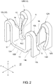
- Fig. 2 is a perspective view showing the connector 10 according to a first embodiment of the invention.
- the connector 10 includes the bottom part 11 which is fixed to the circuit board 2 and a pinching part 12 which pinches the strand 4.
- the pinching part 12 of the connector 10 opens upward.
- the pinching part 12 includes the pair of pinching elements 12L and 12R raised upright from the bottom part 11 and can pinch the strand 4 of the cable 3 in the space S between the pair of pinching elements 12L and 12R.
- the connector 10 includes two sets of pinching parts 12 arranged in the extension direction X of the strand 4 with the bottom part 11 interposed therebetween.
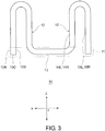
- Fig. 3 is a side view of the connector 10 when viewed from a direction Y orthogonal to the thickness direction Z of the circuit board 2 and the extension direction X of the strand 4.
- the connector 10 is formed by, for example, bending a single metal foil and the bottom part 11 and the pinching part 12 are integrally formed with each other.
- the metal foil constituting the connector 10 includes a first surface 10A, a second surface 10B which is on the side opposite to the first surface 10A, and an end surface 10C which connects the first and second surfaces 10A and 10B.
- the connector 10 is not limited to the bent metal foil and may be formed by plating a block having the bottom part 11 and the pinching part 12 protruding from the bottom part 11 with a conductive material.
- the pinching part 12 includes a pair of first pinching elements 14L and 14R and a pair of second pinching elements 15L and 15R.
- the first pinching elements 14L and 14R are continuous to a bottom plate 13 constituting most of the bottom part 11.
- the second surface 10B of the metal foil is electrically and mechanically connected to the circuit board 2 by fixing through any of soldering, welding, and adhering with a conductive paste.
- the second pinching elements 15L and 15R are continuous to the first pinching elements 14L and 14R.
- the end parts on the side opposite to the first pinching elements 14L and 14R in the second pinching elements 15L and 15R constitute the rest of the bottom part 11.
- the end parts of the second pinching elements 15L and 15R constituting a part of the bottom part 11 are preferably fixed to the circuit board 2, but may not be essentially fixed to the circuit board 2.
- the pinching element 12L (12R) becomes arched and is not easily deformed even when a force pressing the cable 3 into the connector 10 acts.
- the second surface 10B of the metal foils of the first pinching elements 14L and 14R faces the second surface 10B of the metal foils of the second pinching elements 15L and 15R.
- Fig. 4 is a plan view of the connector 10 when viewed from the thickness direction Z of the circuit board 2. As shown in Fig. 4 , all of creases F1 and F4 between the bottom plate 13 and the first pinching elements 14L and 14R and creases F2 and F3 between the first pinching elements 14L and 14R and the second pinching elements 15L and 15R extend in the above-described direction Y. When the metal foil of the connector 10 is unfolded, the metal foil has a substantially rectangular shape and four sides extend in the extension direction X of the strand 4 and the crease direction Y of the metal foil.
- Fig. 5 is a rear view of the connector 10 when viewed from the tip side of the strand 4 in the extension direction X.
- the pair of first pinching elements 14L and 14R is formed mirror-symmetrically when viewed from the intermediate position of the pair of pinching elements 14L and 14R (for example, the center of the pinched strand 4).
- the pair of second pinching elements 15L and 15R is formed mirror-symmetrically when viewed from the intermediate position of the second pinching elements 15L and 15R.
- the pair of first pinching elements 14L and 14R faces each other with an interval D1 interposed therebetween.
- the first pinching elements 14L and 14R are provided with a receiving part 16 which is formed at the end parts on the side opposite to the bottom part 11, that is, the end parts on the side of the second pinching elements 15L and 15R, so that the interval D1 becomes narrow as it goes toward the bottom part 11.
- the end surface 10C of the metal foil is formed in a wedge shape and functions as a pressure-contact blade for cutting the inner covering 7.
- the pair of second pinching elements 15L and 15R faces each other with an interval D2 interposed therebetween.
- the second pinching elements 15L and 15R are provided with a returning part 17 which is formed at the end parts on the side opposite to the bottom part 11, that is, the end parts on the side of the first pinching elements 14L and 14R, so that the interval D2 becomes narrow as it goes away from the bottom part 11.
- the returning part 17 is formed to be narrower than the diameter of the inner covering 7 for covering the core wire 6 in a part where the interval D2 is the narrowest.
- the end parts (hereinafter, referred to as the lower end parts) on the side of the bottom part 11 in the pair of second pinching elements 15L and 15R are not continuous and are independent of each other. Additionally, as in a third embodiment or a fourth embodiment to be described later, the lower end parts of the pair of second pinching elements 15L and 15R may be formed continuously.
- the lower end parts of the pair of second pinching elements 15L and 15R are continuous, the second pinching elements 15L and 15R are not likely to be deformed and the strength of the connector 10 is improved. Since the contact area between the connector 10 and the circuit board 2 is wide, the joint strength between them is improved.
- the pair of second pinching elements 15L and 15R can be widened like a spring. Accordingly, the strand 4 having a large thickness of the inner covering 7 can also be accommodated in a space S2 between those pinching elements. Further, since the circuit board 2 is exposed between the lower end parts of the pair of second pinching elements 15L and 15R, the height of the cable 3 can be suppressed by bringing the strand 4 closer to the circuit board 2.
- the lower end parts of the pair of second pinching elements 15L and 15R are formed so that the interval D2 becomes narrow as it goes toward the bottom part 11. In other words, it is formed so that the hem becomes wider as it goes toward the circuit board 2 so that the contact area is wide when fixed to the circuit board 2.
- Figs. 6A and 6B are perspective views showing a usage example of the connector 10 according to the first embodiment of the invention.
- Fig. 6A when the strand 4 is pressed from above the connector 10 toward the bottom part 11, the strand 4 is guided by the receiving part 16.
- Fig. 6B when the strand 4 is further pressed, the inner covering 7 is cut by the end surface 10C of the receiving part 16 and the core wire 6 is pinched in the space S1 sandwiched by the pair of first pinching elements 14 constituting the pinching part 12.
- the space S1 is an example of the space S inside the pinching part 12.
- the connector 10 is composed of a conductive material such as a metal foil and at least a part (for example, the bottom plate 13) of the bottom part 11 is electrically and mechanically connected to the circuit board 2. Therefore, the strand 4 pinched by the pinching part 12 is electrically and mechanically connected to the circuit board 2 via the connector 10. That is, the strand 4 is mounted on the circuit board 2.
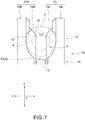
- Fig. 7 is a rear view of the strand 4 mounted on the connector 10 when viewed from the tip side.
- the interval D1 of the pair of first pinching elements 14L and 14R is formed to be narrower than the diameter of the core wire 6 in a part on the side of the bottom part 11 in relation to the receiving part 16. Therefore, the pair of first pinching elements 14L and 14R can bite into the core wire 6 to be conductive to the core wire 6 and to fix the core wire 6 to the circuit board 2.
- the interval D1 is formed to be about 70% of the diameter of the core wire 6.
- At least one of the intervals D1 and D2 of the first pinching elements 14L and 14R and the second pinching elements 15L and 15R is formed to be narrower than the diameter of the core wire 6 in a part on the side of the bottom part 11 in relation to the receiving part 16. Therefore, the connector 10 can fix the strand 4 by the pinching part 12 regardless of the presence of the inner covering 7.
- Fig. 8 is a perspective view showing a usage example of the connector 10 according to a modified example of the first embodiment of the invention.
- the inner covering 7 may be cut so that the core wire 6 is exposed and the core wire 6 exposed from the inner covering 7 may be covered with a solder layer.
- the pair of second pinching elements 15L and 15R faces the core wire 6 with a gap.
- the strand 4 may be moved in the extension direction X so that the inner covering 7 is pinched in the space S2 sandwiched by the pair of second pinching elements 15L and 15R (indicated by a virtual line in Fig. 8 ).
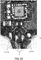
- Fig. 20 is a diagram of a conventional sensor shown for comparison with the invention.
- the strand 4 was directly soldered to the circuit board 2. If the interval between the strands 4 is too narrow, solder may flow to the adjacent strands 4 and cause a short-circuit or the soldering iron may contact with the adjacent strands 4 to cause damage. Further, the quality of soldering and the working time are easily affected by an operator and the appearance, connection reliability, and the like may vary.
- the strand 4 can be mounted at a high density to decrease the size of the sensor 1.
- the connector 10 according to the first embodiment of the invention is formed by a bent metal foil.
- the pair of first pinching elements 14L and 14R pinches the core wire 6 by the end surface 10C. If the strand 4 is pinched by the first surface 10A or the second surface 10B of the bent metal foil, the metal foil is like to be bent when an external force acts. Accordingly, there is concern that the strand 4 cannot be reliably fixed. Meanwhile, according to the first embodiment, since the strand is pinched by the end surface 10C of the metal foil which is less likely to be deformed, the strand 4 can be reliably fixed. Further, the pinching part 12 is provided at a plurality of positions in the extension direction X of the strand 4. Since the strand 4 is pinched at a plurality of positions, the strand 4 can be more reliably fixed.
- the pair of first pinching elements 14L and 14R is formed mirror-symmetrically when viewed from the intermediate position of the first pinching elements 14L and 14R.
- the pair of second pinching elements 15L and 15R is formed mirror-symmetrically when viewed from the intermediate position of the second pinching elements 15L and 15R. Even a minute connector 10 does not undergo overly complicated press working due to the simple shape with symmetry.
- the connector 10 is formed by a metal foil in which all creases F1, F2, F3, and F4 are bent a plurality of times in the direction Y orthogonal to the extension direction X of the strand 4. Since all creases F1, F2, F3, and F4 are parallel to each other, even a minute connector does not undergo overly complicated press working.
- each of the first pinching elements 14L and 14R is provided with the receiving part 16 provided at the tips of the first pinching elements 14L and 14R and provided so that the interval D1 of the pair of first pinching elements 14L and 14R becomes narrow as it goes toward the bottom part 11, the strand 4 can be easily aligned.
- the end surface 10C of the metal foil is formed in a wedge shape. Since the inner covering 7 is cut by the end surface 10C of the receiving part 16 when the strand 4 is pressed into the connector 10, the core wire 6 and the pinching part 12 can be conductive to each other. Therefore, the strand 4 covered with the inner covering 7 can be pressed into the connector 10.
- Each of the second pinching elements 15L and 15R is provided with the returning part 17 in which the interval D2 of the pair of second pinching elements 15L and 15R becomes narrow as it goes away from the bottom part 11.
- the returning part 17 is formed to be narrower than the diameter of the inner covering 7 in a part where the interval D2 is the narrowest. Therefore, it is possible to prevent the strand 4 from coming off from the connector 10 when the inner covering 7 of the strand 4 is disposed to be pinched in the space S2 sandwiched by the pair of second pinching elements 15L and 15R.
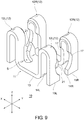
- Fig. 9 is a perspective view showing the connector 10 according to the second embodiment of the invention.
- the connector 10 according to the second embodiment is different from the first embodiment in that a pressure-contact blade 21 raised upright from the bottom part 11 is provided.
- the pressure-contact blade 21 is raised upright from the bottom plate 13.
- Fig. 10 is a rear view in which the connector 10 is viewed from the tip side in the extension direction X of the strand 4. As shown in Fig. 10 , when the circuit board 2 is placed on a horizontal plane, the pressure-contact blade 21 protrudes upward. In the second embodiment, the first pinching elements 14L and 14R are provided with the returning part 17 instead of the receiving part 16.
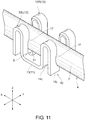
- Fig. 11 is a perspective view showing a usage example of the connector 10 according to the second embodiment of the invention.
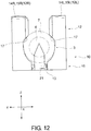
- Fig. 12 is a rear view transparently showing a part of the strand mounted on the connector.
- the inner covering 7 is cut by the pressure-contact blade 21.
- the pressure-contact blade 21 penetrates the inner covering 7 to be conductive to the core wire 6.
- the sensor 1 of the second embodiment since the pressure-contact blade 21 penetrating the inner covering 7 to be conductive to the core wire 6 is provided, the strand 4 covered with the inner covering 7 can be pressed into the connector 10.
- the connector 10 according to the third embodiment will be described with reference to Figs. 13 to 15B .
- the connector 10 according to the third embodiment is different from the first embodiment in that the strand 4 is not fixed in the state shown in Figs. 14A to 15A in which the connector 10 is not tightened and the strand 4 is pinched by the pair of pinching elements 12L and 12R in the state shown in Fig. 15B in which the connector 10 is tightened.
- Fig. 13 is a perspective view showing the connector 10 according to the third embodiment of the invention.
- the interval D1 of the pair of first pinching elements 14L and 14R is formed to be substantially the same from the end part on the side of the bottom part 11 to the end part on the side opposite to the bottom part 11.
- the interval D2 of the pair of second pinching elements 15L and 15R is formed to be substantially the same from the vicinity of the end part on the side of the bottom part 11 to the end part on the side opposite to the bottom part 11.
- the end parts of the pair of second pinching elements 15L and 15R on the side of the bottom part 11 are connected.
- the end surface 10C pinching the strand 4 is formed in a wedge shape and functions as a pressure-contact blade.
- the end surface 10C of the metal foil of the first pinching elements 14L and 14R is formed in a wedge shape.
- Figs. 14A and 14B are perspective views showing a usage example of the connector 10 according to the third embodiment of the invention.
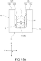
- Fig. 15A is a rear view transparently showing a part of the connector 10 and the strand 4 shown in Fig. 14B .
- Fig. 15B is a diagram showing a state in which the connector 10 shown in Fig. 15A is tightened.
- the interval D1 of the pair of first pinching elements 14L and 14R is formed to be substantially the same as or slightly narrower than the diameter of the core wire 6 in the state in which the connector 10 is not tightened.
- the connector 10 When the strand 4 is fixed to the connector 10, as shown in Fig. 15B , the connector 10 is tightened so that the interval D1 of the first pinching elements 14L and 14R becomes narrow and the core wire 6 is pinched by the pair of first pinching elements 14L and 14R. Additionally, the end surfaces 10C of the second pinching elements 15L and 15R can be formed in a wedge shape and the core wire 6 can be pinched by the pair of second pinching elements 15L and 15R.
- the strand 4 can be freely moved and aligned in the state shown in Figs. 14A to 15A in which the connector 10 is not tightened. Since it is not necessary to press the strand 4 into the connector 10 against the frictional resistance and the restoring force of the pinching part 12, the burden on the operator can be reduced. Since the pair of pinching elements 12L and 12R which is irreversibly deformed bites into the core wire 6 in the state shown in Fig. 15B in which the connector 10 is tightened, the strand 4 is reliably pinched by the connector 10. Since the end surface 10C is formed in a wedge shape, the first pinching elements 14L and 14R penetrate the inner covering 7 to be conductive to the core wire 6. Additionally, the pressure-contact blade formed on the end surface 10C can be omitted when using the strand 4 in which the inner covering 7 at the tip is cut in advance (see Fig. 8 ).
- the connector 10 according to the fourth embodiment will be described with reference to Figs. 16 to 18 .
- the connector 10 according to the fourth embodiment includes pressure-contact blades 41 and 42 which are provided in the pinching elements 12L and 12R.
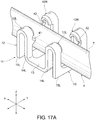
- This embodiment is different from the first embodiment in that the strand 4 is not fixed in the state shown in Fig. 17A in which the connector 10 is not tightened and the strand 4 is fixed in the state shown in Fig. 17B in which the connector 10 is tightened.
- Fig. 16 is a perspective view showing the connector 10 according to the fourth embodiment of the invention.
- the first pinching element 14L is provided with the pressure-contact blade 41 and the second pinching element 15R is provided with the pressure-contact blade 42.
- the pressure-contact blade 41 provided in one first pinching element 14L protrudes toward the other first pinching element 14R.
- the pressure-contact blade 42 provided in the other second pinching element 15R protrudes toward one second pinching element 15L.
- the pressure-contact blade provided in the pinching part 12 may be any one of the pressure-contact blades 41 and 42.
- the pressure-contact blade 41 may be provided in the other first pinching element 14R or may be provided in both first pinching elements 14L and 14R.
- the pressure-contact blade 42 may be provided in one second pinching element 15L or may be provided in both second pinching elements 15L and 15R.
- the receiving part 16 nor the returning part 17 is provided in the connector 10h.
- the interval D1 of the pair of first pinching elements 14L and 14R is formed to be substantially the same in the thickness direction Z of the circuit board 2.
- the interval D2 of the pair of second pinching elements 15L and 15R is formed to be substantially the same in the thickness direction Z of the circuit board 2.
- Figs. 17A and 17B are perspective views showing a usage example of the connector 10 according to the fourth embodiment of the invention.
- the intervals D1 and D2 of the pair of pinching elements 12L and 12R are formed to be substantially the same as the diameter of the inner covering 7 in the state in which the connector 10 is not tightened.
- the connector 10 is tightened so that the intervals D1 and D2 of the pair of pinching elements 12L and 12R become narrow and the strand 4 is pinched by the pinching part 12.
- Fig. 18 is a rear view transparently showing a part of the strand 4 mounted on the connector 10.
- the pressure-contact blades 41 and 42 penetrate the inner covering 7 to be conductive to the core wire 6 in the state in which the connector 10 is tightened.
- the strand 4 is reliably pinched by the connector 10. Since the pressure-contact blade 21 penetrating the inner covering 7 to be conductive to the core wire 6 is provided, there is no need to expose the core wire 6 by cutting the inner covering 7 at the tip of the strand 4 and cover the core wire 6 with the solder layer.
- Fig. 19 is a flowchart showing an example of a procedure of mounting the cable 3 of the invention.
- the connector 10 is composed of a conductive material such as a metal foil in a first step indicated by reference numeral 101.
- a second step indicated by reference numeral 201 an electronic component such as a sensor element and the connector 10 are automatically mounted on the circuit board 2 using a solder printing machine, a component mounting machine, and a reflow furnace.
- a third step indicated by reference numeral 202 the strand 4 is pressed into the connector 10 and the strand 4 is pinched by the pinching part 12.
- the strand 4 is mounted on the circuit board 2 via the connector 10 at this time point.
- the strand 4 is mounted on the circuit board 2 via the connector 10 when the connector 10 is tightened and the strand 4 is completely fixed in a fourth step indicated by reference numeral 203.
- Fig. 21 is a flowchart showing an example of a procedure of mounting the cable 3 of a conventional example.
- an operator manually soldered the strand 4 to the circuit board 2 in a step indicated by reference numeral 204.
- the heavy load step 204 can be replaced with the light load steps 202 and 203.
- the operator manually cut off the inner covering 7 at the tip of the strand 4 using a wire stripper in a step indicated by reference numeral 301.
- a fifth step indicated by reference numeral 302 the operator manually covered the core wire 6 with a solder layer so that the conductive wire would not spread.
- the pressure-contact blade penetrating the inner covering 7 is not a configuration essential for the connector 10 and can be omitted. In that case, for example, the inner covering 7 of the tip of the strand 4 may be cut by the steps 301 and 302.
- a sensor (1) including:
- a method of manufacturing a sensor (1) including:
Landscapes
- Engineering & Computer Science (AREA)
- Manufacturing & Machinery (AREA)
- Coupling Device And Connection With Printed Circuit (AREA)
- Multi-Conductor Connections (AREA)
- Switches That Are Operated By Magnetic Or Electric Fields (AREA)
- Connections By Means Of Piercing Elements, Nuts, Or Screws (AREA)
- Manufacturing Of Electrical Connectors (AREA)
Abstract
Description
- The invention relates to a sensor.
- A strand that transmits signals of electronic components such as sensor elements mounted on a circuit board is connected to the circuit board of the sensor (for example, see Patent Literature 1).
- [Patent Literature 1]
Japanese Patent Laid-Open No. 2018-152266 - As the sensor becomes smaller, the number of components mounted on the circuit board increases, and thus the interval between adjacent strands in the mounting space of the circuit board on which the strands are mounted is narrowed. However, since the strands are mounted on the circuit board by soldering, if the interval between the strands is too narrow, solder may flow to the adjacent strands and cause a short-circuit or a high-temperature soldering iron may contact with the adjacent strands and cause damage. Further, the quality of soldering and the working time are easily affected by an operator and the appearance, connection reliability, and the like may vary.
- As the mounting space for strands increases, it becomes more difficult to solder a cable to the circuit board. Here, an objective of the invention is to provide a sensor capable of easily mounting a cable on a circuit board.
- A sensor according to an aspect of the present disclosure includes: a circuit board; a connector which is composed of a metal material and which is fixed to the circuit board; and a cable which is connected to the circuit board via the connector. The connector includes a bottom part connected to the circuit board and a pair of pinching elements raised upright from the bottom part. The cable is pinched in a space sandwiched between the pair of pinching elements.
- According to this aspect, since soldering can be omitted in the step of mounting the cable on the circuit board, the cable can be easily mounted on the circuit board. In addition, the sensor can be miniaturized by mounting the wires at high density.
Since soldering which tends to vary depending on the operator can be omitted, it is possible to prevent the occurrence of defective products, improve quality, and make them uniform. Since it is possible to assemble even by an unskilled person and shorten the work time, it is possible to decrease a cost. - In the above-described aspect, a plurality of pinching parts including the pair of pinching elements may be provided in an extension direction of the cable.
- According to this aspect, the cable is pinched at a plurality of positions. Accordingly, even when the cable comes off in one of the pinching parts, the cable can be fixed in the other pinching parts. The strength when the cable is pulled is improved and the cable can be fixed more reliably.
- In the above-described aspect, the pair of pinching elements may be formed mirror-symmetrically when viewed from an intermediate position of the pair of pinching elements.
- According to this aspect, even a minute connector does not undergo overly complicated press working due to the simple shape with symmetry. The manufacturability in the step of forming the connector is excellent.
- In the above-described aspect, the connector may be formed by a bent metal foil. The metal foil includes a first surface, a second surface on the side opposite to the first surface, and an end surface connecting the first surface and the second surface. The pair of pinching elements may pinch the cable by using the end surface.
- If the cable is pinched by the first surface or the second surface of the bent metal foil, the metal foil is likely to be bent when an external force is applied. Accordingly, there is concern that the cable cannot be reliably fixed. According to this aspect, since the cable is pinched by the end surface of the metal foil which is not likely to be deformed, the cable can be reliably fixed.
- In the above-described aspect, the connector may be formed by the metal foil bent a plurality of times so that all creases are orthogonal to the extension direction of the cable.
- According to this aspect, since all creases are parallel to each other, even a minute connector does not undergo overly complicated press working. The manufacturability in the step of forming the connector is excellent.
- In the above-described aspect, the second surface in the bottom part may be connected to the circuit board. The pinching element may include a pair of first pinching elements pinching the cable and a pair of second pinching elements disposed along the first pinching elements. The second surface of the first pinching element may face the second surface of the second pinching element.
- According to this aspect, since the cable is pinched at a plurality of positions by the first pinching element and the second pinching element, the strength when the cable is pulled is improved and the cable can be fixed more reliably. The first pinching element and the second pinching element can be configured to pinch other members of the cable. For example, the first pinching element may be configured to pinch the core wire of the cable and the second pinching element may be configured to pinch the inner covering of the cable.
- In the above-described aspect, the cable may include a plurality of strands and an outer covering bundling the plurality of strands and each of the strands may include a core wire composed of a plurality of conductive wires and an inner covering covering the core wire. The pair of first pinching elements may pinch the core wire.
- According to this aspect, the cable can be mounted on the circuit board just by pressing the cable toward the bottom part. The core wire may be covered with the inner covering or may be exposed from the inner covering.
- In the above-described aspect, the first pinching element may include a receiving part provided at a tip of the first pinching element and provided so that an interval of the pair of first pinching elements becomes narrow as it goes toward the bottom part.
- According to this aspect, the cable can be easily aligned by being guided to the receiving part.
- In the above-described aspect, the end surfaces of the pair of pinching elements in the receiving part may be formed in a wedge shape.
- According to this aspect, the connector and the core wire can be electrically connected to each other by cutting the inner covering with the pressure-contact blade formed on the end surface of the receiving part.
- In the above-described aspect, the cable may include a plurality of strands and an outer covering bundling the plurality of strands and each of the strands may include a core wire composed of a plurality of conductive wires and an inner covering covering the core wire. All of the pair of first pinching elements and the pair of second pinching elements may pinch the inner covering. At least one of the bottom part, the first pinching element, and the second pinching element may include a pressure-contact blade that penetrates the inner covering and is conductive to the core wire.
- According to this aspect, since it is possible to omit the step of exposing the core wire by cutting the inner covering, the manufacturability in the step of mounting the cable on the circuit board is excellent. Since the pressure-contact blade bites into the cable, the cable does not easily come off.
- In the above-described aspect, the pinching element may include a returning part provided so that an interval of the pair of pinching elements becomes narrow as it goes away from the bottom part. The returning part may be formed to be narrower than a diameter of the inner covering in a portion in which the interval of the pair of pinching elements is the narrowest.
- According to this aspect, since the returning part is provided, it is possible to prevent the cable from coming off from the connector.
- In the above-described aspect, each of the first pinching element and the second pinching element may include the pressure-contact blade. A plurality of the pressure-contact blades may penetrate the inner covering while the connector is tightened so that the interval of the pair of first pinching elements becomes narrow and the interval of the pair of second pinching elements becomes narrow.
- According to this aspect, since it is possible to omit the step of exposing the core wire by cutting the inner covering, the manufacturability in the step of mounting the cable on the circuit board is excellent. Since the pressure-contact blade is conductive to the core wire at a plurality of positions, the connection reliability of finished products is improved. Since the connector is tightened and irreversibly deformed and the pressure-contact blade bites into the cable, the cable does not easily come off.
- In the above-described aspect, the cable may not be fixed while the connector is not tightened and the cable may be pinched by the pair of pinching elements while the connector is tightened so that the interval of the pair of pinching elements becomes narrow.
- According to this aspect, since the cable is not fixed until the cable is tightened, the distance of the pair of pinching elements can be increased. The cable can be easily placed between the pair of pinching elements. When the connector is tightened, the connector is irreversibly deformed and the cable does not easily come off.
- A sensor manufacturing method according to an aspect of the present disclosure includes: a first step of forming a connector including a bottom part and a pair of pinching elements raised upright from the bottom part by a metal material; a second step of connecting the connector to a circuit board; and a third step of pressing a cable toward the bottom part and pinching the cable in a space sandwiched between the pair of pinching elements.
- According to this aspect, since soldering can be omitted in the step of mounting the cable on the circuit board, the cable can be easily mounted on the circuit board.
- In the above-described aspect, the connector may be connected to the circuit board by fixing through any of soldering, welding, and adhering with a conductive paste.
- According to this aspect, the pre-manufactured connector can be easily mounted on the circuit board.
- The cable may include a plurality of strands and an outer covering bundling the plurality of strands and each of the strands may include a core wire composed of a plurality of conductive wires and an inner covering covering the core wire. The connector may further include a pressure-contact blade provided in the bottom part. In the third step, the pressure-contact blade may penetrate the inner covering to be conductive to the core wire.
- According to this aspect, since it is possible to omit the step of exposing the core wire by cutting the inner covering, the manufacturability in the step of mounting the cable on the circuit board is excellent. Since the pressure-contact blade bites into the cable, the cable does not easily come off.
- In the above-described aspect, the connector may further include a pressure-contact blade provided in the pinching element. The sensor manufacturing method may further include, after the third step, a fourth step of tightening the connector so that an interval of the pair of pinching elements becomes narrow. In the fourth step, the pressure-contact blade may penetrate the inner covering to be conductive to the core wire.
- According to this aspect, since it is possible to omit the step of exposing the core wire by cutting the inner covering, the manufacturability in the step of mounting the cable on the circuit board is excellent. Since the connector is tightened and irreversibly deformed and the pressure-contact blade bites into the cable, the cable does not easily come off.
- In the above-described aspect, the sensor manufacturing method may further include a fifth step of covering the core wire with a solder layer. The sensor manufacturing method may further include, after the third step, a fourth step of tightening the connector so that the interval of the pair of pinching elements becomes narrow. In the fourth step, the pinching element may penetrate the solder layer to be conductive to the core wire.
- According to this aspect, since the pinching element is directly conductive to the core wire, the connection reliability of finished products is improved. Since the connector is tightened and irreversibly deformed, the cable does not easily come off.
- According to the invention, it is possible to provide a sensor capable of easily mounting a cable on a circuit board.
-
-
Fig. 1 is a diagram showing an internal structure of a sensor according to an embodiment of the invention. -
Fig. 2 is a perspective view showing a connector according to a first embodiment of the invention. -
Fig. 3 is a side view of the connector shown inFig. 2 . -
Fig. 4 is a plan view of the connector shown inFig. 2 . -
Fig. 5 is a rear view of the connector shown inFig. 2 . -
Fig. 6A is a perspective view showing a usage example of the connector according to the first embodiment of the invention. -
Fig. 6B is a perspective view showing a usage example of the connector according to the first embodiment of the invention afterFig. 6A . -
Fig. 7 is a rear view of a strand mounted on the connector as viewed from a tip side. -
Fig. 8 is a perspective view showing a modified example of the connector shown inFig. 6B . -
Fig. 9 is a perspective view showing a connector according to a second embodiment of the invention. -
Fig. 10 is a rear view of the connector shown inFig. 9 . -
Fig. 11 is a perspective view showing a usage example of the connector according to the second embodiment of the invention. -
Fig. 12 is a rear view transparently showing a part of a strand mounted on the connector. -
Fig. 13 is a perspective view showing a connector according to a third embodiment of the invention. -
Fig. 14A is a perspective view showing a usage example of the connector according to the third embodiment of the invention. -
Fig. 14B is a perspective view showing a usage example of the connector according to the third embodiment of the invention afterFig. 14A . -
Fig. 15A is a rear view transparently showing a part of the connector and the strand shown inFig. 14B . -
Fig. 15B is a rear view showing a usage example of the connector according to the third embodiment of the invention afterFig. 15A . -
Fig. 16 is a perspective view showing a connector according to a fourth embodiment of the invention. -
Fig. 17A is a perspective view showing a usage example of the connector according to the fourth embodiment of the invention. -
Fig. 17B is a perspective view showing a usage example of the connector according to the fourth embodiment of the invention afterFig. 17A . -
Fig. 18 is a rear view transparently showing a part of the strand mounted on the connector. -
Fig. 19 is a flowchart showing an example of a procedure of mounting the strand in the invention. -
Fig. 20 is a diagram of a conventional sensor shown for comparison with the invention. -
Fig. 21 is a flowchart showing an example of a procedure of mounting the strand in the conventional example shown inFig. 20 . - Preferred embodiments of the invention will be described with reference to the accompanying drawings. In the drawings, those having the same reference numerals have the same or similar configurations. A
sensor 1 of an embodiment of the invention includes aconnector 10 which is composed of a conductive material such as a metal foil (seeFig. 1 ). Theconnector 10 includes abottom part 11 and a pair of pinchingelements Figs. 2 ,9 ,13 , and16 ). Since it is only necessary to press astrand 4 into a space S between the pair of pinchingelements Fig. 6A ), acable 3 can be easily mounted on a circuit board 2 (seeFig. 7 ). Acore wire 6 of thestrand 4 may be covered with an inner covering 7 (seeFig. 6B ) or may be exposed from the inner covering 7 (seeFig. 8 ). Theconnector 10 may be tightened in order to more strongly fix the strand 4 (seeFigs. 15B and18 ). Hereinafter, each configuration will be described in detail with reference toFigs. 1 to 21 . - First, a configuration common to each embodiment will be described with reference to
Fig. 1. Fig. 1 is a perspective view showing thesensor 1 of an embodiment of the invention. As shown inFig. 1 , thesensor 1 includes acircuit board 2 on which an electronic component such as a sensor element is mounted, a plurality ofconnectors 10 which are mounted on thecircuit board 2, and acable 3 which is connected to thecircuit board 2 via theconnector 10 and transmits a signal from a sensor element. Thecable 3 includes thestrand 4 which is electrically and mechanically connected to eachconnector 10 and anouter covering 5 which bundles the plurality ofstrands 4. Thestrand 4 includes thecore wire 6 composed of a plurality of conductive wires and theinner covering 7 covering thecore wire 6. -
Fig. 2 is a perspective view showing theconnector 10 according to a first embodiment of the invention. As shown inFig. 2 , theconnector 10 includes thebottom part 11 which is fixed to thecircuit board 2 and a pinchingpart 12 which pinches thestrand 4. When thecircuit board 2 is placed on a horizontal plane, the pinchingpart 12 of theconnector 10 opens upward. The pinchingpart 12 includes the pair of pinchingelements bottom part 11 and can pinch thestrand 4 of thecable 3 in the space S between the pair of pinchingelements connector 10 includes two sets of pinchingparts 12 arranged in the extension direction X of thestrand 4 with thebottom part 11 interposed therebetween. -
Fig. 3 is a side view of theconnector 10 when viewed from a direction Y orthogonal to the thickness direction Z of thecircuit board 2 and the extension direction X of thestrand 4. As shown inFig. 3 , theconnector 10 is formed by, for example, bending a single metal foil and thebottom part 11 and the pinchingpart 12 are integrally formed with each other. The metal foil constituting theconnector 10 includes afirst surface 10A, asecond surface 10B which is on the side opposite to thefirst surface 10A, and anend surface 10C which connects the first andsecond surfaces connector 10 is not limited to the bent metal foil and may be formed by plating a block having thebottom part 11 and the pinchingpart 12 protruding from thebottom part 11 with a conductive material. - The pinching
part 12 includes a pair offirst pinching elements second pinching elements first pinching elements bottom plate 13 constituting most of thebottom part 11. In thebottom plate 13, thesecond surface 10B of the metal foil is electrically and mechanically connected to thecircuit board 2 by fixing through any of soldering, welding, and adhering with a conductive paste. - The
second pinching elements first pinching elements first pinching elements second pinching elements bottom part 11. The end parts of thesecond pinching elements bottom part 11 are preferably fixed to thecircuit board 2, but may not be essentially fixed to thecircuit board 2. When the end part of thesecond pinching element 15L (15R) is fixed to thecircuit board 2, the pinchingelement 12L (12R) becomes arched and is not easily deformed even when a force pressing thecable 3 into theconnector 10 acts. Thesecond surface 10B of the metal foils of thefirst pinching elements second surface 10B of the metal foils of thesecond pinching elements -
Fig. 4 is a plan view of theconnector 10 when viewed from the thickness direction Z of thecircuit board 2. As shown inFig. 4 , all of creases F1 and F4 between thebottom plate 13 and thefirst pinching elements first pinching elements second pinching elements connector 10 is unfolded, the metal foil has a substantially rectangular shape and four sides extend in the extension direction X of thestrand 4 and the crease direction Y of the metal foil. -
Fig. 5 is a rear view of theconnector 10 when viewed from the tip side of thestrand 4 in the extension direction X. In the example shown inFig. 5 , the pair offirst pinching elements elements second pinching elements second pinching elements Fig. 5 , the pair offirst pinching elements first pinching elements part 16 which is formed at the end parts on the side opposite to thebottom part 11, that is, the end parts on the side of thesecond pinching elements bottom part 11. In the receivingpart 16, theend surface 10C of the metal foil is formed in a wedge shape and functions as a pressure-contact blade for cutting theinner covering 7. - Similarly to the pair of
first pinching elements second pinching elements second pinching elements part 17 which is formed at the end parts on the side opposite to thebottom part 11, that is, the end parts on the side of thefirst pinching elements bottom part 11. The returningpart 17 is formed to be narrower than the diameter of theinner covering 7 for covering thecore wire 6 in a part where the interval D2 is the narrowest. - In the example shown in the drawings, the end parts (hereinafter, referred to as the lower end parts) on the side of the
bottom part 11 in the pair ofsecond pinching elements second pinching elements second pinching elements second pinching elements connector 10 is improved. Since the contact area between theconnector 10 and thecircuit board 2 is wide, the joint strength between them is improved. - Meanwhile, when the lower end parts of the pair of
second pinching elements second pinching elements strand 4 having a large thickness of theinner covering 7 can also be accommodated in a space S2 between those pinching elements. Further, since thecircuit board 2 is exposed between the lower end parts of the pair ofsecond pinching elements cable 3 can be suppressed by bringing thestrand 4 closer to thecircuit board 2. - In the example shown in the drawings, the lower end parts of the pair of
second pinching elements bottom part 11. In other words, it is formed so that the hem becomes wider as it goes toward thecircuit board 2 so that the contact area is wide when fixed to thecircuit board 2. -
Figs. 6A and6B are perspective views showing a usage example of theconnector 10 according to the first embodiment of the invention. As shown inFig. 6A , when thestrand 4 is pressed from above theconnector 10 toward thebottom part 11, thestrand 4 is guided by the receivingpart 16. As shown inFig. 6B , when thestrand 4 is further pressed, theinner covering 7 is cut by theend surface 10C of the receivingpart 16 and thecore wire 6 is pinched in the space S1 sandwiched by the pair of first pinching elements 14 constituting the pinchingpart 12. The space S1 is an example of the space S inside the pinchingpart 12. Theconnector 10 is composed of a conductive material such as a metal foil and at least a part (for example, the bottom plate 13) of thebottom part 11 is electrically and mechanically connected to thecircuit board 2. Therefore, thestrand 4 pinched by the pinchingpart 12 is electrically and mechanically connected to thecircuit board 2 via theconnector 10. That is, thestrand 4 is mounted on thecircuit board 2. -
Fig. 7 is a rear view of thestrand 4 mounted on theconnector 10 when viewed from the tip side. As shown inFig. 7 , the interval D1 of the pair offirst pinching elements core wire 6 in a part on the side of thebottom part 11 in relation to the receivingpart 16. Therefore, the pair offirst pinching elements core wire 6 to be conductive to thecore wire 6 and to fix thecore wire 6 to thecircuit board 2. In the example shown in the drawings, the interval D1 is formed to be about 70% of the diameter of thecore wire 6. - At least one of the intervals D1 and D2 of the
first pinching elements second pinching elements core wire 6 in a part on the side of thebottom part 11 in relation to the receivingpart 16. Therefore, theconnector 10 can fix thestrand 4 by the pinchingpart 12 regardless of the presence of theinner covering 7. -
Fig. 8 is a perspective view showing a usage example of theconnector 10 according to a modified example of the first embodiment of the invention. As shown inFig. 8 , in thestrand 4, theinner covering 7 may be cut so that thecore wire 6 is exposed and thecore wire 6 exposed from theinner covering 7 may be covered with a solder layer. In the example shown in the drawings, the pair ofsecond pinching elements core wire 6 with a gap. Additionally, thestrand 4 may be moved in the extension direction X so that theinner covering 7 is pinched in the space S2 sandwiched by the pair ofsecond pinching elements Fig. 8 ). - Since the
sensor 1 of the first embodiment of the invention with the above-described configuration can omit soldering in the step of mounting thestrand 4 of thecable 3 on thecircuit board 2, thecable 3 can be easily mounted on thecircuit board 2.Fig. 20 is a diagram of a conventional sensor shown for comparison with the invention. In the conventional sensor, thestrand 4 was directly soldered to thecircuit board 2. If the interval between thestrands 4 is too narrow, solder may flow to theadjacent strands 4 and cause a short-circuit or the soldering iron may contact with theadjacent strands 4 to cause damage. Further, the quality of soldering and the working time are easily affected by an operator and the appearance, connection reliability, and the like may vary. - In contrast, in the
sensor 1 of the first embodiment of the invention, since soldering which tends to vary depending on the operator can be omitted, it is possible to prevent the occurrence of defective products, improve quality, and make them uniform. Since it is possible to assemble even by an unskilled person and shorten the work time, it is possible to decrease a cost. Since it is not necessary to partition a mounting space as large as soldering on thecircuit board 2, thestrand 4 can be mounted at a high density to decrease the size of thesensor 1. - The
connector 10 according to the first embodiment of the invention is formed by a bent metal foil. The pair offirst pinching elements core wire 6 by theend surface 10C. If thestrand 4 is pinched by thefirst surface 10A or thesecond surface 10B of the bent metal foil, the metal foil is like to be bent when an external force acts. Accordingly, there is concern that thestrand 4 cannot be reliably fixed. Meanwhile, according to the first embodiment, since the strand is pinched by theend surface 10C of the metal foil which is less likely to be deformed, thestrand 4 can be reliably fixed. Further, the pinchingpart 12 is provided at a plurality of positions in the extension direction X of thestrand 4. Since thestrand 4 is pinched at a plurality of positions, thestrand 4 can be more reliably fixed. - In the
connector 10 according to the first embodiment of the invention, the pair offirst pinching elements first pinching elements second pinching elements second pinching elements minute connector 10 does not undergo overly complicated press working due to the simple shape with symmetry. In addition, theconnector 10 is formed by a metal foil in which all creases F1, F2, F3, and F4 are bent a plurality of times in the direction Y orthogonal to the extension direction X of thestrand 4. Since all creases F1, F2, F3, and F4 are parallel to each other, even a minute connector does not undergo overly complicated press working. - Since each of the
first pinching elements part 16 provided at the tips of thefirst pinching elements first pinching elements bottom part 11, thestrand 4 can be easily aligned. In the receivingpart 16, theend surface 10C of the metal foil is formed in a wedge shape. Since theinner covering 7 is cut by theend surface 10C of the receivingpart 16 when thestrand 4 is pressed into theconnector 10, thecore wire 6 and the pinchingpart 12 can be conductive to each other. Therefore, thestrand 4 covered with theinner covering 7 can be pressed into theconnector 10. - Each of the
second pinching elements part 17 in which the interval D2 of the pair ofsecond pinching elements bottom part 11. The returningpart 17 is formed to be narrower than the diameter of theinner covering 7 in a part where the interval D2 is the narrowest. Therefore, it is possible to prevent thestrand 4 from coming off from theconnector 10 when theinner covering 7 of thestrand 4 is disposed to be pinched in the space S2 sandwiched by the pair ofsecond pinching elements - Next, the
connectors 10 according to second to fourth embodiments of the invention will be described. For the configuration having the same or similar function as the configuration described in the first embodiment, the description of the corresponding first embodiment will be referred to with the same reference numerals and the description thereof will be omitted here. Further, the configurations other than those described below are the same as those of the first embodiment. - The
connector 10 according to the second embodiment will be described with reference toFigs. 9 to 12 .Fig. 9 is a perspective view showing theconnector 10 according to the second embodiment of the invention. As shown inFig. 9 , theconnector 10 according to the second embodiment is different from the first embodiment in that a pressure-contact blade 21 raised upright from thebottom part 11 is provided. In the example shown in the drawings, the pressure-contact blade 21 is raised upright from thebottom plate 13. -
Fig. 10 is a rear view in which theconnector 10 is viewed from the tip side in the extension direction X of thestrand 4. As shown inFig. 10 , when thecircuit board 2 is placed on a horizontal plane, the pressure-contact blade 21 protrudes upward. In the second embodiment, thefirst pinching elements part 17 instead of the receivingpart 16.Fig. 11 is a perspective view showing a usage example of theconnector 10 according to the second embodiment of the invention. -
Fig. 12 is a rear view transparently showing a part of the strand mounted on the connector. As shown inFig. 12 , when thestrand 4 is pressed into theconnector 10, theinner covering 7 is cut by the pressure-contact blade 21. In the state in which thestrand 4 is mounted on theconnector 10, the pressure-contact blade 21 penetrates theinner covering 7 to be conductive to thecore wire 6. According to thesensor 1 of the second embodiment, since the pressure-contact blade 21 penetrating theinner covering 7 to be conductive to thecore wire 6 is provided, thestrand 4 covered with theinner covering 7 can be pressed into theconnector 10. - The
connector 10 according to the third embodiment will be described with reference toFigs. 13 to 15B . Theconnector 10 according to the third embodiment is different from the first embodiment in that thestrand 4 is not fixed in the state shown inFigs. 14A to 15A in which theconnector 10 is not tightened and thestrand 4 is pinched by the pair of pinchingelements Fig. 15B in which theconnector 10 is tightened. -
Fig. 13 is a perspective view showing theconnector 10 according to the third embodiment of the invention. As shown inFig. 13 , in the third embodiment, neither the receivingpart 16 nor the returningpart 17 is provided on theconnector 10. The interval D1 of the pair offirst pinching elements bottom part 11 to the end part on the side opposite to thebottom part 11. Similarly, the interval D2 of the pair ofsecond pinching elements bottom part 11 to the end part on the side opposite to thebottom part 11. In the example shown in the drawings, the end parts of the pair ofsecond pinching elements bottom part 11 are connected. - In one or both of the first and
second pinching elements end surface 10C pinching thestrand 4 is formed in a wedge shape and functions as a pressure-contact blade. In the example shown in the drawings, theend surface 10C of the metal foil of thefirst pinching elements Figs. 14A and14B are perspective views showing a usage example of theconnector 10 according to the third embodiment of the invention.Fig. 15A is a rear view transparently showing a part of theconnector 10 and thestrand 4 shown inFig. 14B .Fig. 15B is a diagram showing a state in which theconnector 10 shown inFig. 15A is tightened. As shown inFigs. 13A to 15A , the interval D1 of the pair offirst pinching elements core wire 6 in the state in which theconnector 10 is not tightened. - When the
strand 4 is fixed to theconnector 10, as shown inFig. 15B , theconnector 10 is tightened so that the interval D1 of thefirst pinching elements core wire 6 is pinched by the pair offirst pinching elements second pinching elements core wire 6 can be pinched by the pair ofsecond pinching elements - According to the
sensor 1 of the third embodiment, thestrand 4 can be freely moved and aligned in the state shown inFigs. 14A to 15A in which theconnector 10 is not tightened. Since it is not necessary to press thestrand 4 into theconnector 10 against the frictional resistance and the restoring force of the pinchingpart 12, the burden on the operator can be reduced. Since the pair of pinchingelements core wire 6 in the state shown inFig. 15B in which theconnector 10 is tightened, thestrand 4 is reliably pinched by theconnector 10. Since theend surface 10C is formed in a wedge shape, thefirst pinching elements inner covering 7 to be conductive to thecore wire 6. Additionally, the pressure-contact blade formed on theend surface 10C can be omitted when using thestrand 4 in which theinner covering 7 at the tip is cut in advance (seeFig. 8 ). - The
connector 10 according to the fourth embodiment will be described with reference toFigs. 16 to 18 . Theconnector 10 according to the fourth embodiment includes pressure-contact blades pinching elements strand 4 is not fixed in the state shown inFig. 17A in which theconnector 10 is not tightened and thestrand 4 is fixed in the state shown inFig. 17B in which theconnector 10 is tightened. -
Fig. 16 is a perspective view showing theconnector 10 according to the fourth embodiment of the invention. In the example shown in the drawings, thefirst pinching element 14L is provided with the pressure-contact blade 41 and thesecond pinching element 15R is provided with the pressure-contact blade 42. The pressure-contact blade 41 provided in onefirst pinching element 14L protrudes toward the otherfirst pinching element 14R. Similarly, the pressure-contact blade 42 provided in the othersecond pinching element 15R protrudes toward onesecond pinching element 15L. - Additionally, the pressure-contact blade provided in the pinching
part 12 may be any one of the pressure-contact blades contact blade 41 may be provided in the otherfirst pinching element 14R or may be provided in bothfirst pinching elements contact blade 42 may be provided in onesecond pinching element 15L or may be provided in bothsecond pinching elements - As shown in
Fig. 16 , in the fourth embodiment, neither the receivingpart 16 nor the returningpart 17 is provided in the connector 10h. The interval D1 of the pair offirst pinching elements circuit board 2. Similarly, the interval D2 of the pair ofsecond pinching elements circuit board 2. -
Figs. 17A and17B are perspective views showing a usage example of theconnector 10 according to the fourth embodiment of the invention. As shown inFig. 17A , the intervals D1 and D2 of the pair of pinchingelements inner covering 7 in the state in which theconnector 10 is not tightened. When thestrand 4 is fixed to theconnector 10, as shown inFig. 17B , theconnector 10 is tightened so that the intervals D1 and D2 of the pair of pinchingelements strand 4 is pinched by the pinchingpart 12. -
Fig. 18 is a rear view transparently showing a part of thestrand 4 mounted on theconnector 10. As shown inFig. 18 , the pressure-contact blades inner covering 7 to be conductive to thecore wire 6 in the state in which theconnector 10 is tightened. According to thesensor 1 of the fourth embodiment, since the pressure-contact blades elements strand 4, thestrand 4 is reliably pinched by theconnector 10. Since the pressure-contact blade 21 penetrating theinner covering 7 to be conductive to thecore wire 6 is provided, there is no need to expose thecore wire 6 by cutting theinner covering 7 at the tip of thestrand 4 and cover thecore wire 6 with the solder layer. - Next, a method of manufacturing the
sensor 1 of the invention will be described.Fig. 19 is a flowchart showing an example of a procedure of mounting thecable 3 of the invention. In the method of manufacturing thesensor 1 of the invention, theconnector 10 is composed of a conductive material such as a metal foil in a first step indicated byreference numeral 101. In a second step indicated byreference numeral 201, an electronic component such as a sensor element and theconnector 10 are automatically mounted on thecircuit board 2 using a solder printing machine, a component mounting machine, and a reflow furnace. - In a third step indicated by
reference numeral 202, thestrand 4 is pressed into theconnector 10 and thestrand 4 is pinched by the pinchingpart 12. In the case of thesensor 1 of the first and second embodiments, thestrand 4 is mounted on thecircuit board 2 via theconnector 10 at this time point. In the case of thesensor 1 of the third and fourth embodiments, thestrand 4 is mounted on thecircuit board 2 via theconnector 10 when theconnector 10 is tightened and thestrand 4 is completely fixed in a fourth step indicated byreference numeral 203. -
Fig. 21 is a flowchart showing an example of a procedure of mounting thecable 3 of a conventional example. In the conventional sensor manufacturing method, an operator manually soldered thestrand 4 to thecircuit board 2 in a step indicated byreference numeral 204. As described so far, in theultra-small sensor 1, it is a heavy burden on the operator to solder thestrand 4 to the narrow mounting space of thecircuit board 2. According to the method of manufacturing thesensor 1 of the invention, theheavy load step 204 can be replaced with the light load steps 202 and 203. - Further, in the conventional sensor manufacturing method, the operator manually cut off the
inner covering 7 at the tip of thestrand 4 using a wire stripper in a step indicated byreference numeral 301. In a fifth step indicated byreference numeral 302, the operator manually covered thecore wire 6 with a solder layer so that the conductive wire would not spread. According to the method of manufacturing thesensor 1 of the invention, such a manual step can also be omitted. Additionally, the pressure-contact blade penetrating theinner covering 7 is not a configuration essential for theconnector 10 and can be omitted. In that case, for example, theinner covering 7 of the tip of thestrand 4 may be cut by thesteps - The embodiments described above are for facilitating the understanding of the invention and are not for limiting the interpretation of the invention. Each element included in the embodiment and its arrangement, material, condition, shape, size, and the like are not limited to those exemplified and can be changed as appropriate. In addition, the configurations shown in different embodiments can be partially replaced or combined.
- A sensor (1) including:
- a circuit board;
- a connector (10) which is composed of a metal material and is fixed to the circuit board (2); and
- a cable (3) which is connected to the circuit board (2) via the connector (10),
- wherein the connector (10) includes a bottom part (11) connected to the circuit board (2) and a pair of pinching elements (12L, 12R) raised upright from the bottom part (11), and
- wherein the cable (3) is pinched in a space (S) sandwiched by the pair of pinching elements (12L, 12R).
- A method of manufacturing a sensor (1) including:
- a first step (101) of forming a connector (10) including a bottom part (11) and a pair of pinching elements (12L, 12R) raised upright from the bottom part (11) using a metal material;
- a second step (201) of connecting the connector (10) to a circuit board (2); and
- a third step (202) of pressing a cable (3) toward the bottom part (11) and holding the cable (3) in a space (S) between the pair of pinching elements (12L, 12R).
-
- 1 Electronic device
- 2 Circuit board
- 3 Cable
- 4 Strand
- 5 Outer covering
- 6 Core wire
- 7 Inner covering
- 10 Connector
- 10A First surface
- 10B Second surface
- 10C End surface
- 11 Bottom part
- 12 Pinching part
- 12L, 12R Pinching element
- 13 Bottom plate
- 14L, 14R First pinching element
- 15L, 15R Second pinching element
- 16 Receiving part
- 17 Returning part
- 21, 41, 42 Pressure-contact blade
- 101 First step
- 201 Second step
- 202 Third step
- 203 Fourth step
- 301, 302 Other steps
- D1, D2 Interval
- F1, F2, F3, F4 Crease
- S, S1, S2 Space
- X Extension direction of strand
- Y Direction parallel to crease
- Z Thickness direction of circuit board
Claims (16)
- A sensor comprising:a circuit board;a connector which is composed of a metal material and which is fixed to the circuit board; anda cable which is connected to the circuit board via the connector,wherein the connector includes a bottom part connected to the circuit board and a pair of pinching elements raised upright from the bottom part, andwherein the cable is pinched in a space sandwiched by the pair of pinching elements.
- The sensor according to claim 1,
wherein a plurality of pinching parts including the pair of pinching elements are provided in an extension direction of the cable. - The sensor according to claim 1 or 2,
wherein the pair of pinching elements is formed mirror-symmetrically when viewed from an intermediate position of the pair of pinching elements. - The sensor according to any one of claims 1 to 3,wherein the connector is formed by a bent metal foil,wherein the metal foil includes a first surface, a second surface on a side opposite to the first surface, and an end surface connecting the first surface and the second surface, andwherein the pair of pinching elements pinches the cable by using the end surface.
- The sensor according to claim 4,
wherein the connector is formed of the metal foil bent a plurality of times so that all creases are orthogonal to an extension direction of the cable. - The sensor according to claim 5,wherein in the bottom part, the second surface is connected to the circuit board,wherein the pair of pinching elements includes a pair of first pinching elements pinching the cable and a pair of second pinching elements disposed along the first pinching elements, andwherein the second surface of the first pinching element faces the second surface of the second pinching element.
- The sensor according to claim 6,wherein the cable includes a plurality of strands and an outer covering bundling the plurality of strands,wherein each of the strands includes a core wire composed of a plurality of conductive wires and an inner covering covering the core wire,wherein the pair of first pinching elements pinches the core wire, andwherein the pair of second pinching elements pinches the inner covering.
- The sensor according to claim 7,
wherein the first pinching element includes a receiving part provided at a tip of the first pinching element and provided so that an interval of the pair of first pinching elements becomes narrow as it goes toward the bottom part. - The sensor according to claim 8,
wherein the end surface of the first pinching element in the receiving part is formed in a wedge shape. - The sensor according to claim 6,wherein the cable includes a plurality of strands and an outer covering bundling the plurality of strands,wherein each of the strands includes a core wire composed of a plurality of conductive wires and an inner covering covering the core wire,wherein all of the pair of first pinching elements and the pair of second pinching elements pinch the inner covering, andwherein at least one of the bottom part, the first pinching element, and the second pinching element includes a pressure-contact blade that penetrates the inner covering and is conductive to the core wire.
- The sensor according to claim 10,wherein the pinching element further includes a returning part provided so that an interval of the pair of pinching elements becomes narrow as it goes away from the bottom part, andwherein the returning part is formed to be narrower than a diameter of the inner covering in a portion in which the interval of the pair of pinching elements is the narrowest.
- The sensor according to claim 10,wherein each of the first pinching element and the second pinching element includes the pressure-contact blade, andwherein a plurality of pressure-contact blades penetrate the inner covering while the connector is tightened so that the interval of the pair of first pinching elements becomes narrow and the interval of the pair of second pinching elements becomes narrow.
- A sensor manufacturing method comprising:a first step of forming a connector including a bottom part and a pair of pinching elements raised upright from the bottom part by a metal material;a second step of connecting the connector to a circuit board; anda third step of pressing a cable toward the bottom part and pinching the cable in a space sandwiched between the pair of pinching elements.
- The sensor manufacturing method according to claim 13,
wherein the connector is connected to the circuit board by fixing through any of soldering, welding, and adhering with a conductive paste. - The sensor manufacturing method according to claim 13 or 14,wherein the cable includes a plurality of strands and an outer covering bundling the plurality of strands,wherein each of the strands includes a core wire composed of a plurality of conductive wires and an inner covering covering the core wire,wherein the connector further includes a pressure-contact blade provided in the bottom part, andwherein in the third step, the pressure-contact blade penetrates the inner covering to be conductive to the core wire.
- The sensor manufacturing method according to claim 13 or 14,wherein the cable includes a plurality of strands and an outer covering bundling the plurality of strands,wherein each of the strands includes a core wire composed of a plurality of conductive wires and an inner covering covering the core wire,wherein the connector further includes a pressure-contact blade provided in the pinching element,wherein the sensor manufacturing method may further comprise, after the third step, a fourth step of tightening the connector so that an interval of the pair of pinching elements becomes narrow, andwherein in the fourth step, the pressure-contact blade penetrates the inner covering to be conductive to the core wire.
Applications Claiming Priority (2)
| Application Number | Priority Date | Filing Date | Title |
|---|---|---|---|
| JP2018225792A JP7044043B2 (en) | 2018-11-30 | 2018-11-30 | Sensor |
| PCT/JP2019/041592 WO2020110526A1 (en) | 2018-11-30 | 2019-10-24 | Sensor |
Publications (3)
| Publication Number | Publication Date |
|---|---|
| EP3890117A1 true EP3890117A1 (en) | 2021-10-06 |
| EP3890117A4 EP3890117A4 (en) | 2022-08-03 |
| EP3890117B1 EP3890117B1 (en) | 2026-01-07 |
Family
ID=70852126
Family Applications (1)
| Application Number | Title | Priority Date | Filing Date |
|---|---|---|---|
| EP19889362.0A Active EP3890117B1 (en) | 2018-11-30 | 2019-10-24 | Sensor |
Country Status (6)
| Country | Link |
|---|---|
| US (1) | US11831119B2 (en) |
| EP (1) | EP3890117B1 (en) |
| JP (1) | JP7044043B2 (en) |
| KR (1) | KR102573368B1 (en) |
| CN (1) | CN112655116B (en) |
| WO (1) | WO2020110526A1 (en) |
Families Citing this family (4)
| Publication number | Priority date | Publication date | Assignee | Title |
|---|---|---|---|---|
| CN102931252B (en) * | 2012-10-22 | 2015-06-17 | 苏州中来光伏新材股份有限公司 | Solar cell module support member and machining process thereof |
| JP2022040491A (en) * | 2020-08-31 | 2022-03-11 | 矢崎総業株式会社 | Pressure welding structure, and electric wire with terminal and manufacturing method thereof |
| JP7408592B2 (en) | 2021-03-23 | 2024-01-05 | 矢崎総業株式会社 | wire with terminal |
| KR102516073B1 (en) * | 2021-06-04 | 2023-03-31 | 주식회사 남전사 | Smart meter using non-contact current control measuring IC and fixing support |
Family Cites Families (15)
| Publication number | Priority date | Publication date | Assignee | Title |
|---|---|---|---|---|
| US3854114A (en) * | 1972-08-10 | 1974-12-10 | J Kloth | Notched plate clasp apparatus |
| US3937549A (en) * | 1974-06-18 | 1976-02-10 | Amp Incorporated | Strimp |
| JPS5322085U (en) * | 1976-08-05 | 1978-02-24 | ||
| US4370009A (en) * | 1980-07-25 | 1983-01-25 | Amp Incorporated | Slotted plate terminal renewable as spade terminal |
| US4363529A (en) * | 1980-07-25 | 1982-12-14 | Amp Incorporated | Terminal having improved mounting means |
| US4350404A (en) * | 1980-09-24 | 1982-09-21 | Bell Telephone Laboratories, Incorporated | Electrical connector construction |
| JPH08329995A (en) * | 1995-05-31 | 1996-12-13 | Sumitomo Wiring Syst Ltd | Pressure contact terminal |
| US6722007B2 (en) * | 2002-01-24 | 2004-04-20 | Chia Hsien Lin | Electric cord connector kit |
| FR2852744B1 (en) * | 2003-03-21 | 2006-12-22 | Cotterlaz Jean Sas | SELF-CONTAINING CONNECTOR FOR CIRCUIT COMPONENTS MOUNTED ON SURFACE. |
| JP2011029125A (en) * | 2009-07-29 | 2011-02-10 | Sumitomo Wiring Syst Ltd | Insulation displacement connector |
| CN110890639B (en) * | 2013-04-18 | 2021-07-06 | 安费诺富加宜(亚洲)私人有限公司 | Insulation displacement connector and contact thereof |
| CN105431980B (en) * | 2013-07-30 | 2020-06-30 | 安费诺富加宜(亚洲)私人有限公司 | Insulation displacement connector |
| EP3266069B1 (en) * | 2015-03-03 | 2021-12-29 | Amphenol FCI Asia Pte Ltd | Insulation displacement connector |
| JP6852479B2 (en) | 2017-03-14 | 2021-03-31 | オムロン株式会社 | Proximity sensor |
| KR101905678B1 (en) * | 2018-05-03 | 2018-10-11 | 주식회사 소암컨설턴트 | DTHi sensor module and thereby fire prevention monitoring system |
-
2018
- 2018-11-30 JP JP2018225792A patent/JP7044043B2/en active Active
-
2019
- 2019-10-24 CN CN201980058179.7A patent/CN112655116B/en active Active
- 2019-10-24 US US17/287,114 patent/US11831119B2/en active Active
- 2019-10-24 EP EP19889362.0A patent/EP3890117B1/en active Active
- 2019-10-24 KR KR1020217008695A patent/KR102573368B1/en active Active
- 2019-10-24 WO PCT/JP2019/041592 patent/WO2020110526A1/en not_active Ceased
Also Published As
| Publication number | Publication date |
|---|---|
| US20210359430A1 (en) | 2021-11-18 |
| US11831119B2 (en) | 2023-11-28 |
| CN112655116B (en) | 2022-12-27 |
| EP3890117B1 (en) | 2026-01-07 |
| JP7044043B2 (en) | 2022-03-30 |
| KR102573368B1 (en) | 2023-09-01 |
| CN112655116A (en) | 2021-04-13 |
| KR20210043693A (en) | 2021-04-21 |
| WO2020110526A1 (en) | 2020-06-04 |
| EP3890117A4 (en) | 2022-08-03 |
| JP2020087885A (en) | 2020-06-04 |
Similar Documents
| Publication | Publication Date | Title |
|---|---|---|
| US11831119B2 (en) | Sensor and sensor manufacturing method | |
| US9444159B2 (en) | Terminal for contacting an electrical conductor | |
| JP4036378B2 (en) | connector | |
| JP5258923B2 (en) | Cable fixture | |
| JP4652742B2 (en) | connector | |
| JPS6217824B2 (en) | ||
| TWI547044B (en) | Method of connecting a cable with a cable connector | |
| JP5376639B2 (en) | Crimp terminal structure and harness | |
| US10862254B2 (en) | Coated conductive wire connecting method, coated conductive wire connecting structure and coated conductive wire connecting member | |
| JP2009037748A (en) | Cable connector and cable connection method | |
| JP5622051B2 (en) | Board terminal and board connector using the same | |
| JP6908927B2 (en) | Terminal | |
| JP3272147B2 (en) | Cross wiring method and cross wiring structure of flat cable and flat cable having the cross wiring structure | |
| CN104347992A (en) | Crimp connector, crimp connector with wires and connection method between the crimp and coated wires | |
| US3932017A (en) | Electrical terminal assembly and terminal therefor | |
| JP4807796B2 (en) | Cable connector and cable connection method | |
| CN100511858C (en) | Connector | |
| HU220727B1 (en) | Connecting arrangement, his process for making and electric apparatus having said arrangement | |
| CN210779032U (en) | Electrode plate contact pin | |
| JP2014063612A (en) | Connector | |
| CN111740235B (en) | Connector for conductive cloth | |
| JP6282818B2 (en) | Pressure contact connector and wire pressure contact connector | |
| JP6097633B2 (en) | connector | |
| JP2013038008A (en) | Method of pressure welding electric wire, and pressure welding connector | |
| JP2001035555A (en) | Contact for connecting coaxial cable |
Legal Events
| Date | Code | Title | Description |
|---|---|---|---|
| STAA | Information on the status of an ep patent application or granted ep patent |
Free format text: STATUS: THE INTERNATIONAL PUBLICATION HAS BEEN MADE |
|
| PUAI | Public reference made under article 153(3) epc to a published international application that has entered the european phase |
Free format text: ORIGINAL CODE: 0009012 |
|
| STAA | Information on the status of an ep patent application or granted ep patent |
Free format text: STATUS: REQUEST FOR EXAMINATION WAS MADE |
|
| 17P | Request for examination filed |
Effective date: 20210413 |
|
| AK | Designated contracting states |
Kind code of ref document: A1 Designated state(s): AL AT BE BG CH CY CZ DE DK EE ES FI FR GB GR HR HU IE IS IT LI LT LU LV MC MK MT NL NO PL PT RO RS SE SI SK SM TR |
|
| DAV | Request for validation of the european patent (deleted) | ||
| DAX | Request for extension of the european patent (deleted) | ||
| A4 | Supplementary search report drawn up and despatched |
Effective date: 20220701 |
|
| RIC1 | Information provided on ipc code assigned before grant |
Ipc: H01R 4/2466 20180101ALI20220627BHEP Ipc: H01R 12/53 20110101ALI20220627BHEP Ipc: H01R 12/57 20110101ALI20220627BHEP Ipc: H01R 4/2462 20180101ALI20220627BHEP Ipc: H01R 43/01 20060101ALI20220627BHEP Ipc: H01R 12/51 20110101ALI20220627BHEP Ipc: H01R 4/26 20060101ALI20220627BHEP Ipc: H01R 4/2495 20180101ALI20220627BHEP Ipc: H01R 4/2455 20180101ALI20220627BHEP Ipc: H01R 4/2406 20180101ALI20220627BHEP Ipc: H01R 4/2454 20180101AFI20220627BHEP |
|
| STAA | Information on the status of an ep patent application or granted ep patent |
Free format text: STATUS: EXAMINATION IS IN PROGRESS |
|
| 17Q | First examination report despatched |
Effective date: 20240612 |
|
| 17Q | First examination report despatched |
Effective date: 20240625 |
|
| GRAP | Despatch of communication of intention to grant a patent |
Free format text: ORIGINAL CODE: EPIDOSNIGR1 |
|
| STAA | Information on the status of an ep patent application or granted ep patent |
Free format text: STATUS: GRANT OF PATENT IS INTENDED |
|
| INTG | Intention to grant announced |
Effective date: 20251021 |
|
| GRAS | Grant fee paid |
Free format text: ORIGINAL CODE: EPIDOSNIGR3 |
|
| GRAA | (expected) grant |
Free format text: ORIGINAL CODE: 0009210 |
|
| STAA | Information on the status of an ep patent application or granted ep patent |
Free format text: STATUS: THE PATENT HAS BEEN GRANTED |
|
| AK | Designated contracting states |
Kind code of ref document: B1 Designated state(s): AL AT BE BG CH CY CZ DE DK EE ES FI FR GB GR HR HU IE IS IT LI LT LU LV MC MK MT NL NO PL PT RO RS SE SI SK SM TR |
|
| REG | Reference to a national code |
Ref country code: CH Ref legal event code: F10 Free format text: ST27 STATUS EVENT CODE: U-0-0-F10-F00 (AS PROVIDED BY THE NATIONAL OFFICE) Effective date: 20260107 Ref country code: GB Ref legal event code: FG4D |
|
| REG | Reference to a national code |
Ref country code: DE Ref legal event code: R096 Ref document number: 602019080235 Country of ref document: DE |
|
| REG | Reference to a national code |
Ref country code: IE Ref legal event code: FG4D |
|
| REG | Reference to a national code |
Ref country code: NL Ref legal event code: MP Effective date: 20260107 |
|
| PG25 | Lapsed in a contracting state [announced via postgrant information from national office to epo] |
Ref country code: NL Free format text: LAPSE BECAUSE OF FAILURE TO SUBMIT A TRANSLATION OF THE DESCRIPTION OR TO PAY THE FEE WITHIN THE PRESCRIBED TIME-LIMIT Effective date: 20260107 |
|
| REG | Reference to a national code |
Ref country code: AT Ref legal event code: MK05 Ref document number: 1876241 Country of ref document: AT Kind code of ref document: T Effective date: 20260107 |
|
| PG25 | Lapsed in a contracting state [announced via postgrant information from national office to epo] |
Ref country code: RS Free format text: LAPSE BECAUSE OF FAILURE TO SUBMIT A TRANSLATION OF THE DESCRIPTION OR TO PAY THE FEE WITHIN THE PRESCRIBED TIME-LIMIT Effective date: 20260407 |
|
| PG25 | Lapsed in a contracting state [announced via postgrant information from national office to epo] |
Ref country code: ES Free format text: LAPSE BECAUSE OF FAILURE TO SUBMIT A TRANSLATION OF THE DESCRIPTION OR TO PAY THE FEE WITHIN THE PRESCRIBED TIME-LIMIT Effective date: 20260107 |
|
| PG25 | Lapsed in a contracting state [announced via postgrant information from national office to epo] |
Ref country code: PL Free format text: LAPSE BECAUSE OF FAILURE TO SUBMIT A TRANSLATION OF THE DESCRIPTION OR TO PAY THE FEE WITHIN THE PRESCRIBED TIME-LIMIT Effective date: 20260107 |
|
| PG25 | Lapsed in a contracting state [announced via postgrant information from national office to epo] |
Ref country code: GR Free format text: LAPSE BECAUSE OF FAILURE TO SUBMIT A TRANSLATION OF THE DESCRIPTION OR TO PAY THE FEE WITHIN THE PRESCRIBED TIME-LIMIT Effective date: 20260408 |
|
| REG | Reference to a national code |
Ref country code: LT Ref legal event code: MG9D |
|
| PG25 | Lapsed in a contracting state [announced via postgrant information from national office to epo] |
Ref country code: LT Free format text: LAPSE BECAUSE OF FAILURE TO SUBMIT A TRANSLATION OF THE DESCRIPTION OR TO PAY THE FEE WITHIN THE PRESCRIBED TIME-LIMIT Effective date: 20260107 |
|
| PG25 | Lapsed in a contracting state [announced via postgrant information from national office to epo] |
Ref country code: NO Free format text: LAPSE BECAUSE OF FAILURE TO SUBMIT A TRANSLATION OF THE DESCRIPTION OR TO PAY THE FEE WITHIN THE PRESCRIBED TIME-LIMIT Effective date: 20260407 |
|
| PG25 | Lapsed in a contracting state [announced via postgrant information from national office to epo] |
Ref country code: FI Free format text: LAPSE BECAUSE OF FAILURE TO SUBMIT A TRANSLATION OF THE DESCRIPTION OR TO PAY THE FEE WITHIN THE PRESCRIBED TIME-LIMIT Effective date: 20260107 Ref country code: AT Free format text: LAPSE BECAUSE OF FAILURE TO SUBMIT A TRANSLATION OF THE DESCRIPTION OR TO PAY THE FEE WITHIN THE PRESCRIBED TIME-LIMIT Effective date: 20260107 Ref country code: SE Free format text: LAPSE BECAUSE OF FAILURE TO SUBMIT A TRANSLATION OF THE DESCRIPTION OR TO PAY THE FEE WITHIN THE PRESCRIBED TIME-LIMIT Effective date: 20260107 |
|
| PG25 | Lapsed in a contracting state [announced via postgrant information from national office to epo] |
Ref country code: HR Free format text: LAPSE BECAUSE OF FAILURE TO SUBMIT A TRANSLATION OF THE DESCRIPTION OR TO PAY THE FEE WITHIN THE PRESCRIBED TIME-LIMIT Effective date: 20260107 |
|
| PG25 | Lapsed in a contracting state [announced via postgrant information from national office to epo] |
Ref country code: IS Free format text: LAPSE BECAUSE OF FAILURE TO SUBMIT A TRANSLATION OF THE DESCRIPTION OR TO PAY THE FEE WITHIN THE PRESCRIBED TIME-LIMIT Effective date: 20260507 Ref country code: PT Free format text: LAPSE BECAUSE OF FAILURE TO SUBMIT A TRANSLATION OF THE DESCRIPTION OR TO PAY THE FEE WITHIN THE PRESCRIBED TIME-LIMIT Effective date: 20260507 |
|
| PG25 | Lapsed in a contracting state [announced via postgrant information from national office to epo] |
Ref country code: LV Free format text: LAPSE BECAUSE OF FAILURE TO SUBMIT A TRANSLATION OF THE DESCRIPTION OR TO PAY THE FEE WITHIN THE PRESCRIBED TIME-LIMIT Effective date: 20260107 |
|
| PG25 | Lapsed in a contracting state [announced via postgrant information from national office to epo] |
Ref country code: BG Free format text: LAPSE BECAUSE OF FAILURE TO SUBMIT A TRANSLATION OF THE DESCRIPTION OR TO PAY THE FEE WITHIN THE PRESCRIBED TIME-LIMIT Effective date: 20260107 |