EP3889679A1 - Optical switch - Google Patents
Optical switch Download PDFInfo
- Publication number
- EP3889679A1 EP3889679A1 EP19888928.9A EP19888928A EP3889679A1 EP 3889679 A1 EP3889679 A1 EP 3889679A1 EP 19888928 A EP19888928 A EP 19888928A EP 3889679 A1 EP3889679 A1 EP 3889679A1
- Authority
- EP
- European Patent Office
- Prior art keywords
- waveguide
- section
- end side
- optical switch
- sections
- Prior art date
- Legal status (The legal status is an assumption and is not a legal conclusion. Google has not performed a legal analysis and makes no representation as to the accuracy of the status listed.)
- Pending
Links
- 230000003287 optical effect Effects 0.000 title claims abstract description 76
- 239000012782 phase change material Substances 0.000 claims abstract description 63
- 230000000644 propagated effect Effects 0.000 claims description 6
- 230000020169 heat generation Effects 0.000 claims description 2
- 239000000463 material Substances 0.000 abstract description 14
- 239000000758 substrate Substances 0.000 description 17
- 230000008878 coupling Effects 0.000 description 12
- 238000010168 coupling process Methods 0.000 description 12
- 238000005859 coupling reaction Methods 0.000 description 12
- 230000001902 propagating effect Effects 0.000 description 7
- 238000003780 insertion Methods 0.000 description 5
- 230000037431 insertion Effects 0.000 description 5
- 238000010586 diagram Methods 0.000 description 4
- 238000004519 manufacturing process Methods 0.000 description 4
- XUIMIQQOPSSXEZ-UHFFFAOYSA-N Silicon Chemical compound [Si] XUIMIQQOPSSXEZ-UHFFFAOYSA-N 0.000 description 3
- 150000004770 chalcogenides Chemical class 0.000 description 3
- 229910052710 silicon Inorganic materials 0.000 description 3
- 239000010703 silicon Substances 0.000 description 3
- 238000012986 modification Methods 0.000 description 2
- 230000004048 modification Effects 0.000 description 2
- 238000012546 transfer Methods 0.000 description 2
- 229910017000 As2Se3 Inorganic materials 0.000 description 1
- JBRZTFJDHDCESZ-UHFFFAOYSA-N AsGa Chemical compound [As]#[Ga] JBRZTFJDHDCESZ-UHFFFAOYSA-N 0.000 description 1
- GYHNNYVSQQEPJS-UHFFFAOYSA-N Gallium Chemical compound [Ga] GYHNNYVSQQEPJS-UHFFFAOYSA-N 0.000 description 1
- 229910001218 Gallium arsenide Inorganic materials 0.000 description 1
- VYPSYNLAJGMNEJ-UHFFFAOYSA-N Silicium dioxide Chemical compound O=[Si]=O VYPSYNLAJGMNEJ-UHFFFAOYSA-N 0.000 description 1
- 229910021417 amorphous silicon Inorganic materials 0.000 description 1
- 229910052787 antimony Inorganic materials 0.000 description 1
- WATWJIUSRGPENY-UHFFFAOYSA-N antimony atom Chemical compound [Sb] WATWJIUSRGPENY-UHFFFAOYSA-N 0.000 description 1
- 239000004020 conductor Substances 0.000 description 1
- 239000013078 crystal Substances 0.000 description 1
- 239000003989 dielectric material Substances 0.000 description 1
- ZZEMEJKDTZOXOI-UHFFFAOYSA-N digallium;selenium(2-) Chemical compound [Ga+3].[Ga+3].[Se-2].[Se-2].[Se-2] ZZEMEJKDTZOXOI-UHFFFAOYSA-N 0.000 description 1
- 230000000694 effects Effects 0.000 description 1
- 229910052733 gallium Inorganic materials 0.000 description 1
- 229910052732 germanium Inorganic materials 0.000 description 1
- GNPVGFCGXDBREM-UHFFFAOYSA-N germanium atom Chemical compound [Ge] GNPVGFCGXDBREM-UHFFFAOYSA-N 0.000 description 1
- 239000011521 glass Substances 0.000 description 1
- AKUCEXGLFUSJCD-UHFFFAOYSA-N indium(3+);selenium(2-) Chemical compound [Se-2].[Se-2].[Se-2].[In+3].[In+3] AKUCEXGLFUSJCD-UHFFFAOYSA-N 0.000 description 1
- 229910052751 metal Inorganic materials 0.000 description 1
- 239000002184 metal Substances 0.000 description 1
- 229910052958 orpiment Inorganic materials 0.000 description 1
- 239000011347 resin Substances 0.000 description 1
- 229920005989 resin Polymers 0.000 description 1
- 239000004065 semiconductor Substances 0.000 description 1
Images


Classifications
-
- G—PHYSICS
- G02—OPTICS
- G02F—OPTICAL DEVICES OR ARRANGEMENTS FOR THE CONTROL OF LIGHT BY MODIFICATION OF THE OPTICAL PROPERTIES OF THE MEDIA OF THE ELEMENTS INVOLVED THEREIN; NON-LINEAR OPTICS; FREQUENCY-CHANGING OF LIGHT; OPTICAL LOGIC ELEMENTS; OPTICAL ANALOGUE/DIGITAL CONVERTERS
- G02F1/00—Devices or arrangements for the control of the intensity, colour, phase, polarisation or direction of light arriving from an independent light source, e.g. switching, gating or modulating; Non-linear optics
- G02F1/29—Devices or arrangements for the control of the intensity, colour, phase, polarisation or direction of light arriving from an independent light source, e.g. switching, gating or modulating; Non-linear optics for the control of the position or the direction of light beams, i.e. deflection
- G02F1/31—Digital deflection, i.e. optical switching
- G02F1/313—Digital deflection, i.e. optical switching in an optical waveguide structure
- G02F1/3132—Digital deflection, i.e. optical switching in an optical waveguide structure of directional coupler type
-
- G—PHYSICS
- G02—OPTICS
- G02B—OPTICAL ELEMENTS, SYSTEMS OR APPARATUS
- G02B6/00—Light guides; Structural details of arrangements comprising light guides and other optical elements, e.g. couplings
- G02B6/24—Coupling light guides
- G02B6/26—Optical coupling means
- G02B6/35—Optical coupling means having switching means
- G02B6/354—Switching arrangements, i.e. number of input/output ports and interconnection types
- G02B6/3544—2D constellations, i.e. with switching elements and switched beams located in a plane
- G02B6/3546—NxM switch, i.e. a regular array of switches elements of matrix type constellation
-
- G—PHYSICS
- G02—OPTICS
- G02B—OPTICAL ELEMENTS, SYSTEMS OR APPARATUS
- G02B6/00—Light guides; Structural details of arrangements comprising light guides and other optical elements, e.g. couplings
- G02B6/24—Coupling light guides
- G02B6/26—Optical coupling means
- G02B6/35—Optical coupling means having switching means
- G02B6/3502—Optical coupling means having switching means involving direct waveguide displacement, e.g. cantilever type waveguide displacement involving waveguide bending, or displacing an interposed waveguide between stationary waveguides
-
- G—PHYSICS
- G02—OPTICS
- G02F—OPTICAL DEVICES OR ARRANGEMENTS FOR THE CONTROL OF LIGHT BY MODIFICATION OF THE OPTICAL PROPERTIES OF THE MEDIA OF THE ELEMENTS INVOLVED THEREIN; NON-LINEAR OPTICS; FREQUENCY-CHANGING OF LIGHT; OPTICAL LOGIC ELEMENTS; OPTICAL ANALOGUE/DIGITAL CONVERTERS
- G02F1/00—Devices or arrangements for the control of the intensity, colour, phase, polarisation or direction of light arriving from an independent light source, e.g. switching, gating or modulating; Non-linear optics
- G02F1/01—Devices or arrangements for the control of the intensity, colour, phase, polarisation or direction of light arriving from an independent light source, e.g. switching, gating or modulating; Non-linear optics for the control of the intensity, phase, polarisation or colour
- G02F1/0147—Devices or arrangements for the control of the intensity, colour, phase, polarisation or direction of light arriving from an independent light source, e.g. switching, gating or modulating; Non-linear optics for the control of the intensity, phase, polarisation or colour based on thermo-optic effects
Definitions
- the present disclosure relates to an optical switch.
- PLT 1 discloses an optical switch whose size can be miniaturized by using a phase change material provided along the core.
- An optical switch according to the first aspect comprises,
- an optical switch 10 is configured to include a first waveguide 11, a second waveguide 12, and an exchanger 13.
- the first waveguide 11, the second waveguide 12, and the exchanger 13 are provided on, for example, a substrate 14. At least, the first waveguide 11 and the second waveguide 12 may be located on the same plane on the substrate 14.
- the substrate 14 may be made of, for example, a conductor such as metal, a semiconductor such as silicon, glass, or resin. In the present embodiment, any two directions perpendicular to each other on the substrate 14 are defined as x-direction and y-direction.
- the first waveguide 11 includes, for example, a first end section 15, a second end section 16, and a first linear section 17.
- the first linear section 17 is a linear section extending in the y-direction.
- the first linear section 17 connects to the first end section 15 at the opposite side end in the y-direction.
- the first linear section 17 is connected to the second end section 16 at the end in the y-direction side.
- the end of the first end section 15 on the opposite side in the y-direction is the first end E1, which is one end of the entire first waveguide 11.
- the end of the second end section 16 on the y-direction side is the second end E2, which is the other end of the entire first waveguide 11.
- the first end E1 and the second end E2 are ports where electromagnetic waves are input and output.
- the second waveguide 12 includes, for example, a third end section 18, a fourth end section 19, and a second linear section 20.
- the second linear section 20 is a linear section extending in the y-direction.
- the second linear section 20 connects to the third end section 18 at the opposite side end in the y-direction.
- the second linear section 20 is connected to the fourth end section 19 at the end on the y-direction side.
- the end of the third end section 18 on the opposite side in the y-direction is the third end E3, which is one end of the entire second waveguide 12.
- the end of the fourth end section 19 on the y-direction side is the fourth end E4, which is one end of the entire second waveguide 12.
- the third end E3 is located on the first end E1 side viewed from the center in the longitudinal direction of the first waveguide 11. Further, the fourth end E4 is located at the second end E2 side viewed from the center in the longitudinal direction of the first waveguide 11.
- the third end E3 and the fourth end E4 are ports where electromagnetic waves are input and output.
- the exchanger 13 comprises at least one first waveguide section 21 and at least one second waveguide section 22.
- the first waveguide section 21 is located along the first waveguide 11.
- the first waveguide section 21 configures a 2 ⁇ 2 directional coupler together with the first waveguide 11.
- the first waveguide section 21 comprises a first phase change material 23.
- the first waveguide section 21 may include a linear section extending in the y-direction.
- the second waveguide section 22 is located along the second waveguide 12.
- the second waveguide section 22 configures a 2 ⁇ 2 directional coupler together with the second waveguide 12.
- the second waveguide section 22 includes a second phase change material 24.
- the second waveguide section 22 may include a linear section extending in the y-direction.
- the first waveguide 11, the second waveguide 12, the first waveguide section 21, and the second waveguide section 22 are composed of a core and a clad.
- the cores of the first waveguide 11, the second waveguide 12, the first waveguide section 21, and the second waveguide section 22 may be made of the same dielectric material to propagate electromagnetic waves such as silicon.
- the clad may be made of a dielectric with a smaller refractive index than the core, such as quartz glass.
- the length of the opposing part may be the coupling length in the state where the first phase change material 23 is changed to the amorphous phase.
- the coupling length is the length from the starting point of the opposing part to the position where the coupling coefficient reaches its maximum value.
- the coupling coefficient is a parameter indicating the ratio of electromagnetic waves to be transferred from one waveguide to the other in a parallel waveguide in which two linear waveguides are lined up. In a configuration where no electromagnetic waves are transferred at all from one waveguide to the other, the coupling coefficient is zero. In a configuration where all electromagnetic waves are transferred from one waveguide to the other, the coupling coefficient is 1.
- the coupling coefficient is included in the range between 0 and 1.
- the coupling coefficient is determined based on the shape of each waveguide, the distance between each waveguide, or the length of the waveguides opposing to each other.
- At least a part of the second linear section 20 are opposing to at least a part of the linear section of the second waveguide section 22.
- the length of the opposing part may be the coupling length in the state where the second phase change material 24 is changed to the amorphous phase.
- the first phase change material 23 and the second phase change material 24 may be displaced from that same plane in a direction perpendicular to the same plane in which the first waveguide 11 and the second waveguide 12 are located.
- the first phase change material 23 and the second phase change material 24 may each be located on the opposite side of the first waveguide section 21 and the second waveguide section 22 from the substrate 14 in a direction perpendicular to the main surface of the substrate 14, that is, the widest surface of the substrate 14.
- the first phase change material 23 and the second phase change material 24 can be phase-changed to an amorphous or a crystalline phase.
- the first phase change material 23 and the second phase change material 24 may be phase-changed by laser beam emitted from a laser source or by heat generation by a resistive element.
- the first phase change material 23 When the first phase change material 23 is an amorphous phase, loss of electromagnetic waves in the first waveguide section 21 is relatively small. Therefore, in this case, because the effective refractive indices of the first linear section 17 and the first waveguide section 21 are substantially the same and the length is also the coupling length, electromagnetic waves input from the first end E1 side of the first linear section 17 and the first waveguide section 21 are respectively output from the second end E2 side of the first waveguide section 21 and the first linear section 17. Similarly, when the second phase change material 24 is an amorphous phase, electromagnetic waves input from the third end E3 side of the second linear section 20 and the second waveguide section 22 are respectively output from the fourth end E4 side of the second waveguide section 22 and the second linear section 20.
- the loss of electromagnetic waves in the first waveguide section 21 is relatively large. Therefore, in this case, because the effective refractive indices of the first linear section 17 and the first waveguide section 21 are significantly different, the electromagnetic waves input from the first end E1 side of the first linear section 17 are not transferred to the first waveguide section 21, in other words, the electromagnetic waves are output from the second end E2 side of the first linear section 17 without propagating through the lossy first waveguide section 21.
- the second phase change material 24 is a crystalline phase, electromagnetic waves input from the third end E3 side of the second linear section 20 are not transferred to the second waveguide section 22, but are output from the fourth end E4 side of the second linear section 20.
- first phase change material 23 and the second phase change material 24 for example, tetrahedral materials such as amorphous silicon, amorphous germanium, amorphous gallium antimony, amorphous gallium arsenide, amorphous indium selenide, amorphous gallium selenide, Ge-Sb-Te chalcogenide materials such as Ge 2 Sb 2 Te 5 and Ge 6 Sb 2 Te 9 , Sb-Te chalcogenide materials, or chalcogenide materials such as As 2 Se 3 , As 2 S 3 , are used.
- tetrahedral materials such as amorphous silicon, amorphous germanium, amorphous gallium antimony, amorphous gallium arsenide, amorphous indium selenide, amorphous gallium selenide, Ge-Sb-Te chalcogenide materials such as Ge 2 Sb 2 Te 5 and Ge 6 Sb 2 Te 9 , Sb-Te chalcogenide materials
- the exchanger 13 inputs electromagnetic waves, input from the first end E1 of the first waveguide 11 and output from any of the first waveguide sections 21 through a directional coupler, to the third end E3 side of any of the second waveguide sections 22.
- the exchanger 13 inputs electromagnetic waves, input from the third end E3 of the second waveguide 12 and output from any of the second waveguide sections 22 through a directional coupler, to the first end E1 side of any of the first waveguide sections 21.
- the first waveguide 11, the second waveguide 12, and the exchanger 13 may satisfy the waveguiding condition in single mode. Therefore, electromagnetic waves, input to at least one of the first end E1 and the third end E3, may be propagated in single mode.
- the exchanger 13 comprises an annular third waveguide 25 and an annular fourth waveguide 26.
- the third waveguide 25 and the fourth waveguide 26 are located, for example, between the first waveguide 11 and the second waveguide 12.
- the third waveguide 25 and the fourth waveguide 26 are arranged to line up along the x-direction, for example.
- the third waveguide 25 is annular including the first waveguide section 21 as a part.
- the third waveguide 25 has a linear first section 27 extending in the y-direction on the opposite side of the first waveguide section 21 in the x-direction.
- the fourth waveguide 26 is annular including the second waveguide section 22 as a part.
- the fourth waveguide 26 has a linear second section 28 extending in the y-direction on the opposite side of the second waveguide section 22 in the x-direction.
- the second section 28, that is a part of the fourth waveguide 26, is opposing to the first section 27, that is a part of the third waveguide 25, and configures a 2 ⁇ 2 directional coupler.
- the length of the first section 27 and the second section 28 is the coupling length. Therefore, the electromagnetic waves, respectively input to the first section 27 and the second section 28, can be output from the second section 28 and the first section 27 at a higher intensity than the other sections.
- the optical switch 10 of the first embodiment comprises: at least one first waveguide section 21 configuring a directional coupler together with the first waveguide 11 and including a first phase change material 23; at least one second waveguide section 22 configuring a directional coupler together with a second waveguide 12 and including a second phase change material 24; and an exchanger 13, configured to: input electromagnetic waves, input from the first end E1 and output from any of the first waveguide sections 21, to the third end E3 side of any of the second waveguide sections 22; and to input electromagnetic waves, input from the third end E3 and output from any of the second waveguide sections 22, to the second end E2 side of any of the first waveguide sections 21.
- the optical switch 10 can cause electromagnetic waves, input to the first end E1 and the third end E3, to respectively output from the second end E2 and the fourth end E4 without causing them to propagate through the first waveguide section 21 and
- the optical switch 10 can cause electromagnetic waves, input to the first end E1 and the third end E3, to propagate through the first waveguide section 21 and the second waveguide section 22 in a state where the loss is relatively small, and to respectively output from the fourth end E4 and the second end E2. Therefore, in the crystal phases of the first phase change material 23 and the second phase change material 24 that relatively increase loss of electromagnetic waves in the first waveguide section 21 and the second waveguide section 22, the optical switch 10 can switch the output destination of the electromagnetic waves without causing the electromagnetic waves to propagate through the first waveguide section 21 and the second waveguide section 22. Therefore, the optical switch 10 can reduce insertion loss while using the first phase change material 23 and the second phase change material 24.
- electromagnetic waves input to at least one of the first end E1 and the third end E3, are propagated in single mode.
- the optical switch 10 can be suitably used for optical communications because the waveform of the propagating signal is less likely to be collapsed.
- the first waveguide 11 and the second waveguide 12 are located on the same plane.
- the optical switch 10 can be easily produced on the substrate 14 as compared to the configuration in which both are displaced in the direction perpendicular to the main surface.
- the first phase change material 23 and the second phase change material 24 are displaced from the same plane, in which the first waveguide 11 and the second waveguide 12 are located, in a direction perpendicular to the same plane.
- the optical switch 10 can form the first phase change material 23 and the second phase change material 24 in separate layers after forming the waveguides configurating the first waveguide 11, the second waveguide 12, and the exchanger 13.
- the waveguides configuring the first waveguide 11, the second waveguide 12, and the exchanger 13 can be made of the same material but different from the first phase change material 23 and second phase change material 24. Therefore, the optical switch 10, configured as described above, can be easily produced by such a production method that layers are formed for each of the same materials.
- the optical switch according to the second embodiment of the present disclosure will be described.
- the configuration of the exchanger is different from that in the first embodiment.
- the second embodiment will be described below, focusing on the different points from the first embodiment. It is noted that the same reference signs are given to the parts with the same configuration as that in the first embodiment.
- the optical switch 100 is similar to that of the first embodiment and is configured to include a first waveguide 11, a second waveguide 12, and an exchanger 130.
- the configuration and function of the first waveguide 11 and the second waveguide 12 are the same as those in the first embodiment.
- the exchanger 130 comprises at least one first waveguide section 21 and at least one second waveguide section 22, as in the first embodiment.
- the configuration and function of the first waveguide section 21 and the second waveguide section 22 are the same as those in the first embodiment.
- the exchanger 130 inputs electromagnetic waves, input from the first end E1 of the first waveguide 11 and output from any of the first waveguide sections 21 through a directional coupler, to the third end E3 side of any of the second waveguide sections 22.
- the exchanger 130 inputs electromagnetic waves, input from the third end E3 of the second waveguide 12 and output from any of the second waveguide sections 22 through a directional coupler, to the first end E1 side of any of the first waveguide sections 21.
- the exchanger 130 comprises an annular fifth waveguide 290.
- the fifth waveguide 290 is located, for example, between the first waveguide 11 and the second waveguide 12.
- the fifth waveguide 290 is annular, including a first waveguide section 21 and a second waveguide section 22 as a part.
- the second end E2 side of the first waveguide section 21 is connected to the third end E3 side of the second waveguide section 22 Further, in the fifth waveguide 290, the fourth end E4 side of the second waveguide section 22 is connected to the first end E1 side of the first waveguide section 21.
- the fifth waveguide 290 has, for example, a shape in which an annulus is twisted by 180 degrees.
- a part of the linear section connecting the second end E2 side of the first waveguide section 21 to the third end E3 side of the second waveguide section 22 and a part of the linear section connecting the fourth end E4 side of the second waveguide section 22 to the first end E1 side of the first waveguide section 21 may be vertical.
- a part of the linear section connecting the second end E2 side of the first waveguide section 21 to the third end E3 side of the second waveguide section 22 and a part of the linear section connecting the fourth end E4 side of the second waveguide section 22 to the first end E1 side of the first waveguide section 21 may intersect, or be displaced in a direction perpendicular to the main surface of the substrate 14.
- the optical switch 100 of the second embodiment configured as described above, comprises: at least one first waveguide section 21 configuring a directional coupler together with the first waveguide 11 and including a first phase change material 23; at least one second waveguide section 22 configuring a directional coupler together with the second waveguide 12 and including a second phase change material 24; and an exchanger 130, configured to: input electromagnetic waves, input from the first end E1 and output from any of the first waveguide sections 21, to the third end E3 side of any of the second waveguide sections 22; and to input electromagnetic waves, input from the third end E3 and output from any of the second waveguide sections 22, to the second end E2 side of any of the first waveguide sections 21.
- the optical switch 100 of the second embodiment can also reduce insertion loss while using the first phase change material 23 and the second phase change material 24.
- electromagnetic waves input to at least one of the first end E1 and the third end E3, is propagated in single mode. Therefore, the optical switch 100 of the second embodiment can also be suitably used for optical communications because the waveform of the propagating signal is less likely to be collapsed.
- the first waveguide 11 and the second waveguide 12 are located on the same plane.
- the optical switch 100 of the second embodiment can also be easily produced on the substrate 14 as compared to a configuration in which both are displaced in a direction perpendicular to the main plane.
- the optical switch 100 of the second embodiment as in the first embodiment, the first phase change material 23 and the second phase change material 24 are displaced from the same plane, in which the first waveguide 11 and the second waveguide 12 are located, in a direction perpendicular to the same plane. Therefore, the optical switch 100 of the second embodiment can also be easily produced by the production method to form a layer for each of the same material.
- a part of the linear section connecting the second end E2 side of the first waveguide section 21 to the third end E3 side of the second waveguide section 22 and a part of the linear section connecting the fourth end E4 side of the second waveguide section 22 to the first end E1 side of the first waveguide section 21 are vertical.
- the optical switch 100 can minimize that electromagnetic waves, propagating through a part of the linear section connecting the second end E2 side of the first waveguide section 21 to the third end E3 side of the second waveguide section 22, transfer to a part of the linear section connecting the fourth end E4 side of the second waveguide section 22 to the first end E1 side of the first waveguide section 21.
- the optical switch according to the third embodiment of the present disclosure will be described.
- the configuration of the exchanger is different from that in the first embodiment.
- the third embodiment will be described below, focusing on the different points from the first embodiment. It is noted that the same reference signs are given to the parts with the same configuration as that in the first embodiment.
- the optical switch 101 is similar to the first embodiment and is configured to include the first waveguide 11, the second waveguide 12, and the exchanger 131.
- the configuration and function of the first waveguide 11 and the second waveguide 12 are the same as those in the first embodiment.
- the exchanger 131 comprises at least one first waveguide section 21 and at least one second waveguide section 22, as in the first embodiment.
- the configuration and function of the first waveguide section 21 and the second waveguide section 22 are the same as those in the first embodiment.
- the exchanger 131 inputs electromagnetic waves, input from the first end E1 of the first waveguide 11 and output from any of the first waveguide sections 21 through a directional coupler, to the third end E3 side of any of the second waveguide sections 22. Further, as in the first embodiment, the exchanger 131 inputs electromagnetic waves, input from the third end E3 of the second waveguide 12 and output from any of the second waveguide sections 22 through a directional coupler, to the first end E1 side of any of the first waveguide sections 21.
- the exchanger 131 comprises a sixth waveguide 301 and a seventh waveguide 311.
- the sixth waveguide 301 and the seventh waveguide 311 are located, for example, between the first waveguide 11 and the second waveguide 12 Further, the sixth waveguide 301 and the seventh waveguide 311 are arranged so as to be arranged along the y-direction.
- the sixth waveguide 301 is located on the opposite side in the y-direction, that is, on the first end E1 side or the third end E3 side.
- the seventh waveguide 311 is located on the y-direction side, that is, on the second end E2 side or the fourth end E4 side.
- the exchanger 131 comprises two first waveguide sections 21 and two second waveguide sections 22.
- the sixth waveguide 301 comprises a first waveguide section 21 on the first end E1 side and a second waveguide section 22 on the third end E3 side.
- the second end E2 side of the first waveguide section 21 on the first end E1 side is connected to the fourth end E4 side of the second waveguide section 22 on the third end E3 side.
- the sixth waveguide 301 comprises a linear third section 321 extending in the x-direction between the first waveguide section 21 and the second waveguide section 22.
- the seventh waveguide 311 comprises a first waveguide section 21 on the second end E2 side and a second waveguide section 22 on the fourth end E4 side.
- the first end E1 side of the first waveguide section 21 on the second end E2 side is connected to the second end E2 side of the second waveguide section 22 on the fourth end E4 side.
- the seventh waveguide 311 comprises a linear fourth section 331 extending in the x-direction between the first waveguide section 21 and the second waveguide section 22.
- the fourth section 331, that is a part of the seventh waveguide 311, is opposing to the third section 321, that is a part of the sixth waveguide 301, and configures a 2 ⁇ 2 directional coupler.
- the length of the third section 321 and the fourth section 331 is the coupling length. Therefore, the electromagnetic waves, respectively input to the third section 321 and the fourth section 331, can be output from the fourth section 331 and the third section 321 at higher intensity than the other sections.
- the optical switch 101 of the third embodiment configured as described above, comprises: at least one first waveguide section 21 configuring a directional coupler together with the first waveguide 11 and including a first phase change material 23; at least one second waveguide section 22 configuring a directional coupler together with the second waveguide 12 and including a second phase change material 24; and an exchanger 131, configured: to input electromagnetic waves, input from the first end E1 and output from any of the first waveguide sections 21, to the third end E3 side of any of the second waveguide sections 22; and to input electromagnetic waves, input from the third end E3 and output from any of the second waveguide sections 22, to the second end E2 side of any of the first waveguide sections 21.
- the optical switch 101 of the third embodiment can also reduce insertion loss while using the first phase change material 23 and the second phase change material 24. Further, in the optical switch 101 of the third embodiment, as in the first embodiment, the electromagnetic waves, input to at least one of the first end E1 and the third end E3, is propagated in single mode. Therefore, the optical switch 101 of the third embodiment can also be suitably used for optical communications because the waveform of the propagating signal is less likely to be collapsed. Further, in the optical switch 101 of the third embodiment, as in the first embodiment, the first waveguide 11 and the second waveguide 12 are located on the same plane.
- the optical switch 101 of the third embodiment can also be easily produced on the substrate 14 as compared to a configuration in which both are displaced in a direction perpendicular to the main plane. Further, in the optical switch 101 of the third embodiment, as in the first embodiment,
- the optical switch 101 of the third embodiment can also be easily produced by the production method to form a layer for each of the same material.
- the optical switch according to the fourth embodiment of the present disclosure will be described.
- the configuration of the exchanger is different from that in the first embodiment.
- the fourth embodiment will be described below, focusing on the different points from the first embodiment. It is noted that the same reference signs are given to the parts with the same configuration as that in the first embodiment.
- the optical switch 102 is similar to the first embodiment and is configured to include the first waveguide 11, the second waveguide 12, and the exchanger 132.
- the configuration and function of the first waveguide 11 and the second waveguide 12 are the same as those in the first embodiment.
- the exchanger 132 comprises at least one first waveguide section 21 and at least one second waveguide section 22, as in the first embodiment.
- the configuration and function of the first waveguide section 21 and the second waveguide section 22 are the same as those in the first embodiment.
- the exchanger 132 inputs electromagnetic waves, input from the first end E1 of the first waveguide 11 and output from any of the first waveguide sections 21 through a directional coupler, to the third end E3 side of any of the second waveguide sections 22.
- the exchanger 13 inputs electromagnetic waves, input from the third end E3 of the second waveguide 12 and output from any of the second waveguide sections 22 through a directional coupler, to the first end E1 side of any of the first waveguide sections 21.
- the exchanger 132 comprises an eighth waveguide 342 and a ninth waveguide 352.
- the eighth waveguide 342 and the ninth waveguide 352 are located, for example, between the first waveguide 11 and the second waveguide 12.
- the exchanger 132 comprises two first waveguide sections 21 and two second waveguide sections 22.
- the eighth waveguide 342 comprises a first waveguide section 21 on the first end E1 side and a second waveguide section 22 on the fourth end E4 side.
- the second end E2 side of the first waveguide section 21 on the first end E1 side is connected to the third end E3 side of the second waveguide section 22 on the fourth end E4 side.
- the ninth waveguide 352 comprises a first waveguide section 21 on the second end E2 side and a second waveguide section 22 on the third end E3 side.
- the first end E1 side of the first waveguide section 21 on the second end E2 side is connected to the fourth end E4 side of the second waveguide section 22 on the third end E3 side.
- a part of the linear section connecting the second end E2 side of the first waveguide section 21 to the third end E3 side of the second waveguide section 22 in the eighth waveguide 342 and a part of the linear section connecting the first end E1 side of the first waveguide section 21 to the fourth end E4 side of the second waveguide section 22 in the ninth waveguide 352 are intersected as viewed from a direction perpendicular to the main plane of the substrate 14. Further, the intersection part of the eighth waveguide 342 and the ninth waveguide 352 as viewed from the direction perpendicular to the main surface of the substrate 14 may be vertical. The intersection part of the eighth waveguide 342 and the ninth waveguide 352 as viewed from the direction perpendicular to the main surface of the substrate 14 may intersect, or may be displaced in the direction perpendicular to the main surface of the substrate 14.
- the optical switch 102 of the fourth embodiment configured as described above, comprises: at least one first waveguide section 21 configuring a directional coupler together with the first waveguide 11 and including a first phase change material 23; at least one second waveguide section 22 configuring a directional coupler together with the second waveguide 12 and including a second phase change material 24; and
- the optical switch 102 of the fourth embodiment can also reduce insertion loss while using the first phase change material 23 and the second phase change material 24. Further, in the optical switch 102 of the fourth embodiment, as in the first embodiment, the electromagnetic waves, input to at least one of the first end E1 and the third end E3, is propagated in single mode.
- the optical switch 102 of the fourth embodiment can also be suitably used for optical communications because the waveform of the propagating signal is less likely to be collapsed.
- the first waveguide 11 and the second waveguide 12 are located on the same plane.
- the optical switch 102 of the fourth embodiment can also be easily produced on the substrate 14 as compared to a configuration in which both are displaced in a direction perpendicular to the main plane.
- the optical switch 102 of the fourth embodiment as in the first embodiment,
- the optical switch 102 of the fourth embodiment can also be easily produced by the production method to form a layer for each of the same material.
- a part of the linear section connecting the second end E2 side of the first waveguide section 21 to the third end E3 side of the second waveguide section 22 in the eighth waveguide 342, and a part of the linear section connecting the first end E1 side of the first waveguide section 21 to the fourth end E4 side of the second waveguide section 22 in the ninth waveguide 352 are vertical.
- the optical switch 102 of the fourth embodiment can minimize that electromagnetic waves, propagating through a part of the linear section connecting the second end E2 side of the first waveguide section 21 to the third end E3 side of the second waveguide section 22, transfer to a part of the linear section connecting the fourth end E4 side of the second waveguide section 22 to the first end E1 side of the first waveguide section 21.
- the optical switches 10, 100, 101, and 102 are configured to include a single exchanger 13, 130, 131, and 132, but a plurality of exchangers 13, 130, 131, and 132 may be provided along the y-direction.
- the exchanger 13 is configured to comprise two annular waveguides, a third waveguide 25 and a fourth waveguide 26.
- the same effect as that in the first embodiment can be obtained
- the exchangers 131 and 132 comprise two first waveguide sections 21 and two second waveguide sections 22.
- the exchangers 131 and 132 may comprise three or more first waveguide sections 21 and three or more second waveguide sections 22.
- the sixth waveguide 301 may include the first waveguide section 21 other than the one located on most second end E2 side among the plurality of first waveguide sections 21, and the second waveguide section 22 other than the one located on most fourth end E4 side among the plurality of second waveguide sections 22.
- the eighth waveguide 342 may include the first waveguide section 21 other than the one located on most second end E2 side among the plurality of first waveguide sections 21, and the second waveguide section 22 other than the one located on most third end E3 side among the plurality of second waveguide sections 22.
Landscapes
- Physics & Mathematics (AREA)
- General Physics & Mathematics (AREA)
- Optics & Photonics (AREA)
- Nonlinear Science (AREA)
- Mathematical Physics (AREA)
- Optical Integrated Circuits (AREA)
- Optical Modulation, Optical Deflection, Nonlinear Optics, Optical Demodulation, Optical Logic Elements (AREA)
Abstract
Description
- This application claims the priority of Patent Application
2018-222732 filed in Japan on November 28, 2018 - The present disclosure relates to an optical switch.
- Optical switches based on silicon photonics are required to be miniaturized to shorten the propagation length in order to reduce insertion loss. PLT 1 discloses an optical switch whose size can be miniaturized by using a phase change material provided along the core.
- PLT 1:
JP2006184345A - An optical switch according to the first aspect comprises,
- a first waveguide comprising a first end and a second end which are ports electromagnetic waves are input to and output from, and
- a second waveguide comprising a third end and a fourth end which are ports electromagnetic waves are input to and output from, wherein the third end and the fourth end are located on the first end side and the second end side, respectively, viewed from the center of the first waveguide, and
- an exchanger comprising: at least one first waveguide section, located along the first waveguide, configuring a directional coupler together with the first waveguide, and including a phase change material; and at least one second waveguide section, located along the second waveguide, configuring a directional coupler together with the second waveguide, and including a phase change material, wherein: the exchanger inputs electromagnetic waves, input from the first end and output from any of the first waveguide sections, to the third end side of any of the second waveguide sections; and the exchanger inputs electromagnetic waves, input from the third end and output from any of the second waveguide sections, to the second end side of any of the first waveguide sections.
- In the accompanying drawings:
-
FIG. 1 shows a top view diagram of an optical switch according to the first embodiment. -
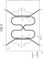
FIG. 2 shows a top view diagram of an optical switch according to the second embodiment. -
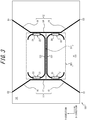
FIG. 3 shows a top view diagram of an optical switch according to the third embodiment. -
FIG. 4 shows a top view diagram of an optical switch according to the fourth embodiment. - Hereinafter, embodiments of an optical switch to which the present disclosure is applied will be described with reference to the drawings.
- As shown in
FIG. 1 , anoptical switch 10 according to the first embodiment of the present disclosure is configured to include afirst waveguide 11, asecond waveguide 12, and anexchanger 13. Thefirst waveguide 11, thesecond waveguide 12, and theexchanger 13 are provided on, for example, asubstrate 14. At least, thefirst waveguide 11 and thesecond waveguide 12 may be located on the same plane on thesubstrate 14. - The
substrate 14 may be made of, for example, a conductor such as metal, a semiconductor such as silicon, glass, or resin. In the present embodiment, any two directions perpendicular to each other on thesubstrate 14 are defined as x-direction and y-direction. - The
first waveguide 11 includes, for example, afirst end section 15, asecond end section 16, and a firstlinear section 17. The firstlinear section 17 is a linear section extending in the y-direction. The firstlinear section 17 connects to thefirst end section 15 at the opposite side end in the y-direction. The firstlinear section 17 is connected to thesecond end section 16 at the end in the y-direction side. The end of thefirst end section 15 on the opposite side in the y-direction is the first end E1, which is one end of the entirefirst waveguide 11. The end of thesecond end section 16 on the y-direction side is the second end E2, which is the other end of the entirefirst waveguide 11. The first end E1 and the second end E2 are ports where electromagnetic waves are input and output. - The
second waveguide 12 includes, for example, athird end section 18, afourth end section 19, and a secondlinear section 20. The secondlinear section 20 is a linear section extending in the y-direction. The secondlinear section 20 connects to thethird end section 18 at the opposite side end in the y-direction. The secondlinear section 20 is connected to thefourth end section 19 at the end on the y-direction side. The end of thethird end section 18 on the opposite side in the y-direction is the third end E3, which is one end of the entiresecond waveguide 12. The end of thefourth end section 19 on the y-direction side is the fourth end E4, which is one end of the entiresecond waveguide 12. Therefore, the third end E3 is located on the first end E1 side viewed from the center in the longitudinal direction of thefirst waveguide 11. Further, the fourth end E4 is located at the second end E2 side viewed from the center in the longitudinal direction of thefirst waveguide 11. The third end E3 and the fourth end E4 are ports where electromagnetic waves are input and output. - The
exchanger 13 comprises at least onefirst waveguide section 21 and at least onesecond waveguide section 22. - The
first waveguide section 21 is located along thefirst waveguide 11. Thefirst waveguide section 21 configures a 2×2 directional coupler together with thefirst waveguide 11. Thefirst waveguide section 21 comprises a firstphase change material 23. Thefirst waveguide section 21 may include a linear section extending in the y-direction. - The
second waveguide section 22 is located along thesecond waveguide 12. Thesecond waveguide section 22 configures a 2×2 directional coupler together with thesecond waveguide 12. Thesecond waveguide section 22 includes a secondphase change material 24. Thesecond waveguide section 22 may include a linear section extending in the y-direction. - The
first waveguide 11, thesecond waveguide 12, thefirst waveguide section 21, and thesecond waveguide section 22 are composed of a core and a clad. The cores of thefirst waveguide 11, thesecond waveguide 12, thefirst waveguide section 21, and thesecond waveguide section 22 may be made of the same dielectric material to propagate electromagnetic waves such as silicon. Further, the clad may be made of a dielectric with a smaller refractive index than the core, such as quartz glass. - At least a part of the first
linear section 17 is opposing to at least a part of the linear section of thefirst waveguide section 21. The length of the opposing part may be the coupling length in the state where the firstphase change material 23 is changed to the amorphous phase. The coupling length is the length from the starting point of the opposing part to the position where the coupling coefficient reaches its maximum value. The coupling coefficient is a parameter indicating the ratio of electromagnetic waves to be transferred from one waveguide to the other in a parallel waveguide in which two linear waveguides are lined up. In a configuration where no electromagnetic waves are transferred at all from one waveguide to the other, the coupling coefficient is zero. In a configuration where all electromagnetic waves are transferred from one waveguide to the other, the coupling coefficient is 1. The coupling coefficient is included in the range between 0 and 1. The coupling coefficient is determined based on the shape of each waveguide, the distance between each waveguide, or the length of the waveguides opposing to each other. - At least a part of the second
linear section 20 are opposing to at least a part of the linear section of thesecond waveguide section 22. The length of the opposing part may be the coupling length in the state where the secondphase change material 24 is changed to the amorphous phase. - The first
phase change material 23 and the secondphase change material 24 may be displaced from that same plane in a direction perpendicular to the same plane in which thefirst waveguide 11 and thesecond waveguide 12 are located. For example, the firstphase change material 23 and the secondphase change material 24 may each be located on the opposite side of thefirst waveguide section 21 and thesecond waveguide section 22 from thesubstrate 14 in a direction perpendicular to the main surface of thesubstrate 14, that is, the widest surface of thesubstrate 14. - The first
phase change material 23 and the secondphase change material 24 can be phase-changed to an amorphous or a crystalline phase. The firstphase change material 23 and the secondphase change material 24 may be phase-changed by laser beam emitted from a laser source or by heat generation by a resistive element. - When the first
phase change material 23 is an amorphous phase, loss of electromagnetic waves in thefirst waveguide section 21 is relatively small. Therefore, in this case, because the effective refractive indices of the firstlinear section 17 and thefirst waveguide section 21 are substantially the same and the length is also the coupling length, electromagnetic waves input from the first end E1 side of the firstlinear section 17 and thefirst waveguide section 21 are respectively output from the second end E2 side of thefirst waveguide section 21 and the firstlinear section 17. Similarly, when the secondphase change material 24 is an amorphous phase, electromagnetic waves input from the third end E3 side of the secondlinear section 20 and thesecond waveguide section 22 are respectively output from the fourth end E4 side of thesecond waveguide section 22 and the secondlinear section 20. - When the first
phase change material 23 is a crystalline phase, the loss of electromagnetic waves in thefirst waveguide section 21 is relatively large. Therefore, in this case, because the effective refractive indices of the firstlinear section 17 and thefirst waveguide section 21 are significantly different, the electromagnetic waves input from the first end E1 side of the firstlinear section 17 are not transferred to thefirst waveguide section 21, in other words, the electromagnetic waves are output from the second end E2 side of the firstlinear section 17 without propagating through the lossyfirst waveguide section 21. Similarly, if the secondphase change material 24 is a crystalline phase, electromagnetic waves input from the third end E3 side of the secondlinear section 20 are not transferred to thesecond waveguide section 22, but are output from the fourth end E4 side of the secondlinear section 20. - For the first
phase change material 23 and the secondphase change material 24, for example, tetrahedral materials such as amorphous silicon, amorphous germanium, amorphous gallium antimony, amorphous gallium arsenide, amorphous indium selenide, amorphous gallium selenide, Ge-Sb-Te chalcogenide materials such as Ge2Sb2Te5 and Ge6Sb2Te9, Sb-Te chalcogenide materials, or chalcogenide materials such as As2Se3, As2S3, are used. - The
exchanger 13 inputs electromagnetic waves, input from the first end E1 of thefirst waveguide 11 and output from any of thefirst waveguide sections 21 through a directional coupler, to the third end E3 side of any of thesecond waveguide sections 22. Theexchanger 13 inputs electromagnetic waves, input from the third end E3 of thesecond waveguide 12 and output from any of thesecond waveguide sections 22 through a directional coupler, to the first end E1 side of any of thefirst waveguide sections 21. - The
first waveguide 11, thesecond waveguide 12, and theexchanger 13 may satisfy the waveguiding condition in single mode. Therefore, electromagnetic waves, input to at least one of the first end E1 and the third end E3, may be propagated in single mode. - The detailed configuration of the
exchanger 13, as described above in the first embodiment, will be described below. - In the first embodiment, the
exchanger 13 comprises an annularthird waveguide 25 and an annularfourth waveguide 26. Thethird waveguide 25 and thefourth waveguide 26 are located, for example, between thefirst waveguide 11 and thesecond waveguide 12. Thethird waveguide 25 and thefourth waveguide 26 are arranged to line up along the x-direction, for example. - The
third waveguide 25 is annular including thefirst waveguide section 21 as a part. Thethird waveguide 25 has a linearfirst section 27 extending in the y-direction on the opposite side of thefirst waveguide section 21 in the x-direction. - The
fourth waveguide 26 is annular including thesecond waveguide section 22 as a part. Thefourth waveguide 26 has a linearsecond section 28 extending in the y-direction on the opposite side of thesecond waveguide section 22 in the x-direction. Thesecond section 28, that is a part of thefourth waveguide 26, is opposing to thefirst section 27, that is a part of thethird waveguide 25, and configures a 2×2 directional coupler. The length of thefirst section 27 and thesecond section 28 is the coupling length. Therefore, the electromagnetic waves, respectively input to thefirst section 27 and thesecond section 28, can be output from thesecond section 28 and thefirst section 27 at a higher intensity than the other sections. - The
optical switch 10 of the first embodiment, configured as described above, comprises: at least onefirst waveguide section 21 configuring a directional coupler together with thefirst waveguide 11 and including a firstphase change material 23; at least onesecond waveguide section 22 configuring a directional coupler together with asecond waveguide 12 and including a secondphase change material 24; and anexchanger 13, configured to: input electromagnetic waves, input from the first end E1 and output from any of thefirst waveguide sections 21, to the third end E3 side of any of thesecond waveguide sections 22; and to input electromagnetic waves, input from the third end E3 and output from any of thesecond waveguide sections 22, to the second end E2 side of any of the first waveguide sections 21.In such a configuration, when the phase of the firstphase change material 23 and the secondphase change material 24 is changed to a crystalline phase, theoptical switch 10 can cause electromagnetic waves, input to the first end E1 and the third end E3, to respectively output from the second end E2 and the fourth end E4 without causing them to propagate through thefirst waveguide section 21 and thesecond waveguide section 22. Further, when the phase of the firstphase change material 23 and the secondphase change material 24 are changed to an amorphous phase, theoptical switch 10 can cause electromagnetic waves, input to the first end E1 and the third end E3, to propagate through thefirst waveguide section 21 and thesecond waveguide section 22 in a state where the loss is relatively small, and to respectively output from the fourth end E4 and the second end E2. Therefore, in the crystal phases of the firstphase change material 23 and the secondphase change material 24 that relatively increase loss of electromagnetic waves in thefirst waveguide section 21 and thesecond waveguide section 22, theoptical switch 10 can switch the output destination of the electromagnetic waves without causing the electromagnetic waves to propagate through thefirst waveguide section 21 and thesecond waveguide section 22. Therefore, theoptical switch 10 can reduce insertion loss while using the firstphase change material 23 and the secondphase change material 24. - Further, in the
optical switch 10 of the first embodiment, electromagnetic waves, input to at least one of the first end E1 and the third end E3, are propagated in single mode. With such a configuration, theoptical switch 10 can be suitably used for optical communications because the waveform of the propagating signal is less likely to be collapsed. - Further, in the
optical switch 10 of the first embodiment, thefirst waveguide 11 and thesecond waveguide 12 are located on the same plane. In a configuration in which the same material is applied to thefirst waveguide 11 and thesecond waveguide 12, based on the above configuration, theoptical switch 10 can be easily produced on thesubstrate 14 as compared to the configuration in which both are displaced in the direction perpendicular to the main surface. - In the
optical switch 10 of the first embodiment, the firstphase change material 23 and the secondphase change material 24 are displaced from the same plane, in which thefirst waveguide 11 and thesecond waveguide 12 are located, in a direction perpendicular to the same plane. With such a configuration, theoptical switch 10 can form the firstphase change material 23 and the secondphase change material 24 in separate layers after forming the waveguides configurating thefirst waveguide 11, thesecond waveguide 12, and theexchanger 13. The waveguides configuring thefirst waveguide 11, thesecond waveguide 12, and theexchanger 13 can be made of the same material but different from the firstphase change material 23 and secondphase change material 24. Therefore, theoptical switch 10, configured as described above, can be easily produced by such a production method that layers are formed for each of the same materials. - Next, the optical switch according to the second embodiment of the present disclosure will be described. In the second embodiment, the configuration of the exchanger is different from that in the first embodiment. The second embodiment will be described below, focusing on the different points from the first embodiment. It is noted that the same reference signs are given to the parts with the same configuration as that in the first embodiment.
- As shown in
FIG. 2 , theoptical switch 100 according to the second embodiment is similar to that of the first embodiment and is configured to include afirst waveguide 11, asecond waveguide 12, and anexchanger 130. In the second embodiment, the configuration and function of thefirst waveguide 11 and thesecond waveguide 12 are the same as those in the first embodiment. - The
exchanger 130 comprises at least onefirst waveguide section 21 and at least onesecond waveguide section 22, as in the first embodiment. The configuration and function of thefirst waveguide section 21 and thesecond waveguide section 22 are the same as those in the first embodiment. - As in the first embodiment, the
exchanger 130 inputs electromagnetic waves, input from the first end E1 of thefirst waveguide 11 and output from any of thefirst waveguide sections 21 through a directional coupler, to the third end E3 side of any of thesecond waveguide sections 22. As in the first embodiment, theexchanger 130 inputs electromagnetic waves, input from the third end E3 of thesecond waveguide 12 and output from any of thesecond waveguide sections 22 through a directional coupler, to the first end E1 side of any of thefirst waveguide sections 21. - The detailed configuration of the
exchanger 130 as described above in the second embodiment will be described below. - In the second embodiment, the
exchanger 130 comprises an annularfifth waveguide 290. Thefifth waveguide 290 is located, for example, between thefirst waveguide 11 and thesecond waveguide 12. Thefifth waveguide 290 is annular, including afirst waveguide section 21 and asecond waveguide section 22 as a part. - In the
fifth waveguide 290, the second end E2 side of thefirst waveguide section 21 is connected to the third end E3 side of thesecond waveguide section 22 Further, in thefifth waveguide 290, the fourth end E4 side of thesecond waveguide section 22 is connected to the first end E1 side of thefirst waveguide section 21. Thefifth waveguide 290 has, for example, a shape in which an annulus is twisted by 180 degrees. - In the
fifth waveguide 290, a part of the linear section connecting the second end E2 side of thefirst waveguide section 21 to the third end E3 side of thesecond waveguide section 22 and a part of the linear section connecting the fourth end E4 side of thesecond waveguide section 22 to the first end E1 side of thefirst waveguide section 21 may be vertical. - Furthermore, a part of the linear section connecting the second end E2 side of the
first waveguide section 21 to the third end E3 side of thesecond waveguide section 22 and a part of the linear section connecting the fourth end E4 side of thesecond waveguide section 22 to the first end E1 side of thefirst waveguide section 21 may intersect, or be displaced in a direction perpendicular to the main surface of thesubstrate 14. - As in the first embodiment, the
optical switch 100 of the second embodiment, configured as described above, comprises: at least onefirst waveguide section 21 configuring a directional coupler together with thefirst waveguide 11 and including a firstphase change material 23; at least onesecond waveguide section 22 configuring a directional coupler together with thesecond waveguide 12 and including a secondphase change material 24; and anexchanger 130, configured to: input electromagnetic waves, input from the first end E1 and output from any of thefirst waveguide sections 21, to the third end E3 side of any of thesecond waveguide sections 22; and to input electromagnetic waves, input from the third end E3 and output from any of thesecond waveguide sections 22, to the second end E2 side of any of thefirst waveguide sections 21. Therefore, theoptical switch 100 of the second embodiment can also reduce insertion loss while using the firstphase change material 23 and the secondphase change material 24. Further, in theoptical switch 100 of the second embodiment, as in the first embodiment, electromagnetic waves, input to at least one of the first end E1 and the third end E3, is propagated in single mode. Therefore, theoptical switch 100 of the second embodiment can also be suitably used for optical communications because the waveform of the propagating signal is less likely to be collapsed. Further, in theoptical switch 100 of the second embodiment, as in the first embodiment, thefirst waveguide 11 and thesecond waveguide 12 are located on the same plane. In a configuration in which the same material is applied to thefirst waveguide 11 and thesecond waveguide 12, thanks to the configuration described above, theoptical switch 100 of the second embodiment can also be easily produced on thesubstrate 14 as compared to a configuration in which both are displaced in a direction perpendicular to the main plane. - In the
optical switch 100 of the second embodiment, as in the first embodiment, the firstphase change material 23 and the secondphase change material 24 are displaced from the same plane, in which thefirst waveguide 11 and thesecond waveguide 12 are located, in a direction perpendicular to the same plane. Therefore, theoptical switch 100 of the second embodiment can also be easily produced by the production method to form a layer for each of the same material. - Further, in the
optical switch 100 of the second embodiment, a part of the linear section connecting the second end E2 side of thefirst waveguide section 21 to the third end E3 side of thesecond waveguide section 22 and a part of the linear section connecting the fourth end E4 side of thesecond waveguide section 22 to the first end E1 side of thefirst waveguide section 21 are vertical. - With such a configuration, the
optical switch 100 can minimize that electromagnetic waves, propagating through a part of the linear section connecting the second end E2 side of thefirst waveguide section 21 to the third end E3 side of thesecond waveguide section 22, transfer to a part of the linear section connecting the fourth end E4 side of thesecond waveguide section 22 to the first end E1 side of thefirst waveguide section 21. - Next, the optical switch according to the third embodiment of the present disclosure will be described. In the third embodiment, the configuration of the exchanger is different from that in the first embodiment. The third embodiment will be described below, focusing on the different points from the first embodiment. It is noted that the same reference signs are given to the parts with the same configuration as that in the first embodiment.
- As shown in
FIG. 3 , theoptical switch 101 according to the third embodiment is similar to the first embodiment and is configured to include thefirst waveguide 11, thesecond waveguide 12, and theexchanger 131. In the third embodiment, the configuration and function of thefirst waveguide 11 and thesecond waveguide 12 are the same as those in the first embodiment. - The
exchanger 131 comprises at least onefirst waveguide section 21 and at least onesecond waveguide section 22, as in the first embodiment. The configuration and function of thefirst waveguide section 21 and thesecond waveguide section 22 are the same as those in the first embodiment. - As in the first embodiment, the
exchanger 131 inputs electromagnetic waves, input from the first end E1 of thefirst waveguide 11 and output from any of thefirst waveguide sections 21 through a directional coupler, to the third end E3 side of any of thesecond waveguide sections 22. Further, as in the first embodiment, theexchanger 131 inputs electromagnetic waves, input from the third end E3 of thesecond waveguide 12 and output from any of thesecond waveguide sections 22 through a directional coupler, to the first end E1 side of any of thefirst waveguide sections 21. - The detailed configuration of the
exchanger 131 as described above in the third embodiment will be described below. - In the third embodiment, the
exchanger 131 comprises asixth waveguide 301 and aseventh waveguide 311. Thesixth waveguide 301 and theseventh waveguide 311 are located, for example, between thefirst waveguide 11 and thesecond waveguide 12 Further, thesixth waveguide 301 and theseventh waveguide 311 are arranged so as to be arranged along the y-direction. Thesixth waveguide 301 is located on the opposite side in the y-direction, that is, on the first end E1 side or the third end E3 side. Further, theseventh waveguide 311 is located on the y-direction side, that is, on the second end E2 side or the fourth end E4 side. - The
exchanger 131 comprises twofirst waveguide sections 21 and twosecond waveguide sections 22. - The
sixth waveguide 301 comprises afirst waveguide section 21 on the first end E1 side and asecond waveguide section 22 on the third end E3 side. In thesixth waveguide 301, the second end E2 side of thefirst waveguide section 21 on the first end E1 side is connected to the fourth end E4 side of thesecond waveguide section 22 on the third end E3 side. Thesixth waveguide 301 comprises a linearthird section 321 extending in the x-direction between thefirst waveguide section 21 and thesecond waveguide section 22. - The
seventh waveguide 311 comprises afirst waveguide section 21 on the second end E2 side and asecond waveguide section 22 on the fourth end E4 side. In theseventh waveguide 311, the first end E1 side of thefirst waveguide section 21 on the second end E2 side is connected to the second end E2 side of thesecond waveguide section 22 on the fourth end E4 side. Theseventh waveguide 311 comprises a linearfourth section 331 extending in the x-direction between thefirst waveguide section 21 and thesecond waveguide section 22. Thefourth section 331, that is a part of theseventh waveguide 311, is opposing to thethird section 321, that is a part of thesixth waveguide 301, and configures a 2×2 directional coupler. The length of thethird section 321 and thefourth section 331 is the coupling length. Therefore, the electromagnetic waves, respectively input to thethird section 321 and thefourth section 331, can be output from thefourth section 331 and thethird section 321 at higher intensity than the other sections. - As in the first embodiment, the
optical switch 101 of the third embodiment, configured as described above, comprises: at least onefirst waveguide section 21 configuring a directional coupler together with thefirst waveguide 11 and including a firstphase change material 23; at least onesecond waveguide section 22 configuring a directional coupler together with thesecond waveguide 12 and including a secondphase change material 24; and anexchanger 131, configured: to input electromagnetic waves, input from the first end E1 and output from any of thefirst waveguide sections 21, to the third end E3 side of any of thesecond waveguide sections 22; and to input electromagnetic waves, input from the third end E3 and output from any of thesecond waveguide sections 22, to the second end E2 side of any of thefirst waveguide sections 21. Therefore, theoptical switch 101 of the third embodiment can also reduce insertion loss while using the firstphase change material 23 and the secondphase change material 24. Further, in theoptical switch 101 of the third embodiment, as in the first embodiment, the electromagnetic waves, input to at least one of the first end E1 and the third end E3, is propagated in single mode. Therefore, theoptical switch 101 of the third embodiment can also be suitably used for optical communications because the waveform of the propagating signal is less likely to be collapsed. Further, in theoptical switch 101 of the third embodiment, as in the first embodiment, thefirst waveguide 11 and thesecond waveguide 12 are located on the same plane. In a configuration in which the same material is applied to thefirst waveguide 11 and thesecond waveguide 12, thanks to the configuration described above, theoptical switch 101 of the third embodiment can also be easily produced on thesubstrate 14 as compared to a configuration in which both are displaced in a direction perpendicular to the main plane. Further, in theoptical switch 101 of the third embodiment, as in the first embodiment, - the first
phase change material 23 and the secondphase change material 24 are displaced from the same plane, in which thefirst waveguide 11 and thesecond waveguide 12 are located, in a direction perpendicular to the same plane. Therefore, theoptical switch 101 of the third embodiment can also be easily produced by the production method to form a layer for each of the same material. - Next, the optical switch according to the fourth embodiment of the present disclosure will be described. In the fourth embodiment, the configuration of the exchanger is different from that in the first embodiment. Hereinafter, the fourth embodiment will be described below, focusing on the different points from the first embodiment. It is noted that the same reference signs are given to the parts with the same configuration as that in the first embodiment.
- As shown in
FIG. 4 , theoptical switch 102 according to the fourth embodiment is similar to the first embodiment and is configured to include thefirst waveguide 11, thesecond waveguide 12, and theexchanger 132. In the fourth embodiment, the configuration and function of thefirst waveguide 11 and thesecond waveguide 12 are the same as those in the first embodiment. - The
exchanger 132 comprises at least onefirst waveguide section 21 and at least onesecond waveguide section 22, as in the first embodiment. The configuration and function of thefirst waveguide section 21 and thesecond waveguide section 22 are the same as those in the first embodiment. - As in the first embodiment, the
exchanger 132 inputs electromagnetic waves, input from the first end E1 of thefirst waveguide 11 and output from any of thefirst waveguide sections 21 through a directional coupler, to the third end E3 side of any of thesecond waveguide sections 22. Further, as in the first embodiment, theexchanger 13 inputs electromagnetic waves, input from the third end E3 of thesecond waveguide 12 and output from any of thesecond waveguide sections 22 through a directional coupler, to the first end E1 side of any of thefirst waveguide sections 21. - The detailed configuration of the
exchanger 132 as described above in the fourth embodiment will be described below. - In a fourth embodiment, the
exchanger 132 comprises aneighth waveguide 342 and aninth waveguide 352. Theeighth waveguide 342 and theninth waveguide 352 are located, for example, between thefirst waveguide 11 and thesecond waveguide 12. - The
exchanger 132 comprises twofirst waveguide sections 21 and twosecond waveguide sections 22. - The
eighth waveguide 342 comprises afirst waveguide section 21 on the first end E1 side and asecond waveguide section 22 on the fourth end E4 side. In theeighth waveguide 342, the second end E2 side of thefirst waveguide section 21 on the first end E1 side is connected to the third end E3 side of thesecond waveguide section 22 on the fourth end E4 side. - The
ninth waveguide 352 comprises afirst waveguide section 21 on the second end E2 side and asecond waveguide section 22 on the third end E3 side. In theninth waveguide 352, the first end E1 side of thefirst waveguide section 21 on the second end E2 side is connected to the fourth end E4 side of thesecond waveguide section 22 on the third end E3 side. - A part of the linear section connecting the second end E2 side of the
first waveguide section 21 to the third end E3 side of thesecond waveguide section 22 in theeighth waveguide 342 and a part of the linear section connecting the first end E1 side of thefirst waveguide section 21 to the fourth end E4 side of thesecond waveguide section 22 in theninth waveguide 352 are intersected as viewed from a direction perpendicular to the main plane of thesubstrate 14. Further, the intersection part of theeighth waveguide 342 and theninth waveguide 352 as viewed from the direction perpendicular to the main surface of thesubstrate 14 may be vertical. The intersection part of theeighth waveguide 342 and theninth waveguide 352 as viewed from the direction perpendicular to the main surface of thesubstrate 14 may intersect, or may be displaced in the direction perpendicular to the main surface of thesubstrate 14. - As in the first embodiment, the
optical switch 102 of the fourth embodiment, configured as described above, comprises: at least onefirst waveguide section 21 configuring a directional coupler together with thefirst waveguide 11 and including a firstphase change material 23; at least onesecond waveguide section 22 configuring a directional coupler together with thesecond waveguide 12 and including a secondphase change material 24; and - an
exchanger 132, configured: to input electromagnetic waves, input from the first end E1 and output from any of thefirst waveguide sections 21, to the third end E3 side of any of thesecond waveguide sections 22; and to input electromagnetic waves, input from the third end E3 and output from any of thesecond waveguide sections 22, to the second end E2 side of any of thefirst waveguide sections 21. Therefore, theoptical switch 102 of the fourth embodiment can also reduce insertion loss while using the firstphase change material 23 and the secondphase change material 24. Further, in theoptical switch 102 of the fourth embodiment, as in the first embodiment, the electromagnetic waves, input to at least one of the first end E1 and the third end E3, is propagated in single mode. Therefore, theoptical switch 102 of the fourth embodiment can also be suitably used for optical communications because the waveform of the propagating signal is less likely to be collapsed. Further, in theoptical switch 102 of the fourth embodiment, as in the first embodiment, thefirst waveguide 11 and thesecond waveguide 12 are located on the same plane. In a configuration in which the same material is applied to thefirst waveguide 11 and thesecond waveguide 12, thanks to the configuration described above, theoptical switch 102 of the fourth embodiment can also be easily produced on thesubstrate 14 as compared to a configuration in which both are displaced in a direction perpendicular to the main plane. Further, in theoptical switch 102 of the fourth embodiment, as in the first embodiment, - the first
phase change material 23 and the secondphase change material 24 are displaced from the same plane, in which thefirst waveguide 11 and thesecond waveguide 12 are located, in a direction perpendicular to the same plane. Therefore, theoptical switch 102 of the fourth embodiment can also be easily produced by the production method to form a layer for each of the same material. - Further, in the
optical switch 102 of the fourth embodiment, a part of the linear section connecting the second end E2 side of thefirst waveguide section 21 to the third end E3 side of thesecond waveguide section 22 in theeighth waveguide 342, and a part of the linear section connecting the first end E1 side of thefirst waveguide section 21 to the fourth end E4 side of thesecond waveguide section 22 in theninth waveguide 352 are vertical. With such a configuration, theoptical switch 102 of the fourth embodiment can minimize that electromagnetic waves, propagating through a part of the linear section connecting the second end E2 side of thefirst waveguide section 21 to the third end E3 side of thesecond waveguide section 22, transfer to a part of the linear section connecting the fourth end E4 side of thesecond waveguide section 22 to the first end E1 side of thefirst waveguide section 21. - The present disclosure has been described with reference to the drawings and examples. It should be noted that those skilled in the art can easily make various variations and modifications based on the present disclosure. Therefore, it should be noted that these variations and modifications are included in the scope of the present disclosure.
- For example, in the first through fourth embodiments, the
optical switches single exchanger exchangers - Further, in the first embodiment, the
exchanger 13 is configured to comprise two annular waveguides, athird waveguide 25 and afourth waveguide 26. However, the same effect as that in the first embodiment can be obtained - even if the
exchanger 13 is formed so that an even number of annular waveguides, adjacent to each other in the x direction, configure a 2 × 2 directional coupler between thethird waveguide 25 and thefourth waveguide 26. - Further, in the third embodiment and the fourth embodiment, the
exchangers first waveguide sections 21 and twosecond waveguide sections 22. However, theexchangers first waveguide sections 21 and three or moresecond waveguide sections 22. In the third embodiment, thesixth waveguide 301 may include thefirst waveguide section 21 other than the one located on most second end E2 side among the plurality offirst waveguide sections 21, and thesecond waveguide section 22 other than the one located on most fourth end E4 side among the plurality ofsecond waveguide sections 22. In the fourth embodiment, theeighth waveguide 342 may include thefirst waveguide section 21 other than the one located on most second end E2 side among the plurality offirst waveguide sections 21, and thesecond waveguide section 22 other than the one located on most third end E3 side among the plurality ofsecond waveguide sections 22. - 10, 100, 101, 102 Optical switch
- 11 First waveguide
- 12 Second waveguide
- 13, 130, 131, 132 Exchanger
- 14 Substrate
- 15 First end section
- 16 Second end section
- 17 First linear section
- 18 Third end section
- 19 Fourth end section
- 20 Second linear section
- 21 First waveguide section
- 22 Second waveguide section
- 23 First phase change material
- 24 Second phase change material
- 25 Third waveguide
- 26 Fourth waveguide
- 27 First section
- 28 Second section
- 290 Fifth waveguide
- 301 Sixth waveguide
- 311 Seventh waveguide
- 321 Third section
- 331 Fourth section
- 342 Eighth waveguide
- 352 Ninth waveguide
- E1, E2, E3, E4 First end, Second end, Third end, Fourth end
Claims (12)
- An optical switch comprising:a first waveguide comprising a first end and a second end which are ports electromagnetic waves are input to and output from;a second waveguide comprising a third end and a fourth end which are ports electromagnetic waves are input to and output from, wherein the third end and the fourth end are located on the first end side and the second end side, respectively, as viewed from the center of the first waveguide; andan exchanger comprising: at least one first waveguide section, located along the first waveguide, configuring a directional coupler together with the first waveguide, and including a phase change material; and at least one second waveguide section, located along the second waveguide, configuring a directional coupler together with the second waveguide, and including a phase change material, wherein the exchanger inputs electromagnetic waves, input from the first end and output from any of the first waveguide sections, to a third end side of any of the second waveguide sections; and the exchanger inputs electromagnetic waves, input from the third end and output from any of the second waveguide sections, to a second end side of any of the first waveguide sections.
- The optical switch, according to claim 1,
wherein the exchanger comprises an annular third waveguide including the first waveguide section, and an annular fourth waveguide configuring a directional coupler together with a part of the third waveguide and including the second waveguide section. - The optical switch, according to claim 1,
wherein the exchanger comprises an annular fifth waveguide including the first waveguide section and the second waveguide section, and in the fifth waveguide the second end side of the first waveguide section is connected to the third end side of the second waveguide section and the fourth end side of the second waveguide section is connected to the first end side of the first waveguide section. - The optical switch, according to claim 3,
wherein in the fifth waveguide, a part of a linear section connecting the second end side of the first waveguide section to the third end side of the second waveguide section, and a part of a linear section connecting the fourth end side of the second waveguide section to the first end side of the first waveguide section are vertical. - The optical switch, according to claim 1,
wherein the exchanger comprises:a sixth waveguide including any of the first waveguide sections among a plurality of first waveguide sections, and any of the second waveguide sections among a plurality of second waveguide sections, the second end side of the first waveguide sections being connected to the fourth end side of the any of the second waveguide section; anda seventh waveguide, located on the second end side from the sixth waveguide, configuring a directional coupler together with a part of the sixth waveguide, and including: the first waveguide section located at the second end side from the first waveguide section; and the second waveguide section located at the fourth end side from the second waveguide section, the first end side of the first waveguide section being connected to the third end side of the second waveguide section. - The optical switch, according to claim 1,
wherein the exchanger comprises:an eighth waveguide including: any of the first waveguide sections among a plurality of the first waveguide sections; and any of the second waveguide sections among a plurality of the second waveguide sections, the second end side of the first waveguide sections being connected to the third end side of the second waveguide section; anda ninth waveguide including the first waveguide section located at the second end side from the first waveguide section, and the second waveguide section located at the third end side from the second waveguide section, the first end side of the first waveguide section being connected to the fourth end side of the second waveguide section. - The optical switch, according to claim 6,
wherein a part of a linear section connecting the second end side of the first waveguide section to the third end side of the second waveguide section in the eighth waveguide, and a part of a linear section connecting the first end side of the first waveguide section to the fourth end side of the second waveguide section in the ninth waveguide are vertical. - The optical switch, according to any one of claims 1 to 7, wherein laser beam is used for phase change of the phase change material.
- The optical switch, according to any one of claims 1 to 7, wherein heat generation by resistive elements is used for phase change of the phase change material.
- The optical switch, according to any one of claims 1 to 9, wherein electromagnetic waves, input to at least one of the first end and the third end, are propagated in single mode.
- The optical switch, according to any one of claims 1 to 10,
wherein the first waveguide and the second waveguide are located on the same plane. - The optical switch, according to claim 11, wherein the phase change material is displaced from the plane in the direction perpendicular to the same plane.
Applications Claiming Priority (2)
| Application Number | Priority Date | Filing Date | Title |
|---|---|---|---|
| JP2018222732A JP7123769B2 (en) | 2018-11-28 | 2018-11-28 | light switch |
| PCT/JP2019/043330 WO2020110628A1 (en) | 2018-11-28 | 2019-11-05 | Optical switch |
Publications (2)
| Publication Number | Publication Date |
|---|---|
| EP3889679A1 true EP3889679A1 (en) | 2021-10-06 |
| EP3889679A4 EP3889679A4 (en) | 2022-10-26 |
Family
ID=70854281
Family Applications (1)
| Application Number | Title | Priority Date | Filing Date |
|---|---|---|---|
| EP19888928.9A Pending EP3889679A4 (en) | 2018-11-28 | 2019-11-05 | Optical switch |
Country Status (5)
| Country | Link |
|---|---|
| US (1) | US11782219B2 (en) |
| EP (1) | EP3889679A4 (en) |
| JP (1) | JP7123769B2 (en) |
| CN (1) | CN113168065B (en) |
| WO (1) | WO2020110628A1 (en) |
Family Cites Families (20)
| Publication number | Priority date | Publication date | Assignee | Title |
|---|---|---|---|---|
| US5002354A (en) * | 1989-10-16 | 1991-03-26 | Gte Laboratories Incorporated | High-extinction 2×2 integrated optical changeover switches |
| US6947632B2 (en) * | 2002-01-03 | 2005-09-20 | Fischer Sylvain G | Method of implementing the kerr effect in an integrated ring resonator (the kerr integrated optical ring filter) to achieve all-optical wavelength switching, as well as all-optical tunable filtering, add-and -drop multiplexing, space switching and optical intensity modulation |
| JP2003337317A (en) * | 2002-05-17 | 2003-11-28 | Nippon Sheet Glass Co Ltd | Waveguide type liquid crystal optical switch |
| US6847741B2 (en) * | 2002-10-04 | 2005-01-25 | Lockheed Martin Corp | Optically induced total internal reflection X-junction waveguide optical switch, network and optical switching method |
| US7145660B2 (en) * | 2003-08-13 | 2006-12-05 | Lambda Crossing, Ltd. | Micro-resonator based optical sensor |
| JP2005077943A (en) * | 2003-09-02 | 2005-03-24 | Fdk Corp | Optical waveguide device and manufacturing method thereof |
| US7123800B2 (en) * | 2004-03-02 | 2006-10-17 | Celight, Inc. | Integrated loop resonator with adjustable couplings and methods of using the same |
| JP2006184345A (en) | 2004-12-27 | 2006-07-13 | Keio Gijuku | Optical switch, optical serial-parallel converter, parallel bit delay variable / wavelength conversion circuit, and optical time switch |
| JP4395572B2 (en) * | 2007-04-13 | 2010-01-13 | 株式会社エスシーエー | Tactile information transmission device using mechanical vibration of shape memory alloy as information transmission means |
| US8488922B2 (en) * | 2007-11-02 | 2013-07-16 | Infinera Corporation | Multi-channel dispersion compensator |
| JP5083732B2 (en) | 2007-11-26 | 2012-11-28 | 学校法人慶應義塾 | Light switch |
| KR100999547B1 (en) * | 2008-07-07 | 2010-12-08 | 중앙대학교 산학협력단 | Wideband Tunable Laser Diode |
| KR101381900B1 (en) * | 2010-10-01 | 2014-04-04 | 한국전자통신연구원 | Method of tuning the resonance wavelength ring resonator |
| US8494323B2 (en) * | 2010-11-29 | 2013-07-23 | Octrolix Bv | Optical system having a symmetrical coupling region for coupling light between waveguides including an optically resonant element |
| EP2745154A4 (en) * | 2011-08-18 | 2015-07-01 | Opel Solar Inc | OPTICAL CLOSED LOOP MICRORESONATOR AND THYRISTOR MEMORY DEVICE |
| CN106471634B (en) | 2014-07-02 | 2018-11-27 | 三井化学株式会社 | The manufacturing method of high polymer piezoelectric material, lamilate, the manufacturing method of high polymer piezoelectric material and lamilate |
| US9746746B2 (en) * | 2014-08-01 | 2017-08-29 | Mohammad A Mazed | Fast optical switch and its applications in optical communication |
| JP6509509B2 (en) * | 2014-08-21 | 2019-05-08 | ルネサスエレクトロニクス株式会社 | Optical semiconductor device and method of manufacturing the same |
| GB2530345A (en) * | 2014-09-22 | 2016-03-23 | Mastercard International Inc | Payment systems and methods for managing payment card use |
| US10353267B2 (en) * | 2016-12-30 | 2019-07-16 | Huawei Technologies Co., Ltd. | Carrier-effect based optical switch |
-
2018
- 2018-11-28 JP JP2018222732A patent/JP7123769B2/en active Active
-
2019
- 2019-11-05 CN CN201980078464.5A patent/CN113168065B/en active Active
- 2019-11-05 EP EP19888928.9A patent/EP3889679A4/en active Pending
- 2019-11-05 WO PCT/JP2019/043330 patent/WO2020110628A1/en not_active Ceased
- 2019-11-05 US US17/297,113 patent/US11782219B2/en active Active
Also Published As
| Publication number | Publication date |
|---|---|
| US20210396934A1 (en) | 2021-12-23 |
| JP2020086243A (en) | 2020-06-04 |
| US11782219B2 (en) | 2023-10-10 |
| CN113168065A (en) | 2021-07-23 |
| JP7123769B2 (en) | 2022-08-23 |
| CN113168065B (en) | 2024-07-19 |
| WO2020110628A1 (en) | 2020-06-04 |
| EP3889679A4 (en) | 2022-10-26 |
Similar Documents
| Publication | Publication Date | Title |
|---|---|---|
| EP3545346B1 (en) | Optical edge coupler with controllable mode field for photonic chip | |
| US8718423B2 (en) | Optical branching element and optical branching circuit | |
| US20080193079A1 (en) | Interface Device For Performing Mode Transformation in Optical Waveguides | |
| EP4062213A1 (en) | Electrically-controllable 3d optical waveguide switch with phase change materials | |
| CN111819480B (en) | Photonic device for converting optical modes of a light beam | |
| WO2016047079A1 (en) | Optical circuit element and optical circuit element configuration method | |
| WO2018135429A1 (en) | Crossing optical waveguide structure and optical waveguide element | |
| JP6798313B2 (en) | Rib-type optical waveguide and optical waveguide using it | |
| JP2015169766A (en) | polarization rotation circuit | |
| CN108227075B (en) | Curved waveguide structure and polarization beam splitting rotator | |
| CN113985522A (en) | Micro-ring optical switch based on silicon-silicon nitride three-dimensional integration | |
| JPH04212108A (en) | Waveguide type light branching element | |
| US11782219B2 (en) | Optical switch | |
| Li et al. | Single-point tunable and non-volatile Y-junction photonic power splitter on SOI with broadband and low loss | |
| Luo et al. | Inverse design of deformed Sb2Se3 stripes in silicon waveguide for reconfigurable mode converters | |
| JP5504476B2 (en) | Optical waveguide crossing structure | |
| Mandal et al. | Reconfigurable phase change chalcogenide grating couplers with ultrahigh modulation contrast | |
| US20230280524A1 (en) | Optical Waveguide Device and Method for Manufacturing the Same | |
| JP5759039B1 (en) | Optical coupling structure | |
| JP2015191029A (en) | spot size converter | |
| Middleton | Photonic waveguides shed their cladding | |
| Cui et al. | Mode multiplexing 1× 4 waveguide optical switch based on phase-change materials | |
| Trung et al. | Numerical Design of a Waveguide Crossing Based on SOI platform for Wideband Photonic Integrated Circuits and Networks | |
| Wu et al. | Theoretical study of Si₃N₄-based 4× 4 star coupler and edge coupler operating at 850nm | |
| JP6663145B2 (en) | Optical directional coupler |
Legal Events
| Date | Code | Title | Description |
|---|---|---|---|
| STAA | Information on the status of an ep patent application or granted ep patent |
Free format text: STATUS: THE INTERNATIONAL PUBLICATION HAS BEEN MADE |
|
| PUAI | Public reference made under article 153(3) epc to a published international application that has entered the european phase |
Free format text: ORIGINAL CODE: 0009012 |
|
| STAA | Information on the status of an ep patent application or granted ep patent |
Free format text: STATUS: REQUEST FOR EXAMINATION WAS MADE |
|
| 17P | Request for examination filed |
Effective date: 20210527 |
|
| AK | Designated contracting states |
Kind code of ref document: A1 Designated state(s): AL AT BE BG CH CY CZ DE DK EE ES FI FR GB GR HR HU IE IS IT LI LT LU LV MC MK MT NL NO PL PT RO RS SE SI SK SM TR |
|
| DAV | Request for validation of the european patent (deleted) | ||
| DAX | Request for extension of the european patent (deleted) | ||
| A4 | Supplementary search report drawn up and despatched |
Effective date: 20220923 |
|
| RIC1 | Information provided on ipc code assigned before grant |
Ipc: G02F 1/01 20060101ALI20220919BHEP Ipc: G02B 6/12 20060101ALI20220919BHEP Ipc: G02F 1/313 20060101AFI20220919BHEP |
|
| P01 | Opt-out of the competence of the unified patent court (upc) registered |
Effective date: 20230508 |
|
| STAA | Information on the status of an ep patent application or granted ep patent |
Free format text: STATUS: EXAMINATION IS IN PROGRESS |
|
| 17Q | First examination report despatched |
Effective date: 20240521 |