EP3889625A1 - Battery current measuring device and method - Google Patents
Battery current measuring device and method Download PDFInfo
- Publication number
- EP3889625A1 EP3889625A1 EP20736203.9A EP20736203A EP3889625A1 EP 3889625 A1 EP3889625 A1 EP 3889625A1 EP 20736203 A EP20736203 A EP 20736203A EP 3889625 A1 EP3889625 A1 EP 3889625A1
- Authority
- EP
- European Patent Office
- Prior art keywords
- switching element
- voltage
- battery
- temperature
- current measuring
- Prior art date
- Legal status (The legal status is an assumption and is not a legal conclusion. Google has not performed a legal analysis and makes no representation as to the accuracy of the status listed.)
- Granted
Links
Images


Classifications
-
- G—PHYSICS
- G01—MEASURING; TESTING
- G01R—MEASURING ELECTRIC VARIABLES; MEASURING MAGNETIC VARIABLES
- G01R31/00—Arrangements for testing electric properties; Arrangements for locating electric faults; Arrangements for electrical testing characterised by what is being tested not provided for elsewhere
- G01R31/36—Arrangements for testing, measuring or monitoring the electrical condition of accumulators or electric batteries, e.g. capacity or state of charge [SoC]
- G01R31/382—Arrangements for monitoring battery or accumulator variables, e.g. SoC
- G01R31/3842—Arrangements for monitoring battery or accumulator variables, e.g. SoC combining voltage and current measurements
-
- G—PHYSICS
- G01—MEASURING; TESTING
- G01R—MEASURING ELECTRIC VARIABLES; MEASURING MAGNETIC VARIABLES
- G01R19/00—Arrangements for measuring currents or voltages or for indicating presence or sign thereof
- G01R19/0092—Measuring current only
-
- G—PHYSICS
- G01—MEASURING; TESTING
- G01R—MEASURING ELECTRIC VARIABLES; MEASURING MAGNETIC VARIABLES
- G01R19/00—Arrangements for measuring currents or voltages or for indicating presence or sign thereof
- G01R19/25—Arrangements for measuring currents or voltages or for indicating presence or sign thereof using digital measurement techniques
-
- G—PHYSICS
- G01—MEASURING; TESTING
- G01R—MEASURING ELECTRIC VARIABLES; MEASURING MAGNETIC VARIABLES
- G01R31/00—Arrangements for testing electric properties; Arrangements for locating electric faults; Arrangements for electrical testing characterised by what is being tested not provided for elsewhere
- G01R31/36—Arrangements for testing, measuring or monitoring the electrical condition of accumulators or electric batteries, e.g. capacity or state of charge [SoC]
- G01R31/374—Arrangements for testing, measuring or monitoring the electrical condition of accumulators or electric batteries, e.g. capacity or state of charge [SoC] with means for correcting the measurement for temperature or ageing
-
- H—ELECTRICITY
- H02—GENERATION; CONVERSION OR DISTRIBUTION OF ELECTRIC POWER
- H02J—ELECTRIC POWER NETWORKS; CIRCUIT ARRANGEMENTS OR SYSTEMS FOR SUPPLYING OR DISTRIBUTING ELECTRIC POWER; SYSTEMS FOR STORING ELECTRIC ENERGY
- H02J7/00—Circuit arrangements for charging or discharging batteries or for supplying loads from batteries
- H02J7/80—Circuit arrangements for charging or discharging batteries or for supplying loads from batteries including monitoring or indicating arrangements
-
- H—ELECTRICITY
- H02—GENERATION; CONVERSION OR DISTRIBUTION OF ELECTRIC POWER
- H02J—ELECTRIC POWER NETWORKS; CIRCUIT ARRANGEMENTS OR SYSTEMS FOR SUPPLYING OR DISTRIBUTING ELECTRIC POWER; SYSTEMS FOR STORING ELECTRIC ENERGY
- H02J7/00—Circuit arrangements for charging or discharging batteries or for supplying loads from batteries
- H02J7/90—Regulation of charging or discharging current or voltage
- H02J7/933—Regulation of charging or discharging current or voltage the cycle being controlled or terminated in response to electric parameters
-
- G—PHYSICS
- G01—MEASURING; TESTING
- G01R—MEASURING ELECTRIC VARIABLES; MEASURING MAGNETIC VARIABLES
- G01R19/00—Arrangements for measuring currents or voltages or for indicating presence or sign thereof
- G01R19/32—Compensating for temperature change
-
- G—PHYSICS
- G01—MEASURING; TESTING
- G01R—MEASURING ELECTRIC VARIABLES; MEASURING MAGNETIC VARIABLES
- G01R31/00—Arrangements for testing electric properties; Arrangements for locating electric faults; Arrangements for electrical testing characterised by what is being tested not provided for elsewhere
- G01R31/36—Arrangements for testing, measuring or monitoring the electrical condition of accumulators or electric batteries, e.g. capacity or state of charge [SoC]
- G01R31/392—Determining battery ageing or deterioration, e.g. state of health
-
- Y—GENERAL TAGGING OF NEW TECHNOLOGICAL DEVELOPMENTS; GENERAL TAGGING OF CROSS-SECTIONAL TECHNOLOGIES SPANNING OVER SEVERAL SECTIONS OF THE IPC; TECHNICAL SUBJECTS COVERED BY FORMER USPC CROSS-REFERENCE ART COLLECTIONS [XRACs] AND DIGESTS
- Y02—TECHNOLOGIES OR APPLICATIONS FOR MITIGATION OR ADAPTATION AGAINST CLIMATE CHANGE
- Y02E—REDUCTION OF GREENHOUSE GAS [GHG] EMISSIONS, RELATED TO ENERGY GENERATION, TRANSMISSION OR DISTRIBUTION
- Y02E60/00—Enabling technologies; Technologies with a potential or indirect contribution to GHG emissions mitigation
- Y02E60/10—Energy storage using batteries
Definitions
- the present invention relates to a battery current measuring device and method.
- the present invention relates to a device and method for measuring battery current without using a shunt resistor.
- the charge/discharge current of the battery must be measured to calculate/compute not only the output but also battery information such as battery degeneration information and battery capacity.
- precise measurement accuracy is required in order to accurately calculate the battery information, and in order to meet this, conventionally, a battery current is measured using a precision resistor such as a shunt.
- an object of the present invention is to obtain an efficient battery current measuring means without using a shunt resistor that occupies a large volume and adds cost and assembly process.
- a battery current measuring device includes: a switching element configured to control charging and discharging of a battery: an A/D converter configured to convert a voltage value across the switching element into a digital value; a temperature compensation unit having a diode structure capable of compensating for a resistance change according to a change of temperature of the switching element; and a current calculation unit configured to calculate a current flowing through the switching element based on the digital value of the voltage value, and the A/D converter converts the voltage value of the switching element into the digital value using a reference voltage inputted from the temperature compensation unit.
- the diode structure of the temperature compensation unit includes a plurality of diodes, and a number and connection configuration of the plurality of diodes are determined so as to have a temperature-resistance curve matching a temperature-resistance curve of the switching element.
- the battery current measuring device further includes a voltage amplification unit configured to amplify the voltage value before applying the voltage value across the switching element to the A/D converter.
- the reference voltage is changed according to the diode structure and the temperature.
- the temperature compensation unit is disposed close to the switching element.
- the switching element is a MOSFET.
- the temperature compensation unit is formed on a same layer as a layer on which the MOSFET is formed on a substrate on which the battery current measuring device is installed.
- a battery current measuring method includes: receiving a voltage across a switching element for controlling charging and discharging of a battery; generating a reference voltage for compensating for a resistance change according to a temperature change of the switching element; converting the voltage of the switching element into a digital value using the generated reference voltage; and calculating a current flowing through the switching element based on the digital value.
- a battery pack includes: a battery capable of being charged and discharged; a switching element configured to control charging and discharging of the battery: an A/D converter configured to convert a voltage value across the switching element into a digital value; a temperature compensation unit having a diode structure capable of compensating for a resistance change according to a temperature change of the switching element; and a current calculation unit configured to calculate a current flowing through the switching element based on the digital value of the voltage value, and the A/D converter converts the voltage value of the switching element into the digital value using a reference voltage inputted from the temperature compensation unit.
- a battery current measuring device includes: a switching element configured to control charging and discharging of a battery: an A/D converter configured to convert a voltage across the switching element into a digital value; a temperature compensation unit including a diode structure that has a temperature-resistance curve matching the switching element and is capable of compensating for a resistance change according to a temperature change of the switching element; a subtractor configured to receive the voltage across the switching element and an output of the temperature compensation unit and output a constant voltage signal; and a current calculation unit configured to calculate a current flowing through the switching element based on the digital value of the voltage, and the A/D converter converts the voltage signal inputted from the subtractor into the digital value using a fixed reference voltage.
- the present invention is to measure the current of the battery using a semiconductor switch to turn on/off the battery without using a shunt resistor so that the volume can be reduced and it is more efficient in terms of cost and production process.
- the present invention includes a method and device that can measure current using essential components of the battery to measure the current of the battery without using a shunt resistor.
- a switching element for controlling charging and discharging by turning on/off a battery must be essentially present, and the switching element is composed of a semiconductor device such as a MOSFET.
- the present invention includes the diode configuration as described below, thereby making it possible to accurately measure the current of the battery by supplementing the difficulty of accurate current measurement according to the resistance change of the MOSFET with temperature.
- the configuration of the present invention will be described in more detail.
- the type of battery is not particularly limited, and for example, the battery may be composed of a lithium ion battery, a lithium polymer battery, a nickel cadmium battery, a nickel hydrogen battery, a nickel zinc battery, and the like.
- a plurality of battery cells are formed of a battery module connected in series and/or parallel, and at least one battery module is combined with a Battery Management System (BMS) to form a battery pack.
- BMS Battery Management System
- the BMS estimates the state of the battery and manages the battery using the estimated state information.
- the battery cell or battery module will be referred to simply as a battery.
- FIG. 1 is a view briefly comparing a conventional battery current measuring device with a battery current measuring device according to an embodiment of the present invention.
- FIG. 1 the view on the left side is a simplified diagram of a battery current measuring device for measuring current of a battery using a conventional shunt resistor.
- a shunt resistor is connected in series on one side of the battery, and the BMS calculates the battery current by measuring the voltage across the connected shunt resistor.
- the battery current measuring method through the shunt resistor will be described in more detail.
- a shunt resistor is connected in series on one side of the battery and the voltage across the shunt resistor is measured by a voltage measurement unit.
- the voltage across the shunt resistor is amplified by the voltage amplification unit because of its small size.
- the voltage amplified by the voltage amplification unit is converted to a digital value through an analog to digital (A/D) converter.
- A/D analog to digital
- the reference voltage of the A/D converter may be a fixed value, for example, 5 V.
- the digital signal converted by the A/D converter is transmitted to the MCU.
- the current of the battery is calculated using the received digital signal.
- the voltage measurement unit the voltage amplification unit, the A/D converter, and the MCU are included in the Battery Management System (BMS).
- BMS Battery Management System
- a switching element for controlling charging and discharging of the battery is located on the current path between the battery and the output terminal.
- the switching element is generally a semiconductor device, preferably a MOSFET.
- the switching element receives the control signal from the BMS to perform charging and discharging of the battery.
- FIG. 1 the view on the right side is a simplified diagram of a battery current measuring device according to an embodiment of the present invention.
- the battery current measuring device does not include a shunt resistor unlike a conventional battery current measuring device.
- a battery current is calculated by using a switching element, for example, a MOSFET, for controlling charging and discharging of the battery.
- a switching element for example, a MOSFET
- the voltage across the MOSFET is measured by the voltage measurement unit.
- MOSFETs are semiconductor devices, and the resistance changes greatly with the change in temperature.
- the MOSFET is directly connected to the battery because it performs charging/discharging control of the battery, and because of the heat generated during battery charging/discharging, MOSFETs are also affected by battery heat. Therefore, it is difficult to accurately measure the voltage of the MOSFET as the resistance changes due to the heat of the MOSFET.
- the present invention includes a separate temperature compensation unit to compensate for the resistance change caused by the heat of the MOSFET. This will be described later.
- the voltage measured across the MOSFET is amplified by the voltage amplification unit.
- the amplified signal is converted into a digital signal by the A/D converter. That is, the A/D converter converts the voltage across the switching element into a digital value.
- the reference voltage of the A/D converter is changed.
- a diode structure is connected to the A/D converter.
- the diode structure may be composed of a single or a plurality of diodes.
- the diode connected to the A/D converter is selected to have the same voltage drop characteristic as the MOSFET, or a plurality of diodes are connected in series and in parallel to allow the temperature curve to be the same as that of the MOSFET. That is, the plurality of diodes have a temperature-resistance curve that matches the temperature-resistance curve of the MOSFET which is the switching element.
- the temperature curve is more similar to that of the MOSFET, the accuracy of the current measurement becomes higher.
- a plurality of diodes connected to the A/D converter are placed on the same copper plate as the MOSFET and placed close to the MOSFET to create an environment with a temperature that is identical to a temperature that affects the MOSFET.
- the digital signal converted by the A/D converter is transmitted to the MCU which is a current calculation unit.
- the MCU receiving the digital signal from the A/D converter converts the digital signal to the current flowing through the switching element again.
- the charge/discharge current of the battery can be calculated from the current flowing through the switching element.
- Battery state information such as battery degeneration degree and capacity is calculated/computed by using the battery charge/discharge current converted in the MCU.
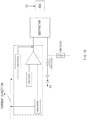
- FIG. 2 is a block diagram of a battery current measuring device 200 according to an embodiment of the present invention.
- the battery current measuring device 200 includes a switching element 201, a voltage measurement unit 202, a voltage amplification unit 204, an A/D converter 206, a temperature compensation unit 208, and a current calculation unit 210.
- the switching element 201 is formed in the charge/discharge path between the battery and the output terminal of the battery.
- the switching element 201 is controlled to be On/Off based on the control signal of the BMS, thereby supplying the power stored in the battery to the outside or charging the battery with external power.
- the switching element 201 may be, for example, a MOSFET, but is not limited thereto and any switching element may be applied as long as the switching element changes resistance depending on temperature.
- the voltage measurement unit 202 measures the voltage across the switching element 201.
- the voltage measurement unit 202 is configured to measure the voltage across the switching element 201 as an analog value, such as an analog front end.
- the voltage measurement unit 202 transmits the measured voltage signal across the switching element to the voltage amplification unit 204.
- the voltage across the switching element 201 may be amplified in the voltage amplification unit 204 without the voltage measurement unit 202.
- the voltage amplification unit 204 amplifies the voltage across the switching element applied directly from the switching element 201 or through the voltage measurement unit 202.
- the amplified voltage of the switching element 201 is transmitted to the A/D converter 206.
- the A/D converter 206 receives the amplified voltage signal of the switching element 201.
- the A/D converter 206 converts the receive voltage signal of the switching element 201 into a digital signal. That is, the A/D converter 206 converts the voltage across the switching element into a digital value.
- the A/D converter 206 uses a reference voltage that changes with temperature in converting the received voltage signal of the switching element 201 into a digital signal.
- the switching element 201 has a large change in resistance value with temperature. As the temperature of the switching element 201 is higher, the resistance becomes greater. Therefore, the switching element 201 is difficult to measure the correct voltage because the resistance is changed under the influence of the temperature change according to the heat generation of the battery.
- the temperature compensation unit 208 including a plurality of diodes is connected to a reference voltage input terminal of the A/D converter.
- the diode has a different voltage drop for a fixed current value as the temperature changes. Therefore, by using the diode type, number and connection configuration having a temperature-resistance curve similar to the resistance change curve with the temperature change of the switching element 201, it changes the reference voltage value of the A/D converter. As a result, it is possible to derive a more accurate voltage of the switching element 201 which is not affected by temperature.
- the reference voltage applied to the A/D converter for measuring the voltage across the switching element 201 is a voltage that is changed according to a temperature rather than a fixed voltage, for example, 5 V.
- Diodes which are semiconductor elements such as the switching element 201, have a forward voltage drop with temperature.
- the reference voltage changed through this diode compensates for the resistance change with temperature of the switching element 201.
- the diode is disposed on the same copper plate as the switching element 201 and is disposed close to the switching element 201.
- the temperature compensation unit 208 is connected to the A/D converter 206 to apply a reference voltage, and is configured to compensate for voltage values, which change with resistance changes due to temperature changes in the switching element 201. That is, the reference voltage is changed depending on the diode structure and the temperature.
- the temperature compensation unit 208 includes a diode structure in which a plurality of diodes are connected in series and in parallel. That is, the temperature compensation unit 208 includes a diode structure capable of compensating for the resistance change according to the temperature change of the switching element. One end of the temperature compensation unit 208 is connected to the power supply voltage, and the other end is connected to the A/D converter 206. That is, the diode structure is connected in series between the power supply voltage and the A/D converter 206 so that the reference voltage generated by the temperature compensation unit 208 is applied to the A/D converter 206.
- the diode is also a semiconductor device such as the switching element 201, the resistance value changes with temperature like the switching element 201.
- the type and number of diodes included in the diode structure and the connection configuration are adjusted to make the temperature-resistance curve the same.
- the accuracy of the measured voltage is determined by how similar the temperature-resistance curve of the switching element 201 and the temperature-resistance curve of the diode structure are.
- the diode structure may include a single diode, and in this case, the single diode is selected to have the same voltage drop characteristic to compensate for the voltage change with the temperature of the entire switching element 201.
- the temperature compensation unit is disposed close to the switching element.
- the A/D converter 206 receives the amplified measurement voltage of the switching element 201 received from the voltage amplification unit 204, converts the amplified voltage signal of the switching element 201 into a digital signal using the reference voltage determined by the temperature compensation unit 208, and transmits it to the current calculation unit 210.
- the current calculation unit 210 calculates the battery current using the digital signal received from the A/D converter 206, and calculates and computes battery information, such as the degeneration degree of the battery and the battery capacity, using the calculated battery current.
- FIG. 3 is a flowchart illustrating a battery current measuring method according to an embodiment of the present invention.
- a switching element that controls the charging and discharging of the battery for example, a MOSFET, is connected to the battery.
- MOSFETs are semiconductor devices and have a wide range of resistance changes with temperature.
- the voltage measurement unit 202 measures the voltage across the switching element 201 (S300).
- the voltage measurement unit 202 transmits the measured voltage signal across the switching element to the voltage amplification unit 204.
- the voltage across the switching element 201 may be amplified by the voltage amplification unit 204 immediately without the voltage measurement unit 202.
- the reference voltage of the A/D converter is changed.
- a diode structure is connected to the A/D converter.
- the diode structure may be composed of a single or a plurality of diodes. This will be described later.
- the voltage signal of the switching element 201 transmitted to the voltage amplification unit 204 is amplified by the voltage amplification unit (S302).
- the amplified voltage signal of the switching element 201 is transmitted to the A/D converter 206 (S304).
- the A/D converter 206 receiving the amplified voltage signal of the switching element 201 receives a reference voltage from the temperature compensation unit 208 (S306). That is, the reference voltage is set to compensate for the resistance change according to the temperature change of the switching element by the temperature compensation unit.
- the temperature compensation unit 208 includes a single or a plurality of diodes.
- the diode has a different voltage drop for a fixed current value as the temperature changes. Therefore, by using a diode having a temperature-resistance curve similar to the temperature-resistance curve with the change of temperature of the switching element 201 to change the reference voltage value of the A/D converter, the voltage of the switching element 201 can be derived to a more accurate voltage value that is not affected by temperature.
- the voltage drop of the input voltage is made according to the temperature by the diode included in the temperature compensation unit 208 so that the reference voltage transmitted to the A/D converter 206 may be changed according to the temperature.
- the reference voltage applied to the A/D converter for measuring the voltage across the switching element 201 is a reference voltage that is changed according to a temperature rather than a fixed voltage, for example, 5 V.
- Diodes which are semiconductors such as the switching element 201, have a forward voltage drop with temperature.
- the reference voltage changed through this diode compensates for the resistance change with temperature of the switching element 201.
- the diode is disposed on the same copper plate as the switching element 201 and is disposed close to the switching element 201.
- the temperature compensation unit 208 is connected to the A/D converter 206 to apply a reference voltage, and is configured to compensate for voltage values, which change with resistance changes due to temperature changes in the switching element 201.
- the A/D converter 206 converts the measured voltage signal of the switching element 201 into a digital signal by using the applied reference voltage (S308). That is, the amplified voltage is converted into a digital value by using the reference voltage set by the A/D converter.
- the A/D converter 206 transmits the converted digital signal to the current calculation unit 110 (S310).
- the current calculation unit 110 receiving the digital signal calculates the current of the switching element 201 using the received digital signal to estimate the battery current, and obtains battery information using the estimated battery current.
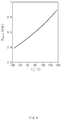
- FIG. 4 is a graph illustrating a change in resistance according to a temperature change of a MOSFET.
- the calculated current will change with temperature because the resistance of the MOSFET changes with temperature.
- the MOSFET is directly connected to the battery because it controls the charging/discharging of the battery, and the switching element 201 is also affected by the heat generated during a battery charging/discharging process. Therefore, it is difficult to accurately measure the voltage of the MOSFET as the resistance changes due to the heat of the MOSFET.
- the current will be a/(0.6 ⁇ 10-3)A
- the resistance when the temperature of MOSFET is 140 °C, since the resistance is 0.8 m ⁇ , the current will be a/(0.6 ⁇ 10-3)A. That is, since the resistance changes according to the temperature of the MOSFET, even if the measured voltage is the same, the resistance may vary depending on the temperature and thus the calculated current may be different.
- the present invention includes a separate temperature compensation unit to compensate for the voltage change according to the resistance change due to the heat of the MOSFET.
- FIG. 5 is a graph showing a change in current and voltage according to the temperature of a diode.
- the forward voltage drop of the diode varies according to the temperature when the same current flows. Referring to the graph of FIG. 5 , for example, if the current flows at 200 mA, a voltage drop of 100 mV is made at 150°C, a voltage drop of about 140 mV is made at 125°C, a voltage drop of about 190 mV is made at 100°C, and a voltage drop of about 230 mV is made at 75 °C.
- the reference voltage inputted to the A/D converter 206 is 4.9 V at 150°C, is about 4.86 V at 125°C, is about 4.81 V at 100°C, and is about 4.77 V at 75°C.
- such a diode By using the characteristics of such a diode, it can be implemented as a single diode using a diode having a temperature curve most similar to that of the MOSFET, and a plurality of diodes can also be connected in series to compensate for the changed voltage values at the MOSFETs.
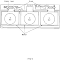
- FIG. 6 is an implementation example according to an embodiment of the present invention.
- the diode is disposed close to the MOSFET.
- the layer directly below the MOSFET layer, on which the MOSFET is disposed extends under the diode so that the MOSFET and the diode are located on the same layer.
- the diode is also selected as a device with the same voltage drop characteristics as the MOSFET, or connected in series to have the same temperature-resistance curve as the MOSFET. Accuracy is determined by how similar this temperature-resistance curve is.
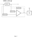
- FIG. 7 is an exemplary configuration diagram of a battery current measuring device using a conventional shunt resistor.
- a shunt resistor is connected in series between the battery and the output terminal, and the voltage across the shunt resistor is small so that it is amplified by the voltage amplification unit.
- the voltage amplified in the voltage amplification unit for example, an Op amp, is converted to a digital value through an analog to digital (A/D) converter.
- the reference voltage may be a fixed value, for example, 5 V.
- the digital signal converted by the A/D converter is transmitted to the MCU.
- the MCU receiving the digital signal it is converted to a current value again using the received digital signal.
- FIG. 8 is a configuration diagram of a battery current measuring device according to an embodiment of the present invention.
- Battery current is measured using a switching element that controls charging and discharging of the battery, for example, a MOSFET.
- the MOSFET is a semiconductor device, and it is difficult to measure the accurate voltage due to a large change in resistance with the change of temperature.
- the amplified signal After amplifying the voltage of the MOSFET through the OP amp, the amplified signal is converted into a digital signal in the A/D converter.
- the MOSFET is difficult to accurately measure the voltage due to the large width of the resistance change with the temperature change. Therefore, in order to compensate for this, the reference voltage of the A/D converter is changed.
- a diode structure is connected to the A/D converter.
- the diode structure may be composed of a single or a plurality of diodes.
- the diode connected to the A/D converter is selected to have the same voltage drop characteristic as the MOSFET, or a plurality of diodes are connected in series and in parallel to allow the temperature-resistance curve to be same as that of the MOSFET.
- the temperature-resistance curve is more similar to that of the MOSFET, the accuracy of the current measurement becomes higher.
- the digital signal converted by the A/D converter is transmitted to the MCU.
- the MCU receiving the digital signal from the A/D converter calculates the digital signal as a current again.
- Battery state information such as battery degeneration degree and capacity is calculated/computed by using the battery charge/discharge current converted in the MCU.
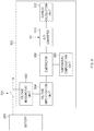
- FIG. 9 is a configuration diagram of a battery current measuring device according to another embodiment of the present invention.
- FIG. 9 The configuration of FIG. 9 is the same as that of FIG. 2 except for the configuration in which a subtractor 906 is added and the configuration in which a temperature compensation unit 908 is connected to the subtractor. Therefore, the description will be mainly focused on the configuration different from that of FIG. 2 .
- the voltage across the measured switching element 201 is amplified, and the amplified voltage signal is inputted to the first input terminal of the subtractor 906.
- the output voltage signal of the temperature compensation unit 908 is inputted to the second input terminal of the subtractor 906.
- the temperature compensation unit 908 is configured to compensate for the voltage value changed according to the resistance change caused by the temperature change of the switching element 201, and has the same temperature-resistance curve as the switching element 201.
- the output voltage signal of the temperature compensation unit 908 also changes with the temperature. Therefore, as a result, the difference between the voltage signals inputted to the first input terminal and the second input terminal of the subtractor 906 always remains constant. Accordingly, the output voltage signal of the subtractor 906 also remains constant regardless of the voltage change of the switching element 201 with temperature.
- the output voltage signal of the subtractor 906 is inputted to the A/D converter 910, and the A/D converter 910 converts the output voltage signal received from the subtractor 906 into a digital signal using the fixed reference voltage and transmits the converted digital signal to the current calculation unit 912.
- FIG. 10 is a configuration diagram of a battery current measuring device according to another embodiment of the present invention.
- FIG. 10 The configuration of FIG. 10 is the same as that of FIG. 8 except for the configuration in which a subtractor is added and the configuration in which a temperature compensation unit is connected to the subtractor. Therefore, the description will be mainly focused on the configuration different from that of FIG. 8 .
- the amplified signal After amplifying the measured MOSFET voltage through the OP amp, the amplified signal is inputted to the subtractor.
- the other input terminal of the subtractor is connected with a diode structure which is a temperature compensation unit.
- the diode structure connected to the subtractor includes a single or a plurality of diodes, and the diode structure has the same temperature-resistance curve as the MOSFET. Therefore, the difference between the output voltage signal of the diode structure inputted to the subtractor and the voltage across the MOSFET always remains constant, so that the output of the subtractor also remains constant.
- the voltage signal outputted from the subtractor is inputted to the A/D converter, and the A/D converter converts the voltage signal outputted from the subtractor into a digital signal using a fixed reference voltage.
- FIG. 11 is a flowchart illustrating a battery current measuring method according to another embodiment of the present invention.
- the voltage measurement unit 902 measures the voltage across the switching element 201 (S1100).
- the measured voltage signal at both ends of the switching element 201 is amplified by the voltage amplification unit 904 (S1110).
- the voltage across the switching element may be amplified by the voltage amplification unit 904 immediately without the voltage measurement unit 902.
- the voltage signal at both ends of the switching element 201 amplified by the voltage amplification unit 904 is received at the first input terminal of the subtractor (SI120).
- the temperature compensation unit 908 is configured to compensate for the voltage value changed according to the resistance change caused by the temperature change of the switching element 201, and has the same temperature-resistance curve as the switching element 201.
- the output voltage signal of the temperature compensation unit 908 also changes with the temperature.
- the difference between the both signals inputted to the subtractor always remains constant. Accordingly, even though the voltage of the switching element 201 changes with temperature, the output voltage signal of the subtractor 906 also remains constant.
- the output voltage signal of the subtractor 906 is inputted to the A/D converter 910 (SI140).
- the A/D converter 910 converts the inputted output voltage signal of the subtractor 906 into a digital signal using a fixed reference voltage, for example, 5 V (S1150), and transmits the digital signal to the MCU (S1160).
Landscapes
- Physics & Mathematics (AREA)
- General Physics & Mathematics (AREA)
- Engineering & Computer Science (AREA)
- Power Engineering (AREA)
- Measurement Of Current Or Voltage (AREA)
- Secondary Cells (AREA)
Abstract
Description
- This application claims priority to and the benefit of
Korean Patent Application No. 10-2019-0001151, filed on January 4, 2019 - The present invention relates to a battery current measuring device and method. In particular, the present invention relates to a device and method for measuring battery current without using a shunt resistor.
- The charge/discharge current of the battery must be measured to calculate/compute not only the output but also battery information such as battery degeneration information and battery capacity. In addition, precise measurement accuracy is required in order to accurately calculate the battery information, and in order to meet this, conventionally, a battery current is measured using a precision resistor such as a shunt.
- However, since these shunt resistors also occupy a large volume and add cost, assembly processes, and the like, a better solution is required.
- As a means for measuring the current of the battery, an object of the present invention is to obtain an efficient battery current measuring means without using a shunt resistor that occupies a large volume and adds cost and assembly process.
- A battery current measuring device according to an embodiment of the present invention includes: a switching element configured to control charging and discharging of a battery: an A/D converter configured to convert a voltage value across the switching element into a digital value; a temperature compensation unit having a diode structure capable of compensating for a resistance change according to a change of temperature of the switching element; and a current calculation unit configured to calculate a current flowing through the switching element based on the digital value of the voltage value, and the A/D converter converts the voltage value of the switching element into the digital value using a reference voltage inputted from the temperature compensation unit.
- According to one feature of this embodiment, the diode structure of the temperature compensation unit includes a plurality of diodes, and a number and connection configuration of the plurality of diodes are determined so as to have a temperature-resistance curve matching a temperature-resistance curve of the switching element.
- According to another feature of this embodiment, the battery current measuring device further includes a voltage amplification unit configured to amplify the voltage value before applying the voltage value across the switching element to the A/D converter.
- According to another feature of this embodiment, the reference voltage is changed according to the diode structure and the temperature.
- According to another feature of this embodiment, the temperature compensation unit is disposed close to the switching element.
- According to another feature of this embodiment, the switching element is a MOSFET.
- According to another feature of this embodiment, the temperature compensation unit is formed on a same layer as a layer on which the MOSFET is formed on a substrate on which the battery current measuring device is installed.
- A battery current measuring method according to an embodiment of the present invention includes: receiving a voltage across a switching element for controlling charging and discharging of a battery; generating a reference voltage for compensating for a resistance change according to a temperature change of the switching element; converting the voltage of the switching element into a digital value using the generated reference voltage; and calculating a current flowing through the switching element based on the digital value.
- A battery pack according to an embodiment of the present invention includes: a battery capable of being charged and discharged; a switching element configured to control charging and discharging of the battery: an A/D converter configured to convert a voltage value across the switching element into a digital value; a temperature compensation unit having a diode structure capable of compensating for a resistance change according to a temperature change of the switching element; and a current calculation unit configured to calculate a current flowing through the switching element based on the digital value of the voltage value, and the A/D converter converts the voltage value of the switching element into the digital value using a reference voltage inputted from the temperature compensation unit.
- A battery current measuring device according to an embodiment of the present invention includes: a switching element configured to control charging and discharging of a battery: an A/D converter configured to convert a voltage across the switching element into a digital value; a temperature compensation unit including a diode structure that has a temperature-resistance curve matching the switching element and is capable of compensating for a resistance change according to a temperature change of the switching element; a subtractor configured to receive the voltage across the switching element and an output of the temperature compensation unit and output a constant voltage signal; and a current calculation unit configured to calculate a current flowing through the switching element based on the digital value of the voltage, and the A/D converter converts the voltage signal inputted from the subtractor into the digital value using a fixed reference voltage.
- The present invention is to measure the current of the battery using a semiconductor switch to turn on/off the battery without using a shunt resistor so that the volume can be reduced and it is more efficient in terms of cost and production process.
-
-
FIG. 1 is a view briefly comparing a conventional battery current measuring device with a battery current measuring device according to an embodiment of the present invention. -
FIG. 2 is a block diagram of a battery current measuring device according to an embodiment of the present invention. -
FIG. 3 is a flowchart illustrating a battery current measuring method according to an embodiment of the present invention. -
FIG. 4 is a graph illustrating a change in resistance according to a temperature change of a MOSFET. -
FIG. 5 is a graph showing a change in current and voltage according to the temperature of a diode. -
FIG. 6 is an implementation example according to an embodiment of the present invention. -
FIG. 7 is an exemplary configuration diagram of a battery current measuring device using a conventional shunt resistor. -
FIG. 8 is a configuration diagram of a battery current measuring device according to an embodiment of the present invention. -
FIG. 9 is a configuration diagram of a battery current measuring device according to another embodiment of the present invention. -
FIG. 10 is a configuration diagram of a battery current measuring device according to another embodiment of the present invention. -
FIG. 11 is a flowchart illustrating a battery current measuring method according to another embodiment of the present invention. - Hereinafter, some embodiments of the present invention will be described in detail through exemplary drawings. It should be noted that, in assigning reference numerals to components of each drawing, although the components are displayed on different drawings, like reference numerals refer to like components. Additionally, in describing the inventive concept, detailed descriptions of well-known configurations or functions will be omitted if it is determined that they would obscure the subject matter of the inventive concept.
- In order to solve the problem of the above-mentioned shunt resistor, the present invention includes a method and device that can measure current using essential components of the battery to measure the current of the battery without using a shunt resistor.
- In general, a switching element for controlling charging and discharging by turning on/off a battery must be essentially present, and the switching element is composed of a semiconductor device such as a MOSFET.
- Since the resistance of semiconductor devices such as MOSFETs is generally similar to shunt resistors, although there is the method of measuring the current through the conventional method, semiconductors have not been used to measure practically accurate currents because of the large magnitude of change in resistance with temperature.
- However, the present invention includes the diode configuration as described below, thereby making it possible to accurately measure the current of the battery by supplementing the difficulty of accurate current measurement according to the resistance change of the MOSFET with temperature. Hereinafter, the configuration of the present invention will be described in more detail.
- Here, the type of battery is not particularly limited, and for example, the battery may be composed of a lithium ion battery, a lithium polymer battery, a nickel cadmium battery, a nickel hydrogen battery, a nickel zinc battery, and the like.
- In addition, a plurality of battery cells are formed of a battery module connected in series and/or parallel, and at least one battery module is combined with a Battery Management System (BMS) to form a battery pack.
- The BMS estimates the state of the battery and manages the battery using the estimated state information.
- Hereinafter, the battery cell or battery module will be referred to simply as a battery.
-
FIG. 1 is a view briefly comparing a conventional battery current measuring device with a battery current measuring device according to an embodiment of the present invention. - In
FIG. 1 , the view on the left side is a simplified diagram of a battery current measuring device for measuring current of a battery using a conventional shunt resistor. - In order to measure the battery current, a shunt resistor is connected in series on one side of the battery, and the BMS calculates the battery current by measuring the voltage across the connected shunt resistor. Hereinafter, the battery current measuring method through the shunt resistor will be described in more detail.
- A shunt resistor is connected in series on one side of the battery and the voltage across the shunt resistor is measured by a voltage measurement unit. The voltage across the shunt resistor is amplified by the voltage amplification unit because of its small size.
- The voltage amplified by the voltage amplification unit is converted to a digital value through an analog to digital (A/D) converter. In this case, the reference voltage of the A/D converter may be a fixed value, for example, 5 V.
- The digital signal converted by the A/D converter is transmitted to the MCU. In the MCU receiving the digital signal, the current of the battery is calculated using the received digital signal.
- Here, the voltage measurement unit, the voltage amplification unit, the A/D converter, and the MCU are included in the Battery Management System (BMS).
- In addition to the shunt resistor, a switching element for controlling charging and discharging of the battery is located on the current path between the battery and the output terminal. The switching element is generally a semiconductor device, preferably a MOSFET. The switching element receives the control signal from the BMS to perform charging and discharging of the battery.
- In
FIG. 1 , the view on the right side is a simplified diagram of a battery current measuring device according to an embodiment of the present invention. - The battery current measuring device according to an embodiment of the present invention does not include a shunt resistor unlike a conventional battery current measuring device.
- However, a battery current is calculated by using a switching element, for example, a MOSFET, for controlling charging and discharging of the battery.
- That is, in embodiments of the present invention, the voltage across the MOSFET is measured by the voltage measurement unit. However, MOSFETs are semiconductor devices, and the resistance changes greatly with the change in temperature. The MOSFET is directly connected to the battery because it performs charging/discharging control of the battery, and because of the heat generated during battery charging/discharging, MOSFETs are also affected by battery heat. Therefore, it is difficult to accurately measure the voltage of the MOSFET as the resistance changes due to the heat of the MOSFET.
- Therefore, the present invention includes a separate temperature compensation unit to compensate for the resistance change caused by the heat of the MOSFET. This will be described later.
- The voltage measured across the MOSFET is amplified by the voltage amplification unit. The amplified signal is converted into a digital signal by the A/D converter. That is, the A/D converter converts the voltage across the switching element into a digital value.
- However, as described above, in order to compensate for the resistance change caused by the temperature change of the MOSFET, the reference voltage of the A/D converter is changed. In order to change the reference voltage of the A/D converter, a diode structure is connected to the A/D converter. The diode structure may be composed of a single or a plurality of diodes.
- In addition, since the resistance may vary depending on the type and number of MOSFET devices and their connection configurations, the diode connected to the A/D converter is selected to have the same voltage drop characteristic as the MOSFET, or a plurality of diodes are connected in series and in parallel to allow the temperature curve to be the same as that of the MOSFET. That is, the plurality of diodes have a temperature-resistance curve that matches the temperature-resistance curve of the MOSFET which is the switching element. Here, as the temperature curve is more similar to that of the MOSFET, the accuracy of the current measurement becomes higher.
- For more accurate measurements with the same temperature curve as the MOSFET, a plurality of diodes connected to the A/D converter are placed on the same copper plate as the MOSFET and placed close to the MOSFET to create an environment with a temperature that is identical to a temperature that affects the MOSFET.
- The digital signal converted by the A/D converter is transmitted to the MCU which is a current calculation unit. The MCU receiving the digital signal from the A/D converter converts the digital signal to the current flowing through the switching element again. The charge/discharge current of the battery can be calculated from the current flowing through the switching element. Battery state information such as battery degeneration degree and capacity is calculated/computed by using the battery charge/discharge current converted in the MCU.
-
FIG. 2 is a block diagram of a batterycurrent measuring device 200 according to an embodiment of the present invention. - The battery
current measuring device 200 includes aswitching element 201, avoltage measurement unit 202, avoltage amplification unit 204, an A/D converter 206, a temperature compensation unit 208, and acurrent calculation unit 210. - The switching
element 201 is formed in the charge/discharge path between the battery and the output terminal of the battery. The switchingelement 201 is controlled to be On/Off based on the control signal of the BMS, thereby supplying the power stored in the battery to the outside or charging the battery with external power. In the embodiments of the present invention, the switchingelement 201 may be, for example, a MOSFET, but is not limited thereto and any switching element may be applied as long as the switching element changes resistance depending on temperature. - The
voltage measurement unit 202 measures the voltage across the switchingelement 201. Here, thevoltage measurement unit 202 is configured to measure the voltage across the switchingelement 201 as an analog value, such as an analog front end. Thevoltage measurement unit 202 transmits the measured voltage signal across the switching element to thevoltage amplification unit 204. The voltage across the switchingelement 201 may be amplified in thevoltage amplification unit 204 without thevoltage measurement unit 202. - The
voltage amplification unit 204 amplifies the voltage across the switching element applied directly from the switchingelement 201 or through thevoltage measurement unit 202. The amplified voltage of theswitching element 201 is transmitted to the A/D converter 206. - The A/
D converter 206 receives the amplified voltage signal of theswitching element 201. The A/D converter 206 converts the receive voltage signal of theswitching element 201 into a digital signal. That is, the A/D converter 206 converts the voltage across the switching element into a digital value. The A/D converter 206 uses a reference voltage that changes with temperature in converting the received voltage signal of theswitching element 201 into a digital signal. - Specifically, the switching
element 201 has a large change in resistance value with temperature. As the temperature of theswitching element 201 is higher, the resistance becomes greater. Therefore, the switchingelement 201 is difficult to measure the correct voltage because the resistance is changed under the influence of the temperature change according to the heat generation of the battery. In order to supplement the characteristics of theswitching element 201 and derive an accurate voltage value, the temperature compensation unit 208 including a plurality of diodes is connected to a reference voltage input terminal of the A/D converter. - The diode has a different voltage drop for a fixed current value as the temperature changes. Therefore, by using the diode type, number and connection configuration having a temperature-resistance curve similar to the resistance change curve with the temperature change of the
switching element 201, it changes the reference voltage value of the A/D converter. As a result, it is possible to derive a more accurate voltage of theswitching element 201 which is not affected by temperature. - That is, according to the present invention, the reference voltage applied to the A/D converter for measuring the voltage across the switching
element 201 is a voltage that is changed according to a temperature rather than a fixed voltage, for example, 5 V. Diodes, which are semiconductor elements such as the switchingelement 201, have a forward voltage drop with temperature. Thus, the reference voltage changed through this diode compensates for the resistance change with temperature of theswitching element 201. - At this time, in order to allow the diode to operate in the environment of the same temperature as the switching
element 201, the diode is disposed on the same copper plate as the switchingelement 201 and is disposed close to theswitching element 201. - As described above, the temperature compensation unit 208 is connected to the A/
D converter 206 to apply a reference voltage, and is configured to compensate for voltage values, which change with resistance changes due to temperature changes in theswitching element 201. That is, the reference voltage is changed depending on the diode structure and the temperature. - Specifically, the temperature compensation unit 208 includes a diode structure in which a plurality of diodes are connected in series and in parallel. That is, the temperature compensation unit 208 includes a diode structure capable of compensating for the resistance change according to the temperature change of the switching element. One end of the temperature compensation unit 208 is connected to the power supply voltage, and the other end is connected to the A/
D converter 206. That is, the diode structure is connected in series between the power supply voltage and the A/D converter 206 so that the reference voltage generated by the temperature compensation unit 208 is applied to the A/D converter 206. - Since the diode is also a semiconductor device such as the switching
element 201, the resistance value changes with temperature like theswitching element 201. In addition, since the resistance varies depending on the type of theswitching element 201, the type and number of diodes included in the diode structure and the connection configuration are adjusted to make the temperature-resistance curve the same. At this time, the accuracy of the measured voltage is determined by how similar the temperature-resistance curve of theswitching element 201 and the temperature-resistance curve of the diode structure are. Meanwhile, the diode structure may include a single diode, and in this case, the single diode is selected to have the same voltage drop characteristic to compensate for the voltage change with the temperature of theentire switching element 201. Furthermore, the temperature compensation unit is disposed close to the switching element. - The A/
D converter 206 receives the amplified measurement voltage of theswitching element 201 received from thevoltage amplification unit 204, converts the amplified voltage signal of theswitching element 201 into a digital signal using the reference voltage determined by the temperature compensation unit 208, and transmits it to thecurrent calculation unit 210. - The
current calculation unit 210 calculates the battery current using the digital signal received from the A/D converter 206, and calculates and computes battery information, such as the degeneration degree of the battery and the battery capacity, using the calculated battery current. -
FIG. 3 is a flowchart illustrating a battery current measuring method according to an embodiment of the present invention. - A switching element that controls the charging and discharging of the battery, for example, a MOSFET, is connected to the battery. MOSFETs are semiconductor devices and have a wide range of resistance changes with temperature. The
voltage measurement unit 202 measures the voltage across the switching element 201 (S300). Thevoltage measurement unit 202 transmits the measured voltage signal across the switching element to thevoltage amplification unit 204. The voltage across the switchingelement 201 may be amplified by thevoltage amplification unit 204 immediately without thevoltage measurement unit 202. - Here, in relation to the measured voltage, in order to compensate for the resistance change due to the temperature change of the switching element, the reference voltage of the A/D converter is changed. In order to change the reference voltage of the A/D converter, a diode structure is connected to the A/D converter. The diode structure may be composed of a single or a plurality of diodes. This will be described later.
- The voltage signal of the
switching element 201 transmitted to thevoltage amplification unit 204 is amplified by the voltage amplification unit (S302). The amplified voltage signal of theswitching element 201 is transmitted to the A/D converter 206 (S304). - The A/
D converter 206 receiving the amplified voltage signal of theswitching element 201 receives a reference voltage from the temperature compensation unit 208 (S306). That is, the reference voltage is set to compensate for the resistance change according to the temperature change of the switching element by the temperature compensation unit. - Specifically, the temperature compensation unit 208 includes a single or a plurality of diodes. The diode has a different voltage drop for a fixed current value as the temperature changes. Therefore, by using a diode having a temperature-resistance curve similar to the temperature-resistance curve with the change of temperature of the
switching element 201 to change the reference voltage value of the A/D converter, the voltage of theswitching element 201 can be derived to a more accurate voltage value that is not affected by temperature. - The voltage drop of the input voltage is made according to the temperature by the diode included in the temperature compensation unit 208 so that the reference voltage transmitted to the A/
D converter 206 may be changed according to the temperature. - That is, according to the present invention, the reference voltage applied to the A/D converter for measuring the voltage across the switching
element 201 is a reference voltage that is changed according to a temperature rather than a fixed voltage, for example, 5 V. Diodes, which are semiconductors such as the switchingelement 201, have a forward voltage drop with temperature. Thus, the reference voltage changed through this diode compensates for the resistance change with temperature of theswitching element 201. - At this time, in order to allow the diode to operate in the environment of the same temperature as the switching
element 201, the diode is disposed on the same copper plate as the switchingelement 201 and is disposed close to theswitching element 201. - As described above, the temperature compensation unit 208 is connected to the A/
D converter 206 to apply a reference voltage, and is configured to compensate for voltage values, which change with resistance changes due to temperature changes in theswitching element 201. - The A/
D converter 206 converts the measured voltage signal of theswitching element 201 into a digital signal by using the applied reference voltage (S308). That is, the amplified voltage is converted into a digital value by using the reference voltage set by the A/D converter. - The A/
D converter 206 transmits the converted digital signal to the current calculation unit 110 (S310). - The current calculation unit 110 receiving the digital signal calculates the current of the
switching element 201 using the received digital signal to estimate the battery current, and obtains battery information using the estimated battery current. -
FIG. 4 is a graph illustrating a change in resistance according to a temperature change of a MOSFET. - As the MOSFET has a resistance change with temperature as in the graph shown in
FIG. 4 , due to the changing resistance of the MOSFET, the current cannot be calculated accurately through V=I∗R. - That is, even if the voltage across the MOSFET is measured equally, the calculated current will change with temperature because the resistance of the MOSFET changes with temperature. The MOSFET is directly connected to the battery because it controls the charging/discharging of the battery, and the
switching element 201 is also affected by the heat generated during a battery charging/discharging process. Therefore, it is difficult to accurately measure the voltage of the MOSFET as the resistance changes due to the heat of the MOSFET. - For example, even if the measured voltage across the MOSFET is a V, since the resistance is 0.6 mΩ when the temperature of the MOSFET is 60 °C, the current will be a/(0.6∗10-3)A, and when the temperature of MOSFET is 140 °C, since the resistance is 0.8 mΩ , the current will be a/(0.6∗10-3)A. That is, since the resistance changes according to the temperature of the MOSFET, even if the measured voltage is the same, the resistance may vary depending on the temperature and thus the calculated current may be different.
- In order to compensate for this, the present invention includes a separate temperature compensation unit to compensate for the voltage change according to the resistance change due to the heat of the MOSFET.
-
FIG. 5 is a graph showing a change in current and voltage according to the temperature of a diode. - The forward voltage drop of the diode varies according to the temperature when the same current flows. Referring to the graph of
FIG. 5 , for example, if the current flows at 200 mA, a voltage drop of 100 mV is made at 150°C, a voltage drop of about 140 mV is made at 125°C, a voltage drop of about 190 mV is made at 100°C, and a voltage drop of about 230 mV is made at 75 °C. - Thus, for example, if the input voltage of the diode structure is 5 V, by forward voltage drop of the diode, the reference voltage inputted to the A/
D converter 206 is 4.9 V at 150°C, is about 4.86 V at 125°C, is about 4.81 V at 100°C, and is about 4.77 V at 75°C. - By using the characteristics of such a diode, it can be implemented as a single diode using a diode having a temperature curve most similar to that of the MOSFET, and a plurality of diodes can also be connected in series to compensate for the changed voltage values at the MOSFETs.
-
FIG. 6 is an implementation example according to an embodiment of the present invention. - As shown in
FIG. 6 , the diode is disposed close to the MOSFET. In addition, the layer directly below the MOSFET layer, on which the MOSFET is disposed, extends under the diode so that the MOSFET and the diode are located on the same layer. - This is to reduce the temperature deviation by allowing the MOSFET and the diode to be disposed on the same layer.
- In addition, since the resistance varies depending on the MOSFET device type and the number of parallels, the diode is also selected as a device with the same voltage drop characteristics as the MOSFET, or connected in series to have the same temperature-resistance curve as the MOSFET. Accuracy is determined by how similar this temperature-resistance curve is.
-
FIG. 7 is an exemplary configuration diagram of a battery current measuring device using a conventional shunt resistor. - A shunt resistor is connected in series between the battery and the output terminal, and the voltage across the shunt resistor is small so that it is amplified by the voltage amplification unit.
- The voltage amplified in the voltage amplification unit, for example, an Op amp, is converted to a digital value through an analog to digital (A/D) converter. In this case, the reference voltage may be a fixed value, for example, 5 V.
- The digital signal converted by the A/D converter is transmitted to the MCU. In the MCU receiving the digital signal, it is converted to a current value again using the received digital signal.
-
FIG. 8 is a configuration diagram of a battery current measuring device according to an embodiment of the present invention. - Battery current is measured using a switching element that controls charging and discharging of the battery, for example, a MOSFET. The MOSFET is a semiconductor device, and it is difficult to measure the accurate voltage due to a large change in resistance with the change of temperature.
- After amplifying the voltage of the MOSFET through the OP amp, the amplified signal is converted into a digital signal in the A/D converter.
- However, as described above, the MOSFET is difficult to accurately measure the voltage due to the large width of the resistance change with the temperature change. Therefore, in order to compensate for this, the reference voltage of the A/D converter is changed. In order to change the reference voltage of the A/D converter, a diode structure is connected to the A/D converter. The diode structure may be composed of a single or a plurality of diodes.
- In addition, since the resistance may vary depending on the type and number of MOSFET devices and their connection configurations, the diode connected to the A/D converter is selected to have the same voltage drop characteristic as the MOSFET, or a plurality of diodes are connected in series and in parallel to allow the temperature-resistance curve to be same as that of the MOSFET. Here, as the temperature-resistance curve is more similar to that of the MOSFET, the accuracy of the current measurement becomes higher.
- The digital signal converted by the A/D converter is transmitted to the MCU. The MCU receiving the digital signal from the A/D converter calculates the digital signal as a current again. Battery state information such as battery degeneration degree and capacity is calculated/computed by using the battery charge/discharge current converted in the MCU.
-
FIG. 9 is a configuration diagram of a battery current measuring device according to another embodiment of the present invention. - The configuration of
FIG. 9 is the same as that ofFIG. 2 except for the configuration in which asubtractor 906 is added and the configuration in which atemperature compensation unit 908 is connected to the subtractor. Therefore, the description will be mainly focused on the configuration different from that ofFIG. 2 . - The voltage across the measured switching
element 201 is amplified, and the amplified voltage signal is inputted to the first input terminal of thesubtractor 906. In addition, the output voltage signal of thetemperature compensation unit 908 is inputted to the second input terminal of thesubtractor 906. - Here, the
temperature compensation unit 908 is configured to compensate for the voltage value changed according to the resistance change caused by the temperature change of theswitching element 201, and has the same temperature-resistance curve as the switchingelement 201. Thus, like the output voltage signal of thevoltage amplification unit 904 that changes with the temperature of theswitching element 201, the output voltage signal of thetemperature compensation unit 908 also changes with the temperature. Therefore, as a result, the difference between the voltage signals inputted to the first input terminal and the second input terminal of thesubtractor 906 always remains constant. Accordingly, the output voltage signal of thesubtractor 906 also remains constant regardless of the voltage change of theswitching element 201 with temperature. - The output voltage signal of the
subtractor 906 is inputted to the A/D converter 910, and the A/D converter 910 converts the output voltage signal received from thesubtractor 906 into a digital signal using the fixed reference voltage and transmits the converted digital signal to thecurrent calculation unit 912. -
FIG. 10 is a configuration diagram of a battery current measuring device according to another embodiment of the present invention. - The configuration of
FIG. 10 is the same as that ofFIG. 8 except for the configuration in which a subtractor is added and the configuration in which a temperature compensation unit is connected to the subtractor. Therefore, the description will be mainly focused on the configuration different from that ofFIG. 8 . - After amplifying the measured MOSFET voltage through the OP amp, the amplified signal is inputted to the subtractor. However, since the MOSFET has a large change in resistance due to temperature change, in order to compensate for this, the other input terminal of the subtractor is connected with a diode structure which is a temperature compensation unit.
- The diode structure connected to the subtractor includes a single or a plurality of diodes, and the diode structure has the same temperature-resistance curve as the MOSFET. Therefore, the difference between the output voltage signal of the diode structure inputted to the subtractor and the voltage across the MOSFET always remains constant, so that the output of the subtractor also remains constant.
- The voltage signal outputted from the subtractor is inputted to the A/D converter, and the A/D converter converts the voltage signal outputted from the subtractor into a digital signal using a fixed reference voltage.
-
FIG. 11 is a flowchart illustrating a battery current measuring method according to another embodiment of the present invention. - The
voltage measurement unit 902 measures the voltage across the switching element 201 (S1100). - The measured voltage signal at both ends of the
switching element 201 is amplified by the voltage amplification unit 904 (S1110). Here, the voltage across the switching element may be amplified by thevoltage amplification unit 904 immediately without thevoltage measurement unit 902. - The voltage signal at both ends of the
switching element 201 amplified by thevoltage amplification unit 904 is received at the first input terminal of the subtractor (SI120). - Meanwhile, the output voltage signal of the
temperature compensation unit 908 connected to the other input terminal of thesubtractor 906 is inputted to the second input terminal of the subtractor 906 (S1130). - As described above, the
temperature compensation unit 908 is configured to compensate for the voltage value changed according to the resistance change caused by the temperature change of theswitching element 201, and has the same temperature-resistance curve as the switchingelement 201. Thus, like the output voltage signal of thevoltage amplification unit 904 that changes with the temperature of theswitching element 201, the output voltage signal of thetemperature compensation unit 908 also changes with the temperature. - Therefore, the difference between the both signals inputted to the subtractor always remains constant. Accordingly, even though the voltage of the
switching element 201 changes with temperature, the output voltage signal of thesubtractor 906 also remains constant. - The output voltage signal of the
subtractor 906 is inputted to the A/D converter 910 (SI140). - The A/
D converter 910 converts the inputted output voltage signal of thesubtractor 906 into a digital signal using a fixed reference voltage, for example, 5 V (S1150), and transmits the digital signal to the MCU (S1160). - Although the present invention has been described above by limited embodiments and drawings, the present invention is not limited thereto, and it will be apparent to those skilled in the art that the present invention may be implemented in various ways within the equivalent scope of the technical spirit of the present invention and the claims to be described below.
Claims (12)
- A battery current measuring device comprising:a switching element configured to control charging and discharging of a battery:an A/D converter configured to convert a voltage value across the switching element into a digital value;a temperature compensation unit having a diode structure capable of compensating for a resistance change according to a change of temperature of the switching element; anda current calculation unit configured to calculate a current flowing through the switching element based on the digital value of the voltage value,wherein the A/D converter converts the voltage value of the switching element into the digital value using a reference voltage inputted from the temperature compensation unit.
- The battery current measuring device of claim 1, wherein the diode structure of the temperature compensation unit comprises a plurality of diodes,
wherein a number and connection configuration of the plurality of diodes are determined so as to have a temperature-resistance curve matching a temperature-resistance curve of the switching element. - The battery current measuring device of claim 2, further comprising a voltage amplification unit configured to amplify the voltage value before applying the voltage value across the switching element to the A/D converter.
- The battery current measuring device of claim 2, wherein the reference voltage is changed according to the diode structure and the temperature.
- The battery current measuring device of claim 1, wherein the temperature compensation unit is disposed close to the switching element.
- The battery current measuring device of claim 1, wherein the switching element is a MOSFET.
- The battery current measuring device of claim 6, wherein the temperature compensation unit is formed on a same layer as a layer on which the MOSFET is formed on a substrate on which the battery current measuring device is installed.
- A battery current measuring method comprising:receiving a voltage across a switching element for controlling charging and discharging of a battery;generating a reference voltage for compensating for a resistance change according to a temperature change of the switching element;converting the voltage of the switching element into a digital value using the generated reference voltage; andcalculating a current flowing through the switching element based on the digital value.
- The battery current measuring method of claim 8, wherein the reference voltage is generated by a diode structure including a plurality of diodes,
wherein a number and connection configuration of the plurality of diodes are determined so as to have a temperature-resistance curve matching a temperature-resistance curve of the switching element. - The battery current measuring method of claim 8, wherein the diode structure is disposed close to the switching element.
- A battery pack comprising:a battery capable of being charged and discharged;a switching element configured to control charging and discharging of the battery:an A/D converter configured to convert a voltage value across the switching element into a digital value;a temperature compensation unit having a diode structure capable of compensating for a resistance change according to a temperature change of the switching element; anda current calculation unit configured to calculate a current flowing through the switching element based on the digital value of the voltage value,wherein the A/D converter converts the voltage value of the switching element into the digital value using a reference voltage inputted from the temperature compensation unit.
- A battery current measuring device comprising:a switching element configured to control charging and discharging of a battery:an A/D converter configured to convert a voltage across the switching element into a digital value;a temperature compensation unit including a diode structure that has a temperature-resistance curve matching the switching element and is capable of compensating for a resistance change according to a temperature change of the switching element;a subtractor configured to receive the voltage across the switching element and an output of the temperature compensation unit and output a constant voltage signal; anda current calculation unit configured to calculate a current flowing through the switching element based on the digital value of the voltage,wherein the A/D converter converts the voltage signal inputted from the subtractor into the digital value using a fixed reference voltage.
Applications Claiming Priority (2)
| Application Number | Priority Date | Filing Date | Title |
|---|---|---|---|
| KR1020190001151A KR102754587B1 (en) | 2019-01-04 | 2019-01-04 | Apparatus and Method for measuring current of battery |
| PCT/KR2020/000140 WO2020141944A1 (en) | 2019-01-04 | 2020-01-03 | Battery current measuring device and method |
Publications (3)
| Publication Number | Publication Date |
|---|---|
| EP3889625A1 true EP3889625A1 (en) | 2021-10-06 |
| EP3889625A4 EP3889625A4 (en) | 2022-01-12 |
| EP3889625B1 EP3889625B1 (en) | 2024-10-30 |
Family
ID=71407065
Family Applications (1)
| Application Number | Title | Priority Date | Filing Date |
|---|---|---|---|
| EP20736203.9A Active EP3889625B1 (en) | 2019-01-04 | 2020-01-03 | Battery current measuring device and method |
Country Status (8)
| Country | Link |
|---|---|
| US (1) | US11835585B2 (en) |
| EP (1) | EP3889625B1 (en) |
| JP (1) | JP7364156B2 (en) |
| KR (1) | KR102754587B1 (en) |
| CN (1) | CN113678008B (en) |
| ES (1) | ES2998809T3 (en) |
| HU (1) | HUE068974T2 (en) |
| WO (1) | WO2020141944A1 (en) |
Families Citing this family (7)
| Publication number | Priority date | Publication date | Assignee | Title |
|---|---|---|---|---|
| WO2021152511A1 (en) * | 2020-01-31 | 2021-08-05 | Briggs & Stratton, Llc | Serviceable battery pack |
| KR102460421B1 (en) * | 2020-12-04 | 2022-10-31 | 현대모비스 주식회사 | Apparatus and method for monitoring current of power semiconductor device |
| CN115420996A (en) * | 2022-08-15 | 2022-12-02 | 广州科技贸易职业学院 | Current sampling device and method for aviation high-voltage direct-current power distribution system |
| KR102830821B1 (en) * | 2022-09-23 | 2025-07-07 | 주식회사 원익피앤이 | Current sensing circuit for charge/discharge probe and charger/discharger comprising the same |
| CN116593764B (en) * | 2023-03-29 | 2024-06-25 | 浙江朗德电子科技有限公司 | High-precision self-calibration current sensor module and calibration method thereof |
| CN118151714B (en) * | 2024-02-26 | 2024-09-10 | 北京炎黄国芯科技有限公司 | Charging and discharging digital-analog mixed voltage compensation method |
| CN119246925B (en) * | 2024-06-03 | 2025-09-19 | 华润微集成电路(无锡)有限公司 | Voltage measurement temperature effect calibration circuit and method, battery management system and vehicle |
Family Cites Families (34)
| Publication number | Priority date | Publication date | Assignee | Title |
|---|---|---|---|---|
| JPH03180784A (en) * | 1989-12-11 | 1991-08-06 | Canon Inc | Calculator for residual capacity of battery |
| JPH03296667A (en) * | 1990-04-03 | 1991-12-27 | Motorola Inc | Temperature-compensated power detector |
| JPH06188641A (en) | 1992-12-17 | 1994-07-08 | Fuji Electric Co Ltd | Current detector and current limiter |
| DE19745040C2 (en) | 1997-02-10 | 2003-03-27 | Daimler Chrysler Ag | Arrangement and method for measuring a temperature |
| JP2000299631A (en) * | 1999-04-12 | 2000-10-24 | Yazaki Corp | Power supply control device and power supply control method |
| JP4136237B2 (en) | 1999-12-08 | 2008-08-20 | 富士電機機器制御株式会社 | Gate threshold temperature compensation circuit for MOSFET for switching power supply |
| JP4612174B2 (en) * | 2000-11-10 | 2011-01-12 | 株式会社東芝 | Battery current measurement circuit |
| US6812677B2 (en) | 2001-08-21 | 2004-11-02 | Intersil Americas Inc. | Thermally compensated current sensing of intrinsic power converter elements |
| JP4872176B2 (en) * | 2001-08-29 | 2012-02-08 | 株式会社デンソー | Junction FET drive circuit |
| JP4236402B2 (en) | 2001-10-09 | 2009-03-11 | 富士通マイクロエレクトロニクス株式会社 | Semiconductor device |
| DE10237920B3 (en) * | 2002-08-14 | 2004-02-19 | Siemens Ag | Current measuring method with compression of measured analogue signal before A/D conversion and transmission from high potential measuring point to earth point |
| JP4062301B2 (en) * | 2004-11-19 | 2008-03-19 | 株式会社デンソー | Vehicle power supply |
| US7339230B2 (en) | 2006-01-09 | 2008-03-04 | International Business Machines Corporation | Structure and method for making high density mosfet circuits with different height contact lines |
| JP4434214B2 (en) * | 2007-02-08 | 2010-03-17 | 株式会社デンソー | Battery state detection device |
| JP4818971B2 (en) | 2007-03-29 | 2011-11-16 | 三菱電機株式会社 | Temperature detection circuit |
| KR100971343B1 (en) | 2007-09-28 | 2010-07-20 | 삼성에스디아이 주식회사 | Battery pack using temperature compensation current measuring device |
| JP2009113676A (en) * | 2007-11-07 | 2009-05-28 | Nsk Ltd | Electric power steering device |
| KR100943863B1 (en) | 2008-05-21 | 2010-02-24 | 주식회사 반디라이트 | LED lighting temperature compensation constant current correction circuit using PCC |
| JP5093037B2 (en) | 2008-10-03 | 2012-12-05 | サンケン電気株式会社 | Load drive circuit |
| JP5448706B2 (en) * | 2009-10-15 | 2014-03-19 | 古河電気工業株式会社 | Current detection device and current detection method |
| JP5477261B2 (en) * | 2010-11-19 | 2014-04-23 | 株式会社デンソー | MOSFET current determination device |
| KR101193173B1 (en) * | 2011-04-14 | 2012-10-19 | 삼성에스디아이 주식회사 | Circuit module and battery pack including the same |
| JP2012253125A (en) * | 2011-06-01 | 2012-12-20 | Sumitomo Electric Ind Ltd | Semiconductor device and wiring board |
| JP5849585B2 (en) * | 2011-10-06 | 2016-01-27 | 富士電機株式会社 | Overcurrent detection circuit |
| KR101332102B1 (en) | 2012-05-14 | 2013-11-21 | 삼성전기주식회사 | Temperature compensation voltage output circuit in variable power source and method thereof |
| US9622331B2 (en) | 2012-12-26 | 2017-04-11 | Unison Industries, Llc | Discharge switch device for ignition excitation system |
| KR102055658B1 (en) | 2013-06-18 | 2019-12-16 | 온세미컨덕터코리아 주식회사 | Gate driver, swtcih control circuit and power supply device comprsing the gate driver circuit |
| KR20150016851A (en) | 2013-08-05 | 2015-02-13 | 주식회사 현대케피코 | Motor Control System Equipped with Reverse Voltage Protection and Current Sensing Circuit |
| KR101549545B1 (en) | 2014-05-26 | 2015-09-04 | 충북대학교 산학협력단 | Battery Protection Integrated Circuit with Temperature Compensation of Over Current |
| US9513318B2 (en) | 2014-05-29 | 2016-12-06 | Infineon Technologies Ag | Current or voltage sensing |
| JP2016063335A (en) | 2014-09-17 | 2016-04-25 | サンケン電気株式会社 | A/d conversion device |
| US9413354B2 (en) * | 2014-12-23 | 2016-08-09 | Apple Inc. | Method for communication across voltage domains |
| JP6614787B2 (en) | 2015-04-09 | 2019-12-04 | ルネサスエレクトロニクス株式会社 | Semiconductor device |
| US10110158B1 (en) | 2017-09-29 | 2018-10-23 | Siemens Schweiz Ag | Temperature compensation for DC motor PWM applications |
-
2019
- 2019-01-04 KR KR1020190001151A patent/KR102754587B1/en active Active
-
2020
- 2020-01-03 JP JP2021537940A patent/JP7364156B2/en active Active
- 2020-01-03 ES ES20736203T patent/ES2998809T3/en active Active
- 2020-01-03 EP EP20736203.9A patent/EP3889625B1/en active Active
- 2020-01-03 HU HUE20736203A patent/HUE068974T2/en unknown
- 2020-01-03 US US17/420,176 patent/US11835585B2/en active Active
- 2020-01-03 CN CN202080007953.4A patent/CN113678008B/en active Active
- 2020-01-03 WO PCT/KR2020/000140 patent/WO2020141944A1/en not_active Ceased
Also Published As
| Publication number | Publication date |
|---|---|
| JP2022516862A (en) | 2022-03-03 |
| HUE068974T2 (en) | 2025-02-28 |
| WO2020141944A1 (en) | 2020-07-09 |
| CN113678008A (en) | 2021-11-19 |
| EP3889625B1 (en) | 2024-10-30 |
| CN113678008B (en) | 2024-07-12 |
| EP3889625A4 (en) | 2022-01-12 |
| JP7364156B2 (en) | 2023-10-18 |
| KR102754587B1 (en) | 2025-01-14 |
| US11835585B2 (en) | 2023-12-05 |
| US20220082629A1 (en) | 2022-03-17 |
| KR20200085071A (en) | 2020-07-14 |
| ES2998809T3 (en) | 2025-02-21 |
Similar Documents
| Publication | Publication Date | Title |
|---|---|---|
| EP3889625A1 (en) | Battery current measuring device and method | |
| US5404106A (en) | Battery capacity estimating system and method | |
| US7728598B2 (en) | Method and apparatus for estimating the charge/discharge electricity amount of secondary batteries | |
| US20060087291A1 (en) | Method of controlling rechargeable battery power and a power source apparatus | |
| US5945853A (en) | Current sensing circuit with automatic offset compensation | |
| KR20180079771A (en) | Battery management apparatus and soc calibrating method using the same | |
| US20060076929A1 (en) | Method of detecting state-of-charge of battery and power device | |
| US10534022B2 (en) | Analogue measurement data detection system and battery voltage detection system | |
| CN102313843A (en) | The detection method of the internal resistance of cell | |
| KR20090032612A (en) | Temperature compensated current measuering device and battery pack using the same | |
| EP0505333B1 (en) | Estimating the charge of batteries | |
| US20190146039A1 (en) | Method for Determining the Internal Resistance of Battery Cells, Battery Module, and Device | |
| CN112470018B (en) | SOC estimation device and method | |
| US11639967B2 (en) | Sensor system for a battery module | |
| JP2010122162A (en) | Power supply device | |
| US20220367926A1 (en) | BMS and Battery System | |
| CN102257395A (en) | Method for monitoring the voltage of an electric energy generating element of a battery | |
| JP2005315730A (en) | Secondary battery remaining capacity ratio calculation method and battery pack | |
| US20230384386A1 (en) | Error compensation based on wire resistance in battery monitoring circuits | |
| KR20180051922A (en) | Device and method for detecting charge current and discharge current of battery | |
| US6417670B1 (en) | Accurate battery current measurement system for a battery care unit | |
| KR20230082236A (en) | Cell voltage estimation method and battery system providing the same | |
| EP4585946A1 (en) | Calibration method for state of charge, and battery system providing same | |
| JP2012186874A (en) | Power supply device | |
| EP3823076A1 (en) | Sensor system for a battery module |
Legal Events
| Date | Code | Title | Description |
|---|---|---|---|
| STAA | Information on the status of an ep patent application or granted ep patent |
Free format text: STATUS: THE INTERNATIONAL PUBLICATION HAS BEEN MADE |
|
| PUAI | Public reference made under article 153(3) epc to a published international application that has entered the european phase |
Free format text: ORIGINAL CODE: 0009012 |
|
| STAA | Information on the status of an ep patent application or granted ep patent |
Free format text: STATUS: REQUEST FOR EXAMINATION WAS MADE |
|
| 17P | Request for examination filed |
Effective date: 20210630 |
|
| AK | Designated contracting states |
Kind code of ref document: A1 Designated state(s): AL AT BE BG CH CY CZ DE DK EE ES FI FR GB GR HR HU IE IS IT LI LT LU LV MC MK MT NL NO PL PT RO RS SE SI SK SM TR |
|
| A4 | Supplementary search report drawn up and despatched |
Effective date: 20211209 |
|
| RIC1 | Information provided on ipc code assigned before grant |
Ipc: G01R 31/382 20190101ALI20211203BHEP Ipc: G01R 19/00 20060101ALI20211203BHEP Ipc: G01R 19/32 20060101ALI20211203BHEP Ipc: G01R 19/25 20060101ALI20211203BHEP Ipc: G01R 31/374 20190101ALI20211203BHEP Ipc: G01R 31/3842 20190101AFI20211203BHEP |
|
| RAP3 | Party data changed (applicant data changed or rights of an application transferred) |
Owner name: LG ENERGY SOLUTION, LTD. |
|
| DAV | Request for validation of the european patent (deleted) | ||
| DAX | Request for extension of the european patent (deleted) | ||
| GRAP | Despatch of communication of intention to grant a patent |
Free format text: ORIGINAL CODE: EPIDOSNIGR1 |
|
| STAA | Information on the status of an ep patent application or granted ep patent |
Free format text: STATUS: GRANT OF PATENT IS INTENDED |
|
| INTG | Intention to grant announced |
Effective date: 20240229 |
|
| GRAJ | Information related to disapproval of communication of intention to grant by the applicant or resumption of examination proceedings by the epo deleted |
Free format text: ORIGINAL CODE: EPIDOSDIGR1 |
|
| STAA | Information on the status of an ep patent application or granted ep patent |
Free format text: STATUS: REQUEST FOR EXAMINATION WAS MADE |
|
| GRAP | Despatch of communication of intention to grant a patent |
Free format text: ORIGINAL CODE: EPIDOSNIGR1 |
|
| STAA | Information on the status of an ep patent application or granted ep patent |
Free format text: STATUS: GRANT OF PATENT IS INTENDED |
|
| INTC | Intention to grant announced (deleted) | ||
| INTG | Intention to grant announced |
Effective date: 20240425 |
|
| GRAJ | Information related to disapproval of communication of intention to grant by the applicant or resumption of examination proceedings by the epo deleted |
Free format text: ORIGINAL CODE: EPIDOSDIGR1 |
|
| STAA | Information on the status of an ep patent application or granted ep patent |
Free format text: STATUS: REQUEST FOR EXAMINATION WAS MADE |
|
| INTC | Intention to grant announced (deleted) | ||
| GRAP | Despatch of communication of intention to grant a patent |
Free format text: ORIGINAL CODE: EPIDOSNIGR1 |
|
| STAA | Information on the status of an ep patent application or granted ep patent |
Free format text: STATUS: GRANT OF PATENT IS INTENDED |
|
| INTG | Intention to grant announced |
Effective date: 20240719 |
|
| GRAS | Grant fee paid |
Free format text: ORIGINAL CODE: EPIDOSNIGR3 |
|
| GRAA | (expected) grant |
Free format text: ORIGINAL CODE: 0009210 |
|
| STAA | Information on the status of an ep patent application or granted ep patent |
Free format text: STATUS: THE PATENT HAS BEEN GRANTED |
|
| P01 | Opt-out of the competence of the unified patent court (upc) registered |
Free format text: CASE NUMBER: APP_49773/2024 Effective date: 20240902 |
|
| AK | Designated contracting states |
Kind code of ref document: B1 Designated state(s): AL AT BE BG CH CY CZ DE DK EE ES FI FR GB GR HR HU IE IS IT LI LT LU LV MC MK MT NL NO PL PT RO RS SE SI SK SM TR |
|
| REG | Reference to a national code |
Ref country code: GB Ref legal event code: FG4D |
|
| REG | Reference to a national code |
Ref country code: CH Ref legal event code: EP |
|
| REG | Reference to a national code |
Ref country code: DE Ref legal event code: R096 Ref document number: 602020040302 Country of ref document: DE |
|
| REG | Reference to a national code |
Ref country code: IE Ref legal event code: FG4D |
|
| REG | Reference to a national code |
Ref country code: ES Ref legal event code: FG2A Ref document number: 2998809 Country of ref document: ES Kind code of ref document: T3 Effective date: 20250221 |
|
| REG | Reference to a national code |
Ref country code: LT Ref legal event code: MG9D |
|
| REG | Reference to a national code |
Ref country code: HU Ref legal event code: AG4A Ref document number: E068974 Country of ref document: HU |
|
| REG | Reference to a national code |
Ref country code: NL Ref legal event code: MP Effective date: 20241030 |
|
| PG25 | Lapsed in a contracting state [announced via postgrant information from national office to epo] |
Ref country code: IS Free format text: LAPSE BECAUSE OF FAILURE TO SUBMIT A TRANSLATION OF THE DESCRIPTION OR TO PAY THE FEE WITHIN THE PRESCRIBED TIME-LIMIT Effective date: 20250228 Ref country code: HR Free format text: LAPSE BECAUSE OF FAILURE TO SUBMIT A TRANSLATION OF THE DESCRIPTION OR TO PAY THE FEE WITHIN THE PRESCRIBED TIME-LIMIT Effective date: 20241030 Ref country code: PT Free format text: LAPSE BECAUSE OF FAILURE TO SUBMIT A TRANSLATION OF THE DESCRIPTION OR TO PAY THE FEE WITHIN THE PRESCRIBED TIME-LIMIT Effective date: 20250228 |
|
| PG25 | Lapsed in a contracting state [announced via postgrant information from national office to epo] |
Ref country code: FI Free format text: LAPSE BECAUSE OF FAILURE TO SUBMIT A TRANSLATION OF THE DESCRIPTION OR TO PAY THE FEE WITHIN THE PRESCRIBED TIME-LIMIT Effective date: 20241030 Ref country code: NL Free format text: LAPSE BECAUSE OF FAILURE TO SUBMIT A TRANSLATION OF THE DESCRIPTION OR TO PAY THE FEE WITHIN THE PRESCRIBED TIME-LIMIT Effective date: 20241030 |
|
| REG | Reference to a national code |
Ref country code: AT Ref legal event code: MK05 Ref document number: 1737377 Country of ref document: AT Kind code of ref document: T Effective date: 20241030 |
|
| PG25 | Lapsed in a contracting state [announced via postgrant information from national office to epo] |
Ref country code: BG Free format text: LAPSE BECAUSE OF FAILURE TO SUBMIT A TRANSLATION OF THE DESCRIPTION OR TO PAY THE FEE WITHIN THE PRESCRIBED TIME-LIMIT Effective date: 20241030 |
|
| PG25 | Lapsed in a contracting state [announced via postgrant information from national office to epo] |
Ref country code: NO Free format text: LAPSE BECAUSE OF FAILURE TO SUBMIT A TRANSLATION OF THE DESCRIPTION OR TO PAY THE FEE WITHIN THE PRESCRIBED TIME-LIMIT Effective date: 20250130 |
|
| PG25 | Lapsed in a contracting state [announced via postgrant information from national office to epo] |
Ref country code: AT Free format text: LAPSE BECAUSE OF FAILURE TO SUBMIT A TRANSLATION OF THE DESCRIPTION OR TO PAY THE FEE WITHIN THE PRESCRIBED TIME-LIMIT Effective date: 20241030 Ref country code: LV Free format text: LAPSE BECAUSE OF FAILURE TO SUBMIT A TRANSLATION OF THE DESCRIPTION OR TO PAY THE FEE WITHIN THE PRESCRIBED TIME-LIMIT Effective date: 20241030 Ref country code: GR Free format text: LAPSE BECAUSE OF FAILURE TO SUBMIT A TRANSLATION OF THE DESCRIPTION OR TO PAY THE FEE WITHIN THE PRESCRIBED TIME-LIMIT Effective date: 20250131 |
|
| PG25 | Lapsed in a contracting state [announced via postgrant information from national office to epo] |
Ref country code: PL Free format text: LAPSE BECAUSE OF FAILURE TO SUBMIT A TRANSLATION OF THE DESCRIPTION OR TO PAY THE FEE WITHIN THE PRESCRIBED TIME-LIMIT Effective date: 20241030 |
|
| PG25 | Lapsed in a contracting state [announced via postgrant information from national office to epo] |
Ref country code: RS Free format text: LAPSE BECAUSE OF FAILURE TO SUBMIT A TRANSLATION OF THE DESCRIPTION OR TO PAY THE FEE WITHIN THE PRESCRIBED TIME-LIMIT Effective date: 20250130 |
|
| PG25 | Lapsed in a contracting state [announced via postgrant information from national office to epo] |
Ref country code: SM Free format text: LAPSE BECAUSE OF FAILURE TO SUBMIT A TRANSLATION OF THE DESCRIPTION OR TO PAY THE FEE WITHIN THE PRESCRIBED TIME-LIMIT Effective date: 20241030 |
|
| PG25 | Lapsed in a contracting state [announced via postgrant information from national office to epo] |
Ref country code: DK Free format text: LAPSE BECAUSE OF FAILURE TO SUBMIT A TRANSLATION OF THE DESCRIPTION OR TO PAY THE FEE WITHIN THE PRESCRIBED TIME-LIMIT Effective date: 20241030 |
|
| PG25 | Lapsed in a contracting state [announced via postgrant information from national office to epo] |
Ref country code: EE Free format text: LAPSE BECAUSE OF FAILURE TO SUBMIT A TRANSLATION OF THE DESCRIPTION OR TO PAY THE FEE WITHIN THE PRESCRIBED TIME-LIMIT Effective date: 20241030 |
|
| PG25 | Lapsed in a contracting state [announced via postgrant information from national office to epo] |
Ref country code: RO Free format text: LAPSE BECAUSE OF FAILURE TO SUBMIT A TRANSLATION OF THE DESCRIPTION OR TO PAY THE FEE WITHIN THE PRESCRIBED TIME-LIMIT Effective date: 20241030 |
|
| PG25 | Lapsed in a contracting state [announced via postgrant information from national office to epo] |
Ref country code: SK Free format text: LAPSE BECAUSE OF FAILURE TO SUBMIT A TRANSLATION OF THE DESCRIPTION OR TO PAY THE FEE WITHIN THE PRESCRIBED TIME-LIMIT Effective date: 20241030 |
|
| PG25 | Lapsed in a contracting state [announced via postgrant information from national office to epo] |
Ref country code: CZ Free format text: LAPSE BECAUSE OF FAILURE TO SUBMIT A TRANSLATION OF THE DESCRIPTION OR TO PAY THE FEE WITHIN THE PRESCRIBED TIME-LIMIT Effective date: 20241030 |
|
| PG25 | Lapsed in a contracting state [announced via postgrant information from national office to epo] |
Ref country code: IT Free format text: LAPSE BECAUSE OF FAILURE TO SUBMIT A TRANSLATION OF THE DESCRIPTION OR TO PAY THE FEE WITHIN THE PRESCRIBED TIME-LIMIT Effective date: 20241030 |
|
| REG | Reference to a national code |
Ref country code: DE Ref legal event code: R097 Ref document number: 602020040302 Country of ref document: DE |
|
| REG | Reference to a national code |
Ref country code: CH Ref legal event code: PL |
|
| PLBE | No opposition filed within time limit |
Free format text: ORIGINAL CODE: 0009261 |
|
| STAA | Information on the status of an ep patent application or granted ep patent |
Free format text: STATUS: NO OPPOSITION FILED WITHIN TIME LIMIT |
|
| PG25 | Lapsed in a contracting state [announced via postgrant information from national office to epo] |
Ref country code: SE Free format text: LAPSE BECAUSE OF FAILURE TO SUBMIT A TRANSLATION OF THE DESCRIPTION OR TO PAY THE FEE WITHIN THE PRESCRIBED TIME-LIMIT Effective date: 20241030 |
|
| PG25 | Lapsed in a contracting state [announced via postgrant information from national office to epo] |
Ref country code: LU Free format text: LAPSE BECAUSE OF NON-PAYMENT OF DUE FEES Effective date: 20250103 Ref country code: MC Free format text: LAPSE BECAUSE OF FAILURE TO SUBMIT A TRANSLATION OF THE DESCRIPTION OR TO PAY THE FEE WITHIN THE PRESCRIBED TIME-LIMIT Effective date: 20241030 |
|
| 26N | No opposition filed |
Effective date: 20250731 |
|
| PG25 | Lapsed in a contracting state [announced via postgrant information from national office to epo] |
Ref country code: CH Free format text: LAPSE BECAUSE OF NON-PAYMENT OF DUE FEES Effective date: 20250131 |
|
| PGFP | Annual fee paid to national office [announced via postgrant information from national office to epo] |
Ref country code: GB Payment date: 20251222 Year of fee payment: 7 |
|
| PGFP | Annual fee paid to national office [announced via postgrant information from national office to epo] |
Ref country code: FR Payment date: 20251223 Year of fee payment: 7 |
|
| PGFP | Annual fee paid to national office [announced via postgrant information from national office to epo] |
Ref country code: BE Payment date: 20251229 Year of fee payment: 7 |
|
| PG25 | Lapsed in a contracting state [announced via postgrant information from national office to epo] |
Ref country code: IE Free format text: LAPSE BECAUSE OF NON-PAYMENT OF DUE FEES Effective date: 20250103 |
|
| PGFP | Annual fee paid to national office [announced via postgrant information from national office to epo] |
Ref country code: HU Payment date: 20260129 Year of fee payment: 7 |
|
| PGFP | Annual fee paid to national office [announced via postgrant information from national office to epo] |
Ref country code: ES Payment date: 20260212 Year of fee payment: 7 |
|
| PGFP | Annual fee paid to national office [announced via postgrant information from national office to epo] |
Ref country code: DE Payment date: 20251222 Year of fee payment: 7 |