EP3889584A1 - Chip for detecting material derived from living body, apparatus for detecting material derived from living body, and system for detecting material derived from living body - Google Patents
Chip for detecting material derived from living body, apparatus for detecting material derived from living body, and system for detecting material derived from living body Download PDFInfo
- Publication number
- EP3889584A1 EP3889584A1 EP19890530.9A EP19890530A EP3889584A1 EP 3889584 A1 EP3889584 A1 EP 3889584A1 EP 19890530 A EP19890530 A EP 19890530A EP 3889584 A1 EP3889584 A1 EP 3889584A1
- Authority
- EP
- European Patent Office
- Prior art keywords
- chip
- biological substance
- detecting
- biological
- holding surface
- Prior art date
- Legal status (The legal status is an assumption and is not a legal conclusion. Google has not performed a legal analysis and makes no representation as to the accuracy of the status listed.)
- Withdrawn
Links
Images




Classifications
-
- G—PHYSICS
- G01—MEASURING; TESTING
- G01N—INVESTIGATING OR ANALYSING MATERIALS BY DETERMINING THEIR CHEMICAL OR PHYSICAL PROPERTIES
- G01N21/00—Investigating or analysing materials by the use of optical means, i.e. using sub-millimetre waves, infrared, visible or ultraviolet light
- G01N21/62—Systems in which the material investigated is excited whereby it emits light or causes a change in wavelength of the incident light
- G01N21/63—Systems in which the material investigated is excited whereby it emits light or causes a change in wavelength of the incident light optically excited
- G01N21/64—Fluorescence; Phosphorescence
- G01N21/6486—Measuring fluorescence of biological material, e.g. DNA, RNA, cells
-
- G—PHYSICS
- G01—MEASURING; TESTING
- G01N—INVESTIGATING OR ANALYSING MATERIALS BY DETERMINING THEIR CHEMICAL OR PHYSICAL PROPERTIES
- G01N21/00—Investigating or analysing materials by the use of optical means, i.e. using sub-millimetre waves, infrared, visible or ultraviolet light
- G01N21/62—Systems in which the material investigated is excited whereby it emits light or causes a change in wavelength of the incident light
- G01N21/63—Systems in which the material investigated is excited whereby it emits light or causes a change in wavelength of the incident light optically excited
- G01N21/64—Fluorescence; Phosphorescence
- G01N21/645—Specially adapted constructive features of fluorimeters
- G01N21/6452—Individual samples arranged in a regular 2D-array, e.g. multiwell plates
- G01N21/6454—Individual samples arranged in a regular 2D-array, e.g. multiwell plates using an integrated detector array
-
- B—PERFORMING OPERATIONS; TRANSPORTING
- B01—PHYSICAL OR CHEMICAL PROCESSES OR APPARATUS IN GENERAL
- B01L—CHEMICAL OR PHYSICAL LABORATORY APPARATUS FOR GENERAL USE
- B01L3/00—Containers or dishes for laboratory use, e.g. laboratory glassware; Droppers
- B01L3/50—Containers for the purpose of retaining a material to be analysed, e.g. test tubes
- B01L3/502—Containers for the purpose of retaining a material to be analysed, e.g. test tubes with fluid transport, e.g. in multi-compartment structures
- B01L3/5027—Containers for the purpose of retaining a material to be analysed, e.g. test tubes with fluid transport, e.g. in multi-compartment structures by integrated microfluidic structures, i.e. dimensions of channels and chambers are such that surface tension forces are important, e.g. lab-on-a-chip
- B01L3/502715—Containers for the purpose of retaining a material to be analysed, e.g. test tubes with fluid transport, e.g. in multi-compartment structures by integrated microfluidic structures, i.e. dimensions of channels and chambers are such that surface tension forces are important, e.g. lab-on-a-chip characterised by interfacing components, e.g. fluidic, electrical, optical or mechanical interfaces
-
- G—PHYSICS
- G01—MEASURING; TESTING
- G01J—MEASUREMENT OF INTENSITY, VELOCITY, SPECTRAL CONTENT, POLARISATION, PHASE OR PULSE CHARACTERISTICS OF INFRARED, VISIBLE OR ULTRAVIOLET LIGHT; COLORIMETRY; RADIATION PYROMETRY
- G01J3/00—Spectrometry; Spectrophotometry; Monochromators; Measuring colours
- G01J3/02—Details
- G01J3/0205—Optical elements not provided otherwise, e.g. optical manifolds, diffusers, windows
- G01J3/0208—Optical elements not provided otherwise, e.g. optical manifolds, diffusers, windows using focussing or collimating elements, e.g. lenses or mirrors; performing aberration correction
-
- G—PHYSICS
- G01—MEASURING; TESTING
- G01J—MEASUREMENT OF INTENSITY, VELOCITY, SPECTRAL CONTENT, POLARISATION, PHASE OR PULSE CHARACTERISTICS OF INFRARED, VISIBLE OR ULTRAVIOLET LIGHT; COLORIMETRY; RADIATION PYROMETRY
- G01J3/00—Spectrometry; Spectrophotometry; Monochromators; Measuring colours
- G01J3/28—Investigating the spectrum
- G01J3/2803—Investigating the spectrum using photoelectric array detector
-
- G—PHYSICS
- G01—MEASURING; TESTING
- G01N—INVESTIGATING OR ANALYSING MATERIALS BY DETERMINING THEIR CHEMICAL OR PHYSICAL PROPERTIES
- G01N21/00—Investigating or analysing materials by the use of optical means, i.e. using sub-millimetre waves, infrared, visible or ultraviolet light
- G01N21/17—Systems in which incident light is modified in accordance with the properties of the material investigated
- G01N21/25—Colour; Spectral properties, i.e. comparison of effect of material on the light at two or more different wavelengths or wavelength bands
- G01N21/27—Colour; Spectral properties, i.e. comparison of effect of material on the light at two or more different wavelengths or wavelength bands using photo-electric detection ; circuits for computing concentration
- G01N21/272—Colour; Spectral properties, i.e. comparison of effect of material on the light at two or more different wavelengths or wavelength bands using photo-electric detection ; circuits for computing concentration for following a reaction, e.g. for determining photometrically a reaction rate (photometric cinetic analysis)
-
- H—ELECTRICITY
- H10—SEMICONDUCTOR DEVICES; ELECTRIC SOLID-STATE DEVICES NOT OTHERWISE PROVIDED FOR
- H10F—INORGANIC SEMICONDUCTOR DEVICES SENSITIVE TO INFRARED RADIATION, LIGHT, ELECTROMAGNETIC RADIATION OF SHORTER WAVELENGTH OR CORPUSCULAR RADIATION
- H10F30/00—Individual radiation-sensitive semiconductor devices in which radiation controls the flow of current through the devices, e.g. photodetectors
- H10F30/20—Individual radiation-sensitive semiconductor devices in which radiation controls the flow of current through the devices, e.g. photodetectors the devices having potential barriers, e.g. phototransistors
- H10F30/21—Individual radiation-sensitive semiconductor devices in which radiation controls the flow of current through the devices, e.g. photodetectors the devices having potential barriers, e.g. phototransistors the devices being sensitive to infrared, visible or ultraviolet radiation
- H10F30/22—Individual radiation-sensitive semiconductor devices in which radiation controls the flow of current through the devices, e.g. photodetectors the devices having potential barriers, e.g. phototransistors the devices being sensitive to infrared, visible or ultraviolet radiation the devices having only one potential barrier, e.g. photodiodes
-
- H—ELECTRICITY
- H10—SEMICONDUCTOR DEVICES; ELECTRIC SOLID-STATE DEVICES NOT OTHERWISE PROVIDED FOR
- H10F—INORGANIC SEMICONDUCTOR DEVICES SENSITIVE TO INFRARED RADIATION, LIGHT, ELECTROMAGNETIC RADIATION OF SHORTER WAVELENGTH OR CORPUSCULAR RADIATION
- H10F77/00—Constructional details of devices covered by this subclass
- H10F77/30—Coatings
- H10F77/306—Coatings for devices having potential barriers
- H10F77/331—Coatings for devices having potential barriers for filtering or shielding light, e.g. multicolour filters for photodetectors
- H10F77/334—Coatings for devices having potential barriers for filtering or shielding light, e.g. multicolour filters for photodetectors for shielding light, e.g. light blocking layers or cold shields for infrared detectors
-
- H—ELECTRICITY
- H10—SEMICONDUCTOR DEVICES; ELECTRIC SOLID-STATE DEVICES NOT OTHERWISE PROVIDED FOR
- H10F—INORGANIC SEMICONDUCTOR DEVICES SENSITIVE TO INFRARED RADIATION, LIGHT, ELECTROMAGNETIC RADIATION OF SHORTER WAVELENGTH OR CORPUSCULAR RADIATION
- H10F77/00—Constructional details of devices covered by this subclass
- H10F77/40—Optical elements or arrangements
- H10F77/407—Optical elements or arrangements indirectly associated with the devices
-
- H—ELECTRICITY
- H10—SEMICONDUCTOR DEVICES; ELECTRIC SOLID-STATE DEVICES NOT OTHERWISE PROVIDED FOR
- H10F—INORGANIC SEMICONDUCTOR DEVICES SENSITIVE TO INFRARED RADIATION, LIGHT, ELECTROMAGNETIC RADIATION OF SHORTER WAVELENGTH OR CORPUSCULAR RADIATION
- H10F77/00—Constructional details of devices covered by this subclass
- H10F77/40—Optical elements or arrangements
- H10F77/413—Optical elements or arrangements directly associated or integrated with the devices, e.g. back reflectors
-
- B—PERFORMING OPERATIONS; TRANSPORTING
- B01—PHYSICAL OR CHEMICAL PROCESSES OR APPARATUS IN GENERAL
- B01L—CHEMICAL OR PHYSICAL LABORATORY APPARATUS FOR GENERAL USE
- B01L2200/00—Solutions for specific problems relating to chemical or physical laboratory apparatus
- B01L2200/14—Process control and prevention of errors
-
- B—PERFORMING OPERATIONS; TRANSPORTING
- B01—PHYSICAL OR CHEMICAL PROCESSES OR APPARATUS IN GENERAL
- B01L—CHEMICAL OR PHYSICAL LABORATORY APPARATUS FOR GENERAL USE
- B01L2300/00—Additional constructional details
- B01L2300/06—Auxiliary integrated devices, integrated components
- B01L2300/0627—Sensor or part of a sensor is integrated
-
- G—PHYSICS
- G01—MEASURING; TESTING
- G01N—INVESTIGATING OR ANALYSING MATERIALS BY DETERMINING THEIR CHEMICAL OR PHYSICAL PROPERTIES
- G01N2201/00—Features of devices classified in G01N21/00
- G01N2201/06—Illumination; Optics
- G01N2201/064—Stray light conditioning
Definitions
- the present technology relates to a chip for detecting a biological substance, a biological-substance detection apparatus, and a biological-substance detection system.
- Patent Literature 1 discloses an optical detection apparatus including at least a first substrate in which a plurality of wells is formed; a second substrate provided with a heating means so as to be in contact with the well; a third substrate provided with a plurality of light irradiation means positioned corresponding to positions of the wells; and a fourth substrate provided with a plurality of light detection means positioned corresponding to the positions of the wells.
- this optical detection apparatus various reactions progressing in each well can be measured.
- Patent Literature 2 discloses a chemical sensor including: a substrate in which an optical detection unit is formed; and a plasmon absorbing layer having a metallic nanostructure for giving a plasmon absorbing property, which is stacked on the substrate.
- this chemical sensor it is possible to detect the light emission caused by the bond of a probe material fixed on the sensor and a target material.
- a chip for detecting a biological substance including:
- the pixel and the color-mixture suppressing unit may have different conductivity types
- the pixel may have an N-type region and the color-mixture suppressing unit may have a P-type region.
- the pixel may have a P-type region and the color-mixture suppressing unit may have an N-type region.
- each of the plurality of pixels may have a photoelectric conversion region, and a trench may be provided between the respective photoelectric conversion regions.
- an interior of the trench may include one or more selected from an oxide film and a metal.
- a recessed portion may be provided above the photoelectric conversion unit and on the holding surface.
- the holding surface may be provided on a film formed on the semiconductor substrate.
- the film may have a first refractive index and the semiconductor substrate may have a second refractive index different from the first refractive index.
- the film may include one or more films selected from an inorganic film and an organic film.
- the chip for detecting a biological substance according to the present technology may further include light-shielding films provided above between the respective adjacent pixels.
- a space between the light-shielding films may be formed to have one or more shapes selected from a circular shape, an elliptical shape, and a polygon having round corners in a top view.
- the holding surface may be provided on an on-chip lens (OCL) provided on the semiconductor substrate.
- OCL on-chip lens
- the holding surface may also be provided on a flattening film formed on the on-chip lens (OCL).
- OCL on-chip lens
- Examples of a biological substance that can be detected by the chip for detecting a biological substance according to the present technology include one or more biological substances selected from nucleic acids, proteins, cells, microorganisms, chromosomes, liposomes, mitochondria, organelles, and complexes thereof.
- a biological-substance detection apparatus including:
- a biological-substance detection system including:
- the "biological substance” is intended to broadly include nucleic acids, proteins, cells, microorganisms, chromosomes, liposomes, mitochondria, organelles, and complexes thereof.
- the cells include animal cells (e.g., hematopoietic cells) and plant cells.
- the microorganisms include bacteria such as Escherichia coli, viruses such as tobacco mosaic virus, and fungi such as yeast.
- the outline of detection a biological substance S performed by a chip 1 for detecting a biological substance1, a biological-substance detection apparatus 2, and a biological-substance detection system 3 according to the present technology will be described.
- the chip 1 for detecting a biological substance, the biological-substance detection apparatus 2, and the biological-substance detection system 3 according to the present technology can be used for (1) detection of the biological substance S itself, (2) detection of an interaction of the biological substance S, (3) screening of another substance (e.g., medicinal active ingredient) using the biological substance S, and the like.
- the respective detections are performed by a holding surface 111 of the chip 1 for detecting a biological substance to be described later.
- the present technology can be used to detect biological substances such as erythrocytes, leukocytes, platelets, cytokines, hormonal substances, sugars, lipids, and proteins, which are contained in body fluid such as blood, urine, stool, and saliva; microorganisms such as bacteria, fungi, and viruses in body fluid and water; genes in cells and microorganisms, and the like.
- biological substances such as erythrocytes, leukocytes, platelets, cytokines, hormonal substances, sugars, lipids, and proteins
- body fluid such as blood, urine, stool, and saliva
- microorganisms such as bacteria, fungi, and viruses in body fluid and water
- genes in cells and microorganisms and the like.
- the presence of the substance to be detected can be detected by the presence or absence of the target photodetection.
- the detected result can be used for diagnosis of a disease, diagnosis of a body environment, examination of water quality, and the like.
- the present technology can be used to detect interactions such as interactions of proteins, hybridizations of nucleic acids, and binding of cytokines or hormonal substances to receptors.
- interactions such as interactions of proteins, hybridizations of nucleic acids, and binding of cytokines or hormonal substances to receptors.
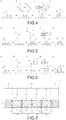
- a specific detection example will be described with reference to Figs. 1 to 3 .
- the biological substance S1 such as proteins and receptors (or those simulating receptors) is fixed to a holding surface 111 (see Part A of Fig. 1 ), and biological substance S2 to S4 for which the interaction with the biological substance S1 are checked are added, dyes such as fluorescent dyes F1 to F3 being respectively fixed to the biological substance S2 to S4 (see Part B in Fig. 1 ). Then, the biological substances S3 and S4 that have not interacted with the biological substance S1 are washed (see Part C of Fig. 1 ), and the fluorescent dye F1 is detected from the holding surface 111 (see Part D of Fig. 1 ), whereby the interaction between the biological substance S1 and the biological substance S2 can be detected.
- the biological substance S1 such as proteins and receptors (or those simulating receptors) is fixed to a holding surface 111 (see Part A of Fig. 1 )
- biological substance S2 to S4 for which the interaction with the biological substance S1 are checked are added, dyes such as fluorescent dyes F
- the biological substance S1 such as a cell is fixed to the holding surface 111, the light emitter F1 that is taken in via a transporter t of the biological substance S1 (e.g., a transporter in the cell membrane) can be detected.
- a transporter t of the biological substance S1 e.g., a transporter in the cell membrane
- a probe S5 including a DNA, an RNA, or the like is fixed to the holding surface 111 (see Part A of Fig. 2 ), and samples containing DNAs S6 and S7, which may be targets, and an intercalator I are added (see Part B of Fig. 2 ). Then, when the DNA S6 having a sequence complementary to the probe S5 is contained in the sample, a hybridization reaction occurs. The DNA S7 that has not been hybridized (see Part C of Fig. 2 ) is washed, and the light emitted from the intercalator I from the holding surface 111 is detected (see D in Fig. 2 ), whereby hybridization of the probe S5 and the target DNA S6 can be detected.
- a biological substance S8 is fixed to the holding surface 111 (see Part A of Fig. 3 ), and a biological substance S9 that interacts with the biological substance S8 to form a new substance S10 is added (see Part B of Fig. 3 ).
- a dye such as a fluorescent dye F4 that specifically binds to the substance S10 is added (see Part C of Fig. 3 ), and the fluorescent dye F4 is detected from the holding surface 111 (see Part D of Fig. 3 ), whereby the interaction between the biological substance S8 and the biological substance S9 can be detected.
- the present technology can be used to perform screening of substances, which may be agonists or antagonists of various receptors, and screening of inhibitors of the production of various microorganisms, antimicrobials, bactericides, and the like.
- substances which may be agonists or antagonists of various receptors
- screening of inhibitors of the production of various microorganisms, antimicrobials, bactericides, and the like A specific detection example will be described with reference to Figs. 4 to 6 .
- a receptor R1 (or those simulating the receptor R1) is fixed to the holding surface 111 (see Part A of Fig. 4 ), and substances d1 to d3 for checking the agonism of the receptor R1 are added, dyes such as fluorescent dyes F5 to F7 being respectively fixed to the substances d1 to d3 (see Part B of Fig. 4 ). Then, the substances d2 and d3 that have not bound to the receptor R1 are washed (see Part C of Fig. 4 ), and the fluorescent dye F5 is detected from the holding surface 111 (see Part D of Fig 3 ), whereby screening of the substance d1 that can be an agonist of the receptor R1 can be performed.
- a receptor R2 (or a those simulating the receptor R2) is fixed to the holding surface 111 (see Part A of Fig. 5 ), and a substance d4 for checking the antagonism of this receptor R2 is added (see Part B of Fig. 5 ).
- a ligand L1 that binds to the receptor R2 is added, a dye such as a fluorescent dye F8 being fixed to the ligand L1 (see Part C of Fig. 5 ).
- the substance d4 can be an antagonist of the receptor R2
- the ligand L1 cannot bind to the receptor R2 because the receptor R2 and the substance d4 are bound to each other (see Part C of Fig. 5 ).
- a receptor R3 (or those simulating the receptor R3) is fixed to the holding surface 111 (see Part A of Fig. 6 ), and a substance d5 for checking the antagonism of this receptor R3 is added (see Part B of Fig. 6 ).
- a ligand L2 that binds to the receptor R3 is added, a dye such as a fluorescent dye F9 being fixed to the ligand L2 (see Part C of Fig. 6 ).
- the substance d5 cannot be an antagonist of the receptor R3
- the ligand L2 binds to the receptor R3 (see Part D of Fig. 6 ).
- the fluorescent dye F9 is detected from the holding surface 111 (see Part E of Fig. 6 ).
- the presence or absence of detection of fluorescent dye F8 or the fluorescent dye F9 from the holding surface 111 can be used to perform screening of the substance d4 that can be an antagonist of the receptor R3.
- Chip 1 for detecting biological substance Chip 1 for detecting biological substance
- the chip 1 for detecting a biological substance includes a plurality of pixels 11, each of the pixels includes at least the holding surface 111 for holding the biological substance S and a photoelectric conversion unit 112 that is provided below the holding surface 111 and on a semiconductor substrate 12. Then, a color-mixture suppressing unit 13 is provided between the pixels 11.
- a color-mixture suppressing unit 13 is provided between the pixels 11.
- Fig. 7 is a schematic cross-sectional view schematically showing a first embodiment of the chip 1 for detecting a biological substance according to the present technology.
- the chip 1 for detecting a biological substance according to the first embodiment includes an effective pixel region 11E in which the plurality of pixels 11 is two-dimensionally arranged in a matrix.
- Each of the pixels 11 includes at least the holding surface 111 for holding the biological substance S and the photoelectric conversion unit 112.
- a photoelectric conversion element such as a photodiode can be freely used.
- each of the pixels 11 may include a pixel circuit including a charge accumulation unit, a plurality of transistors, a capacitive element, and the like.
- An optical black pixel, a wiring region, and the like may be provided on the outside O of the effective pixel region 11E.
- the holding surface 111 is not particularly limited as long as it has a configuration in which the biological substance S can be held, and surface treatment can be freely used.
- the holding surface 111 can be formed by applying a photosensitive silane coupling agent or the like, which is modified to be hydrophilic by being irradiated with ultraviolet rays and selectively irradiating a region in which the biological substance S is desired to be held with ultraviolet rays.
- the biological substance S such as a nucleic acid whose one end is biotinylated can be held by the avidin-biotin bond.
- a light-shielding film 17 described below, a partition wall, or the like is provided above (upper side of the chip surface) between the adjacent pixels 11 so that a liquid can be held on the surface of the chip 1, whereby the biological substance S can be held in the liquid.
- the color-mixture suppressing unit 13 is provided between the pixels 11.
- the pixel 11 and the color-mixture suppressing unit 13 have different conductivity types, color-mixture between the adjacent pixels 11 is suppressed.
- the pixel 11 has an N-type region and a space between the pixels 11 is a P-type region.
- the pixel 11 has a P-type region and the pixel 11 has an N-type region.
- the biological substance S is described for illustrative purposes, but the biological substance S is not encompassed in the chip 1 for detecting a biological substance according to the present technology.
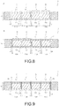
- Part A of Fig. 8 is a schematic cross-sectional view schematically showing a second embodiment of the chip 1 for detecting a biological substance according to the present technology
- Part B of Fig. 8 is a schematic cross-sectional view schematically showing a modified example of the second embodiment.
- the chip 1 for detecting a biological substance according to the second embodiment includes a trench 13T between photoelectric conversion regions 112A and this trench 13T functions as the color-mixture suppressing unit 13.
- an oxide film 14 may be provided inside the trench 13T.
- the material of the oxide film 14 include a material having a negative fixed charges, such as hafnium oxide (HfO 2 ), aluminum oxide (Al 2 O 3 ), and tantalum oxide (Ta 2 O 5 ).
- hafnium oxide (HfO 2 ) hafnium oxide (HfO 2 ), aluminum oxide (Al 2 O 3 ), and tantalum oxide (Ta 2 O 5 ).
- hafnium oxide HfO 2
- Al 2 O 3 aluminum oxide
- tantalum oxide Ta 2 O 5
- the oxide film 14, a metal 15, and the like can be provided inside the trench 13T.
- the metal 15 the light shielding effect can be enhanced, and it is possible to suppress color-mixture into the adjacent pixel and an erroneous determination.
- the oxide film 14 and the metal 15 inside the trench 13T it is possible to improve the color-mixture suppressing effect between the adjacent pixels 11 while suppressing the dark current.
- the oxide film described in Fig. 8 can be used. That is, a silicon oxide film (SiO 2 film), a hafnium oxide film (HfO 2 film), an aluminum oxide film (Al 2 O 3 film), a tantalum oxide film (Ta 2 O 5 film), and the like can be used.
- tungsten (W), aluminum (Al), copper (Cu), or titanium (Ti) can be used as the metal.
- Part A of Fig. 10 is a schematic cross-sectional view schematically showing a fourth embodiment of the chip 1 for detecting a biological substance according to the present technology.
- a recessed portion 111C is provided above the photoelectric conversion unit 112 and in the holding surface 111. By holding, on this recessed portion 111C, the biological substance S to be detected, light from the biological substance S can be prevented from scattering.
- the oxide film 14 may be provided in the recessed portion 111C.
- the oxide film 14 it is possible to eliminate a color-mixture path and improve the sensitivity.
- the shape of the recessed portion 111C is not particularly limited.
- the recessed portion 111C can be designed to have a substantially square shape in a cross-sectional view, a substantially trapezoidal shape in a cross-sectional view as shown in Part C of Fig. 10 , a substantially semicircular shape in a cross-sectional view although not shown, or the like.
- Fig. 11 is a schematic cross-sectional view schematically showing a fifth embodiment of the chip 1 for detecting a biological substance according to the present technology.
- the holding surface 111 is provided on a film 16 formed on the semiconductor substrate 12.
- an inorganic film such as a silicon oxide film (SiO 2 film), a silicon nitride film (Si 3 N 4 film), a silicon oxynitride film (SiON film), a hafnium oxide film (HfO film), an aluminum oxide film (Al 2 O 3 film), and a tantalum oxide film (Ta 2 O 5 film), or an organic film formed a resin material such as a styrene resin, an acrylic resin, a styrene-acrylic copolymer resin, and a siloxane resin can be selected.
- a resin material such as a styrene resin, an acrylic resin, a styrene-acrylic copolymer resin, and a siloxane resin
- the refractive index of the film 16 is different from that of the semiconductor substrate 12.
- the film 16 has a first refractive index and the semiconductor substrate 12 has a second refractive index different from the first refractive index.
- the refractive index of the film 16 and the refractive index of the semiconductor substrate 12 differ, enabling angular-dependent optical designs of reflectance.
- the light in the lateral direction can be reflected to prevent it from entering the semiconductor substrate 12. As a result, it is possible to suppress color-mixture between the pixels 11.
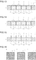
- the film 16 may also be included in the trench 13T described above, as in a sixth embodiment to an eighth embodiment shown in Figs. 12 to 14 . Further, the film 16 may be formed by stacking a plurality of films 16 or may be stacked with the oxide film 14 as in the eighth embodiment shown in Fig. 14 , in accordance with the purpose.
- Fig. 15 is a schematic cross-sectional view schematically showing a ninth embodiment of the chip 1 for detecting a biological substance according to the present technology.
- the chip 1 for detecting a biological substance according to the ninth embodiment includes the light-shielding film 17 provided above between the adjacent pixels 11. By providing the light-shielding film 17, it is possible to further suppress color-mixture between the pixels 11. Further, by providing the light-shielding film 17, it is possible to hold a liquid sample on the holding surface 111 and hold the biological substance S in the liquid.
- a film can be freely selected as long as it is a film formed of a material capable of blocking light.
- a metallic film such as tungsten (W), aluminum (Al), copper (Cu), and titanium (Ti), or an optical black filter can be used.
- the form of the light-shielding film 17 is not particularly limited and can be freely designed in accordance with the purpose. However, as shown in Parts A to C of Fig. 16 , it is favorable that the light-shielding film 17 (i.e., the holding surface 111) has one or more shapes selected from a circular shape, an elliptical shape, and a polygon having round corners in a top view. By eliminating the corner in a top view between the light-shielding films 17 as described above, it is possible to suppress unevenness in the supply of the samples to the holding surface 111 when the samples are supplied, and insufficient washing when the holding surface 111 is washed. As a result, it is possible to further improve the detection accuracy.
- a method of providing a flattening film 19 using an organic film or the like can be employed, as in a tenth embodiment shown in Fig. 17 .
- Another film such as the oxide film 14 may be provided below the light-shielding film 17 as in an eleventh embodiment shown in Fig. 18 . Further, the light-shielding film 17 can also be embedded in the trench 13T described above to form a light shielding wall from above between the pixels 11 to the semiconductor substrate 12, as in a twelfth embodiment shown in Fig. 19 .
- the light-shielding film 17 may be provided for each of the pixels 11, but the light-shielding film 17 may be provided for a plurality of pixels 11.
- Fig. 20 is a schematic cross-sectional view schematically showing a thirteenth embodiment of the chip 1 for detecting a biological substance according to the present technology.
- the holding surface 111 is provided above an on-chip lens (OCL) 18 provided on the semiconductor substrate 12.
- OCL on-chip lens
- the specific structure of the on-chip lens (OCL) 18 is not particularly limited, and a structure (antireflection layer or the like) of an on-chip lens (OCL) can be freely selected and used.
- the on-chip lens (OCL) 18 may include the flattening film 19 as in a fourteenth embodiment shown in Fig. 21 .
- the holding surface 111 may be provided on the flattening film 19 formed on the on-chip lens (OCL) 18.
- a flattening film 19a for flattening the light-shielding film 17 and a flattening film 19b for flattening the on-chip lens (OCL) are provided.
- the flattening films 19a and 19b may be formed of different materials or may be formed of the same material.
- Fig. 22 is a schematic cross-sectional view schematically showing a fifteenth embodiment of the chip 1 for detecting a biological substance according to the present technology.
- the chip 1 for detecting a biological substance according to the fifteenth embodiment includes a protective film 20 on the surface of the chip. By providing the protective film 20, it is possible to improve weatherability to heat, light, water, acids, alkalis, agents, and the like, and can also be contacted with water, acids, alkalis, or agents for extended periods of time.
- any material having weatherability to heat, light, water, acids, alkalis, medicines, and the like can be freely selected and used in accordance with the purpose.
- examples thereof include silicon oxide (SiO 2 ) , silicon nitride (Si 3 N 4 ), and silicon oxynitride (SiON).
- Fig. 23 is a schematic cross-sectional view schematically showing a sixteenth embodiment of the chip 1 for detecting a biological substance according to the present technology.
- the chip 1 for detecting a biological substance according to the sixth embodiment includes an excitation light cut filter 21. By providing the excitation light cut filter 21, the excitation light can be prevented from leaking into the photoelectric conversion unit 112. As a result, it is possible to further improve the detection accuracy.
- Fig. 24 is a schematic top plan view schematically showing a seventeenth embodiment of the chip 1 for detecting a biological substance according to the present technology.
- Fig. 25 is a schematic cross-sectional view taken along line A-A of Fig. 24 omitting the inner structure.
- the chip 1 for detecting a biological substance according to the seventeenth embodiment includes a stepped portion 22a is provided on the outside O of the effective pixel region 11E. More specifically, in the chip 1 for detecting a biological substance according to the seventeenth embodiment, an intermediate region 22, a wiring region 23, and a peripheral region 24 are provided from the effective pixel region 11E toward the outside, and the stepped portion 22a is provided in the intermediate region 22.
- the wiring region 23 provided on the outside O of the effective pixel region 11E is generally stepped.
- the stepped portion 22a in the intermediate region 22 between the wiring region 23 and the effective pixel region11E it is possible to suppress unevenness in the supply of the samples to the holding surface 111 when the samples are supplied, insufficient washing when the holding surface 111 is washed, and the like. As a result, it is possible to further improve the detection accuracy.
- the corners of the stepped portion 22a are formed in a round shape in a top view.
- the corners of the stepped portion 22a are formed in a round shape, it is possible to further suppress unevenness in the supply of the samples to the holding surface 111 when the samples are supplied, insufficient washing when the holding surface 111 is washed, and the like.
- the corners of the wiring region 23 can be formed in a round shape in a top view.
- a step portion can be provided in the peripheral region 24.
- Fig. 26 is a block diagram showing the concept of the biological-substance detection apparatus 2 according to the present technology.
- the biological-substance detection apparatus 2 according to the present technology includes at least the above-mentioned chip 1 for detecting a biological substance according to the present technology, and an analysis unit 21. Further, the biological-substance detection apparatus 2 may further include a light irradiation unit 22, a storage unit 23, a display unit 24, a temperature control unit 25, and the like in accordance with the purpose. The respective units will be described below. Note that since the chip 1 for detecting a biological substance is as described above, description thereof is omitted here.
- the electric information acquired by the chip 1 for detecting a biological substance is analyzed. For example, on the basis of the electric information acquired by the chip 1 for detecting a biological substance, screening of the presence or absence of the biological substance S, the presence or absence of an interaction in the biological substance S, a medicinal active ingredient, and the like is performed.
- the analysis unit 21 may be implemented by a personal computer or a CPU, and may be stored as a program in a hardware resource including a recording medium (e.g., a non-volatile memory (USB memory), an HDD, or a CD) and operated by a personal computer or a CPU.
- a recording medium e.g., a non-volatile memory (USB memory), an HDD, or a CD
- the biological-substance detection apparatus 2 may include the light irradiation unit 22 for applying excitation light, for example.
- the biological substance S held on the holding surface 111 of the chip for detecting a biological substance1 is irradiated with light.
- the light irradiation unit 22 does not necessarily need to be provided, and the biological substance S can be irradiated with light using an external light irradiation device or the like.
- the type of the light emitted from the light irradiation unit 22 is not particularly limited, but light having a constant light direction, wavelength, and light intensity is desirable in order to reliably generate fluorescent light or scattered light from fine particles.
- Examples thereof include lasers and LEDs.
- the type of the laser is not particularly limited, and one or two or more of an argon ion (Ar) laser, a helium-neon (He-Ne) laser, a dye laser, a krypton (Cr) laser, a semiconductor laser, or a solid-state laser combining a semiconductor laser and a wavelength-conversion optical element, and the like can be freely used in combination.
- the light irradiation unit 22 may include a plurality of light irradiation units 22 in accordance with the purpose. For example, one light irradiation unit 22 may be provided for each of the pixels 11 of the chip 1 for detecting a biological substance. Further, by stacking a substrate in which light-emitting elements such as LEDs are arranged at positions corresponding to the pixels 11 of the chip 1 for detecting a biological substance on the chip 1 for detecting a biological substance, the biological substance S can be irradiated with light.
- the biological-substance detection apparatus 2 may include the storage unit 23 that stores various types of information.
- the storage unit 23 is capable of storing all items relating to detection, such as the electric data acquired by the chip 1 for detecting a biological substance, the analysis data generated by the analysis unit 21, and the optical data obtained by irradiation by the light irradiation unit 22.
- the storage unit 23 does not necessarily need to be provided and an external storage device may be connected.
- an external storage device for example, a hard disk or the like can be used.
- the biological-substance detection apparatus 2 may include the display unit 24 that displays various types of information.
- the display unit 24 all items relating to detection, such as the electric data acquired by the chip 1 for detecting a biological substance, the analysis data generated by the analysis unit 21, the optical data obtained by irradiation by the light irradiation unit 22, and the data stored in the storage unit 23, can be displayed.
- the display unit 24 does not necessarily need to be provided, and an external display device may be connected.
- the display unit 24 for example, a display, a printer, or the like can be used.
- the biological-substance detection apparatus 2 may include a temperature control unit 25 for keeping the biological substance S held on the holding surface 111 of the chip 1 for detecting a biological substance at a predetermined temperature or for heating or cooling the biological substance S to a predetermined temperature.
- a temperature control unit 25 for keeping the biological substance S held on the holding surface 111 of the chip 1 for detecting a biological substance at a predetermined temperature or for heating or cooling the biological substance S to a predetermined temperature.
- the biological substance S is an enzyme
- temperature control can be performed so as to keep the optimum temperature by the temperature control unit 25.
- the temperature control unit 25 can be controlled by the temperature control unit 25 so as to keep it within a temperature range in which hybridization can be performed.
- a thermoelectric element such as a Peltier element can be used as the temperature control unit 25 .
- the temperature control unit 25 may include a plurality of temperature control units 25 in accordance with the purpose. For example, one temperature control unit 25 may be provided for each of the pixels 11 of the chip 1 for detecting a biological substance. Further, by stacking a substrate in which thermoelectric elements are arranged at positions corresponding to the pixels 11 of the chip 1 for detecting a biological substance on the pixels 11 of the chip 1 for detecting a biological substance, temperature control can be performed on the biological substance S.
- the temperature control unit 25 does not necessarily need to be provided, and an external temperature control device or the like may be used to perform temperature control of the biological substance S.
- Fig. 27 is a block diagram showing the concept of the biological-substance detection system 3 according to the present technology.
- the biological-substance detection system 3 according to the present technology includes at least the above-mentioned chip 1 for detecting a biological substance according to the present technology, and an analysis device 31
- the biological-substance detection system 3 may further include a light irradiation device 32, a storage device 33, a display device 34, a temperature control device 35, and the like in accordance with the purpose.
- the chip 1 for detecting a biological substance and the respective devices may be connected to each other via wired or radio networks. Note that the details of each device are the same as the details of each unit of the biological-substance detection apparatus 2 according to the present technology, and therefore description thereof will be omitted here.
Landscapes
- Physics & Mathematics (AREA)
- Health & Medical Sciences (AREA)
- Chemical & Material Sciences (AREA)
- Spectroscopy & Molecular Physics (AREA)
- General Physics & Mathematics (AREA)
- Life Sciences & Earth Sciences (AREA)
- Analytical Chemistry (AREA)
- General Health & Medical Sciences (AREA)
- Immunology (AREA)
- Pathology (AREA)
- Biochemistry (AREA)
- Engineering & Computer Science (AREA)
- Chemical Kinetics & Catalysis (AREA)
- Nuclear Medicine, Radiotherapy & Molecular Imaging (AREA)
- Mathematical Physics (AREA)
- Dispersion Chemistry (AREA)
- Hematology (AREA)
- Clinical Laboratory Science (AREA)
- Biomedical Technology (AREA)
- Molecular Biology (AREA)
- Theoretical Computer Science (AREA)
- Apparatus Associated With Microorganisms And Enzymes (AREA)
- Investigating, Analyzing Materials By Fluorescence Or Luminescence (AREA)
- Investigating Or Analysing Biological Materials (AREA)
- Optical Measuring Cells (AREA)
- Light Receiving Elements (AREA)
Abstract
Description
- The present technology relates to a chip for detecting a biological substance, a biological-substance detection apparatus, and a biological-substance detection system.
- In recent years, technological studies on genetic analysis, protein analysis, cellular analysis, etc. have been promoted in various fields such as medical field, drug discovery field, clinical examination field, food field, agricultural field, and engineering field. In particular, recently, detection technologies on a chip typified by a lab-on chip in which various reactions such as detection and analysis of biological substances such as nucleic acids, proteins, cells, and microorganisms are performed in a microscale channel or a well provided in a chip, been developed and put into practical use. These technologies have attracted attention as a method of easily measuring biological substances and the like.
- For example,
Patent Literature 1 discloses an optical detection apparatus including at least a first substrate in which a plurality of wells is formed; a second substrate provided with a heating means so as to be in contact with the well; a third substrate provided with a plurality of light irradiation means positioned corresponding to positions of the wells; and a fourth substrate provided with a plurality of light detection means positioned corresponding to the positions of the wells. In this optical detection apparatus, various reactions progressing in each well can be measured. - Further, for example,
Patent Literature 2 discloses a chemical sensor including: a substrate in which an optical detection unit is formed; and a plasmon absorbing layer having a metallic nanostructure for giving a plasmon absorbing property, which is stacked on the substrate. In this chemical sensor, it is possible to detect the light emission caused by the bond of a probe material fixed on the sensor and a target material. -
- Patent Literature 1:
Japanese Patent Application Laid-open No. 2010-284152 - Patent Literature 2:
WO2013/080473 - In the case where light emitted from a biological substance is detected in a plurality of regions (e.g., a plurality of wells) on a chip using a plurality of light detection units corresponding to the regions, there is a problem of leakage of light from an adjacent region into each of the light detection units. For example, in the case where different reactions are caused to progress in the respective regions and the light emission caused by each of the reactions is detected, there is a possibility that an erroneous determination is made by erroneously detecting the light emission from another region.
- In this regard, it is a main object of the present technology to provide a chip for detecting a biological substance with high detection accuracy.
- That is, in the present technology, first, there is provided a chip for detecting a biological substance, including:
- a plurality of pixels, in which
- each of the pixels includes at least a holding surface for holding the biological substance and a photoelectric conversion unit that is provided below the holding surface and on a semiconductor substrate, and
- a color-mixture suppressing unit is provided between the pixels.
- In the chip for detecting a biological substance according to the present technology, the pixel and the color-mixture suppressing unit may have different conductivity types
- In this case, the pixel may have an N-type region and the color-mixture suppressing unit may have a P-type region. Conversely, the pixel may have a P-type region and the color-mixture suppressing unit may have an N-type region.
- In the chip for detecting a biological substance according to the present technology, each of the plurality of pixels may have a photoelectric conversion region, and a trench may be provided between the respective photoelectric conversion regions.
- In this case, an interior of the trench may include one or more selected from an oxide film and a metal.
- In the chip for detecting a biological substance according to the present technology, a recessed portion may be provided above the photoelectric conversion unit and on the holding surface.
- In the chip for detecting a biological substance according to the present technology, the holding surface may be provided on a film formed on the semiconductor substrate.
- In this case, the film may have a first refractive index and the semiconductor substrate may have a second refractive index different from the first refractive index.
- Further, the film may include one or more films selected from an inorganic film and an organic film.
- The chip for detecting a biological substance according to the present technology may further include light-shielding films provided above between the respective adjacent pixels.
- A space between the light-shielding films may be formed to have one or more shapes selected from a circular shape, an elliptical shape, and a polygon having round corners in a top view.
- In the chip for detecting a biological substance according to the present technology, the holding surface may be provided on an on-chip lens (OCL) provided on the semiconductor substrate.
- In this case, the holding surface may also be provided on a flattening film formed on the on-chip lens (OCL).
- Examples of a biological substance that can be detected by the chip for detecting a biological substance according to the present technology include one or more biological substances selected from nucleic acids, proteins, cells, microorganisms, chromosomes, liposomes, mitochondria, organelles, and complexes thereof.
- Further, the present technology, there is provided a biological-substance detection apparatus including:
- a chip for detecting a biological substance including a plurality of pixels; and
- an analysis unit that analyzes electric information acquired by the chip for detecting a biological substance, in which
- each of the pixels includes at least a holding surface for holding the biological substance and a photoelectric conversion unit that is provided below the holding surface and on a semiconductor substrate, and
- a color-mixture suppressing unit is provided between the pixels.
- Further, in the present technology, there is provided a biological-substance detection system including:
- a chip for detecting a biological substance including a plurality of pixels; and
- an analysis device that analyzes electric information acquired by the chip for detecting a biological substance, in which
- each of the pixels includes at least a holding surface for holding the biological substance and a photoelectric conversion unit that is provided below the holding surface and on a semiconductor substrate, and
- a color-mixture suppressing unit is provided between the pixels.
- In the present technology, the "biological substance" is intended to broadly include nucleic acids, proteins, cells, microorganisms, chromosomes, liposomes, mitochondria, organelles, and complexes thereof. The cells include animal cells (e.g., hematopoietic cells) and plant cells. The microorganisms include bacteria such as Escherichia coli, viruses such as tobacco mosaic virus, and fungi such as yeast.
-
- [
Fig. 1] Fig. 1 is a schematic conceptual diagram schematically showing an interaction of a biological substance S that can be detected by a chip for detecting abiological substance 1, a biological-substance detection apparatus 2, and a biological-substance detection system 3 according to the present technology. - [
Fig. 2] Fig. 2 is a schematic conceptual diagram schematically showing an interaction of the biological substance S that can be detected by the chip for detecting abiological substance 1, the biological-substance detection apparatus 2, and the biological-substance detection system 3 according to the present technology. - [
Fig. 3] Fig. 3 is a schematic conceptual diagram schematically showing an interaction of the biological substance S that can be detected by the chip for detecting abiological substance 1, the biological-substance detection apparatus 2, and the biological-substance detection system 3 according to the present technology. - [
Fig. 4] Fig. 4 is a schematic conceptual diagram schematically showing screening of another substance that can be performed by the chip for detecting abiological substance 1, the biological-substance detection apparatus 2, and the biological-substance detection system 3 according to the present technology. - [
Fig. 5] Fig. 5 is a schematic conceptual diagram schematically showing screening of another substance that can be performed by the chip for detecting abiological substance 1, the biological-substance detection apparatus 2, and the biological-substance detection system 3 according to the present technology. - [
Fig. 6] Fig. 6 is a schematic conceptual diagram schematically showing screening of another substance that can be performed by the chip for detecting abiological substance 1, the biological-substance detection apparatus 2, and the biological-substance detection system 3 according to the present technology. - [
Fig. 7] Fig. 7 is a schematic cross-sectional view schematically showing a first embodiment of thechip 1 for detecting a biological substance according to the present technology. - [
Fig. 8 ] Part A ofFig. 8 is a schematic cross-sectional view schematically showing a second embodiment of thechip 1 for detecting a biological substance according to the present technology, and Part B ofFig. 8 is a schematic cross-sectional view schematically showing a modified example of the second embodiment. - [
Fig. 9] Fig. 9 is a schematic cross-sectional view schematically showing a third embodiment of thechip 1 for detecting a biological substance according to the present technology. - [
Fig. 10] Fig. 10 is a schematic cross-sectional view schematically showing a fourth embodiment of thechip 1 for detecting a biological substance according to the present technology. - [
Fig. 11] Fig. 11 is a schematic cross-sectional view schematically showing a fifth embodiment of thechip 1 for detecting a biological substance according to the present technology. - [
Fig. 12] Fig. 12 is a schematic cross-sectional view schematically showing a sixth embodiment of thechip 1 for detecting a biological substance according to the present technology. - [
Fig. 13] Fig. 13 is a schematic cross-sectional view schematically showing a seventh embodiment of thechip 1 for detecting a biological substance according to the present technology. - [
Fig. 14] Fig. 14 is a schematic cross-sectional view schematically showing a eighth embodiment of thechip 1 for detecting a biological substance according to the present technology. - [
Fig. 15] Fig. 15 is a schematic cross-sectional view schematically showing a ninth embodiment of thechip 1 for detecting a biological substance according to the present technology. - [
Fig. 16] Fig. 16 is a schematic top plan view schematically showing an example of a light-shieldingfilm 17 of thechip 1 for detecting a biological substance according to the present technology. - [
Fig. 17] Fig. 17 is a schematic cross-sectional view schematically showing a tenth embodiment of thechip 1 for detecting a biological substance according to the present technology. - [
Fig. 18] Fig. 18 is a schematic cross-sectional view schematically showing an eleventh embodiment of thechip 1 for detecting a biological substance according to the present technology. - [
Fig. 19] Fig. 19 is a schematic cross-sectional view schematically showing a twelfth embodiment of thechip 1 for detecting a biological substance according to the present technology. - [
Fig. 20] Fig. 20 is a schematic cross-sectional view schematically showing a thirteenth embodiment of thechip 1 for detecting a biological substance according to the present technology. - [
Fig. 21] Fig. 21 is a schematic cross-sectional view schematically showing a fourteenth embodiment of thechip 1 for detecting a biological substance according to the present technology. - [
Fig. 22] Fig. 22 is a schematic cross-sectional view schematically showing a fifteenth embodiment of thechip 1 for detecting a biological substance according to the present technology. - [
Fig. 23] Fig. 23 is a schematic cross-sectional view schematically showing a sixteenth embodiment of thechip 1 for detecting a biological substance according to the present technology. - [
Fig. 24] Fig. 24 is a schematic top plan view schematically showing a seventeenth embodiment of thechip 1 for detecting a biological substance according to the present technology. - [
Fig. 25]Fig. 25 is a schematic cross-sectional view taken along line A-A ofFig. 24 omitting the inner structure. - [
Fig. 26] Fig. 26 is a block diagram showing the concept of the biological-substance detection apparatus 2 according to the present technology. - [
Fig. 27] Fig. 27 is a block diagram showing the concept of the biological-substance detection system 3 according to the present technology. - Hereinafter, favorable embodiments for carrying out the present technology will be described with reference to the accompanying drawings. The embodiments described below illustrate an example of a typical embodiment of the present technology, which does not narrowly interpret the scope of the present technology. Note that description will be made in the following order.
- 1. Outline of detection of biological substance in present technology
- (1) Detection of biological substance S itself
- (2) Detection of interaction of biological substance S
- (3) Screening of other substances
- 2.
Chip 1 for detecting biological substance- (1) First Embodiment
- (2) Second Embodiment, Third Embodiment
- (3) Fourth Embodiment
- (4) Fifth Embodiment to Seventh Embodiment
- (5) Ninth Embodiment to Twelfth embodiment
- (6) Thirteenth embodiment, Fourteenth embodiment
- (7) Fifteenth embodiment
- (8) Sixteenth embodiment
- (9) Seventeenth embodiment
- 3. Biological-
substance detection apparatus 2 - 4. Biological-
substance detection system 3 - The outline of detection a biological substance S performed by a
chip 1 for detecting a biological substance1, a biological-substance detection apparatus 2, and a biological-substance detection system 3 according to the present technology will be described. Thechip 1 for detecting a biological substance, the biological-substance detection apparatus 2, and the biological-substance detection system 3 according to the present technology can be used for (1) detection of the biological substance S itself, (2) detection of an interaction of the biological substance S, (3) screening of another substance (e.g., medicinal active ingredient) using the biological substance S, and the like. Note that the respective detections are performed by a holdingsurface 111 of thechip 1 for detecting a biological substance to be described later. - For example, the present technology can be used to detect biological substances such as erythrocytes, leukocytes, platelets, cytokines, hormonal substances, sugars, lipids, and proteins, which are contained in body fluid such as blood, urine, stool, and saliva; microorganisms such as bacteria, fungi, and viruses in body fluid and water; genes in cells and microorganisms, and the like. For example, after staining using a dye that specifically acts on a substance to be detected or a material to be not detected, the presence of the substance to be detected can be detected by the presence or absence of the target photodetection. The detected result can be used for diagnosis of a disease, diagnosis of a body environment, examination of water quality, and the like.
- For example, the present technology can be used to detect interactions such as interactions of proteins, hybridizations of nucleic acids, and binding of cytokines or hormonal substances to receptors. A specific detection example will be described with reference to
Figs. 1 to 3 . - For example, as shown in Part A to D of
Fig. 1 , the biological substance S1 such as proteins and receptors (or those simulating receptors) is fixed to a holding surface 111 (see Part A ofFig. 1 ), and biological substance S2 to S4 for which the interaction with the biological substance S1 are checked are added, dyes such as fluorescent dyes F1 to F3 being respectively fixed to the biological substance S2 to S4 (see Part B inFig. 1 ). Then, the biological substances S3 and S4 that have not interacted with the biological substance S1 are washed (see Part C ofFig. 1 ), and the fluorescent dye F1 is detected from the holding surface 111 (see Part D ofFig. 1 ), whereby the interaction between the biological substance S1 and the biological substance S2 can be detected. - For example, as shown in Parts E to H of
Fig. 1 , the biological substance S1 such as a cell is fixed to the holdingsurface 111, the light emitter F1 that is taken in via a transporter t of the biological substance S1 (e.g., a transporter in the cell membrane) can be detected. - For example, as shown in Parts A to D of
Fig. 2 , a probe S5 including a DNA, an RNA, or the like is fixed to the holding surface 111 (see Part A ofFig. 2 ), and samples containing DNAs S6 and S7, which may be targets, and an intercalator I are added (see Part B ofFig. 2 ). Then, when the DNA S6 having a sequence complementary to the probe S5 is contained in the sample, a hybridization reaction occurs. The DNA S7 that has not been hybridized (see Part C ofFig. 2 ) is washed, and the light emitted from the intercalator I from the holdingsurface 111 is detected (see D inFig. 2 ), whereby hybridization of the probe S5 and the target DNA S6 can be detected. - For example, as shown in Parts A to D of
Fig. 3 , a biological substance S8 is fixed to the holding surface 111 (see Part A ofFig. 3 ), and a biological substance S9 that interacts with the biological substance S8 to form a new substance S10 is added (see Part B ofFig. 3 ). Next, a dye such as a fluorescent dye F4 that specifically binds to the substance S10 is added (see Part C ofFig. 3 ), and the fluorescent dye F4 is detected from the holding surface 111 (see Part D ofFig. 3 ), whereby the interaction between the biological substance S8 and the biological substance S9 can be detected. - For example, the present technology can be used to perform screening of substances, which may be agonists or antagonists of various receptors, and screening of inhibitors of the production of various microorganisms, antimicrobials, bactericides, and the like. A specific detection example will be described with reference to
Figs. 4 to 6 . - For example, as shown in Parts A to D of
Fig. 4 , a receptor R1 (or those simulating the receptor R1) is fixed to the holding surface 111 (see Part A ofFig. 4 ), and substances d1 to d3 for checking the agonism of the receptor R1 are added, dyes such as fluorescent dyes F5 to F7 being respectively fixed to the substances d1 to d3 (see Part B ofFig. 4 ). Then, the substances d2 and d3 that have not bound to the receptor R1 are washed (see Part C ofFig. 4 ), and the fluorescent dye F5 is detected from the holding surface 111 (see Part D ofFig 3 ), whereby screening of the substance d1 that can be an agonist of the receptor R1 can be performed. - For example, as shown in Parts A to E of
Fig. 5 , a receptor R2 (or a those simulating the receptor R2) is fixed to the holding surface 111 (see Part A ofFig. 5 ), and a substance d4 for checking the antagonism of this receptor R2 is added (see Part B ofFig. 5 ). Next, a ligand L1 that binds to the receptor R2 is added, a dye such as a fluorescent dye F8 being fixed to the ligand L1 (see Part C ofFig. 5 ). At this time, in the case where the substance d4 can be an antagonist of the receptor R2, the ligand L1 cannot bind to the receptor R2 because the receptor R2 and the substance d4 are bound to each other (see Part C ofFig. 5 ). Even when an attempt is made to detect the fluorescent dye F8 from the holdingsurface 111 after washing the ligand L1 that has not bound to the receptor R2 in this state (see Part D ofFig. 5 ), no light is detected because the fluorescent dye F8 is not present on the holdingsurface 111 by washing (see Part E ofFig. 5 ). - Meanwhile, for example, as shown in Parts A to E of
Fig. 6 , a receptor R3 (or those simulating the receptor R3) is fixed to the holding surface 111 (see Part A ofFig. 6 ), and a substance d5 for checking the antagonism of this receptor R3 is added (see Part B ofFig. 6 ). Next, a ligand L2 that binds to the receptor R3 is added, a dye such as a fluorescent dye F9 being fixed to the ligand L2 (see Part C ofFig. 6 ). At this time, in the case where the substance d5 cannot be an antagonist of the receptor R3, the ligand L2 binds to the receptor R3 (see Part D ofFig. 6 ). When the substance d5 that has not bound to the receptor R3 is washed (see Part D ofFig. 6 ), the fluorescent dye F9 is detected from the holding surface 111 (see Part E ofFig. 6 ). - In this way, as shown in
Fig. 5 and Fig. 6 , the presence or absence of detection of fluorescent dye F8 or the fluorescent dye F9 from the holdingsurface 111 can be used to perform screening of the substance d4 that can be an antagonist of the receptor R3. - The
chip 1 for detecting a biological substance according to the present technology includes a plurality ofpixels 11, each of the pixels includes at least the holdingsurface 111 for holding the biological substance S and aphotoelectric conversion unit 112 that is provided below the holdingsurface 111 and on asemiconductor substrate 12. Then, a color-mixture suppressing unit 13 is provided between thepixels 11. Hereinafter, description will be made with reference to each embodiment. -
Fig. 7 is a schematic cross-sectional view schematically showing a first embodiment of thechip 1 for detecting a biological substance according to the present technology. Thechip 1 for detecting a biological substance according to the first embodiment includes aneffective pixel region 11E in which the plurality ofpixels 11 is two-dimensionally arranged in a matrix. Each of thepixels 11 includes at least the holdingsurface 111 for holding the biological substance S and thephotoelectric conversion unit 112. For thephotoelectric conversion unit 112, for example, a photoelectric conversion element such as a photodiode can be freely used. Further, although not illustrated, each of thepixels 11 may include a pixel circuit including a charge accumulation unit, a plurality of transistors, a capacitive element, and the like. An optical black pixel, a wiring region, and the like (not shown) may be provided on the outside O of theeffective pixel region 11E. - The holding
surface 111 is not particularly limited as long as it has a configuration in which the biological substance S can be held, and surface treatment can be freely used. For example, the holdingsurface 111 can be formed by applying a photosensitive silane coupling agent or the like, which is modified to be hydrophilic by being irradiated with ultraviolet rays and selectively irradiating a region in which the biological substance S is desired to be held with ultraviolet rays. Further, for example, when the holdingsurface 111 is subjected to avidin treatment, the biological substance S such as a nucleic acid whose one end is biotinylated can be held by the avidin-biotin bond. - Further, a light-shielding
film 17 described below, a partition wall, or the like is provided above (upper side of the chip surface) between theadjacent pixels 11 so that a liquid can be held on the surface of thechip 1, whereby the biological substance S can be held in the liquid. - The color-
mixture suppressing unit 13 is provided between thepixels 11. In the first embodiment of thechip 1 for detecting a biological substance according to the present technology, by making thepixel 11 and the color-mixture suppressing unit 13 have different conductivity types, color-mixture between theadjacent pixels 11 is suppressed. Specifically, for example, thepixel 11 has an N-type region and a space between thepixels 11 is a P-type region. Conversely, thepixel 11 has a P-type region and thepixel 11 has an N-type region. As a result, the color-mixture between theadjacent pixels 11 can be suppressed. - Note that, in the first embodiment shown in
Fig. 7 , the biological substance S is described for illustrative purposes, but the biological substance S is not encompassed in thechip 1 for detecting a biological substance according to the present technology. - Part A of
Fig. 8 is a schematic cross-sectional view schematically showing a second embodiment of thechip 1 for detecting a biological substance according to the present technology, and Part B ofFig. 8 is a schematic cross-sectional view schematically showing a modified example of the second embodiment. Thechip 1 for detecting a biological substance according to the second embodiment includes atrench 13T betweenphotoelectric conversion regions 112A and thistrench 13T functions as the color-mixture suppressing unit 13. - As shown in Part B of
Fig. 8 , anoxide film 14 may be provided inside thetrench 13T. Examples of the material of theoxide film 14 include a material having a negative fixed charges, such as hafnium oxide (HfO2), aluminum oxide (Al2O3), and tantalum oxide (Ta2O5). One of these oxide films may be provided as a single film, or a plurality of films may be stacked and provided. By providing an oxide film, it is suppress a dark current and an erroneous determination. - Inside the
trench 13T, as in the third embodiment shown inFig. 9 , theoxide film 14, ametal 15, and the like can be provided. By providing themetal 15, the light shielding effect can be enhanced, and it is possible to suppress color-mixture into the adjacent pixel and an erroneous determination. By providing theoxide film 14 and themetal 15 inside thetrench 13T, it is possible to improve the color-mixture suppressing effect between theadjacent pixels 11 while suppressing the dark current. - As the
oxide film 14, the oxide film described inFig. 8 can be used. That is, a silicon oxide film (SiO2 film), a hafnium oxide film (HfO2 film), an aluminum oxide film (Al2O3 film), a tantalum oxide film (Ta2O5 film), and the like can be used. - As the metal, for example, tungsten (W), aluminum (Al), copper (Cu), or titanium (Ti) can be used.
- Note that in the second embodiment and the third embodiment, the other structures are the same as those in the first embodiment described above, and therefore description thereof will be omitted here. Also in other embodiments, only portions different from those in the first embodiment will be described below.
- Part A of
Fig. 10 is a schematic cross-sectional view schematically showing a fourth embodiment of thechip 1 for detecting a biological substance according to the present technology. In thechip 1 for detecting a biological substance according to the fourth embodiment, a recessedportion 111C is provided above thephotoelectric conversion unit 112 and in the holdingsurface 111. By holding, on this recessedportion 111C, the biological substance S to be detected, light from the biological substance S can be prevented from scattering. - As shown in Part B of
Fig. 10 , theoxide film 14 may be provided in the recessedportion 111C. By providing theoxide film 14, it is possible to eliminate a color-mixture path and improve the sensitivity. - Further, the shape of the recessed
portion 111C is not particularly limited. In addition to the substantially triangular shape in a cross-sectional view as shown in Parts A and B ofFig. 10 , the recessedportion 111C can be designed to have a substantially square shape in a cross-sectional view, a substantially trapezoidal shape in a cross-sectional view as shown in Part C ofFig. 10 , a substantially semicircular shape in a cross-sectional view although not shown, or the like. -
Fig. 11 is a schematic cross-sectional view schematically showing a fifth embodiment of thechip 1 for detecting a biological substance according to the present technology. In thechip 1 for detecting a biological substance according to the fifth embodiment, the holdingsurface 111 is provided on afilm 16 formed on thesemiconductor substrate 12. - As the
film 16, one or two or more kinds of films formed on thesemiconductor substrate 12 can be freely selected in accordance with the purpose. For example, an inorganic film such as a silicon oxide film (SiO2 film), a silicon nitride film (Si3N4 film), a silicon oxynitride film (SiON film), a hafnium oxide film (HfO film), an aluminum oxide film (Al2O3 film), and a tantalum oxide film (Ta2O5 film), or an organic film formed a resin material such as a styrene resin, an acrylic resin, a styrene-acrylic copolymer resin, and a siloxane resin can be selected. - It is favorable that the refractive index of the
film 16 is different from that of thesemiconductor substrate 12. In other words, it is favorable that thefilm 16 has a first refractive index and thesemiconductor substrate 12 has a second refractive index different from the first refractive index. The refractive index of thefilm 16 and the refractive index of thesemiconductor substrate 12 differ, enabling angular-dependent optical designs of reflectance. Of the light from the biological substance S held on the holdingsurface 111, the light in the lateral direction can be reflected to prevent it from entering thesemiconductor substrate 12. As a result, it is possible to suppress color-mixture between thepixels 11. - The
film 16 may also be included in thetrench 13T described above, as in a sixth embodiment to an eighth embodiment shown inFigs. 12 to 14 . Further, thefilm 16 may be formed by stacking a plurality offilms 16 or may be stacked with theoxide film 14 as in the eighth embodiment shown inFig. 14 , in accordance with the purpose. -
Fig. 15 is a schematic cross-sectional view schematically showing a ninth embodiment of thechip 1 for detecting a biological substance according to the present technology. Thechip 1 for detecting a biological substance according to the ninth embodiment includes the light-shieldingfilm 17 provided above between theadjacent pixels 11. By providing the light-shieldingfilm 17, it is possible to further suppress color-mixture between thepixels 11. Further, by providing the light-shieldingfilm 17, it is possible to hold a liquid sample on the holdingsurface 111 and hold the biological substance S in the liquid. - As the light-shielding
film 17, a film can be freely selected as long as it is a film formed of a material capable of blocking light. For example, a metallic film such as tungsten (W), aluminum (Al), copper (Cu), and titanium (Ti), or an optical black filter can be used. - The form of the light-shielding
film 17 is not particularly limited and can be freely designed in accordance with the purpose. However, as shown in Parts A to C ofFig. 16 , it is favorable that the light-shielding film 17 (i.e., the holding surface 111) has one or more shapes selected from a circular shape, an elliptical shape, and a polygon having round corners in a top view. By eliminating the corner in a top view between the light-shieldingfilms 17 as described above, it is possible to suppress unevenness in the supply of the samples to the holdingsurface 111 when the samples are supplied, and insufficient washing when the holdingsurface 111 is washed. As a result, it is possible to further improve the detection accuracy. - As another method of suppressing unevenness in the supply of the samples to the holding
surface 111 when the samples are supplied and insufficient washing when the holdingsurface 111 is washed, a method of providing a flatteningfilm 19 using an organic film or the like can be employed, as in a tenth embodiment shown inFig. 17 . - Another film such as the
oxide film 14 may be provided below the light-shieldingfilm 17 as in an eleventh embodiment shown inFig. 18 . Further, the light-shieldingfilm 17 can also be embedded in thetrench 13T described above to form a light shielding wall from above between thepixels 11 to thesemiconductor substrate 12, as in a twelfth embodiment shown inFig. 19 . - Note that as shown in
Fig. 15 to Fig. 19 , the light-shieldingfilm 17 may be provided for each of thepixels 11, but the light-shieldingfilm 17 may be provided for a plurality ofpixels 11. -
Fig. 20 is a schematic cross-sectional view schematically showing a thirteenth embodiment of thechip 1 for detecting a biological substance according to the present technology. In thechip 1 for detecting a biological substance according to the thirteenth embodiment, the holdingsurface 111 is provided above an on-chip lens (OCL) 18 provided on thesemiconductor substrate 12. By providing the on-chip lens (OCL), light from the biological substance S can be collected on thephotoelectric conversion unit 112, and color-mixture between thepixels 11 can be further suppressed. - The specific structure of the on-chip lens (OCL) 18 is not particularly limited, and a structure (antireflection layer or the like) of an on-chip lens (OCL) can be freely selected and used.
- The on-chip lens (OCL) 18 may include the flattening
film 19 as in a fourteenth embodiment shown inFig. 21 . In other words, the holdingsurface 111 may be provided on the flatteningfilm 19 formed on the on-chip lens (OCL) 18. By providing the flatteningfilm 19, it is possible to suppress unevenness in the supply of the samples to the holdingsurface 111 when the samples are supplied, insufficient washing when the holdingsurface 111 is washed, and the like. As a result, it is possible to further improve the detection accuracy. - In the fourteenth embodiment shown in
Fig. 21 , a flatteningfilm 19a for flattening the light-shieldingfilm 17 and aflattening film 19b for flattening the on-chip lens (OCL) are provided. The flatteningfilms -
Fig. 22 is a schematic cross-sectional view schematically showing a fifteenth embodiment of thechip 1 for detecting a biological substance according to the present technology. Thechip 1 for detecting a biological substance according to the fifteenth embodiment includes aprotective film 20 on the surface of the chip. By providing theprotective film 20, it is possible to improve weatherability to heat, light, water, acids, alkalis, agents, and the like, and can also be contacted with water, acids, alkalis, or agents for extended periods of time. - As a material for forming the
protective layer 20, any material having weatherability to heat, light, water, acids, alkalis, medicines, and the like can be freely selected and used in accordance with the purpose. Examples thereof include silicon oxide (SiO2) , silicon nitride (Si3N4), and silicon oxynitride (SiON). -
Fig. 23 is a schematic cross-sectional view schematically showing a sixteenth embodiment of thechip 1 for detecting a biological substance according to the present technology. Thechip 1 for detecting a biological substance according to the sixth embodiment includes an excitation light cutfilter 21. By providing the excitation light cutfilter 21, the excitation light can be prevented from leaking into thephotoelectric conversion unit 112. As a result, it is possible to further improve the detection accuracy. -
Fig. 24 is a schematic top plan view schematically showing a seventeenth embodiment of thechip 1 for detecting a biological substance according to the present technology.Fig. 25 is a schematic cross-sectional view taken along line A-A ofFig. 24 omitting the inner structure. Thechip 1 for detecting a biological substance according to the seventeenth embodiment includes a steppedportion 22a is provided on the outside O of theeffective pixel region 11E. More specifically, in thechip 1 for detecting a biological substance according to the seventeenth embodiment, anintermediate region 22, awiring region 23, and aperipheral region 24 are provided from theeffective pixel region 11E toward the outside, and the steppedportion 22a is provided in theintermediate region 22. Thewiring region 23 provided on the outside O of theeffective pixel region 11E is generally stepped. However, in the seventeenth embodiment, by providing the steppedportion 22a in theintermediate region 22 between thewiring region 23 and the effective pixel region11E, it is possible to suppress unevenness in the supply of the samples to the holdingsurface 111 when the samples are supplied, insufficient washing when the holdingsurface 111 is washed, and the like. As a result, it is possible to further improve the detection accuracy. - As shown in
Fig. 24 , in the seventh embodiment, the corners of the steppedportion 22a are formed in a round shape in a top view. By forming the corners of the steppedportion 22a in a round shape, it is possible to further suppress unevenness in the supply of the samples to the holdingsurface 111 when the samples are supplied, insufficient washing when the holdingsurface 111 is washed, and the like. Note that although not shown, the corners of thewiring region 23 can be formed in a round shape in a top view. Further, although not shown, a step portion can be provided in theperipheral region 24. - Note that although not shown, by providing the
wiring region 23 on the surface side of chip1 opposite to the holding surface 111 (light-receiving surface), it is also possible to suppress unevenness in the supply of the samples to the holdingsurface 111 when the samples are supplied, insufficient washing when the holdingsurface 111 is washed, and the like. -
Fig. 26 is a block diagram showing the concept of the biological-substance detection apparatus 2 according to the present technology. The biological-substance detection apparatus 2 according to the present technology includes at least the above-mentionedchip 1 for detecting a biological substance according to the present technology, and ananalysis unit 21. Further, the biological-substance detection apparatus 2 may further include alight irradiation unit 22, astorage unit 23, adisplay unit 24, atemperature control unit 25, and the like in accordance with the purpose. The respective units will be described below. Note that since thechip 1 for detecting a biological substance is as described above, description thereof is omitted here. - In the
analysis unit 21, the electric information acquired by thechip 1 for detecting a biological substance is analyzed. For example, on the basis of the electric information acquired by thechip 1 for detecting a biological substance, screening of the presence or absence of the biological substance S, the presence or absence of an interaction in the biological substance S, a medicinal active ingredient, and the like is performed. - Note that the
analysis unit 21 may be implemented by a personal computer or a CPU, and may be stored as a program in a hardware resource including a recording medium (e.g., a non-volatile memory (USB memory), an HDD, or a CD) and operated by a personal computer or a CPU. - The biological-
substance detection apparatus 2 according to the present technology may include thelight irradiation unit 22 for applying excitation light, for example. In thelight irradiation unit 22, the biological substance S held on the holdingsurface 111 of the chip for detecting a biological substance1 is irradiated with light. Note that in the biological-substance detection apparatus 2 according to the present technology, thelight irradiation unit 22 does not necessarily need to be provided, and the biological substance S can be irradiated with light using an external light irradiation device or the like. - The type of the light emitted from the
light irradiation unit 22 is not particularly limited, but light having a constant light direction, wavelength, and light intensity is desirable in order to reliably generate fluorescent light or scattered light from fine particles. Examples thereof include lasers and LEDs. In the case of using a laser, the type of the laser is not particularly limited, and one or two or more of an argon ion (Ar) laser, a helium-neon (He-Ne) laser, a dye laser, a krypton (Cr) laser, a semiconductor laser, or a solid-state laser combining a semiconductor laser and a wavelength-conversion optical element, and the like can be freely used in combination. - The
light irradiation unit 22 may include a plurality oflight irradiation units 22 in accordance with the purpose. For example, onelight irradiation unit 22 may be provided for each of thepixels 11 of thechip 1 for detecting a biological substance. Further, by stacking a substrate in which light-emitting elements such as LEDs are arranged at positions corresponding to thepixels 11 of thechip 1 for detecting a biological substance on thechip 1 for detecting a biological substance, the biological substance S can be irradiated with light. - The biological-
substance detection apparatus 2 according to the present technology may include thestorage unit 23 that stores various types of information. Thestorage unit 23 is capable of storing all items relating to detection, such as the electric data acquired by thechip 1 for detecting a biological substance, the analysis data generated by theanalysis unit 21, and the optical data obtained by irradiation by thelight irradiation unit 22. - In the biological-
substance detection apparatus 2 according to the present technology, thestorage unit 23 does not necessarily need to be provided and an external storage device may be connected. As thestorage unit 23, for example, a hard disk or the like can be used. - The biological-
substance detection apparatus 2 according to the present technology may include thedisplay unit 24 that displays various types of information. In thedisplay unit 24, all items relating to detection, such as the electric data acquired by thechip 1 for detecting a biological substance, the analysis data generated by theanalysis unit 21, the optical data obtained by irradiation by thelight irradiation unit 22, and the data stored in thestorage unit 23, can be displayed. - In the biological-
substance detection apparatus 2 according to the present technology, thedisplay unit 24 does not necessarily need to be provided, and an external display device may be connected. As thedisplay unit 24, for example, a display, a printer, or the like can be used. - The biological-
substance detection apparatus 2 according to the present technology may include atemperature control unit 25 for keeping the biological substance S held on the holdingsurface 111 of thechip 1 for detecting a biological substance at a predetermined temperature or for heating or cooling the biological substance S to a predetermined temperature. For example, in the case where the biological substance S is an enzyme, temperature control can be performed so as to keep the optimum temperature by thetemperature control unit 25. Further, in the case where, for example, the biological substance S is a nucleic acid and the presence or absence of hybridization is detected using the present technology, the temperature can be controlled by thetemperature control unit 25 so as to keep it within a temperature range in which hybridization can be performed. As thetemperature control unit 25, a thermoelectric element such as a Peltier element can be used. - The
temperature control unit 25 may include a plurality oftemperature control units 25 in accordance with the purpose. For example, onetemperature control unit 25 may be provided for each of thepixels 11 of thechip 1 for detecting a biological substance. Further, by stacking a substrate in which thermoelectric elements are arranged at positions corresponding to thepixels 11 of thechip 1 for detecting a biological substance on thepixels 11 of thechip 1 for detecting a biological substance, temperature control can be performed on the biological substance S. - Note that in the biological-
substance detection apparatus 2 according to the present technology, thetemperature control unit 25 does not necessarily need to be provided, and an external temperature control device or the like may be used to perform temperature control of the biological substance S. -
Fig. 27 is a block diagram showing the concept of the biological-substance detection system 3 according to the present technology. The biological-substance detection system 3 according to the present technology includes at least the above-mentionedchip 1 for detecting a biological substance according to the present technology, and ananalysis device 31 In addition, the biological-substance detection system 3 may further include alight irradiation device 32, astorage device 33, adisplay device 34, atemperature control device 35, and the like in accordance with the purpose. - The
chip 1 for detecting a biological substance and the respective devices may be connected to each other via wired or radio networks. Note that the details of each device are the same as the details of each unit of the biological-substance detection apparatus 2 according to the present technology, and therefore description thereof will be omitted here. - It should be noted that the present technology may also takes the following configurations.
- (1) A chip for detecting a biological substance, including:
a plurality of pixels, in which- each of the pixels includes at least a holding surface for holding the biological substance and a photoelectric conversion unit that is provided below the holding surface and on a semiconductor substrate, and
- a color-mixture suppressing unit is provided between the pixels.
- (2) The chip for detecting a biological substance according to (1), in which
the pixel and the color-mixture suppressing unit have different conductivity types. - (3) The chip for detecting a biological substance according to (2), in which
the pixel has an N-type region and the color-mixture suppressing unit has a P-type region. - (4) The chip for detecting a biological substance according to (2), in which
the pixel has a P-type region and the color-mixture suppressing unit has an N-type region. - (5) The chip for detecting a biological substance according to any one of (1) to (4), in which
each of the plurality of pixels has a photoelectric conversion region, and a trench is provided between the respective photoelectric conversion regions. - (6) The chip for detecting a biological substance according to (5), in which
an interior of the trench includes one or more selected from an oxide film and a metal. - (7) The chip for detecting a biological substance according to any one of (1) to (6), in which
a recessed portion is provided above the photoelectric conversion unit and on the holding surface. - (8) The chip for detecting a biological substance according to any one of (1) to (7), in which
the holding surface is provided on a film formed on the semiconductor substrate. - (9) The chip for detecting a biological substance according to (8), in which
the film has a first refractive index and the semiconductor substrate has a second refractive index different from the first refractive index. - (10) The chip for detecting a biological substance according to (8) or (9), in which
the film includes one or more films selected from an inorganic film and an organic film. - (11) The chip for detecting a biological substance according to any one of (1) to (10), further including
light-shielding films provided above between the respective adjacent pixels. - (12) The chip for detecting a biological substance according to (11), in which
a space between the light-shielding films is formed to have one or more shapes selected from a circular shape, an elliptical shape, and a polygon having round corners in a top view. - (13) The chip for detecting a biological substance according to any one of (1) to (12), in which
the holding surface is provided on an on-chip lens (OCL) provided on the semiconductor substrate. - (14) The chip for detecting a biological substance according to (13), in which
the holding surface is provided on a flattening film formed on the on-chip lens (OCL). - (15) The chip for detecting a biological substance according to any one of (1) to (14), in which
the biological substance is one or more biological substances selected from nucleic acids, proteins, cells, microorganisms, chromosomes, liposomes, mitochondria, organelles, and complexes thereof. - (16) A biological-substance detection apparatus, including:
- a chip for detecting a biological substance including a plurality of pixels; and
- an analysis unit that analyzes electric information acquired by the chip for detecting a biological substance, in which
- each of the pixels includes at least a holding surface for holding the biological substance and a photoelectric conversion unit that is provided below the holding surface and on a semiconductor substrate, and
- a color-mixture suppressing unit is provided between the pixels.
- (17) A biological-substance detection system, including:
- a chip for detecting a biological substance including a plurality of pixels; and
- an analysis device that analyzes electric information acquired by the chip for detecting a biological substance, in which
- each of the pixels includes at least a holding surface for holding the biological substance and a photoelectric conversion unit that is provided below the holding surface and on a semiconductor substrate, and
- a color-mixture suppressing unit is provided between the pixels.
-
- 1
- chip for detecting a biological substance
- 11
- pixel
- S
- biological substance
- 111
- holding surface
- 12
- semiconductor substrate
- 112
- photoelectric conversion unit
- 13
- color-mixture suppressing unit
- 112A
- photoelectric conversion region
- 13T
- trench
- 14
- oxide film
- 15
- metal
- 111C
- recessed portion
- 16
- film
- 17
- light-shielding film
- 18
- on-chip lens
- 19
- flattening film
- 20
- protective layer
- 21
- excitation light cut filter
- 22
- intermediate region
- 23
- wiring region
- 24
- peripheral region
- 21
- analysis unit
- 22
- light irradiation unit
- 23
- storage unit
- 24
- display unit
- 25
- temperature control unit
- 31
- analysis device
- 32
- light irradiation device
- 33
- storage device
- 34
- display device
- 35
- temperature control device
Claims (17)
- A chip for detecting a biological substance, comprising:a plurality of pixels, whereineach of the pixels includes at least a holding surface for holding the biological substance and a photoelectric conversion unit that is provided below the holding surface and on a semiconductor substrate, anda color-mixture suppressing unit is provided between the pixels.
- The chip for detecting a biological substance according to claim 1, wherein
the pixel and the color-mixture suppressing unit have different conductivity types. - The chip for detecting a biological substance according to claim 2, wherein
the pixel has an N-type region and the color-mixture suppressing unit has a P-type region. - The chip for detecting a biological substance according to claim 2, wherein
the pixel has a P-type region and the color-mixture suppressing unit has an N-type region. - The chip for detecting a biological substance according to claim 1, wherein
each of the plurality of pixels has a photoelectric conversion region, and a trench is provided between the respective photoelectric conversion regions. - The chip for detecting a biological substance according to claim 5, wherein
an interior of the trench includes one or more selected from an oxide film and a metal. - The chip for detecting a biological substance according to claim 1, wherein
a recessed portion is provided above the photoelectric conversion unit and on the holding surface. - The chip for detecting a biological substance according to claim 1, wherein
the holding surface is provided on a film formed on the semiconductor substrate. - The chip for detecting a biological substance according to claim 8, wherein
the film has a first refractive index and the semiconductor substrate has a second refractive index different from the first refractive index. - The chip for detecting a biological substance according to claim 8, wherein
the film includes one or more films selected from an inorganic film and an organic film. - The chip for detecting a biological substance according to claim 1, further comprising
light-shielding films provided above between the respective adjacent pixels. - The chip for detecting a biological substance according to claim 11, wherein
a space between the light-shielding films is formed to have one or more shapes selected from a circular shape, an elliptical shape, and a polygon having round corners in a top view. - The chip for detecting a biological substance according to claim 1, wherein
the holding surface is provided on an on-chip lens (OCL) provided on the semiconductor substrate. - The chip for detecting a biological substance according to claim 13, wherein
the holding surface is provided on a flattening film formed on the on-chip lens (OCL). - The chip for detecting a biological substance according to claim 13, wherein
the biological substance is one or more biological substances selected from nucleic acids, proteins, cells, microorganisms, chromosomes, liposomes, mitochondria, organelles, and complexes thereof. - A biological-substance detection apparatus, comprising:a chip for detecting a biological substance including a plurality of pixels; andan analysis unit that analyzes electric information acquired by the chip for detecting a biological substance, whereineach of the pixels includes at least a holding surface for holding the biological substance and a photoelectric conversion unit that is provided below the holding surface and on a semiconductor substrate, anda color-mixture suppressing unit is provided between the pixels.
- A biological-substance detection system, comprising:a chip for detecting a biological substance including a plurality of pixels; andan analysis device that analyzes electric information acquired by the chip for detecting a biological substance, whereineach of the pixels includes at least a holding surface for holding the biological substance and a photoelectric conversion unit that is provided below the holding surface and on a semiconductor substrate, anda color-mixture suppressing unit is provided between the pixels.
Applications Claiming Priority (2)
| Application Number | Priority Date | Filing Date | Title |
|---|---|---|---|
| JP2018220688A JP2020085666A (en) | 2018-11-26 | 2018-11-26 | Tissue-derived substance detection chip, tissue-derived substance detection device, and tissue-derived substance detection system |
| PCT/JP2019/043641 WO2020110646A1 (en) | 2018-11-26 | 2019-11-07 | Chip for detecting material derived from living body, apparatus for detecting material derived from living body, and system for detecting material derived from living body |
Publications (2)
| Publication Number | Publication Date |
|---|---|
| EP3889584A1 true EP3889584A1 (en) | 2021-10-06 |
| EP3889584A4 EP3889584A4 (en) | 2021-12-22 |
Family
ID=70853769
Family Applications (1)
| Application Number | Title | Priority Date | Filing Date |
|---|---|---|---|
| EP19890530.9A Withdrawn EP3889584A4 (en) | 2018-11-26 | 2019-11-07 | CHIP FOR DETECTION OF MATERIAL FROM A LIVING BODY, APPARATUS AND SYSTEM FOR DETECTING MATERIAL FROM A LIVING BODY |
Country Status (6)
| Country | Link |
|---|---|
| US (1) | US20210318247A1 (en) |
| EP (1) | EP3889584A4 (en) |
| JP (1) | JP2020085666A (en) |
| CN (1) | CN113167730A (en) |
| TW (1) | TWI845555B (en) |
| WO (1) | WO2020110646A1 (en) |
Families Citing this family (4)
| Publication number | Priority date | Publication date | Assignee | Title |
|---|---|---|---|---|
| WO2021166598A1 (en) * | 2020-02-19 | 2021-08-26 | ソニーセミコンダクタソリューションズ株式会社 | Chip for detecting living body-derived material, device for detecting living body-derived material and system for detecting living body-derived material |
| WO2021166597A1 (en) * | 2020-02-19 | 2021-08-26 | ソニーセミコンダクタソリューションズ株式会社 | Biological substance detection chip, biological substance detection device, and biological substance detection system |
| WO2024150653A1 (en) * | 2023-01-13 | 2024-07-18 | ソニーセミコンダクタソリューションズ株式会社 | Back-illuminated imaging element, flow path unit for biological sample analysis, and biological sample analysis system |
| CN118243623B (en) * | 2024-05-29 | 2024-09-17 | 常州金源绿色新材料有限公司 | Dye concentration detection equipment for cloth printing and dyeing |
Family Cites Families (68)
| Publication number | Priority date | Publication date | Assignee | Title |
|---|---|---|---|---|
| US6582988B1 (en) * | 1999-09-30 | 2003-06-24 | Taiwan Semiconductor Manufacturing Company | Method for forming micro lens structures |
| JP2004111867A (en) * | 2002-09-20 | 2004-04-08 | Canon Inc | Solid-state imaging device |
| US7199931B2 (en) * | 2003-10-09 | 2007-04-03 | Micron Technology, Inc. | Gapless microlens array and method of fabrication |
| JP4806197B2 (en) * | 2005-01-17 | 2011-11-02 | パナソニック株式会社 | Solid-state imaging device |
| US7298955B2 (en) * | 2005-03-30 | 2007-11-20 | Fujifilm Corporation | Solid-state image pickup element and method of producing the same |
| JP4741966B2 (en) * | 2006-03-28 | 2011-08-10 | カシオ計算機株式会社 | Imaging device, biopolymer analysis chip, gene expression analysis method, and antigen detection method |
| US7955764B2 (en) * | 2006-04-07 | 2011-06-07 | Micron Technology, Inc. | Methods to make sidewall light shields for color filter array |
| JP4909656B2 (en) * | 2006-06-26 | 2012-04-04 | 富士フイルム株式会社 | DNA analysis device, DNA analysis device |
| KR100764061B1 (en) * | 2006-12-04 | 2007-10-08 | 삼성전자주식회사 | Image sensor and its formation method |
| KR100868629B1 (en) * | 2007-03-14 | 2008-11-13 | 동부일렉트로닉스 주식회사 | Image sensor and manufacturing method thereof |
| JP2009021415A (en) * | 2007-07-12 | 2009-01-29 | Panasonic Corp | Solid-state imaging device and manufacturing method thereof |
| KR100882732B1 (en) * | 2007-10-22 | 2009-02-06 | 주식회사 동부하이텍 | Image sensor and its manufacturing method |
| JP2009222583A (en) * | 2008-03-17 | 2009-10-01 | Casio Comput Co Ltd | Imaging device, biopolymer analysis chip and analysis method |
| KR101065077B1 (en) * | 2008-11-05 | 2011-09-15 | 삼성전자주식회사 | Substrate for detecting samples, biochips using the same, methods for manufacturing substrates for detecting samples and biomaterial detection apparatus |
| JP4798232B2 (en) * | 2009-02-10 | 2011-10-19 | ソニー株式会社 | Solid-state imaging device, manufacturing method thereof, and electronic apparatus |
| JP5310373B2 (en) * | 2009-05-14 | 2013-10-09 | ソニー株式会社 | Optical detector |
| JP2010283225A (en) * | 2009-06-05 | 2010-12-16 | Panasonic Corp | Solid-state imaging device |
| JP6017107B2 (en) * | 2009-12-28 | 2016-10-26 | ソニー株式会社 | Image sensor, manufacturing method thereof, and sensor device |
| US8476099B2 (en) * | 2010-07-22 | 2013-07-02 | International Business Machines Corporation | Methods for improved adhesion of protective layers of imager microlens structures by forming an interfacial region |
| JP5682174B2 (en) * | 2010-08-09 | 2015-03-11 | ソニー株式会社 | Solid-state imaging device, manufacturing method thereof, and electronic apparatus |
| US20120044339A1 (en) * | 2010-08-19 | 2012-02-23 | Stith Curtis W | Opto-fluidic microscope system with evaluation chambers |
| US11327227B2 (en) * | 2010-10-13 | 2022-05-10 | Monolithic 3D Inc. | Multilevel semiconductor device and structure with electromagnetic modulators |
| JP5682312B2 (en) * | 2011-01-05 | 2015-03-11 | ソニー株式会社 | Method for manufacturing solid-state imaging device |
| JP6299058B2 (en) * | 2011-03-02 | 2018-03-28 | ソニー株式会社 | Solid-state imaging device, method for manufacturing solid-state imaging device, and electronic apparatus |
| CN103502798A (en) * | 2011-04-05 | 2014-01-08 | 集成等离子光子学公司 | Integrated plasmonic sensing device and apparatus |
| US8466530B2 (en) * | 2011-06-30 | 2013-06-18 | Taiwan Semiconductor Manufacturing Company, Ltd. | Co-implant for backside illumination sensor |
| JP2013038164A (en) * | 2011-08-05 | 2013-02-21 | Sony Corp | Solid state image pickup device and electronic apparatus |
| JP2013045857A (en) * | 2011-08-24 | 2013-03-04 | Sony Corp | Image sensor, manufacturing method of the same, and inspection device |
| JP2013093553A (en) * | 2011-10-04 | 2013-05-16 | Canon Inc | Photoelectric conversion device and manufacturing method therefor, and photoelectric conversion system |
| JP2013088378A (en) * | 2011-10-21 | 2013-05-13 | Sony Corp | Chemical sensor, chemical sensor module, biomolecule detection device, and biomolecule detection method |
| KR102047569B1 (en) | 2011-11-30 | 2019-11-21 | 소니 주식회사 | Chemical sensor, chemical sensor module, chemical substance detector and method for detecting chemical substance |
| CN107367491A (en) * | 2012-03-19 | 2017-11-21 | 索尼公司 | Chemical sensor, the manufacture method of chemical sensor and chemical substance detection means |
| US8906320B1 (en) * | 2012-04-16 | 2014-12-09 | Illumina, Inc. | Biosensors for biological or chemical analysis and systems and methods for same |
| US8941204B2 (en) * | 2012-04-27 | 2015-01-27 | Taiwan Semiconductor Manufacturing Company, Ltd. | Apparatus and method for reducing cross talk in image sensors |
| KR102109221B1 (en) * | 2012-05-16 | 2020-05-11 | 소니 세미컨덕터 솔루션즈 가부시키가이샤 | Solid-state image pickup apparatus and electronic apparatus |
| JP5991739B2 (en) * | 2012-06-15 | 2016-09-14 | キヤノン株式会社 | Solid-state imaging device, manufacturing method thereof, and camera |
| JP6003316B2 (en) * | 2012-07-12 | 2016-10-05 | ソニー株式会社 | Solid-state imaging device, electronic equipment |
| JP2014049575A (en) * | 2012-08-30 | 2014-03-17 | Sony Corp | Image pick-up element, image pick-up device, manufacturing device and method |
| JP6303803B2 (en) * | 2013-07-03 | 2018-04-04 | ソニー株式会社 | Solid-state imaging device and manufacturing method thereof |
| US9683937B2 (en) * | 2013-08-23 | 2017-06-20 | Semiconductor Components Industries, Llc | Imaging devices for molecule detection |
| US9064989B2 (en) * | 2013-08-30 | 2015-06-23 | Taiwan Semiconductor Manufacturing Company Limited | Photo diode and method of forming the same |
| JP6573899B2 (en) * | 2013-11-17 | 2019-09-11 | クアンタム−エスアイ インコーポレイテッドQuantum−Si Incorporated | Integrated device with external light source for probing, detecting, and analyzing molecules |
| KR102209097B1 (en) * | 2014-02-27 | 2021-01-28 | 삼성전자주식회사 | Image sensor and method of fabricating the same |
| JP6461196B2 (en) * | 2014-12-26 | 2019-01-30 | 株式会社東芝 | Biosensor |
| US20180240847A1 (en) * | 2015-03-09 | 2018-08-23 | Sony Semiconductor Solutions Corporation | Imaging element and method of manufacturing the same, and electronic apparatus |
| KR20180019500A (en) * | 2015-04-22 | 2018-02-26 | 선전 제노리비전 테크놀로지 컴퍼니, 리미티드 | Biological detector |
| TWI571626B (en) * | 2015-07-15 | 2017-02-21 | 力晶科技股份有限公司 | Integrated biosensor with nano cavity and manufacturing method thereof |
| WO2017073321A1 (en) * | 2015-10-26 | 2017-05-04 | ソニー株式会社 | Solid-state imaging device, manufacturing method therefor and electronic device |
| JP2017175102A (en) * | 2016-03-16 | 2017-09-28 | ソニー株式会社 | Photoelectric conversion element, method for manufacturing the same, and imaging apparatus |
| EP3435414B1 (en) * | 2016-03-24 | 2020-12-16 | Sony Corporation | Image pickup device and electronic apparatus |
| CN118099095A (en) * | 2017-03-20 | 2024-05-28 | 深圳华大智造科技股份有限公司 | Biosensor for biological or chemical analysis and method for manufacturing the same |
| KR102483548B1 (en) * | 2017-10-31 | 2023-01-02 | 삼성전자주식회사 | Image sensing apparatus |
| US10510910B2 (en) * | 2017-11-13 | 2019-12-17 | Taiwan Semiconductor Manufacturing Co., Ltd. | Image sensor with an absorption enhancement semiconductor layer |
| US11075242B2 (en) * | 2017-11-27 | 2021-07-27 | Taiwan Semiconductor Manufacturing Company, Ltd. | Semiconductor devices for image sensing |
| JP6779929B2 (en) * | 2018-02-09 | 2020-11-04 | キヤノン株式会社 | Photoelectric converters and equipment |
| JP2021168316A (en) * | 2018-07-13 | 2021-10-21 | ソニーセミコンダクタソリューションズ株式会社 | Sensor element and electronic apparatus |
| JP2021176154A (en) * | 2018-07-18 | 2021-11-04 | ソニーセミコンダクタソリューションズ株式会社 | Light receiving element and ranging module |
| JP7175655B2 (en) * | 2018-07-18 | 2022-11-21 | ソニーセミコンダクタソリューションズ株式会社 | Light receiving element and ranging module |
| WO2020137285A1 (en) * | 2018-12-27 | 2020-07-02 | ソニーセミコンダクタソリューションズ株式会社 | Imaging element and method for manufacturing imaging element |
| TWI840501B (en) * | 2019-02-21 | 2024-05-01 | 日商索尼半導體解決方案公司 | Avalanche light diode sensor and distance measuring device |
| CN120379389A (en) * | 2019-06-21 | 2025-07-25 | 索尼半导体解决方案公司 | Photoelectric conversion element and electronic device |
| JP2021048152A (en) * | 2019-09-17 | 2021-03-25 | ソニーセミコンダクタソリューションズ株式会社 | Semiconductor devices and semiconductor devices |
| JPWO2021070586A1 (en) * | 2019-10-07 | 2021-04-15 | ||
| JP2021061330A (en) * | 2019-10-07 | 2021-04-15 | ソニーセミコンダクタソリューションズ株式会社 | Solid state imaging device and manufacturing method thereof |
| CN112909034A (en) * | 2019-12-04 | 2021-06-04 | 半导体元件工业有限责任公司 | Semiconductor device with a plurality of transistors |
| US11764314B2 (en) * | 2019-12-04 | 2023-09-19 | Semiconductor Components Industries, Llc | Scattering structures for single-photon avalanche diodes |
| US11742450B2 (en) * | 2020-08-31 | 2023-08-29 | X Display Company Technology Limited | Hybrid electro-optically controlled matrix-addressed systems |
| US20230197750A1 (en) * | 2021-12-17 | 2023-06-22 | Semiconductor Components Industries, Llc | Single-photon avalanche diode covered by multiple microlenses |
-
2018
- 2018-11-26 JP JP2018220688A patent/JP2020085666A/en active Pending
-
2019
- 2019-11-01 TW TW108139616A patent/TWI845555B/en not_active IP Right Cessation
- 2019-11-07 EP EP19890530.9A patent/EP3889584A4/en not_active Withdrawn
- 2019-11-07 US US17/287,591 patent/US20210318247A1/en not_active Abandoned
- 2019-11-07 CN CN201980077118.5A patent/CN113167730A/en active Pending
- 2019-11-07 WO PCT/JP2019/043641 patent/WO2020110646A1/en not_active Ceased
Also Published As
| Publication number | Publication date |
|---|---|
| WO2020110646A1 (en) | 2020-06-04 |
| JP2020085666A (en) | 2020-06-04 |
| TW202030480A (en) | 2020-08-16 |
| EP3889584A4 (en) | 2021-12-22 |
| TWI845555B (en) | 2024-06-21 |
| US20210318247A1 (en) | 2021-10-14 |
| CN113167730A (en) | 2021-07-23 |
Similar Documents
| Publication | Publication Date | Title |
|---|---|---|
| US20210318247A1 (en) | Chip for detecting a biological substance, biological-substance detection apparatus, and biological-substance detection system | |
| US12022236B2 (en) | Detecting and using light representative of a sample | |
| US11512350B2 (en) | Methods for biological sample processing and analysis | |
| JP6764002B2 (en) | Detecting and using light that is representative of the sample | |
| JP5491378B2 (en) | Macromolecular analysis method using nanochannel array | |
| EP2284521B1 (en) | Light detecting chip and light detecting device provided with light detecting chip | |
| Li et al. | Microfluidic selection and retention of a single cardiac myocyte, on-chip dye loading, cell contraction by chemical stimulation, and quantitative fluorescent analysis of intracellular calcium | |
| CN103946364B (en) | Systems and methods for multiplexing | |
| US20180088048A1 (en) | Devices, methods, and systems relating to super resolution imaging | |
| US10379079B2 (en) | Methods and apparatus for measuring analytes using large scale FET arrays | |
| BR112014012574B1 (en) | chemical sensor, chemical sensor module, and chemical substance detection apparatus and method | |
| Skommer et al. | Multiparameter Lab-on-a-Chip flow cytometry of the cellcycle | |
| US20200371329A1 (en) | Methods, devices, and systems for analyte detection and analysis | |
| US20210399030A1 (en) | Methods and structures to improve light collection efficiency in biosensors | |
| Türkcan et al. | Single-cell analysis of [18F] fluorodeoxyglucose uptake by droplet radiofluidics | |
| Suzuki et al. | Live imaging of apoptotic signaling flow using tunable combinatorial FRET-based bioprobes for cell population analysis of caspase cascades | |
| US20230063356A1 (en) | Biological substance detection chip, biological substance detection device and biological substance detection system | |
| US20230047769A1 (en) | Biological substance detection chip, biological substance detection device and biological substance detection system | |
| EP3004846B1 (en) | A kit for detecting micro-rna extracted from a samlple of body fluid as well and a method for the detection thereof | |
| WO2021182175A1 (en) | Sensor for detecting tissue-derived biomaterial, tissue-derived biomaterial detection device, and tissue-derived biomaterial detection system | |
| JP6600018B2 (en) | Optical sensor, analysis apparatus, and analysis method | |
| Kluitmann et al. | Droplet-Based Measurements of DNA-Templated Nanoclusters—Towards Point-of-Care Applications | |
| JP4952313B2 (en) | Fluorescence detector and biopolymer analyzer | |
| Tian et al. | Nanoparticle-on-chip: A CMOS DNA analyzer | |
| Njoh et al. | Screening far red probes for use on optical biochip devices |
Legal Events
| Date | Code | Title | Description |
|---|---|---|---|
| STAA | Information on the status of an ep patent application or granted ep patent |
Free format text: STATUS: THE INTERNATIONAL PUBLICATION HAS BEEN MADE |
|
| PUAI | Public reference made under article 153(3) epc to a published international application that has entered the european phase |
Free format text: ORIGINAL CODE: 0009012 |
|
| STAA | Information on the status of an ep patent application or granted ep patent |
Free format text: STATUS: REQUEST FOR EXAMINATION WAS MADE |
|
| 17P | Request for examination filed |
Effective date: 20210518 |
|
| AK | Designated contracting states |
Kind code of ref document: A1 Designated state(s): AL AT BE BG CH CY CZ DE DK EE ES FI FR GB GR HR HU IE IS IT LI LT LU LV MC MK MT NL NO PL PT RO RS SE SI SK SM TR |
|
| A4 | Supplementary search report drawn up and despatched |
Effective date: 20211123 |
|
| RIC1 | Information provided on ipc code assigned before grant |
Ipc: H01L 31/10 20060101ALI20211117BHEP Ipc: H01L 31/02 20060101ALI20211117BHEP Ipc: G01N 33/68 20060101ALI20211117BHEP Ipc: G01N 33/483 20060101ALI20211117BHEP Ipc: G01N 21/03 20060101ALI20211117BHEP Ipc: C12M 1/34 20060101ALI20211117BHEP Ipc: C12M 1/00 20060101ALI20211117BHEP Ipc: G01N 21/64 20060101AFI20211117BHEP |
|
| DAV | Request for validation of the european patent (deleted) | ||
| DAX | Request for extension of the european patent (deleted) | ||
| STAA | Information on the status of an ep patent application or granted ep patent |
Free format text: STATUS: EXAMINATION IS IN PROGRESS |
|
| 17Q | First examination report despatched |
Effective date: 20230628 |
|
| STAA | Information on the status of an ep patent application or granted ep patent |
Free format text: STATUS: THE APPLICATION IS DEEMED TO BE WITHDRAWN |
|
| 18D | Application deemed to be withdrawn |
Effective date: 20250808 |