EP3886262A1 - Fpcb connector, battery module including same, and battery pack - Google Patents
Fpcb connector, battery module including same, and battery pack Download PDFInfo
- Publication number
- EP3886262A1 EP3886262A1 EP20855291.9A EP20855291A EP3886262A1 EP 3886262 A1 EP3886262 A1 EP 3886262A1 EP 20855291 A EP20855291 A EP 20855291A EP 3886262 A1 EP3886262 A1 EP 3886262A1
- Authority
- EP
- European Patent Office
- Prior art keywords
- fpcb
- main body
- coupled
- connector according
- extension
- Prior art date
- Legal status (The legal status is an assumption and is not a legal conclusion. Google has not performed a legal analysis and makes no representation as to the accuracy of the status listed.)
- Granted
Links
Images




Classifications
-
- H—ELECTRICITY
- H01—ELECTRIC ELEMENTS
- H01R—ELECTRICALLY-CONDUCTIVE CONNECTIONS; STRUCTURAL ASSOCIATIONS OF A PLURALITY OF MUTUALLY-INSULATED ELECTRICAL CONNECTING ELEMENTS; COUPLING DEVICES; CURRENT COLLECTORS
- H01R12/00—Structural associations of a plurality of mutually-insulated electrical connecting elements, specially adapted for printed circuits, e.g. printed circuit boards [PCB], flat or ribbon cables, or like generally planar structures, e.g. terminal strips, terminal blocks; Coupling devices specially adapted for printed circuits, flat or ribbon cables, or like generally planar structures; Terminals specially adapted for contact with, or insertion into, printed circuits, flat or ribbon cables, or like generally planar structures
- H01R12/70—Coupling devices
- H01R12/77—Coupling devices for flexible printed circuits, flat or ribbon cables or like structures
- H01R12/78—Coupling devices for flexible printed circuits, flat or ribbon cables or like structures connecting to other flexible printed circuits, flat or ribbon cables or like structures
-
- H—ELECTRICITY
- H01—ELECTRIC ELEMENTS
- H01R—ELECTRICALLY-CONDUCTIVE CONNECTIONS; STRUCTURAL ASSOCIATIONS OF A PLURALITY OF MUTUALLY-INSULATED ELECTRICAL CONNECTING ELEMENTS; COUPLING DEVICES; CURRENT COLLECTORS
- H01R12/00—Structural associations of a plurality of mutually-insulated electrical connecting elements, specially adapted for printed circuits, e.g. printed circuit boards [PCB], flat or ribbon cables, or like generally planar structures, e.g. terminal strips, terminal blocks; Coupling devices specially adapted for printed circuits, flat or ribbon cables, or like generally planar structures; Terminals specially adapted for contact with, or insertion into, printed circuits, flat or ribbon cables, or like generally planar structures
- H01R12/70—Coupling devices
- H01R12/71—Coupling devices for rigid printing circuits or like structures
- H01R12/72—Coupling devices for rigid printing circuits or like structures coupling with the edge of the rigid printed circuits or like structures
- H01R12/73—Coupling devices for rigid printing circuits or like structures coupling with the edge of the rigid printed circuits or like structures connecting to other rigid printed circuits or like structures
-
- H—ELECTRICITY
- H01—ELECTRIC ELEMENTS
- H01R—ELECTRICALLY-CONDUCTIVE CONNECTIONS; STRUCTURAL ASSOCIATIONS OF A PLURALITY OF MUTUALLY-INSULATED ELECTRICAL CONNECTING ELEMENTS; COUPLING DEVICES; CURRENT COLLECTORS
- H01R12/00—Structural associations of a plurality of mutually-insulated electrical connecting elements, specially adapted for printed circuits, e.g. printed circuit boards [PCB], flat or ribbon cables, or like generally planar structures, e.g. terminal strips, terminal blocks; Coupling devices specially adapted for printed circuits, flat or ribbon cables, or like generally planar structures; Terminals specially adapted for contact with, or insertion into, printed circuits, flat or ribbon cables, or like generally planar structures
- H01R12/70—Coupling devices
- H01R12/77—Coupling devices for flexible printed circuits, flat or ribbon cables or like structures
- H01R12/777—Coupling parts carrying pins, blades or analogous contacts
-
- H—ELECTRICITY
- H01—ELECTRIC ELEMENTS
- H01M—PROCESSES OR MEANS, e.g. BATTERIES, FOR THE DIRECT CONVERSION OF CHEMICAL ENERGY INTO ELECTRICAL ENERGY
- H01M10/00—Secondary cells; Manufacture thereof
- H01M10/42—Methods or arrangements for servicing or maintenance of secondary cells or secondary half-cells
- H01M10/425—Structural combination with electronic components, e.g. electronic circuits integrated to the outside of the casing
-
- H—ELECTRICITY
- H01—ELECTRIC ELEMENTS
- H01R—ELECTRICALLY-CONDUCTIVE CONNECTIONS; STRUCTURAL ASSOCIATIONS OF A PLURALITY OF MUTUALLY-INSULATED ELECTRICAL CONNECTING ELEMENTS; COUPLING DEVICES; CURRENT COLLECTORS
- H01R12/00—Structural associations of a plurality of mutually-insulated electrical connecting elements, specially adapted for printed circuits, e.g. printed circuit boards [PCB], flat or ribbon cables, or like generally planar structures, e.g. terminal strips, terminal blocks; Coupling devices specially adapted for printed circuits, flat or ribbon cables, or like generally planar structures; Terminals specially adapted for contact with, or insertion into, printed circuits, flat or ribbon cables, or like generally planar structures
- H01R12/70—Coupling devices
- H01R12/7005—Guiding, mounting, polarizing or locking means; Extractors
- H01R12/7011—Locking or fixing a connector to a PCB
- H01R12/7064—Press fitting
-
- H—ELECTRICITY
- H01—ELECTRIC ELEMENTS
- H01R—ELECTRICALLY-CONDUCTIVE CONNECTIONS; STRUCTURAL ASSOCIATIONS OF A PLURALITY OF MUTUALLY-INSULATED ELECTRICAL CONNECTING ELEMENTS; COUPLING DEVICES; CURRENT COLLECTORS
- H01R12/00—Structural associations of a plurality of mutually-insulated electrical connecting elements, specially adapted for printed circuits, e.g. printed circuit boards [PCB], flat or ribbon cables, or like generally planar structures, e.g. terminal strips, terminal blocks; Coupling devices specially adapted for printed circuits, flat or ribbon cables, or like generally planar structures; Terminals specially adapted for contact with, or insertion into, printed circuits, flat or ribbon cables, or like generally planar structures
- H01R12/70—Coupling devices
- H01R12/77—Coupling devices for flexible printed circuits, flat or ribbon cables or like structures
- H01R12/771—Details
- H01R12/774—Retainers
-
- H—ELECTRICITY
- H01—ELECTRIC ELEMENTS
- H01R—ELECTRICALLY-CONDUCTIVE CONNECTIONS; STRUCTURAL ASSOCIATIONS OF A PLURALITY OF MUTUALLY-INSULATED ELECTRICAL CONNECTING ELEMENTS; COUPLING DEVICES; CURRENT COLLECTORS
- H01R12/00—Structural associations of a plurality of mutually-insulated electrical connecting elements, specially adapted for printed circuits, e.g. printed circuit boards [PCB], flat or ribbon cables, or like generally planar structures, e.g. terminal strips, terminal blocks; Coupling devices specially adapted for printed circuits, flat or ribbon cables, or like generally planar structures; Terminals specially adapted for contact with, or insertion into, printed circuits, flat or ribbon cables, or like generally planar structures
- H01R12/70—Coupling devices
- H01R12/77—Coupling devices for flexible printed circuits, flat or ribbon cables or like structures
- H01R12/778—Coupling parts carrying sockets, clips or analogous counter-contacts
-
- H—ELECTRICITY
- H01—ELECTRIC ELEMENTS
- H01R—ELECTRICALLY-CONDUCTIVE CONNECTIONS; STRUCTURAL ASSOCIATIONS OF A PLURALITY OF MUTUALLY-INSULATED ELECTRICAL CONNECTING ELEMENTS; COUPLING DEVICES; CURRENT COLLECTORS
- H01R13/00—Details of coupling devices of the kinds covered by groups H01R12/70 or H01R24/00 - H01R33/00
- H01R13/46—Bases; Cases
- H01R13/502—Bases; Cases composed of different pieces
-
- H—ELECTRICITY
- H01—ELECTRIC ELEMENTS
- H01R—ELECTRICALLY-CONDUCTIVE CONNECTIONS; STRUCTURAL ASSOCIATIONS OF A PLURALITY OF MUTUALLY-INSULATED ELECTRICAL CONNECTING ELEMENTS; COUPLING DEVICES; CURRENT COLLECTORS
- H01R13/00—Details of coupling devices of the kinds covered by groups H01R12/70 or H01R24/00 - H01R33/00
- H01R13/62—Means for facilitating engagement or disengagement of coupling parts or for holding them in engagement
- H01R13/627—Snap or like fastening
- H01R13/6271—Latching means integral with the housing
- H01R13/6272—Latching means integral with the housing comprising a single latching arm
-
- H—ELECTRICITY
- H01—ELECTRIC ELEMENTS
- H01R—ELECTRICALLY-CONDUCTIVE CONNECTIONS; STRUCTURAL ASSOCIATIONS OF A PLURALITY OF MUTUALLY-INSULATED ELECTRICAL CONNECTING ELEMENTS; COUPLING DEVICES; CURRENT COLLECTORS
- H01R13/00—Details of coupling devices of the kinds covered by groups H01R12/70 or H01R24/00 - H01R33/00
- H01R13/62—Means for facilitating engagement or disengagement of coupling parts or for holding them in engagement
- H01R13/629—Additional means for facilitating engagement or disengagement of coupling parts, e.g. aligning or guiding means, levers, gas pressure electrical locking indicators, manufacturing tolerances
-
- H—ELECTRICITY
- H01—ELECTRIC ELEMENTS
- H01R—ELECTRICALLY-CONDUCTIVE CONNECTIONS; STRUCTURAL ASSOCIATIONS OF A PLURALITY OF MUTUALLY-INSULATED ELECTRICAL CONNECTING ELEMENTS; COUPLING DEVICES; CURRENT COLLECTORS
- H01R13/00—Details of coupling devices of the kinds covered by groups H01R12/70 or H01R24/00 - H01R33/00
- H01R13/62—Means for facilitating engagement or disengagement of coupling parts or for holding them in engagement
- H01R13/639—Additional means for holding or locking coupling parts together, after engagement, e.g. separate keylock, retainer strap
-
- H—ELECTRICITY
- H05—ELECTRIC TECHNIQUES NOT OTHERWISE PROVIDED FOR
- H05K—PRINTED CIRCUITS; CASINGS OR CONSTRUCTIONAL DETAILS OF ELECTRIC APPARATUS; MANUFACTURE OF ASSEMBLAGES OF ELECTRICAL COMPONENTS
- H05K1/00—Printed circuits
- H05K1/02—Details
- H05K1/14—Structural association of two or more printed circuits
-
- H—ELECTRICITY
- H01—ELECTRIC ELEMENTS
- H01M—PROCESSES OR MEANS, e.g. BATTERIES, FOR THE DIRECT CONVERSION OF CHEMICAL ENERGY INTO ELECTRICAL ENERGY
- H01M50/00—Constructional details or processes of manufacture of the non-active parts of electrochemical cells other than fuel cells, e.g. hybrid cells
- H01M50/20—Mountings; Secondary casings or frames; Racks, modules or packs; Suspension devices; Shock absorbers; Transport or carrying devices; Holders
-
- H—ELECTRICITY
- H01—ELECTRIC ELEMENTS
- H01M—PROCESSES OR MEANS, e.g. BATTERIES, FOR THE DIRECT CONVERSION OF CHEMICAL ENERGY INTO ELECTRICAL ENERGY
- H01M50/00—Constructional details or processes of manufacture of the non-active parts of electrochemical cells other than fuel cells, e.g. hybrid cells
- H01M50/20—Mountings; Secondary casings or frames; Racks, modules or packs; Suspension devices; Shock absorbers; Transport or carrying devices; Holders
- H01M50/204—Racks, modules or packs for multiple batteries or multiple cells
-
- H—ELECTRICITY
- H01—ELECTRIC ELEMENTS
- H01R—ELECTRICALLY-CONDUCTIVE CONNECTIONS; STRUCTURAL ASSOCIATIONS OF A PLURALITY OF MUTUALLY-INSULATED ELECTRICAL CONNECTING ELEMENTS; COUPLING DEVICES; CURRENT COLLECTORS
- H01R13/00—Details of coupling devices of the kinds covered by groups H01R12/70 or H01R24/00 - H01R33/00
- H01R13/46—Bases; Cases
- H01R13/502—Bases; Cases composed of different pieces
- H01R13/506—Bases; Cases composed of different pieces assembled by snap action of the parts
-
- H—ELECTRICITY
- H05—ELECTRIC TECHNIQUES NOT OTHERWISE PROVIDED FOR
- H05K—PRINTED CIRCUITS; CASINGS OR CONSTRUCTIONAL DETAILS OF ELECTRIC APPARATUS; MANUFACTURE OF ASSEMBLAGES OF ELECTRICAL COMPONENTS
- H05K2201/00—Indexing scheme relating to printed circuits covered by H05K1/00
- H05K2201/10—Details of components or other objects attached to or integrated in a printed circuit board
- H05K2201/10007—Types of components
- H05K2201/10037—Printed or non-printed battery
-
- Y—GENERAL TAGGING OF NEW TECHNOLOGICAL DEVELOPMENTS; GENERAL TAGGING OF CROSS-SECTIONAL TECHNOLOGIES SPANNING OVER SEVERAL SECTIONS OF THE IPC; TECHNICAL SUBJECTS COVERED BY FORMER USPC CROSS-REFERENCE ART COLLECTIONS [XRACs] AND DIGESTS
- Y02—TECHNOLOGIES OR APPLICATIONS FOR MITIGATION OR ADAPTATION AGAINST CLIMATE CHANGE
- Y02E—REDUCTION OF GREENHOUSE GAS [GHG] EMISSIONS, RELATED TO ENERGY GENERATION, TRANSMISSION OR DISTRIBUTION
- Y02E60/00—Enabling technologies; Technologies with a potential or indirect contribution to GHG emissions mitigation
- Y02E60/10—Energy storage using batteries
Definitions
- the present disclosure relates to a FPCB connector, and a battery module and a battery pack including the FPCB connector, and more particular, to a FPCB connector where a FPCB may be coupled to a connector without soldering, and a battery module and a battery pack including the FPCB connector.
- a connector is used in various electronic devices for signal transmission and power supply with various additional devices.
- a connector for connecting FPCBs is used for charging and discharging a secondary battery product, including electronic devices such as laptops, tablet PCs, and smart phones.
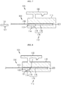
- FIG. 1 is a schematic sectional view showing a conventional FPCB connector.
- a FPCB 1 is coupled to a connector 2 by means of soldering 3.
- the flatness of the FPCB 1 must be considered for the soldering 3, and a reinforcing plate is required, which results in complicated processes and high cost.
- productivity is deteriorated due to high soldering defect rate.
- the present disclosure is directed to providing a FPCB connector where a FPCB may be coupled to a connector without soldering, and a battery module and a battery pack including the FPCB connector.
- a FPCB connector comprising: a first main body to which a first FPCB is coupled; and a second main body to which a second FPCB is coupled, the second main body being coupled to the first main body to be electrically connected thereto, wherein at least one of the first main body and the second main body is coupled to the first FPCB or the second FPCB without soldering.
- the first main body may include a first body having an insert groove into which the first FPCB is inserted; and a first fixing portion coupled to the first body into which the first FPCB is inserted to fix the first FPCB.
- a stepped portion formed by a height difference may be formed at a bottom of the first body, and the first FPCB may be located at one side of the stepped portion to contact one side of the stepped portion or be spaced apart from one side of the stepped portion.
- the stepped portion may include a high surface having a great height; and a low surface having a relatively smaller height compared to the high surface
- the first FPCB may have a first body portion and a first end portion so that the first end portion of the first FPCB is thicker than the first body portion of the first FPCB, the first end portion of the first FPCB having a greater thickness may be in contact with the high surface of the stepped portion or is spaced apart from the high surface of the stepped portion, a preset space may be formed between the low surface of the stepped portion and the first body portion of the first FPCB, and the first fixing portion may be inserted into the space and coupled to the first body to come into contact with the first body portion of the first FPCB.
- a coupling groove may be formed at an upper surface of the second main body, and a coupling protrusion coupled to the coupling groove may be formed at an upper side of the first main body so that the first main body and the second main body are coupled to each other.
- the second main body may include a second body having an open portion formed at one side thereof so that the second FPCB is inserted therein; a terminal member coupled to the second body and configured to electrically connect the first FPCB and the second FPCB when the first main body is coupled to the second main body; and a second fixing portion coupled to the second body through the open portion of the second body into which the second FPCB is inserted to fix the second FPCB.
- the second body may include a first extension configured to extend from one side of the second main body; and a second extension configured to extend from the other side of the second main body to be located opposite to the first extension, and the second FPCB may be inserted between the first extension and the second extension.
- the second extension may be provided in plural so that the plurality of second extensions are arranged at preset intervals
- the terminal member may be provided in plural so that the plurality of terminal members are disposed between the second extensions, respectively.
- a contact portion may be formed at the second fixing portion to contact the second FPCB, and at least one of the plurality of terminal members may be interposed between the contact portion and the second extension.
- the second FPCB may have a second body portion and a second end portion so that the second end portion of the second FPCB is formed wider than the second body portion of the second FPCB, and the second fixing portion may have catching portions extending inward from both end portions thereof so that the second end portion of the second FPCB is caught by the catching portions.
- a battery module comprising the FPCB connector described above
- a battery pack comprising the FPCB connector described above.
- a FPCB may be coupled to a connector without soldering.
- 'combine' or 'connect' may refer not only to a case where one member and another member are directly combined or directly connected but also a case where one member is indirectly combined with another member via a connecting member or is indirectly connected.
- a FPCB refers to a flexible printed circuit board
- soldering refers to lead soldering.
- a fixing portion refers to a concept that includes all of a case where the fixing portion is in close contact with the FPCB without any space therebetween to completely block the movement of the FPCB and a case where the FPCB is caught by the fixing portion not to be separated from a main body even though there is a slight gap.
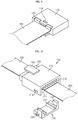
- FIG. 2 is an exploded perspective view showing a FPCB connector according to the first embodiment of the present disclosure
- FIG. 3 is a perspective view showing that a FPCB is coupled to a main body of a connector, in the FPCB connector according to the first embodiment of the present disclosure
- FIG. 4 is a perspective view showing that a first main body of the connector coupled to a first FPCB and a second main body of the connector coupled to a second FPCB are coupled to each other, in the FPCB connector according to the first embodiment of the present disclosure
- FIG. 5 is a sectional view of FIG. 4
- FIG. 6 is an exploded sectional view showing the first main body of the FPCB connector according to the first embodiment of the present disclosure
- FIG. 7 is a sectional view of FIG.
- FIG. 6 showing that the first FPCB is inserted into an insert groove of a first body of the first main body
- FIG. 8 is a sectional view of FIG. 7 showing that a first fixing portion is fixed to the first body of the first main body to fix the first FPCB
- FIG. 9 is a perspective view showing the first main body of FIG. 3 in a vertically reversed state
- FIG. 10 is a perspective view showing that a second fixing portion is separated from a second body of the second main body of the FPCB connector according to the first embodiment of the present disclosure
- FIG. 11 is a perspective view of FIG. 10 showing that the second fixing portion is coupled to the second body of the second main body
- FIG. 12 is a sectional view, taken along an arrow A of FIG. 11
- FIG. 13 is a sectional view, taken along an arrow B-B' of FIG. 11 .
- a FPCB connector 10 includes a first main body 100 and a second main body 200. Also, a first FPCB 300 may be coupled to the first main body 100 without soldering, and a second FPCB 400 may be coupled to the second main body 200 without soldering.
- first FPCB may be connected to the first main body 100 without soldering, or only the second FPCB may be connected to the second main body 200 without soldering.
- both of the first FPCB 300 and the second FPCB 400 may be coupled to the first main body 100 and the second main body 200 without soldering, respectively.
- first main body 100 and the second main body 200 may be any of a female connector and a male connector, but hereinafter, for convenience of explanation, it will be described that the first main body 100 is a female connector and the second main body 200 is a male connector.
- the scope of the present disclosure is not limited thereto.
- the first FPCB 300 may be coupled to the first main body 100. As described above, the first FPCB 300 is coupled to the first main body 100 without soldering. To this end, the first main body 100 may include a first body 110 and a first fixing portion 120.
- an insert groove 111 is formed at the first body 110 so that the first FPCB 300 is inserted therein, and as shown in FIG. 3 , the first FPCB 300 is inserted into the insert groove 111 of the first body 110.
- the first fixing portion 120 is coupled to the first body 110 into which the first FPCB 300 is inserted to fix the first FPCB 300.
- a hooking groove 114 may be formed at the first body 110, a hooking protrusion 121 may be formed at the first fixing portion 120, and the hooking protrusion 121 of the first fixing portion 120 may be fastened to the hooking groove 114 of the first body 110 so that the first fixing portion 120 is coupled to the first body 110.
- this coupling method is only an example.
- the first fixing portion 120 may be in contact with at least a portion of the first FPCB 300, and the first FPCB 300 is caught by a hooking point P of the first fixing portion 120 so as not to be separated from the first body 110. In this way, the first FPCB 300 may be coupled to the first main body 100 without soldering.
- a stepped portion 116 formed by a height difference may be formed at a bottom 112 of the first body 110.
- the stepped portion 116 includes a high surface 118 and a low surface 119.
- the high surface 118 refers to a surface with a relatively great height compared to the low surface 119
- the low surface 119 refers to a surface with a relatively small height compared to the high surface 118.
- the first FPCB 300 may include a first body portion 310 and a first end portion 320, and in this case, the first end portion 320 of the first FPCB 300 may be formed thicker than the first body portion 310 of the first FPCB 300.
- the first FPCB 300 may be located at one side of the stepped portion 116 to contact one side of the stepped portion 116 or to be spaced apart from one side of the stepped portion 116.
- the first end portion 320 of the first FPCB 300 formed thickly may contact the high surface 118 of the stepped portion 116, or alternatively, the first end portion 320 of the first FPCB 300 may be spaced apart from the high surface 118 of the stepped portion 116.
- the first fixing portion 120 contacts the first body portion 310 of the first FPCB 300 to support the first body portion 310, the first end portion 320 of the first FPCB 300 may be spaced apart from the high surface 118 of the stepped portion 116.
- a preset space 113 is formed between the low surface 119 of the stepped portion 116 and the first body portion 310 of the first FPCB 300.
- the first fixing portion 120 if the first fixing portion 120 is inserted into the space 113 formed between the low surface 119 of the stepped portion 116 and the first body portion 310 of the first FPCB 300 and is coupled to the first body 110, the first fixing portion 120 contacts the first body portion 310 of the first FPCB 300 to support the first FPCB 300. At this time, the hooking protrusion 121 of the first fixing portion 120 may be fastened to the hooking groove 114 of the first body 110.
- the first fixing portion 120 does not need to press the first body portion 310 of the first FPCB 300. This is because, if the first fixing portion 120 presses the first body portion 310 of the first FPCB 300 too hard, the first FPCB 300 may be damaged. Accordingly, the first fixing portion 120 may be configured to simply contact the first body portion 310 of the first FPCB 300 so as to support the first FPCB 300.
- the first fixing portion 120 comes into contact with the first body portion 310 of the first FPCB 300, the first end portion 320 of the first FPCB 300 formed thickly is caught at the hooking point P of the first fixing portion 120 is prevented from being separated from the first body 110. That is, even if the first FPCB 300 is pulled back, the first FPCB 300 does not fall out of the first main body 100. Accordingly, the first FPCB 300 may be coupled to the first main body 100 without soldering.
- the second FPCB 400 is coupled to the second main body 200, and the second main body 200 is coupled to be electrically connected to the first main body 100.
- the first main body 100 and the second main body 200 may be coupled in various ways.
- a coupling groove 240 may be formed at an upper surface of the second main body 200
- a coupling protrusion 130 may be formed at an upper side of the first main body 100 so as to be coupled to the coupling groove 240
- the coupling protrusion 130 of the first main body 100 may be fastened to the coupling groove 240 of the second main body 200 so that the first main body 100 and the second main body 200 are coupled to each other.
- the first main body 100 and the second main body 200 may be coupled in more diverse ways, and is not limited to the above coupling method.
- the second FPCB 400 is coupled to the second main body 200 without soldering.
- the second main body 200 may include a second body 210, a terminal member 220 (see FIG. 5 ), and a second fixing portion 230.
- the second body 210 may have an open portion 211 formed to open one side thereof, and the second FPCB 400 is inserted into the second body 210 through the open portion 211.
- the terminal member 220 is coupled to the second body 210. In addition, if the first main body 100 is coupled to the second main body 200, the terminal member 220 electrically connects the first FPCB 300 and the second FPCB 400.
- the terminal member 220 may be formed in various shapes.
- the terminal member 220 may be shaped as shown in FIG. 5 to contact both the first FPCB 300 and the second FPCB 400.
- the shape of the terminal member 220 is not limited to FIG. 5 .
- the terminal member 220 may be made of various electrically conductive materials.
- the terminal member 220 may be made of copper.
- the second fixing portion 230 is coupled to the second body 210 through the open portion 211 of the second body 210 into which the second FPCB 400 is inserted to fix the second FPCB 400.
- the second body 210 may have a first extension 212 and a second extension 213.
- the first extension 212 may be configured to extend from one side of the second body 210 of the second main body 200, for example from an upper side of the second body 210 based on FIG. 12 .
- the second extension 213 may be configured to extend from the other side of the second body 210 of the second main body 200, for example from a lower side of the second body 210 based on FIG. 12 , to be located opposite to the first extension 212.
- the second FPCB 400 is inserted and supported between the first extension 212 and the second extension 213.
- the second extension 213 may be provided in plural, and the plurality of second extensions 213 may be arranged at preset intervals.
- the first extension 212 may also be provided in plural, and the plurality of first extensions 212 may be arranged at the same interval as the second extensions 213.
- the first extension 212 and the second extension 213 may be disposed to face each other vertically.
- the terminal member 220 may be provided in plural, and the plurality of terminal members 220 may be disposed between the second extensions 213, respectively.
- a contact portion 231 may be formed at the second fixing portion 230 to contact the second FPCB 400, and the contact portion 231 of the second fixing portion 230 is in contact with the second FPCB 400 to support the second FPCB 400.
- at least one of the plurality of terminal members 220 may be configured to be interposed between the contact portion 231 and the second extension 213.
- the second FPCB 400 may include a second body portion 410 and a second end portion 420, and the second end portion 420 of the second FPCB 400 may be formed wider than the second body portion 410 of the second FPCB 400.
- the second fixing portion 230 may have catching portions 232 formed to extend inward from both end portions thereof, and the second end portion 420 of the second FPCB 400 having a greater width is caught by the catching portions 232 of the second fixing portion 230 and is thus prevented from being separated from the second body 210. That is, even if the second FPCB 400 is pulled downward based on FIG. 13 , the second end portion 420 is caught by the catching portion 232 and thus the second FPCB 400 is not pulled out of the second body 210. Accordingly, the second FPCB 400 may be coupled to the second main body 200 without soldering.
- the second fixing portion 230 is coupled to the second body 210 from a lower side.
- a hooking groove 214 may be formed at the second body 210
- a hooking protrusion 233 may be formed at the second fixing portion 230
- the hooking protrusion 233 of the second fixing portion 230 may be fastened to the hooking groove 214 of the second body 210 so that the second fixing portion 230 is coupled to the second body 210.
- this coupling method is only an example.
- FIG. 6 shows a state before the first FPCB 300 is inserted into the insert groove 111 of the first body 110 of the first main body 100.
- the stepped portion 116 is formed at the bottom 112 of the first body 110 due to a height difference.
- the preset space 113 is formed between the low surface 119 of the stepped portion 116 and the first body portion 310 of the first FPCB 300.
- the first fixing portion 120 is inserted into the space 113 formed between the low surface 119 of the stepped portion 116 and the first body portion 310 of the first FPCB 300 and is coupled to the first body 110, whereby the first fixing portion 120 comes into contact with the first body portion 310 of the first FPCB 300 to support the first FPCB 300. If the first fixing portion 120 comes into contact with the first FPCB 300 in this way, the first end portion 320 of the first FPCB 300 having a greater thickness is caught by the hooking point P of the first fixing portion 120 and is thus prevented from being separated from the first body 110. Accordingly, the first FPCB 300 may be coupled to the first main body 100 without soldering.
- the second FPCB 400 is inserted into the second body 210 through the open portion 211 formed at the second body 210, and referring to FIG. 11 , the second fixing portion 230 is coupled to the second body 210 through the open portion 211 of the second body 210 into which the second FPCB 400 is inserted to fix the second FPCB 400.
- the second end portion 420 of the second FPCB 400 having a greater width is caught by the catching portion 232 of the second fixing portion 230 and is thus prevented from being separated from the second body 210. Accordingly, the second FPCB 400 may be coupled to the second main body 200 without soldering.
- the terminal member 220 comes into contact with both the first FPCB 300 and the second FPCB 400, so that the first FPCB 300 and the second The FPCB 400 are electrically connected.
- FIG. 14 is a sectional view showing that the first main body of the connector coupled to the first FPCB and the second main body of the connector coupled to the second FPCB are coupled to each other, in a FPCB connector according to the second embodiment of the present disclosure.
- the stepped portion 116 is not formed at the bottom 112 of the first body 110 of the first main body 100, and the first body portion 310 and the first end portion 320 are formed with the same thickness, different from the first embodiment.
- a battery module (not shown) according to an embodiment of the present disclosure may include at least one FPCB connector 10 as described above.
- the battery module (not shown) includes a battery cell stack, and the FPCB connector 10 according to an embodiment of the present disclosure may be used for electrical connection to sense temperature or the like of a battery cell.
- the use of the FPCB connector 10 is not limited to sensing.
- a battery pack may include one or more battery modules (not shown) as described above.
- the battery pack may further includes a case for accommodating the battery modules (not shown), and various devices for controlling charge and discharge of the battery modules (not shown), such as a BMS, a current sensor, a fuse, and the like.
- the FPCB connector 10 according to an embodiment of the present disclosure may be used to connect LV wires (Low Voltage Wires) used in a battery pack (not shown) to each other.
- LV wires Low Voltage Wires
- the use of the FPCB connector 10 is not limited to LV wires.
- the present disclosure relates to a FPCB connector, and a battery module and a battery pack including the FPCB connector, and may be used in industries related to batteries.
Landscapes
- Engineering & Computer Science (AREA)
- Chemical & Material Sciences (AREA)
- Chemical Kinetics & Catalysis (AREA)
- Electrochemistry (AREA)
- General Chemical & Material Sciences (AREA)
- Microelectronics & Electronic Packaging (AREA)
- Manufacturing & Machinery (AREA)
- Coupling Device And Connection With Printed Circuit (AREA)
- Battery Mounting, Suspending (AREA)
Abstract
Description
- The present application claims priority to
Korean Patent Application No. 10-2019-0101973 filed on August 20, 2019 - The present disclosure relates to a FPCB connector, and a battery module and a battery pack including the FPCB connector, and more particular, to a FPCB connector where a FPCB may be coupled to a connector without soldering, and a battery module and a battery pack including the FPCB connector.
- In general, a connector is used in various electronic devices for signal transmission and power supply with various additional devices. For example, a connector for connecting FPCBs is used for charging and discharging a secondary battery product, including electronic devices such as laptops, tablet PCs, and smart phones.
-
FIG. 1 is a schematic sectional view showing a conventional FPCB connector. Referring toFIG. 1 , a FPCB 1 is coupled to aconnector 2 by means of soldering 3. However, in the conventional art where the FPCB 1 is coupled to theconnector 2 by soldering 3, the flatness of the FPCB 1 must be considered for the soldering 3, and a reinforcing plate is required, which results in complicated processes and high cost. In addition, productivity is deteriorated due to high soldering defect rate. - The present disclosure is directed to providing a FPCB connector where a FPCB may be coupled to a connector without soldering, and a battery module and a battery pack including the FPCB connector.
- In one aspect of the present disclosure, there is provided a FPCB connector, comprising: a first main body to which a first FPCB is coupled; and a second main body to which a second FPCB is coupled, the second main body being coupled to the first main body to be electrically connected thereto, wherein at least one of the first main body and the second main body is coupled to the first FPCB or the second FPCB without soldering.
- Also, the first main body may include a first body having an insert groove into which the first FPCB is inserted; and a first fixing portion coupled to the first body into which the first FPCB is inserted to fix the first FPCB.
- In addition, a stepped portion formed by a height difference may be formed at a bottom of the first body, and the first FPCB may be located at one side of the stepped portion to contact one side of the stepped portion or be spaced apart from one side of the stepped portion.
- Also, the stepped portion may include a high surface having a great height; and a low surface having a relatively smaller height compared to the high surface, the first FPCB may have a first body portion and a first end portion so that the first end portion of the first FPCB is thicker than the first body portion of the first FPCB, the first end portion of the first FPCB having a greater thickness may be in contact with the high surface of the stepped portion or is spaced apart from the high surface of the stepped portion, a preset space may be formed between the low surface of the stepped portion and the first body portion of the first FPCB, and the first fixing portion may be inserted into the space and coupled to the first body to come into contact with the first body portion of the first FPCB.
- In addition, a coupling groove may be formed at an upper surface of the second main body, and a coupling protrusion coupled to the coupling groove may be formed at an upper side of the first main body so that the first main body and the second main body are coupled to each other.
- Also, the second main body may include a second body having an open portion formed at one side thereof so that the second FPCB is inserted therein; a terminal member coupled to the second body and configured to electrically connect the first FPCB and the second FPCB when the first main body is coupled to the second main body; and a second fixing portion coupled to the second body through the open portion of the second body into which the second FPCB is inserted to fix the second FPCB.
- In addition, the second body may include a first extension configured to extend from one side of the second main body; and a second extension configured to extend from the other side of the second main body to be located opposite to the first extension, and the second FPCB may be inserted between the first extension and the second extension.
- Also, the second extension may be provided in plural so that the plurality of second extensions are arranged at preset intervals, and the terminal member may be provided in plural so that the plurality of terminal members are disposed between the second extensions, respectively.
- In addition, a contact portion may be formed at the second fixing portion to contact the second FPCB, and at least one of the plurality of terminal members may be interposed between the contact portion and the second extension.
- Also, the second FPCB may have a second body portion and a second end portion so that the second end portion of the second FPCB is formed wider than the second body portion of the second FPCB, and the second fixing portion may have catching portions extending inward from both end portions thereof so that the second end portion of the second FPCB is caught by the catching portions.
- Meanwhile, in another aspect of the present disclosure, there is provided a battery module, comprising the FPCB connector described above, and there is also provided a battery pack, comprising the FPCB connector described above.
- According to the embodiments of the present disclosure, a FPCB may be coupled to a connector without soldering.
- In addition, since the process is simplified, manufacturing is simplified, and the defect rate is reduced, thereby improving productivity.
-
-
FIG. 1 is a schematic sectional view showing a conventional FPCB connector. -
FIG. 2 is an exploded perspective view showing a FPCB connector according to the first embodiment of the present disclosure. -
FIG. 3 is a perspective view showing that a FPCB is coupled to a main body of a connector, in the FPCB connector according to the first embodiment of the present disclosure. -
FIG. 4 is a perspective view showing that a first main body of the connector coupled to a first FPCB and a second main body of the connector coupled to a second FPCB are coupled to each other, in the FPCB connector according to the first embodiment of the present disclosure. -
FIG. 5 is a sectional view ofFIG. 4 . -
FIG. 6 is an exploded sectional view showing the first main body of the FPCB connector according to the first embodiment of the present disclosure. -
FIG. 7 is a sectional view ofFIG. 6 showing that the first FPCB is inserted into an insert groove of a first body of the first main body. -
FIG. 8 is a sectional view ofFIG. 7 showing that a first fixing portion is fixed to the first body of the first main body to fix the first FPCB. -
FIG. 9 is a perspective view showing the first main body ofFIG. 3 in a vertically reversed state. -
FIG. 10 is a perspective view showing that a second fixing portion is separated from a second body of the second main body of the FPCB connector according to the first embodiment of the present disclosure. -
FIG. 11 is a perspective view ofFIG. 10 showing that the second fixing portion is coupled to the second body of the second main body. -
FIG. 12 is a sectional view, taken along an arrow A ofFIG. 11 . -
FIG. 13 is a sectional view, taken along an arrow B-B' ofFIG. 11 . -
FIG. 14 is a sectional view showing that the first main body of the connector coupled to the first FPCB and the second main body of the connector coupled to the second FPCB are coupled to each other, in a FPCB connector according to the second embodiment of the present disclosure. - Hereinafter, preferred embodiments of the present disclosure will be described in detail with reference to the accompanying drawings. Prior to the description, it should be understood that the terms used in the specification and the appended claims should not be construed as limited to general and dictionary meanings, but interpreted based on the meanings and concepts corresponding to technical aspects of the present disclosure on the basis of the principle that the inventor is allowed to define terms appropriately for the best explanation. Therefore, the description proposed herein is just a preferable example for the purpose of illustrations only, not intended to limit the scope of the disclosure, so it should be understood that other equivalents and modifications could be made thereto without departing from the scope of the disclosure.
- In the drawings, the size of each element or a specific part of the element may be exaggerated, omitted, or schematically illustrated for convenience and clarity of a description. Thus, the size of each element does not entirely reflect the actual size of the element. A detailed description of well-known functions or elements associated with the present disclosure will be omitted if it unnecessarily obscures the subject matter of the present disclosure.
- The term, 'combine' or 'connect' as used herein, may refer not only to a case where one member and another member are directly combined or directly connected but also a case where one member is indirectly combined with another member via a connecting member or is indirectly connected.
- In this specification, a FPCB refers to a flexible printed circuit board, and soldering refers to lead soldering. In addition, in this specification, it should be noted that a fixing portion refers to a concept that includes all of a case where the fixing portion is in close contact with the FPCB without any space therebetween to completely block the movement of the FPCB and a case where the FPCB is caught by the fixing portion not to be separated from a main body even though there is a slight gap.
-
FIG. 2 is an exploded perspective view showing a FPCB connector according to the first embodiment of the present disclosure,FIG. 3 is a perspective view showing that a FPCB is coupled to a main body of a connector, in the FPCB connector according to the first embodiment of the present disclosure,FIG. 4 is a perspective view showing that a first main body of the connector coupled to a first FPCB and a second main body of the connector coupled to a second FPCB are coupled to each other, in the FPCB connector according to the first embodiment of the present disclosure,FIG. 5 is a sectional view ofFIG. 4 ,FIG. 6 is an exploded sectional view showing the first main body of the FPCB connector according to the first embodiment of the present disclosure,FIG. 7 is a sectional view ofFIG. 6 showing that the first FPCB is inserted into an insert groove of a first body of the first main body,FIG. 8 is a sectional view ofFIG. 7 showing that a first fixing portion is fixed to the first body of the first main body to fix the first FPCB,FIG. 9 is a perspective view showing the first main body ofFIG. 3 in a vertically reversed state,FIG. 10 is a perspective view showing that a second fixing portion is separated from a second body of the second main body of the FPCB connector according to the first embodiment of the present disclosure,FIG. 11 is a perspective view ofFIG. 10 showing that the second fixing portion is coupled to the second body of the second main body,FIG. 12 is a sectional view, taken along an arrow A ofFIG. 11 , andFIG. 13 is a sectional view, taken along an arrow B-B' ofFIG. 11 . - Referring to
FIG. 2 , aFPCB connector 10 according to the first embodiment of the present disclosure includes a firstmain body 100 and a secondmain body 200. Also, a first FPCB 300 may be coupled to the firstmain body 100 without soldering, and a second FPCB 400 may be coupled to the secondmain body 200 without soldering. - Here, only the first FPCB may be connected to the first
main body 100 without soldering, or only the second FPCB may be connected to the secondmain body 200 without soldering. Alternatively, both of the first FPCB 300 and the second FPCB 400 may be coupled to the firstmain body 100 and the secondmain body 200 without soldering, respectively. - Meanwhile, the first
main body 100 and the secondmain body 200 may be any of a female connector and a male connector, but hereinafter, for convenience of explanation, it will be described that the firstmain body 100 is a female connector and the secondmain body 200 is a male connector. However, the scope of the present disclosure is not limited thereto. - The first FPCB 300 may be coupled to the first
main body 100. As described above, the first FPCB 300 is coupled to the firstmain body 100 without soldering. To this end, the firstmain body 100 may include afirst body 110 and afirst fixing portion 120. - Referring to
FIG. 2 , aninsert groove 111 is formed at thefirst body 110 so that the first FPCB 300 is inserted therein, and as shown inFIG. 3 , the first FPCB 300 is inserted into theinsert groove 111 of thefirst body 110. Referring toFIGS. 3, 4 and9 together, thefirst fixing portion 120 is coupled to thefirst body 110 into which the first FPCB 300 is inserted to fix the first FPCB 300. - Referring to
FIGS. 5 to 9 , ahooking groove 114 may be formed at thefirst body 110, a hookingprotrusion 121 may be formed at thefirst fixing portion 120, and thehooking protrusion 121 of thefirst fixing portion 120 may be fastened to thehooking groove 114 of thefirst body 110 so that thefirst fixing portion 120 is coupled to thefirst body 110. However, this coupling method is only an example. - Here, referring to
FIG. 5 , thefirst fixing portion 120 may be in contact with at least a portion of thefirst FPCB 300, and thefirst FPCB 300 is caught by a hooking point P of thefirst fixing portion 120 so as not to be separated from thefirst body 110. In this way, thefirst FPCB 300 may be coupled to the firstmain body 100 without soldering. - Specifically, referring to
FIG. 6 , a steppedportion 116 formed by a height difference may be formed at a bottom 112 of thefirst body 110. The steppedportion 116 includes ahigh surface 118 and alow surface 119. Also, thehigh surface 118 refers to a surface with a relatively great height compared to thelow surface 119, and thelow surface 119 refers to a surface with a relatively small height compared to thehigh surface 118. - Based on
FIG. 6 , a right side of thefirst body 110 is thehigh surface 118, and a left side is thelow surface 119. Thefirst FPCB 300 may include afirst body portion 310 and afirst end portion 320, and in this case, thefirst end portion 320 of thefirst FPCB 300 may be formed thicker than thefirst body portion 310 of thefirst FPCB 300. - Here, the
first FPCB 300 may be located at one side of the steppedportion 116 to contact one side of the steppedportion 116 or to be spaced apart from one side of the steppedportion 116. For example, referring toFIG. 7 in which thefirst FPCB 300 is inserted into theinsert groove 111 of thefirst body 110 of the firstmain body 100, thefirst end portion 320 of thefirst FPCB 300 formed thickly may contact thehigh surface 118 of the steppedportion 116, or alternatively, thefirst end portion 320 of thefirst FPCB 300 may be spaced apart from thehigh surface 118 of the steppedportion 116. - Since the
first fixing portion 120, explained later, contacts thefirst body portion 310 of thefirst FPCB 300 to support thefirst body portion 310, thefirst end portion 320 of thefirst FPCB 300 may be spaced apart from thehigh surface 118 of the steppedportion 116. - In addition, referring to
FIG. 7 , if thefirst FPCB 300 is inserted into theinsert groove 111 of thefirst body 110 of the first main body 100 (seeFIG. 6 ), apreset space 113 is formed between thelow surface 119 of the steppedportion 116 and thefirst body portion 310 of thefirst FPCB 300. - In addition, as shown in
FIG. 8 , if thefirst fixing portion 120 is inserted into thespace 113 formed between thelow surface 119 of the steppedportion 116 and thefirst body portion 310 of thefirst FPCB 300 and is coupled to thefirst body 110, thefirst fixing portion 120 contacts thefirst body portion 310 of thefirst FPCB 300 to support thefirst FPCB 300. At this time, the hookingprotrusion 121 of thefirst fixing portion 120 may be fastened to the hookinggroove 114 of thefirst body 110. - Here, the
first fixing portion 120 does not need to press thefirst body portion 310 of thefirst FPCB 300. This is because, if thefirst fixing portion 120 presses thefirst body portion 310 of thefirst FPCB 300 too hard, thefirst FPCB 300 may be damaged. Accordingly, thefirst fixing portion 120 may be configured to simply contact thefirst body portion 310 of thefirst FPCB 300 so as to support thefirst FPCB 300. - As shown in
FIG. 8 , if thefirst fixing portion 120 comes into contact with thefirst body portion 310 of thefirst FPCB 300, thefirst end portion 320 of thefirst FPCB 300 formed thickly is caught at the hooking point P of thefirst fixing portion 120 is prevented from being separated from thefirst body 110. That is, even if thefirst FPCB 300 is pulled back, thefirst FPCB 300 does not fall out of the firstmain body 100. Accordingly, thefirst FPCB 300 may be coupled to the firstmain body 100 without soldering. - The
second FPCB 400 is coupled to the secondmain body 200, and the secondmain body 200 is coupled to be electrically connected to the firstmain body 100. - The first
main body 100 and the secondmain body 200 may be coupled in various ways. For example, referring toFIG. 2 , acoupling groove 240 may be formed at an upper surface of the secondmain body 200, acoupling protrusion 130 may be formed at an upper side of the firstmain body 100 so as to be coupled to thecoupling groove 240, and thecoupling protrusion 130 of the firstmain body 100 may be fastened to thecoupling groove 240 of the secondmain body 200 so that the firstmain body 100 and the secondmain body 200 are coupled to each other. However, the firstmain body 100 and the secondmain body 200 may be coupled in more diverse ways, and is not limited to the above coupling method. - In addition, as described above, the
second FPCB 400 is coupled to the secondmain body 200 without soldering. To this end, the secondmain body 200 may include asecond body 210, a terminal member 220 (seeFIG. 5 ), and asecond fixing portion 230. - Referring to
FIG. 10 , thesecond body 210 may have anopen portion 211 formed to open one side thereof, and thesecond FPCB 400 is inserted into thesecond body 210 through theopen portion 211. - The
terminal member 220 is coupled to thesecond body 210. In addition, if the firstmain body 100 is coupled to the secondmain body 200, theterminal member 220 electrically connects thefirst FPCB 300 and thesecond FPCB 400. Theterminal member 220 may be formed in various shapes. - For example, the
terminal member 220 may be shaped as shown inFIG. 5 to contact both thefirst FPCB 300 and thesecond FPCB 400. However, the shape of theterminal member 220 is not limited toFIG. 5 . In addition, theterminal member 220 may be made of various electrically conductive materials. For example, theterminal member 220 may be made of copper. - Referring to
FIG. 11 , thesecond fixing portion 230 is coupled to thesecond body 210 through theopen portion 211 of thesecond body 210 into which thesecond FPCB 400 is inserted to fix thesecond FPCB 400. - Referring to
FIG. 12 , thesecond body 210 may have afirst extension 212 and asecond extension 213. Thefirst extension 212 may be configured to extend from one side of thesecond body 210 of the secondmain body 200, for example from an upper side of thesecond body 210 based onFIG. 12 . In addition, thesecond extension 213 may be configured to extend from the other side of thesecond body 210 of the secondmain body 200, for example from a lower side of thesecond body 210 based onFIG. 12 , to be located opposite to thefirst extension 212. - In addition, as shown in
FIG. 12 , thesecond FPCB 400 is inserted and supported between thefirst extension 212 and thesecond extension 213. Here, thesecond extension 213 may be provided in plural, and the plurality ofsecond extensions 213 may be arranged at preset intervals. - The
first extension 212 may also be provided in plural, and the plurality offirst extensions 212 may be arranged at the same interval as thesecond extensions 213. Thefirst extension 212 and thesecond extension 213 may be disposed to face each other vertically. In addition, theterminal member 220 may be provided in plural, and the plurality ofterminal members 220 may be disposed between thesecond extensions 213, respectively. - Here, referring to
FIGS. 11 and 12 , acontact portion 231 may be formed at thesecond fixing portion 230 to contact thesecond FPCB 400, and thecontact portion 231 of thesecond fixing portion 230 is in contact with thesecond FPCB 400 to support thesecond FPCB 400. In addition, at least one of the plurality ofterminal members 220 may be configured to be interposed between thecontact portion 231 and thesecond extension 213. - Referring to
FIGS. 2 and13 , thesecond FPCB 400 may include asecond body portion 410 and asecond end portion 420, and thesecond end portion 420 of thesecond FPCB 400 may be formed wider than thesecond body portion 410 of thesecond FPCB 400. - In addition, as shown in
FIG. 13 , thesecond fixing portion 230 may have catchingportions 232 formed to extend inward from both end portions thereof, and thesecond end portion 420 of thesecond FPCB 400 having a greater width is caught by the catchingportions 232 of thesecond fixing portion 230 and is thus prevented from being separated from thesecond body 210. That is, even if thesecond FPCB 400 is pulled downward based onFIG. 13 , thesecond end portion 420 is caught by the catchingportion 232 and thus thesecond FPCB 400 is not pulled out of thesecond body 210. Accordingly, thesecond FPCB 400 may be coupled to the secondmain body 200 without soldering. - Referring to
FIGS. 10 and11 , after thesecond FPCB 400 is inserted into thesecond body 210 through theopen portion 211, thesecond fixing portion 230 is coupled to thesecond body 210 from a lower side. Here, a hookinggroove 214 may be formed at thesecond body 210, a hookingprotrusion 233 may be formed at thesecond fixing portion 230, and the hookingprotrusion 233 of thesecond fixing portion 230 may be fastened to the hookinggroove 214 of thesecond body 210 so that thesecond fixing portion 230 is coupled to thesecond body 210. However, this coupling method is only an example. - Hereinafter, operations and effects of the
FPCB connector 10 according to the first embodiment of the present disclosure will be described with reference to the drawings. -
FIG. 6 shows a state before thefirst FPCB 300 is inserted into theinsert groove 111 of thefirst body 110 of the firstmain body 100. Here, the steppedportion 116 is formed at the bottom 112 of thefirst body 110 due to a height difference. Referring toFIG. 7 , if thefirst FPCB 300 is inserted into theinsert groove 111 of thefirst body 110 of the firstmain body 100, thepreset space 113 is formed between thelow surface 119 of the steppedportion 116 and thefirst body portion 310 of thefirst FPCB 300. In addition, referring toFIG. 8 , thefirst fixing portion 120 is inserted into thespace 113 formed between thelow surface 119 of the steppedportion 116 and thefirst body portion 310 of thefirst FPCB 300 and is coupled to thefirst body 110, whereby thefirst fixing portion 120 comes into contact with thefirst body portion 310 of thefirst FPCB 300 to support thefirst FPCB 300. If thefirst fixing portion 120 comes into contact with thefirst FPCB 300 in this way, thefirst end portion 320 of thefirst FPCB 300 having a greater thickness is caught by the hooking point P of thefirst fixing portion 120 and is thus prevented from being separated from thefirst body 110. Accordingly, thefirst FPCB 300 may be coupled to the firstmain body 100 without soldering. - In addition, referring to
FIG. 10 , thesecond FPCB 400 is inserted into thesecond body 210 through theopen portion 211 formed at thesecond body 210, and referring toFIG. 11 , thesecond fixing portion 230 is coupled to thesecond body 210 through theopen portion 211 of thesecond body 210 into which thesecond FPCB 400 is inserted to fix thesecond FPCB 400. In addition, as shown inFIG. 13 , thesecond end portion 420 of thesecond FPCB 400 having a greater width is caught by the catchingportion 232 of thesecond fixing portion 230 and is thus prevented from being separated from thesecond body 210. Accordingly, thesecond FPCB 400 may be coupled to the secondmain body 200 without soldering. - In addition, as shown in
FIGS. 3 and 4 , if the firstmain body 100 and the secondmain body 200 are coupled, as inFIG. 5 , theterminal member 220 comes into contact with both thefirst FPCB 300 and thesecond FPCB 400, so that thefirst FPCB 300 and the second TheFPCB 400 are electrically connected. -
FIG. 14 is a sectional view showing that the first main body of the connector coupled to the first FPCB and the second main body of the connector coupled to the second FPCB are coupled to each other, in a FPCB connector according to the second embodiment of the present disclosure. - Hereinafter, the operations and effects of the
FPCB connector 10 according to the second embodiment of the present disclosure will be described with reference to the accompanying drawings. Here, a feature already explained in relation to theFPCB connector 10 according to the first disclosure of the present disclosure will not be described in detail again. - Referring to
FIG. 14 , in the second embodiment of the present disclosure, the steppedportion 116 is not formed at the bottom 112 of thefirst body 110 of the firstmain body 100, and thefirst body portion 310 and thefirst end portion 320 are formed with the same thickness, different from the first embodiment. - Meanwhile, a battery module (not shown) according to an embodiment of the present disclosure may include at least one
FPCB connector 10 as described above. The battery module (not shown) includes a battery cell stack, and theFPCB connector 10 according to an embodiment of the present disclosure may be used for electrical connection to sense temperature or the like of a battery cell. However, the use of theFPCB connector 10 is not limited to sensing. - Meanwhile, a battery pack (not shown) according to an embodiment of the present disclosure, may include one or more battery modules (not shown) as described above. Also, in addition to the battery modules (not shown), the battery pack (not shown) may further includes a case for accommodating the battery modules (not shown), and various devices for controlling charge and discharge of the battery modules (not shown), such as a BMS, a current sensor, a fuse, and the like. In addition, the
FPCB connector 10 according to an embodiment of the present disclosure may be used to connect LV wires (Low Voltage Wires) used in a battery pack (not shown) to each other. However, the use of theFPCB connector 10 is not limited to LV wires. - The present disclosure has been described in detail. However, it should be understood that the detailed description and specific examples, while indicating preferred embodiments of the disclosure, are given by way of illustration only, since various changes and modifications within the scope of the disclosure will become apparent to those skilled in the art from this detailed description.
- The present disclosure relates to a FPCB connector, and a battery module and a battery pack including the FPCB connector, and may be used in industries related to batteries.
Claims (12)
- A FPCB connector, comprising:a first main body to which a first FPCB is coupled; anda second main body to which a second FPCB is coupled, the second main body being coupled to the first main body to be electrically connected thereto,wherein at least one of the first main body and the second main body is coupled to the first FPCB or the second FPCB without soldering.
- The FPCB connector according to claim 1,
wherein the first main body includes:a first body having an insert groove into which the first FPCB is inserted; anda first fixing portion coupled to the first body into which the first FPCB is inserted to fix the first FPCB. - The FPCB connector according to claim 2,wherein a stepped portion formed by a height difference is formed at a bottom of the first body, andthe first FPCB is located at one side of the stepped portion to contact one side of the stepped portion or be spaced apart from one side of the stepped portion.
- The FPCB connector according to claim 3,
wherein the stepped portion includes:a high surface having a great height; anda low surface having a relatively smaller height compared to the high surface,wherein the first FPCB has a first body portion and a first end portion so that the first end portion of the first FPCB is thicker than the first body portion of the first FPCB,the first end portion of the first FPCB having a greater thickness is in contact with the high surface of the stepped portion or is spaced apart from the high surface of the stepped portion,a preset space is formed between the low surface of the stepped portion and the first body portion of the first FPCB, andthe first fixing portion is inserted into the space and coupled to the first body to come into contact with the first body portion of the first FPCB. - The FPCB connector according to claim 1,wherein a coupling groove is formed at an upper surface of the second main body, anda coupling protrusion coupled to the coupling groove is formed at an upper side of the first main body so that the first main body and the second main body are coupled to each other.
- The FPCB connector according to claim 1,
wherein the second main body includes:a second body having an open portion formed at one side thereof so that the second FPCB is inserted therein;a terminal member coupled to the second body and configured to electrically connect the first FPCB and the second FPCB when the first main body is coupled to the second main body; anda second fixing portion coupled to the second body through the open portion of the second body into which the second FPCB is inserted to fix the second FPCB. - The FPCB connector according to claim 6,
wherein the second body includes:a first extension configured to extend from one side of the second main body; anda second extension configured to extend from the other side of the second main body to be located opposite to the first extension,wherein the second FPCB is inserted between the first extension and the second extension. - The FPCB connector according to claim 7,wherein the second extension is provided in plural so that the plurality of second extensions are arranged at preset intervals, andthe terminal member is provided in plural so that the plurality of terminal members are disposed between the second extensions, respectively.
- The FPCB connector according to claim 8,wherein a contact portion is formed at the second fixing portion to contact the second FPCB, andat least one of the plurality of terminal members is interposed between the contact portion and the second extension.
- The FPCB connector according to claim 6,wherein the second FPCB has a second body portion and a second end portion so that the second end portion of the second FPCB is formed wider than the second body portion of the second FPCB, andthe second fixing portion has catching portions extending inward from both end portions thereof so that the second end portion of the second FPCB is caught by the catching portions.
- A battery module, comprising the FPCB connector according to any one of claims 1 to 10.
- A battery pack, comprising the FPCB connector according to any one of claims 1 to 10.
Applications Claiming Priority (2)
| Application Number | Priority Date | Filing Date | Title |
|---|---|---|---|
| KR1020190101973A KR102811731B1 (en) | 2019-08-20 | 2019-08-20 | Flexible printed circuit board connector and battery module and battery pack including the same |
| PCT/KR2020/007930 WO2021033902A1 (en) | 2019-08-20 | 2020-06-18 | Fpcb connector, battery module including same, and battery pack |
Publications (3)
| Publication Number | Publication Date |
|---|---|
| EP3886262A1 true EP3886262A1 (en) | 2021-09-29 |
| EP3886262A4 EP3886262A4 (en) | 2022-02-23 |
| EP3886262B1 EP3886262B1 (en) | 2024-05-01 |
Family
ID=74660260
Family Applications (1)
| Application Number | Title | Priority Date | Filing Date |
|---|---|---|---|
| EP20855291.9A Active EP3886262B1 (en) | 2019-08-20 | 2020-06-18 | Fpcb connector, battery module including same, and battery pack |
Country Status (9)
| Country | Link |
|---|---|
| US (1) | US11996643B2 (en) |
| EP (1) | EP3886262B1 (en) |
| JP (1) | JP7160243B2 (en) |
| KR (1) | KR102811731B1 (en) |
| CN (1) | CN112840513B (en) |
| ES (1) | ES2981080T3 (en) |
| HU (1) | HUE066568T2 (en) |
| PL (1) | PL3886262T3 (en) |
| WO (1) | WO2021033902A1 (en) |
Families Citing this family (5)
| Publication number | Priority date | Publication date | Assignee | Title |
|---|---|---|---|---|
| KR20210152755A (en) * | 2020-06-09 | 2021-12-16 | 현대자동차주식회사 | Wearable device and system |
| US11855377B2 (en) * | 2021-07-20 | 2023-12-26 | Lear Corporation | Spring pin terminals for an electrical connector assembly that provides mechanical and electrical connections between two electrically conductive structures |
| CN119585959A (en) * | 2022-08-11 | 2025-03-07 | 株式会社Lg新能源 | Connector module and battery module including the same |
| KR102777039B1 (en) * | 2022-08-11 | 2025-03-11 | 주식회사 엘지에너지솔루션 | Connector module and battery module including the same |
| JP7845760B2 (en) * | 2022-08-11 | 2026-04-14 | エルジー エナジー ソリューション リミテッド | Connector module and battery module containing the same |
Family Cites Families (29)
| Publication number | Priority date | Publication date | Assignee | Title |
|---|---|---|---|---|
| US3065446A (en) * | 1958-09-29 | 1962-11-20 | Cannon Electric Co | Electrical connector for strip cable |
| US3082398A (en) | 1960-05-24 | 1963-03-19 | Amphenol Borg Electronics Corp | Electrical connectors |
| US3141720A (en) | 1961-09-22 | 1964-07-21 | James G Johnson | Connector for printed or etched flat conductor cables |
| US3188601A (en) | 1962-08-15 | 1965-06-08 | Litton Prec Products Inc | Electrical connector for tape-like electrical cable |
| US3366919A (en) * | 1966-02-11 | 1968-01-30 | Schjeldahl Co G T | Electrical connector |
| US3950070A (en) | 1974-06-25 | 1976-04-13 | Amp Incorporated | Flat flexible cable terminal and electrical interconnection system |
| US4802866A (en) | 1987-08-10 | 1989-02-07 | Alfiero Balzano | Connector |
| FR2782576B1 (en) * | 1998-08-24 | 2000-10-20 | Framatome Connectors Int | LOW INSERTION ELECTRICAL CONNECTOR IN PARTICULAR WITH BLADE CONTACTS, FOR FLEXIBLE CIRCUIT |
| US6688911B2 (en) | 2000-12-13 | 2004-02-10 | Molex Incorporated | Electrical connector assembly for flat flexible circuitry |
| JP2002252048A (en) * | 2001-02-23 | 2002-09-06 | Auto Network Gijutsu Kenkyusho:Kk | Connector terminal and method of manufacturing the same |
| US6468089B1 (en) * | 2001-04-20 | 2002-10-22 | Molex Incorporated | Solder-less printed circuit board edge connector having a common ground contact for a plurality of transmission lines |
| FR2841394B1 (en) * | 2002-06-24 | 2004-11-19 | Framatome Connectors Int | CONNECTION DEVICE FOR FLEXIBLE CIRCUIT |
| DE10239088A1 (en) * | 2002-08-26 | 2004-03-11 | Delphi Technologies, Inc., Troy | Electrical in line connection system for flat ribbon cables have strip plugs that fit into a interconnecting socket |
| DE10250932B3 (en) * | 2002-10-31 | 2004-05-13 | Fci | Flex-bus connector |
| JP2006260803A (en) | 2005-03-15 | 2006-09-28 | Fujikura Ltd | Flexible wiring board connector |
| WO2007131537A1 (en) * | 2006-05-16 | 2007-11-22 | Fci | Connector of flat conductors |
| JP4247798B1 (en) | 2008-05-15 | 2009-04-02 | 株式会社旭電化研究所 | Connector structure |
| KR20110066243A (en) | 2009-12-07 | 2011-06-17 | 엘지이노텍 주식회사 | LED scoreboard |
| KR20110066244A (en) | 2009-12-07 | 2011-06-17 | 엘지이노텍 주식회사 | Flexible printed circuits board connector |
| JP5736137B2 (en) * | 2010-08-17 | 2015-06-17 | 矢崎総業株式会社 | Flat cable connector |
| TW201324975A (en) * | 2011-12-13 | 2013-06-16 | Aces Electronic Co Ltd | Electric connector |
| JP2014175271A (en) | 2013-03-13 | 2014-09-22 | Ricoh Co Ltd | Connection structure of printed board and electronic apparatus |
| KR101486521B1 (en) * | 2013-09-02 | 2015-01-27 | 주식회사 신화콘텍 | Receptacle connector for fixing plat cable and contact |
| JP6932928B2 (en) | 2017-01-05 | 2021-09-08 | ソニーグループ株式会社 | Wireless communication device, wireless communication method and computer program |
| KR102031835B1 (en) * | 2017-10-31 | 2019-10-14 | 에스엘 주식회사 | Connector for Connecting Board |
| KR102066967B1 (en) * | 2017-10-31 | 2020-01-16 | 주식회사 한화 | Connecting apparatus for flexible printed circuit board |
| KR101883377B1 (en) | 2017-12-11 | 2018-07-31 | (주)연호엠에스 | Electrical connector assembly |
| KR101987593B1 (en) * | 2018-03-30 | 2019-06-10 | (주)연호엠에스 | Board to board connector assembly and assembling method of the same |
| US10637171B1 (en) * | 2019-03-15 | 2020-04-28 | Aptiv Technologies Limited | Electrical connector |
-
2019
- 2019-08-20 KR KR1020190101973A patent/KR102811731B1/en active Active
-
2020
- 2020-06-18 WO PCT/KR2020/007930 patent/WO2021033902A1/en not_active Ceased
- 2020-06-18 JP JP2021510010A patent/JP7160243B2/en active Active
- 2020-06-18 CN CN202080005651.3A patent/CN112840513B/en active Active
- 2020-06-18 ES ES20855291T patent/ES2981080T3/en active Active
- 2020-06-18 PL PL20855291.9T patent/PL3886262T3/en unknown
- 2020-06-18 US US17/281,295 patent/US11996643B2/en active Active
- 2020-06-18 HU HUE20855291A patent/HUE066568T2/en unknown
- 2020-06-18 EP EP20855291.9A patent/EP3886262B1/en active Active
Also Published As
| Publication number | Publication date |
|---|---|
| KR102811731B1 (en) | 2025-05-21 |
| US20220006220A1 (en) | 2022-01-06 |
| KR20210022452A (en) | 2021-03-03 |
| JP7160243B2 (en) | 2022-10-25 |
| EP3886262B1 (en) | 2024-05-01 |
| ES2981080T3 (en) | 2024-10-07 |
| WO2021033902A1 (en) | 2021-02-25 |
| US11996643B2 (en) | 2024-05-28 |
| JP2022513554A (en) | 2022-02-09 |
| EP3886262A4 (en) | 2022-02-23 |
| CN112840513A (en) | 2021-05-25 |
| CN112840513B (en) | 2023-03-31 |
| PL3886262T3 (en) | 2024-08-05 |
| HUE066568T2 (en) | 2024-08-28 |
Similar Documents
| Publication | Publication Date | Title |
|---|---|---|
| US11996643B2 (en) | FPCB connector, and battery module and battery pack including the same | |
| US12074392B2 (en) | FPCB assembly for battery module, its manufacturing method, and battery module including the same | |
| US9017836B2 (en) | Battery pack | |
| EP3123539B1 (en) | Connector for connecting cellular electrical elements and method for installing such a connector on a battery unit | |
| US10854860B2 (en) | Inter-battery connection device and inter-battery connection device assembly | |
| US10396405B2 (en) | Bus bar for a battery connector system | |
| CN111527650B (en) | Printed Circuit Board (PCB) Direct Connectors | |
| US10594348B2 (en) | Card socket, card connector, and manufacturing method therefor | |
| US10727625B2 (en) | Wiring module | |
| US20260100430A1 (en) | Sensing assembly and battery module comprising the same | |
| CN102222797B (en) | Battery pack | |
| EP3605646A1 (en) | Battery pack having bottom connection type tray and manufacturing method thereof | |
| CN111837288B (en) | Battery Pack | |
| US20110091747A1 (en) | Battery assembly | |
| EP3944407B1 (en) | Battery module | |
| EP4099473A1 (en) | Battery pack including clip-type connector | |
| CN110178246A (en) | Multi-wire flat cable for monitoring systems of battery modules | |
| EP3706251A1 (en) | Expandable connector assembly | |
| EP2624331B1 (en) | Battery pack | |
| EP3896794B1 (en) | Connector | |
| EP4421963A1 (en) | Battery pack with improved energy density through improvement in bonding of sensing wire of busbar | |
| CN217281125U (en) | Battery module and power supply device | |
| US20250167471A1 (en) | Connector, connector module, and electronic device | |
| JP2024106544A (en) | Battery connection module, battery module and battery pack | |
| JP2024106542A (en) | Electrical connector and battery control board module |
Legal Events
| Date | Code | Title | Description |
|---|---|---|---|
| STAA | Information on the status of an ep patent application or granted ep patent |
Free format text: STATUS: THE INTERNATIONAL PUBLICATION HAS BEEN MADE |
|
| PUAI | Public reference made under article 153(3) epc to a published international application that has entered the european phase |
Free format text: ORIGINAL CODE: 0009012 |
|
| STAA | Information on the status of an ep patent application or granted ep patent |
Free format text: STATUS: REQUEST FOR EXAMINATION WAS MADE |
|
| 17P | Request for examination filed |
Effective date: 20210623 |
|
| AK | Designated contracting states |
Kind code of ref document: A1 Designated state(s): AL AT BE BG CH CY CZ DE DK EE ES FI FR GB GR HR HU IE IS IT LI LT LU LV MC MK MT NL NO PL PT RO RS SE SI SK SM TR |
|
| A4 | Supplementary search report drawn up and despatched |
Effective date: 20220121 |
|
| RIC1 | Information provided on ipc code assigned before grant |
Ipc: H01R 13/506 20060101ALN20220117BHEP Ipc: H01R 12/77 20110101ALN20220117BHEP Ipc: H01R 12/70 20110101ALN20220117BHEP Ipc: H01M 50/20 20210101ALN20220117BHEP Ipc: H01M 10/42 20060101ALI20220117BHEP Ipc: H01R 13/639 20060101ALI20220117BHEP Ipc: H01R 13/629 20060101ALI20220117BHEP Ipc: H01R 12/78 20110101AFI20220117BHEP |
|
| RAP3 | Party data changed (applicant data changed or rights of an application transferred) |
Owner name: LG ENERGY SOLUTION, LTD. |
|
| DAV | Request for validation of the european patent (deleted) | ||
| DAX | Request for extension of the european patent (deleted) | ||
| GRAP | Despatch of communication of intention to grant a patent |
Free format text: ORIGINAL CODE: EPIDOSNIGR1 |
|
| STAA | Information on the status of an ep patent application or granted ep patent |
Free format text: STATUS: GRANT OF PATENT IS INTENDED |
|
| RIC1 | Information provided on ipc code assigned before grant |
Ipc: H01R 13/506 20060101ALN20231005BHEP Ipc: H01R 12/77 20110101ALN20231005BHEP Ipc: H01R 12/70 20110101ALN20231005BHEP Ipc: H01M 50/20 20210101ALN20231005BHEP Ipc: H01M 10/42 20060101ALI20231005BHEP Ipc: H01R 13/639 20060101ALI20231005BHEP Ipc: H01R 13/629 20060101ALI20231005BHEP Ipc: H01R 12/78 20110101AFI20231005BHEP |
|
| INTG | Intention to grant announced |
Effective date: 20231024 |
|
| P01 | Opt-out of the competence of the unified patent court (upc) registered |
Effective date: 20231030 |
|
| GRAJ | Information related to disapproval of communication of intention to grant by the applicant or resumption of examination proceedings by the epo deleted |
Free format text: ORIGINAL CODE: EPIDOSDIGR1 |
|
| STAA | Information on the status of an ep patent application or granted ep patent |
Free format text: STATUS: REQUEST FOR EXAMINATION WAS MADE |
|
| GRAS | Grant fee paid |
Free format text: ORIGINAL CODE: EPIDOSNIGR3 |
|
| STAA | Information on the status of an ep patent application or granted ep patent |
Free format text: STATUS: GRANT OF PATENT IS INTENDED |
|
| GRAP | Despatch of communication of intention to grant a patent |
Free format text: ORIGINAL CODE: EPIDOSNIGR1 |
|
| INTC | Intention to grant announced (deleted) | ||
| RIC1 | Information provided on ipc code assigned before grant |
Ipc: H01R 13/506 20060101ALN20240207BHEP Ipc: H01R 12/77 20110101ALN20240207BHEP Ipc: H01R 12/70 20110101ALN20240207BHEP Ipc: H01M 50/20 20210101ALN20240207BHEP Ipc: H01M 10/42 20060101ALI20240207BHEP Ipc: H01R 13/639 20060101ALI20240207BHEP Ipc: H01R 13/629 20060101ALI20240207BHEP Ipc: H01R 12/78 20110101AFI20240207BHEP |
|
| INTG | Intention to grant announced |
Effective date: 20240220 |
|
| GRAA | (expected) grant |
Free format text: ORIGINAL CODE: 0009210 |
|
| STAA | Information on the status of an ep patent application or granted ep patent |
Free format text: STATUS: THE PATENT HAS BEEN GRANTED |
|
| AK | Designated contracting states |
Kind code of ref document: B1 Designated state(s): AL AT BE BG CH CY CZ DE DK EE ES FI FR GB GR HR HU IE IS IT LI LT LU LV MC MK MT NL NO PL PT RO RS SE SI SK SM TR |
|
| REG | Reference to a national code |
Ref country code: GB Ref legal event code: FG4D |
|
| REG | Reference to a national code |
Ref country code: CH Ref legal event code: EP |
|
| REG | Reference to a national code |
Ref country code: DE Ref legal event code: R096 Ref document number: 602020030398 Country of ref document: DE |
|
| REG | Reference to a national code |
Ref country code: IE Ref legal event code: FG4D |
|
| REG | Reference to a national code |
Ref country code: SE Ref legal event code: TRGR |
|
| REG | Reference to a national code |
Ref country code: LT Ref legal event code: MG9D |
|
| REG | Reference to a national code |
Ref country code: HU Ref legal event code: AG4A Ref document number: E066568 Country of ref document: HU |
|
| REG | Reference to a national code |
Ref country code: NL Ref legal event code: MP Effective date: 20240501 |
|
| PG25 | Lapsed in a contracting state [announced via postgrant information from national office to epo] |
Ref country code: IS Free format text: LAPSE BECAUSE OF FAILURE TO SUBMIT A TRANSLATION OF THE DESCRIPTION OR TO PAY THE FEE WITHIN THE PRESCRIBED TIME-LIMIT Effective date: 20240901 |
|
| REG | Reference to a national code |
Ref country code: ES Ref legal event code: FG2A Ref document number: 2981080 Country of ref document: ES Kind code of ref document: T3 Effective date: 20241007 |
|
| PG25 | Lapsed in a contracting state [announced via postgrant information from national office to epo] |
Ref country code: BG Free format text: LAPSE BECAUSE OF FAILURE TO SUBMIT A TRANSLATION OF THE DESCRIPTION OR TO PAY THE FEE WITHIN THE PRESCRIBED TIME-LIMIT Effective date: 20240501 |
|
| PG25 | Lapsed in a contracting state [announced via postgrant information from national office to epo] |
Ref country code: FI Free format text: LAPSE BECAUSE OF FAILURE TO SUBMIT A TRANSLATION OF THE DESCRIPTION OR TO PAY THE FEE WITHIN THE PRESCRIBED TIME-LIMIT Effective date: 20240501 Ref country code: HR Free format text: LAPSE BECAUSE OF FAILURE TO SUBMIT A TRANSLATION OF THE DESCRIPTION OR TO PAY THE FEE WITHIN THE PRESCRIBED TIME-LIMIT Effective date: 20240501 |
|
| PG25 | Lapsed in a contracting state [announced via postgrant information from national office to epo] |
Ref country code: GR Free format text: LAPSE BECAUSE OF FAILURE TO SUBMIT A TRANSLATION OF THE DESCRIPTION OR TO PAY THE FEE WITHIN THE PRESCRIBED TIME-LIMIT Effective date: 20240802 |
|
| PG25 | Lapsed in a contracting state [announced via postgrant information from national office to epo] |
Ref country code: PT Free format text: LAPSE BECAUSE OF FAILURE TO SUBMIT A TRANSLATION OF THE DESCRIPTION OR TO PAY THE FEE WITHIN THE PRESCRIBED TIME-LIMIT Effective date: 20240902 |
|
| REG | Reference to a national code |
Ref country code: AT Ref legal event code: MK05 Ref document number: 1683707 Country of ref document: AT Kind code of ref document: T Effective date: 20240501 |
|
| PG25 | Lapsed in a contracting state [announced via postgrant information from national office to epo] |
Ref country code: NL Free format text: LAPSE BECAUSE OF FAILURE TO SUBMIT A TRANSLATION OF THE DESCRIPTION OR TO PAY THE FEE WITHIN THE PRESCRIBED TIME-LIMIT Effective date: 20240501 |
|
| PG25 | Lapsed in a contracting state [announced via postgrant information from national office to epo] |
Ref country code: AT Free format text: LAPSE BECAUSE OF FAILURE TO SUBMIT A TRANSLATION OF THE DESCRIPTION OR TO PAY THE FEE WITHIN THE PRESCRIBED TIME-LIMIT Effective date: 20240501 |
|
| PG25 | Lapsed in a contracting state [announced via postgrant information from national office to epo] |
Ref country code: LV Free format text: LAPSE BECAUSE OF FAILURE TO SUBMIT A TRANSLATION OF THE DESCRIPTION OR TO PAY THE FEE WITHIN THE PRESCRIBED TIME-LIMIT Effective date: 20240501 |
|
| PG25 | Lapsed in a contracting state [announced via postgrant information from national office to epo] |
Ref country code: PT Free format text: LAPSE BECAUSE OF FAILURE TO SUBMIT A TRANSLATION OF THE DESCRIPTION OR TO PAY THE FEE WITHIN THE PRESCRIBED TIME-LIMIT Effective date: 20240902 Ref country code: NO Free format text: LAPSE BECAUSE OF FAILURE TO SUBMIT A TRANSLATION OF THE DESCRIPTION OR TO PAY THE FEE WITHIN THE PRESCRIBED TIME-LIMIT Effective date: 20240801 Ref country code: NL Free format text: LAPSE BECAUSE OF FAILURE TO SUBMIT A TRANSLATION OF THE DESCRIPTION OR TO PAY THE FEE WITHIN THE PRESCRIBED TIME-LIMIT Effective date: 20240501 Ref country code: LV Free format text: LAPSE BECAUSE OF FAILURE TO SUBMIT A TRANSLATION OF THE DESCRIPTION OR TO PAY THE FEE WITHIN THE PRESCRIBED TIME-LIMIT Effective date: 20240501 Ref country code: IS Free format text: LAPSE BECAUSE OF FAILURE TO SUBMIT A TRANSLATION OF THE DESCRIPTION OR TO PAY THE FEE WITHIN THE PRESCRIBED TIME-LIMIT Effective date: 20240901 Ref country code: HR Free format text: LAPSE BECAUSE OF FAILURE TO SUBMIT A TRANSLATION OF THE DESCRIPTION OR TO PAY THE FEE WITHIN THE PRESCRIBED TIME-LIMIT Effective date: 20240501 Ref country code: GR Free format text: LAPSE BECAUSE OF FAILURE TO SUBMIT A TRANSLATION OF THE DESCRIPTION OR TO PAY THE FEE WITHIN THE PRESCRIBED TIME-LIMIT Effective date: 20240802 Ref country code: FI Free format text: LAPSE BECAUSE OF FAILURE TO SUBMIT A TRANSLATION OF THE DESCRIPTION OR TO PAY THE FEE WITHIN THE PRESCRIBED TIME-LIMIT Effective date: 20240501 Ref country code: BG Free format text: LAPSE BECAUSE OF FAILURE TO SUBMIT A TRANSLATION OF THE DESCRIPTION OR TO PAY THE FEE WITHIN THE PRESCRIBED TIME-LIMIT Effective date: 20240501 Ref country code: AT Free format text: LAPSE BECAUSE OF FAILURE TO SUBMIT A TRANSLATION OF THE DESCRIPTION OR TO PAY THE FEE WITHIN THE PRESCRIBED TIME-LIMIT Effective date: 20240501 Ref country code: RS Free format text: LAPSE BECAUSE OF FAILURE TO SUBMIT A TRANSLATION OF THE DESCRIPTION OR TO PAY THE FEE WITHIN THE PRESCRIBED TIME-LIMIT Effective date: 20240801 |
|
| PG25 | Lapsed in a contracting state [announced via postgrant information from national office to epo] |
Ref country code: DK Free format text: LAPSE BECAUSE OF FAILURE TO SUBMIT A TRANSLATION OF THE DESCRIPTION OR TO PAY THE FEE WITHIN THE PRESCRIBED TIME-LIMIT Effective date: 20240501 |
|
| PG25 | Lapsed in a contracting state [announced via postgrant information from national office to epo] |
Ref country code: EE Free format text: LAPSE BECAUSE OF FAILURE TO SUBMIT A TRANSLATION OF THE DESCRIPTION OR TO PAY THE FEE WITHIN THE PRESCRIBED TIME-LIMIT Effective date: 20240501 |
|
| PG25 | Lapsed in a contracting state [announced via postgrant information from national office to epo] |
Ref country code: CZ Free format text: LAPSE BECAUSE OF FAILURE TO SUBMIT A TRANSLATION OF THE DESCRIPTION OR TO PAY THE FEE WITHIN THE PRESCRIBED TIME-LIMIT Effective date: 20240501 |
|
| PG25 | Lapsed in a contracting state [announced via postgrant information from national office to epo] |
Ref country code: SK Free format text: LAPSE BECAUSE OF FAILURE TO SUBMIT A TRANSLATION OF THE DESCRIPTION OR TO PAY THE FEE WITHIN THE PRESCRIBED TIME-LIMIT Effective date: 20240501 Ref country code: RO Free format text: LAPSE BECAUSE OF FAILURE TO SUBMIT A TRANSLATION OF THE DESCRIPTION OR TO PAY THE FEE WITHIN THE PRESCRIBED TIME-LIMIT Effective date: 20240501 |
|
| PG25 | Lapsed in a contracting state [announced via postgrant information from national office to epo] |
Ref country code: SM Free format text: LAPSE BECAUSE OF FAILURE TO SUBMIT A TRANSLATION OF THE DESCRIPTION OR TO PAY THE FEE WITHIN THE PRESCRIBED TIME-LIMIT Effective date: 20240501 |
|
| PG25 | Lapsed in a contracting state [announced via postgrant information from national office to epo] |
Ref country code: SM Free format text: LAPSE BECAUSE OF FAILURE TO SUBMIT A TRANSLATION OF THE DESCRIPTION OR TO PAY THE FEE WITHIN THE PRESCRIBED TIME-LIMIT Effective date: 20240501 Ref country code: SK Free format text: LAPSE BECAUSE OF FAILURE TO SUBMIT A TRANSLATION OF THE DESCRIPTION OR TO PAY THE FEE WITHIN THE PRESCRIBED TIME-LIMIT Effective date: 20240501 Ref country code: RO Free format text: LAPSE BECAUSE OF FAILURE TO SUBMIT A TRANSLATION OF THE DESCRIPTION OR TO PAY THE FEE WITHIN THE PRESCRIBED TIME-LIMIT Effective date: 20240501 Ref country code: EE Free format text: LAPSE BECAUSE OF FAILURE TO SUBMIT A TRANSLATION OF THE DESCRIPTION OR TO PAY THE FEE WITHIN THE PRESCRIBED TIME-LIMIT Effective date: 20240501 Ref country code: DK Free format text: LAPSE BECAUSE OF FAILURE TO SUBMIT A TRANSLATION OF THE DESCRIPTION OR TO PAY THE FEE WITHIN THE PRESCRIBED TIME-LIMIT Effective date: 20240501 Ref country code: CZ Free format text: LAPSE BECAUSE OF FAILURE TO SUBMIT A TRANSLATION OF THE DESCRIPTION OR TO PAY THE FEE WITHIN THE PRESCRIBED TIME-LIMIT Effective date: 20240501 Ref country code: MC Free format text: LAPSE BECAUSE OF FAILURE TO SUBMIT A TRANSLATION OF THE DESCRIPTION OR TO PAY THE FEE WITHIN THE PRESCRIBED TIME-LIMIT Effective date: 20240501 |
|
| REG | Reference to a national code |
Ref country code: CH Ref legal event code: PL |
|
| REG | Reference to a national code |
Ref country code: DE Ref legal event code: R097 Ref document number: 602020030398 Country of ref document: DE |
|
| PG25 | Lapsed in a contracting state [announced via postgrant information from national office to epo] |
Ref country code: IT Free format text: LAPSE BECAUSE OF FAILURE TO SUBMIT A TRANSLATION OF THE DESCRIPTION OR TO PAY THE FEE WITHIN THE PRESCRIBED TIME-LIMIT Effective date: 20240501 |
|
| PG25 | Lapsed in a contracting state [announced via postgrant information from national office to epo] |
Ref country code: LU Free format text: LAPSE BECAUSE OF NON-PAYMENT OF DUE FEES Effective date: 20240618 |
|
| PLBE | No opposition filed within time limit |
Free format text: ORIGINAL CODE: 0009261 |
|
| STAA | Information on the status of an ep patent application or granted ep patent |
Free format text: STATUS: NO OPPOSITION FILED WITHIN TIME LIMIT |
|
| 26N | No opposition filed |
Effective date: 20250204 |
|
| PG25 | Lapsed in a contracting state [announced via postgrant information from national office to epo] |
Ref country code: IE Free format text: LAPSE BECAUSE OF NON-PAYMENT OF DUE FEES Effective date: 20240618 |
|
| PG25 | Lapsed in a contracting state [announced via postgrant information from national office to epo] |
Ref country code: SI Free format text: LAPSE BECAUSE OF FAILURE TO SUBMIT A TRANSLATION OF THE DESCRIPTION OR TO PAY THE FEE WITHIN THE PRESCRIBED TIME-LIMIT Effective date: 20240501 Ref country code: BE Free format text: LAPSE BECAUSE OF NON-PAYMENT OF DUE FEES Effective date: 20240630 Ref country code: CH Free format text: LAPSE BECAUSE OF NON-PAYMENT OF DUE FEES Effective date: 20240630 |
|
| REG | Reference to a national code |
Ref country code: BE Ref legal event code: MM Effective date: 20240630 |
|
| PGFP | Annual fee paid to national office [announced via postgrant information from national office to epo] |
Ref country code: PL Payment date: 20250521 Year of fee payment: 6 Ref country code: DE Payment date: 20250520 Year of fee payment: 6 |
|
| PGFP | Annual fee paid to national office [announced via postgrant information from national office to epo] |
Ref country code: GB Payment date: 20250520 Year of fee payment: 6 |
|
| PGFP | Annual fee paid to national office [announced via postgrant information from national office to epo] |
Ref country code: HU Payment date: 20250623 Year of fee payment: 6 Ref country code: FR Payment date: 20250521 Year of fee payment: 6 |
|
| PGFP | Annual fee paid to national office [announced via postgrant information from national office to epo] |
Ref country code: SE Payment date: 20250523 Year of fee payment: 6 |
|
| PGFP | Annual fee paid to national office [announced via postgrant information from national office to epo] |
Ref country code: ES Payment date: 20250714 Year of fee payment: 6 |
|
| PG25 | Lapsed in a contracting state [announced via postgrant information from national office to epo] |
Ref country code: CY Free format text: LAPSE BECAUSE OF FAILURE TO SUBMIT A TRANSLATION OF THE DESCRIPTION OR TO PAY THE FEE WITHIN THE PRESCRIBED TIME-LIMIT; INVALID AB INITIO Effective date: 20200618 |