EP3886098A1 - Simultaneous write and search operation in a content addressable memory - Google Patents
Simultaneous write and search operation in a content addressable memory Download PDFInfo
- Publication number
- EP3886098A1 EP3886098A1 EP21162879.7A EP21162879A EP3886098A1 EP 3886098 A1 EP3886098 A1 EP 3886098A1 EP 21162879 A EP21162879 A EP 21162879A EP 3886098 A1 EP3886098 A1 EP 3886098A1
- Authority
- EP
- European Patent Office
- Prior art keywords
- data
- write
- input
- memory
- tcam
- Prior art date
- Legal status (The legal status is an assumption and is not a legal conclusion. Google has not performed a legal analysis and makes no representation as to the accuracy of the status listed.)
- Granted
Links
Images






Classifications
-
- G—PHYSICS
- G11—INFORMATION STORAGE
- G11C—STATIC STORES
- G11C7/00—Arrangements for writing information into, or reading information out from, a digital store
- G11C7/10—Input/output [I/O] data interface arrangements, e.g. I/O data control circuits, I/O data buffers
- G11C7/1075—Input/output [I/O] data interface arrangements, e.g. I/O data control circuits, I/O data buffers for multiport memories each having random access ports and serial ports, e.g. video RAM
-
- G—PHYSICS
- G11—INFORMATION STORAGE
- G11C—STATIC STORES
- G11C15/00—Digital stores in which information comprising one or more characteristic parts is written into the store and in which information is read-out by searching for one or more of these characteristic parts, i.e. associative or content-addressed stores
- G11C15/04—Digital stores in which information comprising one or more characteristic parts is written into the store and in which information is read-out by searching for one or more of these characteristic parts, i.e. associative or content-addressed stores using semiconductor elements
-
- G—PHYSICS
- G11—INFORMATION STORAGE
- G11C—STATIC STORES
- G11C7/00—Arrangements for writing information into, or reading information out from, a digital store
- G11C7/10—Input/output [I/O] data interface arrangements, e.g. I/O data control circuits, I/O data buffers
- G11C7/1051—Data output circuits, e.g. read-out amplifiers, data output buffers, data output registers, data output level conversion circuits
- G11C7/106—Data output latches
-
- G—PHYSICS
- G11—INFORMATION STORAGE
- G11C—STATIC STORES
- G11C7/00—Arrangements for writing information into, or reading information out from, a digital store
- G11C7/10—Input/output [I/O] data interface arrangements, e.g. I/O data control circuits, I/O data buffers
- G11C7/1078—Data input circuits, e.g. write amplifiers, data input buffers, data input registers, data input level conversion circuits
- G11C7/1087—Data input latches
Definitions
- CAM Content-addressable memory
- RAM random access memory
- TCAM ternary content addressable memory
- the TCAM device has an input interface having a first input for receiving first data and a second input for receiving second data and a memory configured to write the first data into an address selected row of the memory at the same time that a comparison is performed between the second data and at least one other row of the memory different from the address selected row.
- the first input may be a memory write bus.
- the second input may be a search data bus.
- the input interface may have a third input for receiving a search enable signal and a fourth input for receiving a write enable signal, wherein the memory is configured to write the first data and perform the comparison in response to assertion of the search enable signal at the same time as assertion of the write enable signal.
- the TCAM may further comprise an internal write data bus configured to receive the first data; and an internal search data bus configured to receive the second data.
- the TCAM may further comprise an input data buffer including a first storage device configured to receive the first data and provide the first data to the internal write data bus; and a second storage device configured to receive the second data and provide the second data to the internal search data bus.
- the first storage device may comprise a latch or a flip-flop.
- the TCAM device may further comprise circuitry configured to disable a HIT output corresponding to an entry of the memory being updated.
- the circuitry comprises a decoder that receives an address of the entry being updated and a plurality of AND gates.
- the TCAM device may be further configured to perform data and mask write operations in a single clock cycle.
- the at least one other row may comprise a plurality of rows.
- the plurality of rows may comprise all rows of the memory.
- Some aspects relate to a method of operating a ternary content addressable memory (TCAM) device.
- the method includes the steps of receiving, at an input interface, first data via a first input and second data via a second input; and writing the first data into an address selected row of a memory at the same time as performing a comparison between the second data and at least one other row of the memory different from the address selected row.
- TCAM ternary content addressable memory
- the first input may be a memory write bus.
- the second input may be a search data bus.
- the method of operating the TCAM device may further comprise receiving a search enable signal and a write enable signal; and writing the first data and performing the comparison in response to assertion of the search enable signal at the same time as assertion of the write enable signal.
- the method may further comprise receiving the first data at an internal write data bus; and receiving the second data at an internal search data bus.
- the method may also comprise: by a first storage device, receiving the first data and providing the first data to the internal write data bus; and by a second storage device, receiving the second data and providing the second data to the internal search data bus.
- the first storage device may comprise a latch or a flip-flop.
- the method may further comprise disabling a HIT output corresponding to an entry of the memory being updated.
- the disabling may be performed by circuitry comprising a decoder that receives an address of the entry being updated and a plurality of AND gates.
- the method may further comprise performing data and mask write operations in a single clock cycle.
- the at least one other row may comprise a plurality of rows.
- the plurality of rows may be all rows of the memory.
- CAM Content-addressable memory
- TCAM Ternary Content Addressable Memory
- ASICs embedded and standalone
- ACLs Access Control Lists
- ACL look up table rules may be updated periodically to adapt to changing network traffic patterns. In some cases, to preserve priority of rules, a rule update in memory will result in shuffling many entries. In conventional systems, the lookup operation is paused while the rules are updating in the memory, resulting in a performance limitation.
- the inventors have recognized and appreciated that the performance of such systems and operations may be improved by designing a TCAM that can perform entry updates in the background while continuing to search other entries.
- the inventors have developed techniques and circuitry that can perform both the look up operation and the rule update operation simultaneously, for example, in a single clock cycle.
- FIG. 1A is an exemplary diagram of a ternary content addressable memory (TCAM) 1000.
- a TCAM may have '2 m+1 ' (m>0) number of rows, and 'n+1' columns, each of the rows comprising 'n+1' TCAM cells.
- TCAM 1000 receives inputs including clock signal CK 1001, input memory address bus A[m:0] 1002, input search bus SDI[n:0] 1003, chip select (CS) 1004, write enable (WE) 1005, read (RD) 1006, search (SR) 1007 and mask data bus MASKB[n:0] 1008.
- Input memory address bus A[m:0] 1002 may indicate which of the 2 m TCAM entries to write into memory.
- Input search bus SDI[n:0] 1003 may represent the data used to search the memory array during a search operation.
- WE 1005 is an input to enable a memory write operation.
- RD 1006 is an input to enable a memory read operation.
- SR 1007 is an input to enable a search operation.
- FIG. 1B is an exemplary diagram of TCAM entries, according to some embodiments.
- TCAM entries may be organized by masks. Accordingly, in some embodiments, in order to update a TCAM entry, both the data and mask of the entry may be updated.
- SRAM X word 1202, representing data, and SRAM Y word 1203, representing the mask, may both need to be updated.
- FIG. 2 is an exemplary timing diagram of a TCAM that performs write and search operations in different cycles, for the TCAM of FIG. 1A .
- FIG. 2 shows memory write operations are performed during the first two clock cycles, and a search operation is performed during a separate clock cycle after the write operations.
- the SR 1007 and WE 1005 both asserted (high logic level, for example) at the same time.
- the write enable WE signal 1005 is asserted. This indicates that the TCAM should perform a write operation.
- the address to update is represented by '000' (expressed in hexadecimal) through the memory address and the data to write is represented by 'aaaaa' which is input through SDI (DATA) 1003.
- the memory is writing the data stored in the X address.
- the write enable WE signal 1005 is asserted, indicating that the TCAM should perform a write operation.
- the address to update is represented by '001' (expressed in hexadecimal) through the input memory address bus 1002, and the data to write is represented by '55555' which is input through SDI (DATA) 1003.
- the memory is writing the mask stored in the Y address.
- the write enable WE signal 1005 is not asserted. Instead, the SR 1007 is asserted, indicating that the TCAM should perform a search operation. In this cycle, the memory address is not used, and the data to search is represented by 'fffff which is input through SDI (DATA) 1003.
- FIG. 3 is an exemplary diagram of a TCAM input/output interface for a TCAM 3000 that enables searching at the same time as a write operation is performed, according to some embodiments.
- the TCAM input/output interface includes a TCAM input interface 3050 and a TCAM output interface 3060. More specifically, this architecture is designed to both write and search data in a single clock cycle.
- the TCAM 3000 may have '2 m+1 ' (m>0) number of rows, and 'n+1' columns, each of the rows comprising 'n+1' TCAM cells coupled to a match line.
- TCAM 3000 receives inputs including clock signal CK 3001, input memory address bus A[m:0] 3002, memory write bus DI[n:0] 3003, input search bus SDI[n:0] 3004, mask data bus MASKB[n:0] 3005, CS 3006, WE 3007, RD 3008 and SR 3009.
- the TCAM 3000 includes the memory write bus 3003 in addition to the input search bus 3004, whereas the TCAM 1000 does not include the memory write bus 3003.
- having separate memory write bus 3003 and search bus SDI 3004 allows for the simultaneous transfer of write data and search data, as opposed to having one SDI, such as SDI 1003 in FIG. 2 , which allows only write data or search data to be signaled at a time.
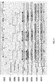
- FIG. 4 is an exemplary timing diagram of showing how the TCAM 3000 can perform simultaneous TCAM write and search operation, according to some embodiments.
- a TCAM 3000 may perform a simultaneous write operation and search operation by asserting both search enable 3009 (e.g. SR) and memory write enable 3007 (e.g. WE) signal in the same cycle.
- search enable 3009 and memory write enable 3007 are both asserted.
- FIG. 4 also shows internal write data bus to memory 4001 and internal search data bus 4002 which are further described in conjunction with FIG. 5 .
- memory write and memory search are performed simultaneously in each of the three cycles shown.
- both SR 3009 and WE 3007 are asserted.
- both SR 3009 and WE 3007 are asserted, commanding the memory to perform both a memory search and a memory write.
- the address to update is represented by '000' (expressed in hexadecimal) through the memory address 3002 and the data to write is represented by 'aaaaa' which is input through DI (Memory DATA) 3003.
- DI Memory DATA
- the data to search is represented by 'fffff which is input through SDI (Search DATA) 3004.
- the SR 3009 and WE 3007 are again both asserted, indicating that the memory should perform both search and write.
- the address to update is represented by '001' (expressed in hexadecimal) through the memory address 3002 and the data to write is represented by '55555' which is input through DI (Memory DATA) 3003.
- DI Memory DATA
- the memory is writing the mask stored in the Y address.
- the data to search is represented by '00000' which is input through SDI (Search DATA) 3004.
- the SR 3009 and WE 3007 are again both asserted.
- the address to update is represented by '002' (expressed in hexadecimals) through the memory address 3002 and the data to write is represented by 'aaaa' which is input through DI (Memory DATA) 3003.
- DI Memory DATA
- the memory is writing the data stored in the Y address.
- the data to search is represented by 'fffff which is input through SDI (Search DATA) 3004.
- FIG. 5 is an exemplary diagram of TCAM 3000 showing the TCAM interface, TCAM memory array 5009, and internal write and search data buses to the memory, according to some embodiments.
- the internal write bus may be used to write into the memory location represented by address bus A[m:0] 3002 and the internal search data bus may be used to search the contents of the TCAM memory array 5009 in the same cycle.
- the TCAM 3000 may include an input data buffer 3010 that receives data from the TCAM input interface 3050.
- Input data buffer 3010 may include a storage device 3010a, 3010b, etc., such as a latch or flip flop, for each row of the TCAM memory array 5009.
- the input data buffer 3010 may receive and be clocked by CLK 3001.
- the data inputs of the input data buffer are 3003 and 3004.
- the outputs of the input data buffer 3010 include an internal write data bus 4001 (e.g. data 4001a/dataB 4001b) to the memory and an internal search data bus 4002 (e.g. sdata 4002a/sdataB 4002b) to the memory.
- an internal write data bus 4001 e.g. data 4001a/dataB 4001b
- an internal search data bus 4002 e.g. sdata 4002a/sdataB 4002b
- the CAM device may include added circuity to disable the HIT output of the entry that is being updated in order to prevent the output of false hits.
- FIG. 6 is an exemplary diagram of a TCAM with circuitry configured to disable HIT outputs, according to some embodiments.
- a TCAM 3000 configured to perform write and search operations simultaneously may also comprise the circuitry, such as circuitry 6000, configured to disable HIT outputs of the entry that is being updated.
- the circuitry 6000 may receive the address 3002 of the entry being updated and ensure the corresponding HIT output of the TCAM memory array is not asserted. There are a number of ways in which this may be performed. An example of such circuitry 6000 is shown in FIG. 6 .
- circuitry 6000 includes a decoder that receives the address 3002 of the entry being updated and de-asserts the corresponding decoder output WL.
- the decoder outputs then proceed to a series of AND gates.
- the AND gates ensure that any output of the decoder that is asserted ensures corresponding HIT output of the output interface 3060 is not asserted. This prevents a false hit for the TCAM entry that is being updated.
- FIG. 7A-B and FIG. 8A-C illustrate embodiments of TCAM architectures and examples of timing diagrams wherein the TCAM is configured to perform write operations-including data writes and mask writes-in a single clock cycle.
- This architecture may be used in combination with the architecture described above for simultaneous write and search.
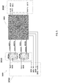
- FIG. 7A is a block diagram illustrating a TCAM architecture, in accordance with some embodiments.
- This architecture includes control circuitry 700 and TCAM 702.
- This architecture is designed to increase the speed of write operations into a TCAM relative to previous implementations. More specifically, this architecture is designed to write a data input and a mask in a single clock cycle. For example, in the same clock cycle, a data input may be written into data row 0 and a mask may be written into mask row 0.
- the buses of the TCAM are arranged to support write operations of data input and masks in single clock cycles.
- control circuitry 700 communicates with TCAM 702 using the following buses: CK, A, SDI, DI, MASKB, CS, WE, RD, SCU and SR.
- FIG. 7B illustrates a representative write operation sequence, in accordance with some embodiments.
- the figure illustrates the relationship between the signals of buses CLK, SCU, CS, WE, A, DI, SDI and MASKB.
- signal CS indicates that this TCAM chip has been selected.
- signal SCU indicates that a single clock operation is to be performed.
- signal WE indicates that regular write operation is not to be performed. Thus, assertion of these three signals indicates that a single clock cycle write operation is to be performed in this TCAM chip.
- Signal A provides the address of the row to be written.
- the address (expressed in hexadecimals) is "000.”
- the content of signal DI represents the data input to be written into the addressed TCAM data row.
- the content of DI is "aaaaa.”
- the content of signal SDI represents the mask to be written into the addressed TCAM mask row.
- the content of DI is "55555.” In this sequence, both the content of DI and the content of SDI are written in a single clock cycle.
- the content of signal MASKB (“ffffff' in this example) is not considered.
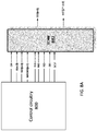
- FIG. 8A is a block diagram illustrating another TCAM architecture, in accordance with some embodiments. Similar to the architecture of FIG. 7A , this architecture is also designed to write a data input and a mask in a single clock cycle. However, this architecture involves fewer buses than the architecture of FIG. 7A , thereby reducing circuit complexity.
- This architecture includes control circuitry 800 and TCAM 802.
- the buses of the TCAM are arranged to support write operations of data input and masks in single clock cycles.
- control circuitry 800 communicates with TCAM 802 using the following buses: CK, A, SDI, MASKB, CS, WE, RD, SR, and SCU.
- bus DI bus DI
- both buses SDI and MASKB have a dual function.
- bus SDI carries the data input to be written and MASKB carries the mask to be written.
- bus SDI carries the key to be searched and MASKB carries mask bits identifying which column(s) are to be masked (although, alternatively, bus MASKB may carry the key to be searched and SDI may carry mask bits identifying which column(s) are to be masked).
- bus MASKB may carry the key to be searched and SDI may carry mask bits identifying which column(s) are to be masked.
- both SDI and MASKB are used in a time-multiplexed fashion.
- Buses CK, A, CS, WE, RD and SR have the same functions described in connection with FIG. 7A .
- Output bus DO and HIT also have the same functions described in connection with FIG. 7A .
- FIG. 8B illustrates an example of TCAM 802, in accordance with some embodiments.
- TCAM 802 includes flip-flops 850, 852 and 854, logic units 846, 848, 856 and 858, multiplexers 860 and 862, control unit 864 and TCAM array 870.
- TCAM array 870 may include SRAMs (or other types of memories).
- TCAM 802 receives signals through buses SDI, MASKB, CLK, WE, SCU and A (as discussed in connection with FIG. 8A ). In some embodiments, there may be a circuit similar to that of FIG. 8B for each column of the TCAM array.
- Logic unit 846 receives as input the signal of bus SDI and logic unit 848 receives as input the signal of bus MASKB.
- the signal of pin SCU indicates whether a write operation, including writing of a data input and a mask, is to be performed in a single clock cycle or not. In this example, SCU controls the state of logic unit 848.
- Flip-flop 850 receives as input the signal of bus SDI, flip-flop 852 receives as input the output of logic unit 846 and flip-flop 854 receives as input the output of logic unit 848. Clock CLK times the operations of the flip-flops. The outputs of flip-flop 850 are provided as inputs to multiplexers 860 and 862, respectively. The outputs of flip-flop 852 are provided as inputs to logic units 856 and 858, respectively. The state of the logic units 856 and 858 is controlled by the output of flip-flop 854.
- the signal of bus A indicates the address of the TCAM row to be written or read. During write operations, the signal of bus WE is asserted, which enables use of multiplexers 860 and 862 for write operations.
- control unit 364 enables writing into TCAM array 870, and the outputs of the flip-flops are written into the TCAM array, via transistors 866 and 868.
- the signal of bus A determines the address of the row to be written.
- logic units 856 and 858 mask the search of a particular row, depending on the value of the corresponding mask bit of MASKB.
- FIG. 8C illustrates a representative write operation sequence in connection with the architecture of FIG. 8A , in accordance with some embodiments.
- the figure illustrates the relationship between the signals of buses CLK, SCU, WE, A, SDI and MASKB. Assertion of SCU, CS and de-assertion of WE indicates that a single clock cycle write operation is to be performed in this TCAM chip.
- Signal A provides the address of the row to be written.
- the content of signal SDI represents the data input to be written into the addressed TCAM data row.
- the content of signal MASKB represents the mask to be written into the addressed TCAM mask row. In this sequence, both the content of SDI and the content of MASKB are written in a single clock cycle.
- a content addressable memory (CAM) device can include a CAM array that may have four data input buses.
- a primary DATA input e.g. DI[n:0]
- a secondary data input e.g. BYTE[n:0]
- MASK (Y) word of the CAM array represented by address bus e.g. A[m:1]
- a third data input e.g. SDI[n:0]
- a fourth data input e.g. MASKB[n:0]
- a simultaneous memory write operation of a CAM device may be performed in the array to update both DATA and MASK word in a single cycle, while searching its contents by asserting both the search enable (SR) and memory write enable (WE) signals in the same cycle.
- SR search enable
- WE memory write enable
- FIG. 9 is a block diagram illustrating another TCAM architecture, in accordance with some embodiments. Similar to the architecture of FIG. 7A and 8A , this architecture is also designed to write a data input and a mask in a single clock cycle. However, this architecture also includes 4 data input buses DI[n:0], BYTE[n:0], SDI[n:0], and MASKB[n:0] as described herein.
- This architecture includes control circuitry 900 and TCAM 902.
- the buses of the TCAM are arranged to support write operations of data input and masks in single clock cycles.
- control circuitry 900 communicates with TCAM 902 using the following buses: CK, A, SDI, DI, MASKB, CS, WE, RD, SR, SCU, and BYTE.
- a simultaneous memory write operation of the TCAM 902 may be performed in the array to update both DATA and MASK word in a single cycle, while searching its contents by asserting both the search enable (SR) and memory write enable (WE) signals in the same cycle.
- bus DI carries the data input to be written and BYTE carries the mask to be written.
- bus SDI carries the key to be searched and MASKB carries mask bits identifying which column(s) are to be masked (although, alternatively, bus MASKB may carry the key to be searched and SDI may carry mask bits identifying which column(s) are to be masked).
- Buses CK, A, CS, WE, RD and SR have the same functions described in connection with FIG. 7A and 8A .
- Output bus DO and HIT also have the same functions described in connection with FIG. 7A and 8A .
- Coupled or “connected” is meant to refer to circuit elements, or signals, that are either directly linked to one another or through intermediate components.
- the terms “approximately”, “substantially,” and “about” may be used to mean within ⁇ 20% of a target value in some embodiments, within ⁇ 10% of a target value in some embodiments, within ⁇ 5% of a target value in some embodiments, and within ⁇ 2% of a target value in some embodiments.
- the terms “approximately” and “about” may include the target value.
Landscapes
- Engineering & Computer Science (AREA)
- Multimedia (AREA)
- Static Random-Access Memory (AREA)
- Sanitary Device For Flush Toilet (AREA)
- Crystals, And After-Treatments Of Crystals (AREA)
- Radar Systems Or Details Thereof (AREA)
Abstract
Description
- Content-addressable memory (CAM) is a type of computer memory that is specifically designed for search-intensive applications. Some CAMs are designed to search their entire contents in a single clock cycle. Data stored in a CAM can be accessed by searching for the data itself, and the memory retrieves the addresses where that data is located. Because of its parallel nature, CAMs are much faster than random access memory (RAM) architectures for searching. CAMs are often used in internet routers and switches, where they increase the speed of route lookup, packet classification and packet forwarding.
- Some aspects relate to a ternary content addressable memory (TCAM) device. The TCAM device has an input interface having a first input for receiving first data and a second input for receiving second data and a memory configured to write the first data into an address selected row of the memory at the same time that a comparison is performed between the second data and at least one other row of the memory different from the address selected row.
- The first input may be a memory write bus.
- The second input may be a search data bus.
- The input interface may have a third input for receiving a search enable signal and a fourth input for receiving a write enable signal, wherein the memory is configured to write the first data and perform the comparison in response to assertion of the search enable signal at the same time as assertion of the write enable signal.
- The TCAM may further comprise an internal write data bus configured to receive the first data; and an internal search data bus configured to receive the second data.
- The TCAM may further comprise an input data buffer including a first storage device configured to receive the first data and provide the first data to the internal write data bus; and a second storage device configured to receive the second data and provide the second data to the internal search data bus.
- The first storage device may comprise a latch or a flip-flop.
- The TCAM device may further comprise circuitry configured to disable a HIT output corresponding to an entry of the memory being updated.
- The circuitry comprises a decoder that receives an address of the entry being updated and a plurality of AND gates.
- The TCAM device may be further configured to perform data and mask write operations in a single clock cycle.
- The at least one other row may comprise a plurality of rows.
- The plurality of rows may comprise all rows of the memory.
- Some aspects relate to a method of operating a ternary content addressable memory (TCAM) device. The method includes the steps of receiving, at an input interface, first data via a first input and second data via a second input; and writing the first data into an address selected row of a memory at the same time as performing a comparison between the second data and at least one other row of the memory different from the address selected row.
- The first input may be a memory write bus.
- The second input may be a search data bus.
- The method of operating the TCAM device may further comprise receiving a search enable signal and a write enable signal; and writing the first data and performing the comparison in response to assertion of the search enable signal at the same time as assertion of the write enable signal.
- The method may further comprise receiving the first data at an internal write data bus; and receiving the second data at an internal search data bus.
- The method may also comprise: by a first storage device, receiving the first data and providing the first data to the internal write data bus; and by a second storage device, receiving the second data and providing the second data to the internal search data bus.
- The first storage device may comprise a latch or a flip-flop.
- The method may further comprise disabling a HIT output corresponding to an entry of the memory being updated.
- The disabling may be performed by circuitry comprising a decoder that receives an address of the entry being updated and a plurality of AND gates.
- The method may further comprise performing data and mask write operations in a single clock cycle.
- The at least one other row may comprise a plurality of rows.
- The plurality of rows may be all rows of the memory.
- The foregoing summary is provided by way of illustration and is not intended to be limiting.
- The accompanying drawings are not intended to be drawn to scale. In the drawings, each identical or nearly identical component that is illustrated in various figures is represented by a like numeral. For purposes of clarity, not every component may be labeled in every drawing.
-
FIG. 1A is an exemplary diagram of a representative ternary content addressable memory, according to conventional systems. -
FIG. 1B is an exemplary diagram of a TCAM entry, according to some embodiments. -
FIG. 2 is an exemplary diagram of a timing diagram for TCAM write and search operation in different cycles, according to conventional systems. -
FIG. 3 is an exemplary diagram of a TCAM input/output interface, according to some embodiments. -
FIG. 4 is an exemplary diagram of a timing diagram for simultaneous TCAM write and search operation, according to some embodiments. -
FIG. 5 is an exemplary diagram of a content addressable memory comprising internal write and search data buses to the memory, according to some embodiments. -
FIG. 6 is an exemplary diagram of a TCAM with circuitry configured to disable HIT outputs, according to some embodiments. -
FIG. 7A is a block diagram illustrating a TCAM architecture, in accordance with some embodiments. -
FIG. 7B is a diagram illustrating control signals, according to some embodiments. -
FIG. 8A is a block diagram illustrating another TCAM architecture, according to some embodiments. -
FIG. 8B is a block diagram illustrating an example of an implementation of the TCAM architecture ofFIG. 8A , according to some embodiments. -
FIG. 8C is a diagram illustrating control signals used in connection with the TCAM architecture ofFIG. 8A , according to some embodiments. -
FIG. 9 is a block diagram illustrating another TCAM architecture, in accordance with some embodiments. - Content-addressable memory (CAM) such as Ternary Content Addressable Memory (TCAM) can be used in high performance enterprise and data center switching ASICs (both embedded and standalone) to perform packet classification and forwarding. TCAM can enable high throughput classification by performing fast and parallel look ups by matching incoming packet headers with predefined rules stored in Access Control Lists (ACLs) look up tables. ACL look up table rules may be updated periodically to adapt to changing network traffic patterns. In some cases, to preserve priority of rules, a rule update in memory will result in shuffling many entries. In conventional systems, the lookup operation is paused while the rules are updating in the memory, resulting in a performance limitation.
- The inventors have recognized and appreciated that the performance of such systems and operations may be improved by designing a TCAM that can perform entry updates in the background while continuing to search other entries. The inventors have developed techniques and circuitry that can perform both the look up operation and the rule update operation simultaneously, for example, in a single clock cycle.
-
FIG. 1A is an exemplary diagram of a ternary content addressable memory (TCAM) 1000. A TCAM may have '2m+1' (m>0) number of rows, and 'n+1' columns, each of the rows comprising 'n+1' TCAM cells.TCAM 1000 receives inputs includingclock signal CK 1001, input memory address bus A[m:0] 1002, input search bus SDI[n:0] 1003, chip select (CS) 1004, write enable (WE) 1005, read (RD) 1006, search (SR) 1007 and mask data bus MASKB[n:0] 1008. - Input memory address bus A[m:0] 1002 may indicate which of the 2m TCAM entries to write into memory. Input search bus SDI[n:0] 1003 may represent the data used to search the memory array during a search operation.
WE 1005 is an input to enable a memory write operation.RD 1006 is an input to enable a memory read operation.SR 1007 is an input to enable a search operation. -
FIG. 1B is an exemplary diagram of TCAM entries, according to some embodiments. TCAM entries may be organized by masks. Accordingly, in some embodiments, in order to update a TCAM entry, both the data and mask of the entry may be updated. InFIG. 1B ,SRAM X word 1202, representing data, andSRAM Y word 1203, representing the mask, may both need to be updated. -
FIG. 2 is an exemplary timing diagram of a TCAM that performs write and search operations in different cycles, for the TCAM ofFIG. 1A .FIG. 2 shows memory write operations are performed during the first two clock cycles, and a search operation is performed during a separate clock cycle after the write operations. At no point are both theSR 1007 and WE 1005 both asserted (high logic level, for example) at the same time. In the first memory write cycle, the write enable WE signal 1005 is asserted. This indicates that the TCAM should perform a write operation. In this first memory write cycle, the address to update is represented by '000' (expressed in hexadecimal) through the memory address and the data to write is represented by 'aaaaa' which is input through SDI (DATA) 1003. In this example, the memory is writing the data stored in the X address. In the second memory write cycle, the write enable WE signal 1005 is asserted, indicating that the TCAM should perform a write operation. In this second memory write cycle, the address to update is represented by '001' (expressed in hexadecimal) through the inputmemory address bus 1002, and the data to write is represented by '55555' which is input through SDI (DATA) 1003. In the second memory write cycle, the memory is writing the mask stored in the Y address. In the next (third) memory clock cycle, the write enable WE signal 1005 is not asserted. Instead, theSR 1007 is asserted, indicating that the TCAM should perform a search operation. In this cycle, the memory address is not used, and the data to search is represented by 'fffff which is input through SDI (DATA) 1003. -
FIG. 3 is an exemplary diagram of a TCAM input/output interface for aTCAM 3000 that enables searching at the same time as a write operation is performed, according to some embodiments. The TCAM input/output interface includes aTCAM input interface 3050 and aTCAM output interface 3060. More specifically, this architecture is designed to both write and search data in a single clock cycle. TheTCAM 3000 may have '2m+1' (m>0) number of rows, and 'n+1' columns, each of the rows comprising 'n+1' TCAM cells coupled to a match line.TCAM 3000 receives inputs includingclock signal CK 3001, input memory address bus A[m:0] 3002, memory write bus DI[n:0] 3003, input search bus SDI[n:0] 3004, mask data bus MASKB[n:0] 3005,CS 3006, WE 3007,RD 3008 andSR 3009. TheTCAM 3000 includes thememory write bus 3003 in addition to theinput search bus 3004, whereas theTCAM 1000 does not include thememory write bus 3003. In some embodiments, having separatememory write bus 3003 andsearch bus SDI 3004 allows for the simultaneous transfer of write data and search data, as opposed to having one SDI, such asSDI 1003 inFIG. 2 , which allows only write data or search data to be signaled at a time. -
FIG. 4 is an exemplary timing diagram of showing how theTCAM 3000 can perform simultaneous TCAM write and search operation, according to some embodiments. In some embodiments, aTCAM 3000 may perform a simultaneous write operation and search operation by asserting both search enable 3009 (e.g. SR) and memory write enable 3007 (e.g. WE) signal in the same cycle. In this exemplary diagram, search enable 3009 and memory write enable 3007 are both asserted.FIG. 4 also shows internal write data bus tomemory 4001 and internalsearch data bus 4002 which are further described in conjunction withFIG. 5 . - As shown in
FIG. 4 , memory write and memory search are performed simultaneously in each of the three cycles shown. In all three cycles, bothSR 3009 and WE 3007 are asserted. For example, in the first cycle, bothSR 3009 and WE 3007 are asserted, commanding the memory to perform both a memory search and a memory write. In the first cycle, the address to update is represented by '000' (expressed in hexadecimal) through thememory address 3002 and the data to write is represented by 'aaaaa' which is input through DI (Memory DATA) 3003. In the first cycle, the memory is writing the data stored in the X address. Simultaneously, the data to search is represented by 'fffff which is input through SDI (Search DATA) 3004. In the second cycle, theSR 3009 and WE 3007 are again both asserted, indicating that the memory should perform both search and write. The address to update is represented by '001' (expressed in hexadecimal) through thememory address 3002 and the data to write is represented by '55555' which is input through DI (Memory DATA) 3003. In this cycle, the memory is writing the mask stored in the Y address. Simultaneously, the data to search is represented by '00000' which is input through SDI (Search DATA) 3004. In the third cycle, theSR 3009 and WE 3007 are again both asserted. The address to update is represented by '002' (expressed in hexadecimals) through thememory address 3002 and the data to write is represented by 'aaaaa' which is input through DI (Memory DATA) 3003. In this example, the memory is writing the data stored in the Y address. Simultaneously, the data to search is represented by 'fffff which is input through SDI (Search DATA) 3004. -
FIG. 5 is an exemplary diagram ofTCAM 3000 showing the TCAM interface,TCAM memory array 5009, and internal write and search data buses to the memory, according to some embodiments. The internal write bus may be used to write into the memory location represented by address bus A[m:0] 3002 and the internal search data bus may be used to search the contents of theTCAM memory array 5009 in the same cycle. TheTCAM 3000 may include aninput data buffer 3010 that receives data from theTCAM input interface 3050.Input data buffer 3010 may include astorage device 3010a, 3010b, etc., such as a latch or flip flop, for each row of theTCAM memory array 5009. Theinput data buffer 3010 may receive and be clocked byCLK 3001. In this example the data inputs of the input data buffer are 3003 and 3004. The outputs of theinput data buffer 3010 include an internal write data bus 4001 (e.g. data 4001a/dataB 4001b) to the memory and an internal search data bus 4002 (e.g. sdata 4002a/sdataB 4002b) to the memory. - Simultaneous write and search operations may lead to false hits in the case of an entry that is being updated during a given clock cycle. In some embodiments, the CAM device may include added circuity to disable the HIT output of the entry that is being updated in order to prevent the output of false hits.
-
FIG. 6 is an exemplary diagram of a TCAM with circuitry configured to disable HIT outputs, according to some embodiments. In some embodiments, aTCAM 3000, configured to perform write and search operations simultaneously may also comprise the circuitry, such ascircuitry 6000, configured to disable HIT outputs of the entry that is being updated. Thecircuitry 6000 may receive theaddress 3002 of the entry being updated and ensure the corresponding HIT output of the TCAM memory array is not asserted. There are a number of ways in which this may be performed. An example ofsuch circuitry 6000 is shown inFIG. 6 . In this example,circuitry 6000 includes a decoder that receives theaddress 3002 of the entry being updated and de-asserts the corresponding decoder output WL. After being stored in a latch or flip flop the decoder outputs then proceed to a series of AND gates. The AND gates ensure that any output of the decoder that is asserted ensures corresponding HIT output of theoutput interface 3060 is not asserted. This prevents a false hit for the TCAM entry that is being updated. -
FIG. 7A-B andFIG. 8A-C illustrate embodiments of TCAM architectures and examples of timing diagrams wherein the TCAM is configured to perform write operations-including data writes and mask writes-in a single clock cycle. This architecture may be used in combination with the architecture described above for simultaneous write and search. -
FIG. 7A is a block diagram illustrating a TCAM architecture, in accordance with some embodiments. This architecture includescontrol circuitry 700 andTCAM 702. This architecture is designed to increase the speed of write operations into a TCAM relative to previous implementations. More specifically, this architecture is designed to write a data input and a mask in a single clock cycle. For example, in the same clock cycle, a data input may be written intodata row 0 and a mask may be written intomask row 0. The buses of the TCAM are arranged to support write operations of data input and masks in single clock cycles. As shown inFIG. 7A ,control circuitry 700 communicates withTCAM 702 using the following buses: CK, A, SDI, DI, MASKB, CS, WE, RD, SCU and SR. -
FIG. 7B illustrates a representative write operation sequence, in accordance with some embodiments. The figure illustrates the relationship between the signals of buses CLK, SCU, CS, WE, A, DI, SDI and MASKB. When asserted (1-level in this example), signal CS indicates that this TCAM chip has been selected. When asserted (1-level in this example), signal SCU indicates that a single clock operation is to be performed. When de-asserted (0-level in this example), signal WE indicates that regular write operation is not to be performed. Thus, assertion of these three signals indicates that a single clock cycle write operation is to be performed in this TCAM chip. - Signal A provides the address of the row to be written. In this example, the address (expressed in hexadecimals) is "000." The content of signal DI represents the data input to be written into the addressed TCAM data row. In this example, the content of DI is "aaaaa." The content of signal SDI represents the mask to be written into the addressed TCAM mask row. In this example, the content of DI is "55555." In this sequence, both the content of DI and the content of SDI are written in a single clock cycle. During the write operation, the content of signal MASKB ("fffff' in this example) is not considered.
-
FIG. 8A is a block diagram illustrating another TCAM architecture, in accordance with some embodiments. Similar to the architecture ofFIG. 7A , this architecture is also designed to write a data input and a mask in a single clock cycle. However, this architecture involves fewer buses than the architecture ofFIG. 7A , thereby reducing circuit complexity. - This architecture includes
control circuitry 800 andTCAM 802. The buses of the TCAM are arranged to support write operations of data input and masks in single clock cycles. As shown inFIG. 8A ,control circuitry 800 communicates withTCAM 802 using the following buses: CK, A, SDI, MASKB, CS, WE, RD, SR, and SCU. It should be noted that, unlike the example ofFIG. 7A , this architecture does not include bus DI. In this architecture, both buses SDI and MASKB have a dual function. During a write operation, bus SDI carries the data input to be written and MASKB carries the mask to be written. During a search operation, bus SDI carries the key to be searched and MASKB carries mask bits identifying which column(s) are to be masked (although, alternatively, bus MASKB may carry the key to be searched and SDI may carry mask bits identifying which column(s) are to be masked). In essence, both SDI and MASKB are used in a time-multiplexed fashion. Buses CK, A, CS, WE, RD and SR have the same functions described in connection withFIG. 7A . Output bus DO and HIT also have the same functions described in connection withFIG. 7A . -
FIG. 8B illustrates an example ofTCAM 802, in accordance with some embodiments. In this implementation,TCAM 802 includes flip-flops logic units multiplexers control unit 864 andTCAM array 870.TCAM array 870 may include SRAMs (or other types of memories).TCAM 802 receives signals through buses SDI, MASKB, CLK, WE, SCU and A (as discussed in connection withFIG. 8A ). In some embodiments, there may be a circuit similar to that ofFIG. 8B for each column of the TCAM array. -
Logic unit 846 receives as input the signal of bus SDI andlogic unit 848 receives as input the signal of bus MASKB. The signal of pin SCU indicates whether a write operation, including writing of a data input and a mask, is to be performed in a single clock cycle or not. In this example, SCU controls the state oflogic unit 848. - Flip-
flop 850 receives as input the signal of bus SDI, flip-flop 852 receives as input the output oflogic unit 846 and flip-flop 854 receives as input the output oflogic unit 848. Clock CLK times the operations of the flip-flops. The outputs of flip-flop 850 are provided as inputs tomultiplexers flop 852 are provided as inputs tologic units logic units flop 854. The signal of bus A indicates the address of the TCAM row to be written or read. During write operations, the signal of bus WE is asserted, which enables use ofmultiplexers TCAM array 870, and the outputs of the flip-flops are written into the TCAM array, viatransistors logic units -
FIG. 8C illustrates a representative write operation sequence in connection with the architecture ofFIG. 8A , in accordance with some embodiments. The figure illustrates the relationship between the signals of buses CLK, SCU, WE, A, SDI and MASKB. Assertion of SCU, CS and de-assertion of WE indicates that a single clock cycle write operation is to be performed in this TCAM chip. - Signal A provides the address of the row to be written. The content of signal SDI represents the data input to be written into the addressed TCAM data row. The content of signal MASKB represents the mask to be written into the addressed TCAM mask row. In this sequence, both the content of SDI and the content of MASKB are written in a single clock cycle.
- According to some embodiments, a content addressable memory (CAM) device can include a CAM array that may have four data input buses. In some embodiments, a primary DATA input (e.g. DI[n:0]) can be used to write into the DATA (X) word of the CAM memory and a secondary data input (e.g. BYTE[n:0]) may be used to write into MASK (Y) word of the CAM array represented by address bus (e.g. A[m:1]) in a single cycle. In some embodiments, a third data input (e.g. SDI[n:0]) and a fourth data input (e.g. MASKB[n:0]) may be used to supply the search key and mask key for the search function respectively. According to some embodiments, a simultaneous memory write operation of a CAM device may be performed in the array to update both DATA and MASK word in a single cycle, while searching its contents by asserting both the search enable (SR) and memory write enable (WE) signals in the same cycle.
-
FIG. 9 is a block diagram illustrating another TCAM architecture, in accordance with some embodiments. Similar to the architecture ofFIG. 7A and8A , this architecture is also designed to write a data input and a mask in a single clock cycle. However, this architecture also includes 4 data input buses DI[n:0], BYTE[n:0], SDI[n:0], and MASKB[n:0] as described herein. - This architecture includes
control circuitry 900 andTCAM 902. The buses of the TCAM are arranged to support write operations of data input and masks in single clock cycles. As shown inFIG. 9A ,control circuitry 900 communicates withTCAM 902 using the following buses: CK, A, SDI, DI, MASKB, CS, WE, RD, SR, SCU, and BYTE. A simultaneous memory write operation of theTCAM 902 may be performed in the array to update both DATA and MASK word in a single cycle, while searching its contents by asserting both the search enable (SR) and memory write enable (WE) signals in the same cycle. - During a write operation, bus DI carries the data input to be written and BYTE carries the mask to be written. During a search operation, bus SDI carries the key to be searched and MASKB carries mask bits identifying which column(s) are to be masked (although, alternatively, bus MASKB may carry the key to be searched and SDI may carry mask bits identifying which column(s) are to be masked). Buses CK, A, CS, WE, RD and SR have the same functions described in connection with
FIG. 7A and8A . Output bus DO and HIT also have the same functions described in connection withFIG. 7A and8A . - Use of ordinal terms such as "first", "second", "third", etc., in the claims to modify a claim element does not by itself connote any priority, precedence, or order of one claim element over another or the temporal order in which acts of a method are performed, but are used merely as labels to distinguish one claim element having a certain name from another element having a same name (but for use of the ordinal term) to distinguish the claim elements.
- Also, the phraseology and terminology used herein is for the purpose of description and should not be regarded as limiting. The use of "including", "comprising", "having", "containing" or "involving" and variations thereof herein, is meant to encompass the items listed thereafter and equivalents thereof as well as additional items.
- The use of "coupled" or "connected" is meant to refer to circuit elements, or signals, that are either directly linked to one another or through intermediate components.
- The terms "approximately", "substantially," and "about" may be used to mean within ±20% of a target value in some embodiments, within ±10% of a target value in some embodiments, within ±5% of a target value in some embodiments, and within ±2% of a target value in some embodiments. The terms "approximately" and "about" may include the target value.
Claims (15)
- A ternary content addressable memory (TCAM) device comprising:an input interface having a first input for receiving first data and a second input for receiving second data; anda memory configured to write the first data into an address selected row of the memory at the same time that a comparison is performed between the second data and at least one other row of the memory different from the address selected row.
- The TCAM device of claim 1, wherein the first input is a memory write bus.
- The TCAM device of any preceding claim, wherein the second input is a search data bus.
- The TCAM device of any preceding claim, wherein the input interface has a third input for receiving a search enable signal and a fourth input for receiving a write enable signal, wherein the memory is configured to write the first data and perform the comparison in response to assertion of the search enable signal at the same time as assertion of the write enable signal.
- The TCAM device of any preceding claim, further comprising:an internal write data bus configured to receive the first data; andan internal search data bus configured to receive the second data.
- The TCAM device of claim 5, further comprising an input data buffer including:a first storage device configured to receive the first data and provide the first data to the internal write data bus; anda second storage device configured to receive the second data and provide the second data to the internal search data bus.
- The TCAM device of any preceding claim, further comprising circuitry configured to disable a HIT output corresponding to an entry of the memory being updated.
- The TCAM device of any preceding claim, wherein the TCAM device is further configured to perform data and mask write operations in a single clock cycle.
- A method of operating a ternary content addressable memory (TCAM) device, the method comprising:receiving, at an input interface, first data via a first input and second data via a second input; andwrite the first data into an address selected row of a memory at the same time as performing a comparison between the second data and at least one other row of the memory different from the address selected row.
- The method of claim 9, wherein the first input is a memory write bus.
- The method of claim 9 or claim 10, wherein the second input is a search data bus.
- The method of any one of claims 9-11, further comprising:receiving a search enable signal and a write enable signal; andwriting the first data and performing the comparison in response to assertion of the search enable signal at the same time as assertion of the write enable signal.
- The method of any one of claims 9-12, further comprising:receiving the first data at an internal write data bus; andreceiving the second data at an internal search data bus.
- The method of claim 13, further comprising:by a first storage device, receiving the first data and providing the first data to the internal write data bus; andby a second storage device, receiving the second data and providing the second data to the internal search data bus.
- The method of any one of claims 9-14, further comprising performing data and mask write operations in a single clock cycle.
Applications Claiming Priority (2)
| Application Number | Priority Date | Filing Date | Title |
|---|---|---|---|
| IN202021012615 | 2020-03-23 | ||
| US17/193,853 US11557328B2 (en) | 2020-03-23 | 2021-03-05 | Simultaneous write and search operation in a content addressable memory |
Publications (2)
| Publication Number | Publication Date |
|---|---|
| EP3886098A1 true EP3886098A1 (en) | 2021-09-29 |
| EP3886098B1 EP3886098B1 (en) | 2024-08-28 |
Family
ID=74884898
Family Applications (1)
| Application Number | Title | Priority Date | Filing Date |
|---|---|---|---|
| EP21162879.7A Active EP3886098B1 (en) | 2020-03-23 | 2021-03-16 | Simultaneous write and search operation in a content addressable memory |
Country Status (2)
| Country | Link |
|---|---|
| EP (1) | EP3886098B1 (en) |
| TW (1) | TWI777456B (en) |
Citations (1)
| Publication number | Priority date | Publication date | Assignee | Title |
|---|---|---|---|---|
| EP1083572A1 (en) * | 1999-09-10 | 2001-03-14 | Sibercore Technologies, Inc. | Three port content addressable memory device and methods for implementing the same |
Family Cites Families (5)
| Publication number | Priority date | Publication date | Assignee | Title |
|---|---|---|---|---|
| US6839256B1 (en) * | 2002-03-15 | 2005-01-04 | Integrated Device Technology, Inc. | Content addressable memory (CAM) devices having dedicated mask cell sub-arrays therein and methods of operating same |
| JP4541077B2 (en) * | 2004-01-13 | 2010-09-08 | 株式会社日立超エル・エス・アイ・システムズ | Semiconductor memory device |
| US8228703B2 (en) * | 2008-11-04 | 2012-07-24 | Crocus Technology Sa | Ternary Content Addressable Magnetoresistive random access memory cell |
| US7907432B2 (en) * | 2009-06-30 | 2011-03-15 | Netlogic Microsystems, Inc. | Content addressable memory device for simultaneously searching multiple flows |
| JP7091918B2 (en) * | 2018-08-02 | 2022-06-28 | 株式会社ソシオネクスト | Semiconductor storage device and its control method |
-
2021
- 2021-03-16 EP EP21162879.7A patent/EP3886098B1/en active Active
- 2021-03-18 TW TW110109730A patent/TWI777456B/en active
Patent Citations (1)
| Publication number | Priority date | Publication date | Assignee | Title |
|---|---|---|---|---|
| EP1083572A1 (en) * | 1999-09-10 | 2001-03-14 | Sibercore Technologies, Inc. | Three port content addressable memory device and methods for implementing the same |
Also Published As
| Publication number | Publication date |
|---|---|
| EP3886098B1 (en) | 2024-08-28 |
| TWI777456B (en) | 2022-09-11 |
| TW202137214A (en) | 2021-10-01 |
Similar Documents
| Publication | Publication Date | Title |
|---|---|---|
| US6502163B1 (en) | Method and apparatus for ordering entries in a ternary content addressable memory | |
| US6876559B1 (en) | Block-writable content addressable memory device | |
| US6751110B2 (en) | Static content addressable memory cell | |
| US7382637B1 (en) | Block-writable content addressable memory device | |
| US7193874B1 (en) | Content addressable memory device | |
| US6731526B2 (en) | CAM cell array, TCAM cell, TCAM cell array, address search memory, and network address search apparatus | |
| US11557328B2 (en) | Simultaneous write and search operation in a content addressable memory | |
| US7602629B2 (en) | Content addressable memory | |
| US6744654B2 (en) | High density dynamic ternary-CAM memory architecture | |
| US9025354B2 (en) | Power limiting in a content search system | |
| JP2017037700A (en) | Pseudo-nor cell for ternary content addressable memory | |
| US7219188B1 (en) | Segmented content addressable memory array and priority encoder | |
| US7113415B1 (en) | Match line pre-charging in a content addressable memory having configurable rows | |
| US7251707B1 (en) | Content based content addressable memory block enabling using search key | |
| US11886746B1 (en) | Algorithmic TCAM with storage activity-based read | |
| US7228378B1 (en) | Entry location in a content addressable memory | |
| US20040128440A1 (en) | Distributed programmable priority encoder capable of finding the longest match in a single operation | |
| US7920399B1 (en) | Low power content addressable memory device having selectable cascaded array segments | |
| EP3886098B1 (en) | Simultaneous write and search operation in a content addressable memory | |
| US11894054B2 (en) | Methods for writing ternary content addressable memory devices | |
| US11404121B2 (en) | Methods for writing ternary content addressable memory devices | |
| CN114758704B (en) | Content-Addressable Memory and its Operation Methods | |
| TWI802980B (en) | An apparatus for writing ternary content addressable memory devices and the related method | |
| EP3813068A1 (en) | Methods for writing ternary content addressable memory devices | |
| JP5631278B2 (en) | Content reference memory |
Legal Events
| Date | Code | Title | Description |
|---|---|---|---|
| PUAI | Public reference made under article 153(3) epc to a published international application that has entered the european phase |
Free format text: ORIGINAL CODE: 0009012 |
|
| STAA | Information on the status of an ep patent application or granted ep patent |
Free format text: STATUS: THE APPLICATION HAS BEEN PUBLISHED |
|
| AK | Designated contracting states |
Kind code of ref document: A1 Designated state(s): AL AT BE BG CH CY CZ DE DK EE ES FI FR GB GR HR HU IE IS IT LI LT LU LV MC MK MT NL NO PL PT RO RS SE SI SK SM TR |
|
| STAA | Information on the status of an ep patent application or granted ep patent |
Free format text: STATUS: REQUEST FOR EXAMINATION WAS MADE |
|
| 17P | Request for examination filed |
Effective date: 20220328 |
|
| RBV | Designated contracting states (corrected) |
Designated state(s): AL AT BE BG CH CY CZ DE DK EE ES FI FR GB GR HR HU IE IS IT LI LT LU LV MC MK MT NL NO PL PT RO RS SE SI SK SM TR |
|
| P01 | Opt-out of the competence of the unified patent court (upc) registered |
Effective date: 20230627 |
|
| STAA | Information on the status of an ep patent application or granted ep patent |
Free format text: STATUS: EXAMINATION IS IN PROGRESS |
|
| 17Q | First examination report despatched |
Effective date: 20230926 |
|
| REG | Reference to a national code |
Ref country code: DE Ref legal event code: R079 Free format text: PREVIOUS MAIN CLASS: G11C0007100000 Ipc: G11C0015040000 Ref country code: DE Ref legal event code: R079 Ref document number: 602021017740 Country of ref document: DE Free format text: PREVIOUS MAIN CLASS: G11C0007100000 Ipc: G11C0015040000 |
|
| GRAP | Despatch of communication of intention to grant a patent |
Free format text: ORIGINAL CODE: EPIDOSNIGR1 |
|
| STAA | Information on the status of an ep patent application or granted ep patent |
Free format text: STATUS: GRANT OF PATENT IS INTENDED |
|
| RIC1 | Information provided on ipc code assigned before grant |
Ipc: G11C 7/10 20060101ALI20240301BHEP Ipc: G11C 15/00 20060101ALI20240301BHEP Ipc: G11C 15/04 20060101AFI20240301BHEP |
|
| RIN1 | Information on inventor provided before grant (corrected) |
Inventor name: NARVEKAR, GAURANG PRABHAKAR Inventor name: GARG, RITESH Inventor name: JEDHE, GAJANAN SAHEBRAO Inventor name: DESHPANDE, CHETAN |
|
| INTG | Intention to grant announced |
Effective date: 20240325 |
|
| RAP3 | Party data changed (applicant data changed or rights of an application transferred) |
Owner name: MEDIATEK SINGAPORE PTE. LTD. |
|
| GRAS | Grant fee paid |
Free format text: ORIGINAL CODE: EPIDOSNIGR3 |
|
| GRAA | (expected) grant |
Free format text: ORIGINAL CODE: 0009210 |
|
| STAA | Information on the status of an ep patent application or granted ep patent |
Free format text: STATUS: THE PATENT HAS BEEN GRANTED |
|
| AK | Designated contracting states |
Kind code of ref document: B1 Designated state(s): AL AT BE BG CH CY CZ DE DK EE ES FI FR GB GR HR HU IE IS IT LI LT LU LV MC MK MT NL NO PL PT RO RS SE SI SK SM TR |
|
| REG | Reference to a national code |
Ref country code: CH Ref legal event code: EP |
|
| REG | Reference to a national code |
Ref country code: DE Ref legal event code: R096 Ref document number: 602021017740 Country of ref document: DE |
|
| REG | Reference to a national code |
Ref country code: IE Ref legal event code: FG4D |
|
| REG | Reference to a national code |
Ref country code: LT Ref legal event code: MG9D |
|
| PG25 | Lapsed in a contracting state [announced via postgrant information from national office to epo] |
Ref country code: NO Free format text: LAPSE BECAUSE OF FAILURE TO SUBMIT A TRANSLATION OF THE DESCRIPTION OR TO PAY THE FEE WITHIN THE PRESCRIBED TIME-LIMIT Effective date: 20241128 |
|
| REG | Reference to a national code |
Ref country code: AT Ref legal event code: MK05 Ref document number: 1718905 Country of ref document: AT Kind code of ref document: T Effective date: 20240828 |
|
| PG25 | Lapsed in a contracting state [announced via postgrant information from national office to epo] |
Ref country code: NL Free format text: LAPSE BECAUSE OF FAILURE TO SUBMIT A TRANSLATION OF THE DESCRIPTION OR TO PAY THE FEE WITHIN THE PRESCRIBED TIME-LIMIT Effective date: 20240828 Ref country code: PT Free format text: LAPSE BECAUSE OF FAILURE TO SUBMIT A TRANSLATION OF THE DESCRIPTION OR TO PAY THE FEE WITHIN THE PRESCRIBED TIME-LIMIT Effective date: 20241230 Ref country code: GR Free format text: LAPSE BECAUSE OF FAILURE TO SUBMIT A TRANSLATION OF THE DESCRIPTION OR TO PAY THE FEE WITHIN THE PRESCRIBED TIME-LIMIT Effective date: 20241129 Ref country code: PL Free format text: LAPSE BECAUSE OF FAILURE TO SUBMIT A TRANSLATION OF THE DESCRIPTION OR TO PAY THE FEE WITHIN THE PRESCRIBED TIME-LIMIT Effective date: 20240828 Ref country code: FI Free format text: LAPSE BECAUSE OF FAILURE TO SUBMIT A TRANSLATION OF THE DESCRIPTION OR TO PAY THE FEE WITHIN THE PRESCRIBED TIME-LIMIT Effective date: 20240828 |
|
| PG25 | Lapsed in a contracting state [announced via postgrant information from national office to epo] |
Ref country code: BG Free format text: LAPSE BECAUSE OF FAILURE TO SUBMIT A TRANSLATION OF THE DESCRIPTION OR TO PAY THE FEE WITHIN THE PRESCRIBED TIME-LIMIT Effective date: 20240828 |
|
| PG25 | Lapsed in a contracting state [announced via postgrant information from national office to epo] |
Ref country code: LV Free format text: LAPSE BECAUSE OF FAILURE TO SUBMIT A TRANSLATION OF THE DESCRIPTION OR TO PAY THE FEE WITHIN THE PRESCRIBED TIME-LIMIT Effective date: 20240828 |
|
| REG | Reference to a national code |
Ref country code: NL Ref legal event code: MP Effective date: 20240828 |
|
| PG25 | Lapsed in a contracting state [announced via postgrant information from national office to epo] |
Ref country code: AT Free format text: LAPSE BECAUSE OF FAILURE TO SUBMIT A TRANSLATION OF THE DESCRIPTION OR TO PAY THE FEE WITHIN THE PRESCRIBED TIME-LIMIT Effective date: 20240828 Ref country code: IS Free format text: LAPSE BECAUSE OF FAILURE TO SUBMIT A TRANSLATION OF THE DESCRIPTION OR TO PAY THE FEE WITHIN THE PRESCRIBED TIME-LIMIT Effective date: 20241228 |
|
| PG25 | Lapsed in a contracting state [announced via postgrant information from national office to epo] |
Ref country code: HR Free format text: LAPSE BECAUSE OF FAILURE TO SUBMIT A TRANSLATION OF THE DESCRIPTION OR TO PAY THE FEE WITHIN THE PRESCRIBED TIME-LIMIT Effective date: 20240828 |
|
| PG25 | Lapsed in a contracting state [announced via postgrant information from national office to epo] |
Ref country code: ES Free format text: LAPSE BECAUSE OF FAILURE TO SUBMIT A TRANSLATION OF THE DESCRIPTION OR TO PAY THE FEE WITHIN THE PRESCRIBED TIME-LIMIT Effective date: 20240828 Ref country code: RS Free format text: LAPSE BECAUSE OF FAILURE TO SUBMIT A TRANSLATION OF THE DESCRIPTION OR TO PAY THE FEE WITHIN THE PRESCRIBED TIME-LIMIT Effective date: 20241128 |
|
| PG25 | Lapsed in a contracting state [announced via postgrant information from national office to epo] |
Ref country code: RS Free format text: LAPSE BECAUSE OF FAILURE TO SUBMIT A TRANSLATION OF THE DESCRIPTION OR TO PAY THE FEE WITHIN THE PRESCRIBED TIME-LIMIT Effective date: 20241128 Ref country code: PT Free format text: LAPSE BECAUSE OF FAILURE TO SUBMIT A TRANSLATION OF THE DESCRIPTION OR TO PAY THE FEE WITHIN THE PRESCRIBED TIME-LIMIT Effective date: 20241230 Ref country code: PL Free format text: LAPSE BECAUSE OF FAILURE TO SUBMIT A TRANSLATION OF THE DESCRIPTION OR TO PAY THE FEE WITHIN THE PRESCRIBED TIME-LIMIT Effective date: 20240828 Ref country code: NO Free format text: LAPSE BECAUSE OF FAILURE TO SUBMIT A TRANSLATION OF THE DESCRIPTION OR TO PAY THE FEE WITHIN THE PRESCRIBED TIME-LIMIT Effective date: 20241128 Ref country code: NL Free format text: LAPSE BECAUSE OF FAILURE TO SUBMIT A TRANSLATION OF THE DESCRIPTION OR TO PAY THE FEE WITHIN THE PRESCRIBED TIME-LIMIT Effective date: 20240828 Ref country code: LV Free format text: LAPSE BECAUSE OF FAILURE TO SUBMIT A TRANSLATION OF THE DESCRIPTION OR TO PAY THE FEE WITHIN THE PRESCRIBED TIME-LIMIT Effective date: 20240828 Ref country code: IS Free format text: LAPSE BECAUSE OF FAILURE TO SUBMIT A TRANSLATION OF THE DESCRIPTION OR TO PAY THE FEE WITHIN THE PRESCRIBED TIME-LIMIT Effective date: 20241228 Ref country code: HR Free format text: LAPSE BECAUSE OF FAILURE TO SUBMIT A TRANSLATION OF THE DESCRIPTION OR TO PAY THE FEE WITHIN THE PRESCRIBED TIME-LIMIT Effective date: 20240828 Ref country code: GR Free format text: LAPSE BECAUSE OF FAILURE TO SUBMIT A TRANSLATION OF THE DESCRIPTION OR TO PAY THE FEE WITHIN THE PRESCRIBED TIME-LIMIT Effective date: 20241129 Ref country code: FI Free format text: LAPSE BECAUSE OF FAILURE TO SUBMIT A TRANSLATION OF THE DESCRIPTION OR TO PAY THE FEE WITHIN THE PRESCRIBED TIME-LIMIT Effective date: 20240828 Ref country code: ES Free format text: LAPSE BECAUSE OF FAILURE TO SUBMIT A TRANSLATION OF THE DESCRIPTION OR TO PAY THE FEE WITHIN THE PRESCRIBED TIME-LIMIT Effective date: 20240828 Ref country code: BG Free format text: LAPSE BECAUSE OF FAILURE TO SUBMIT A TRANSLATION OF THE DESCRIPTION OR TO PAY THE FEE WITHIN THE PRESCRIBED TIME-LIMIT Effective date: 20240828 Ref country code: AT Free format text: LAPSE BECAUSE OF FAILURE TO SUBMIT A TRANSLATION OF THE DESCRIPTION OR TO PAY THE FEE WITHIN THE PRESCRIBED TIME-LIMIT Effective date: 20240828 |
|
| PG25 | Lapsed in a contracting state [announced via postgrant information from national office to epo] |
Ref country code: RO Free format text: LAPSE BECAUSE OF FAILURE TO SUBMIT A TRANSLATION OF THE DESCRIPTION OR TO PAY THE FEE WITHIN THE PRESCRIBED TIME-LIMIT Effective date: 20240828 Ref country code: SM Free format text: LAPSE BECAUSE OF FAILURE TO SUBMIT A TRANSLATION OF THE DESCRIPTION OR TO PAY THE FEE WITHIN THE PRESCRIBED TIME-LIMIT Effective date: 20240828 Ref country code: DK Free format text: LAPSE BECAUSE OF FAILURE TO SUBMIT A TRANSLATION OF THE DESCRIPTION OR TO PAY THE FEE WITHIN THE PRESCRIBED TIME-LIMIT Effective date: 20240828 |
|
| PG25 | Lapsed in a contracting state [announced via postgrant information from national office to epo] |
Ref country code: EE Free format text: LAPSE BECAUSE OF FAILURE TO SUBMIT A TRANSLATION OF THE DESCRIPTION OR TO PAY THE FEE WITHIN THE PRESCRIBED TIME-LIMIT Effective date: 20240828 |
|
| PG25 | Lapsed in a contracting state [announced via postgrant information from national office to epo] |
Ref country code: CZ Free format text: LAPSE BECAUSE OF FAILURE TO SUBMIT A TRANSLATION OF THE DESCRIPTION OR TO PAY THE FEE WITHIN THE PRESCRIBED TIME-LIMIT Effective date: 20240828 |
|
| PG25 | Lapsed in a contracting state [announced via postgrant information from national office to epo] |
Ref country code: SK Free format text: LAPSE BECAUSE OF FAILURE TO SUBMIT A TRANSLATION OF THE DESCRIPTION OR TO PAY THE FEE WITHIN THE PRESCRIBED TIME-LIMIT Effective date: 20240828 Ref country code: IT Free format text: LAPSE BECAUSE OF FAILURE TO SUBMIT A TRANSLATION OF THE DESCRIPTION OR TO PAY THE FEE WITHIN THE PRESCRIBED TIME-LIMIT Effective date: 20240828 |
|
| REG | Reference to a national code |
Ref country code: DE Ref legal event code: R097 Ref document number: 602021017740 Country of ref document: DE |
|
| PLBE | No opposition filed within time limit |
Free format text: ORIGINAL CODE: 0009261 |
|
| STAA | Information on the status of an ep patent application or granted ep patent |
Free format text: STATUS: NO OPPOSITION FILED WITHIN TIME LIMIT |
|
| 26N | No opposition filed |
Effective date: 20250530 |
|
| PG25 | Lapsed in a contracting state [announced via postgrant information from national office to epo] |
Ref country code: SE Free format text: LAPSE BECAUSE OF FAILURE TO SUBMIT A TRANSLATION OF THE DESCRIPTION OR TO PAY THE FEE WITHIN THE PRESCRIBED TIME-LIMIT Effective date: 20240828 |
|
| PG25 | Lapsed in a contracting state [announced via postgrant information from national office to epo] |
Ref country code: MC Free format text: LAPSE BECAUSE OF FAILURE TO SUBMIT A TRANSLATION OF THE DESCRIPTION OR TO PAY THE FEE WITHIN THE PRESCRIBED TIME-LIMIT Effective date: 20240828 |
|
| REG | Reference to a national code |
Ref country code: CH Ref legal event code: H13 Free format text: ST27 STATUS EVENT CODE: U-0-0-H10-H13 (AS PROVIDED BY THE NATIONAL OFFICE) Effective date: 20251023 |
|
| PG25 | Lapsed in a contracting state [announced via postgrant information from national office to epo] |
Ref country code: LU Free format text: LAPSE BECAUSE OF NON-PAYMENT OF DUE FEES Effective date: 20250316 |
|
| REG | Reference to a national code |
Ref country code: BE Ref legal event code: MM Effective date: 20250331 |
|
| PGFP | Annual fee paid to national office [announced via postgrant information from national office to epo] |
Ref country code: FR Payment date: 20251231 Year of fee payment: 6 |
|
| PG25 | Lapsed in a contracting state [announced via postgrant information from national office to epo] |
Ref country code: BE Free format text: LAPSE BECAUSE OF NON-PAYMENT OF DUE FEES Effective date: 20250331 |
|
| PG25 | Lapsed in a contracting state [announced via postgrant information from national office to epo] |
Ref country code: CH Free format text: LAPSE BECAUSE OF NON-PAYMENT OF DUE FEES Effective date: 20250331 |
|
| PG25 | Lapsed in a contracting state [announced via postgrant information from national office to epo] |
Ref country code: IE Free format text: LAPSE BECAUSE OF NON-PAYMENT OF DUE FEES Effective date: 20250316 |
|
| PGFP | Annual fee paid to national office [announced via postgrant information from national office to epo] |
Ref country code: GB Payment date: 20260106 Year of fee payment: 6 |
|
| PGFP | Annual fee paid to national office [announced via postgrant information from national office to epo] |
Ref country code: DE Payment date: 20260102 Year of fee payment: 6 |