EP3885468A1 - Etchant for selectively etching copper and copper alloy, and method for manufacturing semiconductor substrate using said etchant - Google Patents
Etchant for selectively etching copper and copper alloy, and method for manufacturing semiconductor substrate using said etchant Download PDFInfo
- Publication number
- EP3885468A1 EP3885468A1 EP19886247.6A EP19886247A EP3885468A1 EP 3885468 A1 EP3885468 A1 EP 3885468A1 EP 19886247 A EP19886247 A EP 19886247A EP 3885468 A1 EP3885468 A1 EP 3885468A1
- Authority
- EP
- European Patent Office
- Prior art keywords
- group
- etchant
- copper
- alloy
- metal layer
- Prior art date
- Legal status (The legal status is an assumption and is not a legal conclusion. Google has not performed a legal analysis and makes no representation as to the accuracy of the status listed.)
- Granted
Links
Images


Classifications
-
- H—ELECTRICITY
- H10—SEMICONDUCTOR DEVICES; ELECTRIC SOLID-STATE DEVICES NOT OTHERWISE PROVIDED FOR
- H10P—GENERIC PROCESSES OR APPARATUS FOR THE MANUFACTURE OR TREATMENT OF DEVICES COVERED BY CLASS H10
- H10P50/00—Etching of wafers, substrates or parts of devices
- H10P50/60—Wet etching
- H10P50/66—Wet etching of conductive or resistive materials
- H10P50/663—Wet etching of conductive or resistive materials by chemical means only
- H10P50/667—Wet etching of conductive or resistive materials by chemical means only by liquid etching only
-
- C—CHEMISTRY; METALLURGY
- C23—COATING METALLIC MATERIAL; COATING MATERIAL WITH METALLIC MATERIAL; CHEMICAL SURFACE TREATMENT; DIFFUSION TREATMENT OF METALLIC MATERIAL; COATING BY VACUUM EVAPORATION, BY SPUTTERING, BY ION IMPLANTATION OR BY CHEMICAL VAPOUR DEPOSITION, IN GENERAL; INHIBITING CORROSION OF METALLIC MATERIAL OR INCRUSTATION IN GENERAL
- C23F—NON-MECHANICAL REMOVAL OF METALLIC MATERIAL FROM SURFACE; INHIBITING CORROSION OF METALLIC MATERIAL OR INCRUSTATION IN GENERAL; MULTI-STEP PROCESSES FOR SURFACE TREATMENT OF METALLIC MATERIAL INVOLVING AT LEAST ONE PROCESS PROVIDED FOR IN CLASS C23 AND AT LEAST ONE PROCESS COVERED BY SUBCLASS C21D OR C22F OR CLASS C25
- C23F1/00—Etching metallic material by chemical means
- C23F1/10—Etching compositions
- C23F1/14—Aqueous compositions
- C23F1/16—Acidic compositions
- C23F1/18—Acidic compositions for etching copper or alloys thereof
-
- C—CHEMISTRY; METALLURGY
- C23—COATING METALLIC MATERIAL; COATING MATERIAL WITH METALLIC MATERIAL; CHEMICAL SURFACE TREATMENT; DIFFUSION TREATMENT OF METALLIC MATERIAL; COATING BY VACUUM EVAPORATION, BY SPUTTERING, BY ION IMPLANTATION OR BY CHEMICAL VAPOUR DEPOSITION, IN GENERAL; INHIBITING CORROSION OF METALLIC MATERIAL OR INCRUSTATION IN GENERAL
- C23F—NON-MECHANICAL REMOVAL OF METALLIC MATERIAL FROM SURFACE; INHIBITING CORROSION OF METALLIC MATERIAL OR INCRUSTATION IN GENERAL; MULTI-STEP PROCESSES FOR SURFACE TREATMENT OF METALLIC MATERIAL INVOLVING AT LEAST ONE PROCESS PROVIDED FOR IN CLASS C23 AND AT LEAST ONE PROCESS COVERED BY SUBCLASS C21D OR C22F OR CLASS C25
- C23F1/00—Etching metallic material by chemical means
- C23F1/44—Compositions for etching metallic material from a metallic material substrate of different composition
-
- C—CHEMISTRY; METALLURGY
- C23—COATING METALLIC MATERIAL; COATING MATERIAL WITH METALLIC MATERIAL; CHEMICAL SURFACE TREATMENT; DIFFUSION TREATMENT OF METALLIC MATERIAL; COATING BY VACUUM EVAPORATION, BY SPUTTERING, BY ION IMPLANTATION OR BY CHEMICAL VAPOUR DEPOSITION, IN GENERAL; INHIBITING CORROSION OF METALLIC MATERIAL OR INCRUSTATION IN GENERAL
- C23F—NON-MECHANICAL REMOVAL OF METALLIC MATERIAL FROM SURFACE; INHIBITING CORROSION OF METALLIC MATERIAL OR INCRUSTATION IN GENERAL; MULTI-STEP PROCESSES FOR SURFACE TREATMENT OF METALLIC MATERIAL INVOLVING AT LEAST ONE PROCESS PROVIDED FOR IN CLASS C23 AND AT LEAST ONE PROCESS COVERED BY SUBCLASS C21D OR C22F OR CLASS C25
- C23F1/00—Etching metallic material by chemical means
- C23F1/02—Local etching
-
- H—ELECTRICITY
- H10—SEMICONDUCTOR DEVICES; ELECTRIC SOLID-STATE DEVICES NOT OTHERWISE PROVIDED FOR
- H10W—GENERIC PACKAGES, INTERCONNECTIONS, CONNECTORS OR OTHER CONSTRUCTIONAL DETAILS OF DEVICES COVERED BY CLASS H10
- H10W20/00—Interconnections in chips, wafers or substrates
- H10W20/01—Manufacture or treatment
- H10W20/021—Manufacture or treatment of interconnections within wafers or substrates
- H10W20/023—Manufacture or treatment of interconnections within wafers or substrates the interconnections being through-semiconductor vias
-
- H—ELECTRICITY
- H10—SEMICONDUCTOR DEVICES; ELECTRIC SOLID-STATE DEVICES NOT OTHERWISE PROVIDED FOR
- H10W—GENERIC PACKAGES, INTERCONNECTIONS, CONNECTORS OR OTHER CONSTRUCTIONAL DETAILS OF DEVICES COVERED BY CLASS H10
- H10W20/00—Interconnections in chips, wafers or substrates
- H10W20/01—Manufacture or treatment
- H10W20/021—Manufacture or treatment of interconnections within wafers or substrates
- H10W20/023—Manufacture or treatment of interconnections within wafers or substrates the interconnections being through-semiconductor vias
- H10W20/0245—Manufacture or treatment of interconnections within wafers or substrates the interconnections being through-semiconductor vias comprising use of blind vias during the manufacture
-
- H—ELECTRICITY
- H10—SEMICONDUCTOR DEVICES; ELECTRIC SOLID-STATE DEVICES NOT OTHERWISE PROVIDED FOR
- H10W—GENERIC PACKAGES, INTERCONNECTIONS, CONNECTORS OR OTHER CONSTRUCTIONAL DETAILS OF DEVICES COVERED BY CLASS H10
- H10W20/00—Interconnections in chips, wafers or substrates
- H10W20/01—Manufacture or treatment
- H10W20/071—Manufacture or treatment of dielectric parts thereof
- H10W20/081—Manufacture or treatment of dielectric parts thereof by forming openings in the dielectric parts
-
- H—ELECTRICITY
- H10—SEMICONDUCTOR DEVICES; ELECTRIC SOLID-STATE DEVICES NOT OTHERWISE PROVIDED FOR
- H10W—GENERIC PACKAGES, INTERCONNECTIONS, CONNECTORS OR OTHER CONSTRUCTIONAL DETAILS OF DEVICES COVERED BY CLASS H10
- H10W20/00—Interconnections in chips, wafers or substrates
- H10W20/40—Interconnections external to wafers or substrates, e.g. back-end-of-line [BEOL] metallisations or vias connecting to gate electrodes
- H10W20/41—Interconnections external to wafers or substrates, e.g. back-end-of-line [BEOL] metallisations or vias connecting to gate electrodes characterised by their conductive parts
- H10W20/42—Vias, e.g. via plugs
-
- H—ELECTRICITY
- H10—SEMICONDUCTOR DEVICES; ELECTRIC SOLID-STATE DEVICES NOT OTHERWISE PROVIDED FOR
- H10W—GENERIC PACKAGES, INTERCONNECTIONS, CONNECTORS OR OTHER CONSTRUCTIONAL DETAILS OF DEVICES COVERED BY CLASS H10
- H10W20/00—Interconnections in chips, wafers or substrates
- H10W20/40—Interconnections external to wafers or substrates, e.g. back-end-of-line [BEOL] metallisations or vias connecting to gate electrodes
- H10W20/41—Interconnections external to wafers or substrates, e.g. back-end-of-line [BEOL] metallisations or vias connecting to gate electrodes characterised by their conductive parts
- H10W20/44—Conductive materials thereof
- H10W20/4403—Conductive materials thereof based on metals, e.g. alloys, metal silicides
- H10W20/4421—Conductive materials thereof based on metals, e.g. alloys, metal silicides the principal metal being copper
-
- H—ELECTRICITY
- H10—SEMICONDUCTOR DEVICES; ELECTRIC SOLID-STATE DEVICES NOT OTHERWISE PROVIDED FOR
- H10W—GENERIC PACKAGES, INTERCONNECTIONS, CONNECTORS OR OTHER CONSTRUCTIONAL DETAILS OF DEVICES COVERED BY CLASS H10
- H10W72/00—Interconnections or connectors in packages
- H10W72/01—Manufacture or treatment
- H10W72/012—Manufacture or treatment of bump connectors, dummy bumps or thermal bumps
-
- H—ELECTRICITY
- H10—SEMICONDUCTOR DEVICES; ELECTRIC SOLID-STATE DEVICES NOT OTHERWISE PROVIDED FOR
- H10W—GENERIC PACKAGES, INTERCONNECTIONS, CONNECTORS OR OTHER CONSTRUCTIONAL DETAILS OF DEVICES COVERED BY CLASS H10
- H10W72/00—Interconnections or connectors in packages
- H10W72/20—Bump connectors, e.g. solder bumps or copper pillars; Dummy bumps; Thermal bumps
-
- H—ELECTRICITY
- H10—SEMICONDUCTOR DEVICES; ELECTRIC SOLID-STATE DEVICES NOT OTHERWISE PROVIDED FOR
- H10W—GENERIC PACKAGES, INTERCONNECTIONS, CONNECTORS OR OTHER CONSTRUCTIONAL DETAILS OF DEVICES COVERED BY CLASS H10
- H10W72/00—Interconnections or connectors in packages
- H10W72/20—Bump connectors, e.g. solder bumps or copper pillars; Dummy bumps; Thermal bumps
- H10W72/221—Structures or relative sizes
- H10W72/222—Multilayered bumps, e.g. a coating on top and side surfaces of a bump core
-
- H—ELECTRICITY
- H10—SEMICONDUCTOR DEVICES; ELECTRIC SOLID-STATE DEVICES NOT OTHERWISE PROVIDED FOR
- H10W—GENERIC PACKAGES, INTERCONNECTIONS, CONNECTORS OR OTHER CONSTRUCTIONAL DETAILS OF DEVICES COVERED BY CLASS H10
- H10W72/00—Interconnections or connectors in packages
- H10W72/01—Manufacture or treatment
- H10W72/012—Manufacture or treatment of bump connectors, dummy bumps or thermal bumps
- H10W72/01231—Manufacture or treatment of bump connectors, dummy bumps or thermal bumps using blanket deposition
- H10W72/01233—Manufacture or treatment of bump connectors, dummy bumps or thermal bumps using blanket deposition in liquid form, e.g. spin coating, spray coating or immersion coating
- H10W72/01235—Manufacture or treatment of bump connectors, dummy bumps or thermal bumps using blanket deposition in liquid form, e.g. spin coating, spray coating or immersion coating by plating, e.g. electroless plating or electroplating
-
- H—ELECTRICITY
- H10—SEMICONDUCTOR DEVICES; ELECTRIC SOLID-STATE DEVICES NOT OTHERWISE PROVIDED FOR
- H10W—GENERIC PACKAGES, INTERCONNECTIONS, CONNECTORS OR OTHER CONSTRUCTIONAL DETAILS OF DEVICES COVERED BY CLASS H10
- H10W72/00—Interconnections or connectors in packages
- H10W72/01—Manufacture or treatment
- H10W72/012—Manufacture or treatment of bump connectors, dummy bumps or thermal bumps
- H10W72/01251—Changing the shapes of bumps
- H10W72/01255—Changing the shapes of bumps by using masks
-
- H—ELECTRICITY
- H10—SEMICONDUCTOR DEVICES; ELECTRIC SOLID-STATE DEVICES NOT OTHERWISE PROVIDED FOR
- H10W—GENERIC PACKAGES, INTERCONNECTIONS, CONNECTORS OR OTHER CONSTRUCTIONAL DETAILS OF DEVICES COVERED BY CLASS H10
- H10W72/00—Interconnections or connectors in packages
- H10W72/01—Manufacture or treatment
- H10W72/019—Manufacture or treatment of bond pads
-
- H—ELECTRICITY
- H10—SEMICONDUCTOR DEVICES; ELECTRIC SOLID-STATE DEVICES NOT OTHERWISE PROVIDED FOR
- H10W—GENERIC PACKAGES, INTERCONNECTIONS, CONNECTORS OR OTHER CONSTRUCTIONAL DETAILS OF DEVICES COVERED BY CLASS H10
- H10W72/00—Interconnections or connectors in packages
- H10W72/01—Manufacture or treatment
- H10W72/019—Manufacture or treatment of bond pads
- H10W72/01951—Changing the shapes of bond pads
- H10W72/01953—Changing the shapes of bond pads by etching
-
- H—ELECTRICITY
- H10—SEMICONDUCTOR DEVICES; ELECTRIC SOLID-STATE DEVICES NOT OTHERWISE PROVIDED FOR
- H10W—GENERIC PACKAGES, INTERCONNECTIONS, CONNECTORS OR OTHER CONSTRUCTIONAL DETAILS OF DEVICES COVERED BY CLASS H10
- H10W72/00—Interconnections or connectors in packages
- H10W72/20—Bump connectors, e.g. solder bumps or copper pillars; Dummy bumps; Thermal bumps
- H10W72/241—Dispositions, e.g. layouts
- H10W72/242—Dispositions, e.g. layouts relative to the surface, e.g. recessed, protruding
-
- H—ELECTRICITY
- H10—SEMICONDUCTOR DEVICES; ELECTRIC SOLID-STATE DEVICES NOT OTHERWISE PROVIDED FOR
- H10W—GENERIC PACKAGES, INTERCONNECTIONS, CONNECTORS OR OTHER CONSTRUCTIONAL DETAILS OF DEVICES COVERED BY CLASS H10
- H10W72/00—Interconnections or connectors in packages
- H10W72/20—Bump connectors, e.g. solder bumps or copper pillars; Dummy bumps; Thermal bumps
- H10W72/251—Materials
- H10W72/252—Materials comprising solid metals or solid metalloids, e.g. PbSn, Ag or Cu
-
- H—ELECTRICITY
- H10—SEMICONDUCTOR DEVICES; ELECTRIC SOLID-STATE DEVICES NOT OTHERWISE PROVIDED FOR
- H10W—GENERIC PACKAGES, INTERCONNECTIONS, CONNECTORS OR OTHER CONSTRUCTIONAL DETAILS OF DEVICES COVERED BY CLASS H10
- H10W72/00—Interconnections or connectors in packages
- H10W72/20—Bump connectors, e.g. solder bumps or copper pillars; Dummy bumps; Thermal bumps
- H10W72/29—Bond pads specially adapted therefor
-
- H—ELECTRICITY
- H10—SEMICONDUCTOR DEVICES; ELECTRIC SOLID-STATE DEVICES NOT OTHERWISE PROVIDED FOR
- H10W—GENERIC PACKAGES, INTERCONNECTIONS, CONNECTORS OR OTHER CONSTRUCTIONAL DETAILS OF DEVICES COVERED BY CLASS H10
- H10W72/00—Interconnections or connectors in packages
- H10W72/90—Bond pads, in general
- H10W72/921—Structures or relative sizes of bond pads
- H10W72/923—Bond pads having multiple stacked layers
-
- H—ELECTRICITY
- H10—SEMICONDUCTOR DEVICES; ELECTRIC SOLID-STATE DEVICES NOT OTHERWISE PROVIDED FOR
- H10W—GENERIC PACKAGES, INTERCONNECTIONS, CONNECTORS OR OTHER CONSTRUCTIONAL DETAILS OF DEVICES COVERED BY CLASS H10
- H10W72/00—Interconnections or connectors in packages
- H10W72/90—Bond pads, in general
- H10W72/951—Materials of bond pads
- H10W72/952—Materials of bond pads comprising metals or metalloids, e.g. PbSn, Ag or Cu
Definitions
- the present invention relates to an etchant for selectively etching at least one selected from the group consisting of copper and a copper alloy and a method for producing a semiconductor substrate using the same.
- Patent Literatures 1-3 Techniques of selectively etching copper and a copper alloy while suppressing dissolution of nickel and a nickel alloy are known (e.g., Patent Literatures 1-3).
- Patent Literature 1 discloses an etchant containing hydrogen peroxide and nitric acid at a predetermined concentration ratio.
- tin and gold are included as wiring materials, dissolution of nickel cannot be prevented when using this etchant.
- an etchant wherein, when at least one selected from the group consisting of nickel and a nickel alloy and at least one selected from the group consisting of tin, a tin alloy, gold and a gold alloy are included as wiring materials, copper and a copper alloy can be selectively etched while suppressing dissolution of these metals, and which can be suitably used for wiring formation of a semiconductor substrate in which a bump is used.
- the present inventors diligently made researches with respect to the above-described problem and found that it can be solved by an etchant having a specific composition described below.
- the present invention provides an etchant, a method for producing a semiconductor substrate, etc. described below.
- an etchant for selectively etching copper and a copper alloy can be provided. Further, according to the present invention, a method for producing a semiconductor substrate using the etchant can be provided.
- the etchant by using the etchant, copper and a copper alloy can be selectively etched while suppressing dissolution of nickel, a nickel alloy, tin, a tin alloy, gold and a gold ally. Further, according to a preferred embodiment of the present invention, the etchant can be suitably used for wiring formation of a semiconductor substrate in which a bump is used.
- the etchant, the method for producing a semiconductor substrate, etc. of the present invention will be specifically described, but the present invention is not limited thereto and can be variously modified within a range not departing from the gist of the present invention.
- the etchant of the present invention is characterized in that it is an etchant for selectively etching at least one selected from the group consisting of copper and a copper alloy in a semiconductor substrate that comprises: said at least one selected from the group consisting of copper and the copper alloy; at least one selected from the group consisting of nickel and a nickel alloy; and at least one selected from the group consisting of tin, a tin alloy, gold and a gold alloy, and that the etchant comprises:
- the etchant of the present invention contains a specific component at a specific ratio as described above, and because of this, when at least one selected from the group consisting of nickel and a nickel alloy and at least one selected from the group consisting of tin, a tin alloy, gold and a gold alloy are included as wiring materials, copper and a copper alloy can be selectively etched while suppressing dissolution of the above-described metals.
- nickel alloy is a material obtained by adding at least one metallic element or non-metallic element to nickel and is not particularly limited as long as it has a metallic property. The same applies to the "tin alloy", the "gold alloy” and the "copper alloy”.
- hydrogen peroxide (A) (hereinafter also referred to as “the component (A)") is a component that functions as an oxidant for copper.
- the grade of hydrogen peroxide (A) is not particularly limited, and hydrogen peroxides with various grades such as industrial/electronics industrial grade can be used.
- hydrogen peroxide (A) is preferably used in the form of an aqueous hydrogen peroxide solution in view of availability and operability.
- the concentration of hydrogen peroxide (A) in the etchant is 5 to 10.5% by mass, and preferably 6.0 to 10.0% by mass relative to the total mass of the etchant.
- concentration of hydrogen peroxide (A) is within the above-described range, a satisfactory etching rate is obtained.
- dissolution of wiring materials can be suppressed.
- nitric acid (B) (hereinafter also referred to as “the component (B)”) is a component that acts as an etchant for copper and the copper alloy oxidized by hydrogen peroxide.
- the concentration of nitric acid (B) in the etchant is 0.3 to 6% by mass, preferably 0.5 to 5.0% by mass, and more preferably 1.0 to 4.0% by mass.
- concentration of nitric acid (B) is within the above-described range, a satisfactory etching rate is obtained.
- dissolution of wiring materials can be suppressed.
- the nitrogen-containing 5-membered ring compound (C) (hereinafter also referred to as “the component (C)”) has a function to adsorb to the copper surface to control the etching rate of copper and to reduce corrosion of nickel and tin.
- the nitrogen-containing 5-membered ring compound (C) is at least one selected from the group consisting of triazoles and tetrazoles, which may have at least one substituent selected from the group consisting of a C 1-6 alkyl group, an amino group, and a substituted amino group having at least one substituent selected from the group consisting of a C 1-6 alkyl group and a phenyl group.
- one material may be used solely, or two or more materials may be used in combination.
- Preferred examples of the nitrogen-containing 5-membered ring compound (C) include a compound represented by formula (1), formula (2) or formula (3):
- R 1 , R 2 , R 3 , R 4 and R 5 are each independently selected from the group consisting of (i) a hydrogen atom, (ii) a C 1-6 alkyl group, (iii) an amino group and (iv) a substituted amino group having at least one substituent selected from the group consisting of a C 1-6 alkyl group and a phenyl group.
- Examples of the C 1-6 alkyl group include a linear or branched alkyl group and a cycloalkyl group.
- Examples of the linear or branched alkyl group include a methyl group, an ethyl group, an n-propyl group, an isopropyl group, an n-butyl group, an isobutyl group, a sec-butyl group, a tert-butyl group, an n-pentyl group and an n-hexyl group.
- cycloalkyl group examples include a C 3-6 cycloalkyl group, and examples thereof include a cyclopropyl group, a cyclopentyl group and a cyclohexyl group. Among them, a methyl group or an ethyl group is preferred, and a methyl group is particularly preferred.
- the substituted amino group is not particularly limited as long as it is an amino group having at least one substituent selected from the group consisting of a C 1-6 alkyl group and a phenyl group.
- the C 1-6 alkyl group is as explained with examples above.
- N-containing 5-membered ring compound (C) examples include 5-methyltetrazole, 5-aminotetrazole, 1,2,4-triazole, 1,2,3-triazole and tetrazole. Among them, at least one selected from the group consisting of 5-methyltetrazole, 5-aminotetrazole and 1,2,4-triazole is particularly preferred.
- the concentration of the nitrogen-containing 5-membered ring compound (C) in the etchant is preferably 0.005 to 2.0% by mass, more preferably 0.01 to 1.0% by mass, and even more preferably 0.05 to 0.5% by mass relative to the total mass of the etchant.
- concentration of the nitrogen-containing 5-membered ring compound (C) is within the above-described range, a satisfactory etching rate is obtained. In addition, dissolution of wiring materials can be suppressed.
- (d1) at least one pH adjuster selected from the group consisting of an alkali metal hydroxide, ammonia, an amine, and an ammonium salt, (d2) a phosphonic acid compound or (d3) a combination of (d1) and (d2) is contained.
- a pH adjuster selected from the group consisting of an alkali metal hydroxide, ammonia, an amine, and an ammonium salt
- (d2) a phosphonic acid compound or (d3) a combination of (d1) and (d2) is contained.
- the component (d1) is at least one pH adjuster selected from the group consisting of an alkali metal hydroxide, ammonia, an amine and an ammonium salt.
- the pH of the etchant can be adjusted to be within an appropriate range.
- the pH range of the etchant of the present invention is not particularly limited, but it is preferably 0.5 to 3.0, more preferably 0.6 to 3.0, even more preferably 0.7 to 2.0, particularly preferably 0.7 to 1.6, and most preferably 0.7 to 1.3. However, this is not applied to the case where the etchant of the present invention contains the component (d2) described later, and in this case, even when the pH range of the etchant is not within the above-described range, dissolution of wiring materials can be effectively suppressed.
- the alkali metal hydroxide is not particularly limited as long as it is a hydroxide of an alkali metal, and examples thereof include potassium hydroxide, sodium hydroxide, lithium hydroxide and cesium hydroxide.
- the amine is not particularly limited as long as it is a compound in which hydrogen atoms of ammonia are substituted with 1 to 3 organic groups, and examples thereof include: alkanolamines such as monoethanolamine, diethanolamine, triethanolamine, diethyleneglycolamine, 1-amino-2-propanol and N-hydroxylethylpiperazine; and organic amines not having a hydroxyl group such as ethylamine, benzylamine, diethylamine, n-butylamine, 3-methoxypropylamine, tert-butylamine, n-hexylamine, cyclohexylamine, n-octylamine, 2-ethylhexylamine, o-xylylenediamine, m-xylylenediamine, 1-methylbutylamine, ethylenediamine, 1,3-propanediamine, 2-aminobenzylamine, N-benzylethylenediamine, diethylenetriamine
- the ammonium salt is not particularly limited as long as it is a water-soluble quaternary ammonium salt.
- alkaline quaternary ammonium salts such as tetramethylammonium hydroxide, ethyltrimethylammonium hydroxide and tetraethylammonium hydroxide.
- pH adjuster for example, potassium hydroxide, sodium hydroxide, lithium hydroxide, cesium hydroxide, triethylamine, ammonia, tetramethylammonium hydroxide, ethanolamine, 1-amino-2-propanol, etc. can be preferably used.
- pH adjuster one of such materials may be used solely, or two or more of them may be used in combination.
- the component (d2) is a phosphonic acid compound. As described above, in the case where the component (d2) is contained, even when the pH range of the etchant is not adjusted within a predetermined range, expected effects can be obtained.
- Examples of the phosphonic acid compound include 1-hydroxyethylidene-1,1-diphosphonic acid (HEDP), aminotri(methylenephosphonic acid) (ATP), ethylenediaminetetra(methylenephosphonic acid) (EDTP), cis-cyclohexanediaminetetra(methylenephosphonic acid) (cis-CDTP), trans-cyclohexanediaminetetra(methylenephosphonic acid) (trans-CDTP), hexamethylenediaminetetra(methylenephosphonic acid) (HDTP), diethylenetriaminepenta(methylenephosphonic acid) (DTPP), triethylenetetraminehexa(methylenephosphonic acid) (TTHP), tri(2-aminoethyl)aminehexa(methylenephosphonic acid) (TAEHP), tetraethylenepentaminehepta(methylenephosphonic acid) (TPHP), pentaethylenehexamineocta(methylenephosphonic acid) (PHOP) and a salt thereof.
- At least one phosphonic acid compound selected from the group consisting of 1-hydroxyethylidene-1,1-diphosphonic acid (HEDP), diethylenetriaminepenta(methylenephosphonic acid) (DTPP) and a salt thereof is preferred, and at least one phosphonic acid compound selected from the group consisting of 1-hydroxyethylidene-1,1-diphosphonic acid (HEDP) and a salt thereof is particularly preferred.
- HEDP 1-hydroxyethylidene-1,1-diphosphonic acid
- DTPP diethylenetriaminepenta(methylenephosphonic acid)
- a salt thereof is particularly preferred.
- the phosphonic acid compound one of such materials may be used solely, or two or more of them may be used in combination.
- the concentration of the component (d2) is preferably 0.005 to 1.0% by mass, more preferably 0.075 to 0.5% by mass, and particularly preferably 0.01 to 0.1% by mass relative to the total mass of the etchant.
- the etchant of the present invention may contain a combination of the component (d1) and the component (d2). In this case, it is sufficient when the concentrations of the component (d1) and the component (d2) are respectively within the above-described ranges, and the pH range may be outside the above-described range.
- the etchant of the present invention may contain water, and according to need, at least one of additives usually used for other etchants within a range not impairing the effects of the etchant of the present invention.
- Water is preferably water from which metal ions, organic impurities, particles, etc. have been removed by distillation, ion exchange treatment, filtering treatment, adsorption treatment or the like. Pure water is more preferred, and ultrapure water is particularly preferred.
- a publicly-known hydrogen peroxide stabilizer such as alcohols, urea, phenylurea and organic carboxylic acids, an etching rate adjuster, etc. may be added according to need.
- the etchant of the present invention is preferably a solution and does not contain solid particles such as abrasive particles.
- the total content of the component (A), the component (B), the component (C), the component (D) and water is preferably 70 to 100% by mass, more preferably 85 to 100% by mass, even more preferably 90 to 100% by mass, and particularly preferably 95 to 100% by mass relative to the total mass of the etchant.
- the etchant of the present invention can be prepared by homogeneously stirring the component (A), the component (B), the component (C), the component (D) and water, and according to need, other components.
- the method for stirring these components is not particularly limited, and a stirring method usually used for preparing an etchant can be employed.
- the etchant of the present invention can be used for etching copper and a copper alloy.
- a bump such as TSV (Through Silicon Via) is used typified by next-generation DRAM memories and NAND memories
- the etchant of the present invention can be suitably used as an etchant for selectively etching at least one selected from copper and a copper alloy while suppressing dissolution of the above-described metals.
- the temperature of the etchant of the present invention at the time of use is not particularly limited, but it is preferably 10 to 50°C, more preferably 20 to 45°C, and even more preferably 25 to 40°C.
- the temperature of the etchant is 10°C or higher, a satisfactory etching rate is obtained, and therefore an excellent production efficiency is obtained.
- the temperature of the etchant is 50°C or lower, it is possible to suppress change in a liquid composition and to keep etching conditions constant.
- the etching rate is increased by increasing the temperature of the etchant, but the optimum treatment temperature may be suitably determined in consideration of suppression of composition change of the etchant (decomposition of hydrogen peroxide), etc.
- the etching treatment time is not particularly limited, but it is preferably 20 to 240 seconds, and more preferably 30 to 120 seconds.
- the treatment time may be suitably selected depending on various conditions including surface conditions of an object to be etched, the concentration and temperature of the etchant and the treatment method.
- the method for bringing an object to be etched into contact with the etchant is not particularly limited.
- a wet etching method such as a method of bringing the object to be etched into contact with the etchant by means of dropping (single wafer spin process), spray or the like, or a method of immersing the object to be etched in the etchant.
- any of such methods may be employed.
- a semiconductor base material having, on its surface, a copper seed layer containing at least one selected from the group consisting of copper and a copper alloy is prepared.
- Figure 1(a) to Figure 1(c) are process drawings schematically showing an example of the step of preparing a base material.
- a silicon substrate 10 having a plane portion 11 is prepared.
- a recess 12 composed of a bottom 12a and a side 12b is formed in the plane portion 11 of the silicon substrate 10.
- the method for forming the recess 12 is not particularly limited, and an ordinary method such as a laser processing method and a drilling method can be employed.
- a copper seed layer 40 is formed on the surfaces of the plane portion 11 and the bottom 12a and the side 12b of the recess 12 of the silicon substrate 10.
- a silicon oxide layer 20 may be formed and a barrier metal layer 30 such as a titanium layer may be formed thereon, and then the copper seed layer 40 may be formed thereon or another layer may be further added.
- the copper seed layer 40 is formed, or the silicon oxide layer 20, the barrier metal layer 30 and the copper seed layer 40 are formed in this order, and as a result, a concave portion 1 having a bottom 1a and a side 1b which are composed of the copper seed layer 40 is formed.
- a semiconductor base material 100 having the copper seed layer 40 on its surface, wherein the concave portion 1 is formed can be prepared.
- the method for forming the silicon oxide layer, the copper seed layer and the barrier metal layer is not particularly limited, and a publicly-known method can be used.
- a sputtering method is preferably used.
- Figure 2 is a process drawing schematically showing an example of the step of forming a resist pattern.
- a resist pattern is formed by forming a resist resin layer 50 on the surface of the copper seed layer 40 in a manner such that a part of the surface of the copper seed layer 40 from the edge toward the outside of the concave portion 1 is exposed.
- the method for forming the resist pattern is not particularly limited, and a publicly-known method can be used.
- the resist pattern can be formed by exposing a pattern to light using a liquid resist or a dry film resist.
- a metal layer A containing at least one selected from the group consisting of nickel and a nickel alloy and a metal layer B containing at least one selected from the group consisting of tin, a tin alloy, gold and a gold alloy are formed to be arranged in this order on the surface of the copper seed layer exposed at an opening of the opening pattern of the resist pattern formed in the aforementioned step.
- FIG 3 is a process drawing schematically showing an example of the step of forming a copper plating layer.
- a copper plating layer 60 may be formed by performing copper plating in a manner such that the concave portion 1 is filled and the exposed portion of the copper seed layer 40 is covered.
- Figure 4 is a process drawing schematically showing an example of the step of forming metal layers. As shown in Figure 4 , a metal layer A 70 and a metal layer B 80 are formed to be arranged in this order on the surface of the copper plating layer 60.
- the copper plating layer and the metal layer A may be arranged in reverse order, and a metal layer A 60 may be formed in a manner such that the concave portion 1 is filled and the exposed portion of the copper seed layer 40 is covered, and a copper plating layer 70 and a metal layer B 80 may be formed to be arranged in this order on the surface of the metal layer A 60.
- the metal layer A 70 and the metal layer B 80 are formed to be arranged in this order on the exposed portion of the copper seed layer 40.
- the metal layer A and the metal layer B one layer or two or more layers may be formed. Further, another layer may be formed between the metal layer A and the metal layer B or next to the metal layer A or the metal layer B.
- the method for forming the copper plating layer, the metal layer A, the metal layer B, etc. is not particularly limited, and a publicly-known method can be used. For example, electrolytic plating is preferably used.
- Figure 5 is a process drawing schematically showing an example of the step of removing a resist pattern. As shown in Figure 5 , the resist resin layer 50 is removed.
- the method for removing the resist resin layer is not particularly limited, and a publicly-known method can be used.
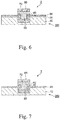
- FIG. 6 is a process drawing schematically showing an example of the step of etching.
- an exposed portion of the copper seed layer 40 on which the metal layer A 70 and the metal layer B 80 are not formed, which is generated by removing the resist pattern, is brought into contact with the etchant of the present invention to etch the exposed portion of the copper seed layer 40.
- a bump 2 having the copper seed layer 40, the copper plating layer 60, the metal layer A 70 and the metal layer B 80, wherein the barrier metal layer 30 is exposed, is formed.
- the bump 2 may be composed of the copper seed layer 40, the metal layer A 60, the copper plating layer 70 and the metal layer B 80. Further, the copper plating layer is not required to be present. In this way, a semiconductor substrate 200 can be produced.
- the temperature of the etchant is not particularly limited, but it is preferably 10 to 50°C, more preferably 20 to 45°C, and even more preferably 25 to 40°C.
- the temperature of the etchant is 10°C or higher, a satisfactory etching rate is obtained, and therefore an excellent production efficiency is obtained.
- the temperature of the etchant is 50°C or lower, it is possible to suppress change in a liquid composition and to keep etching conditions constant.
- the etching rate is increased by increasing the temperature of the etchant, but the optimum treatment temperature may be suitably determined in consideration of suppression of composition change of the etchant (decomposition of hydrogen peroxide), etc.
- the etching treatment time is not particularly limited, but it is preferably 20 to 240 seconds, and more preferably 30 to 120 seconds.
- the treatment time may be suitably selected depending on various conditions including surface conditions of an object to be etched, the concentration and temperature of the etchant and the treatment method.
- the barrier metal layer is removed according to need.
- Figure 7 is a process drawing schematically showing an example of the step of removing a barrier metal layer.
- a bump 3 having the barrier metal layer 30, the copper seed layer 40, the copper plating layer 60, the metal layer A 70 and the metal layer B 80 can be formed.
- the bump 3 may be composed of the barrier metal layer 30, the copper seed layer 40, the metal layer A 60, the copper plating layer 70 and the metal layer B 80.
- the copper plating layer is not required to be present. In this way, the semiconductor substrate 200 can be produced.
- the method for removing the barrier metal layer is not particularly limited, and a publicly-known method can be used.
- the semiconductor substrate produced in the above-described manner is suitably used for TSV (Through Silicon Via) typified by next-generation DRAM memories and NAND memories, etc.
- An etchant was prepared in a manner similar to that in the above-described Examples, except that the composition described in Table 2 was used.
- a substrate having the structure of Figure 5 was used as a substrate for evaluation.
- a titanium layer was used.
- a nickel layer was used.
- a copper plating layer was used.
- a gold layer was used in Example 14
- a tin-silver alloy layer was used in Example 15
- a tin layer was used in Examples 1-13 and Comparative Examples 1-9 (other than Examples 14 and 15).
- the pH value of each etchant prepared in the Examples and Comparative Examples was measured at 25°C using a pH/ION meter of HORIBA, Ltd. (pH meter "D-53" manufactured by HORIBA, Ltd.), wherein an electrode was immersed in the etchant while stirring.
- the pH value of the pH measurement apparatus was adjusted using a standard solution having a pH of 4 or 7.
- the substrate for evaluation was subjected to the etching treatment using each etchant prepared in the Examples and Comparative Examples.
- the substrate for evaluation was immersed in the etchant while stirring at a stirring rate of 200 rpm at 30°C or 40°C, and the time that elapsed before the copper seed layer having a thickness of 600 ⁇ m was dissolved and the titanium layer appeared was measured, thereby evaluating the etching time (just etching time) of the copper seed layer.
- the just etching time (sec) was evaluated based on the below-described criteria.
- the evaluation criteria were as described below. E and G are regarded as acceptable.
- the bump in the substrate for evaluation or the substrate after the etching treatment described in (2) above was cut using a focused ion beam processing device "FB2200" manufactured by Hitachi High-Technologies Corporation.
- the obtained cross section was observed using a scanning electron microscope "S3400N” manufactured by Hitachi High-Technologies Corporation with a magnification of 3,000-fold (acceleration voltage: 5.0 kV, emission current: 30 ⁇ A), and the presence or absence of corrosion with respect to nickel, tin, gold and tin-silver alloy was confirmed.
- the evaluation criteria were as described below. E is regarded as acceptable.
- the etchant of the present invention can be suitably used for wiring formation of a semiconductor substrate in which a bump is used.
- copper and a copper alloy can be selectively etched while suppressing dissolution of wiring materials including nickel, a nickel alloy, tin, a tin alloy, gold and a gold alloy.
Landscapes
- Chemical & Material Sciences (AREA)
- Engineering & Computer Science (AREA)
- Chemical Kinetics & Catalysis (AREA)
- General Chemical & Material Sciences (AREA)
- Materials Engineering (AREA)
- Mechanical Engineering (AREA)
- Metallurgy (AREA)
- Organic Chemistry (AREA)
- ing And Chemical Polishing (AREA)
- Weting (AREA)
- Manufacturing & Machinery (AREA)
Abstract
Description
- The present invention relates to an etchant for selectively etching at least one selected from the group consisting of copper and a copper alloy and a method for producing a semiconductor substrate using the same.
- For wiring formation of a semiconductor substrate in which a bump such as TSV (Through Silicon Via) is used typified by next-generation DRAM memories and NAND memories, it is required to use a technique of selectively etching copper and a copper alloy while suppressing dissolution of nickel, a nickel alloy, tin, a tin alloy, gold and a gold alloy.
- Techniques of selectively etching copper and a copper alloy while suppressing dissolution of nickel and a nickel alloy are known (e.g., Patent Literatures 1-3).
- However, regarding the case where tin, gold and an alloy thereof are included as wiring materials in addition to nickel and a nickel alloy, a technique of selectively etching copper and a copper alloy while suppressing dissolution of these metals has not been examined.
- For example,
Patent Literature 1 discloses an etchant containing hydrogen peroxide and nitric acid at a predetermined concentration ratio. However, in the case where tin and gold are included as wiring materials, dissolution of nickel cannot be prevented when using this etchant. -
- Patent Literature 1:
Japanese Laid-Open Patent Publication No. 2004-43895 - Patent Literature 2:
International Publication WO2011/074589 pamphlet - Patent Literature 3:
International Publication WO2017/188108 pamphlet - Under the above-described circumstances, it has been desired to provide an etchant, wherein, when at least one selected from the group consisting of nickel and a nickel alloy and at least one selected from the group consisting of tin, a tin alloy, gold and a gold alloy are included as wiring materials, copper and a copper alloy can be selectively etched while suppressing dissolution of these metals, and which can be suitably used for wiring formation of a semiconductor substrate in which a bump is used.
- The present inventors diligently made researches with respect to the above-described problem and found that it can be solved by an etchant having a specific composition described below.
- Specifically, the present invention provides an etchant, a method for producing a semiconductor substrate, etc. described below.
- [1] An etchant for selectively etching at least one selected from the group consisting of copper and a copper alloy in a semiconductor substrate that comprises: said at least one selected from the group consisting of copper and the copper alloy; at least one selected from the group consisting of nickel and a nickel alloy; and at least one selected from the group consisting of tin, a tin alloy, gold and a gold alloy, the etchant comprising:
- (A) 5 to 10.5% by mass of hydrogen peroxide relative to the total mass of the etchant;
- (B) 0.3 to 6% by mass of nitric acid relative to the total mass of the etchant;
- (C) at least one nitrogen-containing 5-membered ring compound selected from the group consisting of triazoles and tetrazoles, which may have at least one substituent selected from the group consisting of a C1-6 alkyl group, an amino group, and a substituted amino group having at least one substituent selected from the group consisting of a C1-6 alkyl group and a phenyl group; and
- (D) (d1) at least one pH adjuster selected from the group consisting of an alkali metal hydroxide, ammonia, an amine, and an ammonium salt, (d2) a phosphonic acid compound, or (d3) a combination of (d1) and (d2).
- [2] The etchant according to item [1], wherein the component (C) is at least one nitrogen-containing 5-membered ring compound selected from the group consisting of 5-methyltetrazole, 5-aminotetrazole and 1,2,4-triazole.
- [3] The etchant according to item [1] or [2], wherein the concentration of the component (C) is 0.005 to 2.0% by mass relative to the total mass of the etchant.
- [4] The etchant according to any one of items [1] to [3], having a pH of 0.5 to 3.0.
- [5] The etchant according to any one of items [1] to [3], comprising (d2) the phosphonic acid compound.
- [6] The etchant according to any one of items [1] to [5], wherein the component (d2) is at least one phosphonic acid compound selected from the group consisting of 1-hydroxyethylidene-1,1-diphosphonic acid, diethylenetriaminepenta(methylenephosphonic acid) and a salt thereof.
- [7] The etchant according to any one of items [1] to [6], wherein the concentration of the component (d2) is 0.005 to 1.0% by mass relative to the total mass of the etchant.
- [8] A method for producing a semiconductor substrate, comprising:
- a step of preparing a semiconductor base material having, on its surface, a copper seed layer containing at least one selected from the group consisting of copper and a copper alloy;
- a step of forming a resist pattern having an opening pattern, wherein the copper seed layer is partially exposed;
- a step of forming a metal layer A containing at least one selected from the group consisting of nickel and a nickel alloy and a metal layer B containing at least one selected from the group consisting of tin, a tin alloy, gold and a gold alloy to be arranged in this order on the surface of the copper seed layer exposed at an opening of the opening pattern of the resist pattern;
- a step of removing the resist pattern; and
- a step of bringing an exposed portion of the copper seed layer on which the metal layer A and the metal layer B are not formed, which is generated by removing the resist pattern, into contact with the etchant according to any one of items [1] to [7] to etch the exposed portion of the copper seed layer.
- [9] The method for producing the semiconductor substrate according to item [8], wherein a bump comprising the metal layer A containing at least one selected from the group consisting of nickel and the nickel alloy and the metal layer B containing at least one selected from the group consisting of tin, the tin alloy, gold and the gold alloy is formed on the semiconductor base material.
- According to the present invention, an etchant for selectively etching copper and a copper alloy can be provided. Further, according to the present invention, a method for producing a semiconductor substrate using the etchant can be provided.
- According to a preferred embodiment of the present invention, by using the etchant, copper and a copper alloy can be selectively etched while suppressing dissolution of nickel, a nickel alloy, tin, a tin alloy, gold and a gold ally. Further, according to a preferred embodiment of the present invention, the etchant can be suitably used for wiring formation of a semiconductor substrate in which a bump is used.
-
-
FIG. 1(a) to FIG. 1(c) are process drawings schematically showing an example of the step of preparing a base material. -
FIG. 2 is a process drawing schematically showing an example of the step of forming a resist pattern. -
FIG. 3 is a process drawing schematically showing an example of the step of forming a copper plating layer. -
FIG. 4 is a process drawing schematically showing an example of the step of forming metal layers. -
FIG. 5 is a process drawing schematically showing an example of the step of removing a resist pattern. -
FIG. 6 is a process drawing schematically showing an example of the step of etching. -
FIG. 7 is a process drawing schematically showing an example of the step of removing a barrier metal layer. - Hereinafter, the etchant, the method for producing a semiconductor substrate, etc. of the present invention will be specifically described, but the present invention is not limited thereto and can be variously modified within a range not departing from the gist of the present invention.
- The etchant of the present invention is characterized in that it is an etchant for selectively etching at least one selected from the group consisting of copper and a copper alloy in a semiconductor substrate that comprises: said at least one selected from the group consisting of copper and the copper alloy; at least one selected from the group consisting of nickel and a nickel alloy; and at least one selected from the group consisting of tin, a tin alloy, gold and a gold alloy, and that the etchant comprises:
- (A) 5 to 10.5% by mass of hydrogen peroxide relative to the total mass of the etchant;
- (B) 0.3 to 6% by mass of nitric acid relative to the total mass of the etchant;
- (C) at least one nitrogen-containing 5-membered ring compound selected from the group consisting of triazoles and tetrazoles, which may have at least one substituent selected from the group consisting of a C1-6 alkyl group, an amino group, and a substituted amino group having at least one substituent selected from the group consisting of a C1-6 alkyl group and a phenyl group; and
- (D) (d1) at least one pH adjuster selected from the group consisting of an alkali metal hydroxide, ammonia, an amine, and an ammonium salt, (d2) a phosphonic acid compound, or (d3) a combination of (d1) and (d2).
- According to a preferred embodiment of the present invention, the etchant of the present invention contains a specific component at a specific ratio as described above, and because of this, when at least one selected from the group consisting of nickel and a nickel alloy and at least one selected from the group consisting of tin, a tin alloy, gold and a gold alloy are included as wiring materials, copper and a copper alloy can be selectively etched while suppressing dissolution of the above-described metals. Note that in this specification, the "nickel alloy" is a material obtained by adding at least one metallic element or non-metallic element to nickel and is not particularly limited as long as it has a metallic property. The same applies to the "tin alloy", the "gold alloy" and the "copper alloy".
- Hereinafter, respective components contained in the etchant of the present invention will be described in detail.
- In the present invention, hydrogen peroxide (A) (hereinafter also referred to as "the component (A)") is a component that functions as an oxidant for copper.
- The grade of hydrogen peroxide (A) is not particularly limited, and hydrogen peroxides with various grades such as industrial/electronics industrial grade can be used. In general, hydrogen peroxide (A) is preferably used in the form of an aqueous hydrogen peroxide solution in view of availability and operability.
- The concentration of hydrogen peroxide (A) in the etchant is 5 to 10.5% by mass, and preferably 6.0 to 10.0% by mass relative to the total mass of the etchant. When the concentration of hydrogen peroxide (A) is within the above-described range, a satisfactory etching rate is obtained. In addition, dissolution of wiring materials can be suppressed.
- In the present invention, nitric acid (B) (hereinafter also referred to as "the component (B)") is a component that acts as an etchant for copper and the copper alloy oxidized by hydrogen peroxide.
- The concentration of nitric acid (B) in the etchant is 0.3 to 6% by mass, preferably 0.5 to 5.0% by mass, and more preferably 1.0 to 4.0% by mass. When the concentration of nitric acid (B) is within the above-described range, a satisfactory etching rate is obtained. In addition, dissolution of wiring materials can be suppressed.
- In the present invention, it is considered that the nitrogen-containing 5-membered ring compound (C) (hereinafter also referred to as "the component (C)") has a function to adsorb to the copper surface to control the etching rate of copper and to reduce corrosion of nickel and tin.
- The nitrogen-containing 5-membered ring compound (C) is at least one selected from the group consisting of triazoles and tetrazoles, which may have at least one substituent selected from the group consisting of a C1-6 alkyl group, an amino group, and a substituted amino group having at least one substituent selected from the group consisting of a C1-6 alkyl group and a phenyl group. As the nitrogen-containing 5-membered ring compound (C), one material may be used solely, or two or more materials may be used in combination.
- Preferred examples of the nitrogen-containing 5-membered ring compound (C) include a compound represented by formula (1), formula (2) or formula (3):

- Examples of the C1-6 alkyl group include a linear or branched alkyl group and a cycloalkyl group. Examples of the linear or branched alkyl group include a methyl group, an ethyl group, an n-propyl group, an isopropyl group, an n-butyl group, an isobutyl group, a sec-butyl group, a tert-butyl group, an n-pentyl group and an n-hexyl group. Examples of the cycloalkyl group include a C3-6 cycloalkyl group, and examples thereof include a cyclopropyl group, a cyclopentyl group and a cyclohexyl group. Among them, a methyl group or an ethyl group is preferred, and a methyl group is particularly preferred.
- The substituted amino group is not particularly limited as long as it is an amino group having at least one substituent selected from the group consisting of a C1-6 alkyl group and a phenyl group. The C1-6 alkyl group is as explained with examples above.
- Preferred specific examples of the nitrogen-containing 5-membered ring compound (C) include 5-methyltetrazole, 5-aminotetrazole, 1,2,4-triazole, 1,2,3-triazole and tetrazole. Among them, at least one selected from the group consisting of 5-methyltetrazole, 5-aminotetrazole and 1,2,4-triazole is particularly preferred.
- The concentration of the nitrogen-containing 5-membered ring compound (C) in the etchant is preferably 0.005 to 2.0% by mass, more preferably 0.01 to 1.0% by mass, and even more preferably 0.05 to 0.5% by mass relative to the total mass of the etchant. When the concentration of the nitrogen-containing 5-membered ring compound (C) is within the above-described range, a satisfactory etching rate is obtained. In addition, dissolution of wiring materials can be suppressed.
- In the present invention, as the component (D), (d1) at least one pH adjuster selected from the group consisting of an alkali metal hydroxide, ammonia, an amine, and an ammonium salt, (d2) a phosphonic acid compound or (d3) a combination of (d1) and (d2) is contained. When the component (D) is contained, dissolution of wiring materials can be suppressed.
- The component (d1) is at least one pH adjuster selected from the group consisting of an alkali metal hydroxide, ammonia, an amine and an ammonium salt. When the component (d1) is contained, the pH of the etchant can be adjusted to be within an appropriate range.
- The pH range of the etchant of the present invention is not particularly limited, but it is preferably 0.5 to 3.0, more preferably 0.6 to 3.0, even more preferably 0.7 to 2.0, particularly preferably 0.7 to 1.6, and most preferably 0.7 to 1.3. However, this is not applied to the case where the etchant of the present invention contains the component (d2) described later, and in this case, even when the pH range of the etchant is not within the above-described range, dissolution of wiring materials can be effectively suppressed.
- The alkali metal hydroxide is not particularly limited as long as it is a hydroxide of an alkali metal, and examples thereof include potassium hydroxide, sodium hydroxide, lithium hydroxide and cesium hydroxide.
- The amine is not particularly limited as long as it is a compound in which hydrogen atoms of ammonia are substituted with 1 to 3 organic groups, and examples thereof include: alkanolamines such as monoethanolamine, diethanolamine, triethanolamine, diethyleneglycolamine, 1-amino-2-propanol and N-hydroxylethylpiperazine; and organic amines not having a hydroxyl group such as ethylamine, benzylamine, diethylamine, n-butylamine, 3-methoxypropylamine, tert-butylamine, n-hexylamine, cyclohexylamine, n-octylamine, 2-ethylhexylamine, o-xylylenediamine, m-xylylenediamine, 1-methylbutylamine, ethylenediamine, 1,3-propanediamine, 2-aminobenzylamine, N-benzylethylenediamine, diethylenetriamine and triethylenetetramine.
- The ammonium salt is not particularly limited as long as it is a water-soluble quaternary ammonium salt. Examples thereof include alkaline quaternary ammonium salts such as tetramethylammonium hydroxide, ethyltrimethylammonium hydroxide and tetraethylammonium hydroxide.
- As the pH adjuster, for example, potassium hydroxide, sodium hydroxide, lithium hydroxide, cesium hydroxide, triethylamine, ammonia, tetramethylammonium hydroxide, ethanolamine, 1-amino-2-propanol, etc. can be preferably used. As the pH adjuster, one of such materials may be used solely, or two or more of them may be used in combination.
- The component (d2) is a phosphonic acid compound. As described above, in the case where the component (d2) is contained, even when the pH range of the etchant is not adjusted within a predetermined range, expected effects can be obtained.
- Examples of the phosphonic acid compound include 1-hydroxyethylidene-1,1-diphosphonic acid (HEDP), aminotri(methylenephosphonic acid) (ATP), ethylenediaminetetra(methylenephosphonic acid) (EDTP), cis-cyclohexanediaminetetra(methylenephosphonic acid) (cis-CDTP), trans-cyclohexanediaminetetra(methylenephosphonic acid) (trans-CDTP), hexamethylenediaminetetra(methylenephosphonic acid) (HDTP), diethylenetriaminepenta(methylenephosphonic acid) (DTPP), triethylenetetraminehexa(methylenephosphonic acid) (TTHP), tri(2-aminoethyl)aminehexa(methylenephosphonic acid) (TAEHP), tetraethylenepentaminehepta(methylenephosphonic acid) (TPHP), pentaethylenehexamineocta(methylenephosphonic acid) (PHOP) and a salt thereof. Among them, at least one phosphonic acid compound selected from the group consisting of 1-hydroxyethylidene-1,1-diphosphonic acid (HEDP), diethylenetriaminepenta(methylenephosphonic acid) (DTPP) and a salt thereof is preferred, and at least one phosphonic acid compound selected from the group consisting of 1-hydroxyethylidene-1,1-diphosphonic acid (HEDP) and a salt thereof is particularly preferred. As the phosphonic acid compound, one of such materials may be used solely, or two or more of them may be used in combination.
- The concentration of the component (d2) is preferably 0.005 to 1.0% by mass, more preferably 0.075 to 0.5% by mass, and particularly preferably 0.01 to 0.1% by mass relative to the total mass of the etchant.
- The etchant of the present invention may contain a combination of the component (d1) and the component (d2). In this case, it is sufficient when the concentrations of the component (d1) and the component (d2) are respectively within the above-described ranges, and the pH range may be outside the above-described range.
- In addition to the component (A), the component (B), the component (C) and the component (D), the etchant of the present invention may contain water, and according to need, at least one of additives usually used for other etchants within a range not impairing the effects of the etchant of the present invention.
- Water is preferably water from which metal ions, organic impurities, particles, etc. have been removed by distillation, ion exchange treatment, filtering treatment, adsorption treatment or the like. Pure water is more preferred, and ultrapure water is particularly preferred.
- Further, to the etchant of the present invention, a publicly-known hydrogen peroxide stabilizer such as alcohols, urea, phenylurea and organic carboxylic acids, an etching rate adjuster, etc. may be added according to need.
- Note that the etchant of the present invention is preferably a solution and does not contain solid particles such as abrasive particles.
- In the etchant of the present invention, the total content of the component (A), the component (B), the component (C), the component (D) and water is preferably 70 to 100% by mass, more preferably 85 to 100% by mass, even more preferably 90 to 100% by mass, and particularly preferably 95 to 100% by mass relative to the total mass of the etchant.
- The etchant of the present invention can be prepared by homogeneously stirring the component (A), the component (B), the component (C), the component (D) and water, and according to need, other components. The method for stirring these components is not particularly limited, and a stirring method usually used for preparing an etchant can be employed.
- The etchant of the present invention can be used for etching copper and a copper alloy. In particular, at the time of wiring formation of a semiconductor substrate in which a bump such as TSV (Through Silicon Via) is used typified by next-generation DRAM memories and NAND memories, when at least one selected from the group consisting of nickel and a nickel alloy and at least one selected from the group consisting of tin, a tin alloy, gold and a gold alloy are contained as wiring materials, the etchant of the present invention can be suitably used as an etchant for selectively etching at least one selected from copper and a copper alloy while suppressing dissolution of the above-described metals.
- The temperature of the etchant of the present invention at the time of use is not particularly limited, but it is preferably 10 to 50°C, more preferably 20 to 45°C, and even more preferably 25 to 40°C. When the temperature of the etchant is 10°C or higher, a satisfactory etching rate is obtained, and therefore an excellent production efficiency is obtained. Meanwhile, when the temperature of the etchant is 50°C or lower, it is possible to suppress change in a liquid composition and to keep etching conditions constant. The etching rate is increased by increasing the temperature of the etchant, but the optimum treatment temperature may be suitably determined in consideration of suppression of composition change of the etchant (decomposition of hydrogen peroxide), etc.
- Further, the etching treatment time is not particularly limited, but it is preferably 20 to 240 seconds, and more preferably 30 to 120 seconds. The treatment time may be suitably selected depending on various conditions including surface conditions of an object to be etched, the concentration and temperature of the etchant and the treatment method.
- The method for bringing an object to be etched into contact with the etchant is not particularly limited. For example, it is possible to employ a wet etching method such as a method of bringing the object to be etched into contact with the etchant by means of dropping (single wafer spin process), spray or the like, or a method of immersing the object to be etched in the etchant. In the present invention, any of such methods may be employed.
- The method for producing a semiconductor substrate of the present invention is characterized in that it comprises:
- a step of preparing a semiconductor base material having, on its surface, a copper seed layer containing at least one selected from the group consisting of copper and a copper alloy;
- a step of forming a resist pattern having an opening pattern, wherein the copper seed layer is partially exposed;
- a step of forming a metal layer A containing at least one selected from the group consisting of nickel and a nickel alloy and a metal layer B containing at least one selected from the group consisting of tin, a tin alloy, gold and a gold alloy to be arranged in this order on the surface of the copper seed layer exposed at an opening of the opening pattern of the resist pattern;
- a step of removing the resist pattern; and
- a step of bringing an exposed portion of the copper seed layer on which the metal layer A and the metal layer B are not formed, which is generated by removing the resist pattern, into contact with the etchant of the present invention to etch the exposed portion of the copper seed layer.
- Hereinafter, an example of the method for producing a semiconductor substrate of the present invention will be described based on drawings.
- In the step of preparing a base material, a semiconductor base material having, on its surface, a copper seed layer containing at least one selected from the group consisting of copper and a copper alloy is prepared.
-
Figure 1(a) to Figure 1(c) are process drawings schematically showing an example of the step of preparing a base material. - Firstly, as shown in
Figure 1(a) , asilicon substrate 10 having aplane portion 11 is prepared. - Next, as shown in
Figure 1(b) , arecess 12 composed of a bottom 12a and aside 12b is formed in theplane portion 11 of thesilicon substrate 10. The method for forming therecess 12 is not particularly limited, and an ordinary method such as a laser processing method and a drilling method can be employed. - Next, as shown in
Figure 1(c) , acopper seed layer 40 is formed on the surfaces of theplane portion 11 and the bottom 12a and theside 12b of therecess 12 of thesilicon substrate 10. Optionally, before forming thecopper seed layer 40, asilicon oxide layer 20 may be formed and abarrier metal layer 30 such as a titanium layer may be formed thereon, and then thecopper seed layer 40 may be formed thereon or another layer may be further added. In this way, in therecess 12, thecopper seed layer 40 is formed, or thesilicon oxide layer 20, thebarrier metal layer 30 and thecopper seed layer 40 are formed in this order, and as a result, aconcave portion 1 having a bottom 1a and aside 1b which are composed of thecopper seed layer 40 is formed. In this way, asemiconductor base material 100 having thecopper seed layer 40 on its surface, wherein theconcave portion 1 is formed, can be prepared. The method for forming the silicon oxide layer, the copper seed layer and the barrier metal layer is not particularly limited, and a publicly-known method can be used. For example, regarding the copper seed layer and the barrier metal layer, a sputtering method is preferably used. - Next, a resist pattern having an opening pattern, wherein the copper seed layer obtained in the aforementioned step is partially exposed, is formed.
-
Figure 2 is a process drawing schematically showing an example of the step of forming a resist pattern. - As shown in
Figure 2 , a resist pattern is formed by forming a resistresin layer 50 on the surface of thecopper seed layer 40 in a manner such that a part of the surface of thecopper seed layer 40 from the edge toward the outside of theconcave portion 1 is exposed. The method for forming the resist pattern is not particularly limited, and a publicly-known method can be used. For example, the resist pattern can be formed by exposing a pattern to light using a liquid resist or a dry film resist. - Next, a metal layer A containing at least one selected from the group consisting of nickel and a nickel alloy and a metal layer B containing at least one selected from the group consisting of tin, a tin alloy, gold and a gold alloy are formed to be arranged in this order on the surface of the copper seed layer exposed at an opening of the opening pattern of the resist pattern formed in the aforementioned step.
-
Figure 3 is a process drawing schematically showing an example of the step of forming a copper plating layer. As shown inFigure 3 , optionally, before forming the metal layers A and B, acopper plating layer 60 may be formed by performing copper plating in a manner such that theconcave portion 1 is filled and the exposed portion of thecopper seed layer 40 is covered. -
Figure 4 is a process drawing schematically showing an example of the step of forming metal layers. As shown inFigure 4 , ametal layer A 70 and ametal layer B 80 are formed to be arranged in this order on the surface of thecopper plating layer 60. - In another embodiment of the present invention, the copper plating layer and the metal layer A may be arranged in reverse order, and a
metal layer A 60 may be formed in a manner such that theconcave portion 1 is filled and the exposed portion of thecopper seed layer 40 is covered, and acopper plating layer 70 and ametal layer B 80 may be formed to be arranged in this order on the surface of themetal layer A 60. - Further, it is not necessary to form a copper plating layer. In the case where no copper plating layer is formed, the
metal layer A 70 and themetal layer B 80 are formed to be arranged in this order on the exposed portion of thecopper seed layer 40. As each of the metal layer A and the metal layer B, one layer or two or more layers may be formed. Further, another layer may be formed between the metal layer A and the metal layer B or next to the metal layer A or the metal layer B. The method for forming the copper plating layer, the metal layer A, the metal layer B, etc. is not particularly limited, and a publicly-known method can be used. For example, electrolytic plating is preferably used. -
Figure 5 is a process drawing schematically showing an example of the step of removing a resist pattern. As shown inFigure 5 , the resistresin layer 50 is removed. The method for removing the resist resin layer is not particularly limited, and a publicly-known method can be used. -
Figure 6 is a process drawing schematically showing an example of the step of etching. As shown inFigure 6 , an exposed portion of thecopper seed layer 40 on which themetal layer A 70 and themetal layer B 80 are not formed, which is generated by removing the resist pattern, is brought into contact with the etchant of the present invention to etch the exposed portion of thecopper seed layer 40. In this way, a bump 2 having thecopper seed layer 40, thecopper plating layer 60, themetal layer A 70 and themetal layer B 80, wherein thebarrier metal layer 30 is exposed, is formed. Note that the bump 2 may be composed of thecopper seed layer 40, themetal layer A 60, thecopper plating layer 70 and themetal layer B 80. Further, the copper plating layer is not required to be present. In this way, asemiconductor substrate 200 can be produced. - The temperature of the etchant is not particularly limited, but it is preferably 10 to 50°C, more preferably 20 to 45°C, and even more preferably 25 to 40°C. When the temperature of the etchant is 10°C or higher, a satisfactory etching rate is obtained, and therefore an excellent production efficiency is obtained. Meanwhile, when the temperature of the etchant is 50°C or lower, it is possible to suppress change in a liquid composition and to keep etching conditions constant. The etching rate is increased by increasing the temperature of the etchant, but the optimum treatment temperature may be suitably determined in consideration of suppression of composition change of the etchant (decomposition of hydrogen peroxide), etc.
- The etching treatment time is not particularly limited, but it is preferably 20 to 240 seconds, and more preferably 30 to 120 seconds. The treatment time may be suitably selected depending on various conditions including surface conditions of an object to be etched, the concentration and temperature of the etchant and the treatment method.
- After the step of etching, the barrier metal layer is removed according to need.
-
Figure 7 is a process drawing schematically showing an example of the step of removing a barrier metal layer. As shown inFigure 7 , by removing the exposed portion of thebarrier metal layer 30, abump 3 having thebarrier metal layer 30, thecopper seed layer 40, thecopper plating layer 60, themetal layer A 70 and themetal layer B 80 can be formed. Note that thebump 3 may be composed of thebarrier metal layer 30, thecopper seed layer 40, themetal layer A 60, thecopper plating layer 70 and themetal layer B 80. Further, the copper plating layer is not required to be present. In this way, thesemiconductor substrate 200 can be produced. The method for removing the barrier metal layer is not particularly limited, and a publicly-known method can be used. - In the above-described manner, it is possible to produce a semiconductor substrate, in which a bump comprising a metal layer A containing at least one selected from the group consisting of nickel and a nickel alloy and a metal layer B containing at least one selected from the group consisting of tin, a tin alloy, gold and a gold alloy is formed. According to a preferred embodiment of the present invention, the semiconductor substrate produced in the above-described manner is suitably used for TSV (Through Silicon Via) typified by next-generation DRAM memories and NAND memories, etc.
- Hereinafter, the present invention will be specifically described based on working examples, but embodiments can be suitably changed within a range in which the effects of the present invention are exerted.
- Using the composition described in Table 1, hydrogen peroxide (A); nitric acid (B); a nitrogen-containing 5-membered ring compound (C); a pH adjuster (d1), a phosphonic acid compound (d2) or a combination thereof (d3); and pure water were put into a glass beaker having a capacity of 1 L, and the mixture was stirred to be homogeneous to prepare an etchant. Note that the amount of the pH adjuster to be added was determined in a manner such that a desired pH was obtained when mixing all the materials.
- An etchant was prepared in a manner similar to that in the above-described Examples, except that the composition described in Table 2 was used.
- A substrate having the structure of
Figure 5 was used as a substrate for evaluation. As thebarrier metal layer 30, a titanium layer was used. As themetal layer A 60, a nickel layer was used. As thelayer 70, a copper plating layer was used. As themetal layer B 80, a gold layer was used in Example 14, a tin-silver alloy layer was used in Example 15, and a tin layer was used in Examples 1-13 and Comparative Examples 1-9 (other than Examples 14 and 15). - The pH value of each etchant prepared in the Examples and Comparative Examples was measured at 25°C using a pH/ION meter of HORIBA, Ltd. (pH meter "D-53" manufactured by HORIBA, Ltd.), wherein an electrode was immersed in the etchant while stirring. The pH value of the pH measurement apparatus was adjusted using a standard solution having a pH of 4 or 7.
- The substrate for evaluation was subjected to the etching treatment using each etchant prepared in the Examples and Comparative Examples.
- The substrate for evaluation was immersed in the etchant while stirring at a stirring rate of 200 rpm at 30°C or 40°C, and the time that elapsed before the copper seed layer having a thickness of 600 µm was dissolved and the titanium layer appeared was measured, thereby evaluating the etching time (just etching time) of the copper seed layer.
- For evaluation of corrosion of nickel, tin, gold and tin-silver alloy, an object was immersed for a time that was twice as long as the just etching time, and after that, it was washed with pure water, then dried, and observed using a scanning electron microscope as described later.
- The just etching time (sec) was evaluated based on the below-described criteria. The evaluation criteria were as described below. E and G are regarded as acceptable.
- E: 30 to 120 sec
- G: 20 to 30 sec or 121 to 240 sec
- B: less than 19 sec or more than 241 sec
- The bump in the substrate for evaluation or the substrate after the etching treatment described in (2) above was cut using a focused ion beam processing device "FB2200" manufactured by Hitachi High-Technologies Corporation. The obtained cross section (cross section of the bump) was observed using a scanning electron microscope "S3400N" manufactured by Hitachi High-Technologies Corporation with a magnification of 3,000-fold (acceleration voltage: 5.0 kV, emission current: 30 µA), and the presence or absence of corrosion with respect to nickel, tin, gold and tin-silver alloy was confirmed. The evaluation criteria were as described below. E is regarded as acceptable.
- E: corrosion was not confirmed by means of SEM
- (Decrease in bump diameter before and after treatment: less than 0.5 µm, no abnormalities on metal surface)
- B: corrosion was confirmed by means of SEM
- NE: it was impossible to perform the measurement because the copper seed layer was not etched
- WE: it was impossible to perform the measurement because it was impossible to confirm the presence or absence of a bump due to disappearance of the copper seed layer under the bump
- In the tables, "-" means that the corrosion test was not conducted.
- The evaluation results of the Examples are shown in Table 1, and the evaluation results of the Comparative Examples are shown in Table 2. In the tables, "Remainder" means the content of pure water required when the amount of the etchant is 100% by mass.
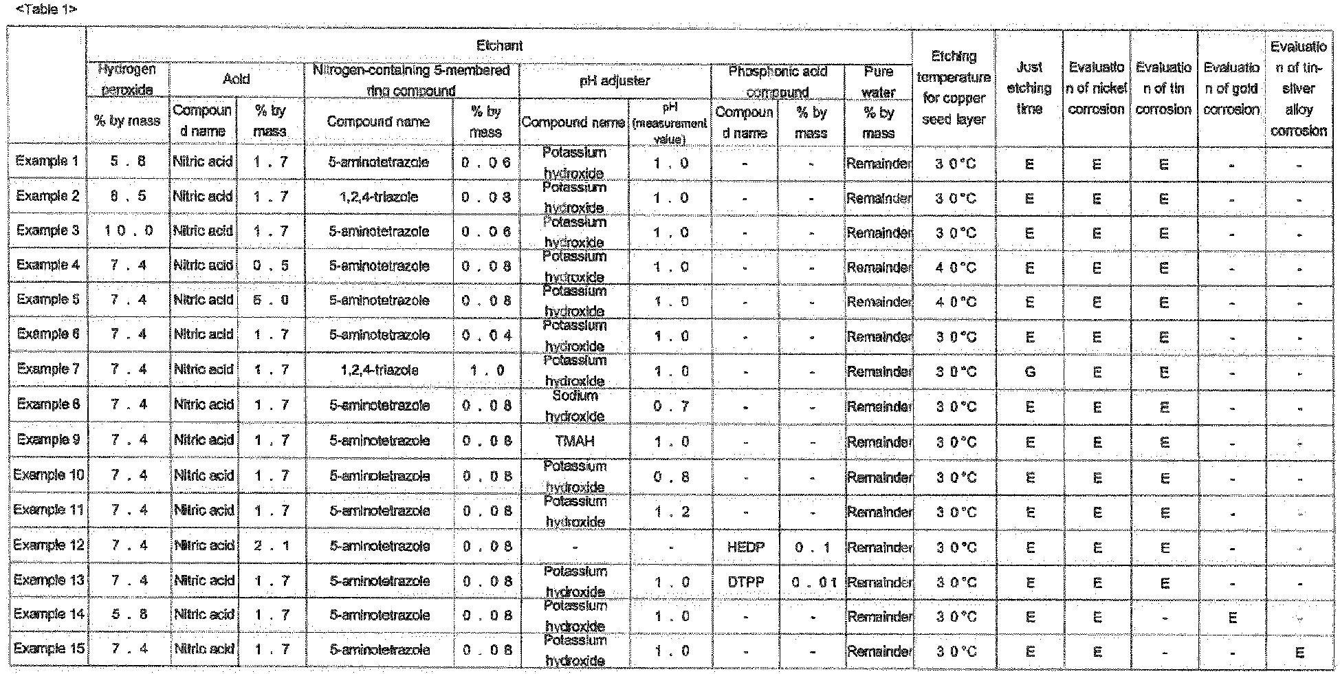

- As shown in Table 1, it was confirmed that copper was selectively etched by each of the etchants of Examples 1-15 successfully while suppressing corrosion of nickel, tin, gold and the tin-silver alloy.
- Meanwhile, as shown in Table 2, when the composition ratio of the component (A) was not within the range defined by the present invention, corrosion of nickel or tin was caused (Comparative Examples 1 and 2). Further, when the composition ratio of the component (B) was not within the range defined by the present invention or the component (B) was not contained, etching of the copper seed layer did not proceed (Comparative Examples 3, 4 and 5).
- It was found that when sulfuric acid was used instead of nitric acid as the component (B), etching of the copper seed layer proceeded, but corrosion of nickel was caused (Comparative Example 6). Further, it was found that when the component (D) was not contained, corrosion of tin was caused (Comparative Example 7).
- When the nitrogen-containing 5-membered ring compound as the component (C) was not used, corrosion of nickel and tin was caused (Comparative Example 8), or etching of the copper seed layer did not proceed and a part or all of the bump collapsed (Comparative Example 9).
- The etchant of the present invention can be suitably used for wiring formation of a semiconductor substrate in which a bump is used. According to a preferred embodiment of the present invention, copper and a copper alloy can be selectively etched while suppressing dissolution of wiring materials including nickel, a nickel alloy, tin, a tin alloy, gold and a gold alloy.
-
- 1
- concave portion
- 1a
- bottom of concave portion
- 1b
- side of concave portion
- 2, 3
- bump
- 10
- silicon substrate
- 11
- plane portion
- 12
- recess
- 12a
- bottom of recess
- 12b
- side of recess
- 20
- silicon oxide layer
- 30
- barrier metal layer
- 40
- copper seed layer
- 50
- resist resin layer
- 60
- copper plating layer or metal layer A
- 70
- metal layer A or copper plating layer
- 80
- metal layer B
- 100
- semiconductor base material
- 200
- semiconductor substrate
Claims (10)
- An etchant for selectively etching at least one selected from the group consisting of copper and a copper alloy in a semiconductor substrate that comprises: said at least one selected from the group consisting of copper and the copper alloy; at least one selected from the group consisting of nickel and a nickel alloy; and at least one selected from the group consisting of tin, a tin alloy, gold and a gold alloy, the etchant comprising:(A) 5 to 10.5% by mass of hydrogen peroxide relative to the total mass of the etchant;(B) 0.3 to 6% by mass of nitric acid relative to the total mass of the etchant;(C) at least one nitrogen-containing 5-membered ring compound selected from the group consisting of triazoles and tetrazoles, which may have at least one substituent selected from the group consisting of a C1-6 alkyl group, an amino group, and a substituted amino group having at least one substituent selected from the group consisting of a C1-6 alkyl group and a phenyl group; and(D) (d1) at least one pH adjuster selected from the group consisting of an alkali metal hydroxide, ammonia, an amine, and an ammonium salt, (d2) a phosphonic acid compound, or (d3) a combination of(d1) and (d2).
- The etchant according to claim 1, wherein the component (C) is at least one nitrogen-containing 5-membered ring compound selected from the group consisting of 5-methyltetrazole, 5-aminotetrazole and 1,2,4-triazole.
- The etchant according to claim 1 or 2, wherein the concentration of the component (C) is 0.005 to 2.0% by mass relative to the total mass of the etchant.
- The etchant according to any one of claims 1 to 3, having a pH of 0.5 to 3.0.
- The etchant according to claim 4, having a pH of 0.7 to 1.3.
- The etchant according to any one of claims 1 to 3, comprising (d2) the phosphonic acid compound.
- The etchant according to any one of claims 1 to 6, wherein the component (d2) is at least one phosphonic acid compound selected from the group consisting of 1-hydroxyethylidene-1,1-diphosphonic acid, diethylenetriaminepenta(methylenephosphonic acid) and a salt thereof.
- The etchant according to any one of claims 1 to 7, wherein the concentration of the component (d2) is 0.005 to 1.0% by mass relative to the total mass of the etchant.
- A method for producing a semiconductor substrate, comprising:a step of preparing a semiconductor base material having, on its surface, a copper seed layer containing at least one selected from the group consisting of copper and a copper alloy;a step of forming a resist pattern having an opening pattern, wherein the copper seed layer is partially exposed;a step of forming a metal layer A containing at least one selected from the group consisting of nickel and a nickel alloy and a metal layer B containing at least one selected from the group consisting of tin, a tin alloy, gold and a gold alloy to be arranged in this order on the surface of the copper seed layer exposed at an opening of the opening pattern of the resist pattern;a step of removing the resist pattern; anda step of bringing an exposed portion of the copper seed layer on which the metal layer A and the metal layer B are not formed, which is generated by removing the resist pattern, into contact with the etchant according to any one of claims 1 to 8 to etch the exposed portion of the copper seed layer.
- The method for producing the semiconductor substrate according to claim 9, wherein a bump comprising the metal layer A containing at least one selected from the group consisting of nickel and the nickel alloy and the metal layer B containing at least one selected from the group consisting of tin, the tin alloy, gold and the gold alloy is formed on the semiconductor base material.
Applications Claiming Priority (2)
| Application Number | Priority Date | Filing Date | Title |
|---|---|---|---|
| JP2018217067 | 2018-11-20 | ||
| PCT/JP2019/045158 WO2020105605A1 (en) | 2018-11-20 | 2019-11-19 | Etchant for selectively etching copper and copper alloy, and method for manufacturing semiconductor substrate using said etchant |
Publications (3)
| Publication Number | Publication Date |
|---|---|
| EP3885468A1 true EP3885468A1 (en) | 2021-09-29 |
| EP3885468A4 EP3885468A4 (en) | 2022-01-05 |
| EP3885468B1 EP3885468B1 (en) | 2024-08-14 |
Family
ID=70773324
Family Applications (1)
| Application Number | Title | Priority Date | Filing Date |
|---|---|---|---|
| EP19886247.6A Active EP3885468B1 (en) | 2018-11-20 | 2019-11-19 | Etchant for selectively etching copper and copper alloy, and method for manufacturing semiconductor substrate using said etchant |
Country Status (7)
| Country | Link |
|---|---|
| US (1) | US11821092B2 (en) |
| EP (1) | EP3885468B1 (en) |
| JP (1) | JP7367700B2 (en) |
| KR (1) | KR102811310B1 (en) |
| CN (1) | CN113015823B (en) |
| TW (1) | TWI831869B (en) |
| WO (1) | WO2020105605A1 (en) |
Families Citing this family (1)
| Publication number | Priority date | Publication date | Assignee | Title |
|---|---|---|---|---|
| KR20250103640A (en) | 2022-11-01 | 2025-07-07 | 미쯔비시 가스 케미칼 컴파니, 인코포레이티드 | Aqueous composition for etching, etching method using the same, and method for manufacturing semiconductor substrate |
Family Cites Families (16)
| Publication number | Priority date | Publication date | Assignee | Title |
|---|---|---|---|---|
| JP3968554B2 (en) * | 2000-05-01 | 2007-08-29 | セイコーエプソン株式会社 | Bump forming method and semiconductor device manufacturing method |
| JP2004043895A (en) | 2002-07-12 | 2004-02-12 | Mitsubishi Chemicals Corp | Copper etchant |
| JP5794147B2 (en) | 2009-12-15 | 2015-10-14 | 三菱瓦斯化学株式会社 | Etching solution and method of manufacturing semiconductor device using the same |
| WO2011093445A1 (en) * | 2010-01-28 | 2011-08-04 | 三菱瓦斯化学株式会社 | Etching liquid for a copper/titanium multilayer thin film |
| KR101271414B1 (en) | 2010-02-15 | 2013-06-05 | 미쯔비시 가스 케미칼 컴파니, 인코포레이티드 | Etching solution for multilayer thin film having copper layer and molybdenum layer contained therein |
| JP6101421B2 (en) * | 2010-08-16 | 2017-03-22 | インテグリス・インコーポレーテッド | Etching solution for copper or copper alloy |
| KR101901721B1 (en) * | 2011-07-26 | 2018-09-28 | 미쯔비시 가스 케미칼 컴파니, 인코포레이티드 | Etchant for copper/molybdenum-based multilayer thin film |
| JP5933950B2 (en) * | 2011-09-30 | 2016-06-15 | アドバンスド テクノロジー マテリアルズ,インコーポレイテッド | Etching solution for copper or copper alloy |
| JP2014101561A (en) * | 2012-11-21 | 2014-06-05 | Sanyo Chem Ind Ltd | Etching solution for copper or copper alloy |
| TWI600129B (en) | 2013-05-06 | 2017-09-21 | 奇景光電股份有限公司 | Glass flip-chip bonding structure |
| JP6128404B2 (en) | 2013-11-25 | 2017-05-17 | パナソニックIpマネジメント株式会社 | Etching solution for multilayer film, etching concentrated solution, and etching method |
| KR102255577B1 (en) * | 2014-08-25 | 2021-05-25 | 엘지디스플레이 주식회사 | Etching composition |
| JP6494254B2 (en) * | 2014-11-18 | 2019-04-03 | 関東化學株式会社 | Copper / molybdenum metal laminated film etching solution composition, etching method using the composition, and method for extending the life of the composition |
| JP6531612B2 (en) * | 2014-11-27 | 2019-06-19 | 三菱瓦斯化学株式会社 | Liquid composition and etching method using the same |
| CN108699706B (en) | 2016-04-27 | 2021-01-01 | 三洋化成工业株式会社 | Etching solution and method for manufacturing electronic substrate |
| CN108570678B (en) * | 2018-04-13 | 2021-01-26 | 惠州达诚微电子材料有限公司 | Metal etching liquid applied to copper-molybdenum film layer |
-
2019
- 2019-11-19 JP JP2020558399A patent/JP7367700B2/en active Active
- 2019-11-19 US US17/287,049 patent/US11821092B2/en active Active
- 2019-11-19 TW TW108141854A patent/TWI831869B/en active
- 2019-11-19 WO PCT/JP2019/045158 patent/WO2020105605A1/en not_active Ceased
- 2019-11-19 EP EP19886247.6A patent/EP3885468B1/en active Active
- 2019-11-19 KR KR1020217006200A patent/KR102811310B1/en active Active
- 2019-11-19 CN CN201980074655.4A patent/CN113015823B/en active Active
Also Published As
| Publication number | Publication date |
|---|---|
| CN113015823B (en) | 2023-05-30 |
| US20210381113A1 (en) | 2021-12-09 |
| KR20210093843A (en) | 2021-07-28 |
| JPWO2020105605A1 (en) | 2021-09-30 |
| EP3885468B1 (en) | 2024-08-14 |
| KR102811310B1 (en) | 2025-05-22 |
| TWI831869B (en) | 2024-02-11 |
| JP7367700B2 (en) | 2023-10-24 |
| US11821092B2 (en) | 2023-11-21 |
| CN113015823A (en) | 2021-06-22 |
| WO2020105605A1 (en) | 2020-05-28 |
| EP3885468A4 (en) | 2022-01-05 |
| TW202030366A (en) | 2020-08-16 |
Similar Documents
| Publication | Publication Date | Title |
|---|---|---|
| JP4494538B2 (en) | Chemical and mechanical polishing slurry useful for copper-based substrates | |
| TWI580766B (en) | Metal Chemical Mechanical Polishing Slurry and Its Application | |
| JP6818017B2 (en) | Etching liquid and electronic substrate manufacturing method | |
| TWI605152B (en) | Aluminum oxide film remover and method for surface treatment of aluminum or aluminum alloy | |
| WO2017114301A1 (en) | Chemical and mechanical polishing slurry for metal | |
| KR20060061395A (en) | Improved Copper Plating Baths for Electroplating Microcircuits on Semiconductor Chips | |
| CN115836143B (en) | Chemical polishing liquid and surface treatment method for surface treatment of copper or copper alloy | |
| CN100526507C (en) | Etching solution for titanium or titanium alloy | |
| EP3885468B1 (en) | Etchant for selectively etching copper and copper alloy, and method for manufacturing semiconductor substrate using said etchant | |
| KR20210039179A (en) | Etchant for etching Ti-W film | |
| CN113939899B (en) | Hydrogen Peroxide Decomposition Inhibitors | |
| JP2014101560A (en) | Etching solution for copper or copper alloy | |
| JP2005163108A (en) | Etching agent and etching method using the same | |
| EP4207250A1 (en) | Composition for cleaning semiconductor substrate, and cleaning method | |
| KR20150023916A (en) | Method of preventing oxidation and method of producing a semiconductor product | |
| JP2003328159A (en) | Surface treatment agent | |
| WO2025141873A1 (en) | Etching solution for titanium and copper, and manufacturing method and etching method for wiring board using same | |
| JP4130392B2 (en) | Planar finish etching method for copper and copper alloy | |
| JP2014101561A (en) | Etching solution for copper or copper alloy | |
| CN107630237B (en) | Indium electroplating composition containing amine compound and indium electroplating method | |
| TW201804024A (en) | Indium electroplating compositions containing 2-imidazolidinethione compounds and methods for electroplating indium | |
| CN120787373A (en) | Chemical etching solution and method for selectively etching titanium |
Legal Events
| Date | Code | Title | Description |
|---|---|---|---|
| STAA | Information on the status of an ep patent application or granted ep patent |
Free format text: STATUS: THE INTERNATIONAL PUBLICATION HAS BEEN MADE |
|
| PUAI | Public reference made under article 153(3) epc to a published international application that has entered the european phase |
Free format text: ORIGINAL CODE: 0009012 |
|
| STAA | Information on the status of an ep patent application or granted ep patent |
Free format text: STATUS: REQUEST FOR EXAMINATION WAS MADE |
|
| 17P | Request for examination filed |
Effective date: 20210520 |
|
| AK | Designated contracting states |
Kind code of ref document: A1 Designated state(s): AL AT BE BG CH CY CZ DE DK EE ES FI FR GB GR HR HU IE IS IT LI LT LU LV MC MK MT NL NO PL PT RO RS SE SI SK SM TR |
|
| A4 | Supplementary search report drawn up and despatched |
Effective date: 20211208 |
|
| RIC1 | Information provided on ipc code assigned before grant |
Ipc: C23F 1/02 20060101ALI20211202BHEP Ipc: H01L 21/308 20060101ALI20211202BHEP Ipc: C23F 1/18 20060101AFI20211202BHEP |
|
| DAV | Request for validation of the european patent (deleted) | ||
| DAX | Request for extension of the european patent (deleted) | ||
| GRAP | Despatch of communication of intention to grant a patent |
Free format text: ORIGINAL CODE: EPIDOSNIGR1 |
|
| STAA | Information on the status of an ep patent application or granted ep patent |
Free format text: STATUS: GRANT OF PATENT IS INTENDED |
|
| RIC1 | Information provided on ipc code assigned before grant |
Ipc: H01L 23/00 20060101ALI20240318BHEP Ipc: H01L 21/768 20060101ALI20240318BHEP Ipc: H01L 21/3213 20060101ALI20240318BHEP Ipc: H01L 21/308 20060101ALI20240318BHEP Ipc: C23F 1/02 20060101ALI20240318BHEP Ipc: C23F 1/18 20060101AFI20240318BHEP |
|
| INTG | Intention to grant announced |
Effective date: 20240417 |
|
| P01 | Opt-out of the competence of the unified patent court (upc) registered |
Effective date: 20240528 |
|
| GRAS | Grant fee paid |
Free format text: ORIGINAL CODE: EPIDOSNIGR3 |
|
| GRAA | (expected) grant |
Free format text: ORIGINAL CODE: 0009210 |
|
| STAA | Information on the status of an ep patent application or granted ep patent |
Free format text: STATUS: THE PATENT HAS BEEN GRANTED |
|
| AK | Designated contracting states |
Kind code of ref document: B1 Designated state(s): AL AT BE BG CH CY CZ DE DK EE ES FI FR GB GR HR HU IE IS IT LI LT LU LV MC MK MT NL NO PL PT RO RS SE SI SK SM TR |
|
| REG | Reference to a national code |
Ref country code: GB Ref legal event code: FG4D |
|
| REG | Reference to a national code |
Ref country code: CH Ref legal event code: EP |
|
| REG | Reference to a national code |
Ref country code: DE Ref legal event code: R096 Ref document number: 602019057160 Country of ref document: DE |
|
| REG | Reference to a national code |
Ref country code: IE Ref legal event code: FG4D |
|
| REG | Reference to a national code |
Ref country code: LT Ref legal event code: MG9D |
|
| REG | Reference to a national code |
Ref country code: NL Ref legal event code: MP Effective date: 20240814 |
|
| PG25 | Lapsed in a contracting state [announced via postgrant information from national office to epo] |
Ref country code: NO Free format text: LAPSE BECAUSE OF FAILURE TO SUBMIT A TRANSLATION OF THE DESCRIPTION OR TO PAY THE FEE WITHIN THE PRESCRIBED TIME-LIMIT Effective date: 20241114 |
|
| REG | Reference to a national code |
Ref country code: AT Ref legal event code: MK05 Ref document number: 1713358 Country of ref document: AT Kind code of ref document: T Effective date: 20240814 |
|
| PG25 | Lapsed in a contracting state [announced via postgrant information from national office to epo] |
Ref country code: FI Free format text: LAPSE BECAUSE OF FAILURE TO SUBMIT A TRANSLATION OF THE DESCRIPTION OR TO PAY THE FEE WITHIN THE PRESCRIBED TIME-LIMIT Effective date: 20240814 Ref country code: NL Free format text: LAPSE BECAUSE OF FAILURE TO SUBMIT A TRANSLATION OF THE DESCRIPTION OR TO PAY THE FEE WITHIN THE PRESCRIBED TIME-LIMIT Effective date: 20240814 Ref country code: GR Free format text: LAPSE BECAUSE OF FAILURE TO SUBMIT A TRANSLATION OF THE DESCRIPTION OR TO PAY THE FEE WITHIN THE PRESCRIBED TIME-LIMIT Effective date: 20241115 Ref country code: PT Free format text: LAPSE BECAUSE OF FAILURE TO SUBMIT A TRANSLATION OF THE DESCRIPTION OR TO PAY THE FEE WITHIN THE PRESCRIBED TIME-LIMIT Effective date: 20241216 Ref country code: PL Free format text: LAPSE BECAUSE OF FAILURE TO SUBMIT A TRANSLATION OF THE DESCRIPTION OR TO PAY THE FEE WITHIN THE PRESCRIBED TIME-LIMIT Effective date: 20240814 |
|
| PG25 | Lapsed in a contracting state [announced via postgrant information from national office to epo] |
Ref country code: BG Free format text: LAPSE BECAUSE OF FAILURE TO SUBMIT A TRANSLATION OF THE DESCRIPTION OR TO PAY THE FEE WITHIN THE PRESCRIBED TIME-LIMIT Effective date: 20240814 |
|
| PG25 | Lapsed in a contracting state [announced via postgrant information from national office to epo] |
Ref country code: LV Free format text: LAPSE BECAUSE OF FAILURE TO SUBMIT A TRANSLATION OF THE DESCRIPTION OR TO PAY THE FEE WITHIN THE PRESCRIBED TIME-LIMIT Effective date: 20240814 |
|
| PG25 | Lapsed in a contracting state [announced via postgrant information from national office to epo] |
Ref country code: AT Free format text: LAPSE BECAUSE OF FAILURE TO SUBMIT A TRANSLATION OF THE DESCRIPTION OR TO PAY THE FEE WITHIN THE PRESCRIBED TIME-LIMIT Effective date: 20240814 Ref country code: IS Free format text: LAPSE BECAUSE OF FAILURE TO SUBMIT A TRANSLATION OF THE DESCRIPTION OR TO PAY THE FEE WITHIN THE PRESCRIBED TIME-LIMIT Effective date: 20241214 |
|
| PG25 | Lapsed in a contracting state [announced via postgrant information from national office to epo] |
Ref country code: HR Free format text: LAPSE BECAUSE OF FAILURE TO SUBMIT A TRANSLATION OF THE DESCRIPTION OR TO PAY THE FEE WITHIN THE PRESCRIBED TIME-LIMIT Effective date: 20240814 |
|
| PG25 | Lapsed in a contracting state [announced via postgrant information from national office to epo] |
Ref country code: RS Free format text: LAPSE BECAUSE OF FAILURE TO SUBMIT A TRANSLATION OF THE DESCRIPTION OR TO PAY THE FEE WITHIN THE PRESCRIBED TIME-LIMIT Effective date: 20241114 Ref country code: ES Free format text: LAPSE BECAUSE OF FAILURE TO SUBMIT A TRANSLATION OF THE DESCRIPTION OR TO PAY THE FEE WITHIN THE PRESCRIBED TIME-LIMIT Effective date: 20240814 |
|
| PG25 | Lapsed in a contracting state [announced via postgrant information from national office to epo] |
Ref country code: RS Free format text: LAPSE BECAUSE OF FAILURE TO SUBMIT A TRANSLATION OF THE DESCRIPTION OR TO PAY THE FEE WITHIN THE PRESCRIBED TIME-LIMIT Effective date: 20241114 Ref country code: PT Free format text: LAPSE BECAUSE OF FAILURE TO SUBMIT A TRANSLATION OF THE DESCRIPTION OR TO PAY THE FEE WITHIN THE PRESCRIBED TIME-LIMIT Effective date: 20241216 Ref country code: PL Free format text: LAPSE BECAUSE OF FAILURE TO SUBMIT A TRANSLATION OF THE DESCRIPTION OR TO PAY THE FEE WITHIN THE PRESCRIBED TIME-LIMIT Effective date: 20240814 Ref country code: NO Free format text: LAPSE BECAUSE OF FAILURE TO SUBMIT A TRANSLATION OF THE DESCRIPTION OR TO PAY THE FEE WITHIN THE PRESCRIBED TIME-LIMIT Effective date: 20241114 Ref country code: NL Free format text: LAPSE BECAUSE OF FAILURE TO SUBMIT A TRANSLATION OF THE DESCRIPTION OR TO PAY THE FEE WITHIN THE PRESCRIBED TIME-LIMIT Effective date: 20240814 Ref country code: LV Free format text: LAPSE BECAUSE OF FAILURE TO SUBMIT A TRANSLATION OF THE DESCRIPTION OR TO PAY THE FEE WITHIN THE PRESCRIBED TIME-LIMIT Effective date: 20240814 Ref country code: IS Free format text: LAPSE BECAUSE OF FAILURE TO SUBMIT A TRANSLATION OF THE DESCRIPTION OR TO PAY THE FEE WITHIN THE PRESCRIBED TIME-LIMIT Effective date: 20241214 Ref country code: HR Free format text: LAPSE BECAUSE OF FAILURE TO SUBMIT A TRANSLATION OF THE DESCRIPTION OR TO PAY THE FEE WITHIN THE PRESCRIBED TIME-LIMIT Effective date: 20240814 Ref country code: GR Free format text: LAPSE BECAUSE OF FAILURE TO SUBMIT A TRANSLATION OF THE DESCRIPTION OR TO PAY THE FEE WITHIN THE PRESCRIBED TIME-LIMIT Effective date: 20241115 Ref country code: FI Free format text: LAPSE BECAUSE OF FAILURE TO SUBMIT A TRANSLATION OF THE DESCRIPTION OR TO PAY THE FEE WITHIN THE PRESCRIBED TIME-LIMIT Effective date: 20240814 Ref country code: ES Free format text: LAPSE BECAUSE OF FAILURE TO SUBMIT A TRANSLATION OF THE DESCRIPTION OR TO PAY THE FEE WITHIN THE PRESCRIBED TIME-LIMIT Effective date: 20240814 Ref country code: BG Free format text: LAPSE BECAUSE OF FAILURE TO SUBMIT A TRANSLATION OF THE DESCRIPTION OR TO PAY THE FEE WITHIN THE PRESCRIBED TIME-LIMIT Effective date: 20240814 Ref country code: AT Free format text: LAPSE BECAUSE OF FAILURE TO SUBMIT A TRANSLATION OF THE DESCRIPTION OR TO PAY THE FEE WITHIN THE PRESCRIBED TIME-LIMIT Effective date: 20240814 |
|
| PG25 | Lapsed in a contracting state [announced via postgrant information from national office to epo] |
Ref country code: RO Free format text: LAPSE BECAUSE OF FAILURE TO SUBMIT A TRANSLATION OF THE DESCRIPTION OR TO PAY THE FEE WITHIN THE PRESCRIBED TIME-LIMIT Effective date: 20240814 Ref country code: DK Free format text: LAPSE BECAUSE OF FAILURE TO SUBMIT A TRANSLATION OF THE DESCRIPTION OR TO PAY THE FEE WITHIN THE PRESCRIBED TIME-LIMIT Effective date: 20240814 Ref country code: SM Free format text: LAPSE BECAUSE OF FAILURE TO SUBMIT A TRANSLATION OF THE DESCRIPTION OR TO PAY THE FEE WITHIN THE PRESCRIBED TIME-LIMIT Effective date: 20240814 |
|
| PG25 | Lapsed in a contracting state [announced via postgrant information from national office to epo] |
Ref country code: EE Free format text: LAPSE BECAUSE OF FAILURE TO SUBMIT A TRANSLATION OF THE DESCRIPTION OR TO PAY THE FEE WITHIN THE PRESCRIBED TIME-LIMIT Effective date: 20240814 |
|
| PG25 | Lapsed in a contracting state [announced via postgrant information from national office to epo] |
Ref country code: CZ Free format text: LAPSE BECAUSE OF FAILURE TO SUBMIT A TRANSLATION OF THE DESCRIPTION OR TO PAY THE FEE WITHIN THE PRESCRIBED TIME-LIMIT Effective date: 20240814 |
|
| PG25 | Lapsed in a contracting state [announced via postgrant information from national office to epo] |
Ref country code: IT Free format text: LAPSE BECAUSE OF FAILURE TO SUBMIT A TRANSLATION OF THE DESCRIPTION OR TO PAY THE FEE WITHIN THE PRESCRIBED TIME-LIMIT Effective date: 20240814 Ref country code: SK Free format text: LAPSE BECAUSE OF FAILURE TO SUBMIT A TRANSLATION OF THE DESCRIPTION OR TO PAY THE FEE WITHIN THE PRESCRIBED TIME-LIMIT Effective date: 20240814 |
|
| REG | Reference to a national code |
Ref country code: DE Ref legal event code: R097 Ref document number: 602019057160 Country of ref document: DE |
|
| PLBE | No opposition filed within time limit |
Free format text: ORIGINAL CODE: 0009261 |
|
| STAA | Information on the status of an ep patent application or granted ep patent |
Free format text: STATUS: NO OPPOSITION FILED WITHIN TIME LIMIT |
|
| REG | Reference to a national code |
Ref country code: CH Ref legal event code: PL |
|
| PG25 | Lapsed in a contracting state [announced via postgrant information from national office to epo] |
Ref country code: MC Free format text: LAPSE BECAUSE OF FAILURE TO SUBMIT A TRANSLATION OF THE DESCRIPTION OR TO PAY THE FEE WITHIN THE PRESCRIBED TIME-LIMIT Effective date: 20240814 |
|
| PG25 | Lapsed in a contracting state [announced via postgrant information from national office to epo] |
Ref country code: LU Free format text: LAPSE BECAUSE OF NON-PAYMENT OF DUE FEES Effective date: 20241119 |
|
| REG | Reference to a national code |
Ref country code: CH Ref legal event code: PL |
|
| 26N | No opposition filed |
Effective date: 20250515 |
|
| GBPC | Gb: european patent ceased through non-payment of renewal fee |
Effective date: 20241119 |
|
| PG25 | Lapsed in a contracting state [announced via postgrant information from national office to epo] |
Ref country code: CH Free format text: LAPSE BECAUSE OF NON-PAYMENT OF DUE FEES Effective date: 20241130 |
|
| REG | Reference to a national code |
Ref country code: BE Ref legal event code: MM Effective date: 20241130 |
|
| PG25 | Lapsed in a contracting state [announced via postgrant information from national office to epo] |
Ref country code: SE Free format text: LAPSE BECAUSE OF FAILURE TO SUBMIT A TRANSLATION OF THE DESCRIPTION OR TO PAY THE FEE WITHIN THE PRESCRIBED TIME-LIMIT Effective date: 20240814 |
|
| PG25 | Lapsed in a contracting state [announced via postgrant information from national office to epo] |
Ref country code: GB Free format text: LAPSE BECAUSE OF NON-PAYMENT OF DUE FEES Effective date: 20241119 Ref country code: BE Free format text: LAPSE BECAUSE OF NON-PAYMENT OF DUE FEES Effective date: 20241130 |
|
| PG25 | Lapsed in a contracting state [announced via postgrant information from national office to epo] |
Ref country code: FR Free format text: LAPSE BECAUSE OF NON-PAYMENT OF DUE FEES Effective date: 20241130 |
|
| PG25 | Lapsed in a contracting state [announced via postgrant information from national office to epo] |
Ref country code: IE Free format text: LAPSE BECAUSE OF NON-PAYMENT OF DUE FEES Effective date: 20241119 |
|
| PGFP | Annual fee paid to national office [announced via postgrant information from national office to epo] |
Ref country code: DE Payment date: 20250930 Year of fee payment: 7 |
|
| PG25 | Lapsed in a contracting state [announced via postgrant information from national office to epo] |
Ref country code: HU Free format text: LAPSE BECAUSE OF FAILURE TO SUBMIT A TRANSLATION OF THE DESCRIPTION OR TO PAY THE FEE WITHIN THE PRESCRIBED TIME-LIMIT; INVALID AB INITIO Effective date: 20191119 |
|
| PG25 | Lapsed in a contracting state [announced via postgrant information from national office to epo] |
Ref country code: CY Free format text: LAPSE BECAUSE OF FAILURE TO SUBMIT A TRANSLATION OF THE DESCRIPTION OR TO PAY THE FEE WITHIN THE PRESCRIBED TIME-LIMIT; INVALID AB INITIO Effective date: 20191119 |
|
| PG25 | Lapsed in a contracting state [announced via postgrant information from national office to epo] |
Ref country code: TR Free format text: LAPSE BECAUSE OF FAILURE TO SUBMIT A TRANSLATION OF THE DESCRIPTION OR TO PAY THE FEE WITHIN THE PRESCRIBED TIME-LIMIT Effective date: 20240814 |
|
| PG25 | Lapsed in a contracting state [announced via postgrant information from national office to epo] |
Ref country code: SI Free format text: LAPSE BECAUSE OF FAILURE TO SUBMIT A TRANSLATION OF THE DESCRIPTION OR TO PAY THE FEE WITHIN THE PRESCRIBED TIME-LIMIT Effective date: 20240814 |
|
| PG25 | Lapsed in a contracting state [announced via postgrant information from national office to epo] |
Ref country code: LT Free format text: LAPSE BECAUSE OF FAILURE TO SUBMIT A TRANSLATION OF THE DESCRIPTION OR TO PAY THE FEE WITHIN THE PRESCRIBED TIME-LIMIT Effective date: 20240814 |