EP3882644A1 - Substrate support, test device, and method of adjusting temperature of substrate support - Google Patents
Substrate support, test device, and method of adjusting temperature of substrate support Download PDFInfo
- Publication number
- EP3882644A1 EP3882644A1 EP21161985.3A EP21161985A EP3882644A1 EP 3882644 A1 EP3882644 A1 EP 3882644A1 EP 21161985 A EP21161985 A EP 21161985A EP 3882644 A1 EP3882644 A1 EP 3882644A1
- Authority
- EP
- European Patent Office
- Prior art keywords
- top plate
- light
- channel
- forming member
- temperature
- Prior art date
- Legal status (The legal status is an assumption and is not a legal conclusion. Google has not performed a legal analysis and makes no representation as to the accuracy of the status listed.)
- Granted
Links
Images

Classifications
-
- G—PHYSICS
- G01—MEASURING; TESTING
- G01R—MEASURING ELECTRIC VARIABLES; MEASURING MAGNETIC VARIABLES
- G01R31/00—Arrangements for testing electric properties; Arrangements for locating electric faults; Arrangements for electrical testing characterised by what is being tested not provided for elsewhere
- G01R31/28—Testing of electronic circuits, e.g. by signal tracer
- G01R31/2851—Testing of integrated circuits [IC]
- G01R31/2855—Environmental, reliability or burn-in testing
- G01R31/286—External aspects, e.g. related to chambers, contacting devices or handlers
- G01R31/2865—Holding devices, e.g. chucks; Handlers or transport devices
-
- G—PHYSICS
- G01—MEASURING; TESTING
- G01R—MEASURING ELECTRIC VARIABLES; MEASURING MAGNETIC VARIABLES
- G01R31/00—Arrangements for testing electric properties; Arrangements for locating electric faults; Arrangements for electrical testing characterised by what is being tested not provided for elsewhere
- G01R31/28—Testing of electronic circuits, e.g. by signal tracer
- G01R31/2801—Testing of printed circuits, backplanes, motherboards, hybrid circuits or carriers for multichip packages [MCP]
- G01R31/2806—Apparatus therefor, e.g. test stations, drivers, analysers, conveyors
-
- H—ELECTRICITY
- H10—SEMICONDUCTOR DEVICES; ELECTRIC SOLID-STATE DEVICES NOT OTHERWISE PROVIDED FOR
- H10P—GENERIC PROCESSES OR APPARATUS FOR THE MANUFACTURE OR TREATMENT OF DEVICES COVERED BY CLASS H10
- H10P72/00—Handling or holding of wafers, substrates or devices during manufacture or treatment thereof
- H10P72/04—Apparatus for manufacture or treatment
- H10P72/0431—Apparatus for thermal treatment
- H10P72/0436—Apparatus for thermal treatment mainly by radiation
-
- G—PHYSICS
- G01—MEASURING; TESTING
- G01R—MEASURING ELECTRIC VARIABLES; MEASURING MAGNETIC VARIABLES
- G01R31/00—Arrangements for testing electric properties; Arrangements for locating electric faults; Arrangements for electrical testing characterised by what is being tested not provided for elsewhere
- G01R31/26—Testing of individual semiconductor devices
- G01R31/2601—Apparatus or methods therefor
-
- G—PHYSICS
- G01—MEASURING; TESTING
- G01R—MEASURING ELECTRIC VARIABLES; MEASURING MAGNETIC VARIABLES
- G01R31/00—Arrangements for testing electric properties; Arrangements for locating electric faults; Arrangements for electrical testing characterised by what is being tested not provided for elsewhere
- G01R31/28—Testing of electronic circuits, e.g. by signal tracer
- G01R31/2801—Testing of printed circuits, backplanes, motherboards, hybrid circuits or carriers for multichip packages [MCP]
- G01R31/2806—Apparatus therefor, e.g. test stations, drivers, analysers, conveyors
- G01R31/2808—Holding, conveying or contacting devices, e.g. test adapters, edge connectors, extender boards
-
- G—PHYSICS
- G01—MEASURING; TESTING
- G01R—MEASURING ELECTRIC VARIABLES; MEASURING MAGNETIC VARIABLES
- G01R31/00—Arrangements for testing electric properties; Arrangements for locating electric faults; Arrangements for electrical testing characterised by what is being tested not provided for elsewhere
- G01R31/28—Testing of electronic circuits, e.g. by signal tracer
- G01R31/2851—Testing of integrated circuits [IC]
- G01R31/2855—Environmental, reliability or burn-in testing
- G01R31/2856—Internal circuit aspects, e.g. built-in test features; Test chips; Measuring material aspects, e.g. electro migration [EM]
-
- G—PHYSICS
- G01—MEASURING; TESTING
- G01R—MEASURING ELECTRIC VARIABLES; MEASURING MAGNETIC VARIABLES
- G01R31/00—Arrangements for testing electric properties; Arrangements for locating electric faults; Arrangements for electrical testing characterised by what is being tested not provided for elsewhere
- G01R31/28—Testing of electronic circuits, e.g. by signal tracer
- G01R31/2851—Testing of integrated circuits [IC]
- G01R31/2855—Environmental, reliability or burn-in testing
- G01R31/2872—Environmental, reliability or burn-in testing related to electrical or environmental aspects, e.g. temperature, humidity, vibration, nuclear radiation
- G01R31/2874—Environmental, reliability or burn-in testing related to electrical or environmental aspects, e.g. temperature, humidity, vibration, nuclear radiation related to temperature
-
- H—ELECTRICITY
- H10—SEMICONDUCTOR DEVICES; ELECTRIC SOLID-STATE DEVICES NOT OTHERWISE PROVIDED FOR
- H10P—GENERIC PROCESSES OR APPARATUS FOR THE MANUFACTURE OR TREATMENT OF DEVICES COVERED BY CLASS H10
- H10P72/00—Handling or holding of wafers, substrates or devices during manufacture or treatment thereof
- H10P72/04—Apparatus for manufacture or treatment
- H10P72/0431—Apparatus for thermal treatment
- H10P72/0434—Apparatus for thermal treatment mainly by convection
-
- H—ELECTRICITY
- H10—SEMICONDUCTOR DEVICES; ELECTRIC SOLID-STATE DEVICES NOT OTHERWISE PROVIDED FOR
- H10P—GENERIC PROCESSES OR APPARATUS FOR THE MANUFACTURE OR TREATMENT OF DEVICES COVERED BY CLASS H10
- H10P72/00—Handling or holding of wafers, substrates or devices during manufacture or treatment thereof
- H10P72/06—Apparatus for monitoring, sorting, marking, testing or measuring
- H10P72/0602—Temperature monitoring
-
- H—ELECTRICITY
- H10—SEMICONDUCTOR DEVICES; ELECTRIC SOLID-STATE DEVICES NOT OTHERWISE PROVIDED FOR
- H10P—GENERIC PROCESSES OR APPARATUS FOR THE MANUFACTURE OR TREATMENT OF DEVICES COVERED BY CLASS H10
- H10P72/00—Handling or holding of wafers, substrates or devices during manufacture or treatment thereof
- H10P72/10—Handling or holding of wafers, substrates or devices during manufacture or treatment thereof using carriers specially adapted therefor, e.g. front opening unified pods [FOUP]
- H10P72/13—Horizontal boat type carrier whereby the substrates are vertically supported, e.g. comprising rod-shaped elements
- H10P72/135—Horizontal boat type carrier whereby the substrates are vertically supported, e.g. comprising rod-shaped elements characterised by a material, a roughness, a coating or the like
-
- H—ELECTRICITY
- H10—SEMICONDUCTOR DEVICES; ELECTRIC SOLID-STATE DEVICES NOT OTHERWISE PROVIDED FOR
- H10P—GENERIC PROCESSES OR APPARATUS FOR THE MANUFACTURE OR TREATMENT OF DEVICES COVERED BY CLASS H10
- H10P72/00—Handling or holding of wafers, substrates or devices during manufacture or treatment thereof
- H10P72/70—Handling or holding of wafers, substrates or devices during manufacture or treatment thereof for supporting or gripping
- H10P72/76—Handling or holding of wafers, substrates or devices during manufacture or treatment thereof for supporting or gripping using mechanical means, e.g. clamps or pinches
- H10P72/7604—Handling or holding of wafers, substrates or devices during manufacture or treatment thereof for supporting or gripping using mechanical means, e.g. clamps or pinches the wafers being placed on a susceptor, stage or support
- H10P72/7616—Handling or holding of wafers, substrates or devices during manufacture or treatment thereof for supporting or gripping using mechanical means, e.g. clamps or pinches the wafers being placed on a susceptor, stage or support characterised by a coating, a hardness or a material
-
- H—ELECTRICITY
- H10—SEMICONDUCTOR DEVICES; ELECTRIC SOLID-STATE DEVICES NOT OTHERWISE PROVIDED FOR
- H10P—GENERIC PROCESSES OR APPARATUS FOR THE MANUFACTURE OR TREATMENT OF DEVICES COVERED BY CLASS H10
- H10P72/00—Handling or holding of wafers, substrates or devices during manufacture or treatment thereof
- H10P72/70—Handling or holding of wafers, substrates or devices during manufacture or treatment thereof for supporting or gripping
- H10P72/76—Handling or holding of wafers, substrates or devices during manufacture or treatment thereof for supporting or gripping using mechanical means, e.g. clamps or pinches
- H10P72/7604—Handling or holding of wafers, substrates or devices during manufacture or treatment thereof for supporting or gripping using mechanical means, e.g. clamps or pinches the wafers being placed on a susceptor, stage or support
- H10P72/7624—Handling or holding of wafers, substrates or devices during manufacture or treatment thereof for supporting or gripping using mechanical means, e.g. clamps or pinches the wafers being placed on a susceptor, stage or support characterised by the mechanical construction of the susceptor, stage or support
Definitions
- the present disclosure is directed to a technique for suppressing warpage of a substrate support formed by bonding members made of materials having different thermal expansion coefficients.
- a test device referred to as a prober or the like includes a probe card having a plurality of probes, and a substrate support on which a substrate is placed.
- a tester provided above the probe card supplies an electrical signal to the electronic device through each probe. It is determined whether the electronic device is a defective product based on the electrical signal received by the tester from the electronic device through each probe.
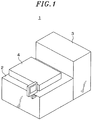
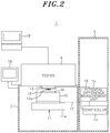
- FIGS. 1 and 2 are a schematic perspective view and a schematic front view, respectively, illustrating a configuration of a prober 1 as a test device including a stage as a substrate support according to the present embodiment.
- FIG. 2 illustrates certain components of an accommodation chamber and a loader of the prober 1 of FIG. 1 to be described below, and, thus, a cross section view thereof is presented.
- the stage 10 includes the top plate 120, the channel-forming member 130, and the light irradiation mechanism 140 in this order from the top.
- the stage 10 is supported by the moving mechanism 11, with the heat insulating member 110 interposed therebetween, from a lower portion of the light irradiation mechanism 140, in other words, from a rear surface of the light irradiation mechanism 140.
- Suction holes (not shown) for vacuum-attracting the wafer W are formed in the wafer supporting surface 120a of the top plate 120.
- a plurality of temperature sensors 121 are embedded in the top plate 120 at positions spaced apart from each other in a plan view.
- an average value of results detected by the temperature sensor 121 can be used.
- a temperature sensor may be provided to measure the temperature T cool and the temperature T LED-C , and when the temperature T cool and the temperature T LED-C are constant, the temperature T cool and the temperature T LED-C may be stored in advance in the storage unit (not shown) and read from the storage unit when the temperature T H is calculated.
- the stage 10 locally emits LED light onto the top plate 120 to heat the top plate 120 while cooling the entire top plate 120 with the refrigerant flowing in the refrigerant channel R, thereby cooling other electronic devices while controlling the temperature of a desired electronic device.
- the top plate 120 and the channel-forming member 130 are made of materials having different thermal expansion coefficients, and the stage 10 may be warped. Specifically, the top plate 120 may be warped.
- the transparent heater 150 is provided as a temperature adjustment part that is made of a material capable of transmitting light and controls the temperature of the channel-forming member. Therefore, according to the present embodiment, the temperature of the channel-forming member 130 is adjusted using the transparent heater 150, thereby preventing the top plate 120 from being warped.
- the operating conditions of the stage 10 used for calculating the temperature T H are not limited to such a combination and may be, for example, based only on the temperature T TP of the top plate 120 and the temperature T cool of the refrigerant flowing in the refrigerant channel R.
- the calculation of the temperature T H by the controller 14 may be performed using a function f (T TP , T cool ) based on the temperature T TP of the top plate 120 and the temperature T cool of the refrigerant flowing in the refrigerant channel R.
Landscapes
- Engineering & Computer Science (AREA)
- Physics & Mathematics (AREA)
- General Physics & Mathematics (AREA)
- Computer Hardware Design (AREA)
- Microelectronics & Electronic Packaging (AREA)
- General Engineering & Computer Science (AREA)
- Environmental & Geological Engineering (AREA)
- Health & Medical Sciences (AREA)
- Toxicology (AREA)
- Testing Or Measuring Of Semiconductors Or The Like (AREA)
- Container, Conveyance, Adherence, Positioning, Of Wafer (AREA)
Abstract
Description
- The present disclosure relates to a substrate support, a test device, and a method of adjusting a temperature of a substrate support.
- Japanese Patent Application Publication No.
2018-151369 Patent Document 1, the cooling unit and the refrigerant may transmit light, and a light irradiation mechanism including a plurality of light-emitting diodes (LEDs) is provided to face a wafer through the stage lid and the cooling unit. The cooling unit is made of glass, and the stage lid is made of silicon carbide (SiC). - The present disclosure is directed to a technique for suppressing warpage of a substrate support formed by bonding members made of materials having different thermal expansion coefficients.
- In accordance with an aspect of the present disclosure, there is provided a substrate support on which a substrate is placed. The substrate support comprises: a top plate portion having a surface on which a substrate is placed; a light irradiation mechanism which includes a plurality of light-emitting elements, is disposed to face the substrate placed on the top plate portion, and heats the substrate using light emitted from the light-emitting elements; a channel-forming member which transmits the light emitted from the light-emitting elements and is bonded to a rear surface of the top plate portion so as to be interposed between the top plate portion and the light irradiation mechanism. Further, refrigerant channels are formed between the channel-forming member and the top plate portion, a refrigerant which transmits the light emitted from the light-emitting elements flows through the refrigerant channels, and the top plate portion and the channel-forming member are made of materials having different thermal expansion coefficients; and a temperature adjustment part for adjusting a temperature of the channel-forming member by using light having a wavelength absorbed by a light-transmitting material or the channel-forming member.
- The objects and features of the present disclosure will become apparent from the following description of embodiments, given in conjunction with the accompanying drawings, in which:
-
FIG. 1 is a schematic perspective view illustrating a configuration of a prober as a test device including a stage that is a substrate support according to the present embodiment; -
FIG. 2 is a schematic front view showing the configuration of the prober as the test device including the stage that is the substrate support according to the present embodiment; -
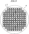
FIG. 3 is a schematic plan view representing a configuration of a wafer; -
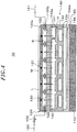
FIG. 4 is a schematic cross-sectional view describing a configuration of the stage; -
FIG. 5 is a schematic plan view depicting a configuration of a light irradiation mechanism; -
FIG. 6 is a schematic view explaining a configuration of a circuit for measuring the temperature of a wafer in the test device ofFIG. 1 ; and -
FIG. 7 is a view for describing an example of controlling a transparent heater. - In a semiconductor manufacturing process, a plurality of electronic devices having a predetermined circuit pattern are formed on a substrate such as a semiconductor wafer (hereinafter, referred to as "wafer"). The electronic devices so formed are tested with regard to electrical characteristics thereof and classified into a non-defective product or a defective product. The test of the electronic devices is performed using a test device, for example, while they are still on the substrate before division into individual electronic device.
- A test device referred to as a prober or the like (hereinafter, referred to as "prober") includes a probe card having a plurality of probes, and a substrate support on which a substrate is placed. At the time of a test, in the prober, each probe of the probe card comes in contact with each electrode of the electronic device, and in that state, a tester provided above the probe card supplies an electrical signal to the electronic device through each probe. It is determined whether the electronic device is a defective product based on the electrical signal received by the tester from the electronic device through each probe.
- When the electrical characteristics of the electronic device are tested by such type of prober, in order to simulate an environment in which the electronic device is mounted, a temperature of the substrate support and a temperature of the substrate are controlled by a heater having a resistance heating element or by a channel in which a refrigerant flows, provided on the substrate support.
- In recent years, as electronic devices have become faster and smaller, the degree of integration thereof has increased, and, thus, the amount of heat generated during operation has significantly increased. Therefore, during a test of an electronic device on a substrate, a heat load may be applied to other electronic devices adjacent thereto, which may cause a problem in the other electronic devices.
- In relation to the problem,
Patent Document 1 discloses the following stage, that is, a substrate support. The stage disclosed inPatent Document 1 includes a disk-shaped stage lid and a cooling unit having a refrigerant groove formed therein. The stage lid is in contact with the cooling unit through an O-ring, the refrigerant groove is covered with the stage lid to form a refrigerant channel, and the O-ring seals a refrigerant in the refrigerant channel. A light irradiation mechanism including a plurality of light-emitting diodes (LEDs) is provided to face a wafer through the stage lid and the cooling unit. In addition, the cooling unit and the refrigerant may transmit light so that light emitted from the LED passes through the cooling unit and the like and reaches the stage lid. Furthermore, the light irradiation mechanism may locally irradiate the stage lid with the light emitted from the LED. Due to such configuration, the stage disclosed inPatent Document 1 emits light locally onto the stage lid to only heat the stage lid while cooling the entire stage lid using the cooling unit, thereby cooling other electronic devices while controlling the temperature of a desired electronic device. - Conventionally, silicon carbide (SiC) having high thermal conductivity has been used as a material for a stage lid (that is, a material for a top plate portion of a stage) because light emitted from an LED can be easily used for heating, and glass, which is an inexpensive transparent member, has been used for a channel-forming member that forms a refrigerant channel together with the top plate portion. Specifically, glass, which is capable of transmitting light emitted from the LED and has a thermal expansion coefficient different from that of SiC used as a material for the top plate portion, has been conventionally used as the material for the channel-forming member.
- In some cases, in order to seal a refrigerant channel, a top plate portion and a channel-forming member may be bonded by using an epoxy resin or the like. In the case that the top plate portion and the channel-forming member are bonded by using the epoxy resin or the like, if the materials of the top plate portion and the channel-forming member have different thermal expansion coefficients as described above, a stage may be warped when a test is performed in a temperature zone significantly different from a temperature at the time of bonding. As such, if the stage is warped, for example, each probe of a probe card cannot be in uniform contact with a substrate on the stage, which may adversely affect test quality.
- Therefore, the technique according to the present disclosure suppresses warpage of a substrate support formed by way of bonding members made of materials having different thermal expansion coefficients.
- Hereinafter, a substrate support, a test device, and a method of adjusting warpage of the substrate support according to the present embodiment will be described with reference to the accompanying drawings. In the present specification and the drawings, elements having substantially the same function or structure are referred to by like reference numerals, and repeated descriptions thereof will be omitted.
-
FIGS. 1 and2 are a schematic perspective view and a schematic front view, respectively, illustrating a configuration of aprober 1 as a test device including a stage as a substrate support according to the present embodiment.FIG. 2 illustrates certain components of an accommodation chamber and a loader of theprober 1 ofFIG. 1 to be described below, and, thus, a cross section view thereof is presented. - The
prober 1 ofFIGS. 1 and2 tests the electrical characteristics of a wafer W, i.e., a substrate and a test target in the present embodiment. Specifically, theprober 1 tests the electrical characteristics of each of a plurality of electronic devices formed on the wafer W (see reference numeral D ofFIG. 3 described below). Theprober 1 includes anaccommodation chamber 2 for accommodating the wafer W at the time of a test, aloader 3 disposed adjacent to theaccommodation chamber 2, and atester 4 disposed to cover the accommodation chamber. - The
accommodation chamber 2 is a housing, the inside of which is hollow, and includes astage 10 on which the wafer W is mounted. - The
stage 10 vacuum-holds the wafer W such that a position of the wafer W is not misaligned with respect to thestage 10. In addition, thestage 10 is provided with amoving mechanism 11 for laterally and vertically moving thestage 10. The movingmechanism 11 includes abase 11a made of a metal material such as stainless steel, on which thestage 10 is disposed, and also includes a guide rail, a ball screw, and a motor for moving thebase 11a (not shown). Through themoving mechanism 11, the relative positions of aprobe card 12 to be described below and the wafer W may be adjusted so thatprobes 12a of theprobe card 12 may be brought into contact with electrodes on a surface of the wafer W. - The
probe card 12 including the plurality ofprobes 12a as contact terminals is disposed above thestage 10 so as to face thestage 10 in theaccommodation chamber 2. Theprobe card 12 is connected to thetester 4 through aninterface 13. Eachprobe 12a is in contact with an electrode of each electronic device of the wafer W at the time of testing electrical characteristics of the electronic device, supplies electric power from thetester 4 to the electronic device through theinterface 13, and transmits a signal from the electronic device to thetester 4 through theinterface 13. - The
loader 3 takes out the wafer W accommodated in a front opening unified pod (FOUP) (not shown), which is a transport container, and transfers the wafer W to thestage 10 of theaccommodation chamber 2. In addition, theloader 3 receives the wafer W from thestage 10 after the test of the electrical characteristics of the electronic devices thereon has been completed, and accommodates the wafer W in the FOUP. - Furthermore, the
loader 3 includes acontroller 14 that performs various types of control, such as control of a temperature of the electronic device to be tested. Thecontroller 14, also referred to as a base unit or the like, is composed of, for example, a computer provided with a central processing unit (CPU), a memory, and the like, and also includes a program storage unit (not shown). The program storage unit stores programs that control various processes in theprober 1. The program may be recorded on a computer-readable storage medium and may be installed in thecontroller 14 from the storage medium. Some or all of the programs may also be realized with dedicated hardware (circuit board). - In addition, the
loader 3 includes a potentialdifference measurement unit 15 for measuring a potential difference in a potential difference generation circuit (not shown) in the electronic device. The potential difference generation circuit is, for example, a diode, a transistor, or a resistor. The potentialdifference measurement unit 15 is connected to theinterface 13 through awire 16, acquires a potential difference between twoprobes 12a that are in contact with two electrodes corresponding to the potential difference generation circuit, and transmits the acquired potential difference to thecontroller 14. The connection structure of eachprobe 12a and thewire 16 in theinterface 13 will be described below. Thecontroller 14 is connected to thestage 10 through awire 17 and controls a flow rate control valve that adjusts the flow rate of a refrigerant in alight irradiation mechanism 140 to be described below or in refrigerant channels R described below. Thecontroller 14 or the potentialdifference measurement unit 15 may be provided in theaccommodation chamber 2, and the potentialdifference measurement unit 15 may be provided in theprobe card 12. - The
tester 4 includes a test board (not shown) that implements a certain portion of a circuit configuration of a motherboard on which an electronic device is mounted. The test board is connected to atester computer 18 that determines whether the electronic device is defective or non-defective based on a signal from the electronic device. In thetester 4, circuit configurations of a plurality of types of motherboards can be implemented by replacing the test board. - In addition, the
prober 1 includes auser interface unit 19 on which information is displayed for a user or through which the user inputs an instruction. Theuser interface unit 19 includes, for example, an input unit such as a touch panel or a keyboard, and a display unit such as a liquid crystal display. - In the
prober 1 including the above-described components, when the electrical characteristics of the electronic device are tested, thetester computer 18 transmits data to the test board connected to the electronic device through eachprobe 12a. Thetester computer 18 determines whether the transmitted data has been correctly processed by the test board based on an electrical signal from the test board. - Next, the wafer W to be tested by the
prober 1 will be described with reference toFIG. 3. FIG. 3 is a schematic plan view depicting a configuration of the wafer W. - As shown in
FIG. 3 , the plurality of electronic devices D have been formed on the surface of the wafer W at predetermined intervals by performing an etching process or an interconnection process on a substantially disk-shaped silicon substrate. Electrodes E are formed on a surface of the wafer W, i.e., on the electronic device D. The electrode E is electrically connected to a circuit element inside the electronic device D. By applying a voltage to the electrode E, a current may flow in the circuit element inside each electronic device D. The size of the electronic device D is, for example, 10 mm to 30 mm square in a plan view. - Next, the configuration of the
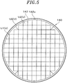
stage 10 will be described with reference toFIGS. 4 and5 .FIG. 4 is a schematic cross-sectional view representing the configuration of thestage 10, andFIG. 5 is a schematic plan view showing a configuration of thelight irradiation mechanism 140 to be described below. - As shown in
FIG. 4 , thestage 10 is formed by stacking a plurality of functional parts including atop plate 120 as a top plate portion. Thestage 10 is mounted on the moving mechanism 11 (seeFIG. 2 ) for laterally and vertically moving thestage 10 with aheat insulating member 110 interposed therebetween. Theheat insulating member 110 is for thermally insulating thestage 10 from the movingmechanism 11 and is made of, for example, a sintered body of cordierite having low thermal conductivity and a low thermal expansion coefficient. Both thebase 11a of the movingmechanism 11 and theheat insulating member 110 are solid bodies. - The
stage 10 includes thetop plate 120, the channel-formingmember 130, and thelight irradiation mechanism 140 in this order from the top. Thestage 10 is supported by the movingmechanism 11, with theheat insulating member 110 interposed therebetween, from a lower portion of thelight irradiation mechanism 140, in other words, from a rear surface of thelight irradiation mechanism 140. - The
top plate 120 is a member on which the wafer W is placed. To put it another way, thetop plate 120 is a member, asurface 120a of which is a wafer supporting surface serving as a substrate supporting surface on which the wafer W is placed. Hereinafter, in some cases, thesurface 120a of thetop plate 120, which is also an upper surface of thestage 10, will be referred to as thewafer supporting surface 120a. - The
top plate 120 is formed, for example, in a disk shape. In addition, thetop plate 120 is made of a material having low specific heat and high thermal conductivity, for example, silicon carbide (SiC). When thetop plate 120 is made of the above-described material, thetop plate 120 can be efficiently heated and cooled, and, thus, the wafer W placed on thetop plate 120 can be efficiently heated or cooled. Hereinafter, it is assumed that thetop plate 120 is made of SiC. - SiC has a high Young's modulus of 300 GPa. Therefore, by forming the
top plate 120 with SiC, it is possible to prevent thetop plate 120 from being cracked or the like - Suction holes (not shown) for vacuum-attracting the wafer W are formed in the
wafer supporting surface 120a of thetop plate 120. In addition, a plurality oftemperature sensors 121 are embedded in thetop plate 120 at positions spaced apart from each other in a plan view. - The channel-forming
member 130 is a member that is bonded to the rear surface of thetop plate 120 so as to be interposed between thetop plate 120 and thelight irradiation mechanism 140 and forms the refrigerant channels R in which the refrigerant flows between the light irradiation mechanism and thetop plate 120. The channel-formingmember 130 is formed in a disk shape having substantially the same diameter as thetop plate 120. - Meanwhile, grooves are formed in a
rear surface 120b of thetop plate 120 on which the channel-formingmember 130 is mounted, and the grooves are covered with the channel-formingmember 130 to form the refrigerant channels R. In theprober 1, thetop plate 120 is cooled by the refrigerant flowing in the refrigerant channels R, thereby cooling the wafer W placed on thetop plate 120, that is, on thestage 10, and specifically, thereby cooling the electronic devices formed on the wafer W. - In addition, a
supply port 122 and adischarge port 123 communicating with the refrigerant channel R are formed in thetop plate 120. Asupply pipe 160 for supplying the refrigerant to the refrigerant channel R is connected to thesupply port 122, and adischarge pipe 161 for discharging the refrigerant from the refrigerant channel R is connected to thedischarge port 123. Thesupply pipe 160 is provided with a flowrate control valve 162 that controls the flow rate of the refrigerant supplied to the refrigerant channel R. - A material capable of transmitting light (specifically, light emitted from
LEDs 141 described below), for example, a fluorine-based inert liquid (Fluorinert™ (registered trademark), Novec™ (registered trademark), or the like) is used as the refrigerant flowing in the refrigerant channel R, and the refrigerant is supplied to the refrigerant channel R through thesupply pipe 160 by a pump (not shown) provided outside theprober 1. The operation of the flowrate control valve 162 or the like for adjusting the flow rate of the refrigerant is controlled by thecontroller 14. - As a material of the channel-forming
member 130 constituting the refrigerant channel R as described above, a material capable of transmitting light (specifically, light emitted from theLED 141 described below) is used. In the following examples, it is assumed that the channel-formingmember 130 is made of glass. - In addition, the channel-forming
member 130 and thetop plate 120 are bonded such that the refrigerant is sealable in the refrigerant channel R. The bonding is performed using, for example, an epoxy resin. More specifically, an epoxy resin is applied between the channel-formingmember 130 and thetop plate 120, and the channel-formingmember 130 and thetop plate 120 are pressed against each other and heated to a predetermined temperature (for example, 100 °C.), thereby performing the bonding. - The
light irradiation mechanism 140 is disposed to face the wafer W placed on thewafer supporting surface 120a of thetop plate 120 with the channel-formingmember 130 interposed therebetween. - The
light irradiation mechanism 140 includes the plurality ofLEDs 141 as light-emitting elements facing the wafer W and heats the wafer W with light emitted from theLEDs 141. Specifically, thelight irradiation mechanism 140 includes a plurality of LED units U, each having a plurality ofLEDs 141 that are unitized, and also includes a base 142 on which the LED units U are mounted. For example, as shown inFIG. 5 , the LED units U in thelight irradiation mechanism 140 substantially cover the entire surface of the base 142 with the LED units U includes planar rectangular-shaped units U1 and planar nonrectangular-shaped units U2. The rectangular-shaped units U1 are arranged in the same manner as the electronic devices D (seeFIG. 3 ) formed on the wafer W, the number of the rectangular-shaped units U1 is the same as that of the electronic devices D, and the nonrectangular-shaped units U2 cover the outer circumference of the planar rectangular-shaped units U1. As a result, the light emitting from theLEDs 141 of the LED unit U may be emitted onto at least the entirely of a portion of thetop plate 120 in contact with the wafer W. - Each
LED 141 emits light toward the wafer W. In the present example, eachLED 141 emits near-infrared light. The light emitted from the LEDs 141 (hereinafter, in some cases, simply referred to as "LED light") passes through the channel-formingmember 130 of thestage 10, which is made of a light-transmitting member. The light passing through the channel-formingmember 130 passes through a refrigerant capable of transmitting light, which flows in the refrigerant channel R of thestage 10, and is incident on thetop plate 120. - In a plan view, the
base 142 is formed in a disk shape having substantially the same diameter as thetop plate 120. Furthermore, as shown inFIG. 4 , thebase 142 has aconcave portion 142a formed in a surface thereof, and theLEDs 141 are mounted in theconcave portion 142a. Theconcave portion 142a may be filled with a material capable of transmitting LED light. - In addition, the
base 142 has acooling water channel 142b, through which cooling water as a refrigerant for cooling theLEDs 141 flows, in a portion closer to a rear surface of the base 142 than theconcave portion 142a. Thebase 142 is made of a metal material such as aluminum (Al). - In addition, the
light irradiation mechanism 140 includes a drivingcircuit board 143 for driving theLEDs 141 and asupport member 144 on which thedriving circuit board 143 is mounted. - A
concave portion 144a is formed on a surface of thesupport member 144, and the drivingcircuit board 143 is mounted in theconcave portion 144a. Thesupport member 144 is made of a metal material such as Al. - In the
light irradiation mechanism 140, LED light, incident on thetop plate 120 on which the wafer W is placed, is controlled for each of the LED units U. Therefore, thelight irradiation mechanism 140 can emit the LED light only onto a certain portion on thetop plate 120 and can make the intensity of light irradiated onto a certain portion different from the intensity of light irradiated onto other portions. Therefore, thelight irradiation mechanism 140 can locally heat the wafer W placed on thetop plate 120 or may locally change how much the wafer W is to be heated. - In addition, the
stage 10 includes atransparent heater 150. Thetransparent heater 150 is an example of a temperature adjustment part that is made of a material capable of transmitting light and controls the temperature of the channel-formingmember 130. Thetransparent heater 150 is a resistance heating heater made of a conductive material capable of transmitting LED light (for example, light having a wavelength of 850 nm). Examples of the conductive material include indium tin oxide (ITO), indium zinc oxide (IZO), zinc oxide (ZnO), and IGZO (oxide semiconductor composed of indium (In), gallium (Ga), and zinc (Zn)). - The
transparent heater 150 is provided on the channel-formingmember 130, and specifically, thetransparent heater 150 is provided on a surface of the channel-formingmember 130 opposite to thetop plate 120, that is, on a rear surface of the channel-formingmember 130. In this case, thetransparent heater 150 is formed through, for example, a sputtering method or a deposition method. Formation of thetransparent heater 150 through the sputtering method or the like is performed in advance, for example, before thetop plate 120 and the channel-formingmember 130 are bonded. - The formation position of the
transparent heater 150 is not limited to the rear surface of the channel-formingmember 130 and may be inside the rear surface of the channel-formingmember 130. - In addition, a temperature sensor (not shown) for measuring a temperature of the channel-forming
member 130 is provided around thetransparent heater 150. - The
transparent heater 150 heats the channel-formingmember 130 so as to absorb a difference in thermal expansion coefficients of thetop plate 120 made of SiC and the channel-formingmember 130 made of glass having a thermal expansion coefficient different from that of SiC. In other words, thetransparent heater 150 heats the channel-formingmember 130 such that thestage 10 is not warped, and more specifically, thetransparent heater 150 heats the channel-formingmember 130 such that thetop plate 120 is not warped. - Heating of the channel-forming
member 130 by thetransparent heater 150, that is, a current passage amount in thetransparent heater 150, is controlled by thecontroller 14. - The
controller 14 controls thetransparent heater 150 such that the temperature of the channel-formingmember 130 measured by the above-described temperature sensor (not shown) provided around thetransparent heater 150 becomes the temperature TH of the channel-formingmember 130 at which thetop plate 120 is not warped. The temperature TH of the channel-formingmember 130 at which thetop plate 120 is not warped is calculated by thecontroller 14, for example, based on operating conditions of thestage 10. More specifically, the temperature TH of the channel-formingmember 130 at which thetop plate 120 is not warped is calculated by thecontroller 14 based on the temperature TTP of thetop plate 120, the temperature Tcool of a refrigerant flowing in the refrigerant channel R, and the temperature TLED-C of cooling water flowing in thecooling water channel 142b for cooling theLED 141. A relational expression between TH, TTP, Tcool, and TLED-C, that is, a function f (TTP, Tcool, TLED-C) used for the calculation is acquired in advance and stored in a storage unit (not shown).
- For the temperature TTP, for example, an average value of results detected by the
temperature sensor 121 can be used. A temperature sensor may be provided to measure the temperature Tcool and the temperature TLED-C, and when the temperature Tcool and the temperature TLED-C are constant, the temperature Tcool and the temperature TLED-C may be stored in advance in the storage unit (not shown) and read from the storage unit when the temperature TH is calculated. - In the
prober 1, the temperature of the electronic device D to be tested formed on the wafer W on thestage 10 is controlled to be constant at a target temperature through the heating by light emitted from thelight irradiation mechanism 140 and through the heat absorption by the refrigerant flowing in the refrigerant channel R. For the temperature control, theprober 1 measures the temperature of the electronic device D. -
FIG. 6 is a schematic diagram illustrating a configuration of a circuit for measuring the temperature of the electronic device D in theprober 1. - In the
prober 1, as shown inFIG. 6 , theprobes 12a are connected to thetester 4 through a plurality ofwires 20 disposed at theinterface 13. In addition, arelay 21 is provided in each of the twowires 20, among thewires 20, connecting thetester 4 and twoprobes 12a in contact with two electrodes E of the potential difference generation circuit (for example, a diode) in the electronic device D. - Each
relay 21 may be configured to switch between thetester 4 and the potentialdifference measurement unit 15 and transmit thereto the potential difference of each electrode E. For example, when the electrical characteristics of the electronic device D are tested, after the mounting voltage is applied on each electrode E, eachrelay 21 transmits the potential of each electrode E to the potentialdifference measurement unit 15 at a predetermined timing. In the above-described potential difference generation circuit, a potential difference generated by a current flow differs depending on a temperature. Therefore, the temperature of the electronic device D can be measured in real time during a test based on a potential difference of the potential difference generation circuit of the electronic device D, that is, a potential difference between the two electrodes E (probe 12a) of the potential difference generation circuit. In theprober 1, the potentialdifference measurement unit 15 acquires the potential difference of the potential difference generation circuit of the electronic device D based on the potential of each electrode E transmitted from eachrelay 21. In addition, the potentialdifference measurement unit 15 transmits the acquired potential difference to thecontroller 14. Thecontroller 14 measures the temperature of the electronic device D based on the transmitted potential difference and the temperature characteristics of the potential difference of the potential difference generation circuit. - A method of measuring the temperature of the electronic device D is not limited to the one described above, and other methods may be used as long as the temperature of the electronic device D may be measured.
- Next, an example of processing the wafer W using the
prober 1 will be described. - First, the wafer W is taken out of the FOUP of the
loader 3, transferred toward thestage 10, and placed on thewafer supporting surface 120a of thetop plate 120. Subsequently, thestage 10 is moved to a predetermined position. - All the
LEDs 141 of thelight irradiation mechanism 140 are turned on, and light output from theLEDs 141 and the flow rate of a refrigerant flowing in the refrigerant channel R are adjusted based on information acquired from thetemperature sensor 121 of thetop plate 120 such that the temperature of thetop plate 120 is made uniform at a surface thereof. - Then, the
stage 10 is moved, and eachprobe 12a provided above thestage 10 is brought into contact with the electrode E of the electronic device D to be tested of the wafer W. - In this state, the potential
difference measurement unit 15 acquires a potential difference of the above-described potential difference generation circuit in the electronic device D to be tested. The potential difference is calibrated such that the temperature of thetop plate 120 made uniform on the surface thereof substantially matches the temperature of the electronic device D to be tested, that is, information on temperature characteristics of the potential difference is corrected. - Thereafter, a signal for a test is input to each
probe 12a. As a result, a test of the electronic device D is started. Meanwhile, based on information on a potential difference generated in the potential difference generation circuit of the electronic device D to be tested during the test, for example, light output from theLEDs 141 of the LED unit U corresponding to the electronic device, that is, a voltage applied to theLEDs 141, is controlled such that the temperature of the electronic device D becomes a test temperature or a target temperature. In addition, the temperature and the flow rate of a refrigerant in the refrigerant channel R are constant at a value corresponding to the test temperature or the target temperature of the electronic device D to be tested. - Then, processes of correcting and testing the potential difference of the above-described potential difference generation circuit are repeatedly performed until the test of all electronic devices D is completed.
- In addition, the channel-forming
member 130 is heated by thetransparent heater 150 such that thetop plate 120 is not warped between the above-described processes of correcting and testing the potential difference of the potential difference generation circuit. For example, thecontroller 14 calculates the temperature TH of the channel-formingmember 130, at which thetop plate 120 is not warped, based on an average value of the temperatures TTP of thetop plate 120 measured by thetemperature sensor 121, the temperature Tcool of the refrigerant flowing in the refrigerant channel R, and the temperature TLED-C of the cooling water flowing in thecooling water channel 142b for cooling theLED 141. Thecontroller 14 controls thetransparent heater 150 such that the temperature of the channel-formingmember 130 measured by the temperature sensor (not shown) provided around thetransparent heater 150 becomes the temperature TH. - As such, the
top plate 120 is not warped during the above-described calibration and test of the potential difference of the potential difference generation circuit, and, thus, the wafer W vacuum-held by thetop plate 120 is in uniform contact with theprobes 12a of theprobe card 12. Therefore, the above-described calibration and test can be performed accurately. - The processing of the wafer W using the
prober 1 may include a process of photographing the surface of the wafer W on thetop plate 120 using an imaging device (not shown) provided in theaccommodation chamber 2. For example, in a process of aligning positions of theprobe 12a and the wafer W and a process of checking a mark of theprobe 12a, that is, a needle mark after the test, the electrode E on the wafer W is photographed by the imaging device. As described above, in the process of performing the photographing, theLEDs 141 may not be turned on. Even when theLEDs 141 are not turned on, thetop plate 120 may be warped. When thetop plate 120 is being warped during the photographing, the electrode of thetop plate 120 may not be in focus unless the height of the imaging device is changed. Thus, when thetop plate 120 is being warped, the process of aligning the positions or the process of checking the needle mark takes a long time. Therefore, even in these processes, thecontroller 14 may control thetransparent heater 150 such that the temperature of the channel-formingmember 130 measured by the temperature sensor (not shown) provided around thetransparent heater 150 becomes the temperature TH of the channel-formingmember 130 at which thetop plate 120 is not warped. As a result, it is possible to prevent the processes from taking a long time. - As described above, in the present embodiment, the
stage 10 includes thetop plate 120 having a surface on which the wafer W is placed, the channel-formingmember 130 capable of transmitting light, which is bonded to therear surface 120b of thetop plate 120 and forms the refrigerant channels R in which a refrigerant capable of transmitting light flows between the channel-formingmember 130 and thetop plate 120, and thelight irradiation mechanism 140 which includes the plurality ofLEDs 141, is disposed to face the wafer W placed on thetop plate 120 with the channel-formingmember 130 interposed therebetween, and heats the wafer W with light emitting from theLED 141. Therefore, thestage 10 locally emits LED light onto thetop plate 120 to heat thetop plate 120 while cooling the entiretop plate 120 with the refrigerant flowing in the refrigerant channel R, thereby cooling other electronic devices while controlling the temperature of a desired electronic device. In thestage 10, thetop plate 120 and the channel-formingmember 130 are made of materials having different thermal expansion coefficients, and thestage 10 may be warped. Specifically, thetop plate 120 may be warped. Thus, thetransparent heater 150 is provided as a temperature adjustment part that is made of a material capable of transmitting light and controls the temperature of the channel-forming member. Therefore, according to the present embodiment, the temperature of the channel-formingmember 130 is adjusted using thetransparent heater 150, thereby preventing thetop plate 120 from being warped. In addition, according to the present embodiment, since thetop plate 120 is not warped, the plurality ofprobes 12a can be in uniform contact with the electronic devices D, thereby accurately testing the electrical characteristics or the like using theprobe card 12 including the plurality ofprobes 12a. Furthermore, thestage 10 can be used in a wide test temperature range because thetop plate 120 is not warped regardless of a temperature of thetop plate 120, that is, regardless of a test temperature. - In the above-described example, the
controller 14 calculated the temperature TH of the channel-formingmember 130, at which thetop plate 120 is not warped, based on operating conditions of thestage 10 such as the temperature TTP of thetop plate 120, the temperature Tcool of the refrigerant flowing in the refrigerant channel R, and the temperature TLED-C of the cooling water flowing in thecooling water channel 142b for cooling theLEDs 141. Specifically, thecontroller 14 calculated and acquired the temperature TH based on the function f (TTP, Tcool, TLED-C) . The operating conditions of thestage 10 used for calculating the temperature TH are not limited to such a combination and may be, for example, based only on the temperature TTP of thetop plate 120 and the temperature Tcool of the refrigerant flowing in the refrigerant channel R. In other words, the calculation of the temperature TH by thecontroller 14 may be performed using a function f (TTP, Tcool) based on the temperature TTP of thetop plate 120 and the temperature Tcool of the refrigerant flowing in the refrigerant channel R. - In addition, in the above-described example, the temperature TH of the channel-forming
member 130 at which thetop plate 120 is not warped has been calculated and acquired based on the operating conditions of thestage 10. A method for acquiring the temperature TH is not limited thereto, and for example, the temperature TH may be acquired as follows. That is, the temperature TH of the channel-formingmember 130, at which thetop plate 120 is not warped, is determined in advance for each operating condition of thestage 10 and is stored in the storage unit (not shown). At the time of a test, thecontroller 14 may acquire the temperature TH by reading the temperature TH, which meets an operating condition of thestage 10 at the time of the test, from the storage unit. More specifically, for example, different temperatures TH for a case where theLEDs 141 are turned on and a case where theLEDs 141 are turned off may be determined in advance and stored in the storage unit, and thecontroller 14 may select the temperature TH to be read from the storage unit according to whether theLEDs 141 are turned on or off. Even through such a method, it is possible to prevent thetop plate 120 from being warped regardless of a predicted amount of the warpage of thetop plate 120. -
FIG. 7 is a view for describing an example of controlling thetransparent heater 150. - As shown in
FIG. 7 , the channel-formingmember 130 may be divided into a plurality of regions A (five in the present example), and thecontroller 14 may control a heating amount of the channel-formingmember 130 by thetransparent heater 150 for each region A. Specifically, for example, a temperature sensor (not shown) is provided around thetransparent heater 150 for each region A of the channel-formingmember 130. Thecontroller 14 calculates the temperature TH of the channel-formingmember 130, at which thetop plate 120 is not warped, from the above-described function f (TTP, Tcool, TLED-C) based on the temperature TTP of thetop plate 120, which corresponds to the corresponding region A, measured by thetemperature sensor 121, the temperature Tcool of the refrigerant, and the temperature TLED-C of the cooling water. In addition, thecontroller 14 controls thetransparent heater 150 such that the temperature of each area A measured by the above-described temperature sensor (not shown) provided for each area A of the channel-formingmember 130 becomes the temperature TH calculated for each region A. - Therefore, it possible to prevent the
top plate 120 from being partially strongly heated to partially warp thetop plate 120. - In the above-described example, the
transparent heater 150 is used as a temperature adjustment part for controlling the temperature of the channel-formingmember 130, but the temperature adjustment part is not limited thereto. For example, the temperature adjustment part may include a light source emitting light with a wavelength different from that from theLEDs 141, specifically, a light source emitting light with a wavelength absorbed by the channel-formingmember 130, thereby heating the channel-formingmember 130 with the light to adjust a temperature. In addition, when the temperature adjustment part is for cooling the channel-formingmember 130, the rear surface of the channel-formingmember 130 may be cooled by a gas capable of transmitting light (carbon dioxide (CO2) gas, or the like). In this case, a cooling gas such as a carbon dioxide (CO2) gas is supplied to theconcave portion 142a of thebase 142. Therefore, theLEDs 141 can also be cooled by the cooling gas, thereby extending the lifetime of theLEDs 141. - For example, in the above-described example, a refrigerant groove is formed on a rear surface of a top plate, and the refrigerant groove is covered with a channel-forming member to form a refrigerant channel. Instead of this, a refrigerant groove may be formed in a surface of a channel-forming member, and the refrigerant groove may be covered with a flat plate-shaped top plate to form a refrigerant channel.
- When the warpage of the wafer W can adversely affect a processing result, the substrate support according to the present disclosure may be provided in a device other than a test device such as a prober, for example, a film forming device, an etching device, a doping device, or the like.
- The presently disclosed embodiments are considered in all respects to be illustrative and not restrictive. The above-described embodiments can be embodied in various forms. Further, the above-described embodiments may be omitted, replaced, or changed in various forms without departing from the scope of the appended claims and the gist thereof.
Claims (7)
- A substrate support on which a substrate is placed, the substrate support comprising:a top plate portion having a surface on which a substrate is placed;a light irradiation mechanism that includes a plurality of light-emitting elements, is disposed to face the substrate placed on the top plate portion, and heats the substrate using light emitted from the light-emitting elements;a channel-forming member that transmits the light emitted from the light-emitting elements and is bonded to a rear surface of the top plate portion so as to be interposed between the top plate portion and the light irradiation mechanism, wherein refrigerant channels are formed between the channel-forming member and the top plate portion, a refrigerant, which transmits the light emitted from the light-emitting elements, flows through the refrigerant channels, and the top plate portion and the channel-forming member are made of materials having different thermal expansion coefficients; anda temperature adjustment part configured to adjust a temperature of the channel-forming member by using light having a wavelength absorbed by a light-transmitting material or the channel-forming member.
- The substrate support of claim 1, further comprising:a cooling unit configured to cool a driving unit for driving the light-emitting elements using a refrigerant; anda controller configured to control the temperature adjustment part,wherein the controller controls the temperature adjustment part such that the channel-forming member is at a temperature at which the top plate portion is not warped, and said temperature is calculated based on a temperature of the top plate portion, a temperature of the refrigerant of the refrigerant channel, and a temperature of the refrigerant of the cooling unit.
- The substrate support of claim 1, further comprising a controller configured to control the temperature adjustment part,
wherein the controller controls the temperature adjustment part such that the channel-forming member is at a temperature at which the top plate portion is not warped, and said temperature is predetermined for each operating condition of the substrate support. - The substrate support of any one of claims 1 to 3, wherein the temperature adjustment part is a resistance heating heater made of a light-transmitting material and is provided on a surface of the channel-forming member opposite to the top plate portion or inside the channel-forming member.
- The substrate support of claim 4, wherein the resistance heating heater is made of indium tin oxide (ITO), indium zinc oxide (IZO), zinc oxide (ZnO), or indium gallium zinc oxide (IGZO) .
- A test device comprising the substrate support of any one of claims 1 to 5, configured to test electrical characteristics of the substrate placed on the top plate portion by making a plurality of contact terminals be in contact with the substrate.
- A method of suppressing warpage of a substrate support on which a substrate is placed,
the substrate support including:a top plate portion having a surface on which a substrate is placed;a light irradiation mechanism that includes a plurality of light-emitting elements, is disposed to face the substrate placed on the top plate portion, and heats the substrate using light emitted from the light-emitting elements; anda channel-forming member that transmits the light emitted from the light-emitting elements and is bonded to a rear surface of the top plate portion so as to be interposed between the top plate portion and the light irradiation mechanism, wherein refrigerant channels are formed between the channel-forming member and the top plate portion, a refrigerant, which transmits the light emitted from the light-emitting elements, flows through the refrigerant channels, and the top plate portion and the channel-forming member are made of materials having different thermal expansion coefficients,the method comprising: adjusting a temperature of the channel-forming member by using light having a wavelength absorbed by a light-transmitting material or the channel-forming member.
Applications Claiming Priority (1)
| Application Number | Priority Date | Filing Date | Title |
|---|---|---|---|
| JP2020046016A JP7393986B2 (en) | 2020-03-17 | 2020-03-17 | Mounting table and inspection equipment |
Publications (2)
| Publication Number | Publication Date |
|---|---|
| EP3882644A1 true EP3882644A1 (en) | 2021-09-22 |
| EP3882644B1 EP3882644B1 (en) | 2024-04-17 |
Family
ID=74871219
Family Applications (1)
| Application Number | Title | Priority Date | Filing Date |
|---|---|---|---|
| EP21161985.3A Active EP3882644B1 (en) | 2020-03-17 | 2021-03-11 | Substrate support, test device, and method of adjusting temperature of substrate support |
Country Status (6)
| Country | Link |
|---|---|
| US (1) | US11810800B2 (en) |
| EP (1) | EP3882644B1 (en) |
| JP (1) | JP7393986B2 (en) |
| KR (1) | KR102524161B1 (en) |
| CN (1) | CN113406471B (en) |
| TW (1) | TWI860459B (en) |
Families Citing this family (1)
| Publication number | Priority date | Publication date | Assignee | Title |
|---|---|---|---|---|
| JP2025520231A (en) * | 2022-06-29 | 2025-07-03 | 沈陽芯源微電子設備股▲ふん▼有限公司 | Semiconductor substrate heating device, semiconductor device and temperature control method |
Citations (4)
| Publication number | Priority date | Publication date | Assignee | Title |
|---|---|---|---|---|
| US20050270056A1 (en) * | 2004-06-07 | 2005-12-08 | Scott Rumbaugh | Thermal optical chuck |
| US20160379853A1 (en) * | 2015-06-29 | 2016-12-29 | Varian Semiconductor Equipment Associates, Inc. | Electrostatic Chuck With LED Heating |
| JP2018151369A (en) | 2016-11-29 | 2018-09-27 | 東京エレクトロン株式会社 | Placing stand and electronic device inspection apparatus |
| JP2019106491A (en) * | 2017-12-13 | 2019-06-27 | 東京エレクトロン株式会社 | Inspection device |
Family Cites Families (11)
| Publication number | Priority date | Publication date | Assignee | Title |
|---|---|---|---|---|
| JP2006329816A (en) * | 2005-05-26 | 2006-12-07 | Sanyo Electric Co Ltd | Probe inspection device |
| JP4605387B2 (en) * | 2005-12-12 | 2011-01-05 | 住友電気工業株式会社 | Temperature characteristic inspection device |
| JP5071131B2 (en) * | 2008-01-31 | 2012-11-14 | 東京エレクトロン株式会社 | Probe device |
| JP2010186765A (en) | 2009-02-10 | 2010-08-26 | Sumitomo Electric Ind Ltd | Wafer supporter for wafer prober and wafer prober carrying the same |
| US8939606B2 (en) | 2010-02-26 | 2015-01-27 | Guardian Industries Corp. | Heatable lens for luminaires, and/or methods of making the same |
| JP2017133948A (en) * | 2016-01-28 | 2017-08-03 | セイコーエプソン株式会社 | Electronic component conveying device and electronic component inspection device |
| JP6655996B2 (en) * | 2016-01-19 | 2020-03-04 | 東京エレクトロン株式会社 | Substrate temperature control device and substrate processing device |
| CN109983350B (en) * | 2016-11-29 | 2022-02-22 | 东京毅力科创株式会社 | Stages and test equipment for electronic devices |
| JP6616363B2 (en) | 2017-09-05 | 2019-12-04 | 日本特殊陶業株式会社 | Holding device |
| JP7078838B2 (en) * | 2017-12-01 | 2022-06-01 | 東京エレクトロン株式会社 | Prober |
| JP7161854B2 (en) * | 2018-03-05 | 2022-10-27 | 東京エレクトロン株式会社 | inspection equipment |
-
2020
- 2020-03-17 JP JP2020046016A patent/JP7393986B2/en active Active
-
2021
- 2021-03-05 KR KR1020210029366A patent/KR102524161B1/en active Active
- 2021-03-08 TW TW110108095A patent/TWI860459B/en active
- 2021-03-10 CN CN202110261917.7A patent/CN113406471B/en active Active
- 2021-03-11 EP EP21161985.3A patent/EP3882644B1/en active Active
- 2021-03-11 US US17/198,704 patent/US11810800B2/en active Active
Patent Citations (5)
| Publication number | Priority date | Publication date | Assignee | Title |
|---|---|---|---|---|
| US20050270056A1 (en) * | 2004-06-07 | 2005-12-08 | Scott Rumbaugh | Thermal optical chuck |
| US20160379853A1 (en) * | 2015-06-29 | 2016-12-29 | Varian Semiconductor Equipment Associates, Inc. | Electrostatic Chuck With LED Heating |
| JP2018151369A (en) | 2016-11-29 | 2018-09-27 | 東京エレクトロン株式会社 | Placing stand and electronic device inspection apparatus |
| JP2019106491A (en) * | 2017-12-13 | 2019-06-27 | 東京エレクトロン株式会社 | Inspection device |
| US20200386805A1 (en) * | 2017-12-13 | 2020-12-10 | Tokyo Electron Limited | Inspection device |
Also Published As
| Publication number | Publication date |
|---|---|
| TWI860459B (en) | 2024-11-01 |
| JP7393986B2 (en) | 2023-12-07 |
| US11810800B2 (en) | 2023-11-07 |
| CN113406471A (en) | 2021-09-17 |
| KR102524161B1 (en) | 2023-04-20 |
| CN113406471B (en) | 2024-07-12 |
| JP2021150354A (en) | 2021-09-27 |
| KR20210116265A (en) | 2021-09-27 |
| US20210296145A1 (en) | 2021-09-23 |
| EP3882644B1 (en) | 2024-04-17 |
| TW202203339A (en) | 2022-01-16 |
Similar Documents
| Publication | Publication Date | Title |
|---|---|---|
| EP3799111B1 (en) | Inspection device and temperature control method | |
| EP3550313B1 (en) | Electronic device inspecting apparatus | |
| CN111788666B (en) | Check device | |
| CN109983350B (en) | Stages and test equipment for electronic devices | |
| US11796400B2 (en) | Lifetime estimating system and method for heating source, and inspection apparatus | |
| US11221358B2 (en) | Placement stand and electronic device inspecting apparatus | |
| US11828794B2 (en) | Placement table, testing device, and testing method | |
| US11810800B2 (en) | Substrate support, test device, and method of adjusting temperature of substrate support | |
| US11557494B2 (en) | Substrate support and inspection apparatus | |
| KR102660269B1 (en) | Heating device and led control method | |
| JP7449814B2 (en) | Inspection method and inspection device |
Legal Events
| Date | Code | Title | Description |
|---|---|---|---|
| PUAI | Public reference made under article 153(3) epc to a published international application that has entered the european phase |
Free format text: ORIGINAL CODE: 0009012 |
|
| STAA | Information on the status of an ep patent application or granted ep patent |
Free format text: STATUS: REQUEST FOR EXAMINATION WAS MADE |
|
| 17P | Request for examination filed |
Effective date: 20210311 |
|
| AK | Designated contracting states |
Kind code of ref document: A1 Designated state(s): AL AT BE BG CH CY CZ DE DK EE ES FI FR GB GR HR HU IE IS IT LI LT LU LV MC MK MT NL NO PL PT RO RS SE SI SK SM TR |
|
| GRAP | Despatch of communication of intention to grant a patent |
Free format text: ORIGINAL CODE: EPIDOSNIGR1 |
|
| STAA | Information on the status of an ep patent application or granted ep patent |
Free format text: STATUS: GRANT OF PATENT IS INTENDED |
|
| RIC1 | Information provided on ipc code assigned before grant |
Ipc: G01R 31/28 20060101AFI20231024BHEP |
|
| INTG | Intention to grant announced |
Effective date: 20231110 |
|
| RIN1 | Information on inventor provided before grant (corrected) |
Inventor name: NAKAYAMA, HIROYUKI |
|
| GRAS | Grant fee paid |
Free format text: ORIGINAL CODE: EPIDOSNIGR3 |
|
| GRAA | (expected) grant |
Free format text: ORIGINAL CODE: 0009210 |
|
| STAA | Information on the status of an ep patent application or granted ep patent |
Free format text: STATUS: THE PATENT HAS BEEN GRANTED |
|
| AK | Designated contracting states |
Kind code of ref document: B1 Designated state(s): AL AT BE BG CH CY CZ DE DK EE ES FI FR GB GR HR HU IE IS IT LI LT LU LV MC MK MT NL NO PL PT RO RS SE SI SK SM TR |
|
| REG | Reference to a national code |
Ref country code: GB Ref legal event code: FG4D |
|
| REG | Reference to a national code |
Ref country code: CH Ref legal event code: EP |
|
| REG | Reference to a national code |
Ref country code: IE Ref legal event code: FG4D Ref country code: DE Ref legal event code: R096 Ref document number: 602021011779 Country of ref document: DE |
|
| REG | Reference to a national code |
Ref country code: LT Ref legal event code: MG9D |
|
| REG | Reference to a national code |
Ref country code: NL Ref legal event code: MP Effective date: 20240417 |
|
| REG | Reference to a national code |
Ref country code: AT Ref legal event code: MK05 Ref document number: 1677739 Country of ref document: AT Kind code of ref document: T Effective date: 20240417 |
|
| PG25 | Lapsed in a contracting state [announced via postgrant information from national office to epo] |
Ref country code: NL Free format text: LAPSE BECAUSE OF FAILURE TO SUBMIT A TRANSLATION OF THE DESCRIPTION OR TO PAY THE FEE WITHIN THE PRESCRIBED TIME-LIMIT Effective date: 20240417 |
|
| PG25 | Lapsed in a contracting state [announced via postgrant information from national office to epo] |
Ref country code: NL Free format text: LAPSE BECAUSE OF FAILURE TO SUBMIT A TRANSLATION OF THE DESCRIPTION OR TO PAY THE FEE WITHIN THE PRESCRIBED TIME-LIMIT Effective date: 20240417 |
|
| PG25 | Lapsed in a contracting state [announced via postgrant information from national office to epo] |
Ref country code: IS Free format text: LAPSE BECAUSE OF FAILURE TO SUBMIT A TRANSLATION OF THE DESCRIPTION OR TO PAY THE FEE WITHIN THE PRESCRIBED TIME-LIMIT Effective date: 20240817 |
|
| PG25 | Lapsed in a contracting state [announced via postgrant information from national office to epo] |
Ref country code: BG Free format text: LAPSE BECAUSE OF FAILURE TO SUBMIT A TRANSLATION OF THE DESCRIPTION OR TO PAY THE FEE WITHIN THE PRESCRIBED TIME-LIMIT Effective date: 20240417 |
|
| PG25 | Lapsed in a contracting state [announced via postgrant information from national office to epo] |
Ref country code: HR Free format text: LAPSE BECAUSE OF FAILURE TO SUBMIT A TRANSLATION OF THE DESCRIPTION OR TO PAY THE FEE WITHIN THE PRESCRIBED TIME-LIMIT Effective date: 20240417 Ref country code: FI Free format text: LAPSE BECAUSE OF FAILURE TO SUBMIT A TRANSLATION OF THE DESCRIPTION OR TO PAY THE FEE WITHIN THE PRESCRIBED TIME-LIMIT Effective date: 20240417 |
|
| PG25 | Lapsed in a contracting state [announced via postgrant information from national office to epo] |
Ref country code: GR Free format text: LAPSE BECAUSE OF FAILURE TO SUBMIT A TRANSLATION OF THE DESCRIPTION OR TO PAY THE FEE WITHIN THE PRESCRIBED TIME-LIMIT Effective date: 20240718 |
|
| PG25 | Lapsed in a contracting state [announced via postgrant information from national office to epo] |
Ref country code: PT Free format text: LAPSE BECAUSE OF FAILURE TO SUBMIT A TRANSLATION OF THE DESCRIPTION OR TO PAY THE FEE WITHIN THE PRESCRIBED TIME-LIMIT Effective date: 20240819 |
|
| PG25 | Lapsed in a contracting state [announced via postgrant information from national office to epo] |
Ref country code: ES Free format text: LAPSE BECAUSE OF FAILURE TO SUBMIT A TRANSLATION OF THE DESCRIPTION OR TO PAY THE FEE WITHIN THE PRESCRIBED TIME-LIMIT Effective date: 20240417 |
|
| PG25 | Lapsed in a contracting state [announced via postgrant information from national office to epo] |
Ref country code: AT Free format text: LAPSE BECAUSE OF FAILURE TO SUBMIT A TRANSLATION OF THE DESCRIPTION OR TO PAY THE FEE WITHIN THE PRESCRIBED TIME-LIMIT Effective date: 20240417 |
|
| PG25 | Lapsed in a contracting state [announced via postgrant information from national office to epo] |
Ref country code: PL Free format text: LAPSE BECAUSE OF FAILURE TO SUBMIT A TRANSLATION OF THE DESCRIPTION OR TO PAY THE FEE WITHIN THE PRESCRIBED TIME-LIMIT Effective date: 20240417 |
|
| PG25 | Lapsed in a contracting state [announced via postgrant information from national office to epo] |
Ref country code: LV Free format text: LAPSE BECAUSE OF FAILURE TO SUBMIT A TRANSLATION OF THE DESCRIPTION OR TO PAY THE FEE WITHIN THE PRESCRIBED TIME-LIMIT Effective date: 20240417 |
|
| PG25 | Lapsed in a contracting state [announced via postgrant information from national office to epo] |
Ref country code: PT Free format text: LAPSE BECAUSE OF FAILURE TO SUBMIT A TRANSLATION OF THE DESCRIPTION OR TO PAY THE FEE WITHIN THE PRESCRIBED TIME-LIMIT Effective date: 20240819 Ref country code: PL Free format text: LAPSE BECAUSE OF FAILURE TO SUBMIT A TRANSLATION OF THE DESCRIPTION OR TO PAY THE FEE WITHIN THE PRESCRIBED TIME-LIMIT Effective date: 20240417 Ref country code: NO Free format text: LAPSE BECAUSE OF FAILURE TO SUBMIT A TRANSLATION OF THE DESCRIPTION OR TO PAY THE FEE WITHIN THE PRESCRIBED TIME-LIMIT Effective date: 20240717 Ref country code: LV Free format text: LAPSE BECAUSE OF FAILURE TO SUBMIT A TRANSLATION OF THE DESCRIPTION OR TO PAY THE FEE WITHIN THE PRESCRIBED TIME-LIMIT Effective date: 20240417 Ref country code: IS Free format text: LAPSE BECAUSE OF FAILURE TO SUBMIT A TRANSLATION OF THE DESCRIPTION OR TO PAY THE FEE WITHIN THE PRESCRIBED TIME-LIMIT Effective date: 20240817 Ref country code: HR Free format text: LAPSE BECAUSE OF FAILURE TO SUBMIT A TRANSLATION OF THE DESCRIPTION OR TO PAY THE FEE WITHIN THE PRESCRIBED TIME-LIMIT Effective date: 20240417 Ref country code: GR Free format text: LAPSE BECAUSE OF FAILURE TO SUBMIT A TRANSLATION OF THE DESCRIPTION OR TO PAY THE FEE WITHIN THE PRESCRIBED TIME-LIMIT Effective date: 20240718 Ref country code: FI Free format text: LAPSE BECAUSE OF FAILURE TO SUBMIT A TRANSLATION OF THE DESCRIPTION OR TO PAY THE FEE WITHIN THE PRESCRIBED TIME-LIMIT Effective date: 20240417 Ref country code: ES Free format text: LAPSE BECAUSE OF FAILURE TO SUBMIT A TRANSLATION OF THE DESCRIPTION OR TO PAY THE FEE WITHIN THE PRESCRIBED TIME-LIMIT Effective date: 20240417 Ref country code: BG Free format text: LAPSE BECAUSE OF FAILURE TO SUBMIT A TRANSLATION OF THE DESCRIPTION OR TO PAY THE FEE WITHIN THE PRESCRIBED TIME-LIMIT Effective date: 20240417 Ref country code: AT Free format text: LAPSE BECAUSE OF FAILURE TO SUBMIT A TRANSLATION OF THE DESCRIPTION OR TO PAY THE FEE WITHIN THE PRESCRIBED TIME-LIMIT Effective date: 20240417 Ref country code: RS Free format text: LAPSE BECAUSE OF FAILURE TO SUBMIT A TRANSLATION OF THE DESCRIPTION OR TO PAY THE FEE WITHIN THE PRESCRIBED TIME-LIMIT Effective date: 20240717 |
|
| PG25 | Lapsed in a contracting state [announced via postgrant information from national office to epo] |
Ref country code: DK Free format text: LAPSE BECAUSE OF FAILURE TO SUBMIT A TRANSLATION OF THE DESCRIPTION OR TO PAY THE FEE WITHIN THE PRESCRIBED TIME-LIMIT Effective date: 20240417 |
|
| REG | Reference to a national code |
Ref country code: DE Ref legal event code: R097 Ref document number: 602021011779 Country of ref document: DE |
|
| PG25 | Lapsed in a contracting state [announced via postgrant information from national office to epo] |
Ref country code: EE Free format text: LAPSE BECAUSE OF FAILURE TO SUBMIT A TRANSLATION OF THE DESCRIPTION OR TO PAY THE FEE WITHIN THE PRESCRIBED TIME-LIMIT Effective date: 20240417 |
|
| PG25 | Lapsed in a contracting state [announced via postgrant information from national office to epo] |
Ref country code: CZ Free format text: LAPSE BECAUSE OF FAILURE TO SUBMIT A TRANSLATION OF THE DESCRIPTION OR TO PAY THE FEE WITHIN THE PRESCRIBED TIME-LIMIT Effective date: 20240417 |
|
| PG25 | Lapsed in a contracting state [announced via postgrant information from national office to epo] |
Ref country code: RO Free format text: LAPSE BECAUSE OF FAILURE TO SUBMIT A TRANSLATION OF THE DESCRIPTION OR TO PAY THE FEE WITHIN THE PRESCRIBED TIME-LIMIT Effective date: 20240417 Ref country code: SK Free format text: LAPSE BECAUSE OF FAILURE TO SUBMIT A TRANSLATION OF THE DESCRIPTION OR TO PAY THE FEE WITHIN THE PRESCRIBED TIME-LIMIT Effective date: 20240417 |
|
| PG25 | Lapsed in a contracting state [announced via postgrant information from national office to epo] |
Ref country code: SM Free format text: LAPSE BECAUSE OF FAILURE TO SUBMIT A TRANSLATION OF THE DESCRIPTION OR TO PAY THE FEE WITHIN THE PRESCRIBED TIME-LIMIT Effective date: 20240417 |
|
| PG25 | Lapsed in a contracting state [announced via postgrant information from national office to epo] |
Ref country code: SM Free format text: LAPSE BECAUSE OF FAILURE TO SUBMIT A TRANSLATION OF THE DESCRIPTION OR TO PAY THE FEE WITHIN THE PRESCRIBED TIME-LIMIT Effective date: 20240417 Ref country code: SK Free format text: LAPSE BECAUSE OF FAILURE TO SUBMIT A TRANSLATION OF THE DESCRIPTION OR TO PAY THE FEE WITHIN THE PRESCRIBED TIME-LIMIT Effective date: 20240417 Ref country code: RO Free format text: LAPSE BECAUSE OF FAILURE TO SUBMIT A TRANSLATION OF THE DESCRIPTION OR TO PAY THE FEE WITHIN THE PRESCRIBED TIME-LIMIT Effective date: 20240417 Ref country code: EE Free format text: LAPSE BECAUSE OF FAILURE TO SUBMIT A TRANSLATION OF THE DESCRIPTION OR TO PAY THE FEE WITHIN THE PRESCRIBED TIME-LIMIT Effective date: 20240417 Ref country code: DK Free format text: LAPSE BECAUSE OF FAILURE TO SUBMIT A TRANSLATION OF THE DESCRIPTION OR TO PAY THE FEE WITHIN THE PRESCRIBED TIME-LIMIT Effective date: 20240417 Ref country code: CZ Free format text: LAPSE BECAUSE OF FAILURE TO SUBMIT A TRANSLATION OF THE DESCRIPTION OR TO PAY THE FEE WITHIN THE PRESCRIBED TIME-LIMIT Effective date: 20240417 |
|
| PG25 | Lapsed in a contracting state [announced via postgrant information from national office to epo] |
Ref country code: IT Free format text: LAPSE BECAUSE OF FAILURE TO SUBMIT A TRANSLATION OF THE DESCRIPTION OR TO PAY THE FEE WITHIN THE PRESCRIBED TIME-LIMIT Effective date: 20240417 |
|
| PLBE | No opposition filed within time limit |
Free format text: ORIGINAL CODE: 0009261 |
|
| STAA | Information on the status of an ep patent application or granted ep patent |
Free format text: STATUS: NO OPPOSITION FILED WITHIN TIME LIMIT |
|
| 26N | No opposition filed |
Effective date: 20250120 |
|
| PG25 | Lapsed in a contracting state [announced via postgrant information from national office to epo] |
Ref country code: SI Free format text: LAPSE BECAUSE OF FAILURE TO SUBMIT A TRANSLATION OF THE DESCRIPTION OR TO PAY THE FEE WITHIN THE PRESCRIBED TIME-LIMIT Effective date: 20240417 |
|
| PG25 | Lapsed in a contracting state [announced via postgrant information from national office to epo] |
Ref country code: SE Free format text: LAPSE BECAUSE OF FAILURE TO SUBMIT A TRANSLATION OF THE DESCRIPTION OR TO PAY THE FEE WITHIN THE PRESCRIBED TIME-LIMIT Effective date: 20240417 |
|
| PG25 | Lapsed in a contracting state [announced via postgrant information from national office to epo] |
Ref country code: MC Free format text: LAPSE BECAUSE OF FAILURE TO SUBMIT A TRANSLATION OF THE DESCRIPTION OR TO PAY THE FEE WITHIN THE PRESCRIBED TIME-LIMIT Effective date: 20240417 |
|
| REG | Reference to a national code |
Ref country code: CH Ref legal event code: H13 Free format text: ST27 STATUS EVENT CODE: U-0-0-H10-H13 (AS PROVIDED BY THE NATIONAL OFFICE) Effective date: 20251023 |
|
| PG25 | Lapsed in a contracting state [announced via postgrant information from national office to epo] |
Ref country code: LU Free format text: LAPSE BECAUSE OF NON-PAYMENT OF DUE FEES Effective date: 20250311 |
|
| GBPC | Gb: european patent ceased through non-payment of renewal fee |
Effective date: 20250311 |
|
| REG | Reference to a national code |
Ref country code: BE Ref legal event code: MM Effective date: 20250331 |
|
| PG25 | Lapsed in a contracting state [announced via postgrant information from national office to epo] |
Ref country code: GB Free format text: LAPSE BECAUSE OF NON-PAYMENT OF DUE FEES Effective date: 20250311 |
|
| PG25 | Lapsed in a contracting state [announced via postgrant information from national office to epo] |
Ref country code: FR Free format text: LAPSE BECAUSE OF NON-PAYMENT OF DUE FEES Effective date: 20250331 |
|
| PG25 | Lapsed in a contracting state [announced via postgrant information from national office to epo] |
Ref country code: BE Free format text: LAPSE BECAUSE OF NON-PAYMENT OF DUE FEES Effective date: 20250331 |
|
| PG25 | Lapsed in a contracting state [announced via postgrant information from national office to epo] |
Ref country code: CH Free format text: LAPSE BECAUSE OF NON-PAYMENT OF DUE FEES Effective date: 20250331 |
|
| PG25 | Lapsed in a contracting state [announced via postgrant information from national office to epo] |
Ref country code: IE Free format text: LAPSE BECAUSE OF NON-PAYMENT OF DUE FEES Effective date: 20250311 |
|
| PGFP | Annual fee paid to national office [announced via postgrant information from national office to epo] |
Ref country code: DE Payment date: 20260128 Year of fee payment: 6 |