EP3881365B1 - Memory device and method for its operation - Google Patents
Memory device and method for its operation Download PDFInfo
- Publication number
- EP3881365B1 EP3881365B1 EP19805621.0A EP19805621A EP3881365B1 EP 3881365 B1 EP3881365 B1 EP 3881365B1 EP 19805621 A EP19805621 A EP 19805621A EP 3881365 B1 EP3881365 B1 EP 3881365B1
- Authority
- EP
- European Patent Office
- Prior art keywords
- memory device
- superconductor
- resistive element
- superconducting state
- superconducting
- Prior art date
- Legal status (The legal status is an assumption and is not a legal conclusion. Google has not performed a legal analysis and makes no representation as to the accuracy of the status listed.)
- Active
Links
Images


Classifications
-
- G—PHYSICS
- G11—INFORMATION STORAGE
- G11C—STATIC STORES
- G11C11/00—Digital stores characterised by the use of particular electric or magnetic storage elements; Storage elements therefor
- G11C11/21—Digital stores characterised by the use of particular electric or magnetic storage elements; Storage elements therefor using electric elements
- G11C11/44—Digital stores characterised by the use of particular electric or magnetic storage elements; Storage elements therefor using electric elements using super-conductive elements, e.g. cryotron
-
- B—PERFORMING OPERATIONS; TRANSPORTING
- B82—NANOTECHNOLOGY
- B82Y—SPECIFIC USES OR APPLICATIONS OF NANOSTRUCTURES; MEASUREMENT OR ANALYSIS OF NANOSTRUCTURES; MANUFACTURE OR TREATMENT OF NANOSTRUCTURES
- B82Y25/00—Nanomagnetism, e.g. magnetoimpedance, anisotropic magnetoresistance, giant magnetoresistance or tunneling magnetoresistance
-
- G—PHYSICS
- G11—INFORMATION STORAGE
- G11C—STATIC STORES
- G11C11/00—Digital stores characterised by the use of particular electric or magnetic storage elements; Storage elements therefor
- G11C11/56—Digital stores characterised by the use of particular electric or magnetic storage elements; Storage elements therefor using storage elements with more than two stable states represented by steps, e.g. of voltage, current, phase, frequency
- G11C11/5678—Digital stores characterised by the use of particular electric or magnetic storage elements; Storage elements therefor using storage elements with more than two stable states represented by steps, e.g. of voltage, current, phase, frequency using amorphous/crystalline phase transition storage elements
-
- G—PHYSICS
- G11—INFORMATION STORAGE
- G11C—STATIC STORES
- G11C11/00—Digital stores characterised by the use of particular electric or magnetic storage elements; Storage elements therefor
- G11C11/56—Digital stores characterised by the use of particular electric or magnetic storage elements; Storage elements therefor using storage elements with more than two stable states represented by steps, e.g. of voltage, current, phase, frequency
- G11C11/5685—Digital stores characterised by the use of particular electric or magnetic storage elements; Storage elements therefor using storage elements with more than two stable states represented by steps, e.g. of voltage, current, phase, frequency using storage elements comprising metal oxide memory material, e.g. perovskites
-
- G—PHYSICS
- G11—INFORMATION STORAGE
- G11C—STATIC STORES
- G11C13/00—Digital stores characterised by the use of storage elements not covered by groups G11C11/00, G11C23/00, or G11C25/00
- G11C13/0002—Digital stores characterised by the use of storage elements not covered by groups G11C11/00, G11C23/00, or G11C25/00 using resistive RAM [RRAM] elements
-
- G—PHYSICS
- G11—INFORMATION STORAGE
- G11C—STATIC STORES
- G11C13/00—Digital stores characterised by the use of storage elements not covered by groups G11C11/00, G11C23/00, or G11C25/00
- G11C13/0002—Digital stores characterised by the use of storage elements not covered by groups G11C11/00, G11C23/00, or G11C25/00 using resistive RAM [RRAM] elements
- G11C13/0004—Digital stores characterised by the use of storage elements not covered by groups G11C11/00, G11C23/00, or G11C25/00 using resistive RAM [RRAM] elements comprising amorphous/crystalline phase transition cells
-
- G—PHYSICS
- G11—INFORMATION STORAGE
- G11C—STATIC STORES
- G11C13/00—Digital stores characterised by the use of storage elements not covered by groups G11C11/00, G11C23/00, or G11C25/00
- G11C13/0002—Digital stores characterised by the use of storage elements not covered by groups G11C11/00, G11C23/00, or G11C25/00 using resistive RAM [RRAM] elements
- G11C13/0007—Digital stores characterised by the use of storage elements not covered by groups G11C11/00, G11C23/00, or G11C25/00 using resistive RAM [RRAM] elements comprising metal oxide memory material, e.g. perovskites
-
- H—ELECTRICITY
- H10—SEMICONDUCTOR DEVICES; ELECTRIC SOLID-STATE DEVICES NOT OTHERWISE PROVIDED FOR
- H10B—ELECTRONIC MEMORY DEVICES
- H10B63/00—Resistance change memory devices, e.g. resistive RAM [ReRAM] devices
- H10B63/20—Resistance change memory devices, e.g. resistive RAM [ReRAM] devices comprising selection components having two electrodes, e.g. diodes
-
- H—ELECTRICITY
- H10—SEMICONDUCTOR DEVICES; ELECTRIC SOLID-STATE DEVICES NOT OTHERWISE PROVIDED FOR
- H10N—ELECTRIC SOLID-STATE DEVICES NOT OTHERWISE PROVIDED FOR
- H10N60/00—Superconducting devices
- H10N60/30—Devices switchable between superconducting and normal states
-
- H—ELECTRICITY
- H10—SEMICONDUCTOR DEVICES; ELECTRIC SOLID-STATE DEVICES NOT OTHERWISE PROVIDED FOR
- H10N—ELECTRIC SOLID-STATE DEVICES NOT OTHERWISE PROVIDED FOR
- H10N70/00—Solid-state devices having no potential barriers, and specially adapted for rectifying, amplifying, oscillating or switching
- H10N70/20—Multistable switching devices, e.g. memristors
-
- H—ELECTRICITY
- H10—SEMICONDUCTOR DEVICES; ELECTRIC SOLID-STATE DEVICES NOT OTHERWISE PROVIDED FOR
- H10N—ELECTRIC SOLID-STATE DEVICES NOT OTHERWISE PROVIDED FOR
- H10N70/00—Solid-state devices having no potential barriers, and specially adapted for rectifying, amplifying, oscillating or switching
- H10N70/20—Multistable switching devices, e.g. memristors
- H10N70/231—Multistable switching devices, e.g. memristors based on solid-state phase change, e.g. between amorphous and crystalline phases, Ovshinsky effect
-
- H—ELECTRICITY
- H10—SEMICONDUCTOR DEVICES; ELECTRIC SOLID-STATE DEVICES NOT OTHERWISE PROVIDED FOR
- H10N—ELECTRIC SOLID-STATE DEVICES NOT OTHERWISE PROVIDED FOR
- H10N70/00—Solid-state devices having no potential barriers, and specially adapted for rectifying, amplifying, oscillating or switching
- H10N70/20—Multistable switching devices, e.g. memristors
- H10N70/253—Multistable switching devices, e.g. memristors having three or more electrodes, e.g. transistor-like devices
-
- H—ELECTRICITY
- H10—SEMICONDUCTOR DEVICES; ELECTRIC SOLID-STATE DEVICES NOT OTHERWISE PROVIDED FOR
- H10N—ELECTRIC SOLID-STATE DEVICES NOT OTHERWISE PROVIDED FOR
- H10N70/00—Solid-state devices having no potential barriers, and specially adapted for rectifying, amplifying, oscillating or switching
- H10N70/801—Constructional details of multistable switching devices
- H10N70/821—Device geometry
- H10N70/823—Device geometry adapted for essentially horizontal current flow, e.g. bridge type devices
-
- H—ELECTRICITY
- H10—SEMICONDUCTOR DEVICES; ELECTRIC SOLID-STATE DEVICES NOT OTHERWISE PROVIDED FOR
- H10N—ELECTRIC SOLID-STATE DEVICES NOT OTHERWISE PROVIDED FOR
- H10N70/00—Solid-state devices having no potential barriers, and specially adapted for rectifying, amplifying, oscillating or switching
- H10N70/801—Constructional details of multistable switching devices
- H10N70/881—Switching materials
- H10N70/882—Compounds of sulfur, selenium or tellurium, e.g. chalcogenides
- H10N70/8822—Sulfides, e.g. CuS
-
- B—PERFORMING OPERATIONS; TRANSPORTING
- B82—NANOTECHNOLOGY
- B82Y—SPECIFIC USES OR APPLICATIONS OF NANOSTRUCTURES; MEASUREMENT OR ANALYSIS OF NANOSTRUCTURES; MANUFACTURE OR TREATMENT OF NANOSTRUCTURES
- B82Y10/00—Nanotechnology for information processing, storage or transmission, e.g. quantum computing or single electron logic
Definitions
- the present invention relates to the technical field of memory devices and methods for the operation of such devices.
- the operation of memory devices at cryogenic temperatures enables the implementation of superconducting-based electronic devices and particularly, although not exclusively, to superconducting-based memory devices.
- CMOS memory has been described most relevantly by Mukhanov et al. (2011) and Van Duzer et al. (2013).
- Mukhanov et al. (2011) described a hybrid semiconductor-superconductor fast memory based on CMOS.
- Van Duzer et al. (2013) described a 64-kb hybrid Josephson-CMOS 4 Kelvin RAM with 400 ps access time and 12 mW read power.
- US2016035404 discloses a perpendicularly magnetized CSHE device that utilizes a magnetic tunnel junction (MTJ) and Nb superconducting contacts that connect to the spin Hall metal layer providing a low resistance write channel.
- MTJ magnetic tunnel junction
- Nb superconducting contacts
- the present invention has been devised in light of the above considerations.
- the present invention is based in part on the inventor's realisation that it would be possible to implement a useful memory device that combines a switchable resistive element with a superconductor element to control the switching of the switchable resistive element.
- switchable resistive materials are known. Indeed, the present invention has been devised based in part on the inventor's previous work in this area. For example, resistance switching of such materials induced by light pulses or electrical pulses is described in US 9,589,631 B2 . Resistance switching of such materials induced by electrical pulses is described in US 9,818,479 B2 .
- Such operation of a resistive switching device allows the device to be considered to be a "memristive” device in the sense that the device exhibits a resistance (detectable in a read operation) dependent on a previous electrical pulse applied to the device (e.g. a write or erase operation).
- the device disclosed by Vaskivskyi et al. (2016) showed scaling of switching voltage with device dimensions, enabling the device to be tailored to specific applications by appropriate choice of dimensions.
- a superconducting-nanowire three-terminal electrothermal device (nanocryotron) was described by McCaughan et al. (2014) that uses a constriction (choke) to induce current-induced heating in a narrow superconducting channel to modulate the supercurrent in a thin-film superconducting device with a gate, a drain, and a source terminal, all connected contiguously with no junctions.
- the present invention provides a memory device according to the independent device claim 1.
- the present invention provides a method of operation of a memory device according to the method claim 12.
- the first and/or second aspect of the invention may have any one or, to the extent that they are compatible, any combination of the following optional features.
- the first and second resistive states of the active material represent first and second memory states of the switchable resistive element.
- the first and second resistive states can be assigned binary values of 0 and 1, or 1 and 0, respectively, in order to store one bit of information.
- the memory device may either be a volatile memory device or a non-volatile memory device.
- the superconductor element may be in the form of a layer formed on an underlying substrate.
- the superconducting element may be in the form of a film (thin film or thick film).
- the superconductor element may be patterned to form a required shape.
- the superconductor element may be in the form of a nanowire.
- nanowire is intended to convey the requirement that at least one transverse dimension of the superconductor element is in the sub-micron range. More preferably, two orthogonal transverse dimensions (e.g. thickness and width) of the superconductor element may be in the sub-micron range.
- the superconductor element may be in the form of, or have, a narrow channel.
- a channel may for example include a constriction region.
- the constriction region may be adapted to switch from a superconducting state to a non-superconducting state, in preference to the remainder of the superconductor element, when the current flowing in the constriction exceeds the local critical current density or when the temperature of the constriction exceeds the critical temperature.
- the constriction region acts as a region of weakness for the current-carrying capability of the superconductor element.
- the resistive region may exhibit a resistance in the k ⁇ range. For example, suitable resistances of at least 0.1 k ⁇ , at least 1 k ⁇ or at least 10 k ⁇ may be exhibited.
- the switchable resistive element may be in the form of a layer formed on an underlying substrate. This may be the same substrate as for the superconducting element.
- the switchable resistive element may be in the form of a film (thin film or thick film).
- the switchable resistive element may be patterned to form a required shape.
- the switchable resistive element may be in the form of a nanowire.
- the superconductor element and the switchable resistive element are formed in a stacked arrangement.
- the superconductor element may be fabricated on top of the switchable resistive element, or vice versa, forming a parallel device.
- the superconductor element may be a two terminal device with positive and negative terminals (i.e. a source and a drain only, in analogy to transistor devices).
- the superconductor element may be a three-terminal device.
- Suitable three terminal superconducting elements are known, such as those in which an additional gate (in the form of a narrow choke) is used to control the current in the main part of the superconductor element between source and drain terminals.
- An example of such a three terminal superconducting element is disclosed and referred to as a "nano-cryotron" (“nTron”) device by McCaughan et al. (2014).
- suitable switching of resistivity states can take place with a current injection in the form of a current pulse with a duration of less than 1 ⁇ s, more preferably less than 100 ns, more preferably less than 50 ns, more preferably less than 20 ns.
- ⁇ 1 can be expressed as X times ⁇ 2 .
- X is at least 5, at least 10, at least 100 or more preferably at least 1000.
- the materials used for the active material of the switchable resistive element may be, but not limited to 1T-TaS 2 , a layered dichalcogenide, a chalcogenide or an oxide material. Suitable chalcogenide materials will now be set out in more detail.
- the active material may be formed from a layered dichalcogenide material. Suitable materials include 1T-TaS 2 and 1T-TaS x Se 2-x . It is at present considered that any material which supports multiple charge ordered states may be used in the present invention, including rare earth tri-tellurides. For example, it is considered at present that many materials support suitable macroscopic quantum states providing the required different resistivity states (such as CDW ordering).
- Suitable materials include: MX 3 compounds (such as NbSe 3 , TaS 3 , NbS 3 , ZrTe 3 , etc.); transition metal tetrachalcogenides (MX 4 ) n Y (such as (TaSe 4 ) 2 I, (NbSe 4 ) 3 I,(NbSe 4 ) 10 I 3 ); blue and purple bronzes (K 0.3 MoO 3 , Rb 0.3 MoO 3 , TI 0.3 MoO 3 ); molybdenum sub-oxides Mo x O y , such as Mo 4 O 11 ; O organic CDW systems such as Bechgaard-Fabre salts and TCNQ salts.
- MX 3 compounds such as NbSe 3 , TaS 3 , NbS 3 , ZrTe 3 , etc.
- transition metal tetrachalcogenides MX 4 ) n Y
- TaSe 4 ) 2 I such as (NbSe
- the thickness of the active material is preferably less than 100 ⁇ m, e.g. less than 10 ⁇ m, more preferably less than 1 ⁇ m and still more preferably 500 nm or less.
- the active material may have a thickness of 1 nm or more, more preferably 5 nm or more, more preferably 10 nm or more. Corresponding dimensional ranges may also apply independently to the width of the active material.
- the temperature of operation of the device is primarily determined by the critical temperature Tc of the superconductor element. Suitable operating temperatures may therefore be 100K or lower, more typically for present materials 40K or lower. Temperatures of 20K or lower may be advantageous for some embodiments.
- the superconductor element may comprise Nb, NbN or Al.
- the superconductor is typically a type II superconductor.
- the device is preferably operated at a temperature of not greater than 2/3 times Tc (expressed in K) of the superconductor.
- the current injection to the switchable resistive element is achieved at relatively low voltage.
- the preferred arrangement is for the current injection to be achieved at transistor logic levels.
- the current injection is achieved at voltage of 20V or less, more preferably 12V or less, more preferably 10V or less, more preferably 8V or less, more preferably 6V or less, more preferably 4V or less, more preferably below 1V.
- the current injection is achieved at electric field strength of 200 kV/cm or less, more preferably 50 kV/cm or less, more preferably 30 kV/cm or less, more preferably 25 kV/cm or less, more preferably 12 kV/cm or less, more preferably 15 kV/cm or less, more preferably about 10 kV/cm.
- the current injection to the device is provided, in use, by an external circuit.
- the current injection may either be in a pulsed mode or in a continuous mode and may be achieved by control of an applied current to the device or by control of an applied voltage across the device.
- the invention includes the combination of the aspects and preferred features described except where such a combination is clearly impermissible or expressly avoided. Further optional features of the invention are set out below.
- the preferred embodiments of the invention provide a hybrid superconducting memory device that combines a superconductor element in parallel with a switchable resistive element.
- the preferred embodiments are characterized by ultrafast switching speed, two- or three-terminal operation, scalability, low switching energy (due to the ability to use low-energy memristive elements), low-temperature operation, ease of integration, simple 2-element circuit design and compatibility with superconducting electronics, particularly superconducting flux-quantum electronics.
- the basic device in one embodiment is composed of a superconductor element on top of a switchable resistive element, effectively forming a narrow superconducting channel shunted with a controllable resistance shunt. An effective circuit diagram of the device is shown in Fig. 1 .
- the shunt resistance is R s which is switchable (non-volatile), or a non-linear element that acts as a variable or non-linear shunt resistance.
- a constriction is fabricated in the superconducting channel such that the current density is higher at a selected region in the channel as shown in Fig. 2 .
- the device consists of a narrow superconductor channel deposited on a memristive non-volatile CDW material described previously ( US9818479 (B2 )), thereby forming a device with parallel current paths ('parallelotron').
- the memristive non-volatile CDW material or memristor may otherwise be referred to as a switchable resistive element.
- the memory device is connected such that a supercurrent j passes through the superconducting channel. When the supercurrent exceeds a critical value j c1 , it causes the superconductor to go normal and become resistive with the formation, for example, of a thermal hot spot.
- the reverse transition from the low resistance state to the high resistance state of the shunt memristor (the Erase operation) is caused when the current exceeds a certain but different value of critical current j c 2 , changing the shunt resistance to a high value.
- a geometrical constriction in the memristive material may be used to confine and tailor the current path through the memristive material. The detailed operation of a preferred embodiment of the device is described below.
- the Erase cycle ( Fig. 3b and Fig. 4b ) involves increasing the current in the low-resistance state R LO of the CDW memristor until an Erase threshold is reached ( j E ). Upon reducing the current, the original high-resistance state R HI is recovered.
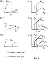
- the CDW memristor In the initial state, the CDW memristor is in the R HI state, and the superconducting channel in the R S 1 state. As the supercurrent increases, it follows the trajectory shown in Fig. 3e , 4e . At a critical value j c 1 , the superconductor element becomes resistive and follows the path up to the point where the current through the memristor exceeds j W . At this point the CDW memristor switches to R LO ( Fig. 4e ), effectively changing the shunt resistance, thus causing the superconducting channel to revert to the R S 2 state ( Fig. 3d, e and 4d, e ).
- the device is in the initial state R S 2 .
- Increasing the current causes it to follow the curve R S 2 until j E is reached through the CDW memristor shunt ( Fig. 3 d, f and Fig 4 d, f ).
- the CDW memristor reverts to the high resistance state R HI and the superconducting channel reverts to the state R S 1 ( Figs. 3 d, f and Fig 4 d, f ).
- critical currents and switching thresholds can be varied by appropriate design, thickness, widths of either channel.
- the two-terminal device is extended to a three-terminal configuration incorporating a superconductor on top of a memristive material, whereby an additional narrow choke is used to control the supercurrent in the narrow nanowire channel as demonstrated, but not limited to, the nano-cryotron (nTron) device described by McCaughan et al. (2014).
- an additional narrow choke is used to control the supercurrent in the narrow nanowire channel as demonstrated, but not limited to, the nano-cryotron (nTron) device described by McCaughan et al. (2014).
- the nTron described by McCaughan et al. (2014) is a thin-film superconducting device consisting of a gate nanowire and a channel nanowire with its two ends referred to as a drain and source.
- the intersection between the gate and the channel is referred as the choke.
- the choke is placed perpendicularly to where the channel is narrowest and the current density is the highest to maximize the sensitivity of the nTron.
- Current entering the gate terminal switches the phase of the choke from the superconducting to the resistive state when the local critical current density is exceeded. Breaking the superconductivity in a nanowire leads to the diffusion of hot quasiparticles and a growth of resistance.
- a current injection will flow through the memristor.
- the memristor and superconducting channel are not in direct contact, but are in electrical contact as shown in Fig. 1 , such that they are connected on the chip, the substrate or the contacts are configurable outside the chip.
- an array of memory devices substantially as described above can be set out, for example with a set of word lines and bit lines in a cross-bar configuration.
Landscapes
- Engineering & Computer Science (AREA)
- Chemical & Material Sciences (AREA)
- Computer Hardware Design (AREA)
- Crystallography & Structural Chemistry (AREA)
- Nanotechnology (AREA)
- Materials Engineering (AREA)
- Physics & Mathematics (AREA)
- Mathematical Physics (AREA)
- Theoretical Computer Science (AREA)
- Semiconductor Memories (AREA)
- Superconductor Devices And Manufacturing Methods Thereof (AREA)
Description
- The present invention relates to the technical field of memory devices and methods for the operation of such devices. The operation of memory devices at cryogenic temperatures enables the implementation of superconducting-based electronic devices and particularly, although not exclusively, to superconducting-based memory devices.
- In the view of the inventor, there is a need for a fast, low switching energy, cryogenic memory that is scalable, allows flexible architectures and is compatible with superconducting flux quantum electronics. Holmes et al. (2013) describe the requirements for fast and efficient operation of superconducting computers, emphasizing the need for fast efficient memory. The scalability and energy efficiency issues were discussed by Tolpygo (2016).
- An example of a known proposal for a memory solution is described by Zhao et al. (2018), who presented a superconducting nanowire memory element operated by nanowire cryotrons.
- Furthermore, various hybrid devices have been developed in the last decade. Ye et al. (2018) described a spin-transfer switching of orthogonal spin-valve devices at cryogenic temperatures. A hybrid superconducting-magnetic memory device using competing order parameters was described by Baek et al. (2014). Gingrich et al. described controllable 0-π Josephson junctions containing a ferromagnetic spin valve (Gingrich et al. 2016). Larkin et al. (2018) describe a ferromagnetic Josephson switching device with high characteristic voltage. A 380 ps, 9.5 mW Josephson 4-Kbit RAM that operated at a high bit yield was described by Nagasawa et al. (1995). A nanoscale superconducting memory based on the kinetic inductance of asymmetric nanowire loops was described by Murphy et al. (2017).
- Hybrid CMOS memory has been described most relevantly by Mukhanov et al. (2011) and Van Duzer et al. (2013). Mukhanov et al. (2011) described a hybrid semiconductor-superconductor fast memory based on CMOS. Van Duzer et al. (2013) described a 64-kb hybrid Josephson-CMOS 4 Kelvin RAM with 400 ps access time and 12 mW read power.
- Brenner, Roy, Shah and Bezryadin showed the dynamics of the superconducting nanowires shunted with an external resistor (Brenner et al. 2012). In their publication Baranov, Balanov and Kabanov theoretically showed the effect of shunt resistance on the dynamics of the resistive state in thin superconducting channels (Baranov et al. 2013). The effective resistance of a superconducting nanowire was described by Buh et al. (2015). Madan et al. (2018) presented optical switching of a superconducting nanowire resistance.
-
US2016035404 discloses a perpendicularly magnetized CSHE device that utilizes a magnetic tunnel junction (MTJ) and Nb superconducting contacts that connect to the spin Hall metal layer providing a low resistance write channel. - The present invention has been devised in light of the above considerations. The present invention is based in part on the inventor's realisation that it would be possible to implement a useful memory device that combines a switchable resistive element with a superconductor element to control the switching of the switchable resistive element.
- It is acknowledged that switchable resistive materials are known. Indeed, the present invention has been devised based in part on the inventor's previous work in this area. For example, resistance switching of such materials induced by light pulses or electrical pulses is described in
US 9,589,631 B2 US 9,818,479 B2 - Stojchevska et al. (2014) disclose low-temperature resistance switching in a charge density wave (CDW) material (1T-TaS2), by ultrashort laser pulses. Vaskivskyi et al. (2015) described low-temperature switching and resistivity relaxation by electrical pulses. In 2014 Stojchevska et al. and later in 2016 Vaskivskyi et al. showed switching by electrical pulses from 1 second to <50 ps (Stojchevska et al., 2014; Vaskivskyi et al., 2016), demonstrating write, read and erase operations. Such operation of a resistive switching device allows the device to be considered to be a "memristive" device in the sense that the device exhibits a resistance (detectable in a read operation) dependent on a previous electrical pulse applied to the device (e.g. a write or erase operation). The device disclosed by Vaskivskyi et al. (2016) showed scaling of switching voltage with device dimensions, enabling the device to be tailored to specific applications by appropriate choice of dimensions.
- Yoshida et al. (2015) described memristive behavior in 1T-TaS2 with liquid ion electrode gating.
- A superconducting-nanowire three-terminal electrothermal device (nanocryotron) was described by McCaughan et al. (2014) that uses a constriction (choke) to induce current-induced heating in a narrow superconducting channel to modulate the supercurrent in a thin-film superconducting device with a gate, a drain, and a source terminal, all connected contiguously with no junctions.
- Accordingly, in a first preferred aspect, the present invention provides a memory device according to the
independent device claim 1. - In a second preferred aspect, the present invention provides a method of operation of a memory device according to the method claim 12.
- The first and/or second aspect of the invention may have any one or, to the extent that they are compatible, any combination of the following optional features.
- Preferably the first and second resistive states of the active material represent first and second memory states of the switchable resistive element. As will be well understood, the first and second resistive states can be assigned binary values of 0 and 1, or 1 and 0, respectively, in order to store one bit of information.
- The memory device may either be a volatile memory device or a non-volatile memory device.
- The superconductor element may be in the form of a layer formed on an underlying substrate. For example, the superconducting element may be in the form of a film (thin film or thick film). The superconductor element may be patterned to form a required shape. For example, the superconductor element may be in the form of a nanowire. Here "nanowire" is intended to convey the requirement that at least one transverse dimension of the superconductor element is in the sub-micron range. More preferably, two orthogonal transverse dimensions (e.g. thickness and width) of the superconductor element may be in the sub-micron range.
- The superconductor element may be in the form of, or have, a narrow channel. Such a channel may for example include a constriction region. The constriction region may be adapted to switch from a superconducting state to a non-superconducting state, in preference to the remainder of the superconductor element, when the current flowing in the constriction exceeds the local critical current density or when the temperature of the constriction exceeds the critical temperature. In effect, the constriction region acts as a region of weakness for the current-carrying capability of the superconductor element.
- Switching into a non-superconducting state in the superconductor element causes the formation of a resistive region. Depending on the materials properties and dimensions of the resistive region (and the superconducting element as a whole), the resistive region may exhibit a resistance in the kΩ range. For example, suitable resistances of at least 0.1 kΩ, at least 1 kΩ or at least 10 kΩ may be exhibited.
- The switchable resistive element may be in the form of a layer formed on an underlying substrate. This may be the same substrate as for the superconducting element. For example, the switchable resistive element may be in the form of a film (thin film or thick film). The switchable resistive element may be patterned to form a required shape. For example, the switchable resistive element may be in the form of a nanowire.
- Preferably the superconductor element and the switchable resistive element are formed in a stacked arrangement. In the stacked arrangement, the superconductor element may be fabricated on top of the switchable resistive element, or vice versa, forming a parallel device.
- The superconductor element may be a two terminal device with positive and negative terminals (i.e. a source and a drain only, in analogy to transistor devices). Alternatively, the superconductor element may be a three-terminal device. Suitable three terminal superconducting elements are known, such as those in which an additional gate (in the form of a narrow choke) is used to control the current in the main part of the superconductor element between source and drain terminals. An example of such a three terminal superconducting element is disclosed and referred to as a "nano-cryotron" ("nTron") device by McCaughan et al. (2014).
- Turning now to the switchable resistive element, it is considered that suitable switching of resistivity states can take place with a current injection in the form of a current pulse with a duration of less than 1 µs, more preferably less than 100 ns, more preferably less than 50 ns, more preferably less than 20 ns.
- ρ1 can be expressed as X times ρ2. Preferably, X is at least 5, at least 10, at least 100 or more preferably at least 1000. As will be understood, provided that the difference between ρ1 and ρ2 can be determined reliably, then the memory device is able to store information based on that difference.
- The materials used for the active material of the switchable resistive element may be, but not limited to 1T-TaS2, a layered dichalcogenide, a chalcogenide or an oxide material. Suitable chalcogenide materials will now be set out in more detail. The active material may be formed from a layered dichalcogenide material. Suitable materials include 1T-TaS2 and 1T-TaSxSe2-x. It is at present considered that any material which supports multiple charge ordered states may be used in the present invention, including rare earth tri-tellurides. For example, it is considered at present that many materials support suitable macroscopic quantum states providing the required different resistivity states (such as CDW ordering). Suitable materials include: MX3 compounds (such as NbSe3, TaS3, NbS3, ZrTe3, etc.); transition metal tetrachalcogenides (MX4)nY (such as (TaSe4)2I, (NbSe4)3I,(NbSe4)10I3); blue and purple bronzes (K0.3MoO3, Rb0.3MoO3, TI0.3MoO3); molybdenum sub-oxides MoxOy, such as Mo4O11; O organic CDW systems such as Bechgaard-Fabre salts and TCNQ salts.
- The thickness of the active material is preferably less than 100 µm, e.g. less than 10 µm, more preferably less than 1 µm and still more preferably 500 nm or less. The active material may have a thickness of 1 nm or more, more preferably 5 nm or more, more preferably 10 nm or more. Corresponding dimensional ranges may also apply independently to the width of the active material.
- The temperature of operation of the device is primarily determined by the critical temperature Tc of the superconductor element. Suitable operating temperatures may therefore be 100K or lower, more typically for present materials 40K or lower. Temperatures of 20K or lower may be advantageous for some embodiments.
- Suitable materials for the superconductor element are known. For example, the superconductor element may comprise Nb, NbN or Al. At the temperature of operation, the superconductor is typically a type II superconductor. The device is preferably operated at a temperature of not greater than 2/3 times Tc (expressed in K) of the superconductor.
- Preferably, the current injection to the switchable resistive element is achieved at relatively low voltage. The preferred arrangement is for the current injection to be achieved at transistor logic levels. For example, preferably the current injection is achieved at voltage of 20V or less, more preferably 12V or less, more preferably 10V or less, more preferably 8V or less, more preferably 6V or less, more preferably 4V or less, more preferably below 1V. In terms of electric field strength, preferably the current injection is achieved at electric field strength of 200 kV/cm or less, more preferably 50 kV/cm or less, more preferably 30 kV/cm or less, more preferably 25 kV/cm or less, more preferably 12 kV/cm or less, more preferably 15 kV/cm or less, more preferably about 10 kV/cm.
- Preferably the current injection to the device is provided, in use, by an external circuit. The current injection may either be in a pulsed mode or in a continuous mode and may be achieved by control of an applied current to the device or by control of an applied voltage across the device.
- The invention includes the combination of the aspects and preferred features described except where such a combination is clearly impermissible or expressly avoided. Further optional features of the invention are set out below.
- Embodiments and experiments illustrating the principles of the invention will now be discussed with reference to the accompanying figures in which:
-
Figure 1 . An effective simplified circuit diagram of the 'parallelotron' or 'p-tron' device, includingsuperconductor element 1 and switchableresistive element 2 in physical contact or connected electrically via external circuit to the superconductor element. -
Figure 2 . Schematic of asuperconductor element 3 fabricated on top of a switchableresistive element 2 forming a parallel device onsubstrate 5. Aconstriction 6 in thesuperconductor element 3 serves to locally increase the current density and create ahot spot 7 where the current density is sufficient to cause a superconductor-to-normal state transition which then causes part of the current to flow through the switchableresistive element 4. -
Figure 3 . The behaviour of a switchable resistive element according to Vaskivskyi et al. (2016). a) The V-j curve for a switchable resistive element Write cycle. b) The V-j curve for the Erase cycle. c) The V-j curves corresponding to the RHI and RLO states of the switchable resistive material. d) The V-j curves R S1 and R S2 for a superconductor nanowire with high (RHI ) and low (RLO ) shunt resistances respectively, jc is the superconducting critical current. e) The Write cycle for a nanowire weak link with a switchable resistive element switching from RHI to RLO at or above a threshold current jW. f) The Erase cycle for a nanowire weak link with a switchable resistive element shunt switching from RLO to RHI at or above a threshold current jE . -
Figure 4 . SupplementsFigure 3 to show a) The V-j curve for a switchable resistive element Write cycle. b) The V-j curve for the Erase cycle. c) The V-j curves corresponding to the RHI and RLO states of the switchable resistive material. d) The V-j curves R S1 and R S2 for a superconductor nanowire with high (RHI ) and low (RLO ) shunt resistances respectively e) The V-j curves for; the Write cycle for a switchable resistive element, a superconductor nanowire with resistance R S1 and R S2 with high (RHI ) and low (RLO ) shunt resistances respectively, the Write cycle for a nanowire weak link with a switchable resistive element switching from RHI to RLO at or above a threshold current jW. - Aspects and embodiments of the present invention will now be discussed with reference to the accompanying figures. Further aspects and embodiments will be apparent to those skilled in the art.
- In a general overview, it can be seen that the preferred embodiments of the invention provide a hybrid superconducting memory device that combines a superconductor element in parallel with a switchable resistive element. The preferred embodiments are characterized by ultrafast switching speed, two- or three-terminal operation, scalability, low switching energy (due to the ability to use low-energy memristive elements), low-temperature operation, ease of integration, simple 2-element circuit design and compatibility with superconducting electronics, particularly superconducting flux-quantum electronics. The basic device in one embodiment is composed of a superconductor element on top of a switchable resistive element, effectively forming a narrow superconducting channel shunted with a controllable resistance shunt. An effective circuit diagram of the device is shown in
Fig. 1 . The shunt resistance is Rs which is switchable (non-volatile), or a non-linear element that acts as a variable or non-linear shunt resistance. - Typically, a constriction is fabricated in the superconducting channel such that the current density is higher at a selected region in the channel as shown in
Fig. 2 . - The device consists of a narrow superconductor channel deposited on a memristive non-volatile CDW material described previously (
US9818479 (B2 - The reverse transition from the low resistance state to the high resistance state of the shunt memristor (the Erase operation) is caused when the current exceeds a certain but different value of critical current j c2, changing the shunt resistance to a high value. A geometrical constriction in the memristive material may be used to confine and tailor the current path through the memristive material. The detailed operation of a preferred embodiment of the device is described below.
- The operation cycles are shown in
Figs. 3 a-c andFigs 4 a-c , describing the Write, Erase and read cycles of a CDW memristor, as described by Vaskivskyi et al. (2016). - In the Write cycle (
Fig. 3a andFig. 4a ) the device is initially in a high resistance state RHI , in which the current-voltage (j-V) curve is approximately described by j = j 0 exp(V/V0 ), where j 0 and V 0 are constants (Vaskivskyi et al., 2016). Above a threshold current jW , the resistance drops to a low resistance state RLO , remaining in this state indefinitely, i.e. as long as the memristor remains in the low-resistance state as determined by external factors, such as the state lifetime, or temperature. - The Erase cycle (
Fig. 3b andFig. 4b ) involves increasing the current in the low-resistance state RLO of the CDW memristor until an Erase threshold is reached (jE ). Upon reducing the current, the original high-resistance state RHI is recovered. - Read operations in the RHI and RLO states are shown in
Fig. 3c andFig. 4c . - The operation of the nanowire channel shunted by a fixed resistance Rs as shown in
Fig. 1 is described by Brenner et al. (2012) and is shown inFig. 3d andFig. 4d for two different values of R s1 and R s2. For Rs > Rcritical , where Rcritical is some critical resistance value, the device shows hysteretic V-I behavior. When Rs < Rcritical , the device shows no hysteresis and a lower overall resistance, with a higher critical current value. - In the initial state, the CDW memristor is in the RHI state, and the superconducting channel in the R S1 state. As the supercurrent increases, it follows the trajectory shown in
Fig. 3e ,4e . At a critical value j c1, the superconductor element becomes resistive and follows the path up to the point where the current through the memristor exceeds jW . At this point the CDW memristor switches to RLO (Fig. 4e ), effectively changing the shunt resistance, thus causing the superconducting channel to revert to the R S2 state (Fig. 3d, e and4d, e ). - The device is in the initial state R S2. Increasing the current causes it to follow the curve R S2 until jE is reached through the CDW memristor shunt (
Fig. 3 d, f andFig 4 d, f ). Upon reducing the current, the CDW memristor reverts to the high resistance state RHI and the superconducting channel reverts to the state R S1 (Figs. 3 d, f andFig 4 d, f ). - The values of critical currents and switching thresholds can be varied by appropriate design, thickness, widths of either channel.
- In another embodiment, the two-terminal device is extended to a three-terminal configuration incorporating a superconductor on top of a memristive material, whereby an additional narrow choke is used to control the supercurrent in the narrow nanowire channel as demonstrated, but not limited to, the nano-cryotron (nTron) device described by McCaughan et al. (2014).
- The nTron described by McCaughan et al. (2014) is a thin-film superconducting device consisting of a gate nanowire and a channel nanowire with its two ends referred to as a drain and source. The intersection between the gate and the channel is referred as the choke. The choke is placed perpendicularly to where the channel is narrowest and the current density is the highest to maximize the sensitivity of the nTron. Current entering the gate terminal switches the phase of the choke from the superconducting to the resistive state when the local critical current density is exceeded. Breaking the superconductivity in a nanowire leads to the diffusion of hot quasiparticles and a growth of resistance. In the present invention, when the nTron channel switches to a resistive state, a current injection will flow through the memristor.
- In a further embodiment of the device, the memristor and superconducting channel are not in direct contact, but are in electrical contact as shown in
Fig. 1 , such that they are connected on the chip, the substrate or the contacts are configurable outside the chip. - In a further configuration, an array of memory devices substantially as described above can be set out, for example with a set of word lines and bit lines in a cross-bar configuration.
- The features disclosed in the foregoing description, or in the following claims, or in the accompanying drawings, expressed in their specific forms or in terms of a means for performing the disclosed function, or a method or process for obtaining the disclosed results, as appropriate, may, separately, or in any combination of such features, be utilised for realising the invention in diverse forms thereof.
- While the invention has been described in conjunction with the exemplary embodiments described above, many equivalent modifications and variations will be apparent to those skilled in the art when given this disclosure. Accordingly, the exemplary embodiments of the invention set forth above are considered to be illustrative and not limiting. Various changes to the described embodiments may be made without departing from the scope of the invention as defined by the claims.
- For the avoidance of any doubt, any theoretical explanations provided herein are provided for the purposes of improving the understanding of a reader. The inventors do not wish to be bound by any of these theoretical explanations.
- Any section headings used herein are for organizational purposes only and are not to be construed as limiting the subject matter described.
- Throughout this specification, including the claims which follow, unless the context requires otherwise, the word "comprise" and "include", and variations such as "comprises", "comprising", and "including" will be understood to imply the inclusion of a stated integer or step or group of integers or steps but not the exclusion of any other integer or step or group of integers or steps.
- It must be noted that, as used in the specification and the appended claims, the singular forms "a," "an," and "the" include plural referents unless the context clearly dictates otherwise. Ranges may be expressed herein as from "about" one particular value, and/or to "about" another particular value. When such a range is expressed, another embodiment includes from the one particular value and/or to the other particular value. Similarly, when values are expressed as approximations, by the use of the antecedent "about," it will be understood that the particular value forms another embodiment. The term "about" in relation to a numerical value is optional and means for example +/- 10%.
- A number of publications are cited above in order to more fully describe and disclose the invention and the state of the art to which the invention pertains. Full citations for these references are provided below.
- D.S. Holmes et al. Energy-Efficient Superconducting Computing-Power Budgets and Requirements, IEEE transactions on Appl. Supercon. 23, 1701610 (2013).
- S. K. Tolpygo. Superconductor Digital Electronics: Scalability and Energy Efficiency Issues. Low Temperature Physics, vol. 42, ).
- Q.-Y. Zhao et al. A compact superconducting nanowire memory element operated by nanowire cryotrons. Supercond. Sci. Technol. 31 (2018).
- L. Ye et al. Spin-transfer switching of orthogonal spin-valve devices at cryogenic temperatures. Journal of Applied Physics 115, 17C725 (2014).
- B. Baek et al. Hybrid superconducting-magnetic memory device using competing order parameters. ).
- E. C. Gingrich et al. Controllable 0-π Josephson junctions containing a ferromagnetic spin valve. Nature Physics volume 12, pages 564-567 (2016).
- T.I. Larkin et al. Ferromagnetic Josephson switching device with high characteristic voltage. Appl. Phys. Lett. 100, 222601 (2012).
- S. Nagasawa et al. A 380 ps, 9.5 mW Josephson 4-Kbit RAM operated at a high bit yield. IEEE Transactions on Applied Superconductivity (Volume: 5 , Issue: 2 , June 1995).
- A. Murphy et al. Nanoscale superconducting memory based on the kinetic inductance of asymmetric nanowire loops. New J. Phys. 19, 063015 (2017).
- O. A. Mukhanov et al. Hybrid Semiconductor-Superconductor Fast-Readout Memory for Digital RF Receivers. IEEE Transactions on Applied Superconductivity (Volume: 21 , Issue: 3 , June 2011).
- T. Van Duzer et al. 64-kb Hybrid Josephson-).
- M. W. Brenner et al. Dynamics of superconducting nanowires shunted with an external resistor. Phys. Rev. B 85, 224507 (2012).
- V. V. Baranov et al. Dynamics of resistive state in thin superconducting channels. Physical review. B, Condensed matter 87(17):174516 (2013).
- J. Buh et al. Control of switching between metastable superconducting states in δ-MοN nanowires. Nat Commun. 6: 10250 (2015).
- I. Madan et al. Nonequilibrium optical control of dynamical states in superconducting nanowire circuits. Science Advances. Vol. 4, no. 3. (2018).
-
US 9,589,631 B2 -
US 9,818,479 B2 - L. Stojchevska et al. Ultrafast Switching to a Stable Hidden Quantum State in an Electronic Crystal. Science. Vol. 344, Issue 6180, pp. 177-180. (2014).
- I. Vaskivskyi et al. Controlling the metal-to-insulator relaxation of the metastable hidden quantum state in 1T-TaS2. Science Advances. Vol. 1, no. 6. (2015).
- I. Vaskivskyi et al. Fast electronic resistance switching involving hidden charge density wave states. ).
- M. Yoshida et al. Memristive phase switching in two-dimensional 1T-TaS2 crystals. Sci Adv. 1(9). (2015).
- A. N. McCaughan et al. A Superconducting-Nanowire Three-Terminal Electrothermal Device. Nano Lett., 14 (10), pp 5748-5753, (2014).
Claims (15)
- A memory device comprising:a switchable resistive element (2) comprising an active material, the active material being switchable, by current injection, between first and second values of electrical resistivity ρ1 and ρ2 at the same temperature, wherein ρ1 is different to ρ2; anda superconductor element (1) connected electrically in parallel with the switchable resistive element (2), the superconductor element (1) being operable so that at least part of the superconductor element is switchable from a superconducting state to a non-superconducting state,characterized in thatthe memory device is configured to operate so that, when the superconductor element (1) is switched from the superconducting state to the non-superconducting state by current density, a current injection is provided through the switchable resistive element (2) thereby switching the switchable resistive element between said first and second values of electrical resistivity, and wherein the active material of the switchable resistive element is a memristive nonvolatile charge density wave material.
- A memory device according to claim 1 wherein the first and second resistive states of the active material represent first and second memory states of the switchable resistive element (2).
- A memory device according to claim 1 or claim 2 wherein the memory device is a volatile memory device.
- A memory device according to claim 1 or claim 2 wherein the memory device is a non-volatile memory device.
- A memory device according to any one of claims 1 to 4 wherein the superconductor is in the form of a nanowire or a narrow channel.
- A memory device according to any one of claims 1 to 5 wherein the superconductor element (1) includes a constriction region (6) adapted to switch to a non-superconducting state in preference to the remainder of the superconductor element.
- A memory device according to any one of claims 1 to 6 wherein the superconductor element (1) and the switchable resistive element (2) are formed in a stacked arrangement.
- A memory device according to any one of claims 1 to 7 wherein the superconductor element (1) is a two terminal device.
- A memory device according to any one of claims 1 to 7 wherein the superconductor element (1) is a three terminal device.
- A memory device according to any one of claims 1 to 9 wherein the active material of the switchable resistive element (2) is 1T-TaS2, a layered dichalcogenide, a chalcogenide or an oxide material.
- A memory device according to any one of claims 1 to 10 wherein the current injection is provided, in use, by an external circuit.
- A method of operation of a memory device according to any one of claims 1-11, the method including the steps:providing a temperature environment for at least the superconductor element (1) to allow at least part of the superconductor element (1) to be in a superconducting state; andswitching at least part of the superconductor element (1) from the superconducting state to a non-superconducting state and thereby causing a current injection to flow through the switchable resistive element (2) capable of switching the switchable resistive element (2) between said first and second values of electrical resistivity,characterized in thatat least part of the superconductor element (1) is switched from a superconducting state to a non-superconducting state by current density.
- A method according to claim 12 wherein the current injection is in a pulsed mode.
- A method according to claim 12 wherein the current injection is in a continuous mode.
- A method according to any one of claims 12 to 14 wherein the current injection is achieved by control of an applied current to the device or by control of an applied voltage across the device.
Applications Claiming Priority (2)
| Application Number | Priority Date | Filing Date | Title |
|---|---|---|---|
| GB1818713.8A GB2579058A (en) | 2018-11-16 | 2018-11-16 | Memory device and method for its operation |
| PCT/EP2019/081375 WO2020099584A1 (en) | 2018-11-16 | 2019-11-14 | Memory device and method for its operation |
Publications (2)
| Publication Number | Publication Date |
|---|---|
| EP3881365A1 EP3881365A1 (en) | 2021-09-22 |
| EP3881365B1 true EP3881365B1 (en) | 2023-01-11 |
Family
ID=64740161
Family Applications (1)
| Application Number | Title | Priority Date | Filing Date |
|---|---|---|---|
| EP19805621.0A Active EP3881365B1 (en) | 2018-11-16 | 2019-11-14 | Memory device and method for its operation |
Country Status (4)
| Country | Link |
|---|---|
| US (1) | US11756609B2 (en) |
| EP (1) | EP3881365B1 (en) |
| GB (1) | GB2579058A (en) |
| WO (1) | WO2020099584A1 (en) |
Family Cites Families (13)
| Publication number | Priority date | Publication date | Assignee | Title |
|---|---|---|---|---|
| US4275314A (en) * | 1979-04-30 | 1981-06-23 | Bell Telephone Laboratories, Incorporated | Josephson Atto-Weber switch |
| JPH071866B2 (en) * | 1984-09-25 | 1995-01-11 | 日本電気株式会社 | Resistive coupling type Josephson logic circuit |
| JPS6288381A (en) * | 1985-10-11 | 1987-04-22 | インタ−ナショナル ビジネス マシ−ンズ コ−ポレ−ション | Superconducting switching apparatus |
| JPH04129426A (en) * | 1990-09-20 | 1992-04-30 | Res Dev Corp Of Japan | Superconducting digital analog converter |
| US5629889A (en) * | 1995-12-14 | 1997-05-13 | Nec Research Institute, Inc. | Superconducting fault-tolerant programmable memory cell incorporating Josephson junctions |
| US7038935B2 (en) * | 2002-08-02 | 2006-05-02 | Unity Semiconductor Corporation | 2-terminal trapped charge memory device with voltage switchable multi-level resistance |
| KR20140021544A (en) * | 2011-01-26 | 2014-02-20 | 이큐비트, 아이엔씨. | Josephson magnetic switch |
| SI24265A (en) | 2012-11-30 | 2014-06-30 | Institut "Jožef Stefan" | Ultrafast quench based nonvolatile bistable device |
| GB201412884D0 (en) | 2014-07-21 | 2014-09-03 | Inst Jozef Stefan | Switchable macroscopic quantum state devices and methods for their operation |
| US9552862B2 (en) * | 2014-07-29 | 2017-01-24 | Raytheon Bbn Technologies Corp. | Magnetic ram array architecture |
| CN107819070B (en) * | 2017-11-23 | 2020-04-21 | 上海新储集成电路有限公司 | Preparation method of phase change memory with 1D1R superconducting electrode material structure |
| US10984857B2 (en) * | 2018-08-16 | 2021-04-20 | PsiQuantum Corp. | Superconductive memory cells and devices |
| US10923646B2 (en) * | 2018-11-30 | 2021-02-16 | Microsoft Technology Licensing, Llc | Superconducting switch having a persistent and a non-persistent state |
-
2018
- 2018-11-16 GB GB1818713.8A patent/GB2579058A/en not_active Withdrawn
-
2019
- 2019-11-14 WO PCT/EP2019/081375 patent/WO2020099584A1/en not_active Ceased
- 2019-11-14 EP EP19805621.0A patent/EP3881365B1/en active Active
- 2019-11-14 US US17/293,693 patent/US11756609B2/en active Active
Also Published As
| Publication number | Publication date |
|---|---|
| US20220005524A1 (en) | 2022-01-06 |
| GB2579058A (en) | 2020-06-10 |
| US11756609B2 (en) | 2023-09-12 |
| WO2020099584A1 (en) | 2020-05-22 |
| GB201818713D0 (en) | 2019-01-02 |
| EP3881365A1 (en) | 2021-09-22 |
Similar Documents
| Publication | Publication Date | Title |
|---|---|---|
| Alam et al. | Cryogenic memory technologies | |
| Yang et al. | Memristive devices in computing system: Promises and challenges | |
| TWI713585B (en) | Method, system and device for complementary non-volatile memory device operation (2) | |
| Di Ventra et al. | Memory materials: a unifying description | |
| Wang et al. | Overview of emerging memristor families from resistive memristor to spintronic memristor | |
| CN107689799B (en) | Switching device with non-linear element | |
| Yang et al. | A family of electronically reconfigurable nanodevices | |
| CN103168372B (en) | There is the combination of the memory cell of resistance switch layer | |
| US20150053909A1 (en) | Nonlinear memristors | |
| Yoo et al. | Steep slope field-effect transistors with B–Te-based ovonic threshold switch device | |
| TW201626507A (en) | Memory cell array | |
| Palau et al. | Electrochemical tuning of metal insulator transition and nonvolatile resistive switching in superconducting films | |
| US10964748B1 (en) | Electric field controllable spin filter tunnel junction magnetoresistive memory devices and methods of making the same | |
| US11069741B2 (en) | Electric field controllable spin filter tunnel junction magnetoresistive memory devices and methods of making the same | |
| Yoshida et al. | Unipolar resistive switching in CoFeB∕ MgO∕ CoFeB magnetic tunnel junction | |
| Tulina | Colossal electroresistance and electron instability in strongly correlated electron systems | |
| US11756609B2 (en) | Memory device and method for its operation | |
| Mehonic et al. | Resistive switching in oxides | |
| CN113243052B (en) | Spin filter tunnel junction magnetoresistive memory device with controllable electric field and method of fabricating the same | |
| Song et al. | Selector devices for x-point memory | |
| EP4453938B1 (en) | Superconducting bipolar thermoelectric memory and method for writing a superconducting bipolar thermoelectric memory | |
| Subin et al. | Resistive switching in metal oxides for various applications | |
| Yang et al. | Coupled interfaces for misreading avoidance and write current reduction in passive crossbar memory | |
| Yang et al. | Oxide based memristive devices | |
| Lee et al. | Investigation of a selective switching device using a phase-change material for a 3-dimensional PCRAM array |
Legal Events
| Date | Code | Title | Description |
|---|---|---|---|
| STAA | Information on the status of an ep patent application or granted ep patent |
Free format text: STATUS: UNKNOWN |
|
| STAA | Information on the status of an ep patent application or granted ep patent |
Free format text: STATUS: THE INTERNATIONAL PUBLICATION HAS BEEN MADE |
|
| PUAI | Public reference made under article 153(3) epc to a published international application that has entered the european phase |
Free format text: ORIGINAL CODE: 0009012 |
|
| STAA | Information on the status of an ep patent application or granted ep patent |
Free format text: STATUS: REQUEST FOR EXAMINATION WAS MADE |
|
| 17P | Request for examination filed |
Effective date: 20210505 |
|
| AK | Designated contracting states |
Kind code of ref document: A1 Designated state(s): AL AT BE BG CH CY CZ DE DK EE ES FI FR GB GR HR HU IE IS IT LI LT LU LV MC MK MT NL NO PL PT RO RS SE SI SK SM TR |
|
| DAV | Request for validation of the european patent (deleted) | ||
| DAX | Request for extension of the european patent (deleted) | ||
| GRAP | Despatch of communication of intention to grant a patent |
Free format text: ORIGINAL CODE: EPIDOSNIGR1 |
|
| STAA | Information on the status of an ep patent application or granted ep patent |
Free format text: STATUS: GRANT OF PATENT IS INTENDED |
|
| INTG | Intention to grant announced |
Effective date: 20220726 |
|
| GRAS | Grant fee paid |
Free format text: ORIGINAL CODE: EPIDOSNIGR3 |
|
| GRAA | (expected) grant |
Free format text: ORIGINAL CODE: 0009210 |
|
| STAA | Information on the status of an ep patent application or granted ep patent |
Free format text: STATUS: THE PATENT HAS BEEN GRANTED |
|
| AK | Designated contracting states |
Kind code of ref document: B1 Designated state(s): AL AT BE BG CH CY CZ DE DK EE ES FI FR GB GR HR HU IE IS IT LI LT LU LV MC MK MT NL NO PL PT RO RS SE SI SK SM TR |
|
| REG | Reference to a national code |
Ref country code: GB Ref legal event code: FG4D |
|
| REG | Reference to a national code |
Ref country code: CH Ref legal event code: EP |
|
| REG | Reference to a national code |
Ref country code: DE Ref legal event code: R096 Ref document number: 602019024370 Country of ref document: DE |
|
| REG | Reference to a national code |
Ref country code: IE Ref legal event code: FG4D |
|
| REG | Reference to a national code |
Ref country code: AT Ref legal event code: REF Ref document number: 1543940 Country of ref document: AT Kind code of ref document: T Effective date: 20230215 |
|
| REG | Reference to a national code |
Ref country code: NL Ref legal event code: FP |
|
| REG | Reference to a national code |
Ref country code: LT Ref legal event code: MG9D |
|
| REG | Reference to a national code |
Ref country code: AT Ref legal event code: MK05 Ref document number: 1543940 Country of ref document: AT Kind code of ref document: T Effective date: 20230111 |
|
| PG25 | Lapsed in a contracting state [announced via postgrant information from national office to epo] |
Ref country code: RS Free format text: LAPSE BECAUSE OF FAILURE TO SUBMIT A TRANSLATION OF THE DESCRIPTION OR TO PAY THE FEE WITHIN THE PRESCRIBED TIME-LIMIT Effective date: 20230111 Ref country code: PT Free format text: LAPSE BECAUSE OF FAILURE TO SUBMIT A TRANSLATION OF THE DESCRIPTION OR TO PAY THE FEE WITHIN THE PRESCRIBED TIME-LIMIT Effective date: 20230511 Ref country code: NO Free format text: LAPSE BECAUSE OF FAILURE TO SUBMIT A TRANSLATION OF THE DESCRIPTION OR TO PAY THE FEE WITHIN THE PRESCRIBED TIME-LIMIT Effective date: 20230411 Ref country code: LV Free format text: LAPSE BECAUSE OF FAILURE TO SUBMIT A TRANSLATION OF THE DESCRIPTION OR TO PAY THE FEE WITHIN THE PRESCRIBED TIME-LIMIT Effective date: 20230111 Ref country code: LT Free format text: LAPSE BECAUSE OF FAILURE TO SUBMIT A TRANSLATION OF THE DESCRIPTION OR TO PAY THE FEE WITHIN THE PRESCRIBED TIME-LIMIT Effective date: 20230111 Ref country code: HR Free format text: LAPSE BECAUSE OF FAILURE TO SUBMIT A TRANSLATION OF THE DESCRIPTION OR TO PAY THE FEE WITHIN THE PRESCRIBED TIME-LIMIT Effective date: 20230111 Ref country code: ES Free format text: LAPSE BECAUSE OF FAILURE TO SUBMIT A TRANSLATION OF THE DESCRIPTION OR TO PAY THE FEE WITHIN THE PRESCRIBED TIME-LIMIT Effective date: 20230111 Ref country code: AT Free format text: LAPSE BECAUSE OF FAILURE TO SUBMIT A TRANSLATION OF THE DESCRIPTION OR TO PAY THE FEE WITHIN THE PRESCRIBED TIME-LIMIT Effective date: 20230111 |
|
| PG25 | Lapsed in a contracting state [announced via postgrant information from national office to epo] |
Ref country code: SE Free format text: LAPSE BECAUSE OF FAILURE TO SUBMIT A TRANSLATION OF THE DESCRIPTION OR TO PAY THE FEE WITHIN THE PRESCRIBED TIME-LIMIT Effective date: 20230111 Ref country code: PL Free format text: LAPSE BECAUSE OF FAILURE TO SUBMIT A TRANSLATION OF THE DESCRIPTION OR TO PAY THE FEE WITHIN THE PRESCRIBED TIME-LIMIT Effective date: 20230111 Ref country code: IS Free format text: LAPSE BECAUSE OF FAILURE TO SUBMIT A TRANSLATION OF THE DESCRIPTION OR TO PAY THE FEE WITHIN THE PRESCRIBED TIME-LIMIT Effective date: 20230511 Ref country code: GR Free format text: LAPSE BECAUSE OF FAILURE TO SUBMIT A TRANSLATION OF THE DESCRIPTION OR TO PAY THE FEE WITHIN THE PRESCRIBED TIME-LIMIT Effective date: 20230412 Ref country code: FI Free format text: LAPSE BECAUSE OF FAILURE TO SUBMIT A TRANSLATION OF THE DESCRIPTION OR TO PAY THE FEE WITHIN THE PRESCRIBED TIME-LIMIT Effective date: 20230111 |
|
| REG | Reference to a national code |
Ref country code: DE Ref legal event code: R097 Ref document number: 602019024370 Country of ref document: DE |
|
| PG25 | Lapsed in a contracting state [announced via postgrant information from national office to epo] |
Ref country code: SM Free format text: LAPSE BECAUSE OF FAILURE TO SUBMIT A TRANSLATION OF THE DESCRIPTION OR TO PAY THE FEE WITHIN THE PRESCRIBED TIME-LIMIT Effective date: 20230111 Ref country code: RO Free format text: LAPSE BECAUSE OF FAILURE TO SUBMIT A TRANSLATION OF THE DESCRIPTION OR TO PAY THE FEE WITHIN THE PRESCRIBED TIME-LIMIT Effective date: 20230111 Ref country code: EE Free format text: LAPSE BECAUSE OF FAILURE TO SUBMIT A TRANSLATION OF THE DESCRIPTION OR TO PAY THE FEE WITHIN THE PRESCRIBED TIME-LIMIT Effective date: 20230111 Ref country code: DK Free format text: LAPSE BECAUSE OF FAILURE TO SUBMIT A TRANSLATION OF THE DESCRIPTION OR TO PAY THE FEE WITHIN THE PRESCRIBED TIME-LIMIT Effective date: 20230111 Ref country code: CZ Free format text: LAPSE BECAUSE OF FAILURE TO SUBMIT A TRANSLATION OF THE DESCRIPTION OR TO PAY THE FEE WITHIN THE PRESCRIBED TIME-LIMIT Effective date: 20230111 |
|
| PLBE | No opposition filed within time limit |
Free format text: ORIGINAL CODE: 0009261 |
|
| STAA | Information on the status of an ep patent application or granted ep patent |
Free format text: STATUS: NO OPPOSITION FILED WITHIN TIME LIMIT |
|
| PG25 | Lapsed in a contracting state [announced via postgrant information from national office to epo] |
Ref country code: SK Free format text: LAPSE BECAUSE OF FAILURE TO SUBMIT A TRANSLATION OF THE DESCRIPTION OR TO PAY THE FEE WITHIN THE PRESCRIBED TIME-LIMIT Effective date: 20230111 |
|
| 26N | No opposition filed |
Effective date: 20231012 |
|
| PG25 | Lapsed in a contracting state [announced via postgrant information from national office to epo] |
Ref country code: SI Free format text: LAPSE BECAUSE OF FAILURE TO SUBMIT A TRANSLATION OF THE DESCRIPTION OR TO PAY THE FEE WITHIN THE PRESCRIBED TIME-LIMIT Effective date: 20230111 |
|
| PG25 | Lapsed in a contracting state [announced via postgrant information from national office to epo] |
Ref country code: IT Free format text: LAPSE BECAUSE OF FAILURE TO SUBMIT A TRANSLATION OF THE DESCRIPTION OR TO PAY THE FEE WITHIN THE PRESCRIBED TIME-LIMIT Effective date: 20230111 |
|
| PG25 | Lapsed in a contracting state [announced via postgrant information from national office to epo] |
Ref country code: MC Free format text: LAPSE BECAUSE OF FAILURE TO SUBMIT A TRANSLATION OF THE DESCRIPTION OR TO PAY THE FEE WITHIN THE PRESCRIBED TIME-LIMIT Effective date: 20230111 |
|
| PG25 | Lapsed in a contracting state [announced via postgrant information from national office to epo] |
Ref country code: LU Free format text: LAPSE BECAUSE OF NON-PAYMENT OF DUE FEES Effective date: 20231114 |
|
| PG25 | Lapsed in a contracting state [announced via postgrant information from national office to epo] |
Ref country code: MC Free format text: LAPSE BECAUSE OF FAILURE TO SUBMIT A TRANSLATION OF THE DESCRIPTION OR TO PAY THE FEE WITHIN THE PRESCRIBED TIME-LIMIT Effective date: 20230111 Ref country code: LU Free format text: LAPSE BECAUSE OF NON-PAYMENT OF DUE FEES Effective date: 20231114 |
|
| REG | Reference to a national code |
Ref country code: BE Ref legal event code: MM Effective date: 20231130 |
|
| REG | Reference to a national code |
Ref country code: IE Ref legal event code: MM4A |
|
| PG25 | Lapsed in a contracting state [announced via postgrant information from national office to epo] |
Ref country code: IE Free format text: LAPSE BECAUSE OF NON-PAYMENT OF DUE FEES Effective date: 20231114 |
|
| PG25 | Lapsed in a contracting state [announced via postgrant information from national office to epo] |
Ref country code: BE Free format text: LAPSE BECAUSE OF NON-PAYMENT OF DUE FEES Effective date: 20231130 |
|
| PG25 | Lapsed in a contracting state [announced via postgrant information from national office to epo] |
Ref country code: IE Free format text: LAPSE BECAUSE OF NON-PAYMENT OF DUE FEES Effective date: 20231114 Ref country code: BE Free format text: LAPSE BECAUSE OF NON-PAYMENT OF DUE FEES Effective date: 20231130 |
|
| PG25 | Lapsed in a contracting state [announced via postgrant information from national office to epo] |
Ref country code: BG Free format text: LAPSE BECAUSE OF FAILURE TO SUBMIT A TRANSLATION OF THE DESCRIPTION OR TO PAY THE FEE WITHIN THE PRESCRIBED TIME-LIMIT Effective date: 20230111 |
|
| PG25 | Lapsed in a contracting state [announced via postgrant information from national office to epo] |
Ref country code: BG Free format text: LAPSE BECAUSE OF FAILURE TO SUBMIT A TRANSLATION OF THE DESCRIPTION OR TO PAY THE FEE WITHIN THE PRESCRIBED TIME-LIMIT Effective date: 20230111 |
|
| PG25 | Lapsed in a contracting state [announced via postgrant information from national office to epo] |
Ref country code: CY Free format text: LAPSE BECAUSE OF FAILURE TO SUBMIT A TRANSLATION OF THE DESCRIPTION OR TO PAY THE FEE WITHIN THE PRESCRIBED TIME-LIMIT; INVALID AB INITIO Effective date: 20191114 |
|
| PG25 | Lapsed in a contracting state [announced via postgrant information from national office to epo] |
Ref country code: HU Free format text: LAPSE BECAUSE OF FAILURE TO SUBMIT A TRANSLATION OF THE DESCRIPTION OR TO PAY THE FEE WITHIN THE PRESCRIBED TIME-LIMIT; INVALID AB INITIO Effective date: 20191114 |
|
| PGFP | Annual fee paid to national office [announced via postgrant information from national office to epo] |
Ref country code: NL Payment date: 20251021 Year of fee payment: 7 |
|
| REG | Reference to a national code |
Ref country code: CH Ref legal event code: U11 Free format text: ST27 STATUS EVENT CODE: U-0-0-U10-U11 (AS PROVIDED BY THE NATIONAL OFFICE) Effective date: 20251201 |
|
| PG25 | Lapsed in a contracting state [announced via postgrant information from national office to epo] |
Ref country code: TR Free format text: LAPSE BECAUSE OF FAILURE TO SUBMIT A TRANSLATION OF THE DESCRIPTION OR TO PAY THE FEE WITHIN THE PRESCRIBED TIME-LIMIT Effective date: 20230111 |
|
| PGFP | Annual fee paid to national office [announced via postgrant information from national office to epo] |
Ref country code: DE Payment date: 20251119 Year of fee payment: 7 |
|
| PGFP | Annual fee paid to national office [announced via postgrant information from national office to epo] |
Ref country code: GB Payment date: 20251119 Year of fee payment: 7 |
|
| PGFP | Annual fee paid to national office [announced via postgrant information from national office to epo] |
Ref country code: FR Payment date: 20251119 Year of fee payment: 7 |
|
| PGFP | Annual fee paid to national office [announced via postgrant information from national office to epo] |
Ref country code: CH Payment date: 20251201 Year of fee payment: 7 |