EP3880471B1 - Decoration film and electronic device including the same - Google Patents
Decoration film and electronic device including the same Download PDFInfo
- Publication number
- EP3880471B1 EP3880471B1 EP19898949.3A EP19898949A EP3880471B1 EP 3880471 B1 EP3880471 B1 EP 3880471B1 EP 19898949 A EP19898949 A EP 19898949A EP 3880471 B1 EP3880471 B1 EP 3880471B1
- Authority
- EP
- European Patent Office
- Prior art keywords
- layer
- color
- shape
- electronic device
- cured
- Prior art date
- Legal status (The legal status is an assumption and is not a legal conclusion. Google has not performed a legal analysis and makes no representation as to the accuracy of the status listed.)
- Active
Links
Images



Classifications
-
- B—PERFORMING OPERATIONS; TRANSPORTING
- B32—LAYERED PRODUCTS
- B32B—LAYERED PRODUCTS, i.e. PRODUCTS BUILT-UP OF STRATA OF FLAT OR NON-FLAT, e.g. CELLULAR OR HONEYCOMB, FORM
- B32B33/00—Layered products characterised by particular properties or particular surface features, e.g. particular surface coatings; Layered products designed for particular purposes not covered by another single class
-
- B—PERFORMING OPERATIONS; TRANSPORTING
- B32—LAYERED PRODUCTS
- B32B—LAYERED PRODUCTS, i.e. PRODUCTS BUILT-UP OF STRATA OF FLAT OR NON-FLAT, e.g. CELLULAR OR HONEYCOMB, FORM
- B32B1/00—Layered products having a non-planar shape
-
- B—PERFORMING OPERATIONS; TRANSPORTING
- B32—LAYERED PRODUCTS
- B32B—LAYERED PRODUCTS, i.e. PRODUCTS BUILT-UP OF STRATA OF FLAT OR NON-FLAT, e.g. CELLULAR OR HONEYCOMB, FORM
- B32B15/00—Layered products comprising a layer of metal
- B32B15/04—Layered products comprising a layer of metal comprising metal as the main or only constituent of a layer, which is next to another layer of the same or of a different material
- B32B15/08—Layered products comprising a layer of metal comprising metal as the main or only constituent of a layer, which is next to another layer of the same or of a different material of synthetic resin
-
- B—PERFORMING OPERATIONS; TRANSPORTING
- B32—LAYERED PRODUCTS
- B32B—LAYERED PRODUCTS, i.e. PRODUCTS BUILT-UP OF STRATA OF FLAT OR NON-FLAT, e.g. CELLULAR OR HONEYCOMB, FORM
- B32B17/00—Layered products essentially comprising sheet glass, or glass, slag, or like fibres
- B32B17/06—Layered products essentially comprising sheet glass, or glass, slag, or like fibres comprising glass as the main or only constituent of a layer, next to another layer of a specific material
- B32B17/10—Layered products essentially comprising sheet glass, or glass, slag, or like fibres comprising glass as the main or only constituent of a layer, next to another layer of a specific material of synthetic resin
-
- B—PERFORMING OPERATIONS; TRANSPORTING
- B32—LAYERED PRODUCTS
- B32B—LAYERED PRODUCTS, i.e. PRODUCTS BUILT-UP OF STRATA OF FLAT OR NON-FLAT, e.g. CELLULAR OR HONEYCOMB, FORM
- B32B27/00—Layered products comprising a layer of synthetic resin
- B32B27/06—Layered products comprising a layer of synthetic resin as the main or only constituent of a layer, which is next to another layer of the same or of a different material
-
- B—PERFORMING OPERATIONS; TRANSPORTING
- B32—LAYERED PRODUCTS
- B32B—LAYERED PRODUCTS, i.e. PRODUCTS BUILT-UP OF STRATA OF FLAT OR NON-FLAT, e.g. CELLULAR OR HONEYCOMB, FORM
- B32B27/00—Layered products comprising a layer of synthetic resin
- B32B27/06—Layered products comprising a layer of synthetic resin as the main or only constituent of a layer, which is next to another layer of the same or of a different material
- B32B27/08—Layered products comprising a layer of synthetic resin as the main or only constituent of a layer, which is next to another layer of the same or of a different material of synthetic resin
-
- B—PERFORMING OPERATIONS; TRANSPORTING
- B32—LAYERED PRODUCTS
- B32B—LAYERED PRODUCTS, i.e. PRODUCTS BUILT-UP OF STRATA OF FLAT OR NON-FLAT, e.g. CELLULAR OR HONEYCOMB, FORM
- B32B27/00—Layered products comprising a layer of synthetic resin
- B32B27/16—Layered products comprising a layer of synthetic resin specially treated, e.g. irradiated
-
- B—PERFORMING OPERATIONS; TRANSPORTING
- B32—LAYERED PRODUCTS
- B32B—LAYERED PRODUCTS, i.e. PRODUCTS BUILT-UP OF STRATA OF FLAT OR NON-FLAT, e.g. CELLULAR OR HONEYCOMB, FORM
- B32B27/00—Layered products comprising a layer of synthetic resin
- B32B27/28—Layered products comprising a layer of synthetic resin comprising synthetic resins not wholly covered by any one of the sub-groups B32B27/30 - B32B27/42
- B32B27/283—Layered products comprising a layer of synthetic resin comprising synthetic resins not wholly covered by any one of the sub-groups B32B27/30 - B32B27/42 comprising polysiloxanes
-
- B—PERFORMING OPERATIONS; TRANSPORTING
- B32—LAYERED PRODUCTS
- B32B—LAYERED PRODUCTS, i.e. PRODUCTS BUILT-UP OF STRATA OF FLAT OR NON-FLAT, e.g. CELLULAR OR HONEYCOMB, FORM
- B32B27/00—Layered products comprising a layer of synthetic resin
- B32B27/30—Layered products comprising a layer of synthetic resin comprising vinyl (co)polymers; comprising acrylic (co)polymers
- B32B27/308—Layered products comprising a layer of synthetic resin comprising vinyl (co)polymers; comprising acrylic (co)polymers comprising acrylic (co)polymers
-
- B—PERFORMING OPERATIONS; TRANSPORTING
- B32—LAYERED PRODUCTS
- B32B—LAYERED PRODUCTS, i.e. PRODUCTS BUILT-UP OF STRATA OF FLAT OR NON-FLAT, e.g. CELLULAR OR HONEYCOMB, FORM
- B32B27/00—Layered products comprising a layer of synthetic resin
- B32B27/40—Layered products comprising a layer of synthetic resin comprising polyurethanes
-
- B—PERFORMING OPERATIONS; TRANSPORTING
- B32—LAYERED PRODUCTS
- B32B—LAYERED PRODUCTS, i.e. PRODUCTS BUILT-UP OF STRATA OF FLAT OR NON-FLAT, e.g. CELLULAR OR HONEYCOMB, FORM
- B32B3/00—Layered products comprising a layer with external or internal discontinuities or unevennesses, or a layer of non-planar shape; Layered products comprising a layer having particular features of form
- B32B3/02—Layered products comprising a layer with external or internal discontinuities or unevennesses, or a layer of non-planar shape; Layered products comprising a layer having particular features of form characterised by features of form at particular places, e.g. in edge regions
- B32B3/08—Layered products comprising a layer with external or internal discontinuities or unevennesses, or a layer of non-planar shape; Layered products comprising a layer having particular features of form characterised by features of form at particular places, e.g. in edge regions characterised by added members at particular parts
-
- B—PERFORMING OPERATIONS; TRANSPORTING
- B32—LAYERED PRODUCTS
- B32B—LAYERED PRODUCTS, i.e. PRODUCTS BUILT-UP OF STRATA OF FLAT OR NON-FLAT, e.g. CELLULAR OR HONEYCOMB, FORM
- B32B3/00—Layered products comprising a layer with external or internal discontinuities or unevennesses, or a layer of non-planar shape; Layered products comprising a layer having particular features of form
- B32B3/26—Layered products comprising a layer with external or internal discontinuities or unevennesses, or a layer of non-planar shape; Layered products comprising a layer having particular features of form characterised by a particular shape of the outline of the cross-section of a continuous layer; characterised by a layer with cavities or internal voids ; characterised by an apertured layer
- B32B3/28—Layered products comprising a layer with external or internal discontinuities or unevennesses, or a layer of non-planar shape; Layered products comprising a layer having particular features of form characterised by a particular shape of the outline of the cross-section of a continuous layer; characterised by a layer with cavities or internal voids ; characterised by an apertured layer characterised by a layer comprising a deformed thin sheet, i.e. the layer having its entire thickness deformed out of the plane, e.g. corrugated, crumpled
-
- B—PERFORMING OPERATIONS; TRANSPORTING
- B32—LAYERED PRODUCTS
- B32B—LAYERED PRODUCTS, i.e. PRODUCTS BUILT-UP OF STRATA OF FLAT OR NON-FLAT, e.g. CELLULAR OR HONEYCOMB, FORM
- B32B3/00—Layered products comprising a layer with external or internal discontinuities or unevennesses, or a layer of non-planar shape; Layered products comprising a layer having particular features of form
- B32B3/26—Layered products comprising a layer with external or internal discontinuities or unevennesses, or a layer of non-planar shape; Layered products comprising a layer having particular features of form characterised by a particular shape of the outline of the cross-section of a continuous layer; characterised by a layer with cavities or internal voids ; characterised by an apertured layer
- B32B3/30—Layered products comprising a layer with external or internal discontinuities or unevennesses, or a layer of non-planar shape; Layered products comprising a layer having particular features of form characterised by a particular shape of the outline of the cross-section of a continuous layer; characterised by a layer with cavities or internal voids ; characterised by an apertured layer characterised by a layer formed with recesses or projections, e.g. hollows, grooves, protuberances, ribs
-
- B—PERFORMING OPERATIONS; TRANSPORTING
- B32—LAYERED PRODUCTS
- B32B—LAYERED PRODUCTS, i.e. PRODUCTS BUILT-UP OF STRATA OF FLAT OR NON-FLAT, e.g. CELLULAR OR HONEYCOMB, FORM
- B32B7/00—Layered products characterised by the relation between layers; Layered products characterised by the relative orientation of features between layers, or by the relative values of a measurable parameter between layers, i.e. products comprising layers having different physical, chemical or physicochemical properties; Layered products characterised by the interconnection of layers
- B32B7/02—Physical, chemical or physicochemical properties
- B32B7/023—Optical properties
-
- B—PERFORMING OPERATIONS; TRANSPORTING
- B32—LAYERED PRODUCTS
- B32B—LAYERED PRODUCTS, i.e. PRODUCTS BUILT-UP OF STRATA OF FLAT OR NON-FLAT, e.g. CELLULAR OR HONEYCOMB, FORM
- B32B7/00—Layered products characterised by the relation between layers; Layered products characterised by the relative orientation of features between layers, or by the relative values of a measurable parameter between layers, i.e. products comprising layers having different physical, chemical or physicochemical properties; Layered products characterised by the interconnection of layers
- B32B7/04—Interconnection of layers
- B32B7/12—Interconnection of layers using interposed adhesives or interposed materials with bonding properties
-
- B—PERFORMING OPERATIONS; TRANSPORTING
- B32—LAYERED PRODUCTS
- B32B—LAYERED PRODUCTS, i.e. PRODUCTS BUILT-UP OF STRATA OF FLAT OR NON-FLAT, e.g. CELLULAR OR HONEYCOMB, FORM
- B32B2250/00—Layers arrangement
- B32B2250/04—4 layers
-
- B—PERFORMING OPERATIONS; TRANSPORTING
- B32—LAYERED PRODUCTS
- B32B—LAYERED PRODUCTS, i.e. PRODUCTS BUILT-UP OF STRATA OF FLAT OR NON-FLAT, e.g. CELLULAR OR HONEYCOMB, FORM
- B32B2250/00—Layers arrangement
- B32B2250/05—5 or more layers
-
- B—PERFORMING OPERATIONS; TRANSPORTING
- B32—LAYERED PRODUCTS
- B32B—LAYERED PRODUCTS, i.e. PRODUCTS BUILT-UP OF STRATA OF FLAT OR NON-FLAT, e.g. CELLULAR OR HONEYCOMB, FORM
- B32B2255/00—Coating on the layer surface
- B32B2255/10—Coating on the layer surface on synthetic resin layer or on natural or synthetic rubber layer
-
- B—PERFORMING OPERATIONS; TRANSPORTING
- B32—LAYERED PRODUCTS
- B32B—LAYERED PRODUCTS, i.e. PRODUCTS BUILT-UP OF STRATA OF FLAT OR NON-FLAT, e.g. CELLULAR OR HONEYCOMB, FORM
- B32B2255/00—Coating on the layer surface
- B32B2255/20—Inorganic coating
-
- B—PERFORMING OPERATIONS; TRANSPORTING
- B32—LAYERED PRODUCTS
- B32B—LAYERED PRODUCTS, i.e. PRODUCTS BUILT-UP OF STRATA OF FLAT OR NON-FLAT, e.g. CELLULAR OR HONEYCOMB, FORM
- B32B2255/00—Coating on the layer surface
- B32B2255/20—Inorganic coating
- B32B2255/205—Metallic coating
-
- B—PERFORMING OPERATIONS; TRANSPORTING
- B32—LAYERED PRODUCTS
- B32B—LAYERED PRODUCTS, i.e. PRODUCTS BUILT-UP OF STRATA OF FLAT OR NON-FLAT, e.g. CELLULAR OR HONEYCOMB, FORM
- B32B2270/00—Resin or rubber layer containing a blend of at least two different polymers
-
- B—PERFORMING OPERATIONS; TRANSPORTING
- B32—LAYERED PRODUCTS
- B32B—LAYERED PRODUCTS, i.e. PRODUCTS BUILT-UP OF STRATA OF FLAT OR NON-FLAT, e.g. CELLULAR OR HONEYCOMB, FORM
- B32B2305/00—Condition, form or state of the layers or laminate
- B32B2305/72—Cured, e.g. vulcanised, cross-linked
-
- B—PERFORMING OPERATIONS; TRANSPORTING
- B32—LAYERED PRODUCTS
- B32B—LAYERED PRODUCTS, i.e. PRODUCTS BUILT-UP OF STRATA OF FLAT OR NON-FLAT, e.g. CELLULAR OR HONEYCOMB, FORM
- B32B2307/00—Properties of the layers or laminate
- B32B2307/40—Properties of the layers or laminate having particular optical properties
- B32B2307/402—Coloured
- B32B2307/4023—Coloured on the layer surface, e.g. ink
-
- B—PERFORMING OPERATIONS; TRANSPORTING
- B32—LAYERED PRODUCTS
- B32B—LAYERED PRODUCTS, i.e. PRODUCTS BUILT-UP OF STRATA OF FLAT OR NON-FLAT, e.g. CELLULAR OR HONEYCOMB, FORM
- B32B2307/00—Properties of the layers or laminate
- B32B2307/40—Properties of the layers or laminate having particular optical properties
- B32B2307/416—Reflective
-
- B—PERFORMING OPERATIONS; TRANSPORTING
- B32—LAYERED PRODUCTS
- B32B—LAYERED PRODUCTS, i.e. PRODUCTS BUILT-UP OF STRATA OF FLAT OR NON-FLAT, e.g. CELLULAR OR HONEYCOMB, FORM
- B32B2307/00—Properties of the layers or laminate
- B32B2307/70—Other properties
- B32B2307/75—Printability
-
- B—PERFORMING OPERATIONS; TRANSPORTING
- B32—LAYERED PRODUCTS
- B32B—LAYERED PRODUCTS, i.e. PRODUCTS BUILT-UP OF STRATA OF FLAT OR NON-FLAT, e.g. CELLULAR OR HONEYCOMB, FORM
- B32B2310/00—Treatment by energy or chemical effects
- B32B2310/08—Treatment by energy or chemical effects by wave energy or particle radiation
- B32B2310/0806—Treatment by energy or chemical effects by wave energy or particle radiation using electromagnetic radiation
- B32B2310/0831—Treatment by energy or chemical effects by wave energy or particle radiation using electromagnetic radiation using UV radiation
-
- B—PERFORMING OPERATIONS; TRANSPORTING
- B32—LAYERED PRODUCTS
- B32B—LAYERED PRODUCTS, i.e. PRODUCTS BUILT-UP OF STRATA OF FLAT OR NON-FLAT, e.g. CELLULAR OR HONEYCOMB, FORM
- B32B2310/00—Treatment by energy or chemical effects
- B32B2310/14—Corona, ionisation, electrical discharge, plasma treatment
-
- B—PERFORMING OPERATIONS; TRANSPORTING
- B32—LAYERED PRODUCTS
- B32B—LAYERED PRODUCTS, i.e. PRODUCTS BUILT-UP OF STRATA OF FLAT OR NON-FLAT, e.g. CELLULAR OR HONEYCOMB, FORM
- B32B2451/00—Decorative or ornamental articles
-
- B—PERFORMING OPERATIONS; TRANSPORTING
- B32—LAYERED PRODUCTS
- B32B—LAYERED PRODUCTS, i.e. PRODUCTS BUILT-UP OF STRATA OF FLAT OR NON-FLAT, e.g. CELLULAR OR HONEYCOMB, FORM
- B32B2457/00—Electrical equipment
-
- B—PERFORMING OPERATIONS; TRANSPORTING
- B32—LAYERED PRODUCTS
- B32B—LAYERED PRODUCTS, i.e. PRODUCTS BUILT-UP OF STRATA OF FLAT OR NON-FLAT, e.g. CELLULAR OR HONEYCOMB, FORM
- B32B2457/00—Electrical equipment
- B32B2457/20—Displays, e.g. liquid crystal displays, plasma displays
Definitions
- the disclosure relates to a decoration film and an electronic device including the decoration film.
- US 2018/249586 A1 describes a planar exterior surface mounting member, formed by an anti-scratch hard coating layer, a transparent polymer base layer, a UV molding layer, PVD (Physical Vapor Deposition) color layer and a shield layer.
- the UV molding layer may be formed of a plurality of molding layers.
- US 2014/118903 A1 describes casings for electronic devices where the case frame has a multilayer structure comprising oxide deposited layers and a first and second painting layer.
- US 2014/113089 A1 describes housings for electronic devices that comprises a substrate and three color layers, as well as two metallic coatings and a protection layer.
- KR 2017 0107756 A describes a decorative layer comprising a UV-molding pattern layer, a deposition layer and a color print layer.
- Various embodiments of the disclosure provide a decoration film used for a case surface of an electronic device.
- the decoration film may have various patterns and colors, which can be variously and changeably recognized according to a viewing angle.
- various functions described below can be implemented or supported by one or more computer programs, each of which is formed from computer readable program code and embodied in a computer readable medium.
- application and “program” refer to one or more computer programs, software components, sets of instructions, procedures, functions, objects, classes, instances, related data, or a portion thereof adapted for implementation in a suitable computer readable program code.
- computer readable program code includes any type of computer code, including source code, object code, and executable code.
- computer readable medium includes any type of medium capable of being accessed by a computer, such as read only memory (ROM), random access memory (RAM), a hard disk drive, a compact disc (CD), a digital video disc (DVD), or any other type of memory.
- ROM read only memory
- RAM random access memory
- CD compact disc
- DVD digital video disc
- a "non-transitory” computer readable medium excludes wired, wireless, optical, or other communication links that transport transitory electrical or other signals.
- a non-transitory computer readable medium includes media where data can be permanently stored and media where data can be stored and later overwritten, such as a rewritable optical disc or an erasable memory device.
- the decoration film may include a plurality of decoration layers have various patterns and colors. Depending on a viewing angle, such patterns may be recognized as various new patterns in combination. Similarly, depending on a viewing angle, such colors may be recognized as various new colors in combination.
- FIGS. 1 through 7 discussed below, and the various embodiments used to describe the principles of the present disclosure in this patent document are by way of illustration only and should not be construed in any way to limit the scope of the disclosure. Those skilled in the art will understand that the principles of the present disclosure may be implemented in any suitably arranged system or device.
- an electronic device 100 includes a housing 110 that includes a first surface (or front surface) 110A, a second surface (or rear surface) 110B, and a lateral surface 110C that surrounds a space between the first surface 110A and the second surface 110B.
- the housing 110 may refer to a structure that forms a part of the first surface 110A, the second surface 110B, and the lateral surface 110C.
- the first surface 110A may be formed of a front plate 102 (e.g., a glass plate or polymer plate coated with a variety of coating layers) at least a part of which is substantially transparent.
- the second surface 110B may be formed of a rear plate 111 which is substantially opaque.
- the rear plate 111 may be formed of, for example, coated or colored glass, ceramic, polymer, metal (e.g., aluminum, stainless steel (STS), or magnesium), or any combination thereof.
- the lateral surface 110C may be formed of a lateral bezel structure (or "lateral member") 118 which is combined with the front plate 102 and the rear plate 111 and includes a metal and/or polymer.
- the rear plate 111 and the lateral bezel structure 118 may be integrally formed and may be of the same material (e.g., a metallic material such as aluminum).
- the front plate 102 may include two first regions 110D disposed at long edges thereof, respectively, and bent and extended seamlessly from the first surface 110A toward the rear plate 111.
- the rear plate 111 may include two second regions 110E disposed at long edges thereof, respectively, and bent and extended seamlessly from the second surface 110B toward the front plate 102 (refer to FIG. 2 ).
- the front plate 102 (or the rear plate 111) may include only one of the first regions 110D (or of the second regions 110E).
- the first regions 110D or the second regions 110E may be omitted in part.
- the lateral bezel structure 118 when viewed from a lateral side of the electronic device 100, may have a first thickness (or width) on a lateral side where the first region 110D or the second region 110E is not included, and may have a second thickness, being less than the first thickness, on another lateral side where the first region 110D or the second region 110E is included.
- the electronic device 100 may include at least one of a display 101, audio modules 103, 107 and 114, sensor modules 104, 116 and 119, camera modules 105, 112 and 113, key input devices 117, a light emitting device 106, and connector holes 108 and 109.
- the electronic device 100 may omit at least one (e.g., the key input devices 117 or the light emitting device 106) of the above components, or may further include other components.
- the display 101 may be exposed through a substantial portion of the front plate 102, for example. In various embodiments, at least a part of the display 101 may be exposed through the front plate 102 that forms the first surface 110A and the first region 110D of the lateral surface 110C. In various embodiments, outlines (i.e., edges and corners) of the display 101 may have substantially the same form as those of the front plate 102. In an embodiment, the spacing between the outline of the display 101 and the outline of the front plate 102 may be substantially unchanged in order to enlarge the exposed area of the display 101.
- a recess or opening may be formed in a portion of a display area of the display 101 to accommodate at least one of the audio module 114, the sensor module 104, the camera module 105, and the light emitting device 106.
- at least one of the audio module 114, the sensor module 104, the camera module 105, the fingerprint sensor 116, and the light emitting element 106 may be disposed on the back of the display area of the display 101.
- the display 101 may be combined with, or adjacent to, a touch sensing circuit, a pressure sensor capable of measuring the touch strength (pressure), and/or a digitizer for detecting a stylus pen.
- at least a part of the sensor modules 104 and 119 and/or at least a part of the key input devices 117 may be disposed in the first region 110D and/or the second region 110E.
- the audio modules 103, 107 and 114 may correspond to a microphone hole 103 and speaker holes 107 and 114, respectively.
- the microphone hole 103 may contain a microphone disposed therein for acquiring external sounds and, in a case, contain a plurality of microphones to sense a sound direction.
- the speaker holes 107 and 114 may be classified into an external speaker hole 107 and a call receiver hole 114.
- the microphone hole 103 and the speaker holes 107 and 114 may be implemented as a single hole, or a speaker (e.g., a piezo speaker) may be provided without the speaker holes 107 and 114.
- the sensor modules 104, 116 and 119 may generate electrical signals or data corresponding to an internal operating state of the electronic device 100 or to an external environmental condition.
- the sensor modules 104, 116 and 119 may include a first sensor module 104 (e.g., a proximity sensor) and/or a second sensor module (e.g., a fingerprint sensor) disposed on the first surface 110A of the housing 110, and/or a third sensor module 119 (e.g., a heart rate monitor (HRM) sensor) and/or a fourth sensor module 116 (e.g., a fingerprint sensor) disposed on the second surface 110B of the housing 110.
- HRM heart rate monitor
- the fingerprint sensor may be disposed on the second surface 110B as well as the first surface 110A (e.g., the display 101) of the housing 110.
- the electronic device 100 may further include at least one of a gesture sensor, a gyro sensor, an air pressure sensor, a magnetic sensor, an acceleration sensor, a grip sensor, a color sensor, an infrared (IR) sensor, a biometric sensor, a temperature sensor, a humidity sensor, or an illuminance sensor.
- the camera modules 105, 112 and 113 may include a first camera device 105 disposed on the first surface 110A of the electronic device 100, and a second camera device 112 and/or a flash 113 disposed on the second surface 110B.
- the camera module 105 or the camera module 112 may include one or more lenses, an image sensor, and/or an image signal processor.
- the flash 113 may include, for example, a light emitting diode or a xenon lamp.
- two or more lenses (infrared cameras, wide angle and telephoto lenses) and image sensors may be disposed on one side of the electronic device 100.
- the key input devices 117 may be disposed on the lateral surface 110C of the housing 110.
- the electronic device 100 may not include some or all of the key input devices 117 described above, and the key input devices 117 which are not included may be implemented in another form such as a soft key on the display 101.
- the key input devices 117 may include the sensor module 116 disposed on the second surface 110B of the housing 110.
- the light emitting device 106 may be disposed on the first surface 110A of the housing 110, for example.
- the light emitting device 106 may provide status information of the electronic device 100 in an optical form.
- the light emitting device 106 may provide a light source associated with the operation of the camera module 105.
- the light emitting device 106 may include, for example, a light emitting diode (LED), an IR LED, or a xenon lamp.
- the connector holes 108 and 109 may include a first connector hole 108 adapted for a connector (e.g., a universal serial bus (USB) connector) for transmitting and receiving power and/or data to and from an external electronic device, and/or a second connector hole 109 adapted for a connector (e.g., an earphone jack) for transmitting and receiving an audio signal to and from an external electronic device.
- a connector e.g., a universal serial bus (USB) connector
- USB universal serial bus
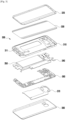
- the electronic device 300 includes a lateral bezel structure 310, may include a first support member 311 (e.g., a bracket), includes a front plate 320, may include a display 330 (e.g., the display 101), a printed circuit board (PCB) 340, a battery 350, a second support member 360 (e.g., a rear case), an antenna 370, and includes a rear plate 380.
- the electronic device 300 may omit at least one (e.g., the first support member 311 or the second support member 360) of the above components or may further include another component.
- Some components of the electronic device 300 may be the same as or similar to those of the electronic device 100 shown in FIG. 1 or FIG. 2 , thus, descriptions thereof are omitted below.
- the first support member 311 is disposed inside the electronic device 300 and may be connected to, or integrated with, the lateral bezel structure 310.
- the first support member 311 may be formed of, for example, a metallic material and/or a non-metal (e.g., polymer) material.
- the first support member 311 may be combined with the display 330 at one side thereof and also combined with the PCB 340 at the other side thereof.
- a processor, a memory, and/or an interface may be mounted on the PCB 340.
- the processor may include, for example, one or more of a central processing unit (CPU), an application processor (AP), a graphics processing unit (GPU), an image signal processor (ISP), a sensor hub processor, or a communications processor (CP).
- CPU central processing unit
- AP application processor
- GPU graphics processing unit
- ISP image signal processor
- sensor hub processor or a communications processor (CP).
- CP communications processor
- the memory may include, for example, volatile memory or non-volatile memory.
- the interface may include, for example, a high definition multimedia interface (HDMI), a USB interface, a secure digital (SD) card interface, and/or an audio interface.
- HDMI high definition multimedia interface
- USB USB interface
- SD secure digital
- audio audio interface
- the interface may electrically or physically connect the electronic device 300 with an external electronic device and may include a USB connector, an SD card/multimedia card (MMC) connector, or an audio connector.
- MMC multimedia card
- the battery 350 is a device for supplying power to at least one component of the electronic device 300, and may include, for example, a non-rechargeable primary battery, a rechargeable secondary battery, or a fuel cell. At least a part of the battery 350 may be disposed on substantially the same plane as the PCB 340. The battery 350 may be integrally disposed within the electronic device 300, and may be detachably disposed from the electronic device 300.
- the antenna 370 may be disposed between the rear plate 380 and the battery 350.
- the antenna 370 may include, for example, a near field communication (NFC) antenna, a wireless charging antenna, and/or a magnetic secure transmission (MST) antenna.
- NFC near field communication
- MST magnetic secure transmission
- the antenna 370 may perform short-range communication with an external device, or transmit and receive power required for charging wirelessly.
- An antenna structure may be formed by a part or combination of the lateral bezel structure 310 and/or the first support member 311.
- FIGS. 4A and 4B illustrate cross-sectional views schematically showing a decoration film 400 according to an embodiment of the disclosure.
- the decoration film 400 includes an adhesive layer 410, a first decoration layer 420, and a second decoration layer 430.
- the adhesive layer 410 may be combined with an inner surface of the front plate or rear plate of the electronic device.
- the inner surface of the front plate or rear plate may refer to a surface facing an inner space in which various components of the electronic device are disposed.
- the adhesive layer 410 may be formed of, for example, a pressure sensitive adhesive (PSA) or an optical clear adhesive (OCA).
- PSA pressure sensitive adhesive
- OCA optical clear adhesive
- the adhesive layer 410 may include a processible layer (e.g., a primer layer).
- the first decoration layer 420 includes a first shape-cured layer 421 and a first color layer 423.
- the first shape-cured layer 421 may be formed by applying a polymer resin in a fluid state to a mold having a first three-dimensional pattern and then curing the applied polymer resin by an external stimulus such as ultraviolet rays.
- the first shape-cured layer 421 may be formed using a polymer resin composition of acrylic, urethane, or silicone.
- the first shape-cured layer 421 is combined with the adhesive layer 410.
- the first shape-cured layer 421 may have the first three-dimensional pattern distributed over the entire or partial area of the front plate or rear plate.
- the first shape-cured layer 421 may reflect light in various directions through the first three-dimensional pattern to offer variations in a pattern recognizable to the user.
- the first three-dimensional pattern may be composed of linear zones repeatedly arranged and gradually changing in size from one end to the other end as shown in FIG. 6A or from a central portion to both ends as shown in FIG. 6B .
- the first three-dimensional pattern may be composed of many circles or polygons repeatedly arranged and gradually changed in size.
- the first three-dimensional pattern may be composed of a plurality of repeated pyramid-shaped regions.
- the first color layer 423 may be formed on the first shape-cured layer 421 in various colors.
- the first color layer 423 may be formed through deposition of a metal or an oxide. For example, depositing a metal such as indium or an oxide such as titanium oxide, silicon oxide, or aluminum oxide on the first shape-cured layer 421 may result in forming the first color layer 423 having a specific color.
- the second decoration layer 430 includes a second shape-cured layer 431 and a second color layer 433.
- the second shape-cured layer 431 may be formed by applying a polymer resin in a fluid state to a mold having a second three-dimensional pattern and then curing the applied polymer resin by an external stimulus such as ultraviolet rays. Curing process may be performed simultaneously for the first and second shape-cured layers 421 and 431.
- the second shape-cured layer 431 may be combined with the first color layer 423.
- the second shape-cured layer 431 may have the second three-dimensional pattern distributed over the entire or partial area of the front plate or rear plate.
- the second shape-cured layer 431 may reflect light in various directions through the second three-dimensional pattern to offer variations in a pattern recognizable to the user.
- the second three-dimensional pattern may be formed of various patterns as shown in FIGS. 6A to 6F .
- the second color layer 433 may be formed on the second shape-cured layer 431 in various colors. Like the first color layer 423, the second color layer 433 as well may be formed through deposition of a metal or an oxide. For example, depositing a metal such as indium or an oxide such as titanium oxide, silicon oxide, or aluminum oxide on the second shape-cured layer 431 may result in forming the second color layer 433 having a specific color.
- the first three-dimensional pattern and the second three-dimensional pattern may be identical or similar to each other as shown in FIG. 4A , but according to the presently claimed invention they are different from each other as shown/illustrated in FIG. 4B .
- the first color layer 423 and the second color layer 433 may be formed in identical or similar colors or in completely different colors.
- first and second three-dimensional patterns are identical or similar to each other, the shape of the corresponding pattern may be realized clearer and remarkably.
- a combination of both patterns may create a new three-dimensional pattern.
- FIG. 4B the first and second three-dimensional patterns are illustrated simply with focus on being different. However, a great variety of combinations in different patterns may be used as shown in FIGS. 6A to 6F .
- the color(s) may be realized clearer and remarkably by the second shape-cured layer 431 interposed between the first and second color layers 423 and 433.
- the first color layer 423 and the second color layer 433 are formed in different colors, the first color, the second color, or any new color resulting from a combination of the first and second colors may be seen to the user, depending on a direction viewed by the user.
- the decoration film 400 may further include a surface treatment layer 450 interposed between the first color layer 423 of the first decoration layer 420 and the second shape-cured layer 431 of the second decoration layer 430.
- the surface treatment layer 450 improves the binding strength between the first and second decoration layers 420 and 430 and may be formed by processing a surface of any one of the first color layer 423 or the second shape-cured layer 431.
- a treatment for increasing the surface energy through, for example, a plasma treatment or an etching treatment may be performed.
- the decoration film 400 may further include a shielding printed layer 440 formed on the second color layer 433.
- the shielding printed layer 440 may not only provide a flat surface onto an uneven surface of the second shape-cured layer 431, but also block various components inside the electronic device from being viewed outside.
- the decoration film 400 may use much more decoration layers overlapped with each other.
- FIGS. 5A and 5B illustrate cross-sectional views schematically showing a decoration film 500 according to an embodiment of the disclosure.
- the decoration film 500 includes an adhesive layer 510, a base film 560, a first decoration layer 520, and a second decoration layer 530.
- the adhesive layer 510 may be combined with an inner surface of the front plate or rear plate of the electronic device.
- the adhesive layer 510 may be formed of, for example, a PSA or an OCA.
- the adhesive layer 510 may be in the form of an adhesive tape applied to one surface of the base film 560, and the first decoration layer 520 may be formed on the other surface of the base film 560.
- the first decoration layer 520 includes a first shape-cured layer 521 and a first color layer 523.
- the first shape-cured layer 521 may be formed by applying a polymer resin in a fluid state to a mold having a first three-dimensional pattern and then curing the applied polymer resin by an external stimulus such as ultraviolet rays.
- the first shape-cured layer 521 may be formed using a polymer resin composition of acrylic, urethane, or silicone.
- the first shape-cured layer 521 may be combined with the other surface of the base film 560.
- the first shape-cured layer 521 may have the first three-dimensional pattern distributed over the entire or partial area of the front plate or rear plate.
- the first shape-cured layer 521 may reflect light in various directions through the first three-dimensional pattern to offer variations in a pattern recognizable to the user.
- the first three-dimensional pattern may be composed of linear zones repeatedly arranged and gradually changing in size from one end to the other end as shown in FIG. 6A or from a central portion to both ends as shown in FIG. 6B .
- the first three-dimensional pattern may be composed of many circles or polygons repeatedly arranged and gradually changed in size.
- the first three-dimensional pattern may be composed of a plurality of repeated pyramid-shaped regions.
- the first color layer 523 may be formed on the first shape-cured layer 521 in various colors.
- the first color layer 523 may be formed through deposition of a metal or an oxide. For example, depositing a metal such as indium or an oxide such as titanium oxide, silicon oxide, or aluminum oxide on the first shape-cured layer 521 may result in forming the first color layer 523 having a specific color.
- the second decoration layer 530 includes a second shape-cured layer 531 and a second color layer 533.
- the second shape-cured layer 531 may be formed by applying a polymer resin in a fluid state to a mold having a second three-dimensional pattern and then curing the applied polymer resin by an external stimulus such as ultraviolet rays. Curing process may be performed simultaneously for the first and second shape-cured layers 521 and 531.
- the second shape-cured layer 531 may be combined with the first color layer 523.
- the second shape-cured layer 531 may have the second three-dimensional pattern distributed over the entire or partial area of the front plate or rear plate.
- the second shape-cured layer 531 may reflect light in various directions through the second three-dimensional pattern to offer variations in a pattern recognizable to the user.
- the second three-dimensional pattern may be formed of various patterns as shown in FIGS. 6A to 6F .
- the second color layer 533 may be formed on the second shape-cured layer 531 in various colors. Like the first color layer 523, the second color layer 533 as well may be formed through deposition of a metal or an oxide. For example, depositing a metal such as indium or an oxide such as titanium oxide, silicon oxide, or aluminum oxide on the second shape-cured layer 531 may result in forming the second color layer 533 having a specific color.
- the first three-dimensional pattern and the second three-dimensional pattern may be identical or similar to each other as shown in FIG. 5A , but according to the presently claimed invention they are different from each other as shown/illustrated in FIG. 5B .
- the first color layer 523 and the second color layer 533 may be formed in identical or similar colors or in completely different colors.
- the decoration film 500 may further include a shielding printed layer 540 formed on the second color layer 533.
- FIGS. 6A to 6F illustrate views showing three-dimensional patterns of a decoration film according to various embodiments of the disclosure.
- the three-dimensional pattern may be provided to each decoration layer (especially, a shape-cured layer) and distributed over the entire or partial area of the front plate or rear plate of the electronic device.
- the three-dimensional patterns provided to the respective decoration layers may be identical or similar to each other or different from each other.
- Each three-dimensional pattern may be composed of linear zones repeatedly arranged and gradually changing in size from one end to the other end as shown in FIG. 6A or from a central portion to both ends as shown in FIG. 6B .
- each three-dimensional pattern may be composed of many circles or polygons repeatedly arranged and gradually changed in size.
- each three-dimensional pattern may be composed of a plurality of repeated pyramid-shaped regions.
- FIG. 7 illustrates a flow diagram illustrating a method of manufacturing a decoration film according to an embodiment of the disclosure.
- the front plate or rear plate of the electronic device may be, for example, a reinforced glass fabricated through a shape machining operation 711 and a reinforcement operation 713.
- any other material, such as plastic, that allows the decoration film to be combined may be used for the front plate or the rear plate.
- the first decoration layer may be formed through an operation 721 of curing the first shape-cured layer by ultraviolet rays and an operation 723 of depositing the first color layer. Then, a surface treatment operation 750 may be performed on the first color layer of the first decoration layer.
- the second decoration layer may be formed through an operation 731 of curing the second shape-cured layer by ultraviolet rays and an operation 733 of depositing the second color layer. Then, a shield printing operation 740 may be performed on the second color layer.
- the decoration film according to an embodiment may be completed.
- the decoration film may be combined with the front plate or the back plate through a lamination operation.
- the electronic device including the decoration film according to an embodiment of the disclosure can be obtained.
- a decoration film includes an adhesive layer, a first decoration layer, and a second decoration layer.
- the adhesive layer may be combined with one of a front plate and a rear plate of an electronic device.
- the first decoration layer includes a first shape-cured layer and a first color layer, wherein the first shape-cured layer is combined with the adhesive layer, has a first three-dimensional pattern, and is cured by an external stimulus, and wherein the first color layer is combined with the first shape-cured layer and has a first color.
- the second decoration layer includes a second shape-cured layer and a second color layer, wherein the second shape-cured layer is combined with the first color layer, has a second three-dimensional pattern, and is cured by an external stimulus, and wherein the second color layer is combined with the second shape-cured layer and has a second color.
- the decoration film may further include a shielding printed layer formed on the second color layer of the second decoration layer.
- At least one of the first color layer and the second color layer may be formed through deposition of a metal or an oxide.
- the first color of the first color layer and the second color of the second color layer may be different from each other.
- the decoration film may further include a surface treatment layer interposed between the first color layer and the second shape-cured layer to improve a binding strength between the first color layer and the second shape-cured layer.
- At least one of the first shape-cured layer and the second shape-cured layer may be formed by applying a polymer resin and curing the applied polymer resin by ultraviolet rays.
- the first three-dimensional pattern of the first shape-cured layer and the second three-dimensional pattern of the second shape-cured layer are different from each other.
- the decoration film may further include a base film interposed between the adhesive layer and the first shape-cured layer.
- an electronic device may include a housing, a display, an adhesive layer, a first decoration layer, and a second decoration layer.
- the housing may include a front plate facing a first direction, a rear plate facing a second direction opposite to the first direction, and a lateral member surrounding a space between the front plate and the rear plate.
- the display may be viewed through at least a portion of the front plate.
- the adhesive layer may be combined with one of the front plate and the rear plate.
- the first decoration layer may include a first shape-cured layer and a first color layer, wherein the first shape-cured layer is combined with the adhesive layer, has a first three-dimensional pattern, and is cured by an external stimulus, and wherein the first color layer is combined with the first shape-cured layer and has a first color.
- the second decoration layer may include a second shape-cured layer and a second color layer, wherein the second shape-cured layer is combined with the first color layer, has a second three-dimensional pattern, and is cured by an external stimulus, and wherein the second color layer is combined with the second shape-cured layer and has a second color.
- the electronic device may further include a shielding printed layer formed on the second color layer of the second decoration layer.
- At least one of the first color layer and the second color layer may be formed through deposition of a metal or an oxide.
- the first color of the first color layer and the second color of the second color layer may be different from each other.
- the electronic device may further include a surface treatment layer interposed between the first color layer and the second shape-cured layer to improve a binding strength between the first color layer and the second shape-cured layer.
- At least one of the first shape-cured layer and the second shape-cured layer may be formed by applying a polymer resin and curing the applied polymer resin by ultraviolet rays.
- the first three-dimensional pattern of the first shape-cured layer and the second three-dimensional pattern of the second shape-cured layer are different from each other.
- the electronic device may further include a base film interposed between the adhesive layer and the first shape-cured layer.
Landscapes
- Engineering & Computer Science (AREA)
- Mechanical Engineering (AREA)
- Laminated Bodies (AREA)
- Casings For Electric Apparatus (AREA)
Description
- The disclosure relates to a decoration film and an electronic device including the decoration film.
- With the growths of related technologies, electronic devices such as a smart phone have been developed to have a thin thickness, a reduced weight, a high performance, and various functions so as to improve portability and usability. In addition, recent electronic devices have beautiful exterior designs so as to appeal to consumers.
- Meanwhile, in applying various design elements to a case surface of an electronic device, many studies on how to improve beauty and robustness are being conducted.
-
US 2018/249586 A1 describes a planar exterior surface mounting member, formed by an anti-scratch hard coating layer, a transparent polymer base layer, a UV molding layer, PVD (Physical Vapor Deposition) color layer and a shield layer. The UV molding layer may be formed of a plurality of molding layers. -
US 2014/118903 A1 describes casings for electronic devices where the case frame has a multilayer structure comprising oxide deposited layers and a first and second painting layer. -
US 2014/113089 A1 describes housings for electronic devices that comprises a substrate and three color layers, as well as two metallic coatings and a protection layer. -
KR 2017 0107756 A - Various embodiments of the disclosure provide a decoration film used for a case surface of an electronic device. The decoration film may have various patterns and colors, which can be variously and changeably recognized according to a viewing angle.
- The invention is set out in the appended set of claims.
- Before undertaking the [Mode for Invention] below, it may be advantageous to set forth definitions of certain words and phrases used throughout this patent document: the terms "include" and "comprise," as well as derivatives thereof, mean inclusion without limitation; the term "or," is inclusive, meaning and/or; the phrases "associated with" and "associated therewith," as well as derivatives thereof, may mean to include, be included within, interconnect with, contain, be contained within, connect to or with, couple to or with, be communicable with, cooperate with, interleave, juxtapose, be proximate to, be bound to or with, have, have a property of, or the like; and the term "controller" means any device, system or part thereof that controls at least one operation, such a device may be implemented in hardware, firmware or software, or some combination of at least two of the same. It should be noted that the functionality associated with any particular controller may be centralized or distributed, whether locally or remotely.
- Moreover, various functions described below can be implemented or supported by one or more computer programs, each of which is formed from computer readable program code and embodied in a computer readable medium. The terms "application" and "program" refer to one or more computer programs, software components, sets of instructions, procedures, functions, objects, classes, instances, related data, or a portion thereof adapted for implementation in a suitable computer readable program code. The phrase "computer readable program code" includes any type of computer code, including source code, object code, and executable code. The phrase "computer readable medium" includes any type of medium capable of being accessed by a computer, such as read only memory (ROM), random access memory (RAM), a hard disk drive, a compact disc (CD), a digital video disc (DVD), or any other type of memory. A "non-transitory" computer readable medium excludes wired, wireless, optical, or other communication links that transport transitory electrical or other signals. A non-transitory computer readable medium includes media where data can be permanently stored and media where data can be stored and later overwritten, such as a rewritable optical disc or an erasable memory device.
- Definitions for certain words and phrases are provided throughout this patent document, those of ordinary skill in the art should understand that in many, if not most instances, such definitions apply to prior, as well as future uses of such defined words and phrases.
- According to various embodiments of the disclosure, the decoration film may include a plurality of decoration layers have various patterns and colors. Depending on a viewing angle, such patterns may be recognized as various new patterns in combination. Similarly, depending on a viewing angle, such colors may be recognized as various new colors in combination.
- The above and other aspects, features and advantages of certain embodiments of the disclosure will be more apparent from the following detailed description, taken in conjunction with the accompanying drawings.
-
FIG. 1 illustrates a perspective view showing a front surface of an electronic device according to an embodiment. -
FIG. 2 illustrates a perspective view showing a rear surface of the electronic device shown inFIG. 1 . -
FIG. 3 illustrates an exploded perspective view showing the electronic device shown inFIGS. 1 and 2 . -
FIGS. 4A and 4B illustrate cross-sectional views schematically showing a decoration film according to an embodiment of the disclosure. -
FIGS. 5A and5B illustrate cross-sectional views schematically showing a decoration film according to an embodiment of the disclosure. -
FIGS. 6A to 6F illustrate views showing three-dimensional patterns of a decoration film according to various embodiments of the disclosure. -
FIG. 7 illustrates a flow diagram illustrating a method of manufacturing a decoration film according to an embodiment of the disclosure. -
FIGS. 1 through 7 , discussed below, and the various embodiments used to describe the principles of the present disclosure in this patent document are by way of illustration only and should not be construed in any way to limit the scope of the disclosure. Those skilled in the art will understand that the principles of the present disclosure may be implemented in any suitably arranged system or device. - Hereinafter, embodiments of the disclosure will be described in detail with reference to accompanying drawings.
- Referring to
FIGS. 1 and 2 , according to an embodiment, anelectronic device 100 includes ahousing 110 that includes a first surface (or front surface) 110A, a second surface (or rear surface) 110B, and alateral surface 110C that surrounds a space between thefirst surface 110A and thesecond surface 110B. According to an embodiment, thehousing 110 may refer to a structure that forms a part of thefirst surface 110A, thesecond surface 110B, and thelateral surface 110C. According to an embodiment, thefirst surface 110A may be formed of a front plate 102 (e.g., a glass plate or polymer plate coated with a variety of coating layers) at least a part of which is substantially transparent. Thesecond surface 110B may be formed of arear plate 111 which is substantially opaque. Therear plate 111 may be formed of, for example, coated or colored glass, ceramic, polymer, metal (e.g., aluminum, stainless steel (STS), or magnesium), or any combination thereof. Thelateral surface 110C may be formed of a lateral bezel structure (or "lateral member") 118 which is combined with thefront plate 102 and therear plate 111 and includes a metal and/or polymer. Therear plate 111 and thelateral bezel structure 118 may be integrally formed and may be of the same material (e.g., a metallic material such as aluminum). - In the shown embodiment, the
front plate 102 may include twofirst regions 110D disposed at long edges thereof, respectively, and bent and extended seamlessly from thefirst surface 110A toward therear plate 111. In the shown embodiment, therear plate 111 may include twosecond regions 110E disposed at long edges thereof, respectively, and bent and extended seamlessly from thesecond surface 110B toward the front plate 102 (refer toFIG. 2 ). In various embodiments, the front plate 102 (or the rear plate 111) may include only one of thefirst regions 110D (or of thesecond regions 110E). In various embodiments, thefirst regions 110D or thesecond regions 110E may be omitted in part. In the embodiments, when viewed from a lateral side of theelectronic device 100, thelateral bezel structure 118 may have a first thickness (or width) on a lateral side where thefirst region 110D or thesecond region 110E is not included, and may have a second thickness, being less than the first thickness, on another lateral side where thefirst region 110D or thesecond region 110E is included. - According to an embodiment, the
electronic device 100 may include at least one of adisplay 101,audio modules sensor modules camera modules key input devices 117, alight emitting device 106, andconnector holes electronic device 100 may omit at least one (e.g., thekey input devices 117 or the light emitting device 106) of the above components, or may further include other components. - The
display 101 may be exposed through a substantial portion of thefront plate 102, for example. In various embodiments, at least a part of thedisplay 101 may be exposed through thefront plate 102 that forms thefirst surface 110A and thefirst region 110D of thelateral surface 110C. In various embodiments, outlines (i.e., edges and corners) of thedisplay 101 may have substantially the same form as those of thefront plate 102. In an embodiment, the spacing between the outline of thedisplay 101 and the outline of thefront plate 102 may be substantially unchanged in order to enlarge the exposed area of thedisplay 101. - In an embodiment, a recess or opening may be formed in a portion of a display area of the
display 101 to accommodate at least one of theaudio module 114, thesensor module 104, thecamera module 105, and thelight emitting device 106. In an embodiment, at least one of theaudio module 114, thesensor module 104, thecamera module 105, thefingerprint sensor 116, and thelight emitting element 106 may be disposed on the back of the display area of thedisplay 101. In an embodiment, thedisplay 101 may be combined with, or adjacent to, a touch sensing circuit, a pressure sensor capable of measuring the touch strength (pressure), and/or a digitizer for detecting a stylus pen. In various embodiments, at least a part of thesensor modules key input devices 117 may be disposed in thefirst region 110D and/or thesecond region 110E. - The
audio modules microphone hole 103 and speaker holes 107 and 114, respectively. Themicrophone hole 103 may contain a microphone disposed therein for acquiring external sounds and, in a case, contain a plurality of microphones to sense a sound direction. The speaker holes 107 and 114 may be classified into anexternal speaker hole 107 and acall receiver hole 114. In various embodiments, themicrophone hole 103 and the speaker holes 107 and 114 may be implemented as a single hole, or a speaker (e.g., a piezo speaker) may be provided without the speaker holes 107 and 114. - The
sensor modules electronic device 100 or to an external environmental condition. Thesensor modules first surface 110A of thehousing 110, and/or a third sensor module 119 (e.g., a heart rate monitor (HRM) sensor) and/or a fourth sensor module 116 (e.g., a fingerprint sensor) disposed on thesecond surface 110B of thehousing 110. The fingerprint sensor may be disposed on thesecond surface 110B as well as thefirst surface 110A (e.g., the display 101) of thehousing 110. Theelectronic device 100 may further include at least one of a gesture sensor, a gyro sensor, an air pressure sensor, a magnetic sensor, an acceleration sensor, a grip sensor, a color sensor, an infrared (IR) sensor, a biometric sensor, a temperature sensor, a humidity sensor, or an illuminance sensor. - The
camera modules first camera device 105 disposed on thefirst surface 110A of theelectronic device 100, and asecond camera device 112 and/or aflash 113 disposed on thesecond surface 110B. Thecamera module 105 or thecamera module 112 may include one or more lenses, an image sensor, and/or an image signal processor. Theflash 113 may include, for example, a light emitting diode or a xenon lamp. In various embodiments, two or more lenses (infrared cameras, wide angle and telephoto lenses) and image sensors may be disposed on one side of theelectronic device 100. - The
key input devices 117 may be disposed on thelateral surface 110C of thehousing 110. In an embodiment, theelectronic device 100 may not include some or all of thekey input devices 117 described above, and thekey input devices 117 which are not included may be implemented in another form such as a soft key on thedisplay 101. In various embodiments, thekey input devices 117 may include thesensor module 116 disposed on thesecond surface 110B of thehousing 110. - The
light emitting device 106 may be disposed on thefirst surface 110A of thehousing 110, for example. For example, thelight emitting device 106 may provide status information of theelectronic device 100 in an optical form. In various embodiments, thelight emitting device 106 may provide a light source associated with the operation of thecamera module 105. Thelight emitting device 106 may include, for example, a light emitting diode (LED), an IR LED, or a xenon lamp. - The connector holes 108 and 109 may include a
first connector hole 108 adapted for a connector (e.g., a universal serial bus (USB) connector) for transmitting and receiving power and/or data to and from an external electronic device, and/or asecond connector hole 109 adapted for a connector (e.g., an earphone jack) for transmitting and receiving an audio signal to and from an external electronic device. - Referring to
FIG. 3 , theelectronic device 300 includes alateral bezel structure 310, may include a first support member 311 (e.g., a bracket), includes afront plate 320, may include a display 330 (e.g., the display 101), a printed circuit board (PCB) 340, abattery 350, a second support member 360 (e.g., a rear case), anantenna 370, and includes arear plate 380. In various embodiment, theelectronic device 300 may omit at least one (e.g., thefirst support member 311 or the second support member 360) of the above components or may further include another component. Some components of theelectronic device 300 may be the same as or similar to those of theelectronic device 100 shown inFIG. 1 or FIG. 2 , thus, descriptions thereof are omitted below. - The
first support member 311 is disposed inside theelectronic device 300 and may be connected to, or integrated with, thelateral bezel structure 310. Thefirst support member 311 may be formed of, for example, a metallic material and/or a non-metal (e.g., polymer) material. Thefirst support member 311 may be combined with thedisplay 330 at one side thereof and also combined with thePCB 340 at the other side thereof. On thePCB 340, a processor, a memory, and/or an interface may be mounted. The processor may include, for example, one or more of a central processing unit (CPU), an application processor (AP), a graphics processing unit (GPU), an image signal processor (ISP), a sensor hub processor, or a communications processor (CP). - The memory may include, for example, volatile memory or non-volatile memory.
- The interface may include, for example, a high definition multimedia interface (HDMI), a USB interface, a secure digital (SD) card interface, and/or an audio interface. The interface may electrically or physically connect the
electronic device 300 with an external electronic device and may include a USB connector, an SD card/multimedia card (MMC) connector, or an audio connector. - The
battery 350 is a device for supplying power to at least one component of theelectronic device 300, and may include, for example, a non-rechargeable primary battery, a rechargeable secondary battery, or a fuel cell. At least a part of thebattery 350 may be disposed on substantially the same plane as thePCB 340. Thebattery 350 may be integrally disposed within theelectronic device 300, and may be detachably disposed from theelectronic device 300. - The
antenna 370 may be disposed between therear plate 380 and thebattery 350. Theantenna 370 may include, for example, a near field communication (NFC) antenna, a wireless charging antenna, and/or a magnetic secure transmission (MST) antenna. Theantenna 370 may perform short-range communication with an external device, or transmit and receive power required for charging wirelessly. An antenna structure may be formed by a part or combination of thelateral bezel structure 310 and/or thefirst support member 311. -
FIGS. 4A and 4B illustrate cross-sectional views schematically showing adecoration film 400 according to an embodiment of the disclosure. - The
decoration film 400 according to an embodiment includes anadhesive layer 410, afirst decoration layer 420, and asecond decoration layer 430. - The
adhesive layer 410 according to an embodiment may be combined with an inner surface of the front plate or rear plate of the electronic device. The inner surface of the front plate or rear plate may refer to a surface facing an inner space in which various components of the electronic device are disposed. Theadhesive layer 410 may be formed of, for example, a pressure sensitive adhesive (PSA) or an optical clear adhesive (OCA). Theadhesive layer 410 may include a processible layer (e.g., a primer layer). - The
first decoration layer 420 according to an embodiment includes a first shape-curedlayer 421 and afirst color layer 423. - The first shape-cured
layer 421 according to an embodiment may be formed by applying a polymer resin in a fluid state to a mold having a first three-dimensional pattern and then curing the applied polymer resin by an external stimulus such as ultraviolet rays. For example, the first shape-curedlayer 421 may be formed using a polymer resin composition of acrylic, urethane, or silicone. The first shape-curedlayer 421 is combined with theadhesive layer 410. The first shape-curedlayer 421 may have the first three-dimensional pattern distributed over the entire or partial area of the front plate or rear plate. The first shape-curedlayer 421 may reflect light in various directions through the first three-dimensional pattern to offer variations in a pattern recognizable to the user. For example, the first three-dimensional pattern may be composed of linear zones repeatedly arranged and gradually changing in size from one end to the other end as shown inFIG. 6A or from a central portion to both ends as shown inFIG. 6B . Alternatively, as shown inFIGS. 6C to 6E , the first three-dimensional pattern may be composed of many circles or polygons repeatedly arranged and gradually changed in size. Alternatively, as shown inFIG. 6F , the first three-dimensional pattern may be composed of a plurality of repeated pyramid-shaped regions. - The
first color layer 423 according to an embodiment may be formed on the first shape-curedlayer 421 in various colors. Thefirst color layer 423 may be formed through deposition of a metal or an oxide. For example, depositing a metal such as indium or an oxide such as titanium oxide, silicon oxide, or aluminum oxide on the first shape-curedlayer 421 may result in forming thefirst color layer 423 having a specific color. - The
second decoration layer 430 according to an embodiment includes a second shape-curedlayer 431 and asecond color layer 433. - The second shape-cured
layer 431 according to an embodiment may be formed by applying a polymer resin in a fluid state to a mold having a second three-dimensional pattern and then curing the applied polymer resin by an external stimulus such as ultraviolet rays. Curing process may be performed simultaneously for the first and second shape-curedlayers layer 431 may be combined with thefirst color layer 423. Like the first shape-curedlayer 421, the second shape-curedlayer 431 may have the second three-dimensional pattern distributed over the entire or partial area of the front plate or rear plate. The second shape-curedlayer 431 may reflect light in various directions through the second three-dimensional pattern to offer variations in a pattern recognizable to the user. Like the first three-dimensional pattern, the second three-dimensional pattern may be formed of various patterns as shown inFIGS. 6A to 6F . - The
second color layer 433 according to an embodiment may be formed on the second shape-curedlayer 431 in various colors. Like thefirst color layer 423, thesecond color layer 433 as well may be formed through deposition of a metal or an oxide. For example, depositing a metal such as indium or an oxide such as titanium oxide, silicon oxide, or aluminum oxide on the second shape-curedlayer 431 may result in forming thesecond color layer 433 having a specific color. - The first three-dimensional pattern and the second three-dimensional pattern may be identical or similar to each other as shown in
FIG. 4A , but according to the presently claimed invention they are different from each other as shown/illustrated inFIG. 4B . In addition, thefirst color layer 423 and thesecond color layer 433 may be formed in identical or similar colors or in completely different colors. - When the first and second three-dimensional patterns are identical or similar to each other, the shape of the corresponding pattern may be realized clearer and remarkably. When the first and second three-dimensional patterns are different from each other, a combination of both patterns may create a new three-dimensional pattern. In
FIG. 4B , the first and second three-dimensional patterns are illustrated simply with focus on being different. However, a great variety of combinations in different patterns may be used as shown inFIGS. 6A to 6F . - When the
first color layer 423 and thesecond color layer 433 are formed in identical or similar colors, the color(s) may be realized clearer and remarkably by the second shape-curedlayer 431 interposed between the first and second color layers 423 and 433. When thefirst color layer 423 and thesecond color layer 433 are formed in different colors, the first color, the second color, or any new color resulting from a combination of the first and second colors may be seen to the user, depending on a direction viewed by the user. - Meanwhile, according an embodiment, the
decoration film 400 may further include asurface treatment layer 450 interposed between thefirst color layer 423 of thefirst decoration layer 420 and the second shape-curedlayer 431 of thesecond decoration layer 430. Thesurface treatment layer 450 improves the binding strength between the first and second decoration layers 420 and 430 and may be formed by processing a surface of any one of thefirst color layer 423 or the second shape-curedlayer 431. To improve the binding strength, a treatment for increasing the surface energy through, for example, a plasma treatment or an etching treatment may be performed. - In addition, according an embodiment, the
decoration film 400 may further include a shielding printedlayer 440 formed on thesecond color layer 433. The shielding printedlayer 440 may not only provide a flat surface onto an uneven surface of the second shape-curedlayer 431, but also block various components inside the electronic device from being viewed outside. - Although the above description has used the first and second decoration layers 420 and 430, there are various embodiments. In various embodiments, the
decoration film 400 may use much more decoration layers overlapped with each other. -
FIGS. 5A and5B illustrate cross-sectional views schematically showing adecoration film 500 according to an embodiment of the disclosure. - The
decoration film 500 according to an embodiment includes anadhesive layer 510, abase film 560, afirst decoration layer 520, and asecond decoration layer 530. - The
adhesive layer 510 according to an embodiment may be combined with an inner surface of the front plate or rear plate of the electronic device. Theadhesive layer 510 may be formed of, for example, a PSA or an OCA. Theadhesive layer 510 may be in the form of an adhesive tape applied to one surface of thebase film 560, and thefirst decoration layer 520 may be formed on the other surface of thebase film 560. - The
first decoration layer 520 according to an embodiment includes a first shape-curedlayer 521 and afirst color layer 523. - The first shape-cured
layer 521 according to an embodiment may be formed by applying a polymer resin in a fluid state to a mold having a first three-dimensional pattern and then curing the applied polymer resin by an external stimulus such as ultraviolet rays. For example, the first shape-curedlayer 521 may be formed using a polymer resin composition of acrylic, urethane, or silicone. The first shape-curedlayer 521 may be combined with the other surface of thebase film 560. The first shape-curedlayer 521 may have the first three-dimensional pattern distributed over the entire or partial area of the front plate or rear plate. The first shape-curedlayer 521 may reflect light in various directions through the first three-dimensional pattern to offer variations in a pattern recognizable to the user. For example, the first three-dimensional pattern may be composed of linear zones repeatedly arranged and gradually changing in size from one end to the other end as shown inFIG. 6A or from a central portion to both ends as shown inFIG. 6B . Alternatively, as shown inFIGS. 6C to 6E , the first three-dimensional pattern may be composed of many circles or polygons repeatedly arranged and gradually changed in size. Alternatively, as shown inFIG. 6F , the first three-dimensional pattern may be composed of a plurality of repeated pyramid-shaped regions. - The
first color layer 523 according to an embodiment may be formed on the first shape-curedlayer 521 in various colors. Thefirst color layer 523 may be formed through deposition of a metal or an oxide. For example, depositing a metal such as indium or an oxide such as titanium oxide, silicon oxide, or aluminum oxide on the first shape-curedlayer 521 may result in forming thefirst color layer 523 having a specific color. - The
second decoration layer 530 according to an embodiment includes a second shape-curedlayer 531 and asecond color layer 533. - The second shape-cured
layer 531 according to an embodiment may be formed by applying a polymer resin in a fluid state to a mold having a second three-dimensional pattern and then curing the applied polymer resin by an external stimulus such as ultraviolet rays. Curing process may be performed simultaneously for the first and second shape-curedlayers layer 531 may be combined with thefirst color layer 523. Like the first shape-curedlayer 521, the second shape-curedlayer 531 may have the second three-dimensional pattern distributed over the entire or partial area of the front plate or rear plate. The second shape-curedlayer 531 may reflect light in various directions through the second three-dimensional pattern to offer variations in a pattern recognizable to the user. Like the first three-dimensional pattern, the second three-dimensional pattern may be formed of various patterns as shown inFIGS. 6A to 6F . - The
second color layer 533 according to an embodiment may be formed on the second shape-curedlayer 531 in various colors. Like thefirst color layer 523, thesecond color layer 533 as well may be formed through deposition of a metal or an oxide. For example, depositing a metal such as indium or an oxide such as titanium oxide, silicon oxide, or aluminum oxide on the second shape-curedlayer 531 may result in forming thesecond color layer 533 having a specific color. - The first three-dimensional pattern and the second three-dimensional pattern may be identical or similar to each other as shown in
FIG. 5A , but according to the presently claimed invention they are different from each other as shown/illustrated inFIG. 5B . In addition, thefirst color layer 523 and thesecond color layer 533 may be formed in identical or similar colors or in completely different colors. - Meanwhile, according an embodiment, the
decoration film 500 may further include a shielding printedlayer 540 formed on thesecond color layer 533. -
FIGS. 6A to 6F illustrate views showing three-dimensional patterns of a decoration film according to various embodiments of the disclosure. - As described above, the three-dimensional pattern may be provided to each decoration layer (especially, a shape-cured layer) and distributed over the entire or partial area of the front plate or rear plate of the electronic device. In addition, the three-dimensional patterns provided to the respective decoration layers may be identical or similar to each other or different from each other.
- Each three-dimensional pattern may be composed of linear zones repeatedly arranged and gradually changing in size from one end to the other end as shown in
FIG. 6A or from a central portion to both ends as shown inFIG. 6B . Alternatively, as shown inFIGS. 6C to 6E , each three-dimensional pattern may be composed of many circles or polygons repeatedly arranged and gradually changed in size. Alternatively, as shown inFIG. 6F , each three-dimensional pattern may be composed of a plurality of repeated pyramid-shaped regions. -
FIG. 7 illustrates a flow diagram illustrating a method of manufacturing a decoration film according to an embodiment of the disclosure. - According to an embodiment, the front plate or rear plate of the electronic device may be, for example, a reinforced glass fabricated through a
shape machining operation 711 and areinforcement operation 713. Alternatively, any other material, such as plastic, that allows the decoration film to be combined may be used for the front plate or the rear plate. - According to an embodiment, in order to fabricate the decoration film, the first decoration layer may be formed through an
operation 721 of curing the first shape-cured layer by ultraviolet rays and anoperation 723 of depositing the first color layer. Then, asurface treatment operation 750 may be performed on the first color layer of the first decoration layer. In addition, the second decoration layer may be formed through anoperation 731 of curing the second shape-cured layer by ultraviolet rays and anoperation 733 of depositing the second color layer. Then, ashield printing operation 740 may be performed on the second color layer. As a result, the decoration film according to an embodiment may be completed. - Thereafter, the decoration film may be combined with the front plate or the back plate through a lamination operation. As a result, the electronic device including the decoration film according to an embodiment of the disclosure can be obtained.
- According to various embodiments of the disclosure, a decoration film includes an adhesive layer, a first decoration layer, and a second decoration layer. The adhesive layer may be combined with one of a front plate and a rear plate of an electronic device. The first decoration layer includes a first shape-cured layer and a first color layer, wherein the first shape-cured layer is combined with the adhesive layer, has a first three-dimensional pattern, and is cured by an external stimulus, and wherein the first color layer is combined with the first shape-cured layer and has a first color. The second decoration layer includes a second shape-cured layer and a second color layer, wherein the second shape-cured layer is combined with the first color layer, has a second three-dimensional pattern, and is cured by an external stimulus, and wherein the second color layer is combined with the second shape-cured layer and has a second color.
- The decoration film may further include a shielding printed layer formed on the second color layer of the second decoration layer.
- In the decoration film, at least one of the first color layer and the second color layer may be formed through deposition of a metal or an oxide.
- In the decoration film, the first color of the first color layer and the second color of the second color layer may be different from each other.
- The decoration film may further include a surface treatment layer interposed between the first color layer and the second shape-cured layer to improve a binding strength between the first color layer and the second shape-cured layer.
- In the decoration film, at least one of the first shape-cured layer and the second shape-cured layer may be formed by applying a polymer resin and curing the applied polymer resin by ultraviolet rays.
- In the decoration film, the first three-dimensional pattern of the first shape-cured layer and the second three-dimensional pattern of the second shape-cured layer are different from each other.
- The decoration film may further include a base film interposed between the adhesive layer and the first shape-cured layer.
- According to various embodiments of the disclosure, an electronic device may include a housing, a display, an adhesive layer, a first decoration layer, and a second decoration layer. The housing may include a front plate facing a first direction, a rear plate facing a second direction opposite to the first direction, and a lateral member surrounding a space between the front plate and the rear plate. The display may be viewed through at least a portion of the front plate. The adhesive layer may be combined with one of the front plate and the rear plate. The first decoration layer may include a first shape-cured layer and a first color layer, wherein the first shape-cured layer is combined with the adhesive layer, has a first three-dimensional pattern, and is cured by an external stimulus, and wherein the first color layer is combined with the first shape-cured layer and has a first color. The second decoration layer may include a second shape-cured layer and a second color layer, wherein the second shape-cured layer is combined with the first color layer, has a second three-dimensional pattern, and is cured by an external stimulus, and wherein the second color layer is combined with the second shape-cured layer and has a second color.
- The electronic device may further include a shielding printed layer formed on the second color layer of the second decoration layer.
- In the electronic device, at least one of the first color layer and the second color layer may be formed through deposition of a metal or an oxide.
- In the electronic device, the first color of the first color layer and the second color of the second color layer may be different from each other.
- The electronic device may further include a surface treatment layer interposed between the first color layer and the second shape-cured layer to improve a binding strength between the first color layer and the second shape-cured layer.
- In the electronic device, at least one of the first shape-cured layer and the second shape-cured layer may be formed by applying a polymer resin and curing the applied polymer resin by ultraviolet rays.
- In the electronic device, the first three-dimensional pattern of the first shape-cured layer and the second three-dimensional pattern of the second shape-cured layer are different from each other.
- The electronic device may further include a base film interposed between the adhesive layer and the first shape-cured layer.
Claims (13)
- An electronic device (300) comprising:a housing including:a front plate (320),a rear plate (380) opposite to the front plate (320), anda lateral member (310) surrounding a space between the front plate (320) and the rear plate (380); anda decoration film (400) coupled to one of the front plate (320) or the rear plate (380) via an adhesive layer (410);wherein the decoration film (400) comprises:a first decoration layer (420) including:a first shape-cured layer (421) including a first three-dimensional pattern and cured by an external stimulus, anda first color layer (423) disposed on the first shape-cured layer (421) and comprising a first color, wherein the first shape-cured layer (421) is disposed between the adhesive layer (410) and the first color layer (423); anda second decoration layer (430) including:a second shape-cured layer (431) including a second three-dimensional pattern and cured by an external stimulus, anda second color layer (433) disposed on the second shape-cured layer (431) and comprising a second color, wherein the second shape-cured layer (431) is disposed between the first color layer (423) and the second color layer (433),wherein the first three-dimensional pattern of the first shape-cured layer (421) and the second three-dimensional pattern of the second shape-cured layer (431) are different from each other, andwherein a third three-dimensional pattern different from the first three-dimensional pattern and the second three-dimensional pattern is viewed by a combination of the first three-dimensional pattern and the second three-dimensional pattern.
- The electronic device (300) of claim 1, further comprising a shielding printed layer (440) disposed on the second color layer (433) of the second decoration layer (430), wherein the second color layer (433) is disposed between the second shape-cured layer (431) and the shielding printed layer (440).
- The electronic device (300) of claim 1, wherein at least one of the first color layer (423) and the second color layer (433) is formed through deposition of a metal or an oxide.
- The electronic device (300) of claim 3, wherein the metal incudes indium.
- The electronic device (300) of claim 3, wherein the oxide includes at least one of titanium oxide, silicon oxide, and aluminum oxide.
- The electronic device (300) of claim 3, wherein the first color of the first color layer (423) and the second color of the second color layer (433) are different from each other.
- The electronic device (300) of claim 3, wherein the first color of the first color layer (423) and the second color of the second color layer (433) are the same as each other.
- The electronic device (300) of claim 1, wherein, at least one of the first color layer and the second color layer includes a polymer resin composition including at least one of acrylic, urethane, and silicone.
- The electronic device (300) of claim 1, further comprising a surface treatment layer (450) disposed between the first color layer (423) and the second shape-cured layer (431) for improving a binding strength between the first color layer and the second shape-cured layer, wherein the surface treatment layer (450) is formed via a plasma treatment or an etching treatment.
- The electronic device (300) of claim 1, wherein at least one of the first shape-cured layer (421) and the second shape-cured layer (431) is formed by applying a polymer resin and curing the applied polymer resin by ultraviolet rays.
- The electronic device (300) of claim 1, further comprising a base film (560) interposed between the adhesive layer (510) and the first shape-cured layer (521).
- The electronic device (300) of claim 1, further comprising a display (330) viewed through at least a portion of the front plate (320).
- The electronic device (300) of claim 1, wherein the first shape-cured layer (421) or the second shape-cured layer (431) is cured by a light of a designated frequency.
Applications Claiming Priority (2)
| Application Number | Priority Date | Filing Date | Title |
|---|---|---|---|
| KR1020180165256A KR102406233B1 (en) | 2018-12-19 | 2018-12-19 | Decoration film and electronic deive including the same |
| PCT/KR2019/017241 WO2020130445A1 (en) | 2018-12-19 | 2019-12-06 | Decoration film and electronic device including the same |
Publications (3)
| Publication Number | Publication Date |
|---|---|
| EP3880471A1 EP3880471A1 (en) | 2021-09-22 |
| EP3880471A4 EP3880471A4 (en) | 2022-01-12 |
| EP3880471B1 true EP3880471B1 (en) | 2024-10-02 |
Family
ID=71097304
Family Applications (1)
| Application Number | Title | Priority Date | Filing Date |
|---|---|---|---|
| EP19898949.3A Active EP3880471B1 (en) | 2018-12-19 | 2019-12-06 | Decoration film and electronic device including the same |
Country Status (5)
| Country | Link |
|---|---|
| US (1) | US11331878B2 (en) |
| EP (1) | EP3880471B1 (en) |
| KR (1) | KR102406233B1 (en) |
| CN (1) | CN113226766B (en) |
| WO (1) | WO2020130445A1 (en) |
Families Citing this family (10)
| Publication number | Priority date | Publication date | Assignee | Title |
|---|---|---|---|---|
| KR102860431B1 (en) * | 2020-08-31 | 2025-09-16 | 삼성전자주식회사 | Electronic device and housing structure thereof |
| EP4290990A4 (en) * | 2021-07-12 | 2024-09-04 | Samsung Electronics Co., Ltd. | GRADATION COVER GLASS WITH COLORED GLASS AND ELECTRONIC DEVICE |
| CN117751338A (en) | 2021-07-30 | 2024-03-22 | 三星电子株式会社 | Electronic device including rear plate and method of manufacturing the same |
| EP4383962A4 (en) | 2021-08-03 | 2025-01-01 | Samsung Electronics Co., Ltd. | ELECTRONIC DEVICE HOUSING COMPRISING PROJECTIONS AND ELECTRONIC DEVICE COMPRISING SAME |
| WO2023224238A1 (en) * | 2022-05-16 | 2023-11-23 | 삼성전자주식회사 | Electronic device comprising engraved layer having color independent of color of printed layer |
| WO2024029721A1 (en) * | 2022-08-01 | 2024-02-08 | 삼성전자주식회사 | Electronic device including coating layer formed on exterior |
| KR102657169B1 (en) * | 2022-08-01 | 2024-04-15 | 삼성전자주식회사 | Electronic device including a coating layer formed on the exterior |
| US12210094B2 (en) * | 2022-08-04 | 2025-01-28 | Canon Medical Systems Corporation | Rendering method and apparatus |
| KR102854227B1 (en) * | 2022-09-28 | 2025-09-03 | (주)세경하이테크 | Preparation method of decoration sheet for mobile communication device housing back-cover with multi colors |
| KR20240066109A (en) * | 2022-11-04 | 2024-05-14 | 미래나노텍(주) | Deco-film for hidden display |
Family Cites Families (14)
| Publication number | Priority date | Publication date | Assignee | Title |
|---|---|---|---|---|
| US6150007A (en) | 1997-08-08 | 2000-11-21 | Meiwa Gravure Co., Ltd. | Fused decorative sheet |
| US20120003489A1 (en) * | 2010-07-01 | 2012-01-05 | Sipix Chemical Inc. | Decoration film, decoration device and method for fabricating decoration film |
| KR101882258B1 (en) * | 2011-07-18 | 2018-07-26 | 엘지전자 주식회사 | Mobile terminal and method for manufacturing the same |
| CN103781296B (en) * | 2012-10-18 | 2018-02-06 | 深圳富泰宏精密工业有限公司 | Electronic device housing manufacture method |
| KR102051583B1 (en) * | 2012-11-01 | 2019-12-03 | 삼성전자주식회사 | Case frame and manufacturing method thereof |
| CN203465692U (en) * | 2013-07-26 | 2014-03-05 | 胜华科技股份有限公司 | Decorative panels and touchpads |
| KR102384279B1 (en) * | 2015-02-27 | 2022-04-07 | 삼성전자주식회사 | Electronic device |
| KR102398581B1 (en) * | 2015-04-21 | 2022-05-17 | 삼성전자주식회사 | Housing, manufacturing method thereof, and electronic device having it |
| KR102192181B1 (en) * | 2015-08-11 | 2020-12-17 | 삼성전자주식회사 | Exterior housing, method for manufacturing thereof and electronic device therewith |
| KR20170107756A (en) * | 2016-03-16 | 2017-09-26 | 삼성전자주식회사 | Electronic device |
| KR102464007B1 (en) * | 2016-05-27 | 2022-11-07 | 삼성전자주식회사 | Housing, manufacturing method thereof, and electronic device including the same |
| KR102623993B1 (en) * | 2016-11-29 | 2024-01-11 | 삼성디스플레이 주식회사 | Decorative film and electronic device including the same |
| KR102386505B1 (en) | 2016-12-05 | 2022-04-15 | 삼성디스플레이 주식회사 | Decoration film, cover panel comprisng the decoration film and method for manufacturing the decoration film |
| CN108347843B (en) * | 2018-01-16 | 2021-03-23 | Oppo广东移动通信有限公司 | Sheet material, preparation method thereof, shell and electronic equipment |
-
2018
- 2018-12-19 KR KR1020180165256A patent/KR102406233B1/en active Active
-
2019
- 2019-12-06 EP EP19898949.3A patent/EP3880471B1/en active Active
- 2019-12-06 CN CN201980085085.9A patent/CN113226766B/en active Active
- 2019-12-06 WO PCT/KR2019/017241 patent/WO2020130445A1/en not_active Ceased
- 2019-12-19 US US16/721,021 patent/US11331878B2/en active Active
Also Published As
| Publication number | Publication date |
|---|---|
| KR20200076802A (en) | 2020-06-30 |
| WO2020130445A1 (en) | 2020-06-25 |
| CN113226766A (en) | 2021-08-06 |
| US11331878B2 (en) | 2022-05-17 |
| US20200198294A1 (en) | 2020-06-25 |
| KR102406233B1 (en) | 2022-06-08 |
| EP3880471A4 (en) | 2022-01-12 |
| CN113226766B (en) | 2023-11-24 |
| EP3880471A1 (en) | 2021-09-22 |
Similar Documents
| Publication | Publication Date | Title |
|---|---|---|
| US11331878B2 (en) | Decoration film and electronic device including the same | |
| CN113614672B (en) | Electronic device including rear plate and manufacturing method thereof | |
| US11223712B2 (en) | Electronic device comprising decorative structure and manufacturing method therefor | |
| US11646297B2 (en) | Glass member and electronic device including the same | |
| EP3868085B1 (en) | Electronic device having housing | |
| CN112384877A (en) | Electronic device comprising a glass plate | |
| KR20200034355A (en) | Plate including micro pattern and electronic device including thereof | |
| KR20200123627A (en) | Electronic device having display | |
| US11553605B2 (en) | Electronic device including housing | |
| KR102804239B1 (en) | Case and electronic device with the same | |
| KR102798227B1 (en) | An electronic device comprising a housing | |
| KR102850000B1 (en) | Mobile device, cover plate for the mobile device, and method of manufacturing the cover plate for the mobile device | |
| KR20210025280A (en) | Electronic device inlcuding cover that film is laminated, and manafacturing method of the cover | |
| KR102838259B1 (en) | Electronic device including housing and method for manufacturing the housing | |
| US12101901B2 (en) | Electronic device including housing and method for manufacturing the housing | |
| US12625569B2 (en) | Electronic device housing and electronic device including the same | |
| KR20250112662A (en) | Electronic device comprising window assembly and manufacturing method of window assembly | |
| KR20250063701A (en) | Housing and electronic device comprising the same | |
| KR20240141593A (en) | Exterior cover for electronic device, electronic device including the same, and method for manufacturing thereof | |
| KR20220028696A (en) | Plate member and electronic device including the same | |
| KR20240133486A (en) | Exterior cover for electronic device, electronic device including the same, and method for manufacturing thereof | |
| KR20230174672A (en) | Window glass, electronic device including the same and manufacturing method of window glass | |
| CN117751338A (en) | Electronic device including rear plate and method of manufacturing the same | |
| CN117694027A (en) | Electronic device housing including protrusions and electronic device including the electronic device housing |
Legal Events
| Date | Code | Title | Description |
|---|---|---|---|
| STAA | Information on the status of an ep patent application or granted ep patent |
Free format text: STATUS: THE INTERNATIONAL PUBLICATION HAS BEEN MADE |
|
| PUAI | Public reference made under article 153(3) epc to a published international application that has entered the european phase |
Free format text: ORIGINAL CODE: 0009012 |
|
| STAA | Information on the status of an ep patent application or granted ep patent |
Free format text: STATUS: REQUEST FOR EXAMINATION WAS MADE |
|
| 17P | Request for examination filed |
Effective date: 20210616 |
|
| AK | Designated contracting states |
Kind code of ref document: A1 Designated state(s): AL AT BE BG CH CY CZ DE DK EE ES FI FR GB GR HR HU IE IS IT LI LT LU LV MC MK MT NL NO PL PT RO RS SE SI SK SM TR |
|
| REG | Reference to a national code |
Ref country code: DE Free format text: PREVIOUS MAIN CLASS: B32B0033000000 Ipc: B32B0003300000 Ref legal event code: R079 Ref document number: 602019059876 Country of ref document: DE |
|
| A4 | Supplementary search report drawn up and despatched |
Effective date: 20211210 |
|
| RIC1 | Information provided on ipc code assigned before grant |
Ipc: H05K 5/00 20060101ALI20211206BHEP Ipc: B32B 33/00 20060101ALI20211206BHEP Ipc: B32B 27/16 20060101ALI20211206BHEP Ipc: B32B 27/08 20060101ALI20211206BHEP Ipc: B32B 7/12 20060101ALI20211206BHEP Ipc: B32B 3/28 20060101ALI20211206BHEP Ipc: B32B 1/00 20060101ALI20211206BHEP Ipc: B32B 3/30 20060101AFI20211206BHEP |
|
| DAV | Request for validation of the european patent (deleted) | ||
| DAX | Request for extension of the european patent (deleted) | ||
| STAA | Information on the status of an ep patent application or granted ep patent |
Free format text: STATUS: EXAMINATION IS IN PROGRESS |
|
| 17Q | First examination report despatched |
Effective date: 20230327 |
|
| GRAP | Despatch of communication of intention to grant a patent |
Free format text: ORIGINAL CODE: EPIDOSNIGR1 |
|
| STAA | Information on the status of an ep patent application or granted ep patent |
Free format text: STATUS: GRANT OF PATENT IS INTENDED |
|
| RIC1 | Information provided on ipc code assigned before grant |
Ipc: B32B 27/16 20060101ALI20240403BHEP Ipc: B32B 27/08 20060101ALI20240403BHEP Ipc: B32B 7/12 20060101ALI20240403BHEP Ipc: B32B 3/28 20060101ALI20240403BHEP Ipc: B32B 1/00 20060101ALI20240403BHEP Ipc: B32B 3/30 20060101AFI20240403BHEP |
|
| INTG | Intention to grant announced |
Effective date: 20240502 |
|
| GRAS | Grant fee paid |
Free format text: ORIGINAL CODE: EPIDOSNIGR3 |
|
| GRAA | (expected) grant |
Free format text: ORIGINAL CODE: 0009210 |
|
| STAA | Information on the status of an ep patent application or granted ep patent |
Free format text: STATUS: THE PATENT HAS BEEN GRANTED |
|
| AK | Designated contracting states |
Kind code of ref document: B1 Designated state(s): AL AT BE BG CH CY CZ DE DK EE ES FI FR GB GR HR HU IE IS IT LI LT LU LV MC MK MT NL NO PL PT RO RS SE SI SK SM TR |
|
| REG | Reference to a national code |
Ref country code: GB Ref legal event code: FG4D |
|
| REG | Reference to a national code |
Ref country code: CH Ref legal event code: EP |
|
| REG | Reference to a national code |
Ref country code: IE Ref legal event code: FG4D |
|
| REG | Reference to a national code |
Ref country code: DE Ref legal event code: R096 Ref document number: 602019059876 Country of ref document: DE |
|
| REG | Reference to a national code |
Ref country code: LT Ref legal event code: MG9D |
|
| REG | Reference to a national code |
Ref country code: NL Ref legal event code: MP Effective date: 20241002 |
|
| REG | Reference to a national code |
Ref country code: AT Ref legal event code: MK05 Ref document number: 1728191 Country of ref document: AT Kind code of ref document: T Effective date: 20241002 |
|
| PG25 | Lapsed in a contracting state [announced via postgrant information from national office to epo] |
Ref country code: NL Free format text: LAPSE BECAUSE OF FAILURE TO SUBMIT A TRANSLATION OF THE DESCRIPTION OR TO PAY THE FEE WITHIN THE PRESCRIBED TIME-LIMIT Effective date: 20241002 |
|
| PG25 | Lapsed in a contracting state [announced via postgrant information from national office to epo] |
Ref country code: NL Free format text: LAPSE BECAUSE OF FAILURE TO SUBMIT A TRANSLATION OF THE DESCRIPTION OR TO PAY THE FEE WITHIN THE PRESCRIBED TIME-LIMIT Effective date: 20241002 |
|
| PG25 | Lapsed in a contracting state [announced via postgrant information from national office to epo] |
Ref country code: HR Free format text: LAPSE BECAUSE OF FAILURE TO SUBMIT A TRANSLATION OF THE DESCRIPTION OR TO PAY THE FEE WITHIN THE PRESCRIBED TIME-LIMIT Effective date: 20241002 Ref country code: PT Free format text: LAPSE BECAUSE OF FAILURE TO SUBMIT A TRANSLATION OF THE DESCRIPTION OR TO PAY THE FEE WITHIN THE PRESCRIBED TIME-LIMIT Effective date: 20250203 Ref country code: IS Free format text: LAPSE BECAUSE OF FAILURE TO SUBMIT A TRANSLATION OF THE DESCRIPTION OR TO PAY THE FEE WITHIN THE PRESCRIBED TIME-LIMIT Effective date: 20250202 |
|
| PG25 | Lapsed in a contracting state [announced via postgrant information from national office to epo] |
Ref country code: FI Free format text: LAPSE BECAUSE OF FAILURE TO SUBMIT A TRANSLATION OF THE DESCRIPTION OR TO PAY THE FEE WITHIN THE PRESCRIBED TIME-LIMIT Effective date: 20241002 |
|
| PG25 | Lapsed in a contracting state [announced via postgrant information from national office to epo] |
Ref country code: BG Free format text: LAPSE BECAUSE OF FAILURE TO SUBMIT A TRANSLATION OF THE DESCRIPTION OR TO PAY THE FEE WITHIN THE PRESCRIBED TIME-LIMIT Effective date: 20241002 |
|
| PG25 | Lapsed in a contracting state [announced via postgrant information from national office to epo] |
Ref country code: ES Free format text: LAPSE BECAUSE OF FAILURE TO SUBMIT A TRANSLATION OF THE DESCRIPTION OR TO PAY THE FEE WITHIN THE PRESCRIBED TIME-LIMIT Effective date: 20241002 |
|
| PG25 | Lapsed in a contracting state [announced via postgrant information from national office to epo] |
Ref country code: NO Free format text: LAPSE BECAUSE OF FAILURE TO SUBMIT A TRANSLATION OF THE DESCRIPTION OR TO PAY THE FEE WITHIN THE PRESCRIBED TIME-LIMIT Effective date: 20250102 |
|
| PG25 | Lapsed in a contracting state [announced via postgrant information from national office to epo] |
Ref country code: AT Free format text: LAPSE BECAUSE OF FAILURE TO SUBMIT A TRANSLATION OF THE DESCRIPTION OR TO PAY THE FEE WITHIN THE PRESCRIBED TIME-LIMIT Effective date: 20241002 Ref country code: GR Free format text: LAPSE BECAUSE OF FAILURE TO SUBMIT A TRANSLATION OF THE DESCRIPTION OR TO PAY THE FEE WITHIN THE PRESCRIBED TIME-LIMIT Effective date: 20250103 Ref country code: LV Free format text: LAPSE BECAUSE OF FAILURE TO SUBMIT A TRANSLATION OF THE DESCRIPTION OR TO PAY THE FEE WITHIN THE PRESCRIBED TIME-LIMIT Effective date: 20241002 |
|
| PG25 | Lapsed in a contracting state [announced via postgrant information from national office to epo] |
Ref country code: CZ Free format text: LAPSE BECAUSE OF FAILURE TO SUBMIT A TRANSLATION OF THE DESCRIPTION OR TO PAY THE FEE WITHIN THE PRESCRIBED TIME-LIMIT Effective date: 20241002 Ref country code: PL Free format text: LAPSE BECAUSE OF FAILURE TO SUBMIT A TRANSLATION OF THE DESCRIPTION OR TO PAY THE FEE WITHIN THE PRESCRIBED TIME-LIMIT Effective date: 20241002 |
|
| PG25 | Lapsed in a contracting state [announced via postgrant information from national office to epo] |
Ref country code: RS Free format text: LAPSE BECAUSE OF FAILURE TO SUBMIT A TRANSLATION OF THE DESCRIPTION OR TO PAY THE FEE WITHIN THE PRESCRIBED TIME-LIMIT Effective date: 20250102 |
|
| PG25 | Lapsed in a contracting state [announced via postgrant information from national office to epo] |
Ref country code: SM Free format text: LAPSE BECAUSE OF FAILURE TO SUBMIT A TRANSLATION OF THE DESCRIPTION OR TO PAY THE FEE WITHIN THE PRESCRIBED TIME-LIMIT Effective date: 20241002 |
|
| REG | Reference to a national code |
Ref country code: DE Ref legal event code: R097 Ref document number: 602019059876 Country of ref document: DE |
|
| PG25 | Lapsed in a contracting state [announced via postgrant information from national office to epo] |
Ref country code: MC Free format text: LAPSE BECAUSE OF FAILURE TO SUBMIT A TRANSLATION OF THE DESCRIPTION OR TO PAY THE FEE WITHIN THE PRESCRIBED TIME-LIMIT Effective date: 20241002 |
|
| PG25 | Lapsed in a contracting state [announced via postgrant information from national office to epo] |
Ref country code: DK Free format text: LAPSE BECAUSE OF FAILURE TO SUBMIT A TRANSLATION OF THE DESCRIPTION OR TO PAY THE FEE WITHIN THE PRESCRIBED TIME-LIMIT Effective date: 20241002 |
|
| PG25 | Lapsed in a contracting state [announced via postgrant information from national office to epo] |
Ref country code: EE Free format text: LAPSE BECAUSE OF FAILURE TO SUBMIT A TRANSLATION OF THE DESCRIPTION OR TO PAY THE FEE WITHIN THE PRESCRIBED TIME-LIMIT Effective date: 20241002 |
|
| PG25 | Lapsed in a contracting state [announced via postgrant information from national office to epo] |
Ref country code: RO Free format text: LAPSE BECAUSE OF FAILURE TO SUBMIT A TRANSLATION OF THE DESCRIPTION OR TO PAY THE FEE WITHIN THE PRESCRIBED TIME-LIMIT Effective date: 20241002 |
|
| PG25 | Lapsed in a contracting state [announced via postgrant information from national office to epo] |
Ref country code: SK Free format text: LAPSE BECAUSE OF FAILURE TO SUBMIT A TRANSLATION OF THE DESCRIPTION OR TO PAY THE FEE WITHIN THE PRESCRIBED TIME-LIMIT Effective date: 20241002 |
|
| PG25 | Lapsed in a contracting state [announced via postgrant information from national office to epo] |
Ref country code: IT Free format text: LAPSE BECAUSE OF FAILURE TO SUBMIT A TRANSLATION OF THE DESCRIPTION OR TO PAY THE FEE WITHIN THE PRESCRIBED TIME-LIMIT Effective date: 20241002 |
|
| REG | Reference to a national code |
Ref country code: CH Ref legal event code: PL |
|
| PLBE | No opposition filed within time limit |
Free format text: ORIGINAL CODE: 0009261 |
|
| STAA | Information on the status of an ep patent application or granted ep patent |
Free format text: STATUS: NO OPPOSITION FILED WITHIN TIME LIMIT |
|
| PG25 | Lapsed in a contracting state [announced via postgrant information from national office to epo] |
Ref country code: LU Free format text: LAPSE BECAUSE OF NON-PAYMENT OF DUE FEES Effective date: 20241206 |
|
| PG25 | Lapsed in a contracting state [announced via postgrant information from national office to epo] |
Ref country code: SE Free format text: LAPSE BECAUSE OF FAILURE TO SUBMIT A TRANSLATION OF THE DESCRIPTION OR TO PAY THE FEE WITHIN THE PRESCRIBED TIME-LIMIT Effective date: 20241002 |
|
| 26N | No opposition filed |
Effective date: 20250703 |
|
| GBPC | Gb: european patent ceased through non-payment of renewal fee |
Effective date: 20250102 |
|
| REG | Reference to a national code |
Ref country code: BE Ref legal event code: MM Effective date: 20241231 |
|
| PG25 | Lapsed in a contracting state [announced via postgrant information from national office to epo] |
Ref country code: BE Free format text: LAPSE BECAUSE OF NON-PAYMENT OF DUE FEES Effective date: 20241231 Ref country code: GB Free format text: LAPSE BECAUSE OF NON-PAYMENT OF DUE FEES Effective date: 20250102 |
|
| PG25 | Lapsed in a contracting state [announced via postgrant information from national office to epo] |
Ref country code: FR Free format text: LAPSE BECAUSE OF NON-PAYMENT OF DUE FEES Effective date: 20241231 |
|
| PG25 | Lapsed in a contracting state [announced via postgrant information from national office to epo] |
Ref country code: CH Free format text: LAPSE BECAUSE OF NON-PAYMENT OF DUE FEES Effective date: 20241231 |
|
| PG25 | Lapsed in a contracting state [announced via postgrant information from national office to epo] |
Ref country code: IE Free format text: LAPSE BECAUSE OF NON-PAYMENT OF DUE FEES Effective date: 20241206 |
|
| PGFP | Annual fee paid to national office [announced via postgrant information from national office to epo] |
Ref country code: DE Payment date: 20251120 Year of fee payment: 7 |
|
| PG25 | Lapsed in a contracting state [announced via postgrant information from national office to epo] |
Ref country code: CY Free format text: LAPSE BECAUSE OF FAILURE TO SUBMIT A TRANSLATION OF THE DESCRIPTION OR TO PAY THE FEE WITHIN THE PRESCRIBED TIME-LIMIT; INVALID AB INITIO Effective date: 20191206 |