EP3879730B1 - An electronic device, a corresponding communication system and a vehicle comprising the system - Google Patents
An electronic device, a corresponding communication system and a vehicle comprising the system Download PDFInfo
- Publication number
- EP3879730B1 EP3879730B1 EP21158711.8A EP21158711A EP3879730B1 EP 3879730 B1 EP3879730 B1 EP 3879730B1 EP 21158711 A EP21158711 A EP 21158711A EP 3879730 B1 EP3879730 B1 EP 3879730B1
- Authority
- EP
- European Patent Office
- Prior art keywords
- frame
- electronic device
- watchdog
- circuit
- frames
- Prior art date
- Legal status (The legal status is an assumption and is not a legal conclusion. Google has not performed a legal analysis and makes no representation as to the accuracy of the status listed.)
- Active
Links
Images

Classifications
-
- G—PHYSICS
- G06—COMPUTING OR CALCULATING; COUNTING
- G06F—ELECTRIC DIGITAL DATA PROCESSING
- G06F11/00—Error detection; Error correction; Monitoring
- G06F11/07—Responding to the occurrence of a fault, e.g. fault tolerance
- G06F11/0703—Error or fault processing not based on redundancy, i.e. by taking additional measures to deal with the error or fault not making use of redundancy in operation, in hardware, or in data representation
- G06F11/0706—Error or fault processing not based on redundancy, i.e. by taking additional measures to deal with the error or fault not making use of redundancy in operation, in hardware, or in data representation the processing taking place on a specific hardware platform or in a specific software environment
- G06F11/0736—Error or fault processing not based on redundancy, i.e. by taking additional measures to deal with the error or fault not making use of redundancy in operation, in hardware, or in data representation the processing taking place on a specific hardware platform or in a specific software environment in functional embedded systems, i.e. in a data processing system designed as a combination of hardware and software dedicated to performing a certain function
- G06F11/0739—Error or fault processing not based on redundancy, i.e. by taking additional measures to deal with the error or fault not making use of redundancy in operation, in hardware, or in data representation the processing taking place on a specific hardware platform or in a specific software environment in functional embedded systems, i.e. in a data processing system designed as a combination of hardware and software dedicated to performing a certain function in a data processing system embedded in automotive or aircraft systems
-
- G—PHYSICS
- G06—COMPUTING OR CALCULATING; COUNTING
- G06F—ELECTRIC DIGITAL DATA PROCESSING
- G06F11/00—Error detection; Error correction; Monitoring
- G06F11/07—Responding to the occurrence of a fault, e.g. fault tolerance
- G06F11/0703—Error or fault processing not based on redundancy, i.e. by taking additional measures to deal with the error or fault not making use of redundancy in operation, in hardware, or in data representation
- G06F11/0751—Error or fault detection not based on redundancy
- G06F11/0754—Error or fault detection not based on redundancy by exceeding limits
- G06F11/0757—Error or fault detection not based on redundancy by exceeding limits by exceeding a time limit, i.e. time-out, e.g. watchdogs
-
- G—PHYSICS
- G06—COMPUTING OR CALCULATING; COUNTING
- G06F—ELECTRIC DIGITAL DATA PROCESSING
- G06F11/00—Error detection; Error correction; Monitoring
- G06F11/07—Responding to the occurrence of a fault, e.g. fault tolerance
- G06F11/0796—Safety measures, i.e. ensuring safe condition in the event of error, e.g. for controlling element
-
- G—PHYSICS
- G06—COMPUTING OR CALCULATING; COUNTING
- G06F—ELECTRIC DIGITAL DATA PROCESSING
- G06F11/00—Error detection; Error correction; Monitoring
- G06F11/22—Detection or location of defective computer hardware by testing during standby operation or during idle time, e.g. start-up testing
- G06F11/2205—Detection or location of defective computer hardware by testing during standby operation or during idle time, e.g. start-up testing using arrangements specific to the hardware being tested
- G06F11/221—Detection or location of defective computer hardware by testing during standby operation or during idle time, e.g. start-up testing using arrangements specific to the hardware being tested to test buses, lines or interfaces, e.g. stuck-at or open line faults
-
- G—PHYSICS
- G06—COMPUTING OR CALCULATING; COUNTING
- G06M—COUNTING MECHANISMS; COUNTING OF OBJECTS NOT OTHERWISE PROVIDED FOR
- G06M1/00—Design features of general application
- G06M1/04—Design features of general application for driving the stage of lowest order
- G06M1/047—Design features of general application for driving the stage of lowest order for arithmetical operations
-
- H—ELECTRICITY
- H04—ELECTRIC COMMUNICATION TECHNIQUE
- H04B—TRANSMISSION
- H04B1/00—Details of transmission systems, not covered by a single one of groups H04B3/00 - H04B13/00; Details of transmission systems not characterised by the medium used for transmission
- H04B1/38—Transceivers, i.e. devices in which transmitter and receiver form a structural unit and in which at least one part is used for functions of transmitting and receiving
- H04B1/40—Circuits
-
- H—ELECTRICITY
- H04—ELECTRIC COMMUNICATION TECHNIQUE
- H04L—TRANSMISSION OF DIGITAL INFORMATION, e.g. TELEGRAPHIC COMMUNICATION
- H04L1/00—Arrangements for detecting or preventing errors in the information received
- H04L1/004—Arrangements for detecting or preventing errors in the information received by using forward error control
- H04L1/0056—Systems characterized by the type of code used
- H04L1/0061—Error detection codes
-
- H—ELECTRICITY
- H04—ELECTRIC COMMUNICATION TECHNIQUE
- H04L—TRANSMISSION OF DIGITAL INFORMATION, e.g. TELEGRAPHIC COMMUNICATION
- H04L12/00—Data switching networks
- H04L12/28—Data switching networks characterised by path configuration, e.g. LAN [Local Area Networks] or WAN [Wide Area Networks]
- H04L12/40—Bus networks
- H04L12/40169—Flexible bus arrangements
- H04L12/40176—Flexible bus arrangements involving redundancy
-
- H—ELECTRICITY
- H04—ELECTRIC COMMUNICATION TECHNIQUE
- H04L—TRANSMISSION OF DIGITAL INFORMATION, e.g. TELEGRAPHIC COMMUNICATION
- H04L43/00—Arrangements for monitoring or testing data switching networks
- H04L43/08—Monitoring or testing based on specific metrics, e.g. QoS, energy consumption or environmental parameters
-
- G—PHYSICS
- G06—COMPUTING OR CALCULATING; COUNTING
- G06F—ELECTRIC DIGITAL DATA PROCESSING
- G06F2201/00—Indexing scheme relating to error detection, to error correction, and to monitoring
- G06F2201/81—Threshold
-
- H—ELECTRICITY
- H04—ELECTRIC COMMUNICATION TECHNIQUE
- H04L—TRANSMISSION OF DIGITAL INFORMATION, e.g. TELEGRAPHIC COMMUNICATION
- H04L12/00—Data switching networks
- H04L12/28—Data switching networks characterised by path configuration, e.g. LAN [Local Area Networks] or WAN [Wide Area Networks]
- H04L12/40—Bus networks
-
- H—ELECTRICITY
- H04—ELECTRIC COMMUNICATION TECHNIQUE
- H04L—TRANSMISSION OF DIGITAL INFORMATION, e.g. TELEGRAPHIC COMMUNICATION
- H04L12/00—Data switching networks
- H04L12/28—Data switching networks characterised by path configuration, e.g. LAN [Local Area Networks] or WAN [Wide Area Networks]
- H04L12/40—Bus networks
- H04L2012/40208—Bus networks characterized by the use of a particular bus standard
- H04L2012/40215—Controller Area Network CAN
-
- H—ELECTRICITY
- H04—ELECTRIC COMMUNICATION TECHNIQUE
- H04L—TRANSMISSION OF DIGITAL INFORMATION, e.g. TELEGRAPHIC COMMUNICATION
- H04L12/00—Data switching networks
- H04L12/28—Data switching networks characterised by path configuration, e.g. LAN [Local Area Networks] or WAN [Wide Area Networks]
- H04L12/40—Bus networks
- H04L2012/40267—Bus for use in transportation systems
- H04L2012/40273—Bus for use in transportation systems the transportation system being a vehicle
Definitions
- the invention relates to communication networks involving functional safety features.
- One or more embodiments may find use in automotive networks, e.g., for communication between an electronic control unit (ECU) in a vehicle and one or more corresponding actuator devices and/or sensor devices in the vehicle.
- ECU electronice control unit
- Driver circuits for LED lighting modules e.g., front, rear, interior lights
- LED lighting modules are exemplary of such devices.
- Data communication in safety-critical systems such as, for instance, certain automotive communication networks may be subject to certain functional safety requirements.
- operation of an automotive communication network may involve detecting faults according to the specification described in ISO 26262-6:2018, Appendix D 2.4.
- automotive communication networks of known types may implement functional safety features such as cyclic redundancy check (CRC), device addressing and frame counting.
- CRC cyclic redundancy check
- frame counting may involve counting the number of frames validly received during a certain time interval at a certain device (e.g., a transceiver) in the communication network, and comparing that number to a number of frames which is expected to be received at that device during that time interval.
- a communication network may be designed to detect mismatches between the number of frames sent over the network and the number of frames received over the network in order to detect loss of data and/or insertion of data.
- Communication networks known in the art may implement such a frame counting feature in software, i.e., by means of software code running on a processing unit (e.g., a microcontroller) in an electronic control unit coupled to the network. While such a software implementation may provide a certain degree of flexibility and may allow counting a total number of frames exchanged over the network, it may turn out to be inefficient in connection with some applications, and/or costly.
- a processing unit e.g., a microcontroller
- document US 2018/0007076 A1 discloses a method for detection of attacks on a communication authentication layer of an in-vehicle network. At least one message is received at a node of the in-vehicle network. The received message may include time data and/or location data. Validity of received messages during a first time interval is determined, for instance based on identification, in the received message, of a code from a previously received message. The validity may be determined by a node of in-vehicle network and/or determined by a computing element embedded into in-vehicle network. Once validity of received messages during the first time interval is determined, the number of valid and/or invalid messages is counted for instance by a processor of in-vehicle network.
- processor of in-vehicle network checks if the number of invalid messages is greater than a second threshold. In case that the number of invalid messages is greater than a second threshold, an anomaly is determined and the operational mode of the system may be selected. In case that the number of valid messages is not less than a first threshold and/or that the number of invalid messages is not greater than a second threshold, the system returns to determining validity of received messages until the number of valid messages and invalid messages corresponds to the predetermined first and second thresholds respectively.
- Document WO 2019/122589 A1 discloses a communication network to which are connected a master device equipped with a supervision device and multiple slave devices.
- the communication network is a multiplexed communication network adapted to the transmission of data frames between a master device and at least one slave device in time slots defined in at least one programming table, e.g., LIN or FLEXRAY.
- the master device and the slave devices transmit frames of data in time slots that are predefined in at least one transverse programming table, known only by the master device.
- the master device is equipped with a supervision device intended to supervise the operation of each slave device with which the master device must exchange data frames.
- Each slave device has a parameter p (j) associated with it whenever the latter slave device is declared physically present on the network.
- a slave device j is declared physically present when the master device transmits (in a write frame) a header requiring a read frame.
- the analysis means of the supervision device are arranged to increment by one unit a current value of a counter c(j) which is associated with a slave device j whenever the master device does not receive a read frame required from this slave member while the parameter p(j) associated with the slave device is in its first state.
- Each slave device j has a counter c(j) which is associated with it in addition to its parameter p(j).
- the analysis means are arranged so as to consider that there exists a confirmed fault of a slave device j when the counter c(j) associated with the latter reaches a maximum value in a first interval of time predefined.
- the analysis means can also be arranged to decrement by a unit the current value of the counter c(j) which is associated with a slave device j whenever the master device receives a reading frame of this slave member j while the parameter p(j) associated with the latter is in its first state.
- the analysis means consider that a failure of a slave device j is confirmed when the counter c(j) which is associated with the latter reaches the minimum value in a second interval of time predefined.
- An object of one or more embodiments is to overcome the above-mentioned drawbacks of the known solutions.
- One or more embodiments relate to a corresponding system.
- One or more embodiments relate to a corresponding vehicle.
- an electronic device configured for coupling to a communication bus to receive therefrom digital signals arranged in frames comprising frames encoded according to a certain communication protocol.
- the electronic device comprises a check circuit sensitive to said digital signals arranged in frames, the check circuit configured to perform a check as to whether a received frame is encoded according to said communication protocol and is addressed to the electronic device.
- the electronic device comprises a frame counter circuit configured to produce a frame count value which is a function of a number of frames received during a monitoring time interval, the frame counter circuit coupled to said check circuit and configured to increase said frame count value as a result of a positive outcome of said check.
- the electronic device comprises a comparator circuit configured to:
- the electronic device comprises a controller circuit configured to transmit over the communication bus a frame comprising said frame counter status bit and to reset said frame count value at the end of said monitoring time interval.
- the frame counter circuit comprises a modular arithmetic counter circuit having a certain bit depth, and the frame count value may be constrained to a modulus value of the modular arithmetic counter circuit.
- one or more embodiments may provide a frame counter circuit having a low silicon footprint and reduced complexity.
- references to "an embodiment” or “one embodiment” in the framework of the present description is intended to indicate that a particular configuration, structure, or characteristic described in relation to the embodiment is comprised in at least one embodiment.
- phrases such as “in an embodiment” or “in one embodiment” that may be present in one or more points of the present description do not necessarily refer to one and the same embodiment.
- particular conformations, structures, or characteristics may be combined in any adequate way in one or more embodiments.
- Figure 1 is exemplary of certain components of a device D according to one or more embodiments.
- the device D may be configured as a slave or "satellite" device for use in a communication network (e.g., an automotive bus network).
- a communication network e.g., an automotive bus network
- the device D may implement a driver circuit for a LED lighting module in a vehicle.
- the device D may receive data frames from a master device (e.g., an ECU in the vehicle, not visible in Figure 1 ) for controlling operation (e.g., activation and deactivation) of the respective LED lighting module.
- a master device e.g., an ECU in the vehicle, not visible in Figure 1
- operation e.g., activation and deactivation
- the device D may comprise a transceiver circuit TC configured for coupling to a communication bus B to exchange data frames over the bus.
- the communication bus B may comprise, for instance, a Controller Area Network (CAN) bus.
- CAN Controller Area Network
- the device D may comprise a controller circuit 10 which manages communication (i.e., frame exchange) over the bus B.
- the controller circuit 10 may be implemented by means of application-specific hardware (ASIC) to reduce the demand for embedded processors for running software, and may be configured to implement a specific communication protocol.
- ASIC application-specific hardware
- the controller circuit 10 may be configured to exchange, over the bus B, frames encoded according to the format CAN FD, where the bus B operates according to a master-slave architecture.
- a controller circuit 10 as exemplified in Figure 1 may comprise:
- the transmitter circuit 102 and the receiver circuit 104 may be configured to cooperate with the transceiver circuit TC (e.g., a CAN FD transceiver circuit) for communicating over the bus B with other devices coupled thereto.
- the communication controller 100 may send output data TD to the protocol controller 101, which may process the output data TD to generate a corresponding encoded transmission signal TX which is transmitted over the bus B by the transceiver circuit TC.
- the protocol controller 101 may receive an encoded reception signal RX from the bus B through the transceiver circuit TC, and may process the encoded reception signal RX to generate corresponding input data RD which are sent to the communication controller 100.
- the transmitter circuit 102 may be configured to perform frame preparation (102a), bit stuffing (102b), CRC insertion (102c), frame error check (102d), error counting (102e) and acknowledge (102f).
- the receiver circuit 104 may be configured to perform bit decoding (sampling - 104a), error detection (104b), bit destuffing (104c), CRC verification (104d) and acknowledge generation (104e).
- Document EP 3 547 620 A1 is exemplary of previous activity in this field, which makes it unnecessary providing a more detailed description herein.
- the occurrence of faults in safety-critical communication systems may result in loss of frames which may lead to safety hazards.
- the communication bus B may be used in an automotive lighting system, so that loss of one or more frames may result in loss of data from the sensors.
- Such loss of frames may be due, for instance, to occasional distortion of communication and/or jitter in frame transmission.
- one or more embodiments may aim at detecting mismatches between a number of frames which is expected to be received at a certain device D during a certain monitoring time interval, and a number of frames which is actually received at the device D during that monitoring time interval.
- the communication controller 100 and the protocol controller 101 may be monolithically integrated into device D (e.g., into the controller circuit 10), a hardware implementation of a frame counter circuit within the device D may be desired.
- a first possible solution may involve implementing a so-called "straightforward" counter circuit within the controller circuit 10.
- the straightforward counter circuit may be configured to count the total number of frames received at the device D during a monitoring interval and compare it to an expected total number of frames.
- a monitoring interval may last about 10 ms, 50 ms, 100 ms, 150 ms, or other multiples of 10 ms, and the corresponding number of received frames may be approximately equal to 15, 75, 150, 225 (again, these values are provided purely by way of non-limiting examples).
- one or more embodiments may aim at detecting a mismatch between the expected number and actual number of frames received at the device D, without the need of keeping track of the total number of frames received during a monitoring interval. As a consequence, the complexity of the frame counter circuit and its occupation of silicon area may be reduced.
- one or more embodiments may be configured to undertake countermeasures after comparing the number of received frames to one or more threshold values.
- a certain tolerance margin may be set, so that the device D may react as a result of the number of received frames being outside of a certain accepted range around the expected number of frames.
- the threshold values may be programmable.
- a device D as exemplified in Figure 1 which may comprise a communication controller 100 and a protocol controller 101 fully integrated in the controller circuit 10, may involve an integrated (i.e., hardware implemented) frame counter circuit 107 configured to:
- One or more embodiments may advantageously provide a frame counter circuit 107 having a low hardware complexity, thereby resulting in a cost effective solution.
- the frame counter circuit 107 may be configured to compare the number of received frames to one or more adjustable thresholds, even on a large amount of frames received within a counting period.
- one or more embodiments may rely on the recognition that in real network implementations the difference between received and expected frames may be rather small if compared to the total number of frames exchanged during the monitoring time interval, which makes it unnecessary to count the total (absolute) number of frames received during the monitoring time interval. Instead, modular arithmetic may be resorted to for efficient frame counting.
- a certain number f E of frames may be expected to be received at the device D during a certain monitoring interval.
- one or more embodiments may rely on comparing the number of frames f A (mod i ) actually received during a monitoring interval to a lower threshold f L and/or an upper threshold f H in order to determine whether the number of received frames is within an acceptable range or not.
- f E (mod i ) is close to zero (e.g., equal to 0 or 1) or close to i (e.g., equal to i -1), then f H (mod i ) and t H (mod i ) may happen to be lower than f L (mod i ) and t L (mod i ).
- the designer of the communication network may select the value of i (e.g., by selecting the number of bits of the counter circuit), and/or the duration of the monitoring time interval, so to result in f E (mod i ) being sufficiently removed from the extreme values zero and i (e.g., 1 ⁇ f E (mod i ) ⁇ i -1), thereby providing correct operation of the counter circuit under the condition t H (mod i ) > t L (mod i ) .
- the comparison described above may provide accurate detection of failures as long as the difference between the number of frames actually received f A and the number of expected frames f E is lower than i .
- such a condition may be assumed to be met, at least insofar as the communication network may comprise additional safety features which are able to detect mismatches between the number of sent and received frames exceeding the value i .
- the duration of the monitoring interval may be determined during a design phase of the device D, depending on the application requirements.
- the duration of the monitoring interval may be programmable, possibly on the fly (e.g., the frame counter circuit 107 may be programmed by means of a dedicated programming frame received over the bus B).
- the duration of the monitoring interval may be determined as a function of a watchdog trigger.
- a watchdog bit may be stored in a local register within the device D, and the value of the watchdog bit may be toggled at regular time intervals (i.e., periodically).
- the device D may comprise a watchdog event counter (e.g., a 3-bit counter) which counts the number of toggle events of the watchdog bit.
- the monitoring interval may terminate as a result of the watchdog event counter reaching a certain threshold value (e.g., five toggle events, three toggle events, or even one toggle event).
- the frame counter circuit 107 may be configured to adopt as monitoring interval the time interval between two consecutive watchdog toggle events, or between every second toggle event, or between every third watchdog toggle event, and so on.
- the number of consecutive watchdog toggle events defining a monitoring time interval may be determined during a design phase of the device D, depending on the application requirements.
- the number of consecutive watchdog toggle events defining a monitoring time interval may be programmable, possibly on the fly (e.g., the frame counter circuit 107 may be programmed by means of a dedicated programming frame received over the bus B).
- the watchdog event threshold value may be stored in a register which is readable and writable by bus access. Flexible operation of the frame counter circuit 107 may thus be provided, insofar as the number of expected frames between two consecutive watchdog toggle events may not be constant, but may be constant, e.g., between five consecutive watchdog toggle events.
- the value of the watchdog bit may be toggled at regular time intervals resorting to various arrangements. For instance, in one or more embodiments the watchdog bit may toggle regularly as driven by the internal oscillator 106 of the controller circuit 10. Additionally or alternatively, the watchdog bit may toggle as a result of a signal received at the device D via the bus B. For instance, the watchdog bit may toggle upon reception of a watchdog frame which is periodically sent over the bus B and received at the device D.
- the values of the upper threshold f H and of the lower threshold f L may be determined during a design phase of the device D, depending on the application requirements.
- the values of the upper threshold f H and of the lower threshold f L may be programmable, possibly on the fly. Programming the values of the thresholds f H and f L may be useful, for instance, for adapting to different duration of the monitoring time interval, and/or to different applications having different safety requirements.
- the upper threshold f H and the lower threshold f L may be stored in registers which are readable and writable by bus access.
- the frame counter circuit 107 may be reset at the end of each monitoring interval.
- reset may be performed (only) at the end of the prescribed monitoring interval, thereby increasing the functional safety at the cost of reduced flexibility of operation.
- arbitrary reset may be performed as a function of a reset signal received at device D from an arbitrary source (e.g., a master device coupled to the bus B).
- the frame counter circuit 107 may comprise an N-bit up-counter which updates an internal counter value at each valid frame received at the device D.
- N-bit up-counter reaches its maximum value (i.e., 2 N -1), it overflows (i.e., it starts counting again from zero) without the need of keeping track of a carry bit.
- the N-bit up-counter may have a bit depth lower than the bit depth which would be implemented to count the total number of frames received during a monitoring time interval. For instance, if a number j of frames is expected to be received at the device D over a monitoring time interval, a "straightforward" counter would have a bit depth higher than the integer part of log 2 ( j ).
- the N-bit up-counter according to one or more embodiments may have a bit depth equal to or lower than the integer part of log 2 ( j ).
- the N-bit up-counter may be a 5-bit counter.
- the N-bit up-counter may be a 4-bit counter.
- the N-bit up-counter may be a 3-bit counter.
- the N-bit up-counter may be a 2-bit counter.
- the N-bit up-counter may be a 1-bit counter.
- the internal counter value may be stored in a register readable by bus access.
- the register may not be writable by bus access.
- N-bit up-counter with a low number of bits (e.g., any integer lower than or equal to 5) may result in low silicon footprint and reduced complexity of the counter circuit, and/or of the comparator circuit(s).
- one or more countermeasures may be taken. For instance, a flag signal indicative of a potential problem or failure may be set, and/or the receiving device D may be set (e.g., forced) into a fail-safe mode.
- the frame count value may be read via the communication bus B (e.g., by a master device coupled to the bus B).
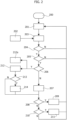
- the frame counter circuit 107 may thus be configured to operate according to the exemplary operation flow illustrated in Figure 2 .
- the frame counter circuit 107 may be reset. Therefore:
- the values of the lower counter threshold FCTL, the upper counter threshold FCTU and the watchdog threshold WDCT may be initialized by reading them from a device memory.
- a device memory may be a writable memory configured to be written as a result of receiving a dedicated frame or message.
- the device D may be waiting for incoming data (e.g., an incoming frame) to be received over the communication bus B. Reception of a frame is exemplified by the data input block 202. Once a frame is received, step 203 may comprise analyzing the received frame. For instance, the received frame may be encoded according to a CAN FD format, and frame analysis performed at step 203 may include check of CRC, bit stuffing, etc.
- the initialization step 201 may be performed before receiving a watchdog trigger (i.e., a toggle event of the watchdog bit), and/or before analyzing a next frame.
- a watchdog trigger i.e., a toggle event of the watchdog bit
- the values of the lower counter threshold FCTL, the upper counter threshold FCTU and the watchdog threshold WDCT may be updated before they are evaluated.
- a step 204 it may be determined, based on the outcome of the analysis step 203, whether the received frame is a valid frame (positive outcome, Y, of block 204) or not (negative outcome, N, of block 204).
- the frame counter circuit 107 may not undertake any action, and operation may continue from step 201, i.e., device D may update the values of the thresholds FCTL, FCTU, WDCT and then continue to wait for frames from the bus B.
- step 205 may comprise determining whether the received frame is addressed to the receiving device D (positive outcome, Y, of block 205) or not (negative outcome, N, of block 205).
- the frame counter circuit 107 may not undertake any action, and operation may continue from step 201, i.e., device D may update the values of the thresholds FCTL, FCTU, WDCT and then continue to wait for frames from the bus B.
- step 205 operation may continue with step 206, where it may be determined whether a watchdog trigger was received at device D (positive outcome, Y, of block 206) or not (negative outcome, N, of block 206).
- step 207 may comprise increasing the value FC of the frame counter (e.g., by one unit).
- step 208 it may be checked whether the current value of the frame counter FC is equal to the lower counter threshold FCTL (positive outcome, Y, of block 208) or not (negative outcome, N, of block 208) .
- the frame counter status output value FCTS may be set (at step 209) to a first value (e.g., 1) indicative of the fact that the number of received frames is within the range of frames expected to be received during the monitoring interval.
- a first value e.g. 1, 1
- operation may continue from step 201.
- step 210 may comprise checking whether the current value of the frame counter FC is equal to the upper counter threshold FCTU (positive outcome, Y, of block 210) or not (negative outcome, N, of block 210).
- the frame counter status output value FCTS may be set (at step 211) to a second value (e.g., 0) indicative of the fact that the number of received frames is not within the range of frames expected to be received during the monitoring interval.
- a second value e.g., 0
- operation may continue from step 201.
- step 210 the frame counter circuit 107 may not undertake any action, and operation may continue from step 201.
- step 212 may comprise increasing the value WDC of the watchdog counter (e.g., by one unit).
- the device D may transmit a frame (e.g., an SPI frame) to communicate the current value of the frame counter status output FCTS, e.g., to a master device coupled to the bus B.
- a frame e.g., an SPI frame
- FCTS frame counter status output
- the device D may transmit such a frame comprising the current value of the frame counter status output FCTS only as a result of the watchdog counter WDC being equal to the watchdog threshold WDCT.
- step 212 operation may continue with a following step 213, which comprises checking whether the current value of the watchdog counter WDC is equal to the watchdog threshold WDCT (positive outcome, Y, of block 213) or not (negative outcome, N, of block 213).
- step 213 operation may continue from step 208.
- step 214 may comprise resetting the value of the frame counter FC and the value of the watchdog counter WDC.
- step 214 may comprise resetting the value of the frame counter status output value FCTS.
- step 214 operation may continue with step 208.
- step 214 operation may continue with step 201.
- steps 204 and 205 (all) valid frames addressed to the device D are counted.
- receiving one of the following frames may result in an increase of the frame counter value FC: unicast frames addressed to the device D, broadcast frames having a chain ID which matches with the chain ID of device D, and are thus addressed to device D, and chain initialization frames.
- receiving one of the following frames may not result in an increase of the frame counter value FC: frames with errors, unicast frames addressed to another device coupled to the bus B (different from device D), broadcast frames having a chain ID which does not match with the chain ID of device D and are thus not addressed to device D, wake-up frames, and synchronization frames.
- the value of the frame counter status output FCTS at the end of a monitoring interval may be used to force the device D to a fail-safe mode. This may be obtained, for instance, in two different ways.
- a master device coupled to the bus B and able to read the value of the frame counter status output FCTS may send a command to force device D into a fail-safe mode.
- the device D may be provided with a watchdog timer, i.e., a timer which is expected to be periodically reset to zero in order to indicate correct operation of the device.
- the device D may be configured to switch to a fail-safe mode as a result of the watchdog timer reaching a certain threshold value. Therefore, one or more embodiments may be configured to prevent resetting the watchdog timer (which in turn would result in the device D switching to the fail-safe mode at expiration of the watchdog timer) as a result of the frame counter status output value FCTS being indicative of a possible communication issue.
- the first option or the second option to force the device D in a fail-safe mode may be selected by means of a configuration bit in a non-volatile memory (NVM) in the device D.
- NVM non-volatile memory
- an electronic device e.g., D
- the electronic device may comprise:
- the controller circuit may be configured to reset said frame counter status bit at the end of said monitoring time interval.
- the frame counter circuit may comprise a modular arithmetic counter circuit (e.g., an up-counter without carry bit) having a certain bit depth, and the frame count value may be constrained to a modulus value of the modular arithmetic counter circuit.
- a modular arithmetic counter circuit e.g., an up-counter without carry bit
- the electronic device may be configured to receive a number j of frames during said monitoring time interval, and the modular arithmetic counter circuit may have a non-zero bit depth equal to or lower than the integer part of log 2 ( j ).
- said comparator circuit may have a bit depth equal to the bit depth of said modular arithmetic counter circuit.
- the modular arithmetic counter circuit may have a non-zero bit depth equal to five or less, preferably a bit depth equal to three, more preferably a bit depth equal to one.
- an electronic device may comprise at least one register configured to store said first frame count threshold value and said second frame count threshold value, the at least one register being accessible via said communication bus in read mode and write mode.
- an electronic device may comprise watchdog sensing circuitry configured to sense watchdog events occurring at certain time intervals and comprising a watchdog event counter circuit configured to provide a watchdog count value of sensed watchdog events.
- the watchdog sensing circuitry may be configured to produce, as a result of a watchdog event being sensed:
- an electronic device may comprise at least one register configured to store said watchdog count threshold value, the at least one register being accessible via said communication bus in read mode and write mode.
- an electronic device may comprise an oscillator circuit (e.g., 106) configured to generate said watchdog events at regular time intervals.
- an oscillator circuit e.g., 106
- sensing watchdog events occurring at certain time intervals may comprise receiving watchdog frames via the communication bus at regular time intervals.
- a controller circuit may be configured to reset said frame count value and optionally said frame counter status bit as a result of receiving a reset command frame via said communication bus.
- a controller circuit may be configured to switch the electronic device to a fail-safe operating mode as a result of the frame counter status bit having said second value indicative of a second (e.g., abnormal) operating status of the electronic device at the end of said monitoring time interval.
- an electronic device may be configured for coupling to a CAN communication bus to receive therefrom digital signals arranged in frames comprising frames encoded according to a CAN FD communication protocol.
- the electronic device may comprise an application-specific integrated circuit configured for controlling communication over the CAN communication bus.
- the application-specific integrated circuit may comprise said check circuit, said frame counter circuit, said comparator circuit and said controller circuit integrated therein.
- a system may comprise a communication bus, at least one electronic device according to one or more embodiments coupled to the communication bus, and a further electronic device coupled to the communication bus and configured to send over the communication bus frames addressed to the at least one electronic device.
- a vehicle e.g., V
- V may comprise a system according to one or more embodiments.
Landscapes
- Engineering & Computer Science (AREA)
- Theoretical Computer Science (AREA)
- Physics & Mathematics (AREA)
- General Engineering & Computer Science (AREA)
- General Physics & Mathematics (AREA)
- Computer Networks & Wireless Communication (AREA)
- Signal Processing (AREA)
- Quality & Reliability (AREA)
- Environmental & Geological Engineering (AREA)
- Computer Hardware Design (AREA)
- Small-Scale Networks (AREA)
- Control Of Vehicle Engines Or Engines For Specific Uses (AREA)
Description
- The invention relates to communication networks involving functional safety features.
- One or more embodiments may find use in automotive networks, e.g., for communication between an electronic control unit (ECU) in a vehicle and one or more corresponding actuator devices and/or sensor devices in the vehicle. Driver circuits for LED lighting modules (e.g., front, rear, interior lights) are exemplary of such devices.
- Data communication in safety-critical systems such as, for instance, certain automotive communication networks may be subject to certain functional safety requirements. For instance, operation of an automotive communication network may involve detecting faults according to the specification described in ISO 26262-6:2018, Appendix D 2.4.
- To this regard, automotive communication networks of known types may implement functional safety features such as cyclic redundancy check (CRC), device addressing and frame counting.
- In particular, frame counting may involve counting the number of frames validly received during a certain time interval at a certain device (e.g., a transceiver) in the communication network, and comparing that number to a number of frames which is expected to be received at that device during that time interval. In other words, a communication network may be designed to detect mismatches between the number of frames sent over the network and the number of frames received over the network in order to detect loss of data and/or insertion of data.
- Communication networks known in the art may implement such a frame counting feature in software, i.e., by means of software code running on a processing unit (e.g., a microcontroller) in an electronic control unit coupled to the network. While such a software implementation may provide a certain degree of flexibility and may allow counting a total number of frames exchanged over the network, it may turn out to be inefficient in connection with some applications, and/or costly.
- In this context, document
US 2018/0007076 A1 discloses a method for detection of attacks on a communication authentication layer of an in-vehicle network. At least one message is received at a node of the in-vehicle network. The received message may include time data and/or location data. Validity of received messages during a first time interval is determined, for instance based on identification, in the received message, of a code from a previously received message. The validity may be determined by a node of in-vehicle network and/or determined by a computing element embedded into in-vehicle network. Once validity of received messages during the first time interval is determined, the number of valid and/or invalid messages is counted for instance by a processor of in-vehicle network. In case that the number of valid messages is less than a first threshold, processor of in-vehicle network checks if the number of invalid messages is greater than a second threshold. In case that the number of invalid messages is greater than a second threshold, an anomaly is determined and the operational mode of the system may be selected. In case that the number of valid messages is not less than a first threshold and/or that the number of invalid messages is not greater than a second threshold, the system returns to determining validity of received messages until the number of valid messages and invalid messages corresponds to the predetermined first and second thresholds respectively. - Document
WO 2019/122589 A1 discloses a communication network to which are connected a master device equipped with a supervision device and multiple slave devices. The communication network is a multiplexed communication network adapted to the transmission of data frames between a master device and at least one slave device in time slots defined in at least one programming table, e.g., LIN or FLEXRAY. The master device and the slave devices transmit frames of data in time slots that are predefined in at least one transverse programming table, known only by the master device. The master device is equipped with a supervision device intended to supervise the operation of each slave device with which the master device must exchange data frames. Each slave device has a parameter p (j) associated with it whenever the latter slave device is declared physically present on the network. A slave device j is declared physically present when the master device transmits (in a write frame) a header requiring a read frame. The analysis means of the supervision device are arranged to increment by one unit a current value of a counter c(j) which is associated with a slave device j whenever the master device does not receive a read frame required from this slave member while the parameter p(j) associated with the slave device is in its first state. Each slave device j has a counter c(j) which is associated with it in addition to its parameter p(j). Finally, the analysis means are arranged so as to consider that there exists a confirmed fault of a slave device j when the counter c(j) associated with the latter reaches a maximum value in a first interval of time predefined. The analysis means can also be arranged to decrement by a unit the current value of the counter c(j) which is associated with a slave device j whenever the master device receives a reading frame of this slave member j while the parameter p(j) associated with the latter is in its first state. In this case, the analysis means consider that a failure of a slave device j is confirmed when the counter c(j) which is associated with the latter reaches the minimum value in a second interval of time predefined. - An object of one or more embodiments is to overcome the above-mentioned drawbacks of the known solutions.
- According to one or more embodiments, such an object can be achieved by means of an electronic device having the features set forth in the claims that follow.
- One or more embodiments relate to a corresponding system.
- One or more embodiments relate to a corresponding vehicle.
- The claims are an integral part of the technical teaching provided herein in respect of the embodiments.
- According to one or more embodiments, an electronic device is provided, the electronic device being configured for coupling to a communication bus to receive therefrom digital signals arranged in frames comprising frames encoded according to a certain communication protocol.
- The electronic device comprises a check circuit sensitive to said digital signals arranged in frames, the check circuit configured to perform a check as to whether a received frame is encoded according to said communication protocol and is addressed to the electronic device.
- The electronic device comprises a frame counter circuit configured to produce a frame count value which is a function of a number of frames received during a monitoring time interval, the frame counter circuit coupled to said check circuit and configured to increase said frame count value as a result of a positive outcome of said check.
- The electronic device comprises a comparator circuit configured to:
- compare said frame count value against a first frame count threshold value and, as a result of said frame count value being equal to said first frame count threshold value, set a frame counter status bit to a first value indicative of a first (i.e. normal) operating status of the electronic device, and
- compare said frame count value against a second frame count threshold value different from said first frame count threshold value and, as a result of said frame count value being equal to said second frame count threshold value, set said frame counter status bit to a second value indicative of a second (i.e. abnormal) operating status of the electronic device.
- The electronic device comprises a controller circuit configured to transmit over the communication bus a frame comprising said frame counter status bit and to reset said frame count value at the end of said monitoring time interval.
- The frame counter circuit comprises a modular arithmetic counter circuit having a certain bit depth, and the frame count value may be constrained to a modulus value of the modular arithmetic counter circuit.
- Therefore, one or more embodiments may provide a frame counter circuit having a low silicon footprint and reduced complexity.
- One or more embodiments will now be described, by way of example only, with reference to the annexed figures, wherein:
-
Figure 1 is a block diagram exemplary of one or more embodiments, and -
Figure 2 is a block diagram exemplary of possible operation of one or more embodiments. - In the ensuing description, one or more specific details are illustrated, aimed at providing an in-depth understanding of examples of embodiments of this description. The embodiments may be obtained without one or more of the specific details, or with other methods, components, materials, etc. In other cases, known structures, materials, or operations are not illustrated or described in detail so that certain aspects of embodiments will not be obscured.
- Reference to "an embodiment" or "one embodiment" in the framework of the present description is intended to indicate that a particular configuration, structure, or characteristic described in relation to the embodiment is comprised in at least one embodiment. Hence, phrases such as "in an embodiment" or "in one embodiment" that may be present in one or more points of the present description do not necessarily refer to one and the same embodiment. Moreover, particular conformations, structures, or characteristics may be combined in any adequate way in one or more embodiments.
- Throughout the figures annexed herein, like parts or elements are indicated with like references/numerals and a corresponding description will not be repeated for brevity.
- The references used herein are provided merely for convenience and hence do not define the extent of protection or the scope of the embodiments.
- By way of introduction to the detailed description of exemplary embodiments, reference may be had to
Figure 1 , which is exemplary of certain components of a device D according to one or more embodiments. - The device D may be configured as a slave or "satellite" device for use in a communication network (e.g., an automotive bus network). For instance, the device D may implement a driver circuit for a LED lighting module in a vehicle. Thus, the device D may receive data frames from a master device (e.g., an ECU in the vehicle, not visible in
Figure 1 ) for controlling operation (e.g., activation and deactivation) of the respective LED lighting module. - The device D may comprise a transceiver circuit TC configured for coupling to a communication bus B to exchange data frames over the bus. The communication bus B may comprise, for instance, a Controller Area Network (CAN) bus.
- The device D may comprise a
controller circuit 10 which manages communication (i.e., frame exchange) over the bus B. Thecontroller circuit 10 may be implemented by means of application-specific hardware (ASIC) to reduce the demand for embedded processors for running software, and may be configured to implement a specific communication protocol. For instance, thecontroller circuit 10 may be configured to exchange, over the bus B, frames encoded according to the format CAN FD, where the bus B operates according to a master-slave architecture. - Therefore, a
controller circuit 10 as exemplified inFigure 1 may comprise: - a
communication controller 100, - a
protocol controller 101, in turn comprising atransmitter circuit 102, a Transmit Error Counter (TEC)circuit 103, areceiver circuit 104 and a Receive Error Counter (REC)circuit 105, and - an
oscillator 106, optionally of a voltage, process and temperature compensated type and/or correspondingly trimmed. - In one or more embodiments, the
transmitter circuit 102 and thereceiver circuit 104 may be configured to cooperate with the transceiver circuit TC (e.g., a CAN FD transceiver circuit) for communicating over the bus B with other devices coupled thereto. For instance, thecommunication controller 100 may send output data TD to theprotocol controller 101, which may process the output data TD to generate a corresponding encoded transmission signal TX which is transmitted over the bus B by the transceiver circuit TC. Similarly, theprotocol controller 101 may receive an encoded reception signal RX from the bus B through the transceiver circuit TC, and may process the encoded reception signal RX to generate corresponding input data RD which are sent to thecommunication controller 100. - In one or more embodiments, the
transmitter circuit 102 may be configured to perform frame preparation (102a), bit stuffing (102b), CRC insertion (102c), frame error check (102d), error counting (102e) and acknowledge (102f). - In one or more embodiments, the
receiver circuit 104 may be configured to perform bit decoding (sampling - 104a), error detection (104b), bit destuffing (104c), CRC verification (104d) and acknowledge generation (104e). - Document
EP 3 547 620 A1 is exemplary of previous activity in this field, which makes it unnecessary providing a more detailed description herein. - It is noted that the occurrence of faults in safety-critical communication systems may result in loss of frames which may lead to safety hazards. For instance, if the communication bus B is used in an automotive lighting system, loss of one or more frames may result in the lights (e.g., the brake lights) failing to properly activate (e.g., turn on) when commanded to do so. According to another example, the communication bus B may be used for collecting data from one or more sensors in the vehicle, so that loss of one or more frames may result in loss of data from the sensors.
- Such loss of frames may be due, for instance, to occasional distortion of communication and/or jitter in frame transmission.
- Therefore, one or more embodiments may aim at detecting mismatches between a number of frames which is expected to be received at a certain device D during a certain monitoring time interval, and a number of frames which is actually received at the device D during that monitoring time interval.
- In particular, since the
communication controller 100 and theprotocol controller 101 may be monolithically integrated into device D (e.g., into the controller circuit 10), a hardware implementation of a frame counter circuit within the device D may be desired. - A first possible solution may involve implementing a so-called "straightforward" counter circuit within the
controller circuit 10. The straightforward counter circuit may be configured to count the total number of frames received at the device D during a monitoring interval and compare it to an expected total number of frames. - The Inventor noted that the number of frames received in a monitoring interval may be fairly high. Purely by way of example, a monitoring interval may last about 10 ms, 50 ms, 100 ms, 150 ms, or other multiples of 10 ms, and the corresponding number of received frames may be approximately equal to 15, 75, 150, 225 (again, these values are provided purely by way of non-limiting examples).
- Therefore, a solution involving a straightforward counter may turn out to be demanding in terms of resources, insofar as a high number of received frames would involve implementation of a large counter in the receiving device.
- Thus, one or more embodiments may aim at detecting a mismatch between the expected number and actual number of frames received at the device D, without the need of keeping track of the total number of frames received during a monitoring interval. As a consequence, the complexity of the frame counter circuit and its occupation of silicon area may be reduced.
- Since a certain number of frames may get corrupted or may be lost (and possibly resent) or may be subject to communication jitter which causes a frame to be received earlier or later than expected, without compromising the safety of the system (i.e., without losing the communication integrity), one or more embodiments may be configured to undertake countermeasures after comparing the number of received frames to one or more threshold values. In other words, a certain tolerance margin may be set, so that the device D may react as a result of the number of received frames being outside of a certain accepted range around the expected number of frames. Optionally, the threshold values may be programmable.
- A device D as exemplified in
Figure 1 , which may comprise acommunication controller 100 and aprotocol controller 101 fully integrated in thecontroller circuit 10, may involve an integrated (i.e., hardware implemented)frame counter circuit 107 configured to: - update a counter value at each valid frame RD received at device D over a certain monitoring interval,
- compare the counter value to one or more reference values (or thresholds),
- detect a frame count mismatch indicative of possible communication failure as a function of said comparison, and
- upon expiration of the monitoring interval, react accordingly to the detection of a communication failure.
- One or more embodiments may advantageously provide a
frame counter circuit 107 having a low hardware complexity, thereby resulting in a cost effective solution. - In one or more embodiments, the
frame counter circuit 107 may be configured to compare the number of received frames to one or more adjustable thresholds, even on a large amount of frames received within a counting period. - In particular, one or more embodiments may rely on the recognition that in real network implementations the difference between received and expected frames may be rather small if compared to the total number of frames exchanged during the monitoring time interval, which makes it unnecessary to count the total (absolute) number of frames received during the monitoring time interval. Instead, modular arithmetic may be resorted to for efficient frame counting.
- For instance, a certain number fE of frames may be expected to be received at the device D during a certain monitoring interval. Based on the functional safety goals of the specific application, the designer of the communication network may thus define the following parameters:


- Purely by way of example, one may consider the following values:


- Still by way of example, by resorting to modulo-16 counting (possibly implemented by means of a simple 4-bit up-counter circuit), the above values may be written as :


- Therefore, one or more embodiments may rely on comparing the number of frames fA (mod i) actually received during a monitoring interval to a lower threshold fL and/or an upper threshold fH in order to determine whether the number of received frames is within an acceptable range or not.
- The Inventor noted that if fE (mod i) is close to zero (e.g., equal to 0 or 1) or close to i (e.g., equal to i-1), then fH (mod i) and tH (mod i) may happen to be lower than fL (mod i) and tL (mod i). Therefore, the designer of the communication network may select the value of i (e.g., by selecting the number of bits of the counter circuit), and/or the duration of the monitoring time interval, so to result in fE (mod i) being sufficiently removed from the extreme values zero and i (e.g., 1 < fE (mod i) < i-1), thereby providing correct operation of the counter circuit under the condition tH (mod i) > tL (mod i) .
- The comparison described above may provide accurate detection of failures as long as the difference between the number of frames actually received fA and the number of expected frames fE is lower than i. In one or more embodiments, such a condition may be assumed to be met, at least insofar as the communication network may comprise additional safety features which are able to detect mismatches between the number of sent and received frames exceeding the value i.
- In one or more embodiments, the duration of the monitoring interval may be determined during a design phase of the device D, depending on the application requirements.
- Alternatively, in one or more embodiments the duration of the monitoring interval may be programmable, possibly on the fly (e.g., the
frame counter circuit 107 may be programmed by means of a dedicated programming frame received over the bus B). - In one or more embodiments, the duration of the monitoring interval may be determined as a function of a watchdog trigger. In particular, a watchdog bit may be stored in a local register within the device D, and the value of the watchdog bit may be toggled at regular time intervals (i.e., periodically). The device D may comprise a watchdog event counter (e.g., a 3-bit counter) which counts the number of toggle events of the watchdog bit. In one or more embodiments, the monitoring interval may terminate as a result of the watchdog event counter reaching a certain threshold value (e.g., five toggle events, three toggle events, or even one toggle event). Thus, the
frame counter circuit 107 may be configured to adopt as monitoring interval the time interval between two consecutive watchdog toggle events, or between every second toggle event, or between every third watchdog toggle event, and so on. - In one or more embodiments, the number of consecutive watchdog toggle events defining a monitoring time interval may be determined during a design phase of the device D, depending on the application requirements.
- Alternatively, in one or more embodiments the number of consecutive watchdog toggle events defining a monitoring time interval may be programmable, possibly on the fly (e.g., the
frame counter circuit 107 may be programmed by means of a dedicated programming frame received over the bus B). Thus, the watchdog event threshold value may be stored in a register which is readable and writable by bus access. Flexible operation of theframe counter circuit 107 may thus be provided, insofar as the number of expected frames between two consecutive watchdog toggle events may not be constant, but may be constant, e.g., between five consecutive watchdog toggle events. - The value of the watchdog bit may be toggled at regular time intervals resorting to various arrangements. For instance, in one or more embodiments the watchdog bit may toggle regularly as driven by the
internal oscillator 106 of thecontroller circuit 10. Additionally or alternatively, the watchdog bit may toggle as a result of a signal received at the device D via the bus B. For instance, the watchdog bit may toggle upon reception of a watchdog frame which is periodically sent over the bus B and received at the device D. - In one or more embodiments, the values of the upper threshold fH and of the lower threshold fL may be determined during a design phase of the device D, depending on the application requirements.
- Alternatively, in one or more embodiments the values of the upper threshold fH and of the lower threshold fL may be programmable, possibly on the fly. Programming the values of the thresholds fH and fL may be useful, for instance, for adapting to different duration of the monitoring time interval, and/or to different applications having different safety requirements. Thus, the upper threshold fH and the lower threshold fL may be stored in registers which are readable and writable by bus access.
- In one or more embodiments, the
frame counter circuit 107 may be reset at the end of each monitoring interval. In some embodiments, reset may be performed (only) at the end of the prescribed monitoring interval, thereby increasing the functional safety at the cost of reduced flexibility of operation. Optionally, arbitrary reset may be performed as a function of a reset signal received at device D from an arbitrary source (e.g., a master device coupled to the bus B). - Therefore, in one or more embodiments the
frame counter circuit 107 may comprise an N-bit up-counter which updates an internal counter value at each valid frame received at the device D. When the N-bit up-counter reaches its maximum value (i.e., 2N-1), it overflows (i.e., it starts counting again from zero) without the need of keeping track of a carry bit. - In general, the N-bit up-counter may have a bit depth lower than the bit depth which would be implemented to count the total number of frames received during a monitoring time interval. For instance, if a number j of frames is expected to be received at the device D over a monitoring time interval, a "straightforward" counter would have a bit depth higher than the integer part of log2(j). The N-bit up-counter according to one or more embodiments may have a bit depth equal to or lower than the integer part of log2(j).
- By way of example, in one or more embodiments the N-bit up-counter may be a 5-bit counter. In another example, the N-bit up-counter may be a 4-bit counter. In another example, the N-bit up-counter may be a 3-bit counter. In another example, the N-bit up-counter may be a 2-bit counter. In certain embodiments, wherein the expected number of faults is low, the N-bit up-counter may be a 1-bit counter.
- The internal counter value may be stored in a register readable by bus access. The register may not be writable by bus access.
- Implementation of the N-bit up-counter with a low number of bits (e.g., any integer lower than or equal to 5) may result in low silicon footprint and reduced complexity of the counter circuit, and/or of the comparator circuit(s).
- As a result of a mismatch between the expected and actual number of received frames being detected, one or more countermeasures may be taken. For instance, a flag signal indicative of a potential problem or failure may be set, and/or the receiving device D may be set (e.g., forced) into a fail-safe mode. Generally, the frame count value may be read via the communication bus B (e.g., by a master device coupled to the bus B).
- In one or more embodiments, the
frame counter circuit 107 may thus be configured to operate according to the exemplary operation flow illustrated inFigure 2 . - At a
reset step 200, theframe counter circuit 107 may be reset. Therefore: - the internal frame counter FC (e.g., a 5-bit value, a 4-bit value, a 3-bit value, a 2-bit value or even a 1-bit value) may be set to zero;
- the frame counter status output value FCTS (e.g., a 1-bit value) indicative of the current status of the
frame counter circuit 107 may be set to zero; - the lower counter threshold FCTL, having the same number of bits of the frame counter FC, may be set to zero;
- the upper counter threshold FCTU, having the same number of bits of the frame counter FC, may be set to zero;
- the watchdog counter WDC (e.g., a 3-bit value) may be set to zero; and
- the watchdog threshold WDCT, having the same number of bits of the watchdog counter WDC, may be set to zero.
- At an
initialization step 201, the values of the lower counter threshold FCTL, the upper counter threshold FCTU and the watchdog threshold WDCT may be initialized by reading them from a device memory. For instance, such a device memory may be a writable memory configured to be written as a result of receiving a dedicated frame or message. - At a
step 203, the device D may be waiting for incoming data (e.g., an incoming frame) to be received over the communication bus B. Reception of a frame is exemplified by thedata input block 202. Once a frame is received,step 203 may comprise analyzing the received frame. For instance, the received frame may be encoded according to a CAN FD format, and frame analysis performed atstep 203 may include check of CRC, bit stuffing, etc. - As exemplified in
Figure 2 , theinitialization step 201 may be performed before receiving a watchdog trigger (i.e., a toggle event of the watchdog bit), and/or before analyzing a next frame. Thus, in one or more embodiments the values of the lower counter threshold FCTL, the upper counter threshold FCTU and the watchdog threshold WDCT may be updated before they are evaluated. - At a
step 204, it may be determined, based on the outcome of theanalysis step 203, whether the received frame is a valid frame (positive outcome, Y, of block 204) or not (negative outcome, N, of block 204). - As a result of a negative outcome of
step 204, theframe counter circuit 107 may not undertake any action, and operation may continue fromstep 201, i.e., device D may update the values of the thresholds FCTL, FCTU, WDCT and then continue to wait for frames from the bus B. - As a result of a positive outcome of
step 204, operation may continue withstep 205, which may comprise determining whether the received frame is addressed to the receiving device D (positive outcome, Y, of block 205) or not (negative outcome, N, of block 205). - As a result of a negative outcome of
step 205, theframe counter circuit 107 may not undertake any action, and operation may continue fromstep 201, i.e., device D may update the values of the thresholds FCTL, FCTU, WDCT and then continue to wait for frames from the bus B. - As a result of a positive outcome of
step 205, operation may continue withstep 206, where it may be determined whether a watchdog trigger was received at device D (positive outcome, Y, of block 206) or not (negative outcome, N, of block 206). - As a result of a negative outcome of
step 206, operation may continue withstep 207, which may comprise increasing the value FC of the frame counter (e.g., by one unit). - At a following
step 208, it may be checked whether the current value of the frame counter FC is equal to the lower counter threshold FCTL (positive outcome, Y, of block 208) or not (negative outcome, N, of block 208) . - As a result of a positive outcome of
step 208, the frame counter status output value FCTS may be set (at step 209) to a first value (e.g., 1) indicative of the fact that the number of received frames is within the range of frames expected to be received during the monitoring interval. After setting the frame counter status output value FCTS to the first value, operation may continue fromstep 201. - As a result of a negative outcome of
step 208, operation may continue withstep 210, which may comprise checking whether the current value of the frame counter FC is equal to the upper counter threshold FCTU (positive outcome, Y, of block 210) or not (negative outcome, N, of block 210). - As a result of a positive outcome of
step 210, the frame counter status output value FCTS may be set (at step 211) to a second value (e.g., 0) indicative of the fact that the number of received frames is not within the range of frames expected to be received during the monitoring interval. After setting the frame counter status output value FCTS to the second value, operation may continue fromstep 201. - As a result of a negative outcome of
step 210, theframe counter circuit 107 may not undertake any action, and operation may continue fromstep 201. - As a result of a positive outcome of
step 206, operation may continue withstep 212, which may comprise increasing the value WDC of the watchdog counter (e.g., by one unit). - Additionally, as a result of a positive outcome of
step 206, the device D may transmit a frame (e.g., an SPI frame) to communicate the current value of the frame counter status output FCTS, e.g., to a master device coupled to the bus B. This operation is schematically exemplified by thedata output block 212a ofFigure 2 . - Alternatively, the device D may transmit such a frame comprising the current value of the frame counter status output FCTS only as a result of the watchdog counter WDC being equal to the watchdog threshold WDCT.
- After
step 212, operation may continue with a followingstep 213, which comprises checking whether the current value of the watchdog counter WDC is equal to the watchdog threshold WDCT (positive outcome, Y, of block 213) or not (negative outcome, N, of block 213). - As a result of a negative outcome of
step 213, operation may continue fromstep 208. - As a result of a positive outcome of
step 213, operation may continue withstep 214, which may comprise resetting the value of the frame counter FC and the value of the watchdog counter WDC. Optionally,step 214 may comprise resetting the value of the frame counter status output value FCTS. - After
step 214, operation may continue withstep 208. Alternatively, afterstep 214 operation may continue withstep 201. - Generally, as a result of
steps - For instance, receiving one of the following frames may result in an increase of the frame counter value FC: unicast frames addressed to the device D, broadcast frames having a chain ID which matches with the chain ID of device D, and are thus addressed to device D, and chain initialization frames.
- On the other hand, as a result of
steps - In one or more embodiments, the value of the frame counter status output FCTS at the end of a monitoring interval (i.e., at the time of a watchdog trigger which causes reset of the frame counter FC and of the watchdog counter WDC) may be used to force the device D to a fail-safe mode. This may be obtained, for instance, in two different ways.
- According to a first option, a master device coupled to the bus B and able to read the value of the frame counter status output FCTS may send a command to force device D into a fail-safe mode.
- According to a second option, the device D may be provided with a watchdog timer, i.e., a timer which is expected to be periodically reset to zero in order to indicate correct operation of the device. In such case, the device D may be configured to switch to a fail-safe mode as a result of the watchdog timer reaching a certain threshold value. Therefore, one or more embodiments may be configured to prevent resetting the watchdog timer (which in turn would result in the device D switching to the fail-safe mode at expiration of the watchdog timer) as a result of the frame counter status output value FCTS being indicative of a possible communication issue.
- In one or more embodiments, the first option or the second option to force the device D in a fail-safe mode may be selected by means of a configuration bit in a non-volatile memory (NVM) in the device D.
- One or more embodiments may thus provide functional safety in a communication network by facilitating detection of:
- repetition of information (insofar as the frame counter circuit counts the received messages including broadcast messages addressed to the device D; in case the number of received messages is higher than the number of expected messages, repetition may be detected);
- loss of information (insofar as the frame counter circuit counts the received messages including broadcast messages addressed to the device D; in case the number of received messages is lower than the number of expected messages, loss of information may be detected);
- delay of information (e.g., in case the number of counted messages at a certain frame counter reset instant is lower than expected and at a subsequent frame counter reset instant it is higher than expected; this condition may be indicative of the fact that either information is lost in a first monitoring interval and repeated in a subsequent second monitoring interval, or that information is delayed from one monitoring interval to the next one);
- insertion of information (which may be detected in the same way as repetition of information);
- masquerade or incorrect addressing of information (insofar as incorrectly addressed frames may cause one device in the network to receive more frames than expected and another device in the network to receive less frames than expected);
- incorrect sequence of information (e.g., by reading back the frame counter content immediately after the frame has been sent; the expected frame counter content is compared to the real frame counter content belonging to this message, and an incorrect sequence may be detected in case the message counter content does not match with the expected value);
- corruption of information (insofar as corruption of information is detected by a non-matching CRC value, which causes the incoming frame being dropped and not counted since it is classified as invalid; as a result, the frame counter value may be lower than expected and a corrupted frame may be detected);
- asymmetric information sent from a sender to multiple receivers (e.g., insofar as in CAN FD Light networks every message may be addressed to a dedicated receiver; addressing to multiple receivers may be caused either by a corrupted frame or by an incorrectly operating receiver device which takes messages not addressed to it; in the former case, a corrupted frame may be detected by a CRC mismatch, while in the latter case, incorrect operation of the receiver device may be detected since the corresponding frame counter has a value higher than expected);
- information from a sender received by only a subset of the intended receivers (insofar as the devices which did not receive a message intended for them may have a frame counter value which is lower than expected; therefore, a similar detection as for the "loss of information" case may take place);
- blocking access to a communication channel (frames that are not received by the receivers are not counter and the corresponding frame counter value does not match the expected value; if the master sends a unicast message and it does not receive an answer, the block of the communication channel may be also detected; if the unicast frame toggling the watchdog is blocked, the watchdog is not operated and the device may eventually enter a fail-safe state).
- As exemplified herein, an electronic device (e.g., D) may be configured for coupling (e.g., TC) to a communication bus (e.g., B) to receive therefrom digital signals arranged in frames comprising frames encoded according to a certain communication protocol. The electronic device may comprise:
- a check circuit sensitive to said digital signals arranged in frames, the check circuit configured to perform a check (e.g., 203, 204, 205) as to whether a received frame is encoded according to said communication protocol and is addressed to the electronic device,
- a frame counter circuit configured to produce a frame count value which is a function of a number of frames received during a monitoring time interval, the frame counter circuit coupled to said check circuit and configured to increase said frame count value as a result of a positive outcome of said check,
- a comparator circuit configured to:
- compare (e.g., 208) said frame count value against a first frame count threshold value and, as a result of said frame count value being equal to said first frame count threshold value, set a frame counter status bit to a first value indicative of a first (i.e. normal) operating status of the electronic device,
- compare (e.g., 210) said frame count value against a second frame count threshold value different from said first frame count threshold value and, as a result of said frame count value being equal to said second frame count threshold value, set said frame counter status bit to a second value indicative of a second (i.e. abnormal) operating status of the electronic device,
- a controller circuit (e.g., 10) configured to transmit (e.g., 212a) over the communication bus a frame comprising said frame counter status bit and to reset (e.g., 214) said frame count value at the end of said monitoring time interval.
- As exemplified herein, the controller circuit may be configured to reset said frame counter status bit at the end of said monitoring time interval.
- As exemplified herein, the frame counter circuit may comprise a modular arithmetic counter circuit (e.g., an up-counter without carry bit) having a certain bit depth, and the frame count value may be constrained to a modulus value of the modular arithmetic counter circuit.
- As exemplified herein, the electronic device may be configured to receive a number j of frames during said monitoring time interval, and the modular arithmetic counter circuit may have a non-zero bit depth equal to or lower than the integer part of log2(j).
- As exemplified herein, said comparator circuit may have a bit depth equal to the bit depth of said modular arithmetic counter circuit.
- As exemplified herein, the modular arithmetic counter circuit may have a non-zero bit depth equal to five or less, preferably a bit depth equal to three, more preferably a bit depth equal to one.
- As exemplified herein, an electronic device may comprise at least one register configured to store said first frame count threshold value and said second frame count threshold value, the at least one register being accessible via said communication bus in read mode and write mode.
- As exemplified herein, an electronic device may comprise watchdog sensing circuitry configured to sense watchdog events occurring at certain time intervals and comprising a watchdog event counter circuit configured to provide a watchdog count value of sensed watchdog events. The watchdog sensing circuitry may be configured to produce, as a result of a watchdog event being sensed:
- transmission over the communication bus of a frame comprising said frame counter status bit,
- an increase in said watchdog count value,
- comparison (e.g., 213) of said watchdog count value to a watchdog count threshold value and, as a result of said watchdog count value being equal to said watchdog count threshold value, a reset of said frame count value and of said watchdog count value, and optionally a reset of said frame counter status bit.
- As exemplified herein, an electronic device may comprise at least one register configured to store said watchdog count threshold value, the at least one register being accessible via said communication bus in read mode and write mode.
- As exemplified herein, an electronic device may comprise an oscillator circuit (e.g., 106) configured to generate said watchdog events at regular time intervals.
- As exemplified herein, sensing watchdog events occurring at certain time intervals may comprise receiving watchdog frames via the communication bus at regular time intervals.
- As exemplified herein, a controller circuit may be configured to reset said frame count value and optionally said frame counter status bit as a result of receiving a reset command frame via said communication bus.
- As exemplified herein, a controller circuit may be configured to switch the electronic device to a fail-safe operating mode as a result of the frame counter status bit having said second value indicative of a second (e.g., abnormal) operating status of the electronic device at the end of said monitoring time interval.
- As exemplified herein, an electronic device may be configured for coupling to a CAN communication bus to receive therefrom digital signals arranged in frames comprising frames encoded according to a CAN FD communication protocol. The electronic device may comprise an application-specific integrated circuit configured for controlling communication over the CAN communication bus. The application-specific integrated circuit may comprise said check circuit, said frame counter circuit, said comparator circuit and said controller circuit integrated therein.
- As exemplified herein, a system may comprise a communication bus, at least one electronic device according to one or more embodiments coupled to the communication bus, and a further electronic device coupled to the communication bus and configured to send over the communication bus frames addressed to the at least one electronic device.
- As exemplified herein, a vehicle (e.g., V) may comprise a system according to one or more embodiments.
- Without prejudice to the underlying principles, the details and embodiments may vary, even significantly, with respect to what has been described by way of example only, without departing from the extent of protection.
- The extent of protection is defined by the annexed claims.
Claims (13)
- An electronic device (D) configured for coupling (TC) to a communication bus (B) to receive therefrom digital signals arranged in frames comprising frames encoded according to a certain communication protocol, the electronic device (D) being configured to receive a number j of frames during a monitoring time interval, the electronic device (D) comprising:a check circuit sensitive to said digital signals arranged in frames, the check circuit configured to perform a check (203, 204, 205) as to whether a received frame is encoded according to said communication protocol and is addressed to the electronic device (D),a frame counter circuit configured to produce a frame count value which is a function of a number of frames received during said monitoring time interval, the frame counter circuit coupled to said check circuit and configured to increase said frame count value as a result of a positive outcome of said check (203, 204, 205),a comparator circuit configured to:compare (208) said frame count value against a first frame count threshold value and, as a result of said frame count value being equal to said first frame count threshold value, set a frame counter status bit to a first value indicative of a normal operating status of the electronic device (D), andcompare (210) said frame count value against a second frame count threshold value different from said first frame count threshold value and, as a result of said frame count value being equal to said second frame count threshold value, set said frame counter status bit to a second value indicative of an abnormal operating status of the electronic device (D),a controller circuit (10) configured to transmit (212a) over the communication bus (B) a frame comprising said frame counter status bit and to reset (214) said frame count value at the end of said monitoring time interval,wherein the frame counter circuit comprises a modular arithmetic counter circuit having a non-zero bit depth equal to or lower than the integer part of log2(j), and wherein said frame count value is constrained to a modulus value of said modular arithmetic counter circuit.
- The electronic device (D) of claim 1, wherein said comparator circuit has a bit depth equal to said bit depth of said modular arithmetic counter circuit.
- The electronic device (D) of any of the previous claims, wherein the modular arithmetic counter circuit has a non-zero bit depth equal to five or less, preferably a bit depth equal to three, more preferably a bit depth equal to one.
- The electronic device (D) of any of the previous claims, comprising at least one register configured to store said first frame count threshold value and said second frame count threshold value, wherein said at least one register is accessible via said communication bus (B) in read mode and write mode.
- The electronic device (D) of any of the previous claims, comprising watchdog sensing circuitry configured to sense watchdog events occurring at certain time intervals and comprising a watchdog event counter circuit configured to provide a watchdog count value of sensed watchdog events, wherein said watchdog sensing circuitry is configured to produce, as a result of a watchdog event being sensed:transmission over the communication bus (B) of a frame comprising said frame counter status bit,an increase in said watchdog count value,comparison (213) of said watchdog count value to a watchdog count threshold value and, as a result of said watchdog count value being equal to said watchdog count threshold value, a reset (214) of said frame count value and of said watchdog count value.
- The electronic device (D) of claim 5, comprising at least one register configured to store said watchdog count threshold value, wherein said at least one register is accessible via said communication bus (B) in read mode and write mode.
- The electronic device (D) of claim 5 or claim 6, comprising an oscillator circuit (106) configured to generate said watchdog events at regular time intervals.
- The electronic device (D) of any of claims 5 to 7, wherein sensing watchdog events occurring at certain time intervals comprises receiving watchdog frames via the communication bus (B) at regular time intervals.
- The electronic device (D) of any of the previous claims, wherein the controller circuit (10) is configured to reset (214) said frame count value as a result of receiving a reset command frame via said communication bus (B).
- The electronic device (D) of any of the previous claims, wherein the controller circuit (10) is configured to switch the electronic device (D) to a fail-safe operating mode as a result of the frame counter status bit having said second value indicative of a second operating status of the electronic device (D) at the end of said monitoring time interval.
- The electronic device (D) of any of the previous claims, configured for coupling (TC) to a CAN communication bus (B) to receive therefrom digital signals arranged in frames comprising frames encoded according to a CAN FD communication protocol, wherein the electronic device (D) comprises an application-specific integrated circuit configured for controlling communication over the CAN communication bus (B), the application-specific integrated circuit comprising said check circuit, said frame counter circuit, said comparator circuit and said controller circuit integrated therein.
- A system comprising a communication bus (B), at least one electronic device (D) according to any of the previous claims, the at least one electronic device (D) coupled to the communication bus (B), and a further electronic device coupled to the communication bus (B) and configured to send over the communication bus (B) frames addressed to the at least one electronic device (D) .
- A vehicle (V) comprising a system according to claim 12.
Applications Claiming Priority (1)
| Application Number | Priority Date | Filing Date | Title |
|---|---|---|---|
| IT102020000004978A IT202000004978A1 (en) | 2020-03-09 | 2020-03-09 | CORRESPONDING ELECTRONIC DEVICE, SYSTEM AND VEHICLE |
Publications (3)
| Publication Number | Publication Date |
|---|---|
| EP3879730A1 EP3879730A1 (en) | 2021-09-15 |
| EP3879730B1 true EP3879730B1 (en) | 2023-07-19 |
| EP3879730C0 EP3879730C0 (en) | 2023-07-19 |
Family
ID=70480800
Family Applications (1)
| Application Number | Title | Priority Date | Filing Date |
|---|---|---|---|
| EP21158711.8A Active EP3879730B1 (en) | 2020-03-09 | 2021-02-23 | An electronic device, a corresponding communication system and a vehicle comprising the system |
Country Status (4)
| Country | Link |
|---|---|
| US (2) | US11677648B2 (en) |
| EP (1) | EP3879730B1 (en) |
| CN (1) | CN113438139B (en) |
| IT (1) | IT202000004978A1 (en) |
Families Citing this family (10)
| Publication number | Priority date | Publication date | Assignee | Title |
|---|---|---|---|---|
| DE102019207174A1 (en) * | 2019-05-16 | 2020-11-19 | Robert Bosch Gmbh | Transmitting / receiving device and communication control device for a subscriber station of a serial bus system and method for communication in a serial bus system |
| IT202000004978A1 (en) * | 2020-03-09 | 2021-09-09 | Stmicroelectronics Application Gmbh | CORRESPONDING ELECTRONIC DEVICE, SYSTEM AND VEHICLE |
| CN114090308B (en) * | 2021-10-14 | 2025-09-26 | 武汉光庭信息技术股份有限公司 | A method and system for evaluating the effectiveness of important display functions of a display device |
| CN114089157B (en) * | 2021-11-02 | 2024-04-12 | 广州昂宝电子有限公司 | Chip testing method and system |
| US11631376B1 (en) * | 2022-01-13 | 2023-04-18 | Stmicroelectronics S.R.L. | System architecture for high density mini/micro LED backlight application |
| US12362963B2 (en) | 2022-08-02 | 2025-07-15 | Stmicroelectronics Application Gmbh | Electronic device, corresponding bus communication system and method of configuring a bus communication system |
| IT202200020490A1 (en) | 2022-08-02 | 2024-04-05 | Stmicroelectronics Application Gmbh | Electronic device, corresponding bus communication system and procedure for configuring a bus communication system |
| FR3167505A1 (en) * | 2024-10-15 | 2026-04-17 | Stellantis Auto Sas | Method for supervising a computer network of a motor vehicle |
| CN119728614B (en) * | 2024-12-16 | 2025-10-28 | 北京中科泰佳电子科技有限公司 | Periodic message sending method and device for 429 bus |
| KR102996322B1 (en) | 2026-05-18 | 2026-07-24 | 국방과학연구소 | High-speed CAN communication message processing device and method |
Family Cites Families (21)
| Publication number | Priority date | Publication date | Assignee | Title |
|---|---|---|---|---|
| JPH10107805A (en) * | 1996-09-30 | 1998-04-24 | Mazda Motor Corp | Multiplex transmission equipment |
| US7346819B2 (en) * | 2004-10-29 | 2008-03-18 | Rambus Inc. | Through-core self-test with multiple loopbacks |
| KR100901124B1 (en) | 2007-02-27 | 2009-06-08 | 삼성전자주식회사 | Electric field determination method of digital multimedia broadcasting and portable terminal using same |
| JP5904050B2 (en) * | 2012-08-03 | 2016-04-13 | ソニー株式会社 | Power storage device |
| US9389949B1 (en) | 2013-12-06 | 2016-07-12 | Rockwell Collins, Inc. | Optical fiber signal quality measuring and reporting in aviation systems and related method |
| KR101638613B1 (en) * | 2015-04-17 | 2016-07-11 | 현대자동차주식회사 | In-vehicle network intrusion detection system and method for controlling the same |
| US9989575B2 (en) | 2015-04-30 | 2018-06-05 | GM Global Technology Operations LLC | Detection of ECU ground fault with can bus voltage measurements |
| US9904587B1 (en) * | 2015-12-18 | 2018-02-27 | Amazon Technologies, Inc. | Detecting anomalous behavior in an electronic environment using hardware-based information |
| WO2017119246A1 (en) * | 2016-01-08 | 2017-07-13 | パナソニック インテレクチュアル プロパティ コーポレーション オブ アメリカ | Abnormality detection method, abnormality detection device, and abnormality detection system |
| CN106123476B (en) * | 2016-06-27 | 2018-11-16 | 青岛海尔股份有限公司 | Intelligent detecting method for refrigerator |
| EP3264718B1 (en) * | 2016-06-29 | 2021-03-03 | Argus Cyber Security Ltd | System and method for detection and prevention of attacks on in-vehicle networks |
| CN106790053B (en) | 2016-12-20 | 2019-08-27 | 江苏大学 | A method for ECU safe communication in CAN bus |
| JP2018133744A (en) | 2017-02-16 | 2018-08-23 | パナソニックIpマネジメント株式会社 | Communication system, vehicle, and monitoring method |
| EP3404873B1 (en) | 2017-05-18 | 2019-10-02 | Melexis Technologies NV | Low-power data bus receiver |
| FR3076161B1 (en) * | 2017-12-21 | 2019-11-15 | Psa Automobiles Sa | (EN) SLAVE ORGAN FAULT SUPERVISION DEVICE (S) FOR A MASTER ORGAN OF A MULTIPLEX NETWORK. |
| JP6984512B2 (en) * | 2018-03-22 | 2021-12-22 | 株式会社デンソー | Electronic control device |
| IT201800003980A1 (en) | 2018-03-26 | 2019-09-26 | Stmicroelectronics Application Gmbh | COMMUNICATION PROCESS, SYSTEM, DEVICES, SIGNAL AND CORRESPONDING VEHICLE |
| US10632315B2 (en) * | 2018-05-10 | 2020-04-28 | Pacesetter, Inc. | Managing communication interference in leadless dual chamber pacing systems and other IMD systems |
| CN109309598B (en) | 2018-08-01 | 2021-03-23 | 惠州市德赛西威汽车电子股份有限公司 | Sampling point automatic test system and method for tested vehicle-mounted module with CAN function |
| US10838794B2 (en) * | 2018-08-21 | 2020-11-17 | Hamilton Sunstrand Corporation | Rate based fault restart scheme |
| IT202000004978A1 (en) * | 2020-03-09 | 2021-09-09 | Stmicroelectronics Application Gmbh | CORRESPONDING ELECTRONIC DEVICE, SYSTEM AND VEHICLE |
-
2020
- 2020-03-09 IT IT102020000004978A patent/IT202000004978A1/en unknown
-
2021
- 2021-02-23 US US17/182,914 patent/US11677648B2/en active Active
- 2021-02-23 EP EP21158711.8A patent/EP3879730B1/en active Active
- 2021-03-04 CN CN202110241466.0A patent/CN113438139B/en active Active
-
2023
- 2023-04-28 US US18/309,397 patent/US12332727B2/en active Active
Also Published As
| Publication number | Publication date |
|---|---|
| CN113438139B (en) | 2022-12-16 |
| US20230269150A1 (en) | 2023-08-24 |
| US11677648B2 (en) | 2023-06-13 |
| US20210281497A1 (en) | 2021-09-09 |
| US12332727B2 (en) | 2025-06-17 |
| CN113438139A (en) | 2021-09-24 |
| EP3879730C0 (en) | 2023-07-19 |
| IT202000004978A1 (en) | 2021-09-09 |
| EP3879730A1 (en) | 2021-09-15 |
Similar Documents
| Publication | Publication Date | Title |
|---|---|---|
| US12332727B2 (en) | Device and method for checking frames from a communication bus | |
| CN113691430B (en) | Method for operating a communication bus, corresponding system, device and vehicle | |
| KR102943009B1 (en) | Error detection test device for subscriber stations of serial bus systems and test method for error detection mechanism during communication in serial bus systems | |
| CN107078931B (en) | Method for serial transmission of frames from sender to receiver and bus system | |
| US7047475B2 (en) | CRC encoding scheme for conveying status information | |
| US7890229B2 (en) | Method and device for waking users of a bus system, and corresponding users | |
| US7327735B2 (en) | System and method for detecting lost messages transmitted between modules in a communication device | |
| US20100014439A1 (en) | Node of a distributed communication system, node and monitoring device coupled to such communication system | |
| EP2712123A1 (en) | Standard CAN implementation tolerating CAN FD frames | |
| CN110365564A (en) | Communication method and corresponding system and device | |
| CN101647234B (en) | The method and system of the cyclical transmission process waiting for transmission data for safety | |
| KR20150004833A (en) | Subscriber station for a bus system and method for transmitting messages between subscriber stations of a bus system | |
| EP1879331B1 (en) | Communication network system and error verification method | |
| Specification | Bosch | |
| CN102884744B (en) | For protecting up for the method and apparatus of the packet transmitted by interface | |
| US20050268166A1 (en) | Circuit for detecting ground offset of parts of a network | |
| US7808917B2 (en) | Method and system for transmitting telegrams | |
| JP4570753B2 (en) | Error code sending apparatus and method | |
| US20250258792A1 (en) | Subscriber station for a serial bus system, and method for communication in a serial bus system | |
| Dais et al. | Impact of Bit Representation on Transport Capacity and Clock Accuracy in Serial Data Streams | |
| GB2607254A (en) | Transmitting/receiving device for a subscriber station of a serial bus system, and method for communication in a serial bus system | |
| JPH04142132A (en) | Local network controller |
Legal Events
| Date | Code | Title | Description |
|---|---|---|---|
| PUAI | Public reference made under article 153(3) epc to a published international application that has entered the european phase |
Free format text: ORIGINAL CODE: 0009012 |
|
| STAA | Information on the status of an ep patent application or granted ep patent |
Free format text: STATUS: THE APPLICATION HAS BEEN PUBLISHED |
|
| AK | Designated contracting states |
Kind code of ref document: A1 Designated state(s): AL AT BE BG CH CY CZ DE DK EE ES FI FR GB GR HR HU IE IS IT LI LT LU LV MC MK MT NL NO PL PT RO RS SE SI SK SM TR |
|
| STAA | Information on the status of an ep patent application or granted ep patent |
Free format text: STATUS: REQUEST FOR EXAMINATION WAS MADE |
|
| 17P | Request for examination filed |
Effective date: 20220308 |
|
| RBV | Designated contracting states (corrected) |
Designated state(s): AL AT BE BG CH CY CZ DE DK EE ES FI FR GB GR HR HU IE IS IT LI LT LU LV MC MK MT NL NO PL PT RO RS SE SI SK SM TR |
|
| GRAP | Despatch of communication of intention to grant a patent |
Free format text: ORIGINAL CODE: EPIDOSNIGR1 |
|
| STAA | Information on the status of an ep patent application or granted ep patent |
Free format text: STATUS: GRANT OF PATENT IS INTENDED |
|
| RIC1 | Information provided on ipc code assigned before grant |
Ipc: B60R 16/023 20060101ALN20230302BHEP Ipc: G06F 11/07 20060101ALI20230302BHEP Ipc: H04L 12/403 20060101ALI20230302BHEP Ipc: H04L 12/40 20060101ALI20230302BHEP Ipc: H04L 1/00 20060101AFI20230302BHEP |
|
| INTG | Intention to grant announced |
Effective date: 20230316 |
|
| RIN1 | Information on inventor provided before grant (corrected) |
Inventor name: RENNIG, FRED |
|
| GRAS | Grant fee paid |
Free format text: ORIGINAL CODE: EPIDOSNIGR3 |
|
| GRAA | (expected) grant |
Free format text: ORIGINAL CODE: 0009210 |
|
| STAA | Information on the status of an ep patent application or granted ep patent |
Free format text: STATUS: THE PATENT HAS BEEN GRANTED |
|
| AK | Designated contracting states |
Kind code of ref document: B1 Designated state(s): AL AT BE BG CH CY CZ DE DK EE ES FI FR GB GR HR HU IE IS IT LI LT LU LV MC MK MT NL NO PL PT RO RS SE SI SK SM TR |
|
| REG | Reference to a national code |
Ref country code: GB Ref legal event code: FG4D |
|
| REG | Reference to a national code |
Ref country code: CH Ref legal event code: EP |
|
| REG | Reference to a national code |
Ref country code: DE Ref legal event code: R096 Ref document number: 602021003515 Country of ref document: DE |
|
| REG | Reference to a national code |
Ref country code: IE Ref legal event code: FG4D |
|
| U01 | Request for unitary effect filed |
Effective date: 20230726 |
|
| U07 | Unitary effect registered |
Designated state(s): AT BE BG DE DK EE FI FR IT LT LU LV MT NL PT SE SI Effective date: 20230801 |
|
| REG | Reference to a national code |
Ref country code: LT Ref legal event code: MG9D |
|
| PG25 | Lapsed in a contracting state [announced via postgrant information from national office to epo] |
Ref country code: GR Free format text: LAPSE BECAUSE OF FAILURE TO SUBMIT A TRANSLATION OF THE DESCRIPTION OR TO PAY THE FEE WITHIN THE PRESCRIBED TIME-LIMIT Effective date: 20231020 |
|
| PG25 | Lapsed in a contracting state [announced via postgrant information from national office to epo] |
Ref country code: IS Free format text: LAPSE BECAUSE OF FAILURE TO SUBMIT A TRANSLATION OF THE DESCRIPTION OR TO PAY THE FEE WITHIN THE PRESCRIBED TIME-LIMIT Effective date: 20231119 |
|
| PG25 | Lapsed in a contracting state [announced via postgrant information from national office to epo] |
Ref country code: RS Free format text: LAPSE BECAUSE OF FAILURE TO SUBMIT A TRANSLATION OF THE DESCRIPTION OR TO PAY THE FEE WITHIN THE PRESCRIBED TIME-LIMIT Effective date: 20230719 Ref country code: NO Free format text: LAPSE BECAUSE OF FAILURE TO SUBMIT A TRANSLATION OF THE DESCRIPTION OR TO PAY THE FEE WITHIN THE PRESCRIBED TIME-LIMIT Effective date: 20231019 Ref country code: IS Free format text: LAPSE BECAUSE OF FAILURE TO SUBMIT A TRANSLATION OF THE DESCRIPTION OR TO PAY THE FEE WITHIN THE PRESCRIBED TIME-LIMIT Effective date: 20231119 Ref country code: HR Free format text: LAPSE BECAUSE OF FAILURE TO SUBMIT A TRANSLATION OF THE DESCRIPTION OR TO PAY THE FEE WITHIN THE PRESCRIBED TIME-LIMIT Effective date: 20230719 Ref country code: GR Free format text: LAPSE BECAUSE OF FAILURE TO SUBMIT A TRANSLATION OF THE DESCRIPTION OR TO PAY THE FEE WITHIN THE PRESCRIBED TIME-LIMIT Effective date: 20231020 |
|
| U20 | Renewal fee for the european patent with unitary effect paid |
Year of fee payment: 4 Effective date: 20240123 |
|
| PG25 | Lapsed in a contracting state [announced via postgrant information from national office to epo] |
Ref country code: PL Free format text: LAPSE BECAUSE OF FAILURE TO SUBMIT A TRANSLATION OF THE DESCRIPTION OR TO PAY THE FEE WITHIN THE PRESCRIBED TIME-LIMIT Effective date: 20230719 |
|
| REG | Reference to a national code |
Ref country code: DE Ref legal event code: R097 Ref document number: 602021003515 Country of ref document: DE |
|
| PG25 | Lapsed in a contracting state [announced via postgrant information from national office to epo] |
Ref country code: ES Free format text: LAPSE BECAUSE OF FAILURE TO SUBMIT A TRANSLATION OF THE DESCRIPTION OR TO PAY THE FEE WITHIN THE PRESCRIBED TIME-LIMIT Effective date: 20230719 |
|
| PG25 | Lapsed in a contracting state [announced via postgrant information from national office to epo] |
Ref country code: SM Free format text: LAPSE BECAUSE OF FAILURE TO SUBMIT A TRANSLATION OF THE DESCRIPTION OR TO PAY THE FEE WITHIN THE PRESCRIBED TIME-LIMIT Effective date: 20230719 Ref country code: RO Free format text: LAPSE BECAUSE OF FAILURE TO SUBMIT A TRANSLATION OF THE DESCRIPTION OR TO PAY THE FEE WITHIN THE PRESCRIBED TIME-LIMIT Effective date: 20230719 Ref country code: ES Free format text: LAPSE BECAUSE OF FAILURE TO SUBMIT A TRANSLATION OF THE DESCRIPTION OR TO PAY THE FEE WITHIN THE PRESCRIBED TIME-LIMIT Effective date: 20230719 Ref country code: CZ Free format text: LAPSE BECAUSE OF FAILURE TO SUBMIT A TRANSLATION OF THE DESCRIPTION OR TO PAY THE FEE WITHIN THE PRESCRIBED TIME-LIMIT Effective date: 20230719 Ref country code: SK Free format text: LAPSE BECAUSE OF FAILURE TO SUBMIT A TRANSLATION OF THE DESCRIPTION OR TO PAY THE FEE WITHIN THE PRESCRIBED TIME-LIMIT Effective date: 20230719 |
|
| PLBE | No opposition filed within time limit |
Free format text: ORIGINAL CODE: 0009261 |
|
| STAA | Information on the status of an ep patent application or granted ep patent |
Free format text: STATUS: NO OPPOSITION FILED WITHIN TIME LIMIT |
|
| 26N | No opposition filed |
Effective date: 20240422 |
|
| U1N | Appointed representative for the unitary patent procedure changed after the registration of the unitary effect |
Representative=s name: BUZZI, NOTARO & ANTONIELLI D'OULX S.P.A.; IT |
|
| PG25 | Lapsed in a contracting state [announced via postgrant information from national office to epo] |
Ref country code: MC Free format text: LAPSE BECAUSE OF FAILURE TO SUBMIT A TRANSLATION OF THE DESCRIPTION OR TO PAY THE FEE WITHIN THE PRESCRIBED TIME-LIMIT Effective date: 20230719 |
|
| REG | Reference to a national code |
Ref country code: CH Ref legal event code: PL |
|
| PG25 | Lapsed in a contracting state [announced via postgrant information from national office to epo] |
Ref country code: CH Free format text: LAPSE BECAUSE OF NON-PAYMENT OF DUE FEES Effective date: 20240229 |
|
| PG25 | Lapsed in a contracting state [announced via postgrant information from national office to epo] |
Ref country code: CH Free format text: LAPSE BECAUSE OF NON-PAYMENT OF DUE FEES Effective date: 20240229 |
|
| PG25 | Lapsed in a contracting state [announced via postgrant information from national office to epo] |
Ref country code: IE Free format text: LAPSE BECAUSE OF NON-PAYMENT OF DUE FEES Effective date: 20240223 |
|
| PG25 | Lapsed in a contracting state [announced via postgrant information from national office to epo] |
Ref country code: IE Free format text: LAPSE BECAUSE OF NON-PAYMENT OF DUE FEES Effective date: 20240223 |
|
| U20 | Renewal fee for the european patent with unitary effect paid |
Year of fee payment: 5 Effective date: 20250121 |
|
| PG25 | Lapsed in a contracting state [announced via postgrant information from national office to epo] |
Ref country code: CY Free format text: LAPSE BECAUSE OF FAILURE TO SUBMIT A TRANSLATION OF THE DESCRIPTION OR TO PAY THE FEE WITHIN THE PRESCRIBED TIME-LIMIT; INVALID AB INITIO Effective date: 20210223 |
|
| PG25 | Lapsed in a contracting state [announced via postgrant information from national office to epo] |
Ref country code: HU Free format text: LAPSE BECAUSE OF FAILURE TO SUBMIT A TRANSLATION OF THE DESCRIPTION OR TO PAY THE FEE WITHIN THE PRESCRIBED TIME-LIMIT; INVALID AB INITIO Effective date: 20210223 |
|
| GBPC | Gb: european patent ceased through non-payment of renewal fee |
Effective date: 20250223 |
|
| PG25 | Lapsed in a contracting state [announced via postgrant information from national office to epo] |
Ref country code: TR Free format text: LAPSE BECAUSE OF FAILURE TO SUBMIT A TRANSLATION OF THE DESCRIPTION OR TO PAY THE FEE WITHIN THE PRESCRIBED TIME-LIMIT Effective date: 20230719 |
|
| PG25 | Lapsed in a contracting state [announced via postgrant information from national office to epo] |
Ref country code: GB Free format text: LAPSE BECAUSE OF NON-PAYMENT OF DUE FEES Effective date: 20250223 |
|
| U20 | Renewal fee for the european patent with unitary effect paid |
Year of fee payment: 6 Effective date: 20260121 |