EP3879586A1 - Light-emitting element - Google Patents
Light-emitting element Download PDFInfo
- Publication number
- EP3879586A1 EP3879586A1 EP19881942.7A EP19881942A EP3879586A1 EP 3879586 A1 EP3879586 A1 EP 3879586A1 EP 19881942 A EP19881942 A EP 19881942A EP 3879586 A1 EP3879586 A1 EP 3879586A1
- Authority
- EP
- European Patent Office
- Prior art keywords
- light emitting
- light
- shielding layer
- emitting part
- substrate
- Prior art date
- Legal status (The legal status is an assumption and is not a legal conclusion. Google has not performed a legal analysis and makes no representation as to the accuracy of the status listed.)
- Pending
Links
- 239000000758 substrate Substances 0.000 claims abstract description 54
- 238000000605 extraction Methods 0.000 claims description 18
- 239000004065 semiconductor Substances 0.000 description 53
- 238000000034 method Methods 0.000 description 18
- 238000005530 etching Methods 0.000 description 7
- 229910002601 GaN Inorganic materials 0.000 description 5
- JMASRVWKEDWRBT-UHFFFAOYSA-N Gallium nitride Chemical compound [Ga]#N JMASRVWKEDWRBT-UHFFFAOYSA-N 0.000 description 5
- 238000005229 chemical vapour deposition Methods 0.000 description 5
- VYPSYNLAJGMNEJ-UHFFFAOYSA-N Silicium dioxide Chemical compound O=[Si]=O VYPSYNLAJGMNEJ-UHFFFAOYSA-N 0.000 description 4
- GWEVSGVZZGPLCZ-UHFFFAOYSA-N Titan oxide Chemical compound O=[Ti]=O GWEVSGVZZGPLCZ-UHFFFAOYSA-N 0.000 description 4
- 238000002248 hydride vapour-phase epitaxy Methods 0.000 description 4
- 238000004519 manufacturing process Methods 0.000 description 4
- 238000001451 molecular beam epitaxy Methods 0.000 description 4
- 238000002161 passivation Methods 0.000 description 4
- 238000005240 physical vapour deposition Methods 0.000 description 4
- 239000003086 colorant Substances 0.000 description 3
- 230000007423 decrease Effects 0.000 description 3
- 239000000463 material Substances 0.000 description 3
- WHEATZOONURNGF-UHFFFAOYSA-N benzocyclobutadiene Chemical compound C1=CC=C2C=CC2=C1 WHEATZOONURNGF-UHFFFAOYSA-N 0.000 description 2
- 229910052681 coesite Inorganic materials 0.000 description 2
- 229910052906 cristobalite Inorganic materials 0.000 description 2
- 238000005520 cutting process Methods 0.000 description 2
- 239000004205 dimethyl polysiloxane Substances 0.000 description 2
- 230000000694 effects Effects 0.000 description 2
- 229910003437 indium oxide Inorganic materials 0.000 description 2
- PJXISJQVUVHSOJ-UHFFFAOYSA-N indium(iii) oxide Chemical compound [O-2].[O-2].[O-2].[In+3].[In+3] PJXISJQVUVHSOJ-UHFFFAOYSA-N 0.000 description 2
- 229910052751 metal Inorganic materials 0.000 description 2
- 239000002184 metal Substances 0.000 description 2
- 238000012986 modification Methods 0.000 description 2
- 230000004048 modification Effects 0.000 description 2
- 230000002093 peripheral effect Effects 0.000 description 2
- 229920000435 poly(dimethylsiloxane) Polymers 0.000 description 2
- 229920003209 poly(hydridosilsesquioxane) Polymers 0.000 description 2
- 239000000377 silicon dioxide Substances 0.000 description 2
- 229910052682 stishovite Inorganic materials 0.000 description 2
- 229910052905 tridymite Inorganic materials 0.000 description 2
- PIGFYZPCRLYGLF-UHFFFAOYSA-N Aluminum nitride Chemical compound [Al]#N PIGFYZPCRLYGLF-UHFFFAOYSA-N 0.000 description 1
- VEXZGXHMUGYJMC-UHFFFAOYSA-M Chloride anion Chemical compound [Cl-] VEXZGXHMUGYJMC-UHFFFAOYSA-M 0.000 description 1
- 239000004593 Epoxy Substances 0.000 description 1
- 239000004642 Polyimide Substances 0.000 description 1
- 229920001486 SU-8 photoresist Polymers 0.000 description 1
- XLOMVQKBTHCTTD-UHFFFAOYSA-N Zinc monoxide Chemical compound [Zn]=O XLOMVQKBTHCTTD-UHFFFAOYSA-N 0.000 description 1
- 229910052782 aluminium Inorganic materials 0.000 description 1
- RNQKDQAVIXDKAG-UHFFFAOYSA-N aluminum gallium Chemical compound [Al].[Ga] RNQKDQAVIXDKAG-UHFFFAOYSA-N 0.000 description 1
- 229910052804 chromium Inorganic materials 0.000 description 1
- 230000003247 decreasing effect Effects 0.000 description 1
- AJNVQOSZGJRYEI-UHFFFAOYSA-N digallium;oxygen(2-) Chemical compound [O-2].[O-2].[O-2].[Ga+3].[Ga+3] AJNVQOSZGJRYEI-UHFFFAOYSA-N 0.000 description 1
- 239000011521 glass Substances 0.000 description 1
- 229910052738 indium Inorganic materials 0.000 description 1
- APFVFJFRJDLVQX-UHFFFAOYSA-N indium atom Chemical compound [In] APFVFJFRJDLVQX-UHFFFAOYSA-N 0.000 description 1
- AMGQUBHHOARCQH-UHFFFAOYSA-N indium;oxotin Chemical compound [In].[Sn]=O AMGQUBHHOARCQH-UHFFFAOYSA-N 0.000 description 1
- 238000009413 insulation Methods 0.000 description 1
- 239000011159 matrix material Substances 0.000 description 1
- 238000002156 mixing Methods 0.000 description 1
- 239000000203 mixture Substances 0.000 description 1
- 229910052759 nickel Inorganic materials 0.000 description 1
- TWNQGVIAIRXVLR-UHFFFAOYSA-N oxo(oxoalumanyloxy)alumane Chemical compound O=[Al]O[Al]=O TWNQGVIAIRXVLR-UHFFFAOYSA-N 0.000 description 1
- 229920002120 photoresistant polymer Polymers 0.000 description 1
- -1 polydimethylsiloxane Polymers 0.000 description 1
- 229920001721 polyimide Polymers 0.000 description 1
- 229920000642 polymer Polymers 0.000 description 1
- 229910052594 sapphire Inorganic materials 0.000 description 1
- 239000010980 sapphire Substances 0.000 description 1
- 229910052710 silicon Inorganic materials 0.000 description 1
- 239000010703 silicon Substances 0.000 description 1
- HBMJWWWQQXIZIP-UHFFFAOYSA-N silicon carbide Chemical compound [Si+]#[C-] HBMJWWWQQXIZIP-UHFFFAOYSA-N 0.000 description 1
- 235000012239 silicon dioxide Nutrition 0.000 description 1
- 229910052709 silver Inorganic materials 0.000 description 1
- 239000000126 substance Substances 0.000 description 1
- XOLBLPGZBRYERU-UHFFFAOYSA-N tin dioxide Chemical compound O=[Sn]=O XOLBLPGZBRYERU-UHFFFAOYSA-N 0.000 description 1
- 229910001887 tin oxide Inorganic materials 0.000 description 1
- 229910052719 titanium Inorganic materials 0.000 description 1
- 238000001039 wet etching Methods 0.000 description 1
- TYHJXGDMRRJCRY-UHFFFAOYSA-N zinc indium(3+) oxygen(2-) tin(4+) Chemical compound [O-2].[Zn+2].[Sn+4].[In+3] TYHJXGDMRRJCRY-UHFFFAOYSA-N 0.000 description 1
Images








Classifications
-
- H—ELECTRICITY
- H10—SEMICONDUCTOR DEVICES; ELECTRIC SOLID-STATE DEVICES NOT OTHERWISE PROVIDED FOR
- H10H—INORGANIC LIGHT-EMITTING SEMICONDUCTOR DEVICES HAVING POTENTIAL BARRIERS
- H10H20/00—Individual inorganic light-emitting semiconductor devices having potential barriers, e.g. light-emitting diodes [LED]
- H10H20/80—Constructional details
- H10H20/85—Packages
- H10H20/855—Optical field-shaping means, e.g. lenses
-
- H—ELECTRICITY
- H10—SEMICONDUCTOR DEVICES; ELECTRIC SOLID-STATE DEVICES NOT OTHERWISE PROVIDED FOR
- H10H—INORGANIC LIGHT-EMITTING SEMICONDUCTOR DEVICES HAVING POTENTIAL BARRIERS
- H10H29/00—Integrated devices, or assemblies of multiple devices, comprising at least one light-emitting semiconductor element covered by group H10H20/00
- H10H29/80—Constructional details
- H10H29/85—Packages
- H10H29/855—Optical field-shaping means, e.g. lenses
- H10H29/8552—Light absorbing arrangements, e.g. black matrix
-
- H—ELECTRICITY
- H10—SEMICONDUCTOR DEVICES; ELECTRIC SOLID-STATE DEVICES NOT OTHERWISE PROVIDED FOR
- H10H—INORGANIC LIGHT-EMITTING SEMICONDUCTOR DEVICES HAVING POTENTIAL BARRIERS
- H10H20/00—Individual inorganic light-emitting semiconductor devices having potential barriers, e.g. light-emitting diodes [LED]
- H10H20/80—Constructional details
- H10H20/81—Bodies
- H10H20/813—Bodies having a plurality of light-emitting regions, e.g. multi-junction LEDs or light-emitting devices having photoluminescent regions within the bodies
- H10H20/8131—Stacked light-emitting regions
-
- H—ELECTRICITY
- H10—SEMICONDUCTOR DEVICES; ELECTRIC SOLID-STATE DEVICES NOT OTHERWISE PROVIDED FOR
- H10H—INORGANIC LIGHT-EMITTING SEMICONDUCTOR DEVICES HAVING POTENTIAL BARRIERS
- H10H20/00—Individual inorganic light-emitting semiconductor devices having potential barriers, e.g. light-emitting diodes [LED]
- H10H20/80—Constructional details
- H10H20/83—Electrodes
- H10H20/831—Electrodes characterised by their shape
-
- H—ELECTRICITY
- H10—SEMICONDUCTOR DEVICES; ELECTRIC SOLID-STATE DEVICES NOT OTHERWISE PROVIDED FOR
- H10H—INORGANIC LIGHT-EMITTING SEMICONDUCTOR DEVICES HAVING POTENTIAL BARRIERS
- H10H20/00—Individual inorganic light-emitting semiconductor devices having potential barriers, e.g. light-emitting diodes [LED]
- H10H20/80—Constructional details
- H10H20/83—Electrodes
- H10H20/831—Electrodes characterised by their shape
- H10H20/8312—Electrodes characterised by their shape extending at least partially through the bodies
-
- H—ELECTRICITY
- H10—SEMICONDUCTOR DEVICES; ELECTRIC SOLID-STATE DEVICES NOT OTHERWISE PROVIDED FOR
- H10H—INORGANIC LIGHT-EMITTING SEMICONDUCTOR DEVICES HAVING POTENTIAL BARRIERS
- H10H20/00—Individual inorganic light-emitting semiconductor devices having potential barriers, e.g. light-emitting diodes [LED]
- H10H20/80—Constructional details
- H10H20/84—Coatings, e.g. passivation layers or antireflective coatings
-
- H—ELECTRICITY
- H10—SEMICONDUCTOR DEVICES; ELECTRIC SOLID-STATE DEVICES NOT OTHERWISE PROVIDED FOR
- H10H—INORGANIC LIGHT-EMITTING SEMICONDUCTOR DEVICES HAVING POTENTIAL BARRIERS
- H10H20/00—Individual inorganic light-emitting semiconductor devices having potential barriers, e.g. light-emitting diodes [LED]
- H10H20/80—Constructional details
- H10H20/85—Packages
- H10H20/857—Interconnections, e.g. lead-frames, bond wires or solder balls
-
- H—ELECTRICITY
- H10—SEMICONDUCTOR DEVICES; ELECTRIC SOLID-STATE DEVICES NOT OTHERWISE PROVIDED FOR
- H10H—INORGANIC LIGHT-EMITTING SEMICONDUCTOR DEVICES HAVING POTENTIAL BARRIERS
- H10H29/00—Integrated devices, or assemblies of multiple devices, comprising at least one light-emitting semiconductor element covered by group H10H20/00
- H10H29/10—Integrated devices comprising at least one light-emitting semiconductor component covered by group H10H20/00
- H10H29/14—Integrated devices comprising at least one light-emitting semiconductor component covered by group H10H20/00 comprising multiple light-emitting semiconductor components
-
- H—ELECTRICITY
- H10—SEMICONDUCTOR DEVICES; ELECTRIC SOLID-STATE DEVICES NOT OTHERWISE PROVIDED FOR
- H10H—INORGANIC LIGHT-EMITTING SEMICONDUCTOR DEVICES HAVING POTENTIAL BARRIERS
- H10H29/00—Integrated devices, or assemblies of multiple devices, comprising at least one light-emitting semiconductor element covered by group H10H20/00
- H10H29/10—Integrated devices comprising at least one light-emitting semiconductor component covered by group H10H20/00
- H10H29/14—Integrated devices comprising at least one light-emitting semiconductor component covered by group H10H20/00 comprising multiple light-emitting semiconductor components
- H10H29/142—Two-dimensional arrangements, e.g. asymmetric LED layout
-
- H—ELECTRICITY
- H10—SEMICONDUCTOR DEVICES; ELECTRIC SOLID-STATE DEVICES NOT OTHERWISE PROVIDED FOR
- H10H—INORGANIC LIGHT-EMITTING SEMICONDUCTOR DEVICES HAVING POTENTIAL BARRIERS
- H10H29/00—Integrated devices, or assemblies of multiple devices, comprising at least one light-emitting semiconductor element covered by group H10H20/00
- H10H29/80—Constructional details
- H10H29/962—Stacked configurations of light-emitting semiconductor components or devices, the components or devices emitting at different wavelengths
-
- H—ELECTRICITY
- H10—SEMICONDUCTOR DEVICES; ELECTRIC SOLID-STATE DEVICES NOT OTHERWISE PROVIDED FOR
- H10H—INORGANIC LIGHT-EMITTING SEMICONDUCTOR DEVICES HAVING POTENTIAL BARRIERS
- H10H20/00—Individual inorganic light-emitting semiconductor devices having potential barriers, e.g. light-emitting diodes [LED]
- H10H20/80—Constructional details
- H10H20/81—Bodies
- H10H20/819—Bodies characterised by their shape, e.g. curved or truncated substrates
- H10H20/82—Roughened surfaces, e.g. at the interface between epitaxial layers
Definitions
- Exemplary embodiments of the invention relate generally to a light emitting device, and more specifically, to a light emitting device including a plurality of light emitting parts.
- Light emitting diodes as inorganic light sources, are being diversely used in various fields, such as display devices, vehicle lamps, and general lighting. Light emitting diodes are rapidly replacing existing light sources due to their longer lifetime, lower power consumption, and faster response speed than existing light sources.
- a display device displays various colors by utilizing mixed colors of blue, green, and red.
- Each pixel of a display device includes blue, green, and red sub-pixels, the color of a particular pixel is determined through the colors of these sub-pixels, and an image is displayed by a combination of pixels.
- Light emitting diodes have been mainly used as backlight sources in display devices.
- a micro LED display has been developed as a next generation display, which may directly display images by using light emitting diodes.
- Devices constructed according to exemplary embodiments of the invention are capable of suppressing color mixing and improving light reproducibility.
- a light emitting device includes a substrate having a first surface and a second surface opposing each other, a plurality of light emitting parts disposed on the first surface of the substrate and defining a light emitting area, and a light shielding layer disposed on the second surface of the substrate and exposing at least a portion of the light emitting area, in which the light shielding layer has a thickness greater than a length of the longest wavelength among wavelengths of light generated from the light emitting parts.
- the light shielding layer may define a light extraction surface by covering peripheries of the light emitting parts.
- a width of the light extraction surface may be less than the thickness of the light shielding layer.
- the light shielding layer may have a side surface including a rough surface.
- the light shielding layer may include a first surface facing the second surface of the substrate and a second surface opposing the first surface thereof, and the second surface of the light shielding layer may have a concaved surface.
- the light shielding layer may have a sidewall that is vertical with respect to a longitudinal direction of the substrate.
- the light shielding layer may have an inclined sidewall with respect to a longitudinal direction of the substrate.
- the light shielding layer may have a first surface facing the second surface of the substrate and a second surface opposing the first surface thereof, and the light shielding layer may have a width that increases from the first surface of the light shielding layer to the second surface of the light shielding layer.
- the contrast of the light emitting device may be improved. Also, by vanishing the diffraction of the light emitted through the light extraction surface of a narrow width by using the light shielding layer of a sufficient thickness, the image blurring of a display device using the light emitting device may be prevented.
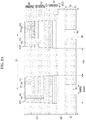
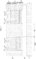
- FIGS. 1A and 1B are top views of a light emitting device according to an exemplary embodiment.
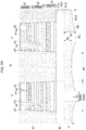
- FIGS. 2A , 2B , 2C , and 2D are cross-sectional views taken along lines A-A' of FIGS. 1A and 1B .
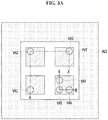
- FIG. 3A is a top view of a light emitting structure of the light emitting device shown in FIG. 1A
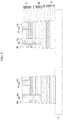
- FIG. 3B is a cross-sectional view taken along lines A-A' and B-B' of FIG. 3A .
- FIG. 1A is a planar view obtained when viewed from the pads of a light emitting device
- FIG. 1B is a planar view obtained when viewed from the light extraction surface of the light emitting device
- FIG. 3A is a planar view obtained when viewed from the pads of the light emitting device.
- a light emitting device may include a substrate 100 having a first surface SF1_S and a second surface SF2_S opposing the first surface SF1_S, a plurality of light emitting parts LE1, LE2, and LE3 disposed on the first surface SF1_S of the substrate 100, and a light shielding layer LS disposed on the second surface SF2_S of the substrate 100.
- the substrate 100 may be capable of growing a gallium nitride-based semiconductor layer thereon, and may include a sapphire (Al 2 O 3 ), a silicon carbide (SiC), a gallium nitride (GaN), an indium gallium nitride (InGaN), an aluminum gallium nitride (AlGaN), an aluminum nitride (AlN), a gallium oxide (Ga 2 O 3 ), or silicon. Also, the substrate 100 may be a patterned sapphire substrate. In some exemplary embodiments, the substrate 100 may include a material that transmits visible light.
- the light emitting device may include light emitting structures LED, in which a first light emitting part LE1, a second light emitting part LE2, and a third light emitting part LE3 are vertically stacked.
- the substrate 100 may include light emitting areas LEA, in which the light emitting structures LED are disposed, and a peripheral area PPA around the light emitting areas LEA.
- each of the light emitting structures LED has a width that gradually increases from the third light emitting part LE3 to the first light emitting part LE1
- each of the light emitting areas LEA may have a first width W1 that is substantially the same as the largest width of each light emitting structure LED.
- the wavelength of light emitted from the first light emitting part LE1 may be the shortest
- the wavelength of light emitted from the second light emitting part LE2 may be longer than the wavelength of light emitted from the first light emitting part LE1 and be shorter than the wavelength of light emitted from the third light emitting part LE3
- the wavelength of light emitted from the third light emitting part LE3 may be longest.
- the first light emitting part LE1 may emit blue light
- the second light emitting part LE2 may emit green light
- the third light emitting part LE3 may emit red light.
- light generated from the first light emitting part LE1 may have a wavelength of about 450 nm to about 495 nm
- light generated from the second light emitting part LE2 may have a wavelength of about 495 nm to about 570 nm
- light generated from the third light emitting part LE3 may have a wavelength of about 620 nm to about 750 nm.
- the inventive concepts are not limited thereto.
- the second light emitting part LE2 may emit light having a shorter wavelength than that emitted from the first light emitting part LE1.
- the first light emitting part LE1 may include a first n-type semiconductor layer 102, a first active layer 104, a first p-type semiconductor layer 106, and a first ohmic layer 108
- the second light emitting part LE2 may include a second n-type semiconductor layer 202, a second active layer 204, a second p-type semiconductor layer 206, and a second ohmic layer 208
- the third light emitting part LE3 may include a third n-type semiconductor layer 302, a third active layer 304, a third p-type semiconductor layer 306, and a third ohmic layer 308.
- Each of the first n-type semiconductor layer 102, the second n-type semiconductor layer 202, and the third n-type semiconductor layer 302 may be a Si-doped gallium nitride-based semiconductor layer.
- Each of the first p-type semiconductor layer 106, the second p-type semiconductor layer 206, and the third p-type semiconductor layer 306 may be a Mg-doped gallium nitride-based semiconductor layer.
- Each of the first active layer 104, the second active layer 204, and the third active layer 304 may include a multi-quantum well (MQW), and the composition ratio thereof may be determined to emit light of a desired peak wavelength.
- MQW multi-quantum well
- a transparent conductive oxide such as tin oxide (SnO), indium oxide (InO 2 ), zinc oxide (ZnO), indium tin oxide (ITO), or indium tin zinc oxide (ITZO) may be used.
- TCO transparent conductive oxide
- SnO tin oxide
- InO 2 indium oxide
- ZnO zinc oxide
- ITO indium tin oxide
- ITZO indium tin zinc oxide
- the first light emitting part LE1 may be spaced apart from the second light emitting part LE2.
- the first ohmic layer 108 of the first light emitting part LE1 and the second ohmic layer 208 of the second light emitting part LE2 may face each other.
- the first ohmic layer 108 of the first light emitting part LE1 and the second n-type semiconductor layer 202 of the second light emitting part LE2 may face each other.
- the second light emitting part LE2 may be spaced apart from the third light emitting part LE3.
- the second n-type semiconductor layer 202 of the second light emitting part LE2 and the third ohmic layer 308 of the third light emitting part LE3 may face each other.
- the second ohmic layer 208 of the second light emitting part LE2 and the third n-type semiconductor layer 302 of the third light emitting part LE3 may face each other.
- the light emitting device may further include a first adhesion part AD1 disposed between the first light emitting part LE1 and the second light emitting part LE2 to bond the first light emitting part LE1 and the second light emitting part LE2, and a second adhesion part AD2 disposed between the second light emitting part LE2 and the third light emitting part LE3 to bond the second light emitting part LE2 and the third light emitting part LE3.
- Each of the first adhesion part AD1 and the second adhesion part AD2 may include a material that transmits visible light and has an insulation property.
- Each of the first adhesion part AD1 and the second adhesion part AD2 may include a polymer, a resist, or a polyimide.
- each of the first adhesion part AD1 and the second adhesion part AD2 may include SOG (spin-on-glass), BCB (benzo cyclo butadiene), HSQ (hydrogen silsesquioxanes), or an SU-8 photoresist.
- SOG spin-on-glass
- BCB benzo cyclo butadiene
- HSQ hydrogen silsesquioxanes
- the light emitting device may further include a first color filter CF1 disposed between the first light emitting part LE1 and the second light emitting part LE2, and a second color filter CF2 disposed between the second light emitting part LE2 and the third light emitting part LE3.
- the first color filter CF1 may be disposed on the first ohmic layer 108 of the first light emitting part LE1 or the second ohmic layer 208 of the second light emitting part LE2.
- the second color filter CF2 may be disposed on the second n-type semiconductor layer 202 of the second light emitting part LE2 or the third ohmic layer 308 of the third light emitting part LE3.
- the first color filter CF1 may reflect light emitted from the first light emitting part LE1 and pass light emitted from the second light emitting part LE2 and the third light emitting part LE3, such that light emitted from the first light emitting part LE1 does not exert an influence on each of the second light emitting part LE2 and the third light emitting part LE3.
- the second color filter CF2 may reflect light emitted from the first light emitting part LE1 and the second light emitting part LE2 and pass light emitted from the third light emitting part LE3, such that light emitted from the first light emitting part LE1 and the second light emitting part LE2 does not exert an influence on the third light emitting part LE3.
- Each of the first color filter CF1 and the second color filter CF2 may include a distributed Bragg reflector (DBR), in which TiO 2 and SiO 2 are alternately stacked.
- the first color filter CF1 may be different from the second color filter CF2 in terms of the alternation number and thickness of TiO2 and SiO2.
- at least one of the first color filter CF1 and the second color filter CF2 may be selectively omitted.
- the light emitting device may further include a first via pattern VA1, which passes through the third light emitting part LE3, the second color filter CF2, the second adhesion part AD2, the second light emitting part LE2, the first adhesion part AD1, and the first color filter CF1 and is brought into electrical contact with the first ohmic layer 108, a second via pattern VA2, which passes through the third light emitting part LE3, the second color filter CF2, the second adhesion part AD2, the second n-type semiconductor layer 202, the second active layer 204, and the second p-type semiconductor layer 206 and is brought into electrical contact with the second ohmic layer 208, and a third via pattern VA3, which passes through the third n-type semiconductor layer 302, the third active layer 304, and the third p-type semiconductor layer 306 and is brought into electrical contact with the third ohmic layer 308.
- a first via pattern VA1 which passes through the third light emitting part LE3, the second color filter CF2, the second adhesion part AD2, the second light
- the light emitting device may further include a fourth via pattern VA4, which passes through the third light emitting part LE3, the second color filter CF2, the second adhesion part AD2, the second light emitting part LE2, the first adhesion part AD1, the first color filter CF1, the first ohmic layer 108, the first p-type semiconductor layer 106, and the first active layer 104 and is brought into electrical contact with the first n-type semiconductor layer 102, a fifth via pattern VA5, which passes through the third light emitting part LE3, the second color filter CF2, and the second adhesion part AD2 and is brought into electrical contact with the second n-type semiconductor layer 202, and a sixth via pattern VA6, which is brought into electrical contact with the third n-type semiconductor layer 302.
- a fourth via pattern VA4 which passes through the third light emitting part LE3, the second color filter CF2, the second adhesion part AD2, the second light emitting part LE2, the first adhesion part AD1, the first color filter CF1, the first ohmic layer 108
- the light emitting device may further include a first pad PD1 electrically coupled with the first ohmic layer 108 through the first via pattern VA1, a second pad PD2 electrically coupled with the second ohmic layer 208 through the second via pattern VA2, a third pad PD3 electrically coupled with the third ohmic layer 308 through the third via pattern VA3, and a common pad CPD electrically coupled in common with the first n-type semiconductor layer 102, the second n-type semiconductor layer 202, and the third n-type semiconductor layer 302 through the fourth, fifth, and sixth via patterns VA4, VA5, and VA6, respectively.
- each of the first pad PD1, the second pad PD2, the third pad PD3, and the common pad CPD may be disposed on the third light emitting part LE3.
- the common pad CPD is illustrated as being coupled in common with the first n-type semiconductor layer 102, the second n-type semiconductor layer 202, and the third n-type semiconductor layer 302, however, the inventive concepts are not limited thereto.
- the common pad CPD may be coupled in common with the first ohmic layer 108, the second ohmic layer 208, and the third ohmic layer 308.
- the light emitting device may further include a passivation layer PVT, which surrounds the outer sidewalls of the first via pattern VA1, the second via pattern VA2, the third via pattern VA3, the fourth via pattern VA4, the fifth via pattern VA5, and the sixth via pattern VA6, and extends onto the third light emitting part LE3.
- a passivation layer PVT which surrounds the outer sidewalls of the first via pattern VA1, the second via pattern VA2, the third via pattern VA3, the fourth via pattern VA4, the fifth via pattern VA5, and the sixth via pattern VA6, and extends onto the third light emitting part LE3.
- the light emitting parts are illustrated as including the first light emitting part LE1, the second light emitting part LE2, and the third light emitting part LE3 that are vertically stacked, and that the light emitting device is illustrated as including the via patterns VA1, VA2, VA3, VA4, VA5, and VA6 passing through the first light emitting part LE1, the second light emitting part LE2, and the third light emitting part LE3, however, the inventive concepts are not limited thereto.
- the light emitting device may have a mesa structure, which exposes the first n-type semiconductor layer 102, the second n-type semiconductor layer 202, the third n-type semiconductor layer 302, the first ohmic layer 108, the second ohmic layer 208, and the third ohmic layer 308.
- the light emitting device may have a structure, in which the first light emitting part LE1, the second light emitting part LE2 and the third light emitting part LE3, are horizontally disposed on the same plane.
- the light shielding layer LS may include a plurality of holes HL, each exposing at least a portion of corresponding light emitting area LEA on the second surface SF2_S of the substrate 100.
- Each of the holes HL of the light shielding layer LS defines the light extraction surface LEX, and light emitted from the light extraction surface LEX may be emitted through the hole HL exposing the light extraction surface LEX. More particularly, each hole HL may function as a light extraction path.
- each light extraction surface LEX in the light emitting area LEA may have a second width W2 less than the first width W1 of the light emitting area LEA.
- the center of the light extraction surface LEX may be substantially the same as the center of the light emitting area LEA.
- the light shielding layer LS may include metal, such as Ti, Ni, Al, Ag, and Cr, or may include a material, such as a photoresist, epoxy, PDMS (polydimethylsiloxane), and a black matrix.
- metal such as Ti, Ni, Al, Ag, and Cr
- a material such as a photoresist, epoxy, PDMS (polydimethylsiloxane), and a black matrix.
- a thickness TH of the light shielding layer LS may be equal to or greater than a length of the longest wavelength among the wavelengths of light generated by the light emitting parts LE1, LE2, and LE3.
- the first light emitting part LE1 emits blue light having the wavelength of about 450 nm to about 495 nm
- the second light emitting part LE2 emits green light having the wavelength of about 495 nm to about 570 nm
- the third light emitting part LE3 emits red light having the wavelength of about 620 nm to about 750 nm
- the thickness TH of the light shielding layer LS may be equal to or greater than the wavelength of light generated from the third light emitting part LE3.
- the second width W2 of the light extraction surface LEX defined by the light shielding layer LS may be less than the thickness TH of the light shielding layer LS.
- the second width W2 may be about 5 ⁇ m.
- the light emitting device may have an improved contrast and color reproducibility.
- the width of the light extraction surface LEX is small, light passed through the light shielding layer LS may be spread by diffraction, which may cause an image displayed by light emitted from the light emitting device may be blurred.
- the light shielding layer LS by forming the light shielding layer LS to have a thickness TH greater than the longest wavelength among the wavelengths of light generated from the light emitting parts LE1, LE2, and LE3, the diffraction of light may be vanished while passing through the light shielding layer LS to suppress blurring of an image displayed.
- the sidewall SW exposed by the hole HL of the light shielding layer LS may be vertical to the substrate 100.
- the light shielding layer LS may have substantially a constant thickness TH.
- the light emitting structures LED will be described with reference to a first light emitting structure LED1 and a second light emitting structure LED2, and the holes HL will be described with reference to a first hole HL1 and a second hole HL2.
- the first light emitting structure LED1 may emit light through the first hole HL1
- the second light emitting structure LED2 may emit light through the second hole HL2.
- Light generated from the first light emitting structure LED1, which is reflected and radiated to the second hole HL2 may have a decreased intensity as a portion of light may be vanished while passing through the substrate 100, and while passing through the thick light shielding layer LS towards the second hole HL2. Also, even when light generated from the first light emitting structure LED1 is emitted through the first hole HL1, a diffraction phenomenon may be vanished while light passes through the thick light shielding layer LS.
- the sidewall SW exposed by the hole HL of the light shielding layer LS may be vertical with respect to a longitudinal direction of the substrate 100, and include a rough surface RGH.
- the rough surface RGH may include a concave and convex pattern CC.
- light generated from the first light emitting structure LED1 may be vanished while passing through the thick light shielding layer LS towards the second hole HL2.
- the sidewall SW of the second hole HL2 is formed with the rough surface RGH, light generated from the first light emitting structure LED1 may be quickly and completely vanished as being diffusively reflected and scattered.
- the sidewall SW exposed by the hole HL of the light shielding layer LS may have a slope.
- the light shielding layer LS includes the first surface SF1_LS facing the second surface SF2_S of the substrate 100, and the second surface SF2_LS opposing the first surface SF1_LS, and the light shielding layer LS may have a width that gradually decreases from the second surface SF2_LS to the first surface SF1_LS of the light shielding layer LS.
- the sidewall SW of the light shielding layer LS may have a reverse slope. The area of the sidewall SW having the reverse slope may be greater than the area of the sidewall SW that is vertical.
- light generated from the first light emitting structure LED1 may be vanished by the thick light shielding layer LS while passing through the second hole HL2. Since the sidewall SW of the second hole HL2 according to the illustrated exemplary embodiment has a sidewall which has a reverse slope, light radiated from various angles may be efficiently reflected and absorbed to be efficiently be vanished.
- the light shielding layer LS includes the first surface SF1_LS facing the second surface SF2_S of the substrate 100, and the second surface SF2_LS opposing the first surface SF1_LS and having a concaved surface CVS. More particularly, the light shielding layer LS may have a thickness TH that gradually decreases from one end of the light shielding layer LS towards a center thereof. For example, one end (or an edge) of the light shielding layer LS may have a first thickness TH1, and the center of the light shielding layer LS may have a second thickness TH2 less than the first thickness TH.
- the hole HL may have a longer depth, which may efficiently vanish light emitted from a neighboring light emitting structure LED as described above. Furthermore, since the center of the light shielding layer LS has a relatively thin thickness TH2, a tension to be applied to the light emitting device may be reduced, thereby preventing or at least suppressing the breakage of the light emitting device.
- FIGS. 4 to 8 cross-sectional views illustrating a method for manufacturing a light emitting device according to an exemplary embodiment.
- a first light emitting part LE1, a second light emitting part LE2, and a third light emitting part LE3 may be sequentially stacked on a first surface of a first substrate 100.
- the first substrate 100 may be a growth substrate capable of growing the first light emitting part LE1 thereon, and a transfer substrate for mounting the first light emitting part LE1 to a target apparatus.
- a completed light emitting device is applied to a display device, such as a wristwatch
- the first substrate 100 may be cut to a size that corresponds to a display unit of the wristwatch, and then, the first light emitting part LE1 may be grown thereon.
- a first n-type semiconductor layer 102, a first active layer 104, and a first p-type semiconductor layer 106 may be sequentially formed on the first substrate 100 by using a growing method, such as MOCVD (metal organic chemical vapor deposition), MBE (molecular beam epitaxy), HVPE (hydride vapor phase epitaxy), and MOC (metal-organic chloride).
- MOCVD metal organic chemical vapor deposition
- MBE molecular beam epitaxy
- HVPE hydrogen vapor phase epitaxy
- MOC metal-organic chloride
- a first ohmic layer 108 may be formed on the first p-type semiconductor layer 106 through a chemical vapor deposition (CVD) process, a physical vapor deposition (PVD), etc., to form the first light emitting part LE1.
- CVD chemical vapor deposition
- PVD physical vapor deposition
- a second n-type semiconductor layer 202, a second active layer 204, and a second p-type semiconductor layer 206 may be sequentially formed on a second substrate by using a growing method, such as MOCVD, MBE, HVPE, and MOC.
- a second ohmic layer 208 may be formed on the second p-type semiconductor layer 206 through a CVD process, a PVD process, etc., to form the second light emitting part LE2.
- the second ohmic layer 208 may be disposed to face the first ohmic layer 108, and the second light emitting part LE2 may be bonded to the first light emitting part LE1 through a first adhesion part AD1.
- the second substrate may be removed through a laser lift-off (LLO) process or a chemical lift-off (CLO) process.
- LLO laser lift-off
- CLO chemical lift-off
- a third n-type semiconductor layer 302, a third active layer 304, and a third p-type semiconductor layer 306 may be sequentially formed on a third substrate by using a growing method, such as MOCVD, MBE, HVPE, and MOC.
- a third ohmic layer 308 may be formed on the third p-type semiconductor layer 306 through a CVD process, a PVD process, etc., to form the third light emitting part LE3.
- the third substrate may be turned over, such that the second n-type semiconductor layer 202 of the second light emitting part LE2 and the third ohmic layer 308 of the third light emitting part LE3 face each other, and the second light emitting part LE2 and the third light emitting part LE3 may be bonded to each other through a second adhesion part AD2. After bonding the second light emitting part LE2 and the third light emitting part LE3 by the second adhesion part AD2, the third substrate may be removed through an LLO or CLO process.
- a first via hole exposing the first ohmic layer 108, a second via hole exposing the second ohmic layer 208, a third via hole exposing the third ohmic layer 308, a fourth via hole exposing the first n-type semiconductor layer 102, a fifth via hole exposing the second n-type semiconductor layer 202, and a sixth via hole exposing the third n-type semiconductor layer 302 may be formed.
- a plurality of light emitting structures LED may be isolated on the first surface of the first substrate 100.
- a passivation layer PVT may be formed in at least a portion of the first via hole, the second via hole, the third via hole, the fourth via hole, the fifth via hole, and the sixth via hole, and to extend to the top surface of the third n-type semiconductor layer 302.
- the first ohmic layer 108 may be exposed at the bottom surface of the first via hole
- the second ohmic layer 208 may be exposed at the bottom surface of the second via hole
- the third ohmic layer 308 may be exposed at the bottom surface of the third via hole
- the first n-type semiconductor layer 102 may be exposed at the bottom surface of the fourth via hole
- the second n-type semiconductor layer 202 may be exposed at the bottom surface of the fifth via hole
- the third n-type semiconductor layer 302 may be exposed at the bottom surface of the sixth ohmic layer.
- a first via pattern VA1, a second via pattern VA2, a third via pattern VA3, a fourth via pattern VA4, a fifth via pattern VA5, and a sixth via pattern VA6 may be disposed in the first via hole, the second via hole, the third via hole, the fourth via hole, the fifth via hole, and the sixth via hole, respectively, along with the passivation layer PVT.
- a first pad PD1 may be formed on the first via pattern VA1
- a second pad PD2 may be formed on the second via pattern VA2
- a third pad PD3 may be formed on the third via pattern VA3
- a common pad CPD may be formed to be electrically coupled in common with the fourth via pattern VA4, the fifth via pattern VA5, and the sixth via pattern VA6.
- an additional light shielding layer ALS may be disposed on the first surface of the first substrate 100 between the light emitting structures LED.
- a peripheral area PPA around the light emitting areas LEA, in which the light emitting structures LED are formed, may be covered by the additional light shielding layer ALS.
- a light shielding layer LS may be formed on a second surface of the first substrate 100.
- the light shielding layer LS may have a thickness TH that is greater than the wavelength of the light generated from the third light emitting part LE3.
- each hole HL may function as a light extraction path, through which light from each of the light emitting structures LED is emitted.
- each hole HL may be formed within each light emitting area LEA, and the center of each hole HL may be substantially the same as the center of each light emitting area LEA.
- a sidewall SW of the light shielding layer LS exposed by each hole HL may be vertical with respect to the substrate 100.
- the mask pattern may be selected, such that the sidewall SW of the light shielding layer LS is vertically etched.
- a rough surface RGH may be formed by an etching process, such as wet etching, for example.
- a sidewall SW of the light shielding layer LS exposed by each hole HL may have a reverse slope.
- the mask pattern may be selected, such that the sidewall SW of the light shielding layer LS is etched to have a reversely sloped surface.
- the light shielding layer LS when the light shielding layer LS has a first surface SF1_LS facing a second surface SF2_S of the substrate 100, and a second surface SF2_LS opposing the first surface SF1_LS, a concave may be formed on the second surface SF2_LS of the light shielding layer LS through a CMP process or the like. More particularly, the light shielding layer LS may have a thickness TH that gradually decreases from an edge to the center of the light shielding layer LS.
- a light emitting device including the light emitting structures LED, the light shielding layer LS, and the additional light shielding layer ALS may be formed on the first substrate 100. Since the first substrate 100 may be cut to a size that corresponds to the display unit of a target mounting apparatus, for example, the processes of cutting, transferring, and mounting the light emitting structures LED formed on the first substrate 100 may be obviated, and the first substrate 100 may be directly mounted to the target apparatus. In this manner, a light emitting device according to an exemplary embodiment may be easily be mounted to the target apparatus, while obviating the need of separate cutting, transferring, and/or mounting process, which otherwise would increase the manufacturing costs and complexity, especially when the size of a light emitting device is small.
Landscapes
- Led Devices (AREA)
- Led Device Packages (AREA)
Abstract
Description
- Exemplary embodiments of the invention relate generally to a light emitting device, and more specifically, to a light emitting device including a plurality of light emitting parts.
- Light emitting diodes, as inorganic light sources, are being diversely used in various fields, such as display devices, vehicle lamps, and general lighting. Light emitting diodes are rapidly replacing existing light sources due to their longer lifetime, lower power consumption, and faster response speed than existing light sources.
- In general, a display device displays various colors by utilizing mixed colors of blue, green, and red. Each pixel of a display device includes blue, green, and red sub-pixels, the color of a particular pixel is determined through the colors of these sub-pixels, and an image is displayed by a combination of pixels.
- Light emitting diodes have been mainly used as backlight sources in display devices. However, recently, a micro LED display has been developed as a next generation display, which may directly display images by using light emitting diodes.
- Devices constructed according to exemplary embodiments of the invention are capable of suppressing color mixing and improving light reproducibility.
- Additional features of the inventive concepts will be set forth in the description which follows, and in part will be apparent from the description, or may be learned by practice of the inventive concepts.
- A light emitting device according to an exemplary embodiment includes a substrate having a first surface and a second surface opposing each other, a plurality of light emitting parts disposed on the first surface of the substrate and defining a light emitting area, and a light shielding layer disposed on the second surface of the substrate and exposing at least a portion of the light emitting area, in which the light shielding layer has a thickness greater than a length of the longest wavelength among wavelengths of light generated from the light emitting parts.
- The light shielding layer may define a light extraction surface by covering peripheries of the light emitting parts.
- A width of the light extraction surface may be less than the thickness of the light shielding layer.
- The light shielding layer may have a side surface including a rough surface.
- The light shielding layer may include a first surface facing the second surface of the substrate and a second surface opposing the first surface thereof, and the second surface of the light shielding layer may have a concaved surface.
- The light shielding layer may have a sidewall that is vertical with respect to a longitudinal direction of the substrate.
- The light shielding layer may have an inclined sidewall with respect to a longitudinal direction of the substrate.
- The light shielding layer may have a first surface facing the second surface of the substrate and a second surface opposing the first surface thereof, and the light shielding layer may have a width that increases from the first surface of the light shielding layer to the second surface of the light shielding layer.
- The details of other embodiments are included in the detailed description and the drawings.
- In the light emitting device according to the embodiments of the disclosure, since a light extraction surface smaller than a light emitting area is defined by using a light shielding layer, the contrast of the light emitting device may be improved. Also, by vanishing the diffraction of the light emitted through the light extraction surface of a narrow width by using the light shielding layer of a sufficient thickness, the image blurring of a display device using the light emitting device may be prevented.
-
-
FIGS. 1A and1B are top views of a light emitting device according to an exemplary embodiment. -
FIGS. 2A ,2B ,2C , and2D are cross-sectional views taken along lines A-A' ofFIGS. 1A and1B according to exemplary embodiments. -
FIG. 3A is a top view of a light emitting structure of the light emitting device ofFIG. 1A . -
FIG. 3B is a cross-sectional view taken along lines A-A' and B-B' ofFIG. 3A . -
FIGS. 4 ,5 ,6 ,7 , and8 are cross-sectional views illustrating a method for manufacturing a light emitting device according to an exemplary embodiment. - In order to understand the configuration and effect of the disclosure sufficiently, embodiments of the disclosure will be described with reference to the accompanying drawings. However, the disclosure is not limited to the embodiments set forth herein and may be implemented in various forms, and a variety of changes may be added.
- As used in the embodiments of the disclosure, a technical term may be interpreted as a meaning conventionally known to those of ordinary skill in the art unless defined otherwise.
- Hereinafter, a light emitting device will be described below with reference to the accompanying drawings through various examples of embodiments.
-
FIGS. 1A and1B are top views of a light emitting device according to an exemplary embodiment.FIGS. 2A ,2B ,2C , and2D are cross-sectional views taken along lines A-A' ofFIGS. 1A and1B .FIG. 3A is a top view of a light emitting structure of the light emitting device shown inFIG. 1A , andFIG. 3B is a cross-sectional view taken along lines A-A' and B-B' ofFIG. 3A . -
FIG. 1A is a planar view obtained when viewed from the pads of a light emitting device, andFIG. 1B is a planar view obtained when viewed from the light extraction surface of the light emitting device.FIG. 3A is a planar view obtained when viewed from the pads of the light emitting device. - Referring to
FIGS. 1A ,1B ,2A ,2B ,2C , and2D , a light emitting device may include asubstrate 100 having a first surface SF1_S and a second surface SF2_S opposing the first surface SF1_S, a plurality of light emitting parts LE1, LE2, and LE3 disposed on the first surface SF1_S of thesubstrate 100, and a light shielding layer LS disposed on the second surface SF2_S of thesubstrate 100. - The
substrate 100 may be capable of growing a gallium nitride-based semiconductor layer thereon, and may include a sapphire (Al2O3), a silicon carbide (SiC), a gallium nitride (GaN), an indium gallium nitride (InGaN), an aluminum gallium nitride (AlGaN), an aluminum nitride (AlN), a gallium oxide (Ga2O3), or silicon. Also, thesubstrate 100 may be a patterned sapphire substrate. In some exemplary embodiments, thesubstrate 100 may include a material that transmits visible light. - Referring to
FIGS. 3A and3B , the light emitting device may include light emitting structures LED, in which a first light emitting part LE1, a second light emitting part LE2, and a third light emitting part LE3 are vertically stacked. Thesubstrate 100 may include light emitting areas LEA, in which the light emitting structures LED are disposed, and a peripheral area PPA around the light emitting areas LEA. For example, when each of the light emitting structures LED has a width that gradually increases from the third light emitting part LE3 to the first light emitting part LE1, each of the light emitting areas LEA may have a first width W1 that is substantially the same as the largest width of each light emitting structure LED. - When the second surface SF2_S of the
substrate 100 includes a light extraction surface LEX, the wavelength of light emitted from the first light emitting part LE1 may be the shortest, the wavelength of light emitted from the second light emitting part LE2 may be longer than the wavelength of light emitted from the first light emitting part LE1 and be shorter than the wavelength of light emitted from the third light emitting part LE3, and the wavelength of light emitted from the third light emitting part LE3 may be longest. For example, the first light emitting part LE1 may emit blue light, the second light emitting part LE2 may emit green light, and the third light emitting part LE3 may emit red light. In this case, light generated from the first light emitting part LE1 may have a wavelength of about 450 nm to about 495 nm, light generated from the second light emitting part LE2 may have a wavelength of about 495 nm to about 570 nm, and light generated from the third light emitting part LE3 may have a wavelength of about 620 nm to about 750 nm. However, the inventive concepts are not limited thereto. For example, in some exemplary embodiments, the second light emitting part LE2 may emit light having a shorter wavelength than that emitted from the first light emitting part LE1. - The first light emitting part LE1 may include a first n-
type semiconductor layer 102, a firstactive layer 104, a first p-type semiconductor layer 106, and a firstohmic layer 108, the second light emitting part LE2 may include a second n-type semiconductor layer 202, a secondactive layer 204, a second p-type semiconductor layer 206, and a secondohmic layer 208, and the third light emitting part LE3 may include a third n-type semiconductor layer 302, a thirdactive layer 304, a third p-type semiconductor layer 306, and a thirdohmic layer 308. - Each of the first n-
type semiconductor layer 102, the second n-type semiconductor layer 202, and the third n-type semiconductor layer 302 may be a Si-doped gallium nitride-based semiconductor layer. Each of the first p-type semiconductor layer 106, the second p-type semiconductor layer 206, and the third p-type semiconductor layer 306 may be a Mg-doped gallium nitride-based semiconductor layer. Each of the firstactive layer 104, the secondactive layer 204, and the thirdactive layer 304 may include a multi-quantum well (MQW), and the composition ratio thereof may be determined to emit light of a desired peak wavelength. As each of the firstohmic layer 108, the secondohmic layer 208 and the thirdohmic layer 308, a transparent conductive oxide (TCO), such as tin oxide (SnO), indium oxide (InO2), zinc oxide (ZnO), indium tin oxide (ITO), or indium tin zinc oxide (ITZO) may be used. - The first light emitting part LE1 may be spaced apart from the second light emitting part LE2. For example, the first
ohmic layer 108 of the first light emitting part LE1 and the secondohmic layer 208 of the second light emitting part LE2 may face each other. As another example, the firstohmic layer 108 of the first light emitting part LE1 and the second n-type semiconductor layer 202 of the second light emitting part LE2 may face each other. - The second light emitting part LE2 may be spaced apart from the third light emitting part LE3. For example, the second n-
type semiconductor layer 202 of the second light emitting part LE2 and the thirdohmic layer 308 of the third light emitting part LE3 may face each other. As another example the secondohmic layer 208 of the second light emitting part LE2 and the third n-type semiconductor layer 302 of the third light emitting part LE3 may face each other. - The light emitting device may further include a first adhesion part AD1 disposed between the first light emitting part LE1 and the second light emitting part LE2 to bond the first light emitting part LE1 and the second light emitting part LE2, and a second adhesion part AD2 disposed between the second light emitting part LE2 and the third light emitting part LE3 to bond the second light emitting part LE2 and the third light emitting part LE3. Each of the first adhesion part AD1 and the second adhesion part AD2 may include a material that transmits visible light and has an insulation property. Each of the first adhesion part AD1 and the second adhesion part AD2 may include a polymer, a resist, or a polyimide. For example, each of the first adhesion part AD1 and the second adhesion part AD2 may include SOG (spin-on-glass), BCB (benzo cyclo butadiene), HSQ (hydrogen silsesquioxanes), or an SU-8 photoresist.
- The light emitting device may further include a first color filter CF1 disposed between the first light emitting part LE1 and the second light emitting part LE2, and a second color filter CF2 disposed between the second light emitting part LE2 and the third light emitting part LE3. The first color filter CF1 may be disposed on the first
ohmic layer 108 of the first light emitting part LE1 or the secondohmic layer 208 of the second light emitting part LE2. The second color filter CF2 may be disposed on the second n-type semiconductor layer 202 of the second light emitting part LE2 or the thirdohmic layer 308 of the third light emitting part LE3. The first color filter CF1 may reflect light emitted from the first light emitting part LE1 and pass light emitted from the second light emitting part LE2 and the third light emitting part LE3, such that light emitted from the first light emitting part LE1 does not exert an influence on each of the second light emitting part LE2 and the third light emitting part LE3. The second color filter CF2 may reflect light emitted from the first light emitting part LE1 and the second light emitting part LE2 and pass light emitted from the third light emitting part LE3, such that light emitted from the first light emitting part LE1 and the second light emitting part LE2 does not exert an influence on the third light emitting part LE3. Each of the first color filter CF1 and the second color filter CF2 may include a distributed Bragg reflector (DBR), in which TiO2 and SiO2 are alternately stacked. The first color filter CF1 may be different from the second color filter CF2 in terms of the alternation number and thickness of TiO2 and SiO2. In some exemplary embodiments, at least one of the first color filter CF1 and the second color filter CF2 may be selectively omitted. - The light emitting device may further include a first via pattern VA1, which passes through the third light emitting part LE3, the second color filter CF2, the second adhesion part AD2, the second light emitting part LE2, the first adhesion part AD1, and the first color filter CF1 and is brought into electrical contact with the first
ohmic layer 108, a second via pattern VA2, which passes through the third light emitting part LE3, the second color filter CF2, the second adhesion part AD2, the second n-type semiconductor layer 202, the secondactive layer 204, and the second p-type semiconductor layer 206 and is brought into electrical contact with the secondohmic layer 208, and a third via pattern VA3, which passes through the third n-type semiconductor layer 302, the thirdactive layer 304, and the third p-type semiconductor layer 306 and is brought into electrical contact with the thirdohmic layer 308. Also, the light emitting device may further include a fourth via pattern VA4, which passes through the third light emitting part LE3, the second color filter CF2, the second adhesion part AD2, the second light emitting part LE2, the first adhesion part AD1, the first color filter CF1, the firstohmic layer 108, the first p-type semiconductor layer 106, and the firstactive layer 104 and is brought into electrical contact with the first n-type semiconductor layer 102, a fifth via pattern VA5, which passes through the third light emitting part LE3, the second color filter CF2, and the second adhesion part AD2 and is brought into electrical contact with the second n-type semiconductor layer 202, and a sixth via pattern VA6, which is brought into electrical contact with the third n-type semiconductor layer 302. - The light emitting device may further include a first pad PD1 electrically coupled with the first
ohmic layer 108 through the first via pattern VA1, a second pad PD2 electrically coupled with the secondohmic layer 208 through the second via pattern VA2, a third pad PD3 electrically coupled with the thirdohmic layer 308 through the third via pattern VA3, and a common pad CPD electrically coupled in common with the first n-type semiconductor layer 102, the second n-type semiconductor layer 202, and the third n-type semiconductor layer 302 through the fourth, fifth, and sixth via patterns VA4, VA5, and VA6, respectively. According to an exemplary embodiment, each of the first pad PD1, the second pad PD2, the third pad PD3, and the common pad CPD may be disposed on the third light emitting part LE3. - While the common pad CPD is illustrated as being coupled in common with the first n-
type semiconductor layer 102, the second n-type semiconductor layer 202, and the third n-type semiconductor layer 302, however, the inventive concepts are not limited thereto. For example, in some exemplary embodiments, the common pad CPD may be coupled in common with the firstohmic layer 108, the secondohmic layer 208, and the thirdohmic layer 308. - The light emitting device may further include a passivation layer PVT, which surrounds the outer sidewalls of the first via pattern VA1, the second via pattern VA2, the third via pattern VA3, the fourth via pattern VA4, the fifth via pattern VA5, and the sixth via pattern VA6, and extends onto the third light emitting part LE3.
- While the light emitting parts are illustrated as including the first light emitting part LE1, the second light emitting part LE2, and the third light emitting part LE3 that are vertically stacked, and that the light emitting device is illustrated as including the via patterns VA1, VA2, VA3, VA4, VA5, and VA6 passing through the first light emitting part LE1, the second light emitting part LE2, and the third light emitting part LE3, however, the inventive concepts are not limited thereto. For example, according to another exemplary embodiment, by etching the vertically stacked first light emitting part LE1, second light emitting part LE2, and third light emitting part LE3, the light emitting device may have a mesa structure, which exposes the first n-
type semiconductor layer 102, the second n-type semiconductor layer 202, the third n-type semiconductor layer 302, the firstohmic layer 108, the secondohmic layer 208, and the thirdohmic layer 308. Moreover, in some exemplary embodiments, the light emitting device may have a structure, in which the first light emitting part LE1, the second light emitting part LE2 and the third light emitting part LE3, are horizontally disposed on the same plane. - Referring to
FIGS. 1A ,1B ,2A ,2B ,2C , and2D , the light shielding layer LS may include a plurality of holes HL, each exposing at least a portion of corresponding light emitting area LEA on the second surface SF2_S of thesubstrate 100. Each of the holes HL of the light shielding layer LS defines the light extraction surface LEX, and light emitted from the light extraction surface LEX may be emitted through the hole HL exposing the light extraction surface LEX. More particularly, each hole HL may function as a light extraction path. - According to an exemplary embodiment, each light extraction surface LEX in the light emitting area LEA may have a second width W2 less than the first width W1 of the light emitting area LEA. The center of the light extraction surface LEX may be substantially the same as the center of the light emitting area LEA.
- The light shielding layer LS may include metal, such as Ti, Ni, Al, Ag, and Cr, or may include a material, such as a photoresist, epoxy, PDMS (polydimethylsiloxane), and a black matrix.
- According to an exemplary embodiment, a thickness TH of the light shielding layer LS may be equal to or greater than a length of the longest wavelength among the wavelengths of light generated by the light emitting parts LE1, LE2, and LE3. For example, when the first light emitting part LE1 emits blue light having the wavelength of about 450 nm to about 495 nm, the second light emitting part LE2 emits green light having the wavelength of about 495 nm to about 570 nm, and the third light emitting part LE3 emits red light having the wavelength of about 620 nm to about 750 nm, the thickness TH of the light shielding layer LS may be equal to or greater than the wavelength of light generated from the third light emitting part LE3.
- According to an exemplary embodiment, the second width W2 of the light extraction surface LEX defined by the light shielding layer LS may be less than the thickness TH of the light shielding layer LS. For example, when a distance DT between the centers of adjacent light emitting structures LED is about 80 µm, the second width W2 may be about 5 µm.
- By defining the light extraction surface LEX to be smaller than the light emitting area LEA by using the light shielding layer LS, the light emitting device may have an improved contrast and color reproducibility.
- In this case, since the width of the light extraction surface LEX is small, light passed through the light shielding layer LS may be spread by diffraction, which may cause an image displayed by light emitted from the light emitting device may be blurred. As such, by forming the light shielding layer LS to have a thickness TH greater than the longest wavelength among the wavelengths of light generated from the light emitting parts LE1, LE2, and LE3, the diffraction of light may be vanished while passing through the light shielding layer LS to suppress blurring of an image displayed.
- Referring to
FIG. 2A , the sidewall SW exposed by the hole HL of the light shielding layer LS according to the illustrated exemplary embodiment may be vertical to thesubstrate 100. The light shielding layer LS may have substantially a constant thickness TH. - Hereinbelow, the light emitting structures LED will be described with reference to a first light emitting structure LED1 and a second light emitting structure LED2, and the holes HL will be described with reference to a first hole HL1 and a second hole HL2. The first light emitting structure LED1 may emit light through the first hole HL1, and the second light emitting structure LED2 may emit light through the second hole HL2.
- While light generated from the first light emitting structure LED1 should be emitted through the first hole HL1, a fraction of light may be reflected and radiated to the neighboring second hole HL2 by using the
substrate 100 as a light guide path. Light generated from the first light emitting structure LED1, which is reflected and radiated to the second hole HL2, may have a decreased intensity as a portion of light may be vanished while passing through thesubstrate 100, and while passing through the thick light shielding layer LS towards the second hole HL2. Also, even when light generated from the first light emitting structure LED1 is emitted through the first hole HL1, a diffraction phenomenon may be vanished while light passes through the thick light shielding layer LS. - Referring to
FIG. 2B , the sidewall SW exposed by the hole HL of the light shielding layer LS according to another exemplary embodiment may be vertical with respect to a longitudinal direction of thesubstrate 100, and include a rough surface RGH. The rough surface RGH may include a concave and convex pattern CC. - As described above, light generated from the first light emitting structure LED1 may be vanished while passing through the thick light shielding layer LS towards the second hole HL2. According to an exemplary embodiment, since the sidewall SW of the second hole HL2 is formed with the rough surface RGH, light generated from the first light emitting structure LED1 may be quickly and completely vanished as being diffusively reflected and scattered.
- Referring to
FIG. 2C , the sidewall SW exposed by the hole HL of the light shielding layer LS may have a slope. For example, the light shielding layer LS includes the first surface SF1_LS facing the second surface SF2_S of thesubstrate 100, and the second surface SF2_LS opposing the first surface SF1_LS, and the light shielding layer LS may have a width that gradually decreases from the second surface SF2_LS to the first surface SF1_LS of the light shielding layer LS. In particular, the sidewall SW of the light shielding layer LS may have a reverse slope. The area of the sidewall SW having the reverse slope may be greater than the area of the sidewall SW that is vertical. - As described above, light generated from the first light emitting structure LED1 may be vanished by the thick light shielding layer LS while passing through the second hole HL2. Since the sidewall SW of the second hole HL2 according to the illustrated exemplary embodiment has a sidewall which has a reverse slope, light radiated from various angles may be efficiently reflected and absorbed to be efficiently be vanished.
- Referring to
FIG. 2D , the light shielding layer LS includes the first surface SF1_LS facing the second surface SF2_S of thesubstrate 100, and the second surface SF2_LS opposing the first surface SF1_LS and having a concaved surface CVS. More particularly, the light shielding layer LS may have a thickness TH that gradually decreases from one end of the light shielding layer LS towards a center thereof. For example, one end (or an edge) of the light shielding layer LS may have a first thickness TH1, and the center of the light shielding layer LS may have a second thickness TH2 less than the first thickness TH. In this manner, since the thickness TH1 of the edge of the light shielding layer LS exposed by the hole HL may be relatively thick, the hole HL may have a longer depth, which may efficiently vanish light emitted from a neighboring light emitting structure LED as described above. Furthermore, since the center of the light shielding layer LS has a relatively thin thickness TH2, a tension to be applied to the light emitting device may be reduced, thereby preventing or at least suppressing the breakage of the light emitting device. - Hereinafter, a method for manufacturing a light emitting device according to an exemplary embodiment will be described. In the illustrated exemplary embodiment, the light emitting device will be described with reference to that shown in
FIGS. 1A ,1B , and2A . -
FIGS. 4 to 8 cross-sectional views illustrating a method for manufacturing a light emitting device according to an exemplary embodiment. - Referring to
FIG. 4 , a first light emitting part LE1, a second light emitting part LE2, and a third light emitting part LE3 may be sequentially stacked on a first surface of afirst substrate 100. - According to an exemplary embodiment, the
first substrate 100 may be a growth substrate capable of growing the first light emitting part LE1 thereon, and a transfer substrate for mounting the first light emitting part LE1 to a target apparatus. For example, when a completed light emitting device is applied to a display device, such as a wristwatch, thefirst substrate 100 may be cut to a size that corresponds to a display unit of the wristwatch, and then, the first light emitting part LE1 may be grown thereon. - A first n-
type semiconductor layer 102, a firstactive layer 104, and a first p-type semiconductor layer 106 may be sequentially formed on thefirst substrate 100 by using a growing method, such as MOCVD (metal organic chemical vapor deposition), MBE (molecular beam epitaxy), HVPE (hydride vapor phase epitaxy), and MOC (metal-organic chloride). A firstohmic layer 108 may be formed on the first p-type semiconductor layer 106 through a chemical vapor deposition (CVD) process, a physical vapor deposition (PVD), etc., to form the first light emitting part LE1. - A second n-
type semiconductor layer 202, a secondactive layer 204, and a second p-type semiconductor layer 206 may be sequentially formed on a second substrate by using a growing method, such as MOCVD, MBE, HVPE, and MOC. A secondohmic layer 208 may be formed on the second p-type semiconductor layer 206 through a CVD process, a PVD process, etc., to form the second light emitting part LE2. - By turning over the second substrate, the second
ohmic layer 208 may be disposed to face the firstohmic layer 108, and the second light emitting part LE2 may be bonded to the first light emitting part LE1 through a first adhesion part AD1. After bonding the first light emitting part LE1 and the second light emitting part LE2, the second substrate may be removed through a laser lift-off (LLO) process or a chemical lift-off (CLO) process. - A third n-
type semiconductor layer 302, a thirdactive layer 304, and a third p-type semiconductor layer 306 may be sequentially formed on a third substrate by using a growing method, such as MOCVD, MBE, HVPE, and MOC. A thirdohmic layer 308 may be formed on the third p-type semiconductor layer 306 through a CVD process, a PVD process, etc., to form the third light emitting part LE3. - The third substrate may be turned over, such that the second n-
type semiconductor layer 202 of the second light emitting part LE2 and the thirdohmic layer 308 of the third light emitting part LE3 face each other, and the second light emitting part LE2 and the third light emitting part LE3 may be bonded to each other through a second adhesion part AD2. After bonding the second light emitting part LE2 and the third light emitting part LE3 by the second adhesion part AD2, the third substrate may be removed through an LLO or CLO process. - Referring to
FIGS. 3B and5 , by etching the third light emitting part LE3, the second light emitting part LE2, and the first light emitting part LE1, a first via hole exposing the firstohmic layer 108, a second via hole exposing the secondohmic layer 208, a third via hole exposing the thirdohmic layer 308, a fourth via hole exposing the first n-type semiconductor layer 102, a fifth via hole exposing the second n-type semiconductor layer 202, and a sixth via hole exposing the third n-type semiconductor layer 302 may be formed. - According to an exemplary embodiment, while forming the first via hole, the second via hole, the third via hole, the fourth via hole, the fifth via hole, and the sixth via hole, by etching the first light emitting part LE1, the second light emitting part LE2, and the third light emitting part LE3, a plurality of light emitting structures LED may be isolated on the first surface of the
first substrate 100. - A passivation layer PVT may be formed in at least a portion of the first via hole, the second via hole, the third via hole, the fourth via hole, the fifth via hole, and the sixth via hole, and to extend to the top surface of the third n-
type semiconductor layer 302. - By etching the passivation layer PVT, the first
ohmic layer 108 may be exposed at the bottom surface of the first via hole, the secondohmic layer 208 may be exposed at the bottom surface of the second via hole, the thirdohmic layer 308 may be exposed at the bottom surface of the third via hole, the first n-type semiconductor layer 102 may be exposed at the bottom surface of the fourth via hole, the second n-type semiconductor layer 202 may be exposed at the bottom surface of the fifth via hole, and the third n-type semiconductor layer 302 may be exposed at the bottom surface of the sixth ohmic layer. - A first via pattern VA1, a second via pattern VA2, a third via pattern VA3, a fourth via pattern VA4, a fifth via pattern VA5, and a sixth via pattern VA6 may be disposed in the first via hole, the second via hole, the third via hole, the fourth via hole, the fifth via hole, and the sixth via hole, respectively, along with the passivation layer PVT.
- A first pad PD1 may be formed on the first via pattern VA1, a second pad PD2 may be formed on the second via pattern VA2, a third pad PD3 may be formed on the third via pattern VA3, and a common pad CPD may be formed to be electrically coupled in common with the fourth via pattern VA4, the fifth via pattern VA5, and the sixth via pattern VA6.
- Referring to
FIG. 6 , an additional light shielding layer ALS may be disposed on the first surface of thefirst substrate 100 between the light emitting structures LED. A peripheral area PPA around the light emitting areas LEA, in which the light emitting structures LED are formed, may be covered by the additional light shielding layer ALS. - Referring to
FIG. 7 , a light shielding layer LS may be formed on a second surface of thefirst substrate 100. According to an exemplary embodiment, the light shielding layer LS may have a thickness TH that is greater than the wavelength of the light generated from the third light emitting part LE3. - Referring to
FIG. 8 , by forming a mask pattern on the light shielding layer LS and etching the light shielding layer LS through using the mask pattern as an etch mask, holes HL each exposing at least a portion of each of the light emitting areas LEA may be formed. Each of the holes HL may function as a light extraction path, through which light from each of the light emitting structures LED is emitted. According to an exemplary embodiment, each hole HL may be formed within each light emitting area LEA, and the center of each hole HL may be substantially the same as the center of each light emitting area LEA. - Referring back to
FIG. 2A , a sidewall SW of the light shielding layer LS exposed by each hole HL may be vertical with respect to thesubstrate 100. The mask pattern may be selected, such that the sidewall SW of the light shielding layer LS is vertically etched. - Referring back to
FIG. 2B , by etching a sidewall SW of the light shielding layer LS that is vertical through using a mask pattern as an etch mask, a rough surface RGH may be formed by an etching process, such as wet etching, for example. - Referring back to
FIG. 2C , a sidewall SW of the light shielding layer LS exposed by each hole HL may have a reverse slope. The mask pattern may be selected, such that the sidewall SW of the light shielding layer LS is etched to have a reversely sloped surface. - Referring back to
FIG. 2D , when the light shielding layer LS has a first surface SF1_LS facing a second surface SF2_S of thesubstrate 100, and a second surface SF2_LS opposing the first surface SF1_LS, a concave may be formed on the second surface SF2_LS of the light shielding layer LS through a CMP process or the like. More particularly, the light shielding layer LS may have a thickness TH that gradually decreases from an edge to the center of the light shielding layer LS. - As such, a light emitting device including the light emitting structures LED, the light shielding layer LS, and the additional light shielding layer ALS may be formed on the
first substrate 100. Since thefirst substrate 100 may be cut to a size that corresponds to the display unit of a target mounting apparatus, for example, the processes of cutting, transferring, and mounting the light emitting structures LED formed on thefirst substrate 100 may be obviated, and thefirst substrate 100 may be directly mounted to the target apparatus. In this manner, a light emitting device according to an exemplary embodiment may be easily be mounted to the target apparatus, while obviating the need of separate cutting, transferring, and/or mounting process, which otherwise would increase the manufacturing costs and complexity, especially when the size of a light emitting device is small. - Although certain exemplary embodiments and implementations have been described herein, other embodiments and modifications will be apparent from this description. Accordingly, the inventive concepts are not limited to such embodiments, but rather to the broader scope of the appended claims and various obvious modifications and equivalent arrangements as would be apparent to a person of ordinary skill in the art.
Claims (8)
- A light emitting device comprising:a substrate having a first surface and a second surface opposing each other;a plurality of light emitting parts disposed on the first surface of the substrate and defining a light emitting area; anda light shielding layer disposed on the second surface of the substrate and exposing at least a portion of the light emitting area,wherein the light shielding layer has a thickness greater than a length of the longest wavelength among wavelengths of light generated from the light emitting parts.
- The light emitting device according to claim 1, wherein the light shielding layer defines a light extraction surface by covering peripheries of the light emitting parts.
- The light emitting device according to claim 2, wherein a width of the light extraction surface is less than the thickness of the light shielding layer.
- The light emitting device according to claim 1, wherein the light shielding layer has a side surface including a rough surface.
- The light emitting device according to claim 1, wherein:the light shielding layer includes a first surface facing the second surface of the substrate and a second surface opposing the first surface thereof; andthe second surface of the light shielding layer has a concaved surface.
- The light emitting device according to claim 1, wherein the light shielding layer has a sidewall that is vertical with respect to a longitudinal direction of the substrate.
- The light emitting device according to claim 1, wherein the light shielding layer has an inclined sidewall with respect to a longitudinal direction of the substrate.
- The light emitting device according to claim 7, wherein:the light shielding layer has a first surface facing the second surface of the substrate and a second surface opposing the first surface thereof; andthe light shielding layer has a width that increases from the first surface of the light shielding layer to the second surface of the light shielding layer.
Applications Claiming Priority (3)
| Application Number | Priority Date | Filing Date | Title |
|---|---|---|---|
| US201862756901P | 2018-11-07 | 2018-11-07 | |
| US16/672,691 US11482650B2 (en) | 2018-11-07 | 2019-11-04 | Light emitting device including light shielding layer |
| PCT/KR2019/015092 WO2020096386A1 (en) | 2018-11-07 | 2019-11-07 | Light-emitting element |
Publications (2)
| Publication Number | Publication Date |
|---|---|
| EP3879586A1 true EP3879586A1 (en) | 2021-09-15 |
| EP3879586A4 EP3879586A4 (en) | 2022-08-03 |
Family
ID=70457792
Family Applications (1)
| Application Number | Title | Priority Date | Filing Date |
|---|---|---|---|
| EP19881942.7A Pending EP3879586A4 (en) | 2018-11-07 | 2019-11-07 | LIGHT EMITTING ELEMENT |
Country Status (8)
| Country | Link |
|---|---|
| US (3) | US11482650B2 (en) |
| EP (1) | EP3879586A4 (en) |
| JP (1) | JP7550146B2 (en) |
| KR (1) | KR102857447B1 (en) |
| CN (2) | CN112997329B (en) |
| BR (1) | BR112021008899A2 (en) |
| MY (1) | MY207522A (en) |
| WO (1) | WO2020096386A1 (en) |
Families Citing this family (8)
| Publication number | Priority date | Publication date | Assignee | Title |
|---|---|---|---|---|
| US11282984B2 (en) * | 2018-10-05 | 2022-03-22 | Seoul Viosys Co., Ltd. | Light emitting device |
| US11482650B2 (en) * | 2018-11-07 | 2022-10-25 | Seoul Viosys Co., Ltd. | Light emitting device including light shielding layer |
| US11271136B2 (en) * | 2018-11-07 | 2022-03-08 | Seoul Viosys Co., Ltd | Light emitting device |
| US11489002B2 (en) * | 2019-10-29 | 2022-11-01 | Seoul Viosys Co., Ltd. | LED display apparatus |
| US11990499B2 (en) | 2020-08-24 | 2024-05-21 | PlayNitride Display Co., Ltd. | Display apparatus and method of fabricating the same |
| TWI757996B (en) * | 2020-08-24 | 2022-03-11 | 錼創顯示科技股份有限公司 | Micro light emitting diode display matrix module |
| US20240322093A1 (en) * | 2023-03-23 | 2024-09-26 | Yenrich Technology Corporation | Light-emitting module |
| JP2024157433A (en) * | 2023-04-25 | 2024-11-07 | 豊田合成株式会社 | Light emitting element |
Family Cites Families (25)
| Publication number | Priority date | Publication date | Assignee | Title |
|---|---|---|---|---|
| JP2005072397A (en) | 2003-08-26 | 2005-03-17 | Kyocera Corp | Light emitting element storage package and light emitting device |
| KR100538150B1 (en) | 2003-12-31 | 2005-12-21 | 동부아남반도체 주식회사 | Image sensor and method for fabricating the same |
| WO2005098802A1 (en) | 2004-03-30 | 2005-10-20 | Idemitsu Kosan Co., Ltd. | Organic electroluminescence display device |
| JP2006278751A (en) | 2005-03-29 | 2006-10-12 | Mitsubishi Cable Ind Ltd | Garium nitride-based semiconductor light emitting element |
| KR100856282B1 (en) | 2007-03-05 | 2008-09-03 | 삼성전기주식회사 | Photonic Crystal Light Emitting Device Using Photon Recycling |
| JP2008251561A (en) | 2007-03-29 | 2008-10-16 | Toyoda Gosei Co Ltd | Display device |
| JP5470689B2 (en) | 2007-08-30 | 2014-04-16 | ソニー株式会社 | Display device |
| KR101517644B1 (en) | 2007-11-29 | 2015-05-04 | 니치아 카가쿠 고교 가부시키가이샤 | Light-emitting device and its manufacturing method |
| JP5293497B2 (en) | 2009-08-18 | 2013-09-18 | ソニー株式会社 | Display device |
| KR101601624B1 (en) * | 2010-02-19 | 2016-03-09 | 삼성전자주식회사 | Semiconductor light emitting device having a multi-cell array, light emitting module and illumination apparatus |
| US10069049B2 (en) * | 2013-07-30 | 2018-09-04 | National Institute Of Information And Communicatio | Semiconductor light emitting element and method for manufacturing the same |
| CN105518879B (en) | 2013-09-02 | 2018-08-31 | Lg伊诺特有限公司 | Light-emitting component |
| KR102087947B1 (en) | 2014-07-18 | 2020-03-11 | 엘지이노텍 주식회사 | A light emitting device and a method of manufacturing the same |
| JPWO2015037082A1 (en) | 2013-09-11 | 2017-03-02 | パイオニア株式会社 | Light emitting device |
| TWI682190B (en) | 2014-03-19 | 2020-01-11 | 日商豪雅冠得光電股份有限公司 | Optical element |
| DE102014106585A1 (en) | 2014-05-09 | 2015-11-12 | Leonhard Kurz Stiftung & Co. Kg | Multilayer body and method for its production |
| JP6537891B2 (en) | 2015-05-25 | 2019-07-03 | スタンレー電気株式会社 | Light emitting device and method of manufacturing the same |
| KR102658367B1 (en) * | 2016-09-28 | 2024-04-18 | 삼성디스플레이 주식회사 | Color filter and display device including the same |
| JP6871706B2 (en) * | 2016-09-30 | 2021-05-12 | 日機装株式会社 | Manufacturing method of semiconductor light emitting device |
| CN207529966U (en) * | 2016-11-14 | 2018-06-22 | 首尔伟傲世有限公司 | Light emitting diode with offside reflection layer |
| US10340425B2 (en) * | 2016-11-25 | 2019-07-02 | Seoul Viosys Co., Ltd. | Light emitting diode having light blocking layer |
| KR102734057B1 (en) * | 2017-02-24 | 2024-11-26 | 서울바이오시스 주식회사 | Light emitting diode having light blocking layer |
| JP2019082594A (en) * | 2017-10-31 | 2019-05-30 | ソニー株式会社 | Display |
| US20200083280A1 (en) * | 2018-09-11 | 2020-03-12 | Prilit Optronics, Inc. | Top emission microled display and bottom emission microled display and a method of forming the same |
| US11482650B2 (en) * | 2018-11-07 | 2022-10-25 | Seoul Viosys Co., Ltd. | Light emitting device including light shielding layer |
-
2019
- 2019-11-04 US US16/672,691 patent/US11482650B2/en active Active
- 2019-11-07 BR BR112021008899-7A patent/BR112021008899A2/en unknown
- 2019-11-07 EP EP19881942.7A patent/EP3879586A4/en active Pending
- 2019-11-07 MY MYPI2021002473A patent/MY207522A/en unknown
- 2019-11-07 KR KR1020217011685A patent/KR102857447B1/en active Active
- 2019-11-07 WO PCT/KR2019/015092 patent/WO2020096386A1/en not_active Ceased
- 2019-11-07 CN CN201980073252.8A patent/CN112997329B/en active Active
- 2019-11-07 JP JP2021523211A patent/JP7550146B2/en active Active
- 2019-11-07 CN CN201921909554.8U patent/CN210837758U/en active Active
-
2022
- 2022-10-23 US US17/971,639 patent/US12433085B2/en active Active
-
2025
- 2025-09-12 US US19/327,391 patent/US20260020414A1/en active Pending
Also Published As
| Publication number | Publication date |
|---|---|
| CN112997329B (en) | 2024-12-31 |
| US11482650B2 (en) | 2022-10-25 |
| JP2022506057A (en) | 2022-01-17 |
| CN112997329A (en) | 2021-06-18 |
| KR20210072008A (en) | 2021-06-16 |
| US20200144465A1 (en) | 2020-05-07 |
| US20260020414A1 (en) | 2026-01-15 |
| US20230040991A1 (en) | 2023-02-09 |
| BR112021008899A2 (en) | 2021-08-10 |
| WO2020096386A1 (en) | 2020-05-14 |
| MY207522A (en) | 2025-03-01 |
| JP7550146B2 (en) | 2024-09-12 |
| EP3879586A4 (en) | 2022-08-03 |
| KR102857447B1 (en) | 2025-09-09 |
| CN210837758U (en) | 2020-06-23 |
| US12433085B2 (en) | 2025-09-30 |
Similar Documents
| Publication | Publication Date | Title |
|---|---|---|
| JP7550146B2 (en) | Light emitting element | |
| EP3840066B1 (en) | Light-emitting device | |
| EP3879576A1 (en) | Light emitting element | |
| US12009466B2 (en) | Light emitting device | |
| EP3879584A1 (en) | Light-emitting diode | |
| EP3852153B1 (en) | Light-emitting element | |
| KR20210033479A (en) | Light-emitting element | |
| CN213878132U (en) | Light-emitting element and LED display device including the same | |
| JP7536754B2 (en) | Light-emitting device | |
| TWI392114B (en) | Light-emitting diode and method of forming same |
Legal Events
| Date | Code | Title | Description |
|---|---|---|---|
| STAA | Information on the status of an ep patent application or granted ep patent |
Free format text: STATUS: THE INTERNATIONAL PUBLICATION HAS BEEN MADE |
|
| PUAI | Public reference made under article 153(3) epc to a published international application that has entered the european phase |
Free format text: ORIGINAL CODE: 0009012 |
|
| STAA | Information on the status of an ep patent application or granted ep patent |
Free format text: STATUS: REQUEST FOR EXAMINATION WAS MADE |
|
| 17P | Request for examination filed |
Effective date: 20210604 |
|
| AK | Designated contracting states |
Kind code of ref document: A1 Designated state(s): AL AT BE BG CH CY CZ DE DK EE ES FI FR GB GR HR HU IE IS IT LI LT LU LV MC MK MT NL NO PL PT RO RS SE SI SK SM TR |
|
| DAV | Request for validation of the european patent (deleted) | ||
| DAX | Request for extension of the european patent (deleted) | ||
| A4 | Supplementary search report drawn up and despatched |
Effective date: 20220705 |
|
| RIC1 | Information provided on ipc code assigned before grant |
Ipc: H01L 33/22 20100101ALI20220629BHEP Ipc: H01L 33/44 20100101ALI20220629BHEP Ipc: H01L 27/15 20060101ALI20220629BHEP Ipc: H01L 33/38 20100101ALI20220629BHEP Ipc: H01L 33/58 20100101AFI20220629BHEP |