EP3878643A1 - Laminated body, method for manufacturing laminated body, method for forming optical body, and camera module mounting device - Google Patents
Laminated body, method for manufacturing laminated body, method for forming optical body, and camera module mounting device Download PDFInfo
- Publication number
- EP3878643A1 EP3878643A1 EP19881608.4A EP19881608A EP3878643A1 EP 3878643 A1 EP3878643 A1 EP 3878643A1 EP 19881608 A EP19881608 A EP 19881608A EP 3878643 A1 EP3878643 A1 EP 3878643A1
- Authority
- EP
- European Patent Office
- Prior art keywords
- structural body
- thin film
- retention
- laminate
- fine irregularity
- Prior art date
- Legal status (The legal status is an assumption and is not a legal conclusion. Google has not performed a legal analysis and makes no representation as to the accuracy of the status listed.)
- Granted
Links
Images





Classifications
-
- G—PHYSICS
- G02—OPTICS
- G02B—OPTICAL ELEMENTS, SYSTEMS OR APPARATUS
- G02B1/00—Optical elements characterised by the material of which they are made; Optical coatings for optical elements
- G02B1/10—Optical coatings produced by application to, or surface treatment of, optical elements
- G02B1/11—Anti-reflection coatings
- G02B1/118—Anti-reflection coatings having sub-optical wavelength surface structures designed to provide an enhanced transmittance, e.g. moth-eye structures
-
- B—PERFORMING OPERATIONS; TRANSPORTING
- B29—WORKING OF PLASTICS; WORKING OF SUBSTANCES IN A PLASTIC STATE IN GENERAL
- B29D—PRODUCING PARTICULAR ARTICLES FROM PLASTICS OR FROM SUBSTANCES IN A PLASTIC STATE
- B29D11/00—Producing optical elements, e.g. lenses or prisms
- B29D11/0073—Optical laminates
-
- B—PERFORMING OPERATIONS; TRANSPORTING
- B32—LAYERED PRODUCTS
- B32B—LAYERED PRODUCTS, i.e. PRODUCTS BUILT-UP OF STRATA OF FLAT OR NON-FLAT, e.g. CELLULAR OR HONEYCOMB, FORM
- B32B27/00—Layered products comprising a layer of synthetic resin
- B32B27/16—Layered products comprising a layer of synthetic resin specially treated, e.g. irradiated
-
- B—PERFORMING OPERATIONS; TRANSPORTING
- B32—LAYERED PRODUCTS
- B32B—LAYERED PRODUCTS, i.e. PRODUCTS BUILT-UP OF STRATA OF FLAT OR NON-FLAT, e.g. CELLULAR OR HONEYCOMB, FORM
- B32B27/00—Layered products comprising a layer of synthetic resin
- B32B27/36—Layered products comprising a layer of synthetic resin comprising polyesters
-
- B—PERFORMING OPERATIONS; TRANSPORTING
- B32—LAYERED PRODUCTS
- B32B—LAYERED PRODUCTS, i.e. PRODUCTS BUILT-UP OF STRATA OF FLAT OR NON-FLAT, e.g. CELLULAR OR HONEYCOMB, FORM
- B32B3/00—Layered products comprising a layer with external or internal discontinuities or unevennesses, or a layer of non-planar shape; Layered products comprising a layer having particular features of form
- B32B3/26—Layered products comprising a layer with external or internal discontinuities or unevennesses, or a layer of non-planar shape; Layered products comprising a layer having particular features of form characterised by a particular shape of the outline of the cross-section of a continuous layer; characterised by a layer with cavities or internal voids ; characterised by an apertured layer
- B32B3/30—Layered products comprising a layer with external or internal discontinuities or unevennesses, or a layer of non-planar shape; Layered products comprising a layer having particular features of form characterised by a particular shape of the outline of the cross-section of a continuous layer; characterised by a layer with cavities or internal voids ; characterised by an apertured layer characterised by a layer formed with recesses or projections, e.g. hollows, grooves, protuberances, ribs
-
- B—PERFORMING OPERATIONS; TRANSPORTING
- B32—LAYERED PRODUCTS
- B32B—LAYERED PRODUCTS, i.e. PRODUCTS BUILT-UP OF STRATA OF FLAT OR NON-FLAT, e.g. CELLULAR OR HONEYCOMB, FORM
- B32B37/00—Methods or apparatus for laminating, e.g. by curing or by ultrasonic bonding
- B32B37/12—Methods or apparatus for laminating, e.g. by curing or by ultrasonic bonding characterised by using adhesives
-
- B—PERFORMING OPERATIONS; TRANSPORTING
- B32—LAYERED PRODUCTS
- B32B—LAYERED PRODUCTS, i.e. PRODUCTS BUILT-UP OF STRATA OF FLAT OR NON-FLAT, e.g. CELLULAR OR HONEYCOMB, FORM
- B32B7/00—Layered products characterised by the relation between layers; Layered products characterised by the relative orientation of features between layers, or by the relative values of a measurable parameter between layers, i.e. products comprising layers having different physical, chemical or physicochemical properties; Layered products characterised by the interconnection of layers
- B32B7/02—Physical, chemical or physicochemical properties
- B32B7/022—Mechanical properties
-
- B—PERFORMING OPERATIONS; TRANSPORTING
- B32—LAYERED PRODUCTS
- B32B—LAYERED PRODUCTS, i.e. PRODUCTS BUILT-UP OF STRATA OF FLAT OR NON-FLAT, e.g. CELLULAR OR HONEYCOMB, FORM
- B32B7/00—Layered products characterised by the relation between layers; Layered products characterised by the relative orientation of features between layers, or by the relative values of a measurable parameter between layers, i.e. products comprising layers having different physical, chemical or physicochemical properties; Layered products characterised by the interconnection of layers
- B32B7/02—Physical, chemical or physicochemical properties
- B32B7/023—Optical properties
-
- B—PERFORMING OPERATIONS; TRANSPORTING
- B32—LAYERED PRODUCTS
- B32B—LAYERED PRODUCTS, i.e. PRODUCTS BUILT-UP OF STRATA OF FLAT OR NON-FLAT, e.g. CELLULAR OR HONEYCOMB, FORM
- B32B7/00—Layered products characterised by the relation between layers; Layered products characterised by the relative orientation of features between layers, or by the relative values of a measurable parameter between layers, i.e. products comprising layers having different physical, chemical or physicochemical properties; Layered products characterised by the interconnection of layers
- B32B7/04—Interconnection of layers
- B32B7/06—Interconnection of layers permitting easy separation
-
- B—PERFORMING OPERATIONS; TRANSPORTING
- B32—LAYERED PRODUCTS
- B32B—LAYERED PRODUCTS, i.e. PRODUCTS BUILT-UP OF STRATA OF FLAT OR NON-FLAT, e.g. CELLULAR OR HONEYCOMB, FORM
- B32B7/00—Layered products characterised by the relation between layers; Layered products characterised by the relative orientation of features between layers, or by the relative values of a measurable parameter between layers, i.e. products comprising layers having different physical, chemical or physicochemical properties; Layered products characterised by the interconnection of layers
- B32B7/04—Interconnection of layers
- B32B7/12—Interconnection of layers using interposed adhesives or interposed materials with bonding properties
-
- G—PHYSICS
- G03—PHOTOGRAPHY; CINEMATOGRAPHY; ANALOGOUS TECHNIQUES USING WAVES OTHER THAN OPTICAL WAVES; ELECTROGRAPHY; HOLOGRAPHY
- G03B—APPARATUS OR ARRANGEMENTS FOR TAKING PHOTOGRAPHS OR FOR PROJECTING OR VIEWING THEM; APPARATUS OR ARRANGEMENTS EMPLOYING ANALOGOUS TECHNIQUES USING WAVES OTHER THAN OPTICAL WAVES; ACCESSORIES THEREFOR
- G03B11/00—Filters or other obturators specially adapted for photographic purposes
- G03B11/04—Hoods or caps for eliminating unwanted light from lenses, viewfinders or focusing aids
- G03B11/045—Lens hoods or shields
-
- B—PERFORMING OPERATIONS; TRANSPORTING
- B32—LAYERED PRODUCTS
- B32B—LAYERED PRODUCTS, i.e. PRODUCTS BUILT-UP OF STRATA OF FLAT OR NON-FLAT, e.g. CELLULAR OR HONEYCOMB, FORM
- B32B2307/00—Properties of the layers or laminate
- B32B2307/70—Other properties
- B32B2307/732—Dimensional properties
-
- B—PERFORMING OPERATIONS; TRANSPORTING
- B32—LAYERED PRODUCTS
- B32B—LAYERED PRODUCTS, i.e. PRODUCTS BUILT-UP OF STRATA OF FLAT OR NON-FLAT, e.g. CELLULAR OR HONEYCOMB, FORM
- B32B2551/00—Optical elements
Definitions
- the present disclosure relates to a laminate, a method of producing a laminate, a method of forming an optical body, and a camera module-equipped device.
- an incident surface of light of a substrate such as a display panel or a lens is often subjected to anti-reflection treatment in order to avoid deterioration of visibility and image quality (occurrence of color irregularities, ghosts, etc.) caused by reflection of extraneous light.
- This anti-reflection treatment may be performed by a conventionally known method in which a fine irregularity structure is formed at the incident surface of light so as to reduce reflectance.
- Formation of a fine irregularity structure at the incident surface of light can be achieved by, for example, affixing a film having a fine irregularity structure at a surface thereof to the incident surface.
- This method is highly advantageous from viewpoints such as that processing of the substrate itself is not necessary, that the film itself can be distributed to market (i.e., is portable), and that a fine irregularity structure can be formed in a partial manner in a target region at the surface of the substrate.
- Patent Literature (PTL) 1 discloses a pressure-sensitive adhesive film for half cut processing that includes a substrate layer and a pressure-sensitive adhesive layer.
- PTL 2 discloses half cutting a functional optical film that is stacked on a conductive metal layer.
- the functional optical film is affixed to the conductive metal layer via an adhesive.
- the film disclosed in PTL 1 is affixed through a pressure-sensitive adhesive layer, and the film disclosed in PTL 2 is affixed through an adhesive.
- a film that is affixed via a pressure-sensitive adhesive layer, an adhesive, or the like faces issues such as environment testing durability being low and waviness readily occurring.
- one object of the present disclosure is to provide a laminate that enables simple peeling of a thin film structural body having a fine irregularity structure at a surface thereof when the thin film structural body is to be bonded to an object serving as an adherend, that has improved environment testing durability, and in which waviness is inhibited.
- Another object of the present disclosure is to provide a method of producing this laminate.
- Another object of the present disclosure is to provide a method of forming an optical body having excellent anti-reflection performance on a base plate using this laminate.
- Another object of the present disclosure is to provide a camera module-equipped device that can acquire a captured image in which color irregularities, ghosts, and the like are inhibited.
- the present disclosure it is possible to provide a laminate that enables simple peeling of a thin film structural body having a fine irregularity structure at a surface thereof when the thin film structural body is to be bonded to an object serving as an adherend, that has improved environment testing durability, and in which waviness is inhibited. Moreover, according to the present disclosure, it is possible to provide a method of producing this laminate. Furthermore, according to the present disclosure, it is possible to provide a method of forming an optical body having excellent anti-reflection performance on a base plate using this laminate. Also, according to the present disclosure, it is possible to provide a camera module-equipped device that can acquire a captured image in which color irregularities, ghosts, and the like are inhibited.
- a presently disclosed laminate includes a thin film structural body and retention films.
- the thin film structural body has a first retention film stacked on one face of the thin film structural body and has a second retention film stacked on another face of the thin film structural body.
- the thin film structural body has a first fine irregularity structure at a face that is in contact with the first retention film and has a second fine irregularity structure at a face that is in contact with the second retention film.
- the first retention film has a third fine irregularity structure at a face that is in contact with the thin film structural body and the second retention film has a fourth fine irregularity structure at a face that is in contact with the thin film structural body.
- the laminate includes a half cut section in a thickness direction.
- the second retention film contains a UV-curable resin, and this UV-curable resin has a storage modulus at 25°C of 1.1 GPa or less.
- the presently disclosed laminate serves as an intermediate product used in formation of an optical body on a base plate (described further below).
- laminate of the present embodiment The following describes a laminate according to one embodiment of the present disclosure (hereinafter, also referred to as the "laminate of the present embodiment") with reference to FIG. 1 , etc.
- the laminate 100 of the present embodiment includes a thin film structural body 110 and two retention films (i.e., a first retention film 120a and a second retention film 120b).
- the first retention film 120a is stacked on one face of the thin film structural body 110 and the second retention film 120b is stacked on another face of the thin film structural body 110.
- the thin film structural body 110 is sandwiched between the two retention films.
- the thin film structural body 110 has a first fine irregularity structure 110-1 at a surface where the first retention film 120a is stacked and has a second fine irregularity structure 110-2 at a surface where the second retention film 120b is stacked.
- the first retention film 120a has a third fine irregularity structure 120a-1 and the second retention film 120b has a fourth fine irregularity structure 120b-1.
- the laminate 100 of the present embodiment also includes a half cut section 130 in a thickness direction.
- the "thickness direction" is the direction of stacking of the first retention film 120a, the thin film structural body 110, and the second retention film 120b.
- the half cut section 130 is a cut line that is formed in order to make it easier for a single-side peeled laminate formed of the thin film structural body 110 and the first retention film 120a to be peeled from the second retention film 120b.
- the half cut section 130 completely severs the first retention film 120a and the thin film structural body 110 and severs up to partway through the second retention film 120b as illustrated in FIG. 1 .
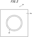
- FIG. 2 is a diagram of the laminate 100 as viewed from above.
- the half cut section 130 has a circular shape in a top view as illustrated in FIG. 2 . It should be noted, however, that the shape of the half cut section 130 in a top view is not limited to a circular shape.
- the half cut section 130 may have a polygonal shape such as a quadrangular shape in a top view.
- the laminate of the present embodiment satisfies P1 > P2 when peeling force at an interface of the first retention film 120a and the thin film structural body 110 in a 90° peeling test in accordance with JIS Z0237:2009 is taken to be P1 (N/25 mm) and peeling force at an interface of the second retention film 120b and the thin film structural body 110 in a 90° peeling test in accordance with JIS Z0237:2009 is taken to be P2 (N/25 mm).
- the laminate 100 of the present embodiment including the half cut section 130 in the thickness direction as previously described, a single-side peeled laminate formed of the thin film structural body 110 and the first retention film 120a can easily be peeled from the second retention film 120b, inside of the half cut section 130, when the thin film structural body 110 is to be bonded to an object serving as an adherend.
- the thin film structural body 110 can closely adhere to the two retention films without a pressure-sensitive adhesive layer, an adhesive, or the like interposed therebetween.
- the laminate 100 of the present embodiment has high environment testing durability and can inhibit the occurrence of waviness.
- the laminate 100 of the present embodiment makes it possible to smoothly peel the retention film having low peeling force (second retention film 120b) from the thin film structural body 110 while maintaining a stacked state of the retention film having high peeling force (first retention film 120a) and the thin film structural body 110. Furthermore, damage to a fine irregularity structure is inhibited during peeling of a retention film, and particularly during peeling of the second retention film 120b.
- peeling of the first retention film 120a can be performed smoothly by, after peeling off the second retention film 120b, bonding the thin film structural body 110 to a base plate or the like in advance.
- the peeling force P1 at the interface of the first retention film 120a and the thin film structural body 110 and the peeling force P2 at the interface of the second retention film 120b and the thin film structural body 110 are each more than 0 N/25 mm, preferably 0.05 N/25 mm or more, and preferably 0.5 N/25 mm or less.
- P1 and P2 are 0.05 N/25 mm or more, spontaneous peeling of the retention films due to external factors or the like can be inhibited.
- P1 and P2 are 0.5 N/25 mm or less, damage to a fine irregularity structure of the thin film structural body 110 can be more sufficiently inhibited during peeling of a retention film.
- the difference (P1 - P2) between the peeling force P1 at the interface of the first retention film 120a and the thin film structural body 110 and the peeling force P2 at the interface of the second retention film 120b and the thin film structural body is not specifically limited but is preferably 0.03 N/25 mm or more, and is preferably 0.3 N/25 mm or less.
- P1 - P2 is 0.03 N/25 mm or more, a retention film, and particularly the second retention film 120b, can be smoothly peeled from the thin film structural body 110 while also more effectively inhibiting damage to the thin film structural body 110 and a fine irregularity structure at the surface thereof.
- P1 - P2 is 0.3 N/25 mm or less, it is possible to more effectively inhibit damage to the thin film structural body 110 and a fine irregularity structure at the surface thereof when the first retention film 120a is peeled from the thin film structural body.
- adjustment of the peeling force at an interface of a retention film and the thin film structural body 110 can be performed as appropriate through operations such as altering a constituent material of the thin film structural body 110, altering a fine irregularity structure of the thin film structural body 110, altering the thickness of a part of the thin film structural body 110 that is not a fine irregularity structure (described further below), adding an additive such as a fluorine-containing additive to a constituent material of a base substrate of the retention film (described further below), altering the thickness of the retention film, providing the retention film with an inorganic film, providing the retention film with a release film, and altering a constituent material or the thickness of the inorganic film or the release film.
- adjustment of P1 - P2 can be performed as appropriate through any combination of the operations described above.
- the thin film structural body 110 used in the present embodiment has the first fine irregularity structure 110-1 and the second fine irregularity structure 110-2 at the faces thereof.
- fine irregularity patterns protrusions that protrude in the thickness direction of the laminate and depressions that are depressed in the thickness direction of the laminate
- the protrusions and depressions may be arranged periodically (for example, a staggered or rectangular grid), or may be arranged randomly.
- the shape of the protrusions and the depressions is not specifically limited and may be a bullet shape, a pyramidal shape, a columnar shape, a needle shape, or the like. Note that the shape of a depression is the shape formed by an inner wall of the depression.
- the thin film structural body 110 can be produced using a UV (ultraviolet) curable resin, for example.
- the UV-curable resin may be a UV-curable acrylic-based resin, a UV-curable epoxy-based resin, or the like, for example, without any specific limitations.
- the average period (pitch) of irregularity patterns constituting the first fine irregularity structure 110-1 and the second fine irregularity structure 110-2 is preferably equal to or less than a wavelength of visible light (for example, 830 nm or less), more preferably 350 nm or less, and even more preferably 280 nm or less, and is more preferably 100 nm or more, and even more preferably 150 nm or more.
- the depth of depressions (height of protrusions) of the irregularity patterns constituting the first fine irregularity structure 110-1 and the second fine irregularity structure 110-2 is not specifically limited but is preferably 150 nm or more, and more preferably 190 nm or more, and is preferably 300 nm or less, and more preferably 230 nm or less.
- the arrangement of depressions and protrusions, the average period of the irregularity pattern, the depth of depressions, and so forth may be the same or different for the first fine irregularity structure 110-1 and the second fine irregularity structure 110-2 of the thin film structural body 110.
- the thickness of the thin film structural body 110 used in the present embodiment is preferably 10 ⁇ m or less, more preferably 5 ⁇ m or less, and even more preferably 1 ⁇ m or less, and is preferably 0.1 ⁇ m or more.
- Such a thin film structural body 110 can suitably be used in an application where both improvement of anti-reflection performance and reduction of thickness are required, such as in a notebook PC, tablet PC, smartphone, mobile phone, or the like that is equipped with an image sensor.
- the thickness of the thin film structural body 110 is the distance in the stacking direction or film thickness direction between the apex of a highest protrusion formed at one face and an apex of a highest protrusion formed at the other face as indicated by T 1 in FIG. 1 .
- the thickness of a part that is not a fine irregularity structure in the thin film structural body 110 used in the present embodiment is preferably 200 nm or less.
- the thin film structural body 110 can be more reliably peeled from a single-side peeled laminate after being bonded onto a base plate through an adhesive, and an optical body can be formed with high precision.
- the thickness of the part of the thin film structural body 110 that is not a fine irregularity structure can be set as 0.01 ⁇ m or more from a viewpoint of feasibility.
- the thickness of the part of the thin film structural body 110 that is not a fine irregularity structure is the distance in the stacking direction or film thickness direction between an apex of a deepest depression formed at one face and an apex of a deepest depression formed at the other face as indicated by T 2 in FIG. 1 .
- the thin film structural body 110 can be produced by, for example, preparing a base substrate and two fine irregularity layers as separate members and then forming the fine irregularity layers at both faces of the base substrate. However, it is preferable that the thin film structural body 110 is formed of a single member from a viewpoint of avoiding deterioration of optical properties.
- a laminate 100 that includes a thin film structural body 110 formed of a single member in this manner can be produced by the subsequently described method of producing a laminate 100, for example.
- the two retention films sandwich the thin film structural body 110. These two retention films are provided for protection of the thin film structural body 110, improvement of handleability, and so forth.
- the first retention film 120a has a third fine irregularity structure 120a-1 at a face that is in contact with the thin film structural body 110 and the second retention film 120b has a fourth fine irregularity structure 120b-1 at a face that is in contact with the thin film structural body 110.
- a fine irregularity pattern protrusions that protrude in the thickness direction of the laminate 100 and depressions that are depressed in the thickness direction of the laminate 100
- the third fine irregularity structure 120a-1 of the first retention film 120a is preferably an inverted structure of the first fine irregularity structure 110-1 of the thin film structural body 110
- the fourth fine irregularity structure 120b-1 of the second retention film 120b is preferably an inverted structure of the second fine irregularity structure 110-2 of the thin film structural body 110.
- the fine irregularity structure of the first retention film 120a and the fine irregularity structure of the second retention film 120b interlock, without gaps, with the fine irregularity structures of the thin film structural body 110.
- the thin film structural body 110 can closely adhere to the retention films 120a and 120b through frictional force due to mechanical joining through the fine irregularity structures of both the thin film structural body 110 and the retention films 120a and 120b.
- This effect of close adherence through frictional force due to interlocking of fine irregularity structures without gaps is referred to as an "anchor effect".
- anchor effect Through this anchor effect, it is possible to maintain a closely adhered state of the thin film structural body 110 with the retention films 120a and 120b even without a pressure-sensitive adhesive, an adhesive, or the like interposed therebetween.
- the average period (pitch) of the irregularity patterns constituting the third fine irregularity structure 120a-1 and the fourth fine irregularity structure 120b-1 is preferably equal to or less than a wavelength of visible light (for example, 830 nm or less), more preferably 350 nm or less, and even more preferably 280 nm or less, and is more preferably 100 nm or more, and even more preferably 150 nm or more in the same way as for the first fine irregularity structure 110-1 and the second fine irregularity structure 110-2.
- the retention films 120a and 120b can each be produced from a base substrate, for example. Moreover, the retention films 120a and 120b that each have a fine irregularity structure at a surface thereof can be produced as illustrated in FIG. 3 , for example, by forming a fine irregularity layer 122 on a base substrate 121.
- the material is preferably a material that is transparent and does not easily rupture, and may be PET (polyethylene terephthalate), TAC (triacetyl cellulose), or the like.
- Formation of the fine irregularity layer 122 on the base substrate 121 can be achieved by, for example, implementing a method including a step of applying an uncured UV-curable resin onto one face of the base substrate 121, a step of bringing a roll on which a corresponding irregularity pattern has been formed into close contact with the applied UV-curable resin and transferring an irregularity pattern to the UV-curable resin, a step of irradiating the applied UV-curable resin with UV light to cure the UV-curable resin, and a step of peeling the UV-curable resin that has been cured from the roll.
- the UV-curable resin may be a UV-curable acrylic-based resin, a UV-curable epoxy-based resin, or the like, for example, without any specific limitations.
- various additives such as curing initiators may be added to the UV-curable resin as necessary.
- the method by which the laminate 100 of the present embodiment is produced is not specifically limited and can be selected as appropriate depending on the objective.
- the following describes a specific example of a method for producing the laminate 100 with reference to FIGS. 4A to 4C .
- the one example of a method includes a step of sandwiching a UV-curable resin between two retention films each having a fine irregularity structure at a surface thereof and performing pressure bonding thereof (sandwiching and pressure bonding step), a step of irradiating the UV-curable resin that has been sandwiched with UV light to cure the UV-curable resin (curing step), and a step of forming a half cut section 130 (half cut section forming step).
- first retention film 120a having third fine irregularity structure 120a-1 at surface and second retention film 120b having fourth fine irregularity structure 120b-1 at surface
- the first retention film 120a and the second retention film 120b are as previously described.
- a UV-curable resin 151 is sandwiched between the above-described first retention film 120a and second retention film 120b such that the fine irregularity structures of the first retention film 120a and the second retention film 120b face each other as illustrated in FIG. 4A .
- the UV-curable resin may be a UV-curable acrylic-based resin, a UV-curable epoxy-based resin, or the like, for example, without any specific limitations.
- UV-curable resin 151 various additives such as curing initiators may be added to the UV-curable resin 151 as necessary.
- a monomer such as an ethylene oxide-based (EO-based) acrylic monomer, a propylene oxide-based (PO-based) acrylic monomer, or a fluorene-based monomer may be added to the UV-curable resin 151 from a viewpoint of increasing peelability and shape retainability.
- the viscosity of the UV-curable resin 151 is preferably 30 cps or less.
- the viscosity of the UV-curable resin 151 is 30 cps or less, it is possible to reduce the thickness of a part that is not a fine irregularity structure to 200 nm or less more easily in formation of the thin film structural body 110.
- the sandwiched body is pressure bonded in a sandwiching direction through a pressure bonding device such as a roll laminator 160.
- a pressure bonding device such as a roll laminator 160.
- the thickness of the obtained thin film structural body 110 (T 1 in FIG. 1 ) and the thickness of the part of the thin film structural body 110 that is not a fine irregularity structure (T 2 in FIG. 1 ) can also be adjusted by adjusting the feed rate by the roll laminator.
- the second retention film 120b is positioned at a lower side and the first retention film 120a is positioned at an upper side relative to the roll laminator 160 in FIG. 4A , the positional relationship thereof is not specifically limited.
- the UV-curable resin 151 that has been sandwiched is irradiated with UV light to cure the UV-curable resin 151 as illustrated in FIG. 4B .
- a thin film structural body 110 having fine irregularity structures at both faces such as illustrated in FIG. 1 , is formed as a single member, and a laminate 100 is obtained.
- the curing step may be performed at the same timing as the sandwiching and pressure bonding step.
- first fine irregularity structure 110-1 that is interlocked, without gaps, with the third fine irregularity structure 120a-1 of the first retention film 120a is formed at one face of the thin film structural body 110
- second fine irregularity structure 110-2 that is interlocked, without gaps, with the fourth fine irregularity structure 120b-1 of the second retention film 120b is formed at the other face of the thin film structural body 110.
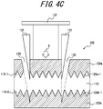
- a half cut section 130 is formed by, in a state in which the laminate 100 is pressed in a direction of arrow A by an air cylinder 132, punching the periphery of the pressed part using a blade 131 as illustrated in FIG. 4C .
- the air cylinder 132 keeps the laminate 100 in a pressed state until the blade 131 has been withdrawn from the laminate 100.
- uprising of approximately 10% of film thickness at a severed part arises when a half cut section is formed by laser cutting, but by making the blade 131 a single-edged blade in the half cut section forming step according to the present disclosure, uprising of a severed part inside of the half cut section 130 can be reduced.
- a presently disclosed method of forming an optical body on a base plate includes peeling the first retention film 120a and the second retention film 120b from the presently disclosed laminate 100 set forth above and stacking the thin film structural body 110 on a base plate via an adhesive.
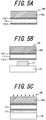
- the following describes a method of forming an optical body on a base plate according to one embodiment of the present disclosure (hereinafter, also referred to as the "formation method of the present embodiment") with reference to FIGS. 5A to 5E .
- FIGS. 5A to 5E are overviews illustrating the formation method of the present embodiment.
- the formation method of the present embodiment includes a first peeling step, an application step, a pressing step, a curing step, and a second peeling step.
- a single-side peeled laminate formed of the thin film structural body 110 and the first retention film 120a is peeled from the second retention film 120b illustrated in FIG. 1 , inside of the half cut section 130, and is placed in a state (single-side peeled laminate 100') illustrated in FIG. 5A .
- the single-side peeled laminate can be smoothly peeled from the second retention film 120b while also maintaining a stacked state of the first retention film 120a and the thin film structural body 110, and inhibiting damage to the second fine irregularity structure 110-2.
- an adhesive 171 is applied onto a base plate 170 in the application step as illustrated in FIG. 5B .
- the adhesive 171 is not specifically limited and may, for example, be a composition containing a UV-curable resin such as a UV-curable acrylic-based resin or a UV-curable epoxy-based resin.
- the material forming the base plate 170 is not specifically limited and can be selected as appropriate depending on the objective of forming the optical body.
- the material may be glass, glass that is surface coated with any organic material (for example, an epoxy acrylate copolymer), polymethyl methacrylate (PMMA), a cycloolefin copolymer (COC), a cycloolefin polymer (COP), or the like.
- the single-side peeled laminate 100' is pressed against the adhesive 171 that has been applied onto the base plate 170 such that the face where the second retention film 120b has been peeled off faces toward the base plate 170 in the pressing step as illustrated in FIG. 5C .
- the pressed adhesive 171 spreads out between the base plate 170 and the thin film structural body 110.
- the pressed adhesive 171 is irradiated with UV light to cure the adhesive 171 while in a state in which pressing is maintained.
- the cured adhesive 171 strongly adheres to the base plate 170 and the thin film structural body 110.
- a thin film structural body 110 (or optical body 200) can be formed in a partial manner and with high precision even with respect to a base plate to which adhesion is difficult (for example, a base plate formed of a polymer such as a cycloolefin copolymer (COC), a cycloolefin polymer (COP), or an epoxy acrylate copolymer).
- a base plate formed of a polymer such as a cycloolefin copolymer (COC), a cycloolefin polymer (COP), or an epoxy acrylate copolymer.
- the cured adhesive 171' can also enter depressions in a face at the base plate 170 side of the thin film structural body 110 as illustrated in FIG. 5E .
- the cured adhesive 171' can have a fine irregularity structure at a surface at the thin film structural body 110 side thereof.
- Such an optical body 200 has excellent anti-reflection performance and can, for example, have an average reflectance of 1% or less in a wavelength range of 400 nm to 750 nm.
- a presently disclosed camera module-equipped device includes a camera module and a display panel, wherein the display panel includes an adhesive layer stacked on at least part of a surface thereof and a thin film structural body stacked on the adhesive layer.
- the thin film structural body has fine irregularity structures at both faces thereof.
- the camera module is arranged such that the camera module and the thin film structural body face each other.
- an image sensor of the camera module can capture a still image or a video via the thin film structural body having fine irregularity structures at both faces, and thus reflection of light can be suppressed, and color irregularities, ghosts, and the like in a captured image that is acquired can be inhibited.
- the camera module-equipped device may, more specifically, be a notebook PC, a tablet PC, a smartphone, a mobile phone, or the like.
- the following describes a camera module-equipped device according to one embodiment of the present disclosure (hereinafter, also referred to as the "device according to the present embodiment") with reference to FIG. 6 .
- FIG. 6 is a schematic overview illustrating a region in proximity to a camera module of the camera module-equipped device of the present embodiment.
- the camera module-equipped device 300 of the present embodiment includes a camera module 310 and a display panel 311.
- a light shielding region 312 and a transparent region (non-light shielding region) 313 are formed at one surface of the display panel 311.
- an adhesive layer 314 is stacked and, in addition thereto, a thin film structural body 315 is stacked on the adhesive layer 314.
- the display panel 311 is preferably transparent in order that it can be used as a liquid-crystal display, a touch panel, or the like.
- the display panel 311 may be formed of glass, glass that is surface coated with any organic material, polymethyl methacrylate (PMMA), or the like.
- PMMA polymethyl methacrylate
- the thin film structural body 315 is as previously described for the thin film structural body 110 included in the presently disclosed laminate 100 set forth above.
- the adhesive layer 314 and the thin film structural body 315 can be formed on the display panel 311, serving as a base plate, by the presently disclosed method of forming an optical body on a base plate set forth above, and using the presently disclosed laminate 100 set forth above. In such a situation, the adhesive layer 314 and the thin film structural body 315 respectively correspond to the cured adhesive 171' and the thin film structural body 110 described for the formation method of the present embodiment.
- the camera module 310 is arranged such that the camera module 310 and the thin film structural body 315 face each other as illustrated in FIG. 6 .
- testing of detachment upon punching and testing of detachment after vibration were performed by the following procedures for laminates produced in the examples and comparative examples.
- half cut processing was evaluated based on the results of testing of detachment upon punching and testing of detachment after vibration.
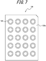
- Half cut sections 130 were formed at 20 locations in 5 rows by 4 columns in a laminate 100 as illustrated in FIG. 7 . When each of these half cut sections 130 was formed, it was confirmed whether or not a single-side peeled laminate inside of the half cut section 130 became detached.
- the outer dimensions of the laminate 100 were set as 50 mm in length by 40 mm in width. Moreover, the interval between centers of adjacent half cut sections 130 was set as 9 mm.
- the testing of detachment after vibration was performed by subjecting a laminate 100 packaged in corrugated cardboard or the like to vibration under the following conditions.
- Half cut processing was evaluated by the following standard based on the results of testing of detachment upon punching and testing of detachment after vibration.
- a laminate 100 for which detachment did not occur in testing of detachment upon punching but did occur in testing of detachment after vibration was given a B evaluation rather than a C evaluation because such a laminate 100 can be transported without detachment by transporting the laminate 100 under transportation conditions with little vibration.
- the following material was used as the base substrate of a retention film in a laminate for which testing of detachment upon punching and testing of detachment after vibration were performed. Note that the following material has four thicknesses (50 ⁇ m, 75 ⁇ m, 100 ⁇ m, and 125 ⁇ m), and thus a film of one or other of these thicknesses was used.
- Base substrate COSMOSHINE A4300 PET film produced by Toyobo Co., Ltd.
- resins 1 to 3 are resins that differ in terms of storage modulus at 25°C.
- Resin 1 has a storage modulus at 25°C of 4.2 GPa
- resin 2 has a storage modulus at 25°C of 1.1 GPa
- resin 3 has a storage modulus at 25°C of 510 MPa.
- the thickness of a base substrate 121 of a second retention film 120b, the storage modulus of a fine irregularity layer 122 of the second retention film 120b, and the storage modulus of a fine irregularity layer 122 of the first retention film 120a were set as follows as conditions that were common for each example.
- the thin film structural body 110 was peeled from the second retention film 120b to a degree that did not cause detachment, and the anchor effect between the thin film structural body 110 and the second retention film 120b was lost due to deformation of the first retention film 120a being large, and thus detachment did occur in testing of detachment after vibration.
- the thickness of a base substrate 121 of the second retention film 120b, the thickness of a base substrate 121 of a first retention film 120a, and the storage modulus of a fine irregularity layer 122 of the first retention film 120a were set as follows as conditions that were common for each example.
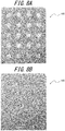
- FIG. 8A illustrates the appearance of a laminate 100 according to Comparative Example 2 after testing of detachment upon punching.
- detachment occurred for all of the half cut sections 130 at the 20 locations in 5 rows by 4 columns as illustrated in FIG. 8A.
- FIG. 8B illustrates the appearance of a laminate 100 according to Example 4 after testing of detachment upon punching.
- detachment did not occur for any of the half cut sections 130 at the 20 locations in 5 rows by 4 columns as illustrated in FIG. 8B .
- the thickness of the base substrate 121 of the first retention film 120a is preferably 100 ⁇ m or less.
- the storage modulus at 25°C of the fine irregularity layer 122 of the second retention film 120b is preferably 1.1 GPa or less.
- the present disclosure it is possible to provide a laminate that enables simple peeling of a thin film structural body having a fine irregularity structure at a surface thereof when the thin film structural body is to be bonded to an object serving as an adherend, that has improved environment testing durability, and in which waviness is inhibited. Moreover, according to the present disclosure, it is possible to provide a method of producing this laminate. Furthermore, according to the present disclosure, it is possible to provide a method of forming an optical body having excellent anti-reflection performance on a base plate using this laminate. Also, according to the present disclosure, it is possible to provide a camera module-equipped device that can acquire a captured image in which color irregularities, ghosts, and the like are inhibited.
Landscapes
- Physics & Mathematics (AREA)
- General Physics & Mathematics (AREA)
- Engineering & Computer Science (AREA)
- Optics & Photonics (AREA)
- Mechanical Engineering (AREA)
- Health & Medical Sciences (AREA)
- Manufacturing & Machinery (AREA)
- Ophthalmology & Optometry (AREA)
- Laminated Bodies (AREA)
- Surface Treatment Of Optical Elements (AREA)
- Blocking Light For Cameras (AREA)
Abstract
Description
- The present disclosure relates to a laminate, a method of producing a laminate, a method of forming an optical body, and a camera module-equipped device.
- In display devices such as liquid-crystal displays and optical devices such as cameras, an incident surface of light of a substrate such as a display panel or a lens is often subjected to anti-reflection treatment in order to avoid deterioration of visibility and image quality (occurrence of color irregularities, ghosts, etc.) caused by reflection of extraneous light. This anti-reflection treatment may be performed by a conventionally known method in which a fine irregularity structure is formed at the incident surface of light so as to reduce reflectance.
- Formation of a fine irregularity structure at the incident surface of light can be achieved by, for example, affixing a film having a fine irregularity structure at a surface thereof to the incident surface. This method is highly advantageous from viewpoints such as that processing of the substrate itself is not necessary, that the film itself can be distributed to market (i.e., is portable), and that a fine irregularity structure can be formed in a partial manner in a target region at the surface of the substrate.
- In a situation in which a film having anti-reflection function is itself to be distributed, performing half cut processing of a film in which peelable films are stacked makes it is easy to peel off a required part when the film having anti-reflection function is to be bonded to an object serving as an adherend.
- For example, Patent Literature (PTL) 1 discloses a pressure-sensitive adhesive film for half cut processing that includes a substrate layer and a pressure-sensitive adhesive layer. In another example, PTL 2 discloses half cutting a functional optical film that is stacked on a conductive metal layer. In the invention disclosed in PTL 2, the functional optical film is affixed to the conductive metal layer via an adhesive.
-
- PTL 1:
JP 2017-149948 A - PTL 2:
JP 2004-151633 A - The film disclosed in
PTL 1 is affixed through a pressure-sensitive adhesive layer, and the film disclosed in PTL 2 is affixed through an adhesive. A film that is affixed via a pressure-sensitive adhesive layer, an adhesive, or the like faces issues such as environment testing durability being low and waviness readily occurring. - The present disclosure is directed to solving the various problems in the conventional art set forth above and achieving the following objects. Specifically, one object of the present disclosure is to provide a laminate that enables simple peeling of a thin film structural body having a fine irregularity structure at a surface thereof when the thin film structural body is to be bonded to an object serving as an adherend, that has improved environment testing durability, and in which waviness is inhibited. Another object of the present disclosure is to provide a method of producing this laminate. Another object of the present disclosure is to provide a method of forming an optical body having excellent anti-reflection performance on a base plate using this laminate. Another object of the present disclosure is to provide a camera module-equipped device that can acquire a captured image in which color irregularities, ghosts, and the like are inhibited.
- The following are provided as a solution to the problems set forth above.
- <1> A laminate comprising a thin film structural body and retention films, wherein
- a first retention film is stacked on one face of the thin film structural body and a second retention film is stacked on another face of the thin film structural body,
- the thin film structural body has a first fine irregularity structure at a face that is in contact with the first retention film and has a second fine irregularity structure at a face that is in contact with the second retention film,
- the first retention film has a third fine irregularity structure at a face that is in contact with the thin film structural body,
- the second retention film has a fourth fine irregularity structure at a face that is in contact with the thin film structural body,
- the laminate includes a half cut section in a thickness direction, and
- the second retention film contains a UV-curable resin, and the UV-curable resin has a storage modulus at 25°C of 1.1 GPa or less.
- <2> The laminate according to <1>, wherein a base substrate of the first retention film has a thickness of 100 µm or less.
- <3> The laminate according to <1> or <2>, wherein P1 > P2 is satisfied when peeling force at an interface of the first retention film and the thin film structural body in a 90° peeling test in accordance with JIS Z0237:2009 is taken to be P1 (N/25 mm) and peeling force at an interface of the second retention film and the thin film structural body in a 90° peeling test in accordance with JIS Z0237:2009 is taken to be P2 (N/25 mm).
- <4> The laminate according to any one of <1> to <3>, wherein the half cut section has a circular shape or a polygonal shape in a top view of the laminate.
- <5> The laminate according to any one of <1> to <4>, wherein the thin film structural body has a thickness of 5 µm or less.
- <6> The laminate according to any one of <1> to <5>, wherein the first retention film contains a UV-curable resin.
- <7> The laminate according to any one of <1> to <6>, wherein the third fine irregularity structure is an inverted structure of the first fine irregularity structure and the fourth fine irregularity structure is an inverted structure of the second fine irregularity structure.
- <8> The laminate according to any one of <1> to <7>, wherein the first fine irregularity structure, the second fine irregularity structure, the third fine irregularity structure, and the fourth fine irregularity structure are each formed of an irregularity pattern having a pitch equal to or less than a wavelength of visible light.
- <9> A method of producing a laminate comprising a step of, in formation of the half cut section in the laminate according to any one of <1> to <8>, forming the half cut section with the laminate in a pressed state.
- <10> A method of forming an optical body on a base plate comprising peeling the first retention film and the second retention film from the laminate according to any one of <1> to <8> and stacking the thin film structural body on a base plate via an adhesive.
- <11> The method of forming an optical body on a base plate according to <10> comprising:
- a first peeling step of peeling a single-side peeled laminate formed of the thin film structural body and the first retention film from the second retention film, inside of the half cut section, to obtain the single-side peeled laminate;
- an application step of applying the adhesive onto the base plate;
- a pressing step of pressing the single-side peeled laminate against the adhesive that has been applied such that a face where the second retention film has been peeled off faces toward the base plate;
- a curing step of irradiating the adhesive that has been pressed with UV light to cure the adhesive; and
- a second peeling step of releasing pressing of the single-side peeled laminate and peeling the thin film structural body from the single-side peeled laminate to form an optical body formed of the adhesive that has been cured and the thin film structural body on the base plate.
- <12> A camera module-equipped device comprising a camera module and a display panel, wherein
- the display panel includes an adhesive layer stacked on at least part of a surface thereof and a thin film structural body stacked on the adhesive layer,
- the camera module is arranged such that the camera module and the thin film structural body face each other, and
- the thin film structural body is a thin film structural body obtained by peeling the first retention film and the second retention film from the laminate according to any one of <1> to <8>.
- According to the present disclosure, it is possible to provide a laminate that enables simple peeling of a thin film structural body having a fine irregularity structure at a surface thereof when the thin film structural body is to be bonded to an object serving as an adherend, that has improved environment testing durability, and in which waviness is inhibited. Moreover, according to the present disclosure, it is possible to provide a method of producing this laminate. Furthermore, according to the present disclosure, it is possible to provide a method of forming an optical body having excellent anti-reflection performance on a base plate using this laminate. Also, according to the present disclosure, it is possible to provide a camera module-equipped device that can acquire a captured image in which color irregularities, ghosts, and the like are inhibited.
- In the accompanying drawings:
-
FIG. 1 is a schematic cross-sectional view illustrating a laminate according to one embodiment of the present disclosure; -
FIG. 2 is a top view illustrating a laminate according to one embodiment of the present disclosure; -
FIG. 3 is a schematic cross-sectional view illustrating a retention film of a laminate according to one embodiment of the present disclosure; -
FIG. 4A is an overview illustrating one step in one example of a method for producing a laminate according to one embodiment of the present disclosure; -
FIG. 4B is an overview illustrating one step in one example of a method for producing a laminate according to one embodiment of the present disclosure; -
FIG. 4C is an overview illustrating one step in one example of a method for producing a laminate according to one embodiment of the present disclosure; -
FIG. 5A is an overview illustrating one step in a method of forming an optical body on a base plate according to one embodiment of the present disclosure; -
FIG. 5B is an overview illustrating one step in a method of forming an optical body on a base plate according to one embodiment of the present disclosure; -
FIG. 5C is an overview illustrating one step in a method of forming an optical body on a base plate according to one embodiment of the present disclosure; -
FIG. 5D is an overview illustrating one step in a method of forming an optical body on a base plate according to one embodiment of the present disclosure; -
FIG. 5E is an overview illustrating one step in a method of forming an optical body on a base plate according to one embodiment of the present disclosure; -
FIG. 6 is a schematic overview illustrating a region in proximity to a camera module of a camera module-equipped device according to one embodiment of the present disclosure; -
FIG. 7 is a top view illustrating one example of a laminate according to one embodiment of the present disclosure when a punching test is performed using the laminate; -
FIG. 8A illustrates the appearance of a laminate according to Comparative Example 2 after testing of detachment upon punching; and -
FIG. 8B illustrates the appearance of a laminate according to Example 4 after testing of detachment upon punching. - The following provides a detailed description of the present disclosure based on embodiments.
- A presently disclosed laminate includes a thin film structural body and retention films. The thin film structural body has a first retention film stacked on one face of the thin film structural body and has a second retention film stacked on another face of the thin film structural body. The thin film structural body has a first fine irregularity structure at a face that is in contact with the first retention film and has a second fine irregularity structure at a face that is in contact with the second retention film. The first retention film has a third fine irregularity structure at a face that is in contact with the thin film structural body and the second retention film has a fourth fine irregularity structure at a face that is in contact with the thin film structural body. The laminate includes a half cut section in a thickness direction. The second retention film contains a UV-curable resin, and this UV-curable resin has a storage modulus at 25°C of 1.1 GPa or less.
- The presently disclosed laminate serves as an intermediate product used in formation of an optical body on a base plate (described further below).
- The following describes a laminate according to one embodiment of the present disclosure (hereinafter, also referred to as the "laminate of the present embodiment") with reference to
FIG. 1 , etc. - As illustrated in
FIG. 1 , thelaminate 100 of the present embodiment includes a thin filmstructural body 110 and two retention films (i.e., afirst retention film 120a and asecond retention film 120b). Thefirst retention film 120a is stacked on one face of the thin filmstructural body 110 and thesecond retention film 120b is stacked on another face of the thin filmstructural body 110. In other words, the thin filmstructural body 110 is sandwiched between the two retention films. The thin filmstructural body 110 has a first fine irregularity structure 110-1 at a surface where thefirst retention film 120a is stacked and has a second fine irregularity structure 110-2 at a surface where thesecond retention film 120b is stacked. Moreover, thefirst retention film 120a has a thirdfine irregularity structure 120a-1 and thesecond retention film 120b has a fourthfine irregularity structure 120b-1. - The
laminate 100 of the present embodiment also includes ahalf cut section 130 in a thickness direction. The "thickness direction" is the direction of stacking of thefirst retention film 120a, the thin filmstructural body 110, and thesecond retention film 120b. Thehalf cut section 130 is a cut line that is formed in order to make it easier for a single-side peeled laminate formed of the thin filmstructural body 110 and thefirst retention film 120a to be peeled from thesecond retention film 120b. Thehalf cut section 130 completely severs thefirst retention film 120a and the thin filmstructural body 110 and severs up to partway through thesecond retention film 120b as illustrated inFIG. 1 . -
FIG. 2 is a diagram of the laminate 100 as viewed from above. Thehalf cut section 130 has a circular shape in a top view as illustrated inFIG. 2 . It should be noted, however, that the shape of thehalf cut section 130 in a top view is not limited to a circular shape. For example, thehalf cut section 130 may have a polygonal shape such as a quadrangular shape in a top view. - The laminate of the present embodiment satisfies P1 > P2 when peeling force at an interface of the
first retention film 120a and the thin filmstructural body 110 in a 90° peeling test in accordance with JIS Z0237:2009 is taken to be P1 (N/25 mm) and peeling force at an interface of thesecond retention film 120b and the thin filmstructural body 110 in a 90° peeling test in accordance with JIS Z0237:2009 is taken to be P2 (N/25 mm). - As a result of the
laminate 100 of the present embodiment including thehalf cut section 130 in the thickness direction as previously described, a single-side peeled laminate formed of the thin filmstructural body 110 and thefirst retention film 120a can easily be peeled from thesecond retention film 120b, inside of thehalf cut section 130, when the thin filmstructural body 110 is to be bonded to an object serving as an adherend. - Moreover, as a result of the thin film
structural body 110 being sandwiched by the two retention films with faces having fine irregularity structures (thirdfine irregularity structure 120a-1 and fourthfine irregularity structure 120b-1) in contact therewith in thelaminate 100 of the present embodiment as previously described, the thin filmstructural body 110 can closely adhere to the two retention films without a pressure-sensitive adhesive layer, an adhesive, or the like interposed therebetween. Through the thin filmstructural body 110 and the two retention films being closely adhered without a pressure-sensitive adhesive layer, an adhesive, or the like interposed therebetween in this manner in thelaminate 100 of the present embodiment, thelaminate 100 of the present embodiment has high environment testing durability and can inhibit the occurrence of waviness. - Moreover, as a result of there being a difference between one face and the other face of the thin film
structural body 110 in terms of peeling force with the retention film stacked thereat as previously described, thelaminate 100 of the present embodiment makes it possible to smoothly peel the retention film having low peeling force (second retention film 120b) from the thin filmstructural body 110 while maintaining a stacked state of the retention film having high peeling force (first retention film 120a) and the thin filmstructural body 110. Furthermore, damage to a fine irregularity structure is inhibited during peeling of a retention film, and particularly during peeling of thesecond retention film 120b. In contrast, when peeling of either of the two retention films is attempted in a case in which peeling force with a retention film is the same at both one face and the other face of the thin filmstructural body 110, splitting of the thin filmstructural body 110 may occur near the center thereof, the majority of a fine irregularity structure may be taken away to the retention film side, and it may not be possible to maintain sufficient quality until the thin filmstructural body 110 is actually used by a customer. - Note that peeling of the
first retention film 120a can be performed smoothly by, after peeling off thesecond retention film 120b, bonding the thin filmstructural body 110 to a base plate or the like in advance. - In the
laminate 100 of the present embodiment, the peeling force P1 at the interface of thefirst retention film 120a and the thin filmstructural body 110 and the peeling force P2 at the interface of thesecond retention film 120b and the thin filmstructural body 110 are each more than 0 N/25 mm, preferably 0.05 N/25 mm or more, and preferably 0.5 N/25 mm or less. When P1 and P2 are 0.05 N/25 mm or more, spontaneous peeling of the retention films due to external factors or the like can be inhibited. Moreover, when P1 and P2 are 0.5 N/25 mm or less, damage to a fine irregularity structure of the thin filmstructural body 110 can be more sufficiently inhibited during peeling of a retention film. - Note that in a case in which almost the entire surface of the thin film
structural body 110 is taken away to the retention film side during measurement of the peeling force at an interface of a retention film and the thin filmstructural body 110, it is judged that peeling of the measurement subject was not possible and that "peel strength measurement value: more than 0 N/25 mm" is not even satisfied. - In the
laminate 100 of the present embodiment, the difference (P1 - P2) between the peeling force P1 at the interface of thefirst retention film 120a and the thin filmstructural body 110 and the peeling force P2 at the interface of thesecond retention film 120b and the thin film structural body is not specifically limited but is preferably 0.03 N/25 mm or more, and is preferably 0.3 N/25 mm or less. When P1 - P2 is 0.03 N/25 mm or more, a retention film, and particularly thesecond retention film 120b, can be smoothly peeled from the thin filmstructural body 110 while also more effectively inhibiting damage to the thin filmstructural body 110 and a fine irregularity structure at the surface thereof. Moreover, when P1 - P2 is 0.3 N/25 mm or less, it is possible to more effectively inhibit damage to the thin filmstructural body 110 and a fine irregularity structure at the surface thereof when thefirst retention film 120a is peeled from the thin film structural body. - Note that adjustment of the peeling force at an interface of a retention film and the thin film
structural body 110 can be performed as appropriate through operations such as altering a constituent material of the thin filmstructural body 110, altering a fine irregularity structure of the thin filmstructural body 110, altering the thickness of a part of the thin filmstructural body 110 that is not a fine irregularity structure (described further below), adding an additive such as a fluorine-containing additive to a constituent material of a base substrate of the retention film (described further below), altering the thickness of the retention film, providing the retention film with an inorganic film, providing the retention film with a release film, and altering a constituent material or the thickness of the inorganic film or the release film. Accordingly, adjustment of P1 - P2 can be performed as appropriate through any combination of the operations described above. - The thin film
structural body 110 used in the present embodiment has the first fine irregularity structure 110-1 and the second fine irregularity structure 110-2 at the faces thereof. In other words, fine irregularity patterns (protrusions that protrude in the thickness direction of the laminate and depressions that are depressed in the thickness direction of the laminate) are formed at both faces of the thin filmstructural body 110. The protrusions and depressions may be arranged periodically (for example, a staggered or rectangular grid), or may be arranged randomly. Moreover, the shape of the protrusions and the depressions is not specifically limited and may be a bullet shape, a pyramidal shape, a columnar shape, a needle shape, or the like. Note that the shape of a depression is the shape formed by an inner wall of the depression. - The thin film
structural body 110 can be produced using a UV (ultraviolet) curable resin, for example. The UV-curable resin may be a UV-curable acrylic-based resin, a UV-curable epoxy-based resin, or the like, for example, without any specific limitations. - The average period (pitch) of irregularity patterns constituting the first fine irregularity structure 110-1 and the second fine irregularity structure 110-2 is preferably equal to or less than a wavelength of visible light (for example, 830 nm or less), more preferably 350 nm or less, and even more preferably 280 nm or less, and is more preferably 100 nm or more, and even more preferably 150 nm or more. By setting the pitch of an irregularity pattern at a surface of the thin film
structural body 110 as equal to or less than a wavelength of visible light (i.e., by providing a structure referred to as a "moth-eye structure" at the surface of the thin film structural body 110), further improvement of anti-reflection performance can be achieved. - The depth of depressions (height of protrusions) of the irregularity patterns constituting the first fine irregularity structure 110-1 and the second fine irregularity structure 110-2 is not specifically limited but is preferably 150 nm or more, and more preferably 190 nm or more, and is preferably 300 nm or less, and more preferably 230 nm or less.
- Note that the arrangement of depressions and protrusions, the average period of the irregularity pattern, the depth of depressions, and so forth may be the same or different for the first fine irregularity structure 110-1 and the second fine irregularity structure 110-2 of the thin film
structural body 110. - The thickness of the thin film
structural body 110 used in the present embodiment is preferably 10 µm or less, more preferably 5 µm or less, and even more preferably 1 µm or less, and is preferably 0.1 µm or more. Such a thin filmstructural body 110 can suitably be used in an application where both improvement of anti-reflection performance and reduction of thickness are required, such as in a notebook PC, tablet PC, smartphone, mobile phone, or the like that is equipped with an image sensor. - Note that the thickness of the thin film
structural body 110 is the distance in the stacking direction or film thickness direction between the apex of a highest protrusion formed at one face and an apex of a highest protrusion formed at the other face as indicated by T1 inFIG. 1 . - The thickness of a part that is not a fine irregularity structure in the thin film
structural body 110 used in the present embodiment is preferably 200 nm or less. When a laminate 100 including such a thin filmstructural body 110 is used in formation of an optical body by a subsequently described method of forming an optical body on a base plate according to one embodiment of the present disclosure, for example, the thin filmstructural body 110 can be more reliably peeled from a single-side peeled laminate after being bonded onto a base plate through an adhesive, and an optical body can be formed with high precision. On the other hand, the thickness of the part of the thin filmstructural body 110 that is not a fine irregularity structure can be set as 0.01 µm or more from a viewpoint of feasibility. - Note that the thickness of the part of the thin film
structural body 110 that is not a fine irregularity structure is the distance in the stacking direction or film thickness direction between an apex of a deepest depression formed at one face and an apex of a deepest depression formed at the other face as indicated by T2 inFIG. 1 . - The thin film
structural body 110 can be produced by, for example, preparing a base substrate and two fine irregularity layers as separate members and then forming the fine irregularity layers at both faces of the base substrate. However, it is preferable that the thin filmstructural body 110 is formed of a single member from a viewpoint of avoiding deterioration of optical properties. A laminate 100 that includes a thin filmstructural body 110 formed of a single member in this manner can be produced by the subsequently described method of producing a laminate 100, for example. - In the
laminate 100 of the present embodiment, the two retention films (i.e., thefirst retention film 120a and thesecond retention film 120b) sandwich the thin filmstructural body 110. These two retention films are provided for protection of the thin filmstructural body 110, improvement of handleability, and so forth. - As illustrated in
FIG. 1 , thefirst retention film 120a has a thirdfine irregularity structure 120a-1 at a face that is in contact with the thin filmstructural body 110 and thesecond retention film 120b has a fourthfine irregularity structure 120b-1 at a face that is in contact with the thin filmstructural body 110. In other words, a fine irregularity pattern (protrusions that protrude in the thickness direction of the laminate 100 and depressions that are depressed in the thickness direction of the laminate 100) is formed at a specific face of thefirst retention film 120a and a specific face of thesecond retention film 120b. This makes it simple to form fine irregularity structures at both faces of the thin filmstructural body 110. - Moreover, as illustrated in
FIG. 1 , the thirdfine irregularity structure 120a-1 of thefirst retention film 120a is preferably an inverted structure of the first fine irregularity structure 110-1 of the thin filmstructural body 110, and the fourthfine irregularity structure 120b-1 of thesecond retention film 120b is preferably an inverted structure of the second fine irregularity structure 110-2 of the thin filmstructural body 110. This makes it possible for the thin filmstructural body 110 and theretention films structural body 110, while also more effectively inhibiting damage to the thin filmstructural body 110 during peeling of a retention film. From the same viewpoints, it is more preferable that the fine irregularity structure of thefirst retention film 120a and the fine irregularity structure of thesecond retention film 120b interlock, without gaps, with the fine irregularity structures of the thin filmstructural body 110. Moreover, the thin filmstructural body 110 can closely adhere to theretention films structural body 110 and theretention films structural body 110 with theretention films - The average period (pitch) of the irregularity patterns constituting the third
fine irregularity structure 120a-1 and the fourthfine irregularity structure 120b-1 is preferably equal to or less than a wavelength of visible light (for example, 830 nm or less), more preferably 350 nm or less, and even more preferably 280 nm or less, and is more preferably 100 nm or more, and even more preferably 150 nm or more in the same way as for the first fine irregularity structure 110-1 and the second fine irregularity structure 110-2. - The
retention films retention films FIG. 3 , for example, by forming afine irregularity layer 122 on abase substrate 121. - Although no specific limitations are placed on the material forming the
base substrate 121, the material is preferably a material that is transparent and does not easily rupture, and may be PET (polyethylene terephthalate), TAC (triacetyl cellulose), or the like. - Formation of the
fine irregularity layer 122 on thebase substrate 121 can be achieved by, for example, implementing a method including a step of applying an uncured UV-curable resin onto one face of thebase substrate 121, a step of bringing a roll on which a corresponding irregularity pattern has been formed into close contact with the applied UV-curable resin and transferring an irregularity pattern to the UV-curable resin, a step of irradiating the applied UV-curable resin with UV light to cure the UV-curable resin, and a step of peeling the UV-curable resin that has been cured from the roll. Note that the UV-curable resin may be a UV-curable acrylic-based resin, a UV-curable epoxy-based resin, or the like, for example, without any specific limitations. Moreover, various additives such as curing initiators may be added to the UV-curable resin as necessary. - The method by which the
laminate 100 of the present embodiment is produced is not specifically limited and can be selected as appropriate depending on the objective. The following describes a specific example of a method for producing the laminate 100 with reference toFIGS. 4A to 4C . - The one example of a method includes a step of sandwiching a UV-curable resin between two retention films each having a fine irregularity structure at a surface thereof and performing pressure bonding thereof (sandwiching and pressure bonding step), a step of irradiating the UV-curable resin that has been sandwiched with UV light to cure the UV-curable resin (curing step), and a step of forming a half cut section 130 (half cut section forming step).
- First, two retention films each having a fine irregularity structure at a surface thereof (
first retention film 120a having thirdfine irregularity structure 120a-1 at surface andsecond retention film 120b having fourthfine irregularity structure 120b-1 at surface) are prepared. Thefirst retention film 120a and thesecond retention film 120b are as previously described. Next, a UV-curable resin 151 is sandwiched between the above-describedfirst retention film 120a andsecond retention film 120b such that the fine irregularity structures of thefirst retention film 120a and thesecond retention film 120b face each other as illustrated inFIG. 4A . Note that the UV-curable resin may be a UV-curable acrylic-based resin, a UV-curable epoxy-based resin, or the like, for example, without any specific limitations. Moreover, various additives such as curing initiators may be added to the UV-curable resin 151 as necessary. Furthermore, a monomer such as an ethylene oxide-based (EO-based) acrylic monomer, a propylene oxide-based (PO-based) acrylic monomer, or a fluorene-based monomer may be added to the UV-curable resin 151 from a viewpoint of increasing peelability and shape retainability. - The viscosity of the UV-
curable resin 151 is preferably 30 cps or less. When the viscosity of the UV-curable resin 151 is 30 cps or less, it is possible to reduce the thickness of a part that is not a fine irregularity structure to 200 nm or less more easily in formation of the thin filmstructural body 110. - As illustrated in
FIG. 4A , the sandwiched body is pressure bonded in a sandwiching direction through a pressure bonding device such as aroll laminator 160. By adjusting the pressure during pressure bonding in the sandwiching and pressure bonding step, it is possible to adjust the thickness of the obtained thin film structural body 110 (T1 inFIG. 1 ) and the thickness of the part of the thin filmstructural body 110 that is not a fine irregularity structure (T2 inFIG. 1 ). The thickness of the obtained thin film structural body 110 (T1 inFIG. 1 ) and the thickness of the part of the thin filmstructural body 110 that is not a fine irregularity structure (T2 inFIG. 1 ) can also be adjusted by adjusting the feed rate by the roll laminator. - It should be noted that although the
second retention film 120b is positioned at a lower side and thefirst retention film 120a is positioned at an upper side relative to theroll laminator 160 inFIG. 4A , the positional relationship thereof is not specifically limited. - In the curing step, the UV-
curable resin 151 that has been sandwiched is irradiated with UV light to cure the UV-curable resin 151 as illustrated inFIG. 4B . By curing the UV-curable resin 151, a thin filmstructural body 110 having fine irregularity structures at both faces, such as illustrated inFIG. 1 , is formed as a single member, and a laminate 100 is obtained. Note that the curing step may be performed at the same timing as the sandwiching and pressure bonding step. - In the thin film
structural body 110 that is obtained in this manner, a fine irregularity structure (first fine irregularity structure 110-1) that is interlocked, without gaps, with the thirdfine irregularity structure 120a-1 of thefirst retention film 120a is formed at one face of the thin filmstructural body 110, and a fine irregularity structure (second fine irregularity structure 110-2) that is interlocked, without gaps, with the fourthfine irregularity structure 120b-1 of thesecond retention film 120b is formed at the other face of the thin filmstructural body 110. - In the half cut section forming step, a
half cut section 130 is formed by, in a state in which thelaminate 100 is pressed in a direction of arrow A by anair cylinder 132, punching the periphery of the pressed part using ablade 131 as illustrated inFIG. 4C . Theair cylinder 132 keeps the laminate 100 in a pressed state until theblade 131 has been withdrawn from thelaminate 100. By pressing the laminate 100 using theair cylinder 132 in this manner, it is possible to prevent thefirst retention film 120a and the thin filmstructural body 110 being taken away by theblade 131 and the thin filmstructural body 110 being peeled from thesecond retention film 120b, inside of thehalf cut section 130, when theblade 131 is withdrawn. - When a half cut section is formed by laser cutting, for example, a lot of debris is formed, but since the
half cut section 130 is formed through punching using theblade 131 in the half cut section forming step according to the present disclosure, the formation of debris during formation of thehalf cut section 130 can be inhibited. - Moreover, uprising of approximately 10% of film thickness at a severed part arises when a half cut section is formed by laser cutting, but by making the blade 131 a single-edged blade in the half cut section forming step according to the present disclosure, uprising of a severed part inside of the
half cut section 130 can be reduced. - A presently disclosed method of forming an optical body on a base plate includes peeling the
first retention film 120a and thesecond retention film 120b from the presently disclosedlaminate 100 set forth above and stacking the thin filmstructural body 110 on a base plate via an adhesive. Through this method, it is possible for a thin filmstructural body 110 having fine irregularity structures at both faces to be formed, without damage, on a base plate as an optical body having excellent anti-reflection performance. In particular, through this method, it is possible to significantly inhibit damage to the fine irregularity structures during formation of the optical body even in a case in which the thin filmstructural body 110 is extremely thin (for example, 5 µm or less). - The following describes a method of forming an optical body on a base plate according to one embodiment of the present disclosure (hereinafter, also referred to as the "formation method of the present embodiment") with reference to
FIGS. 5A to 5E . -
FIGS. 5A to 5E are overviews illustrating the formation method of the present embodiment. The formation method of the present embodiment includes a first peeling step, an application step, a pressing step, a curing step, and a second peeling step. - In the first peeling step, a single-side peeled laminate formed of the thin film
structural body 110 and thefirst retention film 120a is peeled from thesecond retention film 120b illustrated inFIG. 1 , inside of thehalf cut section 130, and is placed in a state (single-side peeled laminate 100') illustrated inFIG. 5A . As a result of P2 (peeling force at interface ofsecond retention film 120b and thin film structural body 110) being smaller than P1 (peeling force at interface offirst retention film 120a and thin film structural body 110), the single-side peeled laminate can be smoothly peeled from thesecond retention film 120b while also maintaining a stacked state of thefirst retention film 120a and the thin filmstructural body 110, and inhibiting damage to the second fine irregularity structure 110-2. - After the first peeling step, an adhesive 171 is applied onto a
base plate 170 in the application step as illustrated inFIG. 5B . The adhesive 171 is not specifically limited and may, for example, be a composition containing a UV-curable resin such as a UV-curable acrylic-based resin or a UV-curable epoxy-based resin. The material forming thebase plate 170 is not specifically limited and can be selected as appropriate depending on the objective of forming the optical body. For example, the material may be glass, glass that is surface coated with any organic material (for example, an epoxy acrylate copolymer), polymethyl methacrylate (PMMA), a cycloolefin copolymer (COC), a cycloolefin polymer (COP), or the like. - After the application step, the single-side peeled laminate 100' is pressed against the adhesive 171 that has been applied onto the
base plate 170 such that the face where thesecond retention film 120b has been peeled off faces toward thebase plate 170 in the pressing step as illustrated inFIG. 5C . The pressed adhesive 171 spreads out between thebase plate 170 and the thin filmstructural body 110. - In the curing step illustrated in
FIG. 5D , the pressed adhesive 171 is irradiated with UV light to cure the adhesive 171 while in a state in which pressing is maintained. The cured adhesive 171 strongly adheres to thebase plate 170 and the thin filmstructural body 110. - In the second peeling step illustrated in
FIG. 5E , pressing of the single-side peeled laminate 100' is released in order to peel thefirst retention film 120a from the thin filmstructural body 110. Through the method set forth above, it is possible to form a thin film structural body 110 (or optical body 200) in a partial manner and with high precision with respect to a target region of a base plate surface. In particular, the method set forth above is advantageous in terms that a thin film structural body 110 (or optical body 200) can be formed in a partial manner and with high precision even with respect to a base plate to which adhesion is difficult (for example, a base plate formed of a polymer such as a cycloolefin copolymer (COC), a cycloolefin polymer (COP), or an epoxy acrylate copolymer). - In the
optical body 200 that is formed on thebase plate 170, the cured adhesive 171' can also enter depressions in a face at thebase plate 170 side of the thin filmstructural body 110 as illustrated inFIG. 5E . In other words, the cured adhesive 171' can have a fine irregularity structure at a surface at the thin filmstructural body 110 side thereof. Such anoptical body 200 has excellent anti-reflection performance and can, for example, have an average reflectance of 1% or less in a wavelength range of 400 nm to 750 nm. - A presently disclosed camera module-equipped device includes a camera module and a display panel, wherein the display panel includes an adhesive layer stacked on at least part of a surface thereof and a thin film structural body stacked on the adhesive layer. The thin film structural body has fine irregularity structures at both faces thereof. In this camera module-equipped device, the camera module is arranged such that the camera module and the thin film structural body face each other. Through this camera module-equipped device, an image sensor of the camera module can capture a still image or a video via the thin film structural body having fine irregularity structures at both faces, and thus reflection of light can be suppressed, and color irregularities, ghosts, and the like in a captured image that is acquired can be inhibited.
- The camera module-equipped device may, more specifically, be a notebook PC, a tablet PC, a smartphone, a mobile phone, or the like.
- The following describes a camera module-equipped device according to one embodiment of the present disclosure (hereinafter, also referred to as the "device according to the present embodiment") with reference to
FIG. 6 . -
FIG. 6 is a schematic overview illustrating a region in proximity to a camera module of the camera module-equipped device of the present embodiment. As illustrated inFIG. 6 , the camera module-equippeddevice 300 of the present embodiment includes acamera module 310 and adisplay panel 311. Alight shielding region 312 and a transparent region (non-light shielding region) 313 are formed at one surface of thedisplay panel 311. In thetransparent region 313 of thedisplay panel 311, anadhesive layer 314 is stacked and, in addition thereto, a thin filmstructural body 315 is stacked on theadhesive layer 314. - The
display panel 311 is preferably transparent in order that it can be used as a liquid-crystal display, a touch panel, or the like. For example, thedisplay panel 311 may be formed of glass, glass that is surface coated with any organic material, polymethyl methacrylate (PMMA), or the like. The thin filmstructural body 315 is as previously described for the thin filmstructural body 110 included in the presently disclosedlaminate 100 set forth above. - The
adhesive layer 314 and the thin filmstructural body 315 can be formed on thedisplay panel 311, serving as a base plate, by the presently disclosed method of forming an optical body on a base plate set forth above, and using the presently disclosedlaminate 100 set forth above. In such a situation, theadhesive layer 314 and the thin filmstructural body 315 respectively correspond to the cured adhesive 171' and the thin filmstructural body 110 described for the formation method of the present embodiment. - The
camera module 310 is arranged such that thecamera module 310 and the thin filmstructural body 315 face each other as illustrated inFIG. 6 . - No specific limitations are placed on detailed conditions of the device of the present embodiment, such as the specific configuration of the
camera module 310, the distance between thecamera module 310 and the thin filmstructural body 315, and so forth. - The following provides a more specific description of the present disclosure through examples and comparative examples. However, the present disclosure is not limited to the following examples.
- Note that testing of detachment upon punching and testing of detachment after vibration were performed by the following procedures for laminates produced in the examples and comparative examples. In addition, half cut processing was evaluated based on the results of testing of detachment upon punching and testing of detachment after vibration.
- Half cut
sections 130 were formed at 20 locations in 5 rows by 4 columns in a laminate 100 as illustrated inFIG. 7 . When each of these half cutsections 130 was formed, it was confirmed whether or not a single-side peeled laminate inside of thehalf cut section 130 became detached. - In testing of detachment upon punching, the outer dimensions of the laminate 100 were set as 50 mm in length by 40 mm in width. Moreover, the interval between centers of adjacent half cut
sections 130 was set as 9 mm. - Conditions of a pressing machine,
air cylinder 132, andblade 131 in formation of the half cutsections 130 were set as indicated below. - Pressing machine pressure: 35 kN
- Air cylinder pressure (per one cylinder inside circle): 19.7 N
- Blade: Thompson blade, single-edged blade specification
- Pressing machine model no.: MKP-150H produced by Mikado Technos Co., Ltd.
- Testing of detachment after vibration was performed for
laminates 100 for which detachment of a single-side peeled laminate inside of ahalf cut section 130 did not occur in testing of detachment upon punching. In the testing of detachment after vibration, the laminate 100 was subjected to vibration anticipated to occur during transportation thereof, and it was confirmed whether or not a single-side peeled laminate inside of thehalf cut section 130 became detached. - The testing of detachment after vibration was performed by subjecting a laminate 100 packaged in corrugated cardboard or the like to vibration under the following conditions.
- Power spectral density: 5 Hz to 50 Hz, 1.44 [s2/m3]
- Overall effective value: 0.83 G
- Vibration time: 20 minutes/axis
- Half cut processing was evaluated by the following standard based on the results of testing of detachment upon punching and testing of detachment after vibration.
- A: No detachment in both testing of detachment upon punching and testing of detachment after vibration
- B: No detachment in testing of detachment upon punching but detachment in testing of detachment after vibration
- C: Detachment in testing of detachment upon punching
- As indicated above, a laminate 100 for which detachment did not occur in testing of detachment upon punching but did occur in testing of detachment after vibration was given a B evaluation rather than a C evaluation because such a laminate 100 can be transported without detachment by transporting the laminate 100 under transportation conditions with little vibration.
- The following material was used as the base substrate of a retention film in a laminate for which testing of detachment upon punching and testing of detachment after vibration were performed. Note that the following material has four thicknesses (50 µm, 75 µm, 100 µm, and 125 µm), and thus a film of one or other of these thicknesses was used. • Base substrate: COSMOSHINE A4300 PET film produced by Toyobo Co., Ltd.
- Moreover, one or other of the three types of resins shown below was used as a fine irregularity layer of the retention film (i.e., a UV-curable resin contained in the retention film). Note that the following
resins 1 to 3 are resins that differ in terms of storage modulus at 25°C. Resin 1 has a storage modulus at 25°C of 4.2 GPa, resin 2 has a storage modulus at 25°C of 1.1 GPa, and resin 3 has a storage modulus at 25°C of 510 MPa. - Resin 1 (storage modulus at 25°C: 4.2 GPa)
- UVX6366 produced by Toagosei Co., Ltd.: 59%
- M240 produced by Toagosei Co., Ltd.: 39%
- Irgacure 184 produced by BASF Japan: 2%
- Resin 2 (storage modulus at 25°C: 1.1 GPa)
- UVX6366 produced by Toagosei Co., Ltd.: 59%
- UN-6200 produced by Negami Chemical Industrial Co., Ltd.: 34%
- Viscoat #150 (THFA) produced by Osaka Organic Chemical Industry Ltd.: 5%
- Irgacure 184 produced by BASF Japan: 2%
- Resin 3 (storage modulus at 25°C: 510 MPa)
- UVX6366 produced by Toagosei Co., Ltd.: 49%
- Produced by Kyoeisha Chemical Co., Ltd.: 49%
- Irgacure 184 produced by BASF Japan: 2%
- Testing of detachment upon punching and testing of detachment after vibration were performed with the thickness of a
base substrate 121 of afirst retention film 120a set as the four values indicated below. - Example 1: 50 µm
- Example 2: 75 µm
- Example 3: 100 µm
- Comparative Example 1: 125 µm
- In this testing, the thickness of a
base substrate 121 of asecond retention film 120b, the storage modulus of afine irregularity layer 122 of thesecond retention film 120b, and the storage modulus of afine irregularity layer 122 of thefirst retention film 120a were set as follows as conditions that were common for each example. - Thickness of base substrate of second retention film: 125 µm
- Storage modulus of
fine irregularity layer 122 of second retention film: 1.1 GPa (resin 2 used) - Storage modulus of
fine irregularity layer 122 of first retention film: 4.2 GPa (resin 1 used) - Results for the dependence on thickness of the base substrate of the first retention film performed for Examples 1 to 3 and Comparative Example 1, described above, are shown below in Table 1.
Table 1 Example 1 Example 2 Example 3 Comparative Example 1 Thickness of base substrate of second retention film 125 µm 125 µm 125 µm 125 µm Thickness of base substrate of first retention film 50 µm 75 µm 100 µm 125 µm Storage modulus of second retention film 1.1 GPa (resin 2) 1.1 GPa (resin 2) 1.1 GPa (resin 2) 1.1 GPa (resin 2) Storage modulus of first retention film 4.2 GPa (resin 1) 4.2 GPa (resin 1) 4.2 GPa (resin 1) 4.2 GPa (resin 1) Detachment upon punching OK OK OK OK Detachment after vibration OK OK OK Poor Evaluation of half cut processing A A A B - In "Detachment upon punching" or "Detachment after vibration" of Table 1, "OK" indicates that detachment did not occur, whereas "Poor" indicates that detachment did occur.
- As shown in Table 1, detachment did not occur in testing of detachment upon punching or in testing of detachment after vibration in Examples 1 to 3. Accordingly, a good result (A evaluation) was given in evaluation of half cut processing. This is thought to be due to the
base substrate 121 of thefirst retention film 120a having sufficient flexibility as a result of being thin, and due to deformation of thefirst retention film 120a during punching being small. It is also thought that as a result of deformation of thefirst retention film 120a being small, close adherence through an anchor effect between the thin filmstructural body 110 and thesecond retention film 120b was maintained, and, consequently, detachment did not occur even in testing of detachment after vibration. - On the other hand, although detachment did not occur in testing of detachment upon punching in Comparative Example 1, detachment did occur in testing of detachment after vibration. Accordingly, a B evaluation was given in evaluation of half cut processing. This is thought to be due to the
base substrate 121 of thefirst retention film 120a having insufficient flexibility as a result of being thick, and due to deformation of thefirst retention film 120a during punching being large. It is also thought that upon punching, the thin filmstructural body 110 was peeled from thesecond retention film 120b to a degree that did not cause detachment, and the anchor effect between the thin filmstructural body 110 and thesecond retention film 120b was lost due to deformation of thefirst retention film 120a being large, and thus detachment did occur in testing of detachment after vibration. - Testing of detachment upon punching and testing of detachment after vibration were performed with the storage modulus of a
fine irregularity layer 122 of asecond retention film 120b set as the following three values. - Example 4: 510 MPa (resin 3 used)
- Example 1: 1.1 GPa (resin 2 used)
- Comparative Example 2: 4.2 GPa (
resin 1 used) - In this testing, the thickness of a
base substrate 121 of thesecond retention film 120b, the thickness of abase substrate 121 of afirst retention film 120a, and the storage modulus of afine irregularity layer 122 of thefirst retention film 120a were set as follows as conditions that were common for each example. - Thickness of base substrate of second retention film: 125 µm
- Thickness of base substrate of first retention film: 50 µm
- Storage modulus of fine irregularity layer of first retention film: 4.2 GPa (
resin 1 used) - Results for the dependence on the storage modulus of the fine irregularity layer of the second retention film performed for Example 4, Example 1, and Comparative Example 2, described above, are shown below in Table 2.
Table 2 Example 4 Example 1 Comparative Example 2 Thickness of base substrate of second retention film 125 µm 125 µm 125 µm Thickness of base substrate of first retention film 50 µm 50 µm 50 µm Storage modulus of second retention film 510 MPa (resin 3) 1.1 GPa (resin 2) 4.2 GPa (resin 1) Storage modulus of first retention film 4.2 GPa (resin 1) 4.2 GPa (resin 1) 4.2 GPa (resin 1) Detachment upon punching OK OK Poor Detachment after vibration OK OK N/A Evaluation of half cut processing A A C -
FIG. 8A illustrates the appearance of a laminate 100 according to Comparative Example 2 after testing of detachment upon punching. In the laminate 100 according to Comparative Example 2, detachment occurred for all of the half cutsections 130 at the 20 locations in 5 rows by 4 columns as illustrated inFIG. 8A. FIG. 8B illustrates the appearance of a laminate 100 according to Example 4 after testing of detachment upon punching. In the laminate 100 according to Example 4, detachment did not occur for any of the half cutsections 130 at the 20 locations in 5 rows by 4 columns as illustrated inFIG. 8B . - In "Detachment upon punching" or "Detachment after vibration" of Table 2, "OK" indicates that detachment did not occur, whereas "Poor" indicates that detachment did occur. Moreover, "N/A" for "Detachment after vibration" indicates that detachment occurred in testing of detachment upon punching, and thus testing of detachment after vibration was not subsequently performed.
- As shown in Table 2, detachment did not occur in testing of detachment upon punching or testing of detachment after vibration in Example 4 and Example 1. Accordingly, a good result (A evaluation) was given in evaluation of half cut processing. On the other hand, detachment occurred in testing of detachment upon punching in Comparative Example 2. Accordingly, a C evaluation was given in evaluation of half cut processing. Based on the results shown in Table 2, it is thought that a good evaluation of half cut processing is achieved when the storage modulus of the
fine irregularity layer 122 of thesecond retention film 120b is 1.1 GPa or less. - Through evaluation of "Dependence on thickness of base substrate of first retention film" and "Dependence on storage modulus of second retention film" described above, it was possible to discover suitable conditions for forming the
half cut section 130 in thelaminate 100. Specifically, the thickness of thebase substrate 121 of thefirst retention film 120a is preferably 100 µm or less. Moreover, the storage modulus at 25°C of thefine irregularity layer 122 of thesecond retention film 120b is preferably 1.1 GPa or less. - According to the present disclosure, it is possible to provide a laminate that enables simple peeling of a thin film structural body having a fine irregularity structure at a surface thereof when the thin film structural body is to be bonded to an object serving as an adherend, that has improved environment testing durability, and in which waviness is inhibited. Moreover, according to the present disclosure, it is possible to provide a method of producing this laminate. Furthermore, according to the present disclosure, it is possible to provide a method of forming an optical body having excellent anti-reflection performance on a base plate using this laminate. Also, according to the present disclosure, it is possible to provide a camera module-equipped device that can acquire a captured image in which color irregularities, ghosts, and the like are inhibited.
-
- 100
- laminate
- 100'
- single-side peeled laminate
- 110
- thin film structural body
- 110-1
- first fine irregularity structure
- 110-2
- second fine irregularity structure
- 120a
- first retention film
- 120a-1
- third fine irregularity structure
- 120b
- second retention film
- 120b-1
- fourth fine irregularity structure
- 121
- base substrate
- 122
- fine irregularity layer
- 130
- half cut section
- 131
- blade
- 132
- air cylinder
- 151
- UV-curable resin
- 160
- roll laminator
- 170
- base plate
- 171
- adhesive
- 171'
- cured adhesive
- 200
- optical body
- 300
- camera module-equipped device
- 310
- camera module
- 311
- display panel
- 312
- light shielding region
- 313
- transparent region
- 314
- adhesive layer
- 315
- thin film structural body
Claims (12)
- A laminate comprising a thin film structural body and retention films, whereina first retention film is stacked on one face of the thin film structural body and a second retention film is stacked on another face of the thin film structural body,the thin film structural body has a first fine irregularity structure at a face that is in contact with the first retention film and has a second fine irregularity structure at a face that is in contact with the second retention film,the first retention film has a third fine irregularity structure at a face that is in contact with the thin film structural body,the second retention film has a fourth fine irregularity structure at a face that is in contact with the thin film structural body,the laminate includes a half cut section in a thickness direction, and the second retention film contains a UV-curable resin, and the UV-curable resin has a storage modulus at 25°C of 1.1 GPa or less.
- The laminate according to claim 1, wherein a base substrate of the first retention film has a thickness of 100 µm or less.
- The laminate according to claim 1 or 2, wherein P1 > P2 is satisfied when peeling force at an interface of the first retention film and the thin film structural body in a 90° peeling test in accordance with JIS Z0237:2009 is taken to be P1 (N/25 mm) and peeling force at an interface of the second retention film and the thin film structural body in a 90° peeling test in accordance with JIS Z0237:2009 is taken to be P2 (N/25 mm).
- The laminate according to any one of claims 1 to 3, wherein the half cut section has a circular shape or a polygonal shape in a top view of the laminate.
- The laminate according to any one of claims 1 to 4, wherein the thin film structural body has a thickness of 5 µm or less.
- The laminate according to any one of claims 1 to 5, wherein the first retention film contains a UV-curable resin.
- The laminate according to any one of claims 1 to 6, wherein the third fine irregularity structure is an inverted structure of the first fine irregularity structure and the fourth fine irregularity structure is an inverted structure of the second fine irregularity structure.
- The laminate according to any one of claims 1 to 7, wherein the first fine irregularity structure, the second fine irregularity structure, the third fine irregularity structure, and the fourth fine irregularity structure are each formed of an irregularity pattern having a pitch equal to or less than a wavelength of visible light.
- A method of producing a laminate comprising a step of, in formation of the half cut section in the laminate according to any one of claims 1 to 8, forming the half cut section with the laminate in a pressed state.
- A method of forming an optical body on a base plate comprising peeling the first retention film and the second retention film from the laminate according to any one of claims 1 to 8 and stacking the thin film structural body on a base plate via an adhesive.
- The method of forming an optical body on a base plate according to claim 10 comprising:a first peeling step of peeling a single-side peeled laminate formed of the thin film structural body and the first retention film from the second retention film, inside of the half cut section, to obtain the single-side peeled laminate;an application step of applying the adhesive onto the base plate;a pressing step of pressing the single-side peeled laminate against the adhesive that has been applied such that a face where the second retention film has been peeled off faces toward the base plate;a curing step of irradiating the adhesive that has been pressed with UV light to cure the adhesive; anda second peeling step of releasing pressing of the single-side peeled laminate and peeling the thin film structural body from the single-side peeled laminate to form an optical body formed of the adhesive that has been cured and the thin film structural body on the base plate.
- A camera module-equipped device comprising a camera module and a display panel, whereinthe display panel includes an adhesive layer stacked on at least part of a surface thereof and a thin film structural body stacked on the adhesive layer,the camera module is arranged such that the camera module and the thin film structural body face each other, andthe thin film structural body is a thin film structural body obtained by peeling the first retention film and the second retention film from the laminate according to any one of claims 1 to 8.
Applications Claiming Priority (2)
| Application Number | Priority Date | Filing Date | Title |
|---|---|---|---|
| JP2018210852A JP7208765B2 (en) | 2018-11-08 | 2018-11-08 | Laminate, method for manufacturing laminate, method for forming optical body, and camera module mounting device |
| PCT/JP2019/042601 WO2020095792A1 (en) | 2018-11-08 | 2019-10-30 | Laminated body, method for manufacturing laminated body, method for forming optical body, and camera module mounting device |
Publications (3)
| Publication Number | Publication Date |
|---|---|
| EP3878643A1 true EP3878643A1 (en) | 2021-09-15 |
| EP3878643A4 EP3878643A4 (en) | 2022-08-03 |
| EP3878643B1 EP3878643B1 (en) | 2025-04-09 |
Family
ID=70610907
Family Applications (1)
| Application Number | Title | Priority Date | Filing Date |
|---|---|---|---|
| EP19881608.4A Active EP3878643B1 (en) | 2018-11-08 | 2019-10-30 | Laminate, method of producing laminate, method of forming optical body, and camera module-equipped device |
Country Status (9)
| Country | Link |
|---|---|
| US (1) | US12399303B2 (en) |
| EP (1) | EP3878643B1 (en) |
| JP (1) | JP7208765B2 (en) |
| KR (1) | KR102603101B1 (en) |
| CN (1) | CN112912240B (en) |
| HU (1) | HUE071166T2 (en) |
| PL (1) | PL3878643T3 (en) |
| TW (1) | TWI844576B (en) |
| WO (1) | WO2020095792A1 (en) |
Family Cites Families (18)
| Publication number | Priority date | Publication date | Assignee | Title |
|---|---|---|---|---|
| JPH10206603A (en) * | 1997-01-20 | 1998-08-07 | Dainippon Printing Co Ltd | Antireflection film and method for producing the same |
| JP2004151633A (en) | 2002-11-01 | 2004-05-27 | Mitsui Chemicals Inc | Method for forming grounding electrode of optical filter |
| JP4704133B2 (en) | 2005-07-04 | 2011-06-15 | 株式会社ブリヂストン | Photocurable transfer sheet, optical information recording medium, and method for producing the same |
| JP5148712B2 (en) * | 2008-09-17 | 2013-02-20 | シャープ株式会社 | Antireflection film and method for manufacturing the same |
| JP2011221131A (en) | 2010-04-06 | 2011-11-04 | Dainippon Printing Co Ltd | Protection film for optical member, laminate containing optical member and method for manufacturing laminate containing optical member |
| JP2012242803A (en) | 2011-05-24 | 2012-12-10 | Dainippon Printing Co Ltd | Manufacturing method of optical member laminate and manufacturing method of member with optical function |
| JP5927902B2 (en) * | 2011-12-26 | 2016-06-01 | 三菱レイヨン株式会社 | Article having fine uneven structure on surface, and article with protective film |
| EP2865521A4 (en) * | 2012-06-20 | 2016-03-02 | Mitsubishi Rayon Co | METHOD FOR MANUFACTURING LAMINATE, LAMINATE AND ARTICLE |
| US20150231854A1 (en) * | 2012-10-22 | 2015-08-20 | Mitsubishi Rayon Co., Ltd. | Layered structure and method for manufacturing same, and article |
| JP6493900B2 (en) | 2013-08-09 | 2019-04-03 | デクセリアルズ株式会社 | Transparent laminate and protective equipment using the same |
| WO2015142149A1 (en) * | 2014-03-21 | 2015-09-24 | 주식회사 엘지화학 | Encapsulating laminated body, organic light-emitting device and production methods for said body and device |
| JP2016139108A (en) * | 2014-04-14 | 2016-08-04 | 王子ホールディングス株式会社 | Non-planar surface fine uneven structure |
| JP6750188B2 (en) * | 2014-12-25 | 2020-09-02 | デクセリアルズ株式会社 | Nanostructured film with master film and manufacturing method thereof |
| JP2016210150A (en) * | 2015-05-13 | 2016-12-15 | 三菱レイヨン株式会社 | Laminate, production method thereof and article |
| CN106662675A (en) * | 2015-07-24 | 2017-05-10 | 华为技术有限公司 | Camera module and terminal |
| JP6863770B2 (en) | 2016-02-24 | 2021-04-21 | 積水化学工業株式会社 | How to process adhesive film for half-cut processing and adherend |
| JP6786248B2 (en) * | 2016-04-12 | 2020-11-18 | キヤノン株式会社 | Optical element and its manufacturing method |
| CN110799331B (en) * | 2017-07-03 | 2022-07-08 | 迪睿合电子材料有限公司 | Laminate and method for forming optical body |
-
2018
- 2018-11-08 JP JP2018210852A patent/JP7208765B2/en active Active
-
2019
- 2019-10-30 US US17/288,124 patent/US12399303B2/en active Active
- 2019-10-30 PL PL19881608.4T patent/PL3878643T3/en unknown
- 2019-10-30 HU HUE19881608A patent/HUE071166T2/en unknown
- 2019-10-30 WO PCT/JP2019/042601 patent/WO2020095792A1/en not_active Ceased
- 2019-10-30 EP EP19881608.4A patent/EP3878643B1/en active Active
- 2019-10-30 KR KR1020217013487A patent/KR102603101B1/en active Active
- 2019-10-30 CN CN201980073466.5A patent/CN112912240B/en active Active
- 2019-11-06 TW TW108140304A patent/TWI844576B/en active
Also Published As
| Publication number | Publication date |
|---|---|
| CN112912240B (en) | 2023-05-23 |
| JP2020075430A (en) | 2020-05-21 |
| EP3878643B1 (en) | 2025-04-09 |
| HUE071166T2 (en) | 2025-08-28 |
| TW202028824A (en) | 2020-08-01 |
| KR102603101B1 (en) | 2023-11-17 |
| PL3878643T3 (en) | 2025-07-28 |
| TWI844576B (en) | 2024-06-11 |
| EP3878643A4 (en) | 2022-08-03 |
| WO2020095792A1 (en) | 2020-05-14 |
| CN112912240A (en) | 2021-06-04 |
| US20210382205A1 (en) | 2021-12-09 |
| KR20210072042A (en) | 2021-06-16 |
| US12399303B2 (en) | 2025-08-26 |
| JP7208765B2 (en) | 2023-01-19 |
Similar Documents
| Publication | Publication Date | Title |
|---|---|---|
| KR101102159B1 (en) | Method for manufacturing polarizing plate | |
| US12290992B2 (en) | Laminate, method of forming optical body, and camera module-mounted device | |
| JP2015196313A (en) | Protective film, laminate, display device, and film-attaching unit | |
| KR102280836B1 (en) | Polarizing plate | |
| US12298471B2 (en) | Display panel and optical film | |
| US20210129468A1 (en) | Method of forming antireflection optical body, and display panel | |
| JP7545528B2 (en) | Microrelief laminate, its manufacturing method, and camera module mounting device | |
| KR20220108805A (en) | Optical laminate and manufacturing method thereof | |
| TWI666474B (en) | Method for producing a protection-film-attached optical film | |
| JP2015021976A (en) | Transfer body for optical film and method for manufacturing transfer body for optical film | |
| KR102289805B1 (en) | A decorative laminate, an optical laminate, and a flexible image display device | |
| KR20180110022A (en) | Integrated optical film assembly | |
| EP3878643B1 (en) | Laminate, method of producing laminate, method of forming optical body, and camera module-equipped device | |
| JP2014035493A (en) | Cover film, manufacturing method of cover film, and display device | |
| KR101269392B1 (en) | Manufacturing Method of Surface Protection Plate for Liquid Crystal Display and Manufacturing Method of Liquid Crystal Display | |
| KR101090937B1 (en) | Package of Structured Optical Sheets and Manufacturing Method Thereof | |
| JP6541986B2 (en) | Optical element and method of manufacturing imaging element | |
| JP2012058574A (en) | Cutting method of optical film for display, and manufacturing method using the same | |
| KR102055647B1 (en) | Uv system and method for preventing crack of polarizing plate | |
| JP2014134623A (en) | Optical film, image display device and method for manufacturing optical film |
Legal Events
| Date | Code | Title | Description |
|---|---|---|---|
| STAA | Information on the status of an ep patent application or granted ep patent |
Free format text: STATUS: THE INTERNATIONAL PUBLICATION HAS BEEN MADE |
|
| PUAI | Public reference made under article 153(3) epc to a published international application that has entered the european phase |
Free format text: ORIGINAL CODE: 0009012 |
|
| STAA | Information on the status of an ep patent application or granted ep patent |
Free format text: STATUS: REQUEST FOR EXAMINATION WAS MADE |
|
| 17P | Request for examination filed |
Effective date: 20210422 |
|
| AK | Designated contracting states |
Kind code of ref document: A1 Designated state(s): AL AT BE BG CH CY CZ DE DK EE ES FI FR GB GR HR HU IE IS IT LI LT LU LV MC MK MT NL NO PL PT RO RS SE SI SK SM TR |
|
| DAV | Request for validation of the european patent (deleted) | ||
| DAX | Request for extension of the european patent (deleted) | ||
| A4 | Supplementary search report drawn up and despatched |
Effective date: 20220705 |
|
| RIC1 | Information provided on ipc code assigned before grant |
Ipc: G03B 11/00 20210101ALI20220629BHEP Ipc: G02B 1/118 20150101ALI20220629BHEP Ipc: B32B 27/16 20060101ALI20220629BHEP Ipc: B32B 7/022 20190101ALI20220629BHEP Ipc: B32B 3/30 20060101AFI20220629BHEP |
|
| GRAP | Despatch of communication of intention to grant a patent |
Free format text: ORIGINAL CODE: EPIDOSNIGR1 |
|
| STAA | Information on the status of an ep patent application or granted ep patent |
Free format text: STATUS: GRANT OF PATENT IS INTENDED |
|
| INTG | Intention to grant announced |
Effective date: 20241115 |
|
| GRAS | Grant fee paid |
Free format text: ORIGINAL CODE: EPIDOSNIGR3 |
|
| GRAA | (expected) grant |
Free format text: ORIGINAL CODE: 0009210 |
|
| STAA | Information on the status of an ep patent application or granted ep patent |
Free format text: STATUS: THE PATENT HAS BEEN GRANTED |
|
| AK | Designated contracting states |
Kind code of ref document: B1 Designated state(s): AL AT BE BG CH CY CZ DE DK EE ES FI FR GB GR HR HU IE IS IT LI LT LU LV MC MK MT NL NO PL PT RO RS SE SI SK SM TR |
|
| RAP3 | Party data changed (applicant data changed or rights of an application transferred) |
Owner name: DEXERIALS CORPORATION |
|
| REG | Reference to a national code |
Ref country code: GB Ref legal event code: FG4D |
|
| RIN1 | Information on inventor provided before grant (corrected) |
Inventor name: KAJIYA, SHUNICHI Inventor name: TAZAWA, HIROSHI Inventor name: SUGATA, HIROSHI |
|
| REG | Reference to a national code |
Ref country code: CH Ref legal event code: EP |
|
| REG | Reference to a national code |
Ref country code: DE Ref legal event code: R096 Ref document number: 602019068555 Country of ref document: DE |
|
| REG | Reference to a national code |
Ref country code: IE Ref legal event code: FG4D Ref country code: NL Ref legal event code: FP |
|
| REG | Reference to a national code |
Ref country code: HU Ref legal event code: AG4A Ref document number: E071166 Country of ref document: HU |
|
| REG | Reference to a national code |
Ref country code: AT Ref legal event code: MK05 Ref document number: 1783200 Country of ref document: AT Kind code of ref document: T Effective date: 20250409 |
|
| PG25 | Lapsed in a contracting state [announced via postgrant information from national office to epo] |
Ref country code: FI Free format text: LAPSE BECAUSE OF FAILURE TO SUBMIT A TRANSLATION OF THE DESCRIPTION OR TO PAY THE FEE WITHIN THE PRESCRIBED TIME-LIMIT Effective date: 20250409 Ref country code: PT Free format text: LAPSE BECAUSE OF FAILURE TO SUBMIT A TRANSLATION OF THE DESCRIPTION OR TO PAY THE FEE WITHIN THE PRESCRIBED TIME-LIMIT Effective date: 20250811 Ref country code: ES Free format text: LAPSE BECAUSE OF FAILURE TO SUBMIT A TRANSLATION OF THE DESCRIPTION OR TO PAY THE FEE WITHIN THE PRESCRIBED TIME-LIMIT Effective date: 20250409 |
|
| REG | Reference to a national code |
Ref country code: LT Ref legal event code: MG9D |
|
| PG25 | Lapsed in a contracting state [announced via postgrant information from national office to epo] |
Ref country code: GR Free format text: LAPSE BECAUSE OF FAILURE TO SUBMIT A TRANSLATION OF THE DESCRIPTION OR TO PAY THE FEE WITHIN THE PRESCRIBED TIME-LIMIT Effective date: 20250710 Ref country code: NO Free format text: LAPSE BECAUSE OF FAILURE TO SUBMIT A TRANSLATION OF THE DESCRIPTION OR TO PAY THE FEE WITHIN THE PRESCRIBED TIME-LIMIT Effective date: 20250709 |
|
| PG25 | Lapsed in a contracting state [announced via postgrant information from national office to epo] |
Ref country code: BG Free format text: LAPSE BECAUSE OF FAILURE TO SUBMIT A TRANSLATION OF THE DESCRIPTION OR TO PAY THE FEE WITHIN THE PRESCRIBED TIME-LIMIT Effective date: 20250409 |
|
| PG25 | Lapsed in a contracting state [announced via postgrant information from national office to epo] |
Ref country code: HR Free format text: LAPSE BECAUSE OF FAILURE TO SUBMIT A TRANSLATION OF THE DESCRIPTION OR TO PAY THE FEE WITHIN THE PRESCRIBED TIME-LIMIT Effective date: 20250409 |
|
| PG25 | Lapsed in a contracting state [announced via postgrant information from national office to epo] |
Ref country code: AT Free format text: LAPSE BECAUSE OF FAILURE TO SUBMIT A TRANSLATION OF THE DESCRIPTION OR TO PAY THE FEE WITHIN THE PRESCRIBED TIME-LIMIT Effective date: 20250409 |
|
| PG25 | Lapsed in a contracting state [announced via postgrant information from national office to epo] |
Ref country code: RS Free format text: LAPSE BECAUSE OF FAILURE TO SUBMIT A TRANSLATION OF THE DESCRIPTION OR TO PAY THE FEE WITHIN THE PRESCRIBED TIME-LIMIT Effective date: 20250709 |
|
| PG25 | Lapsed in a contracting state [announced via postgrant information from national office to epo] |
Ref country code: IS Free format text: LAPSE BECAUSE OF FAILURE TO SUBMIT A TRANSLATION OF THE DESCRIPTION OR TO PAY THE FEE WITHIN THE PRESCRIBED TIME-LIMIT Effective date: 20250809 |
|
| PG25 | Lapsed in a contracting state [announced via postgrant information from national office to epo] |
Ref country code: LV Free format text: LAPSE BECAUSE OF FAILURE TO SUBMIT A TRANSLATION OF THE DESCRIPTION OR TO PAY THE FEE WITHIN THE PRESCRIBED TIME-LIMIT Effective date: 20250409 |
|
| PGFP | Annual fee paid to national office [announced via postgrant information from national office to epo] |
Ref country code: HU Payment date: 20251027 Year of fee payment: 7 |
|
| PGFP | Annual fee paid to national office [announced via postgrant information from national office to epo] |
Ref country code: NL Payment date: 20251021 Year of fee payment: 7 |
|
| PGFP | Annual fee paid to national office [announced via postgrant information from national office to epo] |
Ref country code: DE Payment date: 20251021 Year of fee payment: 7 |
|
| PGFP | Annual fee paid to national office [announced via postgrant information from national office to epo] |
Ref country code: GB Payment date: 20251022 Year of fee payment: 7 |
|
| REG | Reference to a national code |
Ref country code: DE Ref legal event code: R097 Ref document number: 602019068555 Country of ref document: DE |
|
| PG25 | Lapsed in a contracting state [announced via postgrant information from national office to epo] |
Ref country code: SM Free format text: LAPSE BECAUSE OF FAILURE TO SUBMIT A TRANSLATION OF THE DESCRIPTION OR TO PAY THE FEE WITHIN THE PRESCRIBED TIME-LIMIT Effective date: 20250409 Ref country code: DK Free format text: LAPSE BECAUSE OF FAILURE TO SUBMIT A TRANSLATION OF THE DESCRIPTION OR TO PAY THE FEE WITHIN THE PRESCRIBED TIME-LIMIT Effective date: 20250409 |
|
| PGFP | Annual fee paid to national office [announced via postgrant information from national office to epo] |
Ref country code: IT Payment date: 20251024 Year of fee payment: 7 |
|
| PGFP | Annual fee paid to national office [announced via postgrant information from national office to epo] |
Ref country code: FR Payment date: 20251030 Year of fee payment: 7 |
|
| PG25 | Lapsed in a contracting state [announced via postgrant information from national office to epo] |
Ref country code: CZ Free format text: LAPSE BECAUSE OF FAILURE TO SUBMIT A TRANSLATION OF THE DESCRIPTION OR TO PAY THE FEE WITHIN THE PRESCRIBED TIME-LIMIT Effective date: 20250409 |
|
| PGFP | Annual fee paid to national office [announced via postgrant information from national office to epo] |
Ref country code: PL Payment date: 20251016 Year of fee payment: 7 |
|
| PG25 | Lapsed in a contracting state [announced via postgrant information from national office to epo] |
Ref country code: EE Free format text: LAPSE BECAUSE OF FAILURE TO SUBMIT A TRANSLATION OF THE DESCRIPTION OR TO PAY THE FEE WITHIN THE PRESCRIBED TIME-LIMIT Effective date: 20250409 |
|
| PG25 | Lapsed in a contracting state [announced via postgrant information from national office to epo] |
Ref country code: SK Free format text: LAPSE BECAUSE OF FAILURE TO SUBMIT A TRANSLATION OF THE DESCRIPTION OR TO PAY THE FEE WITHIN THE PRESCRIBED TIME-LIMIT Effective date: 20250409 Ref country code: RO Free format text: LAPSE BECAUSE OF FAILURE TO SUBMIT A TRANSLATION OF THE DESCRIPTION OR TO PAY THE FEE WITHIN THE PRESCRIBED TIME-LIMIT Effective date: 20250409 |
|
| PLBE | No opposition filed within time limit |
Free format text: ORIGINAL CODE: 0009261 |
|
| STAA | Information on the status of an ep patent application or granted ep patent |
Free format text: STATUS: NO OPPOSITION FILED WITHIN TIME LIMIT |
|
| REG | Reference to a national code |
Ref country code: CH Ref legal event code: L10 Free format text: ST27 STATUS EVENT CODE: U-0-0-L10-L00 (AS PROVIDED BY THE NATIONAL OFFICE) Effective date: 20260218 |
|
| 26N | No opposition filed |
Effective date: 20260112 |
|
| REG | Reference to a national code |
Ref country code: CH Ref legal event code: H13 Free format text: ST27 STATUS EVENT CODE: U-0-0-H10-H13 (AS PROVIDED BY THE NATIONAL OFFICE) Effective date: 20260527 |
|
| PG25 | Lapsed in a contracting state [announced via postgrant information from national office to epo] |
Ref country code: LU Free format text: LAPSE BECAUSE OF NON-PAYMENT OF DUE FEES Effective date: 20251030 |
|
| REG | Reference to a national code |
Ref country code: BE Ref legal event code: MM Effective date: 20251031 |
|
| PG25 | Lapsed in a contracting state [announced via postgrant information from national office to epo] |
Ref country code: LT Free format text: LAPSE BECAUSE OF FAILURE TO SUBMIT A TRANSLATION OF THE DESCRIPTION OR TO PAY THE FEE WITHIN THE PRESCRIBED TIME-LIMIT Effective date: 20250409 |
|
| PG25 | Lapsed in a contracting state [announced via postgrant information from national office to epo] |
Ref country code: MC Free format text: LAPSE BECAUSE OF FAILURE TO SUBMIT A TRANSLATION OF THE DESCRIPTION OR TO PAY THE FEE WITHIN THE PRESCRIBED TIME-LIMIT Effective date: 20250409 |
|
| PG25 | Lapsed in a contracting state [announced via postgrant information from national office to epo] |
Ref country code: BE Free format text: LAPSE BECAUSE OF NON-PAYMENT OF DUE FEES Effective date: 20251031 Ref country code: CH Free format text: LAPSE BECAUSE OF NON-PAYMENT OF DUE FEES Effective date: 20251031 |
|
| PG25 | Lapsed in a contracting state [announced via postgrant information from national office to epo] |
Ref country code: SE Free format text: LAPSE BECAUSE OF FAILURE TO SUBMIT A TRANSLATION OF THE DESCRIPTION OR TO PAY THE FEE WITHIN THE PRESCRIBED TIME-LIMIT Effective date: 20250409 |