EP3876408A1 - Power conversion device - Google Patents
Power conversion device Download PDFInfo
- Publication number
- EP3876408A1 EP3876408A1 EP19878757.4A EP19878757A EP3876408A1 EP 3876408 A1 EP3876408 A1 EP 3876408A1 EP 19878757 A EP19878757 A EP 19878757A EP 3876408 A1 EP3876408 A1 EP 3876408A1
- Authority
- EP
- European Patent Office
- Prior art keywords
- main circuit
- wire
- circuit wire
- substrate
- power conversion
- Prior art date
- Legal status (The legal status is an assumption and is not a legal conclusion. Google has not performed a legal analysis and makes no representation as to the accuracy of the status listed.)
- Pending
Links
Images

Classifications
-
- H—ELECTRICITY
- H02—GENERATION; CONVERSION OR DISTRIBUTION OF ELECTRIC POWER
- H02M—APPARATUS FOR CONVERSION BETWEEN AC AND AC, BETWEEN AC AND DC, OR BETWEEN DC AND DC, AND FOR USE WITH MAINS OR SIMILAR POWER SUPPLY SYSTEMS; CONVERSION OF DC OR AC INPUT POWER INTO SURGE OUTPUT POWER; CONTROL OR REGULATION THEREOF
- H02M1/00—Details of apparatus for conversion
- H02M1/0067—Converter structures employing plural converter units, other than for parallel operation of the units on a single load
- H02M1/007—Plural converter units in cascade
-
- H—ELECTRICITY
- H02—GENERATION; CONVERSION OR DISTRIBUTION OF ELECTRIC POWER
- H02M—APPARATUS FOR CONVERSION BETWEEN AC AND AC, BETWEEN AC AND DC, OR BETWEEN DC AND DC, AND FOR USE WITH MAINS OR SIMILAR POWER SUPPLY SYSTEMS; CONVERSION OF DC OR AC INPUT POWER INTO SURGE OUTPUT POWER; CONTROL OR REGULATION THEREOF
- H02M7/00—Conversion of AC power input into DC power output; Conversion of DC power input into AC power output
- H02M7/003—Constructional details, e.g. physical layout, assembly, wiring or busbar connections
-
- H—ELECTRICITY
- H02—GENERATION; CONVERSION OR DISTRIBUTION OF ELECTRIC POWER
- H02M—APPARATUS FOR CONVERSION BETWEEN AC AND AC, BETWEEN AC AND DC, OR BETWEEN DC AND DC, AND FOR USE WITH MAINS OR SIMILAR POWER SUPPLY SYSTEMS; CONVERSION OF DC OR AC INPUT POWER INTO SURGE OUTPUT POWER; CONTROL OR REGULATION THEREOF
- H02M3/00—Conversion of DC power input into DC power output
- H02M3/003—Constructional details, e.g. physical layout, assembly, wiring or busbar connections
-
- H—ELECTRICITY
- H02—GENERATION; CONVERSION OR DISTRIBUTION OF ELECTRIC POWER
- H02M—APPARATUS FOR CONVERSION BETWEEN AC AND AC, BETWEEN AC AND DC, OR BETWEEN DC AND DC, AND FOR USE WITH MAINS OR SIMILAR POWER SUPPLY SYSTEMS; CONVERSION OF DC OR AC INPUT POWER INTO SURGE OUTPUT POWER; CONTROL OR REGULATION THEREOF
- H02M3/00—Conversion of DC power input into DC power output
- H02M3/22—Conversion of DC power input into DC power output with intermediate conversion into AC
- H02M3/24—Conversion of DC power input into DC power output with intermediate conversion into AC by static converters
- H02M3/28—Conversion of DC power input into DC power output with intermediate conversion into AC by static converters using discharge tubes with control electrode or semiconductor devices with control electrode to produce the intermediate AC
-
- H—ELECTRICITY
- H02—GENERATION; CONVERSION OR DISTRIBUTION OF ELECTRIC POWER
- H02M—APPARATUS FOR CONVERSION BETWEEN AC AND AC, BETWEEN AC AND DC, OR BETWEEN DC AND DC, AND FOR USE WITH MAINS OR SIMILAR POWER SUPPLY SYSTEMS; CONVERSION OF DC OR AC INPUT POWER INTO SURGE OUTPUT POWER; CONTROL OR REGULATION THEREOF
- H02M3/00—Conversion of DC power input into DC power output
- H02M3/22—Conversion of DC power input into DC power output with intermediate conversion into AC
- H02M3/24—Conversion of DC power input into DC power output with intermediate conversion into AC by static converters
- H02M3/28—Conversion of DC power input into DC power output with intermediate conversion into AC by static converters using discharge tubes with control electrode or semiconductor devices with control electrode to produce the intermediate AC
- H02M3/325—Conversion of DC power input into DC power output with intermediate conversion into AC by static converters using discharge tubes with control electrode or semiconductor devices with control electrode to produce the intermediate AC using devices of a triode or a transistor type requiring continuous application of a control signal
- H02M3/335—Conversion of DC power input into DC power output with intermediate conversion into AC by static converters using discharge tubes with control electrode or semiconductor devices with control electrode to produce the intermediate AC using devices of a triode or a transistor type requiring continuous application of a control signal using semiconductor devices only
- H02M3/33569—Conversion of DC power input into DC power output with intermediate conversion into AC by static converters using discharge tubes with control electrode or semiconductor devices with control electrode to produce the intermediate AC using devices of a triode or a transistor type requiring continuous application of a control signal using semiconductor devices only having several active switching elements
- H02M3/33573—Full-bridge at primary side of an isolation transformer
-
- H—ELECTRICITY
- H02—GENERATION; CONVERSION OR DISTRIBUTION OF ELECTRIC POWER
- H02M—APPARATUS FOR CONVERSION BETWEEN AC AND AC, BETWEEN AC AND DC, OR BETWEEN DC AND DC, AND FOR USE WITH MAINS OR SIMILAR POWER SUPPLY SYSTEMS; CONVERSION OF DC OR AC INPUT POWER INTO SURGE OUTPUT POWER; CONTROL OR REGULATION THEREOF
- H02M7/00—Conversion of AC power input into DC power output; Conversion of DC power input into AC power output
- H02M7/02—Conversion of AC power input into DC power output without possibility of reversal
- H02M7/04—Conversion of AC power input into DC power output without possibility of reversal by static converters
- H02M7/06—Conversion of AC power input into DC power output without possibility of reversal by static converters using discharge tubes without control electrode or semiconductor devices without control electrode
-
- H—ELECTRICITY
- H05—ELECTRIC TECHNIQUES NOT OTHERWISE PROVIDED FOR
- H05K—PRINTED CIRCUITS; CASINGS OR CONSTRUCTIONAL DETAILS OF ELECTRIC APPARATUS; MANUFACTURE OF ASSEMBLAGES OF ELECTRICAL COMPONENTS
- H05K1/00—Printed circuits
- H05K1/02—Details
- H05K1/0213—Electrical arrangements not otherwise provided for
- H05K1/0216—Reduction of cross-talk, noise or electromagnetic interference
-
- H—ELECTRICITY
- H05—ELECTRIC TECHNIQUES NOT OTHERWISE PROVIDED FOR
- H05K—PRINTED CIRCUITS; CASINGS OR CONSTRUCTIONAL DETAILS OF ELECTRIC APPARATUS; MANUFACTURE OF ASSEMBLAGES OF ELECTRICAL COMPONENTS
- H05K1/00—Printed circuits
- H05K1/02—Details
- H05K1/14—Structural association of two or more printed circuits
- H05K1/144—Stacked arrangements of planar printed circuit boards
-
- H—ELECTRICITY
- H02—GENERATION; CONVERSION OR DISTRIBUTION OF ELECTRIC POWER
- H02M—APPARATUS FOR CONVERSION BETWEEN AC AND AC, BETWEEN AC AND DC, OR BETWEEN DC AND DC, AND FOR USE WITH MAINS OR SIMILAR POWER SUPPLY SYSTEMS; CONVERSION OF DC OR AC INPUT POWER INTO SURGE OUTPUT POWER; CONTROL OR REGULATION THEREOF
- H02M1/00—Details of apparatus for conversion
- H02M1/0048—Circuits or arrangements for reducing losses
-
- H—ELECTRICITY
- H02—GENERATION; CONVERSION OR DISTRIBUTION OF ELECTRIC POWER
- H02M—APPARATUS FOR CONVERSION BETWEEN AC AND AC, BETWEEN AC AND DC, OR BETWEEN DC AND DC, AND FOR USE WITH MAINS OR SIMILAR POWER SUPPLY SYSTEMS; CONVERSION OF DC OR AC INPUT POWER INTO SURGE OUTPUT POWER; CONTROL OR REGULATION THEREOF
- H02M1/00—Details of apparatus for conversion
- H02M1/42—Circuits or arrangements for compensating for or adjusting power factor in converters or inverters
- H02M1/4208—Arrangements for improving power factor of AC input
- H02M1/4258—Arrangements for improving power factor of AC input using a single converter stage both for correction of AC input power factor and generation of a regulated and galvanically isolated DC output voltage
-
- H—ELECTRICITY
- H02—GENERATION; CONVERSION OR DISTRIBUTION OF ELECTRIC POWER
- H02M—APPARATUS FOR CONVERSION BETWEEN AC AND AC, BETWEEN AC AND DC, OR BETWEEN DC AND DC, AND FOR USE WITH MAINS OR SIMILAR POWER SUPPLY SYSTEMS; CONVERSION OF DC OR AC INPUT POWER INTO SURGE OUTPUT POWER; CONTROL OR REGULATION THEREOF
- H02M5/00—Conversion of AC power input into AC power output, e.g. for change of voltage, for change of frequency, for change of number of phases
- H02M5/40—Conversion of AC power input into AC power output, e.g. for change of voltage, for change of frequency, for change of number of phases with intermediate conversion into DC
- H02M5/42—Conversion of AC power input into AC power output, e.g. for change of voltage, for change of frequency, for change of number of phases with intermediate conversion into DC by static converters
- H02M5/44—Conversion of AC power input into AC power output, e.g. for change of voltage, for change of frequency, for change of number of phases with intermediate conversion into DC by static converters using discharge tubes or semiconductor devices to convert the intermediate DC into AC
- H02M5/453—Conversion of AC power input into AC power output, e.g. for change of voltage, for change of frequency, for change of number of phases with intermediate conversion into DC by static converters using discharge tubes or semiconductor devices to convert the intermediate DC into AC using devices of a triode or transistor type requiring continuous application of a control signal
- H02M5/458—Conversion of AC power input into AC power output, e.g. for change of voltage, for change of frequency, for change of number of phases with intermediate conversion into DC by static converters using discharge tubes or semiconductor devices to convert the intermediate DC into AC using devices of a triode or transistor type requiring continuous application of a control signal using semiconductor devices only
-
- H—ELECTRICITY
- H05—ELECTRIC TECHNIQUES NOT OTHERWISE PROVIDED FOR
- H05K—PRINTED CIRCUITS; CASINGS OR CONSTRUCTIONAL DETAILS OF ELECTRIC APPARATUS; MANUFACTURE OF ASSEMBLAGES OF ELECTRICAL COMPONENTS
- H05K1/00—Printed circuits
- H05K1/02—Details
- H05K1/0213—Electrical arrangements not otherwise provided for
- H05K1/0216—Reduction of cross-talk, noise or electromagnetic interference
- H05K1/0218—Reduction of cross-talk, noise or electromagnetic interference by printed shielding conductors, ground planes or power plane
- H05K1/0219—Printed shielding conductors for shielding around or between signal conductors, e.g. coplanar or coaxial printed shielding conductors
-
- H—ELECTRICITY
- H05—ELECTRIC TECHNIQUES NOT OTHERWISE PROVIDED FOR
- H05K—PRINTED CIRCUITS; CASINGS OR CONSTRUCTIONAL DETAILS OF ELECTRIC APPARATUS; MANUFACTURE OF ASSEMBLAGES OF ELECTRICAL COMPONENTS
- H05K2201/00—Indexing scheme relating to printed circuits covered by H05K1/00
- H05K2201/03—Conductive materials
- H05K2201/0332—Structure of the conductor
- H05K2201/0388—Other aspects of conductors
- H05K2201/0394—Conductor crossing over a hole in the substrate or a gap between two separate substrate parts
-
- H—ELECTRICITY
- H05—ELECTRIC TECHNIQUES NOT OTHERWISE PROVIDED FOR
- H05K—PRINTED CIRCUITS; CASINGS OR CONSTRUCTIONAL DETAILS OF ELECTRIC APPARATUS; MANUFACTURE OF ASSEMBLAGES OF ELECTRICAL COMPONENTS
- H05K2201/00—Indexing scheme relating to printed circuits covered by H05K1/00
- H05K2201/04—Assemblies of printed circuits
- H05K2201/042—Stacked spaced PCBs; Planar parts of folded flexible circuits having mounted components in between or spaced from each other
-
- H—ELECTRICITY
- H05—ELECTRIC TECHNIQUES NOT OTHERWISE PROVIDED FOR
- H05K—PRINTED CIRCUITS; CASINGS OR CONSTRUCTIONAL DETAILS OF ELECTRIC APPARATUS; MANUFACTURE OF ASSEMBLAGES OF ELECTRICAL COMPONENTS
- H05K2201/00—Indexing scheme relating to printed circuits covered by H05K1/00
- H05K2201/09—Shape and layout
- H05K2201/09209—Shape and layout details of conductors
- H05K2201/0929—Conductive planes
- H05K2201/09336—Signal conductors in same plane as power plane
-
- H—ELECTRICITY
- H05—ELECTRIC TECHNIQUES NOT OTHERWISE PROVIDED FOR
- H05K—PRINTED CIRCUITS; CASINGS OR CONSTRUCTIONAL DETAILS OF ELECTRIC APPARATUS; MANUFACTURE OF ASSEMBLAGES OF ELECTRICAL COMPONENTS
- H05K2201/00—Indexing scheme relating to printed circuits covered by H05K1/00
- H05K2201/09—Shape and layout
- H05K2201/09818—Shape or layout details not covered by a single group of H05K2201/09009 - H05K2201/09809
- H05K2201/09972—Partitioned, e.g. portions of a PCB dedicated to different functions; Boundary lines therefore; Portions of a PCB being processed separately or differently
-
- H—ELECTRICITY
- H05—ELECTRIC TECHNIQUES NOT OTHERWISE PROVIDED FOR
- H05K—PRINTED CIRCUITS; CASINGS OR CONSTRUCTIONAL DETAILS OF ELECTRIC APPARATUS; MANUFACTURE OF ASSEMBLAGES OF ELECTRICAL COMPONENTS
- H05K2201/00—Indexing scheme relating to printed circuits covered by H05K1/00
- H05K2201/10—Details of components or other objects attached to or integrated in a printed circuit board
- H05K2201/10227—Other objects, e.g. metallic pieces
- H05K2201/10378—Interposers
-
- H—ELECTRICITY
- H05—ELECTRIC TECHNIQUES NOT OTHERWISE PROVIDED FOR
- H05K—PRINTED CIRCUITS; CASINGS OR CONSTRUCTIONAL DETAILS OF ELECTRIC APPARATUS; MANUFACTURE OF ASSEMBLAGES OF ELECTRICAL COMPONENTS
- H05K2201/00—Indexing scheme relating to printed circuits covered by H05K1/00
- H05K2201/20—Details of printed circuits not provided for in H05K2201/01 - H05K2201/10
- H05K2201/2036—Permanent spacer or stand-off in a printed circuit or printed circuit assembly
-
- Y—GENERAL TAGGING OF NEW TECHNOLOGICAL DEVELOPMENTS; GENERAL TAGGING OF CROSS-SECTIONAL TECHNOLOGIES SPANNING OVER SEVERAL SECTIONS OF THE IPC; TECHNICAL SUBJECTS COVERED BY FORMER USPC CROSS-REFERENCE ART COLLECTIONS [XRACs] AND DIGESTS
- Y02—TECHNOLOGIES OR APPLICATIONS FOR MITIGATION OR ADAPTATION AGAINST CLIMATE CHANGE
- Y02B—CLIMATE CHANGE MITIGATION TECHNOLOGIES RELATED TO BUILDINGS, e.g. HOUSING, HOUSE APPLIANCES OR RELATED END-USER APPLICATIONS
- Y02B70/00—Technologies for an efficient end-user side electric power management and consumption
- Y02B70/10—Technologies improving the efficiency by using switched-mode power supplies [SMPS], i.e. efficient power electronics conversion e.g. power factor correction or reduction of losses in power supplies or efficient standby modes
Definitions
- the present disclosure relates to a power conversion device.
- the higher-frequency driving of a power conversion device has been promoted, and wide-gap semiconductors such as Silicon Carbide (SiC) and Gallium Nitride (GaN) are used as switching elements of inverter circuits.
- the higher-frequency driving of a power conversion device has advantages that enable high-speed control such as real-time control, but also has disadvantages including the increase in heat generated in semiconductor switching elements due to the increase in switching loss, and the increase in heat generated in electrical components such as a reactor and a transformer due to the increase in copper loss and iron loss.
- a power conversion device including a recess for housing an electrical component therein, a cover having a semiconductor switching element to be mounted on a flat surface on the surface side thereof, and a case having a cooling flow passage formed so as to allow a refrigerant to flow through a side surface of the recess (see Patent Document 1, for example).
- a circuit board is fixed to the surface side of the cover.
- Patent Document 1 Japanese Patent No. 5823020
- the circuit board is fixed to the upper side of the cover and the case, and a main circuit wire and a control wire are wired on a single circuit board.
- a main circuit wire and a control wire are wired on a single circuit board.
- the positions of an input connector, an output connector, and a control connector for establishing a connection with peripheral devices are improved (for example, such that the control connector is not placed between the input connector and the output connector) so as to prevent a wire from taking a detour.
- the positions of connectors for establishing a connection with peripheral devices may be limited. Furthermore, it is possible to wire a control wire and a main circuit wire in different wiring layers by using a multi-layer wiring substrate such that the wires cross each other, so as to prevent the wires from taking a detour.
- noise occurs due to coupling between the control wire and the main circuit wire. The noise due to coupling can be eliminated by a noise filter.
- a coil or a capacitor should be added to form a noise filter, which increases the size of a power conversion device. Accordingly, in conventional power conversion devices, it is difficult to achieve the suppression of the generation of noise due to coupling and the reduction of the size of a substrate, simultaneously.
- the present disclosure has been made to solve the above problem, and an object of the present disclosure is to obtain a power conversion device that can suppress the generation of noise due to coupling and reduce the size of a substrate.
- a power conversion device includes a main circuit wire for connecting a main circuit component and a plurality of switching elements so as to configure a main circuit, and a control wire for connecting the plurality of switching elements and a control circuit for controlling driving of the plurality of switching elements, the main circuit wire and the control wire being wired on a single substrate, wherein the main circuit wire includes a first main circuit wire and a second main circuit wire wired so as to be separated from each other on the substrate, the control wire is wired between the first main circuit wire and the second main circuit wire on the substrate, and the first main circuit wire and the second main circuit wire are connected via a main circuit wire connecting part placed so as to be separated from the control wire in a thickness direction of the substrate.
- a power conversion device can suppress the generation of noise due to coupling and reduce the size of a substrate.
- FIG. 1 is a schematic circuit diagram showing a power conversion device according to embodiment 1.
- a power conversion device 1000 converts AC power outputted from an AC power supply 901 to DC power having a desired voltage and supplies the resultant DC power to a load 902, and includes a main circuit 900 in which current from the AC power supply 901 flows, and a control circuit 903 which controls driving of a plurality of switching elements S11 to S14 provided in the main circuit 900.
- the plurality of switching elements S11 to S14 and various main circuit components are connected to one another through main circuit wires 200 so as to form the main circuit 900.
- the plurality of switching elements S11 to S14 and the control circuit 903 are connected via respective control wires 300 which are electrically insulated from the main circuit wires 200.
- the "main circuit components" in embodiment 1 are a reactor 401, a capacitor 402, a transformer 403, and a reactor 404, but are not limited thereto and include all electrical components which form the main circuit in the power conversion device, as well as a combination thereof.
- the main circuit 900 is configured by the primary side to which the AC power supply 901 is connected and the secondary side to which the load 902 is connected, and includes: a rectifier 911 which rectifies AC current outputted from the AC power supply 901; the capacitor 402 which smooths the current rectified by the rectifier 911 and outputs DC voltage; an inverter unit 912 which converts the DC voltage outputted from the capacitor 402 to AC voltage having a desired frequency and outputs the resultant AC voltage to a primary coil of the transformer 403; the transformer 403 which changes the voltage value of the AC voltage from the inverter unit 912 to a desired value and outputs the resultant AC voltage from a secondary coil; a rectifier 913 which rectifies current flowing by the AC voltage from the transformer 403; and the reactor 404 which smooths the current rectified by the rectifier 913 and outputs the DC current to the load 902.
- the rectifier 911 is configured by a series-connected assembly of a diode D11 and a diode D12, and a series-connected assembly of a diode D13 and a diode D14, which are connected in parallel to each other.
- One end of the AC power supply 901 is connected to a connecting point between the diode D11 and the diode D12 via the smoothing reactor 401 and the other end of the AC power supply 901 is connected to a connecting point between the diode D13 and the diode D14.
- the capacitor 402 may be a film capacitor and an aluminum electrolytic capacitor, for example, and is connected in parallel between the rectifier 911 and the inverter unit 912.
- the inverter unit 912 is configured by bridge-connecting the plurality of switching elements S11 to S14, which are Insulated Gate Bipolar Transistors (IGBT) using wide-gap semiconductors such as SiC and GaN, for example.
- the switching elements S11 to S14 have respective base terminals connected to the control circuit 903 via the control wires 300.
- the control circuit 903 generates control signals corresponding to the respective switching elements, and controls driving of the switching elements by transmitting the control signals via the control wires 300.
- IGBTs are used as the switching elements S11 to S14 in the present disclosure, but other semiconductor switching elements such as Metal-Oxide-Semiconductor Field-Effect Transistors (MOSFET) may be used.
- MOSFET Metal-Oxide-Semiconductor Field-Effect Transistors
- the transformer 403 is configured by winding, around a magnetic core (not shown) such as an iron core, a primary coil connected to the primary side of the main circuit 900 and a secondary coil connected to the secondary side of the main circuit 900 and polarized in the same direction as the primary coil, and electrically insulates the primary side and the secondary side of the main circuit 900 from each other.
- the primary coil and the secondary coil of the transformer 403 are magnetically connected by the magnetic core such that magnetic flux generated by AC current flowing through the primary coil is transmitted to the secondary coil via the magnetic core, and the magnetic flux generates an induced electromotive force in the secondary coil and then, the secondary coil outputs AC voltage to the rectifier 913.
- the magnitude of the AC voltage outputted from the secondary coil to the rectifier 913 is adjusted to a desired value by adjusting the turns ratio between the primary coil and the secondary coil of the transformer 403.
- the rectifier 913 is configured by a series-connected assembly of a diode D21 and a diode D22, and a series-connected assembly of a diode D23 and a diode D24, which are connected in parallel to each other.
- One end of the secondary coil of the transformer 403 is connected to a connecting point between the diode D21 and the diode D22 and the other end thereof is connected to a connecting point between the diode D23 and the diode D24.
- the reactor 404 is connected in series between the rectifier 913 and the load 902 so as to perform smoothing by eliminating pulsations from the current outputted from the rectifier 913.
- the load 902 may be a battery, and one end thereof is connected to the reactor 404 and the other end thereof is connected to an anode terminal of the diode D24.
- the power conversion device shown in FIG. 1 is merely one example, and not limited thereto.
- the power conversion device may be a DC-DC converter.
- the power conversion device can be any device which controls driving of switching elements connected to a main circuit by a control circuit so as to convert input power to desired power and output the resultant power.
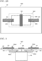
- FIG. 2A is a partial side view and FIG. 2B is a partial plan view showing the power conversion device according to embodiment 1.
- FIG. 2A and 2B show the periphery of a main circuit component 400 in the power conversion device 1000, as viewed from the side and top thereof, respectively.
- the main circuit component 400 shown in FIG. 2A and 2B represents one or any combination of the various main circuit components shown in FIG. 1 , i.e., the reactor 401, the capacitor 402, the transformer 403, or the reactor 404.
- the main circuit wire 200 is wired so as to be divided into a first main circuit wire 201 and a second main circuit wire 202 on a substrate 100 as illustrated in the drawings, and the first main circuit wire 201 and the second main circuit wire 202 are wired so as to be separated from each other in the plane direction of the substrate 100.
- the control wire 300 is wired between the first main circuit wire 201 and the second main circuit wire 202, and the first main circuit wire 201 and the second main circuit wire 202 are insulated from the control wire 300.
- the substrate 100 may be a single-layer wiring substrate or a multi-layer wiring substrate.
- the control wire 300 has one end connected to a control connector which is connected to an external device and the other end connected to a control circuit and a voltage/current detection circuit.
- the main circuit component 400 is mounted directly below the control wire 300 in FIG. 2A , and is placed at a position separated from the substrate 100 by a predetermined distance L in the thickness direction of the substrate 100. That is, the main circuit component 400 is placed so as to be separated from the control wire 300 in the thickness direction of the substrate 100.
- a plate-shaped metal member 500 which is grounded and has holes (not shown) through which a terminal 400a and a terminal 400b described later pass, is provided between the substrate 100 and the main circuit component 400, and a surface of the main circuit component 400 which faces the substrate 100 is covered by the plate-shaped metal member 500. As shown in FIG.
- the area of a projection plane 500A of the metal member 500 on the substrate 100 is larger than the area of a projection plane 400A of the main circuit component 400 such that the projection plane 400A of the main circuit component 400 is included within the projection plane 500A of the metal member 500.
- the metal member 500 is made in contact with the main circuit component 400.
- the metal member 500 may be separated from the main circuit component 400.
- the distance L may be several centimeters, although the distance depends on the lengths of the terminals of the main circuit component described later.
- the main circuit component 400 is connected to the first main circuit wire 201 and the second main circuit wire 202 via the terminal 400a and the terminal 400b respectively provided at one end and another end in the plane direction of the substrate 100.
- the main circuit component 400 corresponds to a main circuit wire connecting part.
- the terminal 400a and the terminal 400b extend toward the substrate 100 from a surface of the main circuit component 400 which faces the substrate 100, and are connected to the first main circuit wire 201 and the second main circuit wire 202, respectively, through the holes (not shown) formed in the substrate 100.
- the first main circuit wire 201 and the second main circuit wire 202 are respectively wired in accordance with the positions of the terminal 400a and the terminal 400b, and a part of each wire overlaps the projection plane 400A.
- the main circuit component 400 is mounted directly below the control wire 300, a part of the control wire 300 overlaps the projection plane 400A.
- the first main circuit wire 201, the second main circuit wire 202, and the control wire 300 are respectively arranged so as to partially overlap the projection plane 400A.
- these wires may be each arranged so as to entirely overlap the projection plane 400A.
- the terminal 400a and the terminal 400b are provided respectively at the one end and the other end in the plane direction of the substrate 100, and the first main circuit wire 201 and the second main circuit wire 202 are respectively wired in accordance with the positions of the terminal 400a and the terminal 400b of the main circuit component 400.
- the distance between the first main circuit wire 201 and the second main circuit wire 202 is approximately equal to the projection plane 400A. Accordingly, the larger the projection plane 400A of the main circuit component 400 is, the larger the area between the first main circuit wire 201 and the second main circuit wire 202 becomes.
- the main circuit component 400 includes large components such as the transformer 403 and the reactors 401, 404 and thus the projection plane 400A is larger, the area between the first main circuit wire 201 and the second main circuit wire 202 becomes larger and the area where the control wire 300 can be wired also becomes larger.
- the terminals 400a and 400b are placed on a surface of the main circuit component 400 which faces the substrate 100.
- L-shaped terminals that bend toward the substrate 100 may be provided on side surfaces of the main circuit component 400.
- the terminals for connecting between the main circuit component 400, and the first main circuit wire 201 and the second main circuit wire 202, respectively, are provided at the one end and the other end of the main circuit component 400 in the plane direction of the substrate 100, such that an area where the control wire 300 can be wired is formed between the first main circuit wire 201 and the second main circuit wire 202.
- the main circuit component 400 is used as a main circuit wire connecting part.
- a bus bar may be used for connecting the first main circuit wire 201 and the second main circuit wire 202.
- the control wire 300 is wired, but also a control component connected to the control wire 300 may be placed.
- the generation of noise due to coupling can be suppressed and the size of the substrate can be reduced. More specifically, on the substrate, the first main circuit wire and the second main circuit wire which configure a main circuit wire are wired so as to be separated from each other, and the control wire is wired between the first main circuit wire and the second main circuit wire.
- the main circuit component is placed so as to be separated from the control wire in the thickness direction of the substrate, and the first main circuit wire and the second main circuit wire are connected to each other via the main circuit component.
- the first main circuit wire or the second main circuit wire it is not necessary to cause the first main circuit wire or the second main circuit wire to cross the control wire in order to connect the first main circuit wire and the second main circuit wire, and thus, the generation of noise due to coupling between the main circuit wire and the control wire can be suppressed.
- the first main circuit wire and the second main circuit wire need not take a detour to avoid the control wire, the increase in size of the substrate due to the detour of the wire can be prevented, thereby achieving the size reduction.
- any coil and capacitor for noise cutting are not required, thereby achieving the size reduction and cost reduction of the power conversion device as a whole.
- the substrate and the main circuit component are placed so as to be separated from each other by a predetermined distance in the thickness direction of the substrate, it is possible to more assuredly suppress coupling between the control wire, and the main circuit wire and the main circuit component.
- the grounded plate-shaped metal member is placed between the main circuit component and the substrate, it is possible to further assuredly suppress coupling between the control wire, and the main circuit wire and the main circuit component, by a shielding effect.
- the projection plane of the main circuit component on the substrate is included within the projection plane of the plate-shaped metal member on the substrate, a surface of the main circuit component which faces the substrate is entirely covered by the plate-shaped metal member. Accordingly, a shielding effect can be obtained over the entire main circuit component.
- the main circuit component includes large components such as a reactor or a transformer
- the area between the first main circuit wire and the second main circuit wire becomes larger and the area where the control wire can be wired also becomes larger. Accordingly, it becomes possible to wire the control wire between the first main circuit wire and the second main circuit wire in a concentrated manner, thereby allowing further size reduction of the substrate.
- the degree of freedom in wiring of the control wire in the projection plane of the main circuit component may be increased by changing the routing of the terminals of the main circuit component and designing a connecting point between the first main circuit wire and the second main circuit wire. In this case, further size reduction of the substrate 100 becomes possible.
- FIG. 3 is a partial side view showing a power conversion device according to embodiment 2.
- FIG. 3 shows the periphery of an arbitrary main circuit component 400 of a power conversion device 1010 corresponding to the power conversion device 1000 in embodiment 1, as viewed from the side thereof.
- terminals for connecting the main circuit component, and the first main circuit wire and the second main circuit wire are each divided into two divided terminals.
- the main circuit component 400 is provided with a first divided terminal 400a1 and a first divided terminal 400b1 at one end and another end in the plane direction of the substrate 100.
- the first divided terminal 400a1 and the first divided terminal 400b1 extend toward the substrate 100 and are respectively connected to lower surfaces, i.e., surfaces facing the main circuit component 400, of conductive intermediate members 601 and 602 placed between the metal member 500 and the substrate 100.
- a second divided terminal 400a2 and a second divided terminal 400b2 passing through holes (not shown) formed in the substrate 100 and respectively connected to the first main circuit wire 201 and the second main circuit wire 202, are respectively connected to upper surfaces, i.e., surfaces facing the substrate 100, of the intermediate members 601 and 602.
- the intermediate member 601 is a plate-shaped or bar-shaped conductive member that extends from the control wire 300 side to the first main circuit wire 201 side along the plane direction of the substrate 100.
- a connecting position between the intermediate member 601 and the second divided terminal 400a2 is placed on the outer side of the connecting position between the intermediate member 601 and the first divided terminal 400a1, that is, on the side closer to the first main circuit wire 201.
- the intermediate member 602 is a plate-shaped or bar-shaped conductive member that extends from the control wire 300 side to the second main circuit wire 202 side along the plane direction of the substrate 100.
- a connecting position between the intermediate member 602 and the second divided terminal 400b2 is placed on the outer side of the connecting position between the intermediate member 602 and the first divided terminal 400a1, that is, on the side closer to the second main circuit wire 202. Therefore, the first main circuit wire 201 and the second main circuit wire 202 are respectively wired in accordance with the positions of the second divided terminals 400a2 and 400b2. Accordingly, the main circuit component 400 is connected to the first main circuit wire 201 via the first divided terminal 400a1, the intermediate member 601, and the second divided terminal 400a2, and is connected to the second main circuit wire 202 via the first divided terminal 400b1, the intermediate member 602, and the second divided terminal 400b2.
- the first divided terminal 400a1, the intermediate member 601, and the second divided terminal 400a2 correspond to the terminal 400a in embodiment 1
- the first divided terminal 400b1, the intermediate member 602, and the second divided terminal 400b2 correspond to the terminal 400b in embodiment 1.
- the other components are the same as those in embodiment 1 and therefore the description thereof is omitted.
- the same effects as in embodiment 1 can be obtained.
- the terminals for connecting the main circuit component, and the first main circuit wire and the second main circuit wire are divided into the first divided terminals connected to the main circuit component, and the second divided terminals connected to the first main circuit wire and the second main circuit wire, and each first divided terminal and each second divided terminal are electrically connected via a conductive intermediate member.
- the connecting position between the second divided terminal and the intermediate member is set on the outer side of the connecting position between the first divided terminal and the intermediate member. Therefore, even when the size of the main circuit component is small and the distance between the first divided terminals is short, the distance between the second divided terminals can be made longer, and thus, the area between the first main circuit wire and the second main circuit wire can be made larger.
- the terminals for connecting the main circuit component, and the first main circuit wire and the second main circuit wire are each divided into two divided terminals. However, each terminal may be divided into three or more divided terminals.
Landscapes
- Engineering & Computer Science (AREA)
- Power Engineering (AREA)
- Microelectronics & Electronic Packaging (AREA)
- Physics & Mathematics (AREA)
- Electromagnetism (AREA)
- Dc-Dc Converters (AREA)
- Inverter Devices (AREA)
Abstract
Description
- The present disclosure relates to a power conversion device.
- In recent years, the higher-frequency driving of a power conversion device has been promoted, and wide-gap semiconductors such as Silicon Carbide (SiC) and Gallium Nitride (GaN) are used as switching elements of inverter circuits. The higher-frequency driving of a power conversion device has advantages that enable high-speed control such as real-time control, but also has disadvantages including the increase in heat generated in semiconductor switching elements due to the increase in switching loss, and the increase in heat generated in electrical components such as a reactor and a transformer due to the increase in copper loss and iron loss.
- In response to this, a power conversion device is proposed, the power conversion device including a recess for housing an electrical component therein, a cover having a semiconductor switching element to be mounted on a flat surface on the surface side thereof, and a case having a cooling flow passage formed so as to allow a refrigerant to flow through a side surface of the recess (see Patent Document 1, for example). In the power conversion device in Patent Document 1, a circuit board is fixed to the surface side of the cover.
- Patent Document 1:
Japanese Patent No. 5823020 - In the power conversion device in Patent Document 1, the circuit board is fixed to the upper side of the cover and the case, and a main circuit wire and a control wire are wired on a single circuit board. When the main circuit wire and the control wire are wired on a single circuit board, it is necessary to cause one of the wires to take a detour depending on the positional relationship between the main circuit wire and the control wire to prevent contact therebetween, which may lead to an increase in substrate area and size increase of the power conversion device. It is conceivable that the positions of an input connector, an output connector, and a control connector for establishing a connection with peripheral devices, are improved (for example, such that the control connector is not placed between the input connector and the output connector) so as to prevent a wire from taking a detour. However, as in the case of an on-vehicle power conversion device, for example, the positions of connectors for establishing a connection with peripheral devices may be limited. Furthermore, it is possible to wire a control wire and a main circuit wire in different wiring layers by using a multi-layer wiring substrate such that the wires cross each other, so as to prevent the wires from taking a detour. However, at the position where the wires cross each other, noise occurs due to coupling between the control wire and the main circuit wire. The noise due to coupling can be eliminated by a noise filter. However, a coil or a capacitor should be added to form a noise filter, which increases the size of a power conversion device. Accordingly, in conventional power conversion devices, it is difficult to achieve the suppression of the generation of noise due to coupling and the reduction of the size of a substrate, simultaneously.
- The present disclosure has been made to solve the above problem, and an object of the present disclosure is to obtain a power conversion device that can suppress the generation of noise due to coupling and reduce the size of a substrate.
- A power conversion device according to the present disclosure includes a main circuit wire for connecting a main circuit component and a plurality of switching elements so as to configure a main circuit, and a control wire for connecting the plurality of switching elements and a control circuit for controlling driving of the plurality of switching elements, the main circuit wire and the control wire being wired on a single substrate, wherein the main circuit wire includes a first main circuit wire and a second main circuit wire wired so as to be separated from each other on the substrate, the control wire is wired between the first main circuit wire and the second main circuit wire on the substrate, and the first main circuit wire and the second main circuit wire are connected via a main circuit wire connecting part placed so as to be separated from the control wire in a thickness direction of the substrate.
- A power conversion device according to the present disclosure can suppress the generation of noise due to coupling and reduce the size of a substrate.
-
- [
FIG. 1] FIG. 1 is a schematic circuit diagram showing a power conversion device according to embodiment 1. - [
FIG. 2A] FIG. 2A is a partial side view showing the power conversion device according to embodiment 1. - [
FIG. 2B] FIG. 2B is a partial plan view showing the power conversion device according to embodiment 1. - [
FIG. 3] FIG. 3 is a partial side view showing a power conversion device according to embodiment 2. - Hereinafter, embodiment 1 will be described on the basis of
FIGS. 1 to 2B .FIG. 1 is a schematic circuit diagram showing a power conversion device according to embodiment 1. Apower conversion device 1000 converts AC power outputted from anAC power supply 901 to DC power having a desired voltage and supplies the resultant DC power to aload 902, and includes amain circuit 900 in which current from theAC power supply 901 flows, and acontrol circuit 903 which controls driving of a plurality of switching elements S11 to S14 provided in themain circuit 900. The plurality of switching elements S11 to S14 and various main circuit components are connected to one another throughmain circuit wires 200 so as to form themain circuit 900. Additionally, the plurality of switching elements S11 to S14 and thecontrol circuit 903 are connected viarespective control wires 300 which are electrically insulated from themain circuit wires 200. Note that the "main circuit components" in embodiment 1 are areactor 401, acapacitor 402, atransformer 403, and areactor 404, but are not limited thereto and include all electrical components which form the main circuit in the power conversion device, as well as a combination thereof. - The
main circuit 900 is configured by the primary side to which theAC power supply 901 is connected and the secondary side to which theload 902 is connected, and includes: arectifier 911 which rectifies AC current outputted from theAC power supply 901; thecapacitor 402 which smooths the current rectified by therectifier 911 and outputs DC voltage; aninverter unit 912 which converts the DC voltage outputted from thecapacitor 402 to AC voltage having a desired frequency and outputs the resultant AC voltage to a primary coil of thetransformer 403; thetransformer 403 which changes the voltage value of the AC voltage from theinverter unit 912 to a desired value and outputs the resultant AC voltage from a secondary coil; arectifier 913 which rectifies current flowing by the AC voltage from thetransformer 403; and thereactor 404 which smooths the current rectified by therectifier 913 and outputs the DC current to theload 902. - The
rectifier 911 is configured by a series-connected assembly of a diode D11 and a diode D12, and a series-connected assembly of a diode D13 and a diode D14, which are connected in parallel to each other. One end of theAC power supply 901 is connected to a connecting point between the diode D11 and the diode D12 via thesmoothing reactor 401 and the other end of theAC power supply 901 is connected to a connecting point between the diode D13 and the diode D14. - The
capacitor 402 may be a film capacitor and an aluminum electrolytic capacitor, for example, and is connected in parallel between therectifier 911 and theinverter unit 912. - The
inverter unit 912 is configured by bridge-connecting the plurality of switching elements S11 to S14, which are Insulated Gate Bipolar Transistors (IGBT) using wide-gap semiconductors such as SiC and GaN, for example. The switching elements S11 to S14 have respective base terminals connected to thecontrol circuit 903 via thecontrol wires 300. Thecontrol circuit 903 generates control signals corresponding to the respective switching elements, and controls driving of the switching elements by transmitting the control signals via thecontrol wires 300. IGBTs are used as the switching elements S11 to S14 in the present disclosure, but other semiconductor switching elements such as Metal-Oxide-Semiconductor Field-Effect Transistors (MOSFET) may be used. - The
transformer 403 is configured by winding, around a magnetic core (not shown) such as an iron core, a primary coil connected to the primary side of themain circuit 900 and a secondary coil connected to the secondary side of themain circuit 900 and polarized in the same direction as the primary coil, and electrically insulates the primary side and the secondary side of themain circuit 900 from each other. The primary coil and the secondary coil of thetransformer 403 are magnetically connected by the magnetic core such that magnetic flux generated by AC current flowing through the primary coil is transmitted to the secondary coil via the magnetic core, and the magnetic flux generates an induced electromotive force in the secondary coil and then, the secondary coil outputs AC voltage to therectifier 913. The magnitude of the AC voltage outputted from the secondary coil to therectifier 913 is adjusted to a desired value by adjusting the turns ratio between the primary coil and the secondary coil of thetransformer 403. - The
rectifier 913 is configured by a series-connected assembly of a diode D21 and a diode D22, and a series-connected assembly of a diode D23 and a diode D24, which are connected in parallel to each other. One end of the secondary coil of thetransformer 403 is connected to a connecting point between the diode D21 and the diode D22 and the other end thereof is connected to a connecting point between the diode D23 and the diode D24. - The
reactor 404 is connected in series between therectifier 913 and theload 902 so as to perform smoothing by eliminating pulsations from the current outputted from therectifier 913. - The
load 902 may be a battery, and one end thereof is connected to thereactor 404 and the other end thereof is connected to an anode terminal of the diode D24. - Note that the power conversion device shown in
FIG. 1 is merely one example, and not limited thereto. For example, the power conversion device may be a DC-DC converter. In other words, the power conversion device can be any device which controls driving of switching elements connected to a main circuit by a control circuit so as to convert input power to desired power and output the resultant power. - Next, wiring of the
main circuit wire 200 and thecontrol wire 300 will be described.FIG. 2A is a partial side view andFIG. 2B is a partial plan view showing the power conversion device according to embodiment 1.FIG. 2A and2B show the periphery of amain circuit component 400 in thepower conversion device 1000, as viewed from the side and top thereof, respectively. Themain circuit component 400 shown inFIG. 2A and2B represents one or any combination of the various main circuit components shown inFIG. 1 , i.e., thereactor 401, thecapacitor 402, thetransformer 403, or thereactor 404. Themain circuit wire 200 is wired so as to be divided into a firstmain circuit wire 201 and a secondmain circuit wire 202 on asubstrate 100 as illustrated in the drawings, and the firstmain circuit wire 201 and the secondmain circuit wire 202 are wired so as to be separated from each other in the plane direction of thesubstrate 100. Thecontrol wire 300 is wired between the firstmain circuit wire 201 and the secondmain circuit wire 202, and the firstmain circuit wire 201 and the secondmain circuit wire 202 are insulated from thecontrol wire 300. Note that thesubstrate 100 may be a single-layer wiring substrate or a multi-layer wiring substrate. Although not shown, thecontrol wire 300 has one end connected to a control connector which is connected to an external device and the other end connected to a control circuit and a voltage/current detection circuit. - The
main circuit component 400 is mounted directly below thecontrol wire 300 inFIG. 2A , and is placed at a position separated from thesubstrate 100 by a predetermined distance L in the thickness direction of thesubstrate 100. That is, themain circuit component 400 is placed so as to be separated from thecontrol wire 300 in the thickness direction of thesubstrate 100. A plate-shapedmetal member 500 which is grounded and has holes (not shown) through which aterminal 400a and a terminal 400b described later pass, is provided between thesubstrate 100 and themain circuit component 400, and a surface of themain circuit component 400 which faces thesubstrate 100 is covered by the plate-shapedmetal member 500. As shown inFIG. 2B , the area of aprojection plane 500A of themetal member 500 on thesubstrate 100 is larger than the area of aprojection plane 400A of themain circuit component 400 such that theprojection plane 400A of themain circuit component 400 is included within theprojection plane 500A of themetal member 500. In embodiment 1, themetal member 500 is made in contact with themain circuit component 400. However, as long as themetal member 500 is placed between thesubstrate 100 and themain circuit component 400, themetal member 500 may be separated from themain circuit component 400. The distance L may be several centimeters, although the distance depends on the lengths of the terminals of the main circuit component described later. - The
main circuit component 400 is connected to the firstmain circuit wire 201 and the secondmain circuit wire 202 via theterminal 400a and the terminal 400b respectively provided at one end and another end in the plane direction of thesubstrate 100. By connecting the firstmain circuit wire 201 and the secondmain circuit wire 202 to themain circuit component 400 as described above, the firstmain circuit wire 201 and the secondmain circuit wire 202 are connected via themain circuit component 400. In other words, themain circuit component 400 corresponds to a main circuit wire connecting part. The terminal 400a and the terminal 400b extend toward thesubstrate 100 from a surface of themain circuit component 400 which faces thesubstrate 100, and are connected to the firstmain circuit wire 201 and the secondmain circuit wire 202, respectively, through the holes (not shown) formed in thesubstrate 100. Therefore, the firstmain circuit wire 201 and the secondmain circuit wire 202 are respectively wired in accordance with the positions of the terminal 400a and the terminal 400b, and a part of each wire overlaps theprojection plane 400A. In addition, since themain circuit component 400 is mounted directly below thecontrol wire 300, a part of thecontrol wire 300 overlaps theprojection plane 400A. In embodiment 1, the firstmain circuit wire 201, the secondmain circuit wire 202, and thecontrol wire 300 are respectively arranged so as to partially overlap theprojection plane 400A. However, these wires may be each arranged so as to entirely overlap theprojection plane 400A. - As described above, the terminal 400a and the terminal 400b are provided respectively at the one end and the other end in the plane direction of the
substrate 100, and the firstmain circuit wire 201 and the secondmain circuit wire 202 are respectively wired in accordance with the positions of the terminal 400a and the terminal 400b of themain circuit component 400. Thus, the distance between the firstmain circuit wire 201 and the secondmain circuit wire 202 is approximately equal to theprojection plane 400A. Accordingly, the larger theprojection plane 400A of themain circuit component 400 is, the larger the area between the firstmain circuit wire 201 and the secondmain circuit wire 202 becomes. Thus, when themain circuit component 400 includes large components such as thetransformer 403 and thereactors projection plane 400A is larger, the area between the firstmain circuit wire 201 and the secondmain circuit wire 202 becomes larger and the area where thecontrol wire 300 can be wired also becomes larger. - In embodiment 1, the
terminals main circuit component 400 which faces thesubstrate 100. However, as long as the distance between the firstmain circuit wire 201 and the secondmain circuit wire 202 is approximately equal to the width of theprojection plane 400A, L-shaped terminals that bend toward thesubstrate 100 may be provided on side surfaces of themain circuit component 400. In other words, it is sufficient that the terminals for connecting between themain circuit component 400, and the firstmain circuit wire 201 and the secondmain circuit wire 202, respectively, are provided at the one end and the other end of themain circuit component 400 in the plane direction of thesubstrate 100, such that an area where thecontrol wire 300 can be wired is formed between the firstmain circuit wire 201 and the secondmain circuit wire 202. - In embodiment 1, the
main circuit component 400 is used as a main circuit wire connecting part. However, for example, a bus bar may be used for connecting the firstmain circuit wire 201 and the secondmain circuit wire 202. In addition, in the area between the firstmain circuit wire 201 and the secondmain circuit wire 202, not only thecontrol wire 300 is wired, but also a control component connected to thecontrol wire 300 may be placed. - According to embodiment 1, the generation of noise due to coupling can be suppressed and the size of the substrate can be reduced. More specifically, on the substrate, the first main circuit wire and the second main circuit wire which configure a main circuit wire are wired so as to be separated from each other, and the control wire is wired between the first main circuit wire and the second main circuit wire. The main circuit component is placed so as to be separated from the control wire in the thickness direction of the substrate, and the first main circuit wire and the second main circuit wire are connected to each other via the main circuit component. Therefore, it is not necessary to cause the first main circuit wire or the second main circuit wire to cross the control wire in order to connect the first main circuit wire and the second main circuit wire, and thus, the generation of noise due to coupling between the main circuit wire and the control wire can be suppressed. In addition, since the first main circuit wire and the second main circuit wire need not take a detour to avoid the control wire, the increase in size of the substrate due to the detour of the wire can be prevented, thereby achieving the size reduction. Furthermore, any coil and capacitor for noise cutting are not required, thereby achieving the size reduction and cost reduction of the power conversion device as a whole.
- Since the substrate and the main circuit component are placed so as to be separated from each other by a predetermined distance in the thickness direction of the substrate, it is possible to more assuredly suppress coupling between the control wire, and the main circuit wire and the main circuit component.
- Since the grounded plate-shaped metal member is placed between the main circuit component and the substrate, it is possible to further assuredly suppress coupling between the control wire, and the main circuit wire and the main circuit component, by a shielding effect.
- Since the projection plane of the main circuit component on the substrate is included within the projection plane of the plate-shaped metal member on the substrate, a surface of the main circuit component which faces the substrate is entirely covered by the plate-shaped metal member. Accordingly, a shielding effect can be obtained over the entire main circuit component.
- In a case where the main circuit component includes large components such as a reactor or a transformer, the area between the first main circuit wire and the second main circuit wire becomes larger and the area where the control wire can be wired also becomes larger. Accordingly, it becomes possible to wire the control wire between the first main circuit wire and the second main circuit wire in a concentrated manner, thereby allowing further size reduction of the substrate.
- Note that the degree of freedom in wiring of the control wire in the projection plane of the main circuit component may be increased by changing the routing of the terminals of the main circuit component and designing a connecting point between the first main circuit wire and the second main circuit wire. In this case, further size reduction of the
substrate 100 becomes possible. - Hereinafter, embodiment 2 will be discussed on the basis of
FIG. 3 . The components identical to or corresponding to those inFIGS. 1 to 2B are denoted by the same reference characters and the description thereof is omitted.FIG. 3 is a partial side view showing a power conversion device according to embodiment 2.FIG. 3 shows the periphery of an arbitrarymain circuit component 400 of apower conversion device 1010 corresponding to thepower conversion device 1000 in embodiment 1, as viewed from the side thereof. In embodiment 2, terminals for connecting the main circuit component, and the first main circuit wire and the second main circuit wire, are each divided into two divided terminals. - The
main circuit component 400 is provided with a first divided terminal 400a1 and a first divided terminal 400b1 at one end and another end in the plane direction of thesubstrate 100. The first divided terminal 400a1 and the first divided terminal 400b1 extend toward thesubstrate 100 and are respectively connected to lower surfaces, i.e., surfaces facing themain circuit component 400, of conductiveintermediate members metal member 500 and thesubstrate 100. A second divided terminal 400a2 and a second divided terminal 400b2 passing through holes (not shown) formed in thesubstrate 100 and respectively connected to the firstmain circuit wire 201 and the secondmain circuit wire 202, are respectively connected to upper surfaces, i.e., surfaces facing thesubstrate 100, of theintermediate members - The
intermediate member 601 is a plate-shaped or bar-shaped conductive member that extends from thecontrol wire 300 side to the firstmain circuit wire 201 side along the plane direction of thesubstrate 100. A connecting position between theintermediate member 601 and the second divided terminal 400a2 is placed on the outer side of the connecting position between theintermediate member 601 and the first divided terminal 400a1, that is, on the side closer to the firstmain circuit wire 201. Theintermediate member 602 is a plate-shaped or bar-shaped conductive member that extends from thecontrol wire 300 side to the secondmain circuit wire 202 side along the plane direction of thesubstrate 100. A connecting position between theintermediate member 602 and the second divided terminal 400b2 is placed on the outer side of the connecting position between theintermediate member 602 and the first divided terminal 400a1, that is, on the side closer to the secondmain circuit wire 202. Therefore, the firstmain circuit wire 201 and the secondmain circuit wire 202 are respectively wired in accordance with the positions of the second divided terminals 400a2 and 400b2. Accordingly, themain circuit component 400 is connected to the firstmain circuit wire 201 via the first divided terminal 400a1, theintermediate member 601, and the second divided terminal 400a2, and is connected to the secondmain circuit wire 202 via the first divided terminal 400b1, theintermediate member 602, and the second divided terminal 400b2. In other words, the first divided terminal 400a1, theintermediate member 601, and the second divided terminal 400a2 correspond to the terminal 400a in embodiment 1, and the first divided terminal 400b1, theintermediate member 602, and the second divided terminal 400b2 correspond to the terminal 400b in embodiment 1. The other components are the same as those in embodiment 1 and therefore the description thereof is omitted. - According to embodiment 2, the same effects as in embodiment 1 can be obtained. In addition, even when the size of the main circuit component is small, the area between the first main circuit wire and the second main circuit wire is enlarged, whereby an area for wiring the control wire can be ensured. More specifically, the terminals for connecting the main circuit component, and the first main circuit wire and the second main circuit wire, are divided into the first divided terminals connected to the main circuit component, and the second divided terminals connected to the first main circuit wire and the second main circuit wire, and each first divided terminal and each second divided terminal are electrically connected via a conductive intermediate member. Here, the connecting position between the second divided terminal and the intermediate member is set on the outer side of the connecting position between the first divided terminal and the intermediate member. Therefore, even when the size of the main circuit component is small and the distance between the first divided terminals is short, the distance between the second divided terminals can be made longer, and thus, the area between the first main circuit wire and the second main circuit wire can be made larger.
- In embodiment 2, the terminals for connecting the main circuit component, and the first main circuit wire and the second main circuit wire, are each divided into two divided terminals. However, each terminal may be divided into three or more divided terminals.
- Although the disclosure is described above in terms of various exemplary embodiments and implementations, it should be understood that the various features, aspects and functionality described in one or more of the individual embodiments are not limited in their applicability to the particular embodiment with which they are described, but instead can be applied, alone or in various combinations to one or more of the embodiments of the disclosure.
- It is therefore understood that numerous modifications which have not been exemplified can be devised without departing from the scope of the present disclosure. For example, at least one of the constituent components may be modified, added, or eliminated. At least one of the constituent components mentioned in at least one of the preferred embodiments may be selected and combined with the constituent components mentioned in another preferred embodiment.
-
- 100
- substrate
- 200
- main circuit wire
- 201
- first main circuit wire
- 202
- second main circuit wire
- 300
- control wire
- 400
- main circuit component
- 400a, 400b
- terminal
- 400a1, 400b1
- first divided terminal
- 400a2, 400b2
- second divided terminal
- 400A
- projection plane
- 401
- reactor
- 402
- capacitor
- 403
- transformer
- 404
- reactor
- 500
- metal member
- 500A
- projection plane
- 601, 602
- intermediate member
- 900
- main circuit
- 901
- AC power supply
- 902
- load
- 903
- control circuit
- 911, 913
- rectifier
- 912
- inverter unit
- 1000, 1010
- power conversion device
- D11 to D14, D21 to D24
- diode
- S11 to S14
- switching element
Claims (7)
- A power conversion device comprising a main circuit wire for connecting a main circuit component and a plurality of switching elements so as to configure a main circuit, and a control wire for connecting the plurality of switching elements and a control circuit for controlling driving of the plurality of switching elements, the main circuit wire and the control wire being wired on a single substrate, whereinthe main circuit wire includes a first main circuit wire and a second main circuit wire wired so as to be separated from each other on the substrate,the control wire is wired between the first main circuit wire and the second main circuit wire on the substrate, andthe first main circuit wire and the second main circuit wire are connected via a main circuit wire connecting part placed so as to be separated from the control wire in a thickness direction of the substrate.
- The power conversion device according to claim 1, wherein
the main circuit wire connecting part is placed so as to be separated from the substrate by a predetermined distance in the thickness direction of the substrate. - The power conversion device according to claim 2, wherein
a grounded plate-shaped metal member is placed between the main circuit wire connecting part and the substrate. - The power conversion device according to claim 3, wherein
a projection plane of the main circuit wire connecting part on the substrate is included within a projection plane of the metal member on the substrate. - The power conversion device according to any one of claims 1 to 4, wherein
the main circuit wire connecting part is the main circuit component. - The power conversion device according to claim 5, whereinterminals for connecting the main circuit component, and the first main circuit wire and the second main circuit wire, are composed of first divided terminals connected to the main circuit component, second divided terminals connected to the first main circuit wire and the second main circuit wire, and conductive intermediate members for electrically connecting the first divided terminals and the second divided terminals, andconnecting positions between the second divided terminals and the intermediate members are placed on the outer sides of connecting positions between the first divided terminals and the intermediate members.
- The power conversion device according to claim 5 or 6, wherein
the main circuit component includes a reactor or a transformer.
Applications Claiming Priority (2)
| Application Number | Priority Date | Filing Date | Title |
|---|---|---|---|
| JP2018206247A JP6541859B1 (en) | 2018-11-01 | 2018-11-01 | Power converter |
| PCT/JP2019/007995 WO2020090131A1 (en) | 2018-11-01 | 2019-03-01 | Power conversion device |
Publications (2)
| Publication Number | Publication Date |
|---|---|
| EP3876408A1 true EP3876408A1 (en) | 2021-09-08 |
| EP3876408A4 EP3876408A4 (en) | 2021-12-22 |
Family
ID=67212135
Family Applications (1)
| Application Number | Title | Priority Date | Filing Date |
|---|---|---|---|
| EP19878757.4A Pending EP3876408A4 (en) | 2018-11-01 | 2019-03-01 | POWER CONVERSION DEVICE |
Country Status (5)
| Country | Link |
|---|---|
| US (1) | US11509236B2 (en) |
| EP (1) | EP3876408A4 (en) |
| JP (1) | JP6541859B1 (en) |
| CN (1) | CN112913132B (en) |
| WO (1) | WO2020090131A1 (en) |
Families Citing this family (2)
| Publication number | Priority date | Publication date | Assignee | Title |
|---|---|---|---|---|
| JP7098025B1 (en) * | 2021-06-09 | 2022-07-08 | 三菱電機株式会社 | Power converter |
| JP7724748B2 (en) | 2022-05-25 | 2025-08-18 | 三菱電機株式会社 | air conditioning equipment |
Family Cites Families (15)
| Publication number | Priority date | Publication date | Assignee | Title |
|---|---|---|---|---|
| NL6717634A (en) * | 1967-12-22 | 1969-06-24 | ||
| JPS5823020B2 (en) | 1978-03-13 | 1983-05-12 | 三洋電機株式会社 | Radio receiver reception frequency display circuit |
| US4816984A (en) * | 1987-02-06 | 1989-03-28 | Siemens Aktiengesellschaft | Bridge arm with transistors and recovery diodes |
| US5031069A (en) * | 1989-12-28 | 1991-07-09 | Sundstrand Corporation | Integration of ceramic capacitor |
| JP3055302B2 (en) * | 1992-04-24 | 2000-06-26 | 三菱電機株式会社 | Semiconductor device |
| JP3196187B2 (en) * | 1993-05-11 | 2001-08-06 | 横河電機株式会社 | Mounting structure of electromagnetic circuit |
| CN100367645C (en) * | 2003-08-20 | 2008-02-06 | 松下电器产业株式会社 | Switching power supply |
| JP4003719B2 (en) * | 2003-08-22 | 2007-11-07 | 株式会社デンソー | Power converter |
| JP2011019371A (en) * | 2009-07-10 | 2011-01-27 | Sanken Electric Co Ltd | Dc-dc converter |
| JP5669677B2 (en) * | 2011-06-14 | 2015-02-12 | 住友重機械工業株式会社 | Power conversion device and power conversion module |
| EP2830073B1 (en) | 2012-03-19 | 2017-09-13 | Mitsubishi Electric Corporation | Power conversion apparatus |
| JP5763026B2 (en) * | 2012-09-24 | 2015-08-12 | 株式会社東芝 | Semiconductor device |
| JP6476727B2 (en) * | 2014-10-17 | 2019-03-06 | 日産自動車株式会社 | Power supply |
| JP6174824B2 (en) * | 2015-04-20 | 2017-08-02 | 三菱電機株式会社 | Power converter |
| JP2017038017A (en) * | 2015-08-13 | 2017-02-16 | 富士通株式会社 | Noise reducing substrate and electronic equipment |
-
2018
- 2018-11-01 JP JP2018206247A patent/JP6541859B1/en active Active
-
2019
- 2019-03-01 CN CN201980070538.0A patent/CN112913132B/en active Active
- 2019-03-01 EP EP19878757.4A patent/EP3876408A4/en active Pending
- 2019-03-01 WO PCT/JP2019/007995 patent/WO2020090131A1/en not_active Ceased
- 2019-03-01 US US17/263,725 patent/US11509236B2/en active Active
Also Published As
| Publication number | Publication date |
|---|---|
| WO2020090131A1 (en) | 2020-05-07 |
| JP6541859B1 (en) | 2019-07-10 |
| US20210376751A1 (en) | 2021-12-02 |
| EP3876408A4 (en) | 2021-12-22 |
| JP2020072587A (en) | 2020-05-07 |
| CN112913132A (en) | 2021-06-04 |
| US11509236B2 (en) | 2022-11-22 |
| CN112913132B (en) | 2024-07-05 |
Similar Documents
| Publication | Publication Date | Title |
|---|---|---|
| EP3443588B1 (en) | Robust low inductance power module package | |
| US9776514B2 (en) | DC-DC converter | |
| US20190110355A1 (en) | Power circuit device | |
| EP3832862B1 (en) | Power conversion device | |
| JP6488996B2 (en) | Power converter | |
| EP3404819A1 (en) | Power converter | |
| US11509236B2 (en) | Power conversion device | |
| CN115459601A (en) | Power conversion device | |
| JP5894909B2 (en) | DC-DC converter device | |
| US12289048B2 (en) | Semiconductor module | |
| CN117062354A (en) | Voltage regulator module with inductor cooling power stage | |
| EP3611835B1 (en) | Electric power conversion device | |
| CN100490293C (en) | Power conversion apparatus | |
| JP2016144238A (en) | Power converter | |
| US9923473B2 (en) | Power supply apparatus for reducing noise induced in DC wires | |
| JP2013188010A (en) | Insulation type switching power supply device | |
| JP7851262B2 (en) | Power converter | |
| US12525887B2 (en) | Power converter | |
| JP6838297B2 (en) | Power converter | |
| US20260011656A1 (en) | Power semiconductor module with shielding heat sink | |
| US11271489B2 (en) | AC-DC power supply and motor | |
| JP2010034310A (en) | Transformer and power converter | |
| US20230022728A1 (en) | Power supply device, acf converter, and ac adapter | |
| JP6225847B2 (en) | Power supply |
Legal Events
| Date | Code | Title | Description |
|---|---|---|---|
| STAA | Information on the status of an ep patent application or granted ep patent |
Free format text: STATUS: THE INTERNATIONAL PUBLICATION HAS BEEN MADE |
|
| PUAI | Public reference made under article 153(3) epc to a published international application that has entered the european phase |
Free format text: ORIGINAL CODE: 0009012 |
|
| STAA | Information on the status of an ep patent application or granted ep patent |
Free format text: STATUS: REQUEST FOR EXAMINATION WAS MADE |
|
| 17P | Request for examination filed |
Effective date: 20210126 |
|
| AK | Designated contracting states |
Kind code of ref document: A1 Designated state(s): AL AT BE BG CH CY CZ DE DK EE ES FI FR GB GR HR HU IE IS IT LI LT LU LV MC MK MT NL NO PL PT RO RS SE SI SK SM TR |
|
| A4 | Supplementary search report drawn up and despatched |
Effective date: 20211123 |
|
| RIC1 | Information provided on ipc code assigned before grant |
Ipc: H02M 7/00 20060101ALN20211117BHEP Ipc: H02M 5/458 20060101ALN20211117BHEP Ipc: H02M 1/42 20070101ALN20211117BHEP Ipc: H02M 3/00 20060101ALI20211117BHEP Ipc: H02M 7/06 20060101ALI20211117BHEP Ipc: H02M 3/335 20060101ALI20211117BHEP Ipc: H02M 1/00 20060101ALI20211117BHEP Ipc: H05K 1/14 20060101ALI20211117BHEP Ipc: H05K 1/02 20060101ALI20211117BHEP Ipc: H02M 3/28 20060101AFI20211117BHEP |
|
| DAV | Request for validation of the european patent (deleted) | ||
| DAX | Request for extension of the european patent (deleted) | ||
| STAA | Information on the status of an ep patent application or granted ep patent |
Free format text: STATUS: EXAMINATION IS IN PROGRESS |
|
| 17Q | First examination report despatched |
Effective date: 20250314 |