EP3876347A1 - Antenna and communication device - Google Patents
Antenna and communication device Download PDFInfo
- Publication number
- EP3876347A1 EP3876347A1 EP19909525.8A EP19909525A EP3876347A1 EP 3876347 A1 EP3876347 A1 EP 3876347A1 EP 19909525 A EP19909525 A EP 19909525A EP 3876347 A1 EP3876347 A1 EP 3876347A1
- Authority
- EP
- European Patent Office
- Prior art keywords
- slot
- conductive plate
- antenna
- branch
- present disclosure
- Prior art date
- Legal status (The legal status is an assumption and is not a legal conclusion. Google has not performed a legal analysis and makes no representation as to the accuracy of the status listed.)
- Withdrawn
Links
Images






Classifications
-
- H—ELECTRICITY
- H01—ELECTRIC ELEMENTS
- H01Q—ANTENNAS, i.e. RADIO AERIALS
- H01Q13/00—Waveguide horns or mouths; Slot antennas; Leaky-waveguide antennas; Equivalent structures causing radiation along the transmission path of a guided wave
- H01Q13/10—Resonant slot antennas
- H01Q13/106—Microstrip slot antennas
-
- H—ELECTRICITY
- H01—ELECTRIC ELEMENTS
- H01Q—ANTENNAS, i.e. RADIO AERIALS
- H01Q5/00—Arrangements for simultaneous operation of antennas on two or more different wavebands, e.g. dual-band or multi-band arrangements
- H01Q5/30—Arrangements for providing operation on different wavebands
- H01Q5/307—Individual or coupled radiating elements, each element being fed in an unspecified way
- H01Q5/342—Individual or coupled radiating elements, each element being fed in an unspecified way for different propagation modes
- H01Q5/357—Individual or coupled radiating elements, each element being fed in an unspecified way for different propagation modes using a single feed point
- H01Q5/364—Creating multiple current paths
- H01Q5/371—Branching current paths
-
- H—ELECTRICITY
- H01—ELECTRIC ELEMENTS
- H01Q—ANTENNAS, i.e. RADIO AERIALS
- H01Q9/00—Electrically-short antennas having dimensions not more than twice the operating wavelength and consisting of conductive active radiating elements
- H01Q9/04—Resonant antennas
- H01Q9/0407—Substantially flat resonant element parallel to ground plane, e.g. patch antenna
- H01Q9/045—Substantially flat resonant element parallel to ground plane, e.g. patch antenna with particular feeding means
- H01Q9/0457—Substantially flat resonant element parallel to ground plane, e.g. patch antenna with particular feeding means electromagnetically coupled to the feed line
-
- H—ELECTRICITY
- H01—ELECTRIC ELEMENTS
- H01Q—ANTENNAS, i.e. RADIO AERIALS
- H01Q1/00—Details of, or arrangements associated with, antennas
- H01Q1/12—Supports; Mounting means
- H01Q1/22—Supports; Mounting means by structural association with other equipment or articles
- H01Q1/24—Supports; Mounting means by structural association with other equipment or articles with receiving set
- H01Q1/241—Supports; Mounting means by structural association with other equipment or articles with receiving set used in mobile communications, e.g. GSM
- H01Q1/242—Supports; Mounting means by structural association with other equipment or articles with receiving set used in mobile communications, e.g. GSM specially adapted for hand-held use
- H01Q1/243—Supports; Mounting means by structural association with other equipment or articles with receiving set used in mobile communications, e.g. GSM specially adapted for hand-held use with built-in antennas
-
- H—ELECTRICITY
- H01—ELECTRIC ELEMENTS
- H01Q—ANTENNAS, i.e. RADIO AERIALS
- H01Q13/00—Waveguide horns or mouths; Slot antennas; Leaky-waveguide antennas; Equivalent structures causing radiation along the transmission path of a guided wave
- H01Q13/10—Resonant slot antennas
-
- H—ELECTRICITY
- H01—ELECTRIC ELEMENTS
- H01Q—ANTENNAS, i.e. RADIO AERIALS
- H01Q5/00—Arrangements for simultaneous operation of antennas on two or more different wavebands, e.g. dual-band or multi-band arrangements
- H01Q5/30—Arrangements for providing operation on different wavebands
- H01Q5/307—Individual or coupled radiating elements, each element being fed in an unspecified way
- H01Q5/342—Individual or coupled radiating elements, each element being fed in an unspecified way for different propagation modes
- H01Q5/357—Individual or coupled radiating elements, each element being fed in an unspecified way for different propagation modes using a single feed point
Definitions
- the present invention relates to an antenna and a communication device, for example.
- a slot antenna is known as an antenna used in a radio communication device.
- Patent Document 1 For example, a slot antenna is disclosed in Patent Document 1.
- Patent Document 1 USP No. 9166300 Specification
- the slot antenna in Patent Document 1 is small but has a problem that there is a case where impedance matching cannot be achieved at a plurality of resonance frequencies.
- An antenna according to an aspect of the present disclosure may be, for example, an antenna which comprises a conductor plate, wherein: the conductor plate has a slot and a branch slot; the branch slot has one end connected to the slot; and the other end of the branch slot extends along the slot, in a direction toward an antinode of an electric field at a lowest-order resonant frequency of the antenna when viewed from the one end, and is shorted in the conductor plate.
- a communication device may be a communication device which comprises an antenna according to an aspect of the present disclosure.
- a small antenna and a communication device provided with the antenna can be provided, wherein the antenna can achieve impedance matching at a plurality of resonance frequencies.
- an antenna may be an antenna A1 which is provided with a conductive plate a1, wherein: the conductive plate a1 is provided with a slot a2 and a branch slot a3; and the branch slot a3 has one end a31 coupled to the slot a2 and another end a32 extending along the slot a2, in a direction toward an antinode of an electric field at the lowest-order resonance frequency of the antenna A1 when viewed from the end a31, and shorted in the conductive plate a1.
- an antenna according to an aspect of the present disclosure may be an antenna A1 which is provided with a conductive plate a1, wherein: the conductive plate a1 is provided with a slot a2 and a branch slot a3; the slot a2 has one end a21 shorted in the conductive plate a1 and another end a22 opened at an edge of the conductive plate; and the branch slot a3 has one end a31 coupled to the slot a2 and another end a32 extending along the slot a2, in a direction toward the other end a22 of the slot a2 when viewed from the end a31 of the branch slot a3, and shorted in the conductive plate a1.
- an antenna according to an aspect of the present disclosure may be an antenna A1 which is provided with a conductive plate a1, wherein: the conductive plate a1 is provided with a slot a2 and a branch slot a3; the slot a2 has both ends a21 and a22 opened at edges of the conductive plate a1; and the branch slot a3 has one end a31 coupled to the slot a2 and another end a32 extending along the slot a2, in a direction toward nearer one of the openings of the slot a2 when viewed from the one end a31 (in a direction toward the end a22), and shorted in the conductive plate a1.
- an antenna according to an aspect of the present disclosure may be an antenna A1 which is provided with a conductive plate a1, wherein: the conductive plate a1 is provided with a slot a2 and a branch slot a3; the slot a2 has both ends a21 and a22 shorted, respectively, in the conductive plate a1; and the branch slot a3 has one end a31 coupled to the slot a2 and another end a32 extending along the slot a2, in a direction toward a middle point a23 in the slot a2 when viewed from the end a31, and shorted in the conductive plate a1.
- the conductive plate a1 may be formed by only a periphery part of the slot a2 and the branch slot a3.
- the conductive plate a1 may formed by coupling a periphery part of the slot a2 and the branch slot a3 to another part. Owing to the coupling, both parts may be formed in practically the same layer or may be formed in different layers as shown in Fig. 8 .
- slot includes a concept of a shape that one of both ends thereof opens at an edge, a concept of a shape that the both ends thereof open at edges and a concept of a shape that the both ends thereof are not opened at the edges.
- the "antinode of an electric field” represents the maximum point of electric field strength, and "a node of an electric field” represents the minimum point of the electric field strength.
- the antinode of the electric field occurs in the end a22, and the node of the electric field occurs in the end a21.
- the "direction toward an antinode of an electric field at the lowest-order resonance frequency of the antenna A1" is the "direction toward the end a22".
- the antinode of the electric field occur at each of the end a21 and the end a22, and the node of the electric field occurs at the middle point a23.
- the "direction toward an antinode of an electric field at the lowest-order resonance frequency of the antenna A1" is the "direction toward nearer one of the openings of the slot a2 when viewed from the end a31 (in a direction toward the end a22)".
- the antinode of the electric field occurs at the middle point a23, and the node of the electric field occurs at each of the one end a21 and the other end a22. Accordingly, in the aspect according to Fig. 5 , the "direction toward an antinode of an electric field at the lowest-order resonance frequency of the antenna A1" is the "direction toward the middle point a23".
- each of Figs. 9 , 10 and 11 shows an antenna having no branch slot a3.
- a conductive plate a1 is formed by coupling a periphery part of a slot a2 to a part other than the periphery part, wherein by the coupling, both parts may be formed in practically the same layer or may be formed in different layers as shown in Fig. 11 .
- impedance is matched at each of a first resonance frequency and a third resonance frequency but is not matched at a second resonance frequency as shown in Fig. 12 .
- impedance is matched at each of a first resonance frequency, a second resonance frequency and a third resonance frequency as shown in Fig. 13 , for example.
- a small antenna which can achieve impedance matching at a plurality of resonance frequencies can be provided, for example.
- an antenna according to an aspect of the present disclosure may be an antenna A2, wherein: a conductive plate a1 is provided with a passive coupling slot a4; and the passive coupling slot a4 has one end a41 coupled to a slot a2 in proximity of an opening (in proximity of an end a22) and another end a42 shorted in the conductive plate a1.
- only one passive coupling slot a4 may be provided as shown in Fig. 14 .
- a plurality of passive coupling slots a4 may be provided as shown in each of Figs. 15-17 .
- the passive coupling slot a4 contributes to radiation by indirectly feeding from feeding to the slot a2.
- a small antenna which operates at a wider frequency band can be provided, for example.
- an antenna according to an aspect of the present disclosure may be an antenna A3, wherein: a conductive plate a1 is attached to an edge of substrate a5 so as to be practically perpendicular to the substrate a5; and an opening of a slot a2 in the conductive plate a1 is on a side, which is practically perpendicular to the substrate a5, of the conductive plate a1.
- the opening of the slot a2 in the conductive plate a1 may be on a side, which is practically parallel to the substrate a5, of the conductive plate a1.
- a small antenna having better characteristics can be provided.
- an antenna according to an aspect of the present disclosure may be an antenna A4, wherein: a conductive plate a1 is formed so as to be practically perpendicular to a reflection plate a6; and an opening of a slot a2 in the conductive plate a1 is on a side, which is practically perpendicular to the reflection plate a6, of the conductive plate a1.
- the opening of the slot a2 in the conductive plate a1 may be on a side, which is practically parallel to the reflection plate a6, of the conductive plate a6.
- a small antenna having better characteristics can be provided.
- an antenna according to an aspect of the present disclosure may be an antenna A5, wherein: a region, which is adjacent to a first long side of a slot a2, of a conductive plate a1 is fed; and a region, which is adjacent to a second long side of the slot a2, of the conductive plate a1 is grounded.
- Any one of long sides of the slot a2 may be the first long side or the second long side.
- the antenna A5 may be fed by means of a feeding line a7 electrically connected to the region, which is adjacent to the first long side of the slot a2, of the conductive plate a1.
- electrically connected include both of a concept of electrical connection that conductors are directly connected to each other and a concept of electric connection of wireless feeding, such as EM feeding.
- the feeding line a7 may be provided in a layer other than the conductive plate a1 and may be connected to the conductive plate a1 though vias, etc.
- the feeding line a7 may be provided in a layer identical to a layer in which the conductive plate a1 is and may form a coplanar line by further extending along a clearance provided in the conductive plate a1.
- the feeding line a7 may be formed with an electrical wire such as a transmission line or by a metal plate.
- the conductive plate a1 and a metal plate part of the feeding line a7 may be formed by cutting out from a conductive plate using laser, etc.
- the feeding line a7 may be formed with a coaxial cable as shown in each of Figs. 21 and 22 .
- a core wire a71 of the coaxial cable may be electrically connected to a region, which is adjacent to a first long side of a slot a2, of a conductive plate a1 by means of soldering, etc. as shown in Fig. 21 , and a connecting aspect may use an auxiliary conductor and a via as shown in Fig. 22 , for example.
- an outer conductor a72 of the coaxial cable may be electrically connected to the conductive plate a1 by means of soldering, etc. so that a region, which is adjacent to a second long side of the slot a2, of the conductive plate a1 as shown in Fig. 21 , and a connecting aspect may use an auxiliary conductor and vias as shown in Fig. 22 , for example.
- an antenna according to an aspect of the present disclosure may be an antenna A6 which is provided with stubs a8 formed in a layer different from a layer including the conductive plate a1 so as to extend over a slot a2, wherein each of the stubs a8 has one end connected to a region, which is adjacent to a long side of a slot a2, of the conductive plate a1.
- the stub a8 may have another end which is not connected to the conductive plate a1.
- the stub a8 may be connected to the conductive plate a1 through a via, etc.
- one or two or more stubs a8 may be provided.
- the stub a8 may be made of a metal plate.
- the conductive plate a1 and the stubs a8 may be formed by cutting out from a conductive plate using laser etc.
- the feeding line a7 and the stubs a8 may be formed in the same layer or different layers.
- inductance can be reduced for a resonance frequency according to capacitance increased by the stubs a8.
- a small antenna which can achieve impedance matching at a plurality of resonance frequencies can be provided, for example.
- an antenna according to an aspect of the disclosure may be an antenna A7 which is provided with stabs a9 formed inside a slot a2 in the same layer as a layer including a conductive plate a1.
- each of the stubs a9 may not be connected to a conductive plate a1.
- the other end of the stub a9 may be connected to the conductive plate a1.
- one or two or more stubs a9 may be provided.
- the stub a9 may have any shape, such as a straight line, a curved line, a bend line, etc.
- the stub a9 may has any shape, such as an L-shape, a T-shape, a meander shape, etc.
- the words of meander shape include a concept represented by words of a zigzag shape, a comb tooth shape, a shape based on an interdigital structure, etc.
- the meander shape is formed by combining straight lines, curved lines, bent lines, etc.
- the stub a9 is made of a metal plate.
- the conductive plate a1 and the stabs a9 may be formed by cutting out from a conductive plate using laser etc.
- inductance can be reduced for a resonance frequency according to capacitance increased by the stubs a9.
- a small antenna which can achieve impedance matching at a plurality of resonance frequencies can be provided, for example.
- a communication device may be provided with an antenna according to an aspect of the present disclosure (an antenna A1, A2, A3, A4, A5, A6 or A7, or a modified example thereof).
- a communication device provided with a small antenna which can achieve impedance matching at a plurality of resonance frequencies can be provided.
- the present invention is based on Japanese Patent Application No. 2019-2527 filed on January 10, 2019 , and the contents of which are incorporated herein.
Landscapes
- Physics & Mathematics (AREA)
- Electromagnetism (AREA)
- Engineering & Computer Science (AREA)
- Computer Networks & Wireless Communication (AREA)
- Details Of Aerials (AREA)
- Waveguide Aerials (AREA)
- Support Of Aerials (AREA)
Abstract
Description
- The present invention relates to an antenna and a communication device, for example.
- A slot antenna is known as an antenna used in a radio communication device.
- For example, a slot antenna is disclosed in Patent Document 1.
- Patent Document 1: USP No.
9166300 - For example, the slot antenna in Patent Document 1 is small but has a problem that there is a case where impedance matching cannot be achieved at a plurality of resonance frequencies.
- An antenna according to an aspect of the present disclosure may be, for example, an antenna which comprises a conductor plate, wherein: the conductor plate has a slot and a branch slot; the branch slot has one end connected to the slot; and the other end of the branch slot extends along the slot, in a direction toward an antinode of an electric field at a lowest-order resonant frequency of the antenna when viewed from the one end, and is shorted in the conductor plate.
- A communication device according to an aspect of the present disclosure may be a communication device which comprises an antenna according to an aspect of the present disclosure.
- According to various aspects in the present disclosure, for example, a small antenna and a communication device provided with the antenna can be provided, wherein the antenna can achieve impedance matching at a plurality of resonance frequencies.
-
-
Fig. 1 shows an example of an antenna according to an aspect of the present disclosure. -
Fig. 2 shows an example of an antenna according to an aspect of the present disclosure. -
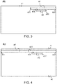
Fig. 3 shows an example of an antenna according to an aspect of the present disclosure. -
Fig. 4 shows an example of an antenna according to an aspect of the present disclosure. -
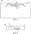
Fig. 5 shows an example of an antenna according to an aspect of the present disclosure. -
Fig. 6 shows an example of an antenna according to an aspect of the present disclosure. -
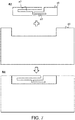
Fig. 7 shows an example of an antenna according to an aspect of the present disclosure. -
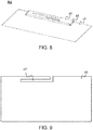
Fig. 8 shows an example of an antenna according to an aspect of the present disclosure. -
Fig. 9 shows an example of an antenna. -
Fig. 10 shows an example of an antenna. -
Fig. 11 shows an example of an antenna. -
Fig. 12 shows an example of characteristics of an antenna. -
Fig. 13 shows an example of characteristics of an antenna according to an aspect of the present disclosure. -
Fig. 14 shows an example of an antenna according to an aspect of the present disclosure. -
Fig. 15 shows an example of an antenna according to an aspect of the present disclosure. -
Fig. 16 shows an example of an antenna according to an aspect of the present disclosure. -
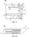
Fig. 17 shows an example of an antenna according to an aspect of the present disclosure. -
Fig. 18 shows an example of an antenna according to an aspect of the present disclosure. -
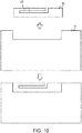
Fig. 19 shows an example of an antenna according to an aspect of the present disclosure. -
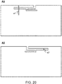
Fig. 20 shows an example of an antenna according to an aspect of the present disclosure (front side and back side). -
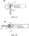
Fig. 21 shows an example of an antenna according to an aspect of the present disclosure. -
Fig. 22 shows an example of an antenna according to an aspect of the present disclosure. -
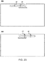
Fig. 23 shows an example of an antenna according to an aspect of the present disclosure (front side and back side). -
Fig. 24 shows an example of an antenna according to an aspect of the present disclosure (front side and back side). -
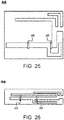
Fig. 25 shows an example of an antenna according to an aspect of the present disclosure. -
Fig. 26 shows an example of an antenna according to an aspect of the present disclosure. -
Fig. 27 shows an example of an antenna according to an aspect of the present disclosure. - All aspects in the present disclosure are merely exemplary and are not intended to exclude other examples from the present disclosure or to limit the technical scope of the invention described in the claims.
- There may be a case where the description may be omitted in part about combinations of aspects in the present disclosure. The omission is intended to simplify the description but not intended to exclude the combinations from the present disclosure nor limit the technical scope of the inventions described in claims. Regardless of whether the omission is made or not, all combinations of the aspects in the present disclosure explicitly, implicitly, or intrinsically included in the present disclosure. In other words, regardless of whether the omission is made or not, all combinations of the aspects in the present disclosure can be derived from the present disclosure directly and clearly.
- For example, as shown in each of
Figs. 1-8 , an antenna according to an aspect of the present disclosure may be an antenna A1 which is provided with a conductive plate a1, wherein: the conductive plate a1 is provided with a slot a2 and a branch slot a3; and the branch slot a3 has one end a31 coupled to the slot a2 and another end a32 extending along the slot a2, in a direction toward an antinode of an electric field at the lowest-order resonance frequency of the antenna A1 when viewed from the end a31, and shorted in the conductive plate a1. - For example, as shown in each of
Figs. 1, 2 ,3 ,6 ,7 and8 , an antenna according to an aspect of the present disclosure may be an antenna A1 which is provided with a conductive plate a1, wherein: the conductive plate a1 is provided with a slot a2 and a branch slot a3; the slot a2 has one end a21 shorted in the conductive plate a1 and another end a22 opened at an edge of the conductive plate; and the branch slot a3 has one end a31 coupled to the slot a2 and another end a32 extending along the slot a2, in a direction toward the other end a22 of the slot a2 when viewed from the end a31 of the branch slot a3, and shorted in the conductive plate a1. - For example, as shown in
Fig. 4 , an antenna according to an aspect of the present disclosure may be an antenna A1 which is provided with a conductive plate a1, wherein: the conductive plate a1 is provided with a slot a2 and a branch slot a3; the slot a2 has both ends a21 and a22 opened at edges of the conductive plate a1; and the branch slot a3 has one end a31 coupled to the slot a2 and another end a32 extending along the slot a2, in a direction toward nearer one of the openings of the slot a2 when viewed from the one end a31 (in a direction toward the end a22), and shorted in the conductive plate a1. - For example, as shown in
Fig. 5 , an antenna according to an aspect of the present disclosure may be an antenna A1 which is provided with a conductive plate a1, wherein: the conductive plate a1 is provided with a slot a2 and a branch slot a3; the slot a2 has both ends a21 and a22 shorted, respectively, in the conductive plate a1; and the branch slot a3 has one end a31 coupled to the slot a2 and another end a32 extending along the slot a2, in a direction toward a middle point a23 in the slot a2 when viewed from the end a31, and shorted in the conductive plate a1. - For example, as shown in
Fig. 6 , the conductive plate a1 may be formed by only a periphery part of the slot a2 and the branch slot a3. - For example, as shown in
Fig. 7 or8 , the conductive plate a1 may formed by coupling a periphery part of the slot a2 and the branch slot a3 to another part. Owing to the coupling, both parts may be formed in practically the same layer or may be formed in different layers as shown inFig. 8 . - The word of "slot" includes a concept of a shape that one of both ends thereof opens at an edge, a concept of a shape that the both ends thereof open at edges and a concept of a shape that the both ends thereof are not opened at the edges.
- The "antinode of an electric field" represents the maximum point of electric field strength, and "a node of an electric field" represents the minimum point of the electric field strength.
- For example, in the aspect according to each of
Figs. 1, 2 and3 , at the lowest-order (first) resonance frequency, the antinode of the electric field occurs in the end a22, and the node of the electric field occurs in the end a21. - Accordingly, in the aspect according to each of
Figs. 1, 2 and3 , the "direction toward an antinode of an electric field at the lowest-order resonance frequency of the antenna A1" is the "direction toward the end a22". - For example, in the aspect according to
Fig. 4 , at the lowest-order (first) resonance frequency, the antinode of the electric field occur at each of the end a21 and the end a22, and the node of the electric field occurs at the middle point a23. - Accordingly, in the aspect according to
Fig. 4 , the "direction toward an antinode of an electric field at the lowest-order resonance frequency of the antenna A1" is the "direction toward nearer one of the openings of the slot a2 when viewed from the end a31 (in a direction toward the end a22)". - For example, in the aspect according to
Fig. 5 , at the lowest-order (first) resonance frequency, the antinode of the electric field occurs at the middle point a23, and the node of the electric field occurs at each of the one end a21 and the other end a22. Accordingly, in the aspect according toFig. 5 , the "direction toward an antinode of an electric field at the lowest-order resonance frequency of the antenna A1" is the "direction toward the middle point a23". - For example, each of
Figs. 9 ,10 and11 shows an antenna having no branch slot a3. - For example, in each of
Figs. 10 and11 , a conductive plate a1 is formed by coupling a periphery part of a slot a2 to a part other than the periphery part, wherein by the coupling, both parts may be formed in practically the same layer or may be formed in different layers as shown inFig. 11 . - For example, in the antenna of the aspect having no branch slot a3 as shown in each of
Figs. 9 ,10 and11 , impedance is matched at each of a first resonance frequency and a third resonance frequency but is not matched at a second resonance frequency as shown inFig. 12 . - In contrast, in an antenna according to an aspect of the disclosure, impedance is matched at each of a first resonance frequency, a second resonance frequency and a third resonance frequency as shown in
Fig. 13 , for example. - In other words, according to an aspect of the present disclosure, a small antenna which can achieve impedance matching at a plurality of resonance frequencies can be provided, for example.
- For example, as shown in each of
Figs. 14-17 , an antenna according to an aspect of the present disclosure (e.g. the antenna A1 or a modified example thereof) may be an antenna A2, wherein: a conductive plate a1 is provided with a passive coupling slot a4; and the passive coupling slot a4 has one end a41 coupled to a slot a2 in proximity of an opening (in proximity of an end a22) and another end a42 shorted in the conductive plate a1. - For example, only one passive coupling slot a4 may be provided as shown in
Fig. 14 . - For example, a plurality of passive coupling slots a4 may be provided as shown in each of
Figs. 15-17 . - For example, the passive coupling slot a4 contributes to radiation by indirectly feeding from feeding to the slot a2.
- Thus, according to an aspect of the disclosure, a small antenna which operates at a wider frequency band can be provided, for example.
- For example, an antenna according to an aspect of the present disclosure (e.g. an antenna A1 or A2, or a modified example thereof) may be an antenna A3, wherein: a conductive plate a1 is attached to an edge of substrate a5 so as to be practically perpendicular to the substrate a5; and an opening of a slot a2 in the conductive plate a1 is on a side, which is practically perpendicular to the substrate a5, of the conductive plate a1.
- For example, the opening of the slot a2 in the conductive plate a1 may be on a side, which is practically parallel to the substrate a5, of the conductive plate a1.
- For example, when the opening of the slot a2 in the conductive plate a1 is on the side practically perpendicular to the substrate a5, there is a case where characteristics of the antenna becomes better.
- Thus, according to an aspect of the present disclosure, for example, a small antenna having better characteristics can be provided.
- For example, as shown in
Fig. 19 , an antenna according to an aspect of the present disclosure (e.g. an antenna A1 or A2, or a modified example thereof) may be an antenna A4, wherein: a conductive plate a1 is formed so as to be practically perpendicular to a reflection plate a6; and an opening of a slot a2 in the conductive plate a1 is on a side, which is practically perpendicular to the reflection plate a6, of the conductive plate a1. - For example, the opening of the slot a2 in the conductive plate a1 may be on a side, which is practically parallel to the reflection plate a6, of the conductive plate a6.
- For example, when the opening of the slot a2 in the conductive plate a1 is at the side practically perpendicular to the reflection plate a6, there is a case where characteristics of the antenna becomes better.
- Thus, according to an aspect of the present disclosure, for example, a small antenna having better characteristics can be provided.
- For example, as shown in each of
Figs. 20-22 , an antenna according to an aspect of the present disclosure (e.g. an antenna A1, A2, A3 or A4, or a modified example thereof) may be an antenna A5, wherein: a region, which is adjacent to a first long side of a slot a2, of a conductive plate a1 is fed; and a region, which is adjacent to a second long side of the slot a2, of the conductive plate a1 is grounded. - Any one of long sides of the slot a2 may be the first long side or the second long side.
- For example, as shown in
Fig.20 , the antenna A5 may be fed by means of a feeding line a7 electrically connected to the region, which is adjacent to the first long side of the slot a2, of the conductive plate a1. - The words of "electrically connected" include both of a concept of electrical connection that conductors are directly connected to each other and a concept of electric connection of wireless feeding, such as EM feeding.
- For example, the feeding line a7 may be provided in a layer other than the conductive plate a1 and may be connected to the conductive plate a1 though vias, etc.
- For example, the feeding line a7 may be provided in a layer identical to a layer in which the conductive plate a1 is and may form a coplanar line by further extending along a clearance provided in the conductive plate a1.
- For example, the feeding line a7 may be formed with an electrical wire such as a transmission line or by a metal plate.
- For example, the conductive plate a1 and a metal plate part of the feeding line a7 may be formed by cutting out from a conductive plate using laser, etc.
- For example, the feeding line a7 may be formed with a coaxial cable as shown in each of
Figs. 21 and 22 . - For example, a core wire a71 of the coaxial cable may be electrically connected to a region, which is adjacent to a first long side of a slot a2, of a conductive plate a1 by means of soldering, etc. as shown in
Fig. 21 , and a connecting aspect may use an auxiliary conductor and a via as shown inFig. 22 , for example. - For example, an outer conductor a72 of the coaxial cable may be electrically connected to the conductive plate a1 by means of soldering, etc. so that a region, which is adjacent to a second long side of the slot a2, of the conductive plate a1 as shown in
Fig. 21 , and a connecting aspect may use an auxiliary conductor and vias as shown inFig. 22 , for example. - For example, as shown in each of
Figs. 23-26 , an antenna according to an aspect of the present disclosure (e.g. an antenna A1, A2, A3, A4 or A5, or a modified example thereof) may be an antenna A6 which is provided with stubs a8 formed in a layer different from a layer including the conductive plate a1 so as to extend over a slot a2, wherein each of the stubs a8 has one end connected to a region, which is adjacent to a long side of a slot a2, of the conductive plate a1. - For example, the stub a8 may have another end which is not connected to the conductive plate a1.
- For example, the stub a8 may be connected to the conductive plate a1 through a via, etc.
- For example, one or two or more stubs a8 may be provided.
- For example, the stub a8 may be made of a metal plate.
- For example, the conductive plate a1 and the stubs a8 may be formed by cutting out from a conductive plate using laser etc.
- For example, the feeding line a7 and the stubs a8 may be formed in the same layer or different layers.
- Thus, according to an aspect of the present disclosure, for example, inductance can be reduced for a resonance frequency according to capacitance increased by the stubs a8.
- In other words, according to an aspect of the present disclosure, a small antenna which can achieve impedance matching at a plurality of resonance frequencies can be provided, for example.
- For example, as shown in
Fig. 27 , an antenna according to an aspect of the disclosure (e.g. an antenna A1, A2, A3, A4 or A5, or a modified example thereof) may be an antenna A7 which is provided with stabs a9 formed inside a slot a2 in the same layer as a layer including a conductive plate a1. - For example, another end of each of the stubs a9 may not be connected to a conductive plate a1.
- For example, the other end of the stub a9 may be connected to the conductive plate a1.
- For example, one or two or more stubs a9 may be provided.
- For example, the stub a9 may have any shape, such as a straight line, a curved line, a bend line, etc.
- For example, the stub a9 may has any shape, such as an L-shape, a T-shape, a meander shape, etc.
- The words of meander shape include a concept represented by words of a zigzag shape, a comb tooth shape, a shape based on an interdigital structure, etc.
- For example, the meander shape is formed by combining straight lines, curved lines, bent lines, etc.
- For example, the stub a9 is made of a metal plate.
- For example, the conductive plate a1 and the stabs a9 may be formed by cutting out from a conductive plate using laser etc.
- Thus, according to an aspect of the present disclosure, for example, inductance can be reduced for a resonance frequency according to capacitance increased by the stubs a9.
- In other words, according to an aspect of the present disclosure, a small antenna which can achieve impedance matching at a plurality of resonance frequencies can be provided, for example.
- For example, a communication device according to an aspect of the present disclosure may be provided with an antenna according to an aspect of the present disclosure (an antenna A1, A2, A3, A4, A5, A6 or A7, or a modified example thereof).
- Thus, according to an aspect of the present disclosure, for example, a communication device provided with a small antenna which can achieve impedance matching at a plurality of resonance frequencies can be provided.
- Although the specific explanation about the present invention is made above referring to the embodiments, the present invention is not limited thereto. In the structure and details of the present invention, various modifications which can be understood by those skilled in the art are susceptible within the scope of the invention.
- The present invention is based on
Japanese Patent Application No. 2019-2527 filed on January 10, 2019 -
- A1, A 2, A 3, A 4, A 5, A 6, A7: antenna
- a1: conductive plate
- a2: slot
- a3: branch slot
- a4: passive coupling slot
- a5: substrate
- a6: reflection plate
- a7: feeding line
- a71: core wire
- a72: outer conductor
- a73: solder
- a8, a9: stub
Claims (11)
- An antenna comprising a conductive plate, wherein:the antenna comprises the conductive plate;the conductive plate comprises a slot and a branch slot;one end of the branch slot is coupled to the slot; andanother end of the branch slot extends along the slot, in a direction toward an antinode of an electric field at a minimum order resonance frequency of the antenna when viewed from the one end, and is shorted in the conductive plate.
- An antenna comprising a conductive plate, wherein:the conductive plate comprises a slot and a branch slot;one end of the slot is shorted in the conductive plate;another end of the slot forms an opening at an edge of the conductive plate;one end of the branch slot is coupled to the slot; andanother end of the branch slot extends along the slot, in a direction toward the other end of the slot when viewed from the one end of the branch slot, and is shorted in the conductive plate.
- An antenna comprising a conductive plate, wherein:the conductive plate comprises a slot and a branch slot;both ends of the slot form openings at edges of the conductive plate;one end of the branch slot is coupled to the slot; andanother end of the branch slot extends along the slot, in a direction toward nearer one of the openings of the slot when viewed from the one end, and is shorted in the conductive plate.
- The antenna as recited in any one of claims 1 to 3, wherein:the conductive plate comprises a passive coupling slot;one end of the passive coupling slot is coupled to the slot in proximity of an opening of the slot; andanother end of the passive coupling slot is shorted in the conductive plate.
- The antenna as recited in any one of claims 1 to 4, wherein:the conductive plate is attached to an edge of a substrate so as to be practically perpendicular to the substrate; andan opening of the slot in the conductive plate is on a side of the conductive plate, the side being practically perpendicular to the substrate.
- The antenna as recited in any one of claims 1 to 4, wherein:the conductive plate is formed so as to be practically perpendicular to a reflection plate; andan opening of the slot in the conductive plate is on a side of the conductive plate, the side being practically perpendicular to the reflection plate.
- An antenna comprises a conductive plate, wherein:the conductive plate comprises a slot and a branch slot;both ends of the slot are shorted in the conductive plate;one end of the branch slot is coupled to the slot; andanother end of the branch slot extends along the slot, in a direction toward a middle point of the slot when viewed from the one end, and is shorted in the conductive plate.
- The antenna as recited in any one of claims 1 to 7, wherein:a region of the conductive plate is fed, the region being adjacent to a first long side of the slot; anda region of the conductive plate is grounded, the region being adjacent to a second long side of the slot is grounded.
- The antenna as recited in any one of claims 1 to 8, wherein:the antenna comprises a stub which is formed in a layer different from a layer including the conductive plate so as to extend over the slot; andone end of the stub is connected to a region of the conductive plate, the region being adjacent to a long side of the slot.
- The antenna as recited in any one of claims 1 to 8, wherein:the antenna comprises a stub which is formed inside the slot in a layer identical with a layer including the conductive plate;one end of the stub is connected to a region of the conductive plate, the region being adjacent to a long side of the slot.
- A communication device comprising the antenna as recited in any one of claims 1 to 10.
Applications Claiming Priority (2)
| Application Number | Priority Date | Filing Date | Title |
|---|---|---|---|
| JP2019002527 | 2019-01-10 | ||
| PCT/JP2019/047901 WO2020144994A1 (en) | 2019-01-10 | 2019-12-06 | Antenna and communication device |
Publications (2)
| Publication Number | Publication Date |
|---|---|
| EP3876347A1 true EP3876347A1 (en) | 2021-09-08 |
| EP3876347A4 EP3876347A4 (en) | 2021-12-29 |
Family
ID=71520760
Family Applications (1)
| Application Number | Title | Priority Date | Filing Date |
|---|---|---|---|
| EP19909525.8A Withdrawn EP3876347A4 (en) | 2019-01-10 | 2019-12-06 | Antenna and communication device |
Country Status (7)
| Country | Link |
|---|---|
| US (1) | US20220029296A1 (en) |
| EP (1) | EP3876347A4 (en) |
| JP (1) | JPWO2020144994A1 (en) |
| KR (1) | KR20210082245A (en) |
| CN (1) | CN113196570A (en) |
| TW (1) | TW202038507A (en) |
| WO (1) | WO2020144994A1 (en) |
Families Citing this family (6)
| Publication number | Priority date | Publication date | Assignee | Title |
|---|---|---|---|---|
| CN112993579B (en) * | 2021-02-08 | 2023-07-25 | Oppo广东移动通信有限公司 | Antenna devices and electronic equipment |
| JP7608267B2 (en) * | 2021-05-19 | 2025-01-06 | 日本航空電子工業株式会社 | Multi-band Antennas |
| WO2022264455A1 (en) * | 2021-06-14 | 2022-12-22 | パナソニックIpマネジメント株式会社 | Antenna device, and method for manufacturing antenna device |
| JP7704037B2 (en) * | 2022-01-14 | 2025-07-08 | ソニーグループ株式会社 | Antenna device, electronic device |
| TWI872611B (en) * | 2022-09-22 | 2025-02-11 | 仁寶電腦工業股份有限公司 | Electronic device and antenna module |
| US20260149184A1 (en) * | 2024-11-22 | 2026-05-28 | Intel Corporation | Printed high-isolation multi-feed antenna |
Family Cites Families (31)
| Publication number | Priority date | Publication date | Assignee | Title |
|---|---|---|---|---|
| US4686536A (en) * | 1985-08-15 | 1987-08-11 | Canadian Marconi Company | Crossed-drooping dipole antenna |
| US6343208B1 (en) * | 1998-12-16 | 2002-01-29 | Telefonaktiebolaget Lm Ericsson (Publ) | Printed multi-band patch antenna |
| TW490885B (en) * | 2001-05-25 | 2002-06-11 | Chi Mei Comm Systems Inc | Broadband dual-band antenna |
| TW507946U (en) * | 2001-11-09 | 2002-10-21 | Hon Hai Prec Ind Co Ltd | Dual band slotted antenna |
| US6621455B2 (en) * | 2001-12-18 | 2003-09-16 | Nokia Corp. | Multiband antenna |
| US7002519B2 (en) * | 2001-12-18 | 2006-02-21 | Nokia Corporation | Antenna |
| US6646610B2 (en) * | 2001-12-21 | 2003-11-11 | Nokia Corporation | Antenna |
| US20040257283A1 (en) * | 2003-06-19 | 2004-12-23 | International Business Machines Corporation | Antennas integrated with metallic display covers of computing devices |
| US7932863B2 (en) * | 2004-12-30 | 2011-04-26 | Fractus, S.A. | Shaped ground plane for radio apparatus |
| JP4418375B2 (en) * | 2005-01-25 | 2010-02-17 | アルプス電気株式会社 | Antenna device |
| CN101828304A (en) * | 2007-10-19 | 2010-09-08 | Nxp股份有限公司 | Dual band slot antenna |
| TWI351786B (en) * | 2007-11-22 | 2011-11-01 | Arcadyan Technology Corp | Dual band antenna |
| US8259021B2 (en) * | 2008-12-22 | 2012-09-04 | Industrial Technology Research Institute | Electromagnetic radiation apparatus and method for forming the same |
| TWI380511B (en) * | 2008-12-26 | 2012-12-21 | Arcadyan Technology Corp | Multi-band antenna |
| JP5699820B2 (en) * | 2010-09-16 | 2015-04-15 | 日本電気株式会社 | Antenna device |
| CN102544716A (en) * | 2010-12-30 | 2012-07-04 | 希姆通信息技术(上海)有限公司 | Substrate with multi-frequency slot antenna |
| CN103348536B (en) * | 2011-02-09 | 2015-06-17 | 日本电气株式会社 | Slot antenna |
| US20120262355A1 (en) * | 2011-04-18 | 2012-10-18 | Ziming He | High gain low profile multi-band antenna for wireless communications |
| WO2013124897A1 (en) * | 2012-02-23 | 2013-08-29 | 日本電気株式会社 | Antenna apparatus |
| TWI581499B (en) * | 2012-03-15 | 2017-05-01 | 富智康(香港)有限公司 | Antenna assembly |
| US9318793B2 (en) * | 2012-05-02 | 2016-04-19 | Apple Inc. | Corner bracket slot antennas |
| FR2990591A1 (en) * | 2012-05-14 | 2013-11-15 | Thomson Licensing | METHOD OF MAKING A LINE-SLIT ON A MULTILAYER SUBSTRATE AND MULTI-LAYER PRINTED CIRCUIT COMPRISING AT LEAST ONE LINE-SLIT REALIZED ACCORDING TO SAID METHOD AND USED AS AN INSULATED SLOT OR ANTENNA |
| CN103531905A (en) * | 2012-07-06 | 2014-01-22 | 宏碁股份有限公司 | Electronic device |
| US9099789B1 (en) * | 2012-09-05 | 2015-08-04 | Amazon Technologies, Inc. | Dual-band inverted slot antenna |
| US9099790B2 (en) * | 2012-12-27 | 2015-08-04 | Htc Corporation | Mobile device and antenna structure therein |
| US20150002351A1 (en) * | 2013-06-28 | 2015-01-01 | Research In Motion Limited | Slot antenna with a combined bandpass/bandstop filter network |
| TWI568076B (en) * | 2014-03-17 | 2017-01-21 | 廣達電腦股份有限公司 | Antenna structure |
| WO2015151139A1 (en) * | 2014-03-31 | 2015-10-08 | 日本電気株式会社 | Antenna, antenna array, and wireless communication device |
| KR102508922B1 (en) * | 2016-11-07 | 2023-03-13 | 삼성전자주식회사 | Electronic device comprising antenna |
| JP2018170589A (en) * | 2017-03-29 | 2018-11-01 | 富士通株式会社 | ANTENNA DEVICE AND ELECTRONIC DEVICE |
| JP2019002527A (en) | 2017-06-19 | 2019-01-10 | 日産自動車株式会社 | Oil suction device |
-
2019
- 2019-12-06 KR KR1020217016503A patent/KR20210082245A/en not_active Abandoned
- 2019-12-06 US US17/298,288 patent/US20220029296A1/en not_active Abandoned
- 2019-12-06 CN CN201980079048.7A patent/CN113196570A/en active Pending
- 2019-12-06 JP JP2020565632A patent/JPWO2020144994A1/ja active Pending
- 2019-12-06 WO PCT/JP2019/047901 patent/WO2020144994A1/en not_active Ceased
- 2019-12-06 EP EP19909525.8A patent/EP3876347A4/en not_active Withdrawn
-
2020
- 2020-01-09 TW TW109100673A patent/TW202038507A/en unknown
Also Published As
| Publication number | Publication date |
|---|---|
| CN113196570A (en) | 2021-07-30 |
| WO2020144994A1 (en) | 2020-07-16 |
| TW202038507A (en) | 2020-10-16 |
| US20220029296A1 (en) | 2022-01-27 |
| JPWO2020144994A1 (en) | 2020-07-16 |
| KR20210082245A (en) | 2021-07-02 |
| EP3876347A4 (en) | 2021-12-29 |
Similar Documents
| Publication | Publication Date | Title |
|---|---|---|
| US20220029296A1 (en) | Antenna and communication device | |
| CN110574234B (en) | Antenna and MIMO antenna | |
| US9825366B2 (en) | Printed circuit board antenna and printed circuit board | |
| US6700543B2 (en) | Antenna element with conductors formed on outer surfaces of device substrate | |
| CN1720638A (en) | means for connecting additional antennas to radio equipment | |
| AU4892800A (en) | An antenna with stacked resonant structures and a multi- frequency radiocommunications system including it | |
| US11240909B2 (en) | Antenna device | |
| CN101207237B (en) | Improvement to radiating slot planar antennas | |
| CN101099267B (en) | Slot antenna | |
| EP3826110A1 (en) | Antenna and communication device | |
| EP3790114A1 (en) | Split-ring resonator and substrate | |
| EP2569823B1 (en) | Antenna having planar conducting elements | |
| JPH10261914A (en) | Antenna device | |
| US10201076B2 (en) | Coupler for proximity wireless communication | |
| EP4092827B1 (en) | Multiband antenna | |
| CN110336130A (en) | A kind of dipole filter antenna and electronic equipment | |
| US7671695B2 (en) | Parallel coupled CPW line filter | |
| CN101740866A (en) | Multi-frequency antenna for wireless communication device | |
| US11424536B2 (en) | Multiband compatible antenna and radio communication device | |
| US9722307B2 (en) | Terminal antenna structure and terminal | |
| CN110808460A (en) | Dual-band antenna and aircraft | |
| CN206650166U (en) | Multifrequency antenna | |
| US11233331B2 (en) | Antenna device | |
| EP3065216A1 (en) | Monopole antenna | |
| CN112821037B (en) | Multi-frequency antenna |
Legal Events
| Date | Code | Title | Description |
|---|---|---|---|
| STAA | Information on the status of an ep patent application or granted ep patent |
Free format text: STATUS: THE INTERNATIONAL PUBLICATION HAS BEEN MADE |
|
| PUAI | Public reference made under article 153(3) epc to a published international application that has entered the european phase |
Free format text: ORIGINAL CODE: 0009012 |
|
| STAA | Information on the status of an ep patent application or granted ep patent |
Free format text: STATUS: REQUEST FOR EXAMINATION WAS MADE |
|
| 17P | Request for examination filed |
Effective date: 20210531 |
|
| AK | Designated contracting states |
Kind code of ref document: A1 Designated state(s): AL AT BE BG CH CY CZ DE DK EE ES FI FR GB GR HR HU IE IS IT LI LT LU LV MC MK MT NL NO PL PT RO RS SE SI SK SM TR |
|
| REG | Reference to a national code |
Ref country code: DE Ref legal event code: R079 Free format text: PREVIOUS MAIN CLASS: H01Q0005357000 Ipc: H01Q0013100000 |
|
| A4 | Supplementary search report drawn up and despatched |
Effective date: 20211126 |
|
| RIC1 | Information provided on ipc code assigned before grant |
Ipc: H01Q 1/24 20060101ALI20211122BHEP Ipc: H01Q 5/371 20150101ALI20211122BHEP Ipc: H01Q 13/10 20060101AFI20211122BHEP |
|
| DAV | Request for validation of the european patent (deleted) | ||
| DAX | Request for extension of the european patent (deleted) | ||
| STAA | Information on the status of an ep patent application or granted ep patent |
Free format text: STATUS: EXAMINATION IS IN PROGRESS |
|
| 17Q | First examination report despatched |
Effective date: 20220803 |
|
| STAA | Information on the status of an ep patent application or granted ep patent |
Free format text: STATUS: THE APPLICATION IS DEEMED TO BE WITHDRAWN |
|
| 18D | Application deemed to be withdrawn |
Effective date: 20230620 |