EP3876297A1 - Display panel and preparation method therefor, and display device - Google Patents
Display panel and preparation method therefor, and display device Download PDFInfo
- Publication number
- EP3876297A1 EP3876297A1 EP19931277.8A EP19931277A EP3876297A1 EP 3876297 A1 EP3876297 A1 EP 3876297A1 EP 19931277 A EP19931277 A EP 19931277A EP 3876297 A1 EP3876297 A1 EP 3876297A1
- Authority
- EP
- European Patent Office
- Prior art keywords
- conductive layer
- layer
- transparent conductive
- light
- substrate
- Prior art date
- Legal status (The legal status is an assumption and is not a legal conclusion. Google has not performed a legal analysis and makes no representation as to the accuracy of the status listed.)
- Pending
Links
Images




Classifications
-
- H—ELECTRICITY
- H10—SEMICONDUCTOR DEVICES; ELECTRIC SOLID-STATE DEVICES NOT OTHERWISE PROVIDED FOR
- H10K—ORGANIC ELECTRIC SOLID-STATE DEVICES
- H10K59/00—Integrated devices, or assemblies of multiple devices, comprising at least one organic light-emitting element covered by group H10K50/00
- H10K59/10—OLED displays
- H10K59/12—Active-matrix OLED [AMOLED] displays
- H10K59/131—Interconnections, e.g. wiring lines or terminals
-
- H—ELECTRICITY
- H10—SEMICONDUCTOR DEVICES; ELECTRIC SOLID-STATE DEVICES NOT OTHERWISE PROVIDED FOR
- H10K—ORGANIC ELECTRIC SOLID-STATE DEVICES
- H10K59/00—Integrated devices, or assemblies of multiple devices, comprising at least one organic light-emitting element covered by group H10K50/00
- H10K59/10—OLED displays
- H10K59/12—Active-matrix OLED [AMOLED] displays
- H10K59/122—Pixel-defining structures or layers, e.g. banks
-
- H—ELECTRICITY
- H10—SEMICONDUCTOR DEVICES; ELECTRIC SOLID-STATE DEVICES NOT OTHERWISE PROVIDED FOR
- H10K—ORGANIC ELECTRIC SOLID-STATE DEVICES
- H10K50/00—Organic light-emitting devices
- H10K50/80—Constructional details
- H10K50/805—Electrodes
- H10K50/81—Anodes
- H10K50/818—Reflective anodes, e.g. ITO combined with thick metallic layers
-
- H—ELECTRICITY
- H10—SEMICONDUCTOR DEVICES; ELECTRIC SOLID-STATE DEVICES NOT OTHERWISE PROVIDED FOR
- H10K—ORGANIC ELECTRIC SOLID-STATE DEVICES
- H10K59/00—Integrated devices, or assemblies of multiple devices, comprising at least one organic light-emitting element covered by group H10K50/00
- H10K59/10—OLED displays
- H10K59/12—Active-matrix OLED [AMOLED] displays
- H10K59/1201—Manufacture or treatment
-
- H—ELECTRICITY
- H10—SEMICONDUCTOR DEVICES; ELECTRIC SOLID-STATE DEVICES NOT OTHERWISE PROVIDED FOR
- H10K—ORGANIC ELECTRIC SOLID-STATE DEVICES
- H10K59/00—Integrated devices, or assemblies of multiple devices, comprising at least one organic light-emitting element covered by group H10K50/00
- H10K59/80—Constructional details
- H10K59/805—Electrodes
- H10K59/8051—Anodes
- H10K59/80516—Anodes combined with auxiliary electrodes, e.g. ITO layer combined with metal lines
-
- H—ELECTRICITY
- H10—SEMICONDUCTOR DEVICES; ELECTRIC SOLID-STATE DEVICES NOT OTHERWISE PROVIDED FOR
- H10K—ORGANIC ELECTRIC SOLID-STATE DEVICES
- H10K59/00—Integrated devices, or assemblies of multiple devices, comprising at least one organic light-emitting element covered by group H10K50/00
- H10K59/80—Constructional details
- H10K59/805—Electrodes
- H10K59/8051—Anodes
- H10K59/80518—Reflective anodes, e.g. ITO combined with thick metallic layers
-
- H—ELECTRICITY
- H10—SEMICONDUCTOR DEVICES; ELECTRIC SOLID-STATE DEVICES NOT OTHERWISE PROVIDED FOR
- H10K—ORGANIC ELECTRIC SOLID-STATE DEVICES
- H10K71/00—Manufacture or treatment specially adapted for the organic devices covered by this subclass
- H10K71/621—Providing a shape to conductive layers, e.g. patterning or selective deposition
-
- H—ELECTRICITY
- H10—SEMICONDUCTOR DEVICES; ELECTRIC SOLID-STATE DEVICES NOT OTHERWISE PROVIDED FOR
- H10K—ORGANIC ELECTRIC SOLID-STATE DEVICES
- H10K2102/00—Constructional details relating to the organic devices covered by this subclass
- H10K2102/10—Transparent electrodes, e.g. using graphene
- H10K2102/101—Transparent electrodes, e.g. using graphene comprising transparent conductive oxides [TCO]
- H10K2102/103—Transparent electrodes, e.g. using graphene comprising transparent conductive oxides [TCO] comprising indium oxides, e.g. ITO
-
- H—ELECTRICITY
- H10—SEMICONDUCTOR DEVICES; ELECTRIC SOLID-STATE DEVICES NOT OTHERWISE PROVIDED FOR
- H10K—ORGANIC ELECTRIC SOLID-STATE DEVICES
- H10K2102/00—Constructional details relating to the organic devices covered by this subclass
- H10K2102/301—Details of OLEDs
- H10K2102/351—Thickness
-
- H—ELECTRICITY
- H10—SEMICONDUCTOR DEVICES; ELECTRIC SOLID-STATE DEVICES NOT OTHERWISE PROVIDED FOR
- H10K—ORGANIC ELECTRIC SOLID-STATE DEVICES
- H10K59/00—Integrated devices, or assemblies of multiple devices, comprising at least one organic light-emitting element covered by group H10K50/00
- H10K59/60—OLEDs integrated with inorganic light-sensitive elements, e.g. with inorganic solar cells or inorganic photodiodes
- H10K59/65—OLEDs integrated with inorganic image sensors
Definitions
- the present disclosure relates to the field of organic light-emitting display, in particular to a display panel and a method for producing same, and a display device.
- OLED Organic light emitting diode
- Some embodiments of the present disclosure provide a display panel and a method for producing same, and a display device, which can improve a light transmittance while reducing the possibility of an abnormal light emission.
- an embodiment of the present disclosure provides a display panel, which includes: a substrate; a pixel defining layer disposed on the substrate; and an electrode layer located between the substrate and the pixel defining layer.
- the pixel defining layer is internally provided with a through hole disposed opposite to the electrode layer, and the through hole penetrates through the pixel defining layer and falls on the electrode layer.
- the electrode layer includes a first transparent conductive layer and a light-shielding conductive layer that are arranged in a stack. Along a stacking direction of the electrode layer, an area of an orthographic projection of the first transparent conductive layer on the substrate is larger than an area of an orthographic projection of the light-shielding conductive layer on the substrate.
- An embodiment of the present disclosure further provides a display device, which includes the display panel as described above.
- An embodiment of the present disclosure further provides a method for producing the display panel, which includes the following steps: providing a substrate; forming an electrode layer on the substrate; and forming a pixel defining layer on the electrode layer, where the pixel defining layer is internally provided with a through hole disposed opposite to the electrode layer, and the through hole penetrates through the pixel defining layer and falls on the electrode layer; where forming the electrode layer on the substrate specifically includes forming a first transparent conductive layer and a light-shielding conductive layer on the substrate by stacking, and along a stacking direction of the electrode layer, an area of an orthographic projection of the first transparent conductive layer on the substrate is larger than an area of an orthographic projection of the light-shielding conductive layer on the substrate.
- An OLED display device has a problem that after reducing an area of an opaque electrode, it is easy to cause a display panel to emit light abnormally.
- the reason for this problem is that the OLED display device in the existing technology is usually provided with a through hole on a pixel defining layer.
- the through hole in the existing technology needs to fall on the opaque electrode.
- the through hole may not completely fall on the electrode, and the problem of abnormal display may occur at this time.
- An embodiment of the present disclosure relates to a display panel, as shown in FIG. 1 , including: a substrate 10, a pixel defining layer 20 disposed on the substrate 10, and an electrode layer 30 located between the substrate 10 and the pixel defining layer 20.
- the pixel defining layer 20 includes a through hole 21 disposed opposite to the electrode layer 30, and the through hole 21 penetrates through the pixel defining layer 20 and falls on the electrode layer 30.
- the electrode layer 30 includes a first transparent conductive layer 31 and a light-shielding conductive layer 32 that are arranged in a stack. Along a stacking direction of the electrode layer 30, an area of an orthographic projection of the first transparent conductive layer 31 on the substrate is larger than an area of an orthographic projection of the light-shielding conductive layer 32 on the substrate.
- the electrode layer 30 is formed by stacking the first transparent conductive layer 31 and the light-shielding conductive layer 32.
- a light transmittance of the first conductive layer 31 is greater than a light transmittance of the light-shielding layer 32, and along the stacking direction of the electrode layer 30, the area of the orthographic projection of the first transparent conductive layer 31 on the substrate is larger than the area of the orthographic projection of the light-shielding conductive layer 32 on the substrate. Therefore, under the condition of having the same light transmittance (that is, an area of an opaque part is the same) as in the existing technology, the electrode layer 30 in the embodiment of the present disclosure has a larger overall area along the stacking direction of the electrode layer 30.
- the electrode layer 30 with a larger area makes the through hole 21 less likely to fall outside the electrode layer 30 when it is arranged in cooperation with the electrode layer 30, thus reducing the possibility of abnormal light emission in the display panel.
- the orthographic projection of the light-shielding conductive layer 32 on the substrate 10 is located inside the orthographic projection of the first transparent conductive layer 31 on the substrate 10. That is, an area where the light-shielding conductive layer 32 is attached with the first transparent conductive layer 31 is at least the area of the orthographic projection of the light-shielding conductive layer 32 on the substrate 10, so that a contact area between the first transparent conductive layer 31 and the light-shielding conductive layer 32 is large, and the first transparent conductive layer 31 may better protect the light-shielding conductive layer 32.
- the orthographic projection of the light-shielding conductive layer 32 on the substrate 10 is located inside the orthographic projection of the first transparent conductive layer 31 on the substrate 10, which is only a specific example of an arrangement state of the first transparent conductive layer 31 and the light-shielding conductive layer 32 in this embodiment. As shown in FIG. 3 , along the stacking direction of the electrode layer 30, the orthographic projection of the light-shielding conductive layer 32 on the substrate 10 may also partially overlap with the orthographic projection of the first transparent conductive layer 31 on the substrate 10.
- the orthographic projection of the light-shielding conductive layer 32 on the substrate 10 partially overlaps with the orthographic projection of the first transparent conductive layer 31 on the substrate 10, so that the overall area of the electrode layer 30 is larger than an overall area of the first transparent conductive layer 31, thereby further increasing the overall area of the electrode layer 30 and further reducing the possibility of abnormal light emission.
- a material of the first transparent conductive layer 31 is ITO or IZO, and a material of the light-shielding conductive layer 32 is a metal or a graphite, where the metal may be a silver, a lead, etc.
- the material of the first transparent conductive layer 31 being the ITO or the IZO is only a specific example of the material of the first transparent conductive layer 31 in this embodiment, and does not constitute a limitation.
- the first transparent conductive layer 31 may also be other materials with both transparent and conductive properties, such as ZnO-based TCO, etc., which are not listed here.
- the material of the light-shielding conductive layer 32 being the metal or the graphite is only a specific example of the material of the light-shielding conductive layer 32 in this embodiment and does not constitute a limitation.
- the light-shielding conductive layer 32 may also be other materials with both light-shielding and conductive properties, such as an opaque conductive plastic, etc., which are not listed here, but may be flexibly selected according to actual needs.
- the first transparent conductive layer 31 is sandwiched between the substrate 10 and the light-shielding conductive layer 32.
- the light-shielding conductive layer 32 is located on a surface of the first transparent conductive layer 31 facing the substrate 10. Since the light-shielding conductive layer 32 made of the metal and other materials has a poor bonding with the substrate 10, in this embodiment, the first transparent conductive layer 31 made of the ITO or the IZO material is sandwiched between the substrate 10 and the light-shielding conductive layer 32, which may make the bonding between layers in the display panel firmer and improve the reliability of the display panel.
- the above-described sandwiching the first transparent conductive layer 31 between the substrate 10 and the light-shielding conductive layer 32 is only an example of a positional relationship among the first transparent conductive layer 31, the substrate 10 and the light-shielding conductive layer 32 in this embodiment, and does not constitute a limitation.
- the light-shielding conductive layer 32 may also be sandwiched between the substrate 10 and the first transparent conductive layer 31.
- the light-shielding conductive layer 32 made of the metal or the graphite is sandwiched between the substrate 10 and the first transparent conductive layer 31, so that the first transparent conductive layer 31 may protect the light-shielding conductive layer 32 and prevent the light-shielding conductive layer 32 from being oxidized.
- the through hole 21 falls on the electrode layer 30.
- the possibility of abnormal light emission of the display panel may be completely eliminated.
- an error reserve area is set at an edge of the electrode layer 30 in advance, that is, a part of the electrode layer 30 close to the edge is set as the error reserve area.
- the error reserve area is an area with a distance less than 2 ⁇ m from the edge of the electrode layer 30.
- the above is only a specific example of the error reserve area in this embodiment. In other embodiments of the present disclosure, the error reserve area may also be of other sizes, which may be flexibly set according to actual needs.
- a sidewall of the through hole 21 at least partially falls on the first transparent conductive layer 31.
- the sidewall of the through hole 21 at least partially falling on the first transparent conductive layer 31 is only an example of a specific position in this embodiment, and does not constitute a limitation. In other embodiments of the present disclosure, the sidewall of the through hole 21 may not fall on the first transparent conductive layer 31, but fall on other parts of the electrode layer 30, such as all falling on the light-shielding conductive layer 32, which is not listed here.
- the electrode layer 30 is an anode layer.
- the substrate 10 sequentially includes a underlay 11, a barrier layer 12 located above the underlay 11, a buffer layer 13 located above the barrier layer 12, a channel 14 located above the buffer layer 13, a first gate insulating layer 15 covering the channel 14, a gate 16 disposed above the first gate insulating layer 15 and a source 17 and a drain 18 penetrating through the first gate insulating layer 15, a second gate insulating layer 19 located above the first gate insulating layer 15 and covering the gate 16, an intermediate insulating layer 10a covering the second gate insulating layer 19, a filling layer 10b covering the intermediate insulating layer 10a, a capacitor lower plate 10c located between the first gate insulating layer 15 and the second gate insulating layer 19, and a capacitor upper plate 10d located between the intermediate insulating layer 10a and the second gate insulating layer 19.
- the electrode layer 30 is disposed on the filling layer 10b and electrically connected to the drain 18 through the filling layer 10b.
- a material of the filling layer 10b is a polylactic acid.
- the material of the filling layer 10b being the polylactic acid is only a specific example in this embodiment.
- the filling layer 10b may also be made of other materials, such as a polyethylene, which are not listed here, but may be flexibly set according to actual needs.
- An embodiment of the present disclosure also relates to a display panel, which is substantially the same as the previous embodiments and also includes a substrate 10, a pixel defining layer 20 disposed on the substrate 10, and an electrode layer 30 located between the substrate 10 and the pixel defining layer 20.
- the pixel defining layer 20 includes a through hole 21 disposed opposite to the electrode layer 30, and the through hole 21 penetrates through the pixel defining layer 20 and falls on the electrode layer 30.
- the electrode layer 30 includes a second transparent conductive layer 33 in addition to a first transparent electrode layer 31 and a light-shielding conductive layer 32.
- a material of the second transparent conductive layer 33 is ITO or IZO.
- the material of the second transparent conductive layer 33 being the ITO or the IZO is only a specific example of the material of the second transparent conductive layer 33 in this embodiment, and does not constitute a limitation.
- the second transparent conductive layer 33 may also be other materials with both transparent and conductive properties, such as ZnO-based TCO, which are not listed here.
- the first transparent conductive layer 31 is sandwiched between the light-shielding conductive layer 32 and the substrate 10, and the light-shielding conductive layer 32 is sandwiched between the first transparent conductive layer 31 and the second transparent conductive layer 33.
- the light-shielding conductive layer 32 is located on a surface of the first transparent conductive layer 31 facing the second transparent conductive layer 33, and the light-shielding conductive layer 32 is located on a surface of the second transparent conductive layer 33 facing the first transparent conductive layer 31.
- the display panel provided by the present embodiment is further provided with the electrode layer 30 including the second transparent conductive layer 33 and the light-shielding conductive layer 32 sandwiched between the first transparent conductive layer 31 and the second transparent conductive layer 33, which may effectively increase a firmness of the combination between various components and improve the reliability of the display panel; and may also protect the light-shielding conductive layer 32 and prevent the light-shielding conductive layer 32 from being oxidized.
- a sidewall of the through hole 21 at least partially falls on the first transparent conductive layer 31.
- the sidewall of the through hole 21 at least partially falling on the first transparent conductive layer 31 is only an example of a specific position in this embodiment, and does not constitute a limitation.
- the sidewall of the through hole 21 may not fall on the first transparent conductive layer 31, but fall on other parts of the electrode layer 30, such as all falling on the second transparent conductive layer 33 or all falling on the light-shielding conductive layer; or the sidewall of the through hole 21 may also at least partially fall on the light-shielding conductive layer 32; or the sidewall of the through hole 21 may also at least partially fall on the second transparent conductive layer 33, which are not listed here.
- An area of the second transparent conductive layer 33 is equal to an area of the light-shielding conductive layer 32 along a stacking direction of the electrode layer 30.
- the area of the second transparent conductive layer 33 being equal to the area of the light-shielding conductive layer 32 is only a specific application example in this embodiment, which does not constitute a limitation.
- the area of the second transparent conductive layer 33 may be larger than the area of the light-shielding conductive layer 32, even if the second transparent conductive layer 33 completely covers an upper surface and a side surface of the light-shielding conductive layer 32.
- the area of the second transparent conductive layer 33 may be smaller than the area of light-shielding conductive layer 32, that is, part of the upper surface of the light-shielding conductive layer 32 is exposed.
- a thickness of the first transparent conductive layer 31 and a thickness of the second transparent conductive layer 33 are both greater than or equal to 8 nm and less than or equal to 15 nm.
- the thickness of the first transparent conductive layer 31 and the thicknesses of the second transparent conductive layer 33 may be the same or different.
- the thickness of the first transparent conductive layer 31 and the thicknesses of the second transparent conductive layer 33 are both 10 nm.
- a thickness of the light-shielding conductive layer 32 is greater than or equal to 80 nm and less than or equal to 120 nm.
- the thickness of the light-shielding conductive layer 32 is 100 nm.
- An embodiment of the present disclosure relates to a display device, which includes the display panel provided by other embodiments of the present disclosure.
- the display device provided by the embodiment of the present disclosure includes the display panel provided by other embodiments of the present disclosure. Therefore, the display device provided by this embodiment has all the technical effects of the display panel provided by other embodiments of the present disclosure, which is not repeated here.
- An embodiment of the present disclosure relates to a method for producing a display panel, as shown in FIG. 7 , which includes the following steps.
- an electrode layer is formed on the substrate.
- the electrode layer includes a first transparent conductive layer and a light-shielding conductive layer that are formed by stacking.
- the first transparent conductive layer and the light-shielding conductive layer are formed on the substrate by stacking to serve as the electrode layer.
- a projection area of the first transparent conductive layer is larger than a projection area of the light-shielding conductive layer in a stacking direction of the electrode layer.
- a pixel defining layer is formed on the electrode layer.
- the pixel defining layer is internally provided with a through hole disposed opposite to the electrode layer, and the through hole penetrates through the pixel defining layer and falls on the electrode layer.
- the through hole falls on the electrode layer, that is, side walls of the through hole all fall on the electrode layer.
- a preset position of the through hole is a region away from an edge of the electrode layer by a preset distance.
- the preset distance is less than 3 ⁇ m.
- the preset distance is 2 ⁇ m.
- the preset distance being 2 ⁇ m is only a specific example in this embodiment, and does not constitute a limitation. In other embodiments of the present disclosure, the preset distance may also be other values, which are not listed here, but may be flexibly set according to actual needs.
- This embodiment is an embodiment of the method for producing the display panel corresponding to the embodiments mentioned above, and this embodiment may be implemented in cooperation with the embodiments mentioned above.
- the relevant technical details mentioned in the above-mentioned embodiments are still valid in this embodiment, and in order to reduce repetition, they will not be repeated here.
- the relevant technical details mentioned in this embodiment may also be applied in the above-mentioned embodiments.
- the display panel prepared by the method for producing the display panel provided by the embodiment of the present disclosure increases an anode area, where an increased anode area is a transparent ITO or IZO film which has almost no influence on a light transmittance of a screen body, and fundamentally prevents an effect that the pixel defining layer is unable to completely wrap the anode, thereby greatly increasing a process allowance of wrapping the anode with the pixel defining layer, effectively reducing a requirement on an alignment accuracy of the pixel defining layer and the anode, and simplifying the process steps.
- An embodiment of the present disclosure relates to a method for producing a display panel, as shown in FIG. 8 , which includes the following steps.
- an electrode layer is formed on the substrate.
- the electrode layer includes a first transparent conductive layer, a light-shielding conductive layer, and a second transparent conductive layer that are formed by stacking.
- the electrode layer is formed on the substrate, which specifically includes the following steps.
- a first transparent conductive layer 31 is formed on the substrate, a light-shielding conductive layer 32 covering the first transparent conductive layer 31 is formed on the first transparent conductive layer 31, a second transparent conductive layer 33 covering the light-shielding conductive layer 32 is formed on the second transparent conductive layer 33, and a photoresist layer 40 covering the second transparent conductive layer 33 is formed on the second transparent conductive layer 33.
- the photoresist layer is patterned.
- a first photoresist region 331, a second photoresist region 332 and a photoresist-free region 333 are formed on the second transparent conductive layer 33 in parallel.
- the photoresist layer is patterned through an exposure and development process using a semi light-transmissive mask 50.
- the semi light-transmissive mask 50 includes a fully light-transmissive region 51, a semi light-transmissive region 52 and an optically opaque region 53.
- a transparency of the semi light-transmissive region 52 is greater than a transparency of the optically opaque region 53 but less than a transparency of the fully light-transmissive region 51.
- the first photoresist region 331 is formed below the optically opaque region 53
- the second photoresist region 332 is formed below the semi light-transmissive region 52
- the photoresist-free region 333 is formed below fully light-transmissive region 51.
- a thickness of a photoresist layer on a surface of the second photoresist region 332 is smaller than a thickness of a photoresist layer on a surface of the first photoresist region 331.
- the first transparent conductive layer 31, the light-shielding conductive layer 32 and the second transparent conductive layer 33 in the photoresist-free region are removed.
- the first transparent conductive layer 31 and the second transparent conductive layer 33 are etched using an oxalic acid etching solution.
- the light-shielding conductive layer 32 is etched using a mixed acid etching solution of HNO3, CH3COOH, and H3PO4.
- the photoresist layer on the surface of the second photoresist region 332 is removed.
- a reaction is carried out by using SF6+O2 gas through a dry ashing process to remove the photoresist layer on the surface of the first photoresist region 332.
- a photoresist layer 40 on the surface of the second photoresist region 333 also reacts and decreases, resulting in a decrease in the thickness of the photoresist layer 40 on the surface of the second photoresist region 333.
- the light-shielding conductive layer 32 and the second transparent conductive layer 33 in the second photoresist region are removed, and the photoresist layer on the surface of the first photoresist region 331 is removed.
- the second transparent conductive layer and the light-shielding conductive layer which are not shielded by the photoresist layer are removed by a two-step wet etching.
- the second transparent conductive layer 33 is etched using the oxalic acid etching solution.
- the light-shielding conductive layer 32 is etched using the mixed acid etching solution of HNO3, CH3COOH, and H3PO4.
- the photoresist layer on the surface of the second photoresist region is removed by the dry ashing process.
- a pixel defining layer is formed on the electrode layer.
- S801 and S803 in this embodiment are substantially the same as S701 and S703 in the forgoing embodiment, the specific content of the forgoing embodiment may be specifically referred to, which is not repeated here.
- this embodiment is an embodiment of the method for producing the display panel corresponding to the embodiments mentioned above, and this embodiment may be implemented in cooperation with the embodiments mentioned above.
- the relevant technical details mentioned in the above-mentioned embodiments are still valid in this embodiment, and in order to reduce repetition, they will not be repeated here.
- the relevant technical details mentioned in this embodiment may also be applied in the above-mentioned embodiments.
- the display panel prepared by the method for producing the display panel provided by the embodiment of the present disclosure by proposing a new method or solution of an anode reticle mask, achieves an effect of increasing an anode area, where an increased anode area is a transparent ITO or IZO film which has almost no influence on a light transmittance of a screen body, and fundamentally preventing the pixel defining layer from being unable to completely cover the anode, so as to meet a process limit demand that an under-screen fingerprint identification technology is widely used in a display panel product without adding an extra reticle.
Landscapes
- Engineering & Computer Science (AREA)
- Microelectronics & Electronic Packaging (AREA)
- Manufacturing & Machinery (AREA)
- Physics & Mathematics (AREA)
- Optics & Photonics (AREA)
- Devices For Indicating Variable Information By Combining Individual Elements (AREA)
- Electroluminescent Light Sources (AREA)
Abstract
Description
- The present application refers to
Chinese patent application No. 201910458204.2 - The present disclosure relates to the field of organic light-emitting display, in particular to a display panel and a method for producing same, and a display device.
- With the continuous development of display technology, a display panel is used more and more widely. Organic light emitting diode (OLED) devices have become a rising star in the display panel industry with its advantages of fast response speed, gorgeous color, lightness and convenience. As the display panel integrates functions such as fingerprint recognition under a screen, a light transmittance of the display panel is required to be large enough. In order to increase the light transmittance of the display panel, it is necessary to reduce an area of an opaque electrode.
- Then, reducing the area of the opaque electrode easily leads to an abnormal light emission of the display panel.
- Some embodiments of the present disclosure provide a display panel and a method for producing same, and a display device, which can improve a light transmittance while reducing the possibility of an abnormal light emission.
- To solve the above technical problems, an embodiment of the present disclosure provides a display panel, which includes: a substrate; a pixel defining layer disposed on the substrate; and an electrode layer located between the substrate and the pixel defining layer. The pixel defining layer is internally provided with a through hole disposed opposite to the electrode layer, and the through hole penetrates through the pixel defining layer and falls on the electrode layer. The electrode layer includes a first transparent conductive layer and a light-shielding conductive layer that are arranged in a stack. Along a stacking direction of the electrode layer, an area of an orthographic projection of the first transparent conductive layer on the substrate is larger than an area of an orthographic projection of the light-shielding conductive layer on the substrate.
- An embodiment of the present disclosure further provides a display device, which includes the display panel as described above.
- An embodiment of the present disclosure further provides a method for producing the display panel, which includes the following steps: providing a substrate; forming an electrode layer on the substrate; and forming a pixel defining layer on the electrode layer, where the pixel defining layer is internally provided with a through hole disposed opposite to the electrode layer, and the through hole penetrates through the pixel defining layer and falls on the electrode layer; where forming the electrode layer on the substrate specifically includes forming a first transparent conductive layer and a light-shielding conductive layer on the substrate by stacking, and along a stacking direction of the electrode layer, an area of an orthographic projection of the first transparent conductive layer on the substrate is larger than an area of an orthographic projection of the light-shielding conductive layer on the substrate.
-
-
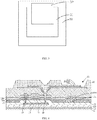
FIG. 1 is a schematic structural diagram of a display panel provided by an embodiment of the present disclosure. -
FIG. 2 is a schematic diagram of an orthographic projection of a display panel on a substrate along a stacking direction of a first electrode plate provided by an embodiment of the present disclosure. -
FIG. 3 is a schematic diagram of the orthographic projection of the display panel on the substrate along the stacking direction of the first electrode plate after changing a position of a light-shielding conductive layer in the display panel provided inFIG. 2 . -
FIG. 4 is a schematic structural diagram of the display panel provided inFIG. 1 after adding a second transparent conductive layer. -
FIG. 5 is a schematic structural diagram of the display panel provided inFIG. 4 after changing a shape of the second transparent conductive layer. -
FIG. 6 is a schematic structural diagram of the display panel provided inFIG. 4 after changing a shape of the second transparent conductive layer. -
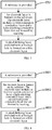
FIG. 7 is a program flow chart of a method for producing a display panel provided by an embodiment of the present disclosure. -
FIG. 8 is a program flow chart of the method for producing the display panel provided inFIG. 7 after adding a second transparent conductive layer. -
FIGs. 9 to 13 are schematic structural diagrams corresponding to each step in a method for producing a display panel provided by an embodiment of the present disclosure. - In order to make the objectives, technical solutions and advantages of the present disclosure clearer, the technical solutions in the embodiments of the present disclosure will be clearly and completely described with reference to the accompanying drawings in the present disclosure. It is evident that the embodiments described are only some rather than all embodiments in the present disclosure. Based on the embodiments of the present disclosure, all other embodiments obtained by those of ordinary skills in the art without any creative work shall fall within the protection scope of the present disclosure.
- An OLED display device has a problem that after reducing an area of an opaque electrode, it is easy to cause a display panel to emit light abnormally. According to the applicant's research, the reason for this problem is that the OLED display device in the existing technology is usually provided with a through hole on a pixel defining layer. In order to ensure a normal light emission, the through hole in the existing technology needs to fall on the opaque electrode. However, with a decrease of the opaque electrode, due to an existence of process errors, the through hole may not completely fall on the electrode, and the problem of abnormal display may occur at this time.
- An embodiment of the present disclosure relates to a display panel, as shown in
FIG. 1 , including: asubstrate 10, apixel defining layer 20 disposed on thesubstrate 10, and anelectrode layer 30 located between thesubstrate 10 and thepixel defining layer 20. Herein, thepixel defining layer 20 includes a throughhole 21 disposed opposite to theelectrode layer 30, and the throughhole 21 penetrates through thepixel defining layer 20 and falls on theelectrode layer 30. Theelectrode layer 30 includes a first transparentconductive layer 31 and a light-shieldingconductive layer 32 that are arranged in a stack. Along a stacking direction of theelectrode layer 30, an area of an orthographic projection of the first transparentconductive layer 31 on the substrate is larger than an area of an orthographic projection of the light-shieldingconductive layer 32 on the substrate. - The
electrode layer 30 is formed by stacking the first transparentconductive layer 31 and the light-shieldingconductive layer 32. A light transmittance of the firstconductive layer 31 is greater than a light transmittance of the light-shielding layer 32, and along the stacking direction of theelectrode layer 30, the area of the orthographic projection of the first transparentconductive layer 31 on the substrate is larger than the area of the orthographic projection of the light-shieldingconductive layer 32 on the substrate. Therefore, under the condition of having the same light transmittance (that is, an area of an opaque part is the same) as in the existing technology, theelectrode layer 30 in the embodiment of the present disclosure has a larger overall area along the stacking direction of theelectrode layer 30. Theelectrode layer 30 with a larger area makes the throughhole 21 less likely to fall outside theelectrode layer 30 when it is arranged in cooperation with theelectrode layer 30, thus reducing the possibility of abnormal light emission in the display panel. - As shown in
FIG. 2 , along the stacking direction of theelectrode layer 30, the orthographic projection of the light-shieldingconductive layer 32 on thesubstrate 10 is located inside the orthographic projection of the first transparentconductive layer 31 on thesubstrate 10. That is, an area where the light-shieldingconductive layer 32 is attached with the first transparentconductive layer 31 is at least the area of the orthographic projection of the light-shieldingconductive layer 32 on thesubstrate 10, so that a contact area between the first transparentconductive layer 31 and the light-shieldingconductive layer 32 is large, and the first transparentconductive layer 31 may better protect the light-shieldingconductive layer 32. - The orthographic projection of the light-shielding
conductive layer 32 on thesubstrate 10 is located inside the orthographic projection of the first transparentconductive layer 31 on thesubstrate 10, which is only a specific example of an arrangement state of the first transparentconductive layer 31 and the light-shieldingconductive layer 32 in this embodiment. As shown inFIG. 3 , along the stacking direction of theelectrode layer 30, the orthographic projection of the light-shieldingconductive layer 32 on thesubstrate 10 may also partially overlap with the orthographic projection of the first transparentconductive layer 31 on thesubstrate 10. Along the stacking direction of theelectrode layers 30, the orthographic projection of the light-shieldingconductive layer 32 on thesubstrate 10 partially overlaps with the orthographic projection of the first transparentconductive layer 31 on thesubstrate 10, so that the overall area of theelectrode layer 30 is larger than an overall area of the first transparentconductive layer 31, thereby further increasing the overall area of theelectrode layer 30 and further reducing the possibility of abnormal light emission. - A material of the first transparent
conductive layer 31 is ITO or IZO, and a material of the light-shieldingconductive layer 32 is a metal or a graphite, where the metal may be a silver, a lead, etc. The material of the first transparentconductive layer 31 being the ITO or the IZO is only a specific example of the material of the first transparentconductive layer 31 in this embodiment, and does not constitute a limitation. In other embodiments of the present disclosure, the first transparentconductive layer 31 may also be other materials with both transparent and conductive properties, such as ZnO-based TCO, etc., which are not listed here. In addition, the material of the light-shieldingconductive layer 32 being the metal or the graphite is only a specific example of the material of the light-shieldingconductive layer 32 in this embodiment and does not constitute a limitation. In other embodiments of the present disclosure, the light-shieldingconductive layer 32 may also be other materials with both light-shielding and conductive properties, such as an opaque conductive plastic, etc., which are not listed here, but may be flexibly selected according to actual needs. - The first transparent
conductive layer 31 is sandwiched between thesubstrate 10 and the light-shieldingconductive layer 32. The light-shieldingconductive layer 32 is located on a surface of the first transparentconductive layer 31 facing thesubstrate 10. Since the light-shieldingconductive layer 32 made of the metal and other materials has a poor bonding with thesubstrate 10, in this embodiment, the first transparentconductive layer 31 made of the ITO or the IZO material is sandwiched between thesubstrate 10 and the light-shieldingconductive layer 32, which may make the bonding between layers in the display panel firmer and improve the reliability of the display panel. - The above-described sandwiching the first transparent
conductive layer 31 between thesubstrate 10 and the light-shieldingconductive layer 32 is only an example of a positional relationship among the first transparentconductive layer 31, thesubstrate 10 and the light-shieldingconductive layer 32 in this embodiment, and does not constitute a limitation. In other embodiments of the present disclosure, the light-shieldingconductive layer 32 may also be sandwiched between thesubstrate 10 and the first transparentconductive layer 31. The light-shieldingconductive layer 32 made of the metal or the graphite is sandwiched between thesubstrate 10 and the first transparentconductive layer 31, so that the first transparentconductive layer 31 may protect the light-shieldingconductive layer 32 and prevent the light-shieldingconductive layer 32 from being oxidized. - The through
hole 21 falls on theelectrode layer 30. By setting the throughhole 21 to fall on theelectrode layer 30, the possibility of abnormal light emission of the display panel may be completely eliminated. In order to prevent the actually produced throughhole 21 from falling on a region outside theelectrode layer 30 due to a technical error, when designing a positional relationship between the throughhole 21 and theelectrode layer 30 in this embodiment, an error reserve area is set at an edge of theelectrode layer 30 in advance, that is, a part of theelectrode layer 30 close to the edge is set as the error reserve area. When designing the positional relationship between the throughhole 21 and theelectrode layer 30, a position of the throughhole 21 is not set to the error reserve area. - The error reserve area is an area with a distance less than 2µm from the edge of the
electrode layer 30. The above is only a specific example of the error reserve area in this embodiment. In other embodiments of the present disclosure, the error reserve area may also be of other sizes, which may be flexibly set according to actual needs. - A sidewall of the through
hole 21 at least partially falls on the first transparentconductive layer 31. The sidewall of the throughhole 21 at least partially falling on the first transparentconductive layer 31 is only an example of a specific position in this embodiment, and does not constitute a limitation. In other embodiments of the present disclosure, the sidewall of the throughhole 21 may not fall on the first transparentconductive layer 31, but fall on other parts of theelectrode layer 30, such as all falling on the light-shieldingconductive layer 32, which is not listed here. In this embodiment, theelectrode layer 30 is an anode layer. - The
substrate 10 sequentially includes aunderlay 11, abarrier layer 12 located above theunderlay 11, abuffer layer 13 located above thebarrier layer 12, achannel 14 located above thebuffer layer 13, a firstgate insulating layer 15 covering thechannel 14, agate 16 disposed above the firstgate insulating layer 15 and asource 17 and adrain 18 penetrating through the firstgate insulating layer 15, a secondgate insulating layer 19 located above the firstgate insulating layer 15 and covering thegate 16, an intermediate insulating layer 10a covering the secondgate insulating layer 19, afilling layer 10b covering the intermediate insulating layer 10a, a capacitorlower plate 10c located between the firstgate insulating layer 15 and the secondgate insulating layer 19, and a capacitorupper plate 10d located between the intermediate insulating layer 10a and the secondgate insulating layer 19. - The
electrode layer 30 is disposed on thefilling layer 10b and electrically connected to thedrain 18 through thefilling layer 10b. - A material of the
filling layer 10b is a polylactic acid. The material of thefilling layer 10b being the polylactic acid is only a specific example in this embodiment. In other embodiments of the present disclosure, thefilling layer 10b may also be made of other materials, such as a polyethylene, which are not listed here, but may be flexibly set according to actual needs. - An embodiment of the present disclosure also relates to a display panel, which is substantially the same as the previous embodiments and also includes a
substrate 10, apixel defining layer 20 disposed on thesubstrate 10, and anelectrode layer 30 located between thesubstrate 10 and thepixel defining layer 20. Herein, thepixel defining layer 20 includes a throughhole 21 disposed opposite to theelectrode layer 30, and the throughhole 21 penetrates through thepixel defining layer 20 and falls on theelectrode layer 30. The main difference is that in this embodiment, as shown inFIG. 4 , theelectrode layer 30 includes a second transparentconductive layer 33 in addition to a firsttransparent electrode layer 31 and a light-shieldingconductive layer 32. A material of the second transparentconductive layer 33 is ITO or IZO. The material of the second transparentconductive layer 33 being the ITO or the IZO is only a specific example of the material of the second transparentconductive layer 33 in this embodiment, and does not constitute a limitation. In other embodiments of the present disclosure, the second transparentconductive layer 33 may also be other materials with both transparent and conductive properties, such as ZnO-based TCO, which are not listed here. - The first transparent
conductive layer 31 is sandwiched between the light-shieldingconductive layer 32 and thesubstrate 10, and the light-shieldingconductive layer 32 is sandwiched between the first transparentconductive layer 31 and the second transparentconductive layer 33. The light-shieldingconductive layer 32 is located on a surface of the first transparentconductive layer 31 facing the second transparentconductive layer 33, and the light-shieldingconductive layer 32 is located on a surface of the second transparentconductive layer 33 facing the first transparentconductive layer 31. - While retaining all the technical effects of the display panel provided by the previous embodiment, the display panel provided by the present embodiment is further provided with the
electrode layer 30 including the second transparentconductive layer 33 and the light-shieldingconductive layer 32 sandwiched between the first transparentconductive layer 31 and the second transparentconductive layer 33, which may effectively increase a firmness of the combination between various components and improve the reliability of the display panel; and may also protect the light-shieldingconductive layer 32 and prevent the light-shieldingconductive layer 32 from being oxidized. - A sidewall of the through
hole 21 at least partially falls on the first transparentconductive layer 31. The sidewall of the throughhole 21 at least partially falling on the first transparentconductive layer 31 is only an example of a specific position in this embodiment, and does not constitute a limitation. In other embodiments of the present disclosure, the sidewall of the throughhole 21 may not fall on the first transparentconductive layer 31, but fall on other parts of theelectrode layer 30, such as all falling on the second transparentconductive layer 33 or all falling on the light-shielding conductive layer; or the sidewall of the throughhole 21 may also at least partially fall on the light-shieldingconductive layer 32; or the sidewall of the throughhole 21 may also at least partially fall on the second transparentconductive layer 33, which are not listed here. - An area of the second transparent
conductive layer 33 is equal to an area of the light-shieldingconductive layer 32 along a stacking direction of theelectrode layer 30. The area of the second transparentconductive layer 33 being equal to the area of the light-shieldingconductive layer 32 is only a specific application example in this embodiment, which does not constitute a limitation. In other embodiments of the present disclosure, as shown inFIG. 5 , the area of the second transparentconductive layer 33 may be larger than the area of the light-shieldingconductive layer 32, even if the second transparentconductive layer 33 completely covers an upper surface and a side surface of the light-shieldingconductive layer 32. Alternatively, as shown inFIG. 6 , the area of the second transparentconductive layer 33 may be smaller than the area of light-shieldingconductive layer 32, that is, part of the upper surface of the light-shieldingconductive layer 32 is exposed. - A thickness of the first transparent
conductive layer 31 and a thickness of the second transparentconductive layer 33 are both greater than or equal to 8 nm and less than or equal to 15 nm. The thickness of the first transparentconductive layer 31 and the thicknesses of the second transparentconductive layer 33 may be the same or different. - The thickness of the first transparent
conductive layer 31 and the thicknesses of the second transparentconductive layer 33 are both 10 nm. - A thickness of the light-shielding
conductive layer 32 is greater than or equal to 80 nm and less than or equal to 120 nm. - The thickness of the light-shielding
conductive layer 32 is 100 nm. - An embodiment of the present disclosure relates to a display device, which includes the display panel provided by other embodiments of the present disclosure.
- The display device provided by the embodiment of the present disclosure includes the display panel provided by other embodiments of the present disclosure. Therefore, the display device provided by this embodiment has all the technical effects of the display panel provided by other embodiments of the present disclosure, which is not repeated here.
- An embodiment of the present disclosure relates to a method for producing a display panel, as shown in
FIG. 7 , which includes the following steps. - In S701, a substrate is provided.
- In S702, an electrode layer is formed on the substrate. The electrode layer includes a first transparent conductive layer and a light-shielding conductive layer that are formed by stacking.
- The first transparent conductive layer and the light-shielding conductive layer are formed on the substrate by stacking to serve as the electrode layer. A projection area of the first transparent conductive layer is larger than a projection area of the light-shielding conductive layer in a stacking direction of the electrode layer.
- In S703, a pixel defining layer is formed on the electrode layer.
- The pixel defining layer is internally provided with a through hole disposed opposite to the electrode layer, and the through hole penetrates through the pixel defining layer and falls on the electrode layer. The through hole falls on the electrode layer, that is, side walls of the through hole all fall on the electrode layer.
- In order to prevent an edge of the actually produced through hole from falling on a region outside the electrode layer due to a technical error, when designing a position of the through hole in this embodiment, a preset position of the through hole is a region away from an edge of the electrode layer by a preset distance.
- The preset distance is less than 3µm. The preset distance is 2µm. The preset distance being 2µm is only a specific example in this embodiment, and does not constitute a limitation. In other embodiments of the present disclosure, the preset distance may also be other values, which are not listed here, but may be flexibly set according to actual needs.
- This embodiment is an embodiment of the method for producing the display panel corresponding to the embodiments mentioned above, and this embodiment may be implemented in cooperation with the embodiments mentioned above. The relevant technical details mentioned in the above-mentioned embodiments are still valid in this embodiment, and in order to reduce repetition, they will not be repeated here. Correspondingly, the relevant technical details mentioned in this embodiment may also be applied in the above-mentioned embodiments.
- The display panel prepared by the method for producing the display panel provided by the embodiment of the present disclosure increases an anode area, where an increased anode area is a transparent ITO or IZO film which has almost no influence on a light transmittance of a screen body, and fundamentally prevents an effect that the pixel defining layer is unable to completely wrap the anode, thereby greatly increasing a process allowance of wrapping the anode with the pixel defining layer, effectively reducing a requirement on an alignment accuracy of the pixel defining layer and the anode, and simplifying the process steps.
- An embodiment of the present disclosure relates to a method for producing a display panel, as shown in
FIG. 8 , which includes the following steps. - In S801, a substrate is provided.
- In S802, an electrode layer is formed on the substrate. The electrode layer includes a first transparent conductive layer, a light-shielding conductive layer, and a second transparent conductive layer that are formed by stacking.
- The electrode layer is formed on the substrate, which specifically includes the following steps.
- As shown in
FIG. 9 , a first transparentconductive layer 31 is formed on the substrate, a light-shieldingconductive layer 32 covering the first transparentconductive layer 31 is formed on the first transparentconductive layer 31, a second transparentconductive layer 33 covering the light-shieldingconductive layer 32 is formed on the second transparentconductive layer 33, and aphotoresist layer 40 covering the second transparentconductive layer 33 is formed on the second transparentconductive layer 33. - As shown in
FIG. 10 , the photoresist layer is patterned. Afirst photoresist region 331, asecond photoresist region 332 and a photoresist-free region 333 are formed on the second transparentconductive layer 33 in parallel. - The photoresist layer is patterned through an exposure and development process using a semi light-
transmissive mask 50. The semi light-transmissive mask 50 includes a fully light-transmissive region 51, a semi light-transmissive region 52 and an opticallyopaque region 53. A transparency of the semi light-transmissive region 52 is greater than a transparency of the opticallyopaque region 53 but less than a transparency of the fully light-transmissive region 51. Thefirst photoresist region 331 is formed below the opticallyopaque region 53, thesecond photoresist region 332 is formed below the semi light-transmissive region 52, and the photoresist-free region 333 is formed below fully light-transmissive region 51. - Herein, a thickness of a photoresist layer on a surface of the
second photoresist region 332 is smaller than a thickness of a photoresist layer on a surface of thefirst photoresist region 331. - As shown in
FIG. 11 , the first transparentconductive layer 31, the light-shieldingconductive layer 32 and the second transparentconductive layer 33 in the photoresist-free region are removed. - The first transparent
conductive layer 31 and the second transparentconductive layer 33 are etched using an oxalic acid etching solution. The light-shieldingconductive layer 32 is etched using a mixed acid etching solution of HNO3, CH3COOH, and H3PO4. - As shown in
FIG. 12 , the photoresist layer on the surface of thesecond photoresist region 332 is removed. - A reaction is carried out by using SF6+O2 gas through a dry ashing process to remove the photoresist layer on the surface of the
first photoresist region 332. In addition, aphotoresist layer 40 on the surface of thesecond photoresist region 333 also reacts and decreases, resulting in a decrease in the thickness of thephotoresist layer 40 on the surface of thesecond photoresist region 333. - As shown in
FIG. 13 , the light-shieldingconductive layer 32 and the second transparentconductive layer 33 in the second photoresist region are removed, and the photoresist layer on the surface of thefirst photoresist region 331 is removed. - In this step, the second transparent conductive layer and the light-shielding conductive layer which are not shielded by the photoresist layer are removed by a two-step wet etching.
- The second transparent
conductive layer 33 is etched using the oxalic acid etching solution. The light-shieldingconductive layer 32 is etched using the mixed acid etching solution of HNO3, CH3COOH, and H3PO4. - The photoresist layer on the surface of the second photoresist region is removed by the dry ashing process.
- In S803, a pixel defining layer is formed on the electrode layer.
- Since S801 and S803 in this embodiment are substantially the same as S701 and S703 in the forgoing embodiment, the specific content of the forgoing embodiment may be specifically referred to, which is not repeated here.
- It is not difficult to find that this embodiment is an embodiment of the method for producing the display panel corresponding to the embodiments mentioned above, and this embodiment may be implemented in cooperation with the embodiments mentioned above. The relevant technical details mentioned in the above-mentioned embodiments are still valid in this embodiment, and in order to reduce repetition, they will not be repeated here. Correspondingly, the relevant technical details mentioned in this embodiment may also be applied in the above-mentioned embodiments.
- Compared with the existing technology, the display panel prepared by the method for producing the display panel provided by the embodiment of the present disclosure, by proposing a new method or solution of an anode reticle mask, achieves an effect of increasing an anode area, where an increased anode area is a transparent ITO or IZO film which has almost no influence on a light transmittance of a screen body, and fundamentally preventing the pixel defining layer from being unable to completely cover the anode, so as to meet a process limit demand that an under-screen fingerprint identification technology is widely used in a display panel product without adding an extra reticle.
- Those skilled in the art should appreciate that the aforementioned embodiments are specific embodiments for implementing the present disclosure. In practice, however, various changes may be made in the forms and details of the specific embodiments without departing from the spirit and scope of the present disclosure.
Claims (20)
- A display panel, comprising:a substrate;a pixel defining layer disposed on the substrate; andan electrode layer located between the substrate and the pixel defining layer;wherein the pixel defining layer is internally provided with a through hole disposed opposite to the electrode layer, and the through hole penetrates through the pixel defining layer and falls on the electrode layer;the electrode layer comprises a first transparent conductive layer and a light-shielding conductive layer that are arranged in a stack, and along a stacking direction of the electrode layer, an area of an orthographic projection of the first transparent conductive layer on the substrate is larger than an area of an orthographic projection of the light-shielding conductive layer on the substrate.
- The display panel according to claim 1, wherein along the stacking direction of the electrode layer, the orthographic projection of the light-shielding conductive layer on the substrate is located inside the orthographic projection of the first transparent conductive layer on the substrate.
- The display panel according to claim 1, wherein along the stacking direction of the electrode layer, the orthographic projection of the light-shielding conductive layer on the substrate partially overlaps with the orthographic projection of the first transparent conductive layer on the substrate.
- The display panel according to claim 1, wherein the light-shielding conductive layer is sandwiched between the substrate and the first transparent conductive layer.
- The display panel according to claim 4, wherein the light-shielding conductive layer is located on a surface of the first transparent conductive layer facing the substrate.
- The display panel according to claim 1, wherein the first transparent conductive layer is sandwiched between the substrate and the light-shielding conductive layer.
- The display panel according to claim 6, wherein the first transparent conductive layer is located on a surface of the light-shielding conductive layer facing the substrate.
- The display panel according to claim 1, wherein the electrode layer further comprises a second transparent conductive layer, and the light-shielding conductive layer is sandwiched between the first transparent conductive layer and the second transparent conductive layer.
- The display panel according to claim 8, wherein the light-shielding conductive layer is located on a surface of the first transparent conductive layer facing the second transparent conductive layer, and the light-shielding conductive layer is located on a surface of the second transparent conductive layer facing the first transparent conductive layer.
- The display panel according to claim 8, wherein a sidewall of the through hole at least partially falls on the first transparent conductive layer.
- The display panel according to claim 8, wherein a sidewall of the through hole at least partially falls on the light-shielding conductive layer.
- The display panel according to claim 8, wherein a sidewall of the through hole at least partially falls on the second transparent conductive layer.
- The display panel according to claim 8, wherein a material of the first transparent conductive layer is ITO or IZO, a material of the second transparent conductive layer is ITO or IZO, and a material of the light-shielding conductive layer is a metal or a graphite.
- The display panel according to claim 8, wherein a thicknesses of the first transparent conductive layer and a thicknesses of the second transparent conductive layer are both greater than or equal to 8 nm and less than or equal to 15 nm.
- The display panel according to claim 8, wherein a thickness of the light-shielding conductive layer is greater than or equal to 80 nm and less than or equal to 120 nm.
- A display device, comprising the display panel according to any one of claims 1 to 15.
- A method for producing a display panel, comprising the following steps:providing a substrate;forming an electrode layer on the substrate; andforming a pixel defining layer on the electrode layer, wherein the pixel defining layer is internally provided with a through hole disposed opposite to the electrode layer, and the through hole penetrates through the pixel defining layer and falls on the electrode layer;wherein forming the electrode layer on the substrate specifically comprises forming a first transparent conductive layer and a light-shielding conductive layer on the substrate by stacking,and along a stacking direction of the electrode layer, an area of an orthographic projection of the first transparent conductive layer on the substrate is larger than an area of an orthographic projection of the light-shielding conductive layer on the substrate.
- The method for producing the display panel according to claim 17, wherein forming the electrode layer on the substrate further comprises forming a second transparent conductive layer on a surface of the light-shielding conductive layer away from the first transparent conductive layer.
- The method for producing the display panel according to claim 18, wherein forming the electrode layer on the substrate specifically comprises:S1: forming the first transparent conductive layer on the substrate, forming the light-shielding conductive layer on the first transparent conductive layer, forming the second transparent conductive layer on the light-shielding conductive layer and forming a photoresist layer on the second transparent conductive layer;S2: patterning the photoresist layer, forming a first photoresist region, a second photoresist region and a photoresist-free region on the second transparent conductive layer, wherein a thickness of a photoresist layer on a surface of the second photoresist region is smaller than a thickness of a photoresist layer on a surface of the first photoresist region;S3: removing the first transparent conductive layer, the light-shielding conductive layer and the second transparent conductive layer in the photoresist-free region;S4: removing the photoresist layer on the surface of the second photoresist region;S5: removing the light-shielding conductive layer and the second transparent conductive layer in the second photoresist region; andS6: removing the photoresist layer on the surface of the first photoresist region.
- The method for producing the display panel according to claim 19, wherein patterning the photoresist layer, forming the first photoresist region, the second photoresist region and the photoresist-free region on the second transparent conductive layer specifically comprises:patterning the photoresist layer by using a mask;wherein the mask comprises a fully light-transmissive region, a semi light-transmissive region and an optically opaque region, a transparency of the semi light-transmissive region is greater than a transparency of the optically opaque region but less than a transparency of the fully light-transmissive region; the photoresist-free region is formed below the fully light-transmissive region, the second photoresist region is formed below the semi light-transmissive region, and the first photoresist region is formed below the optically opaque region.
Applications Claiming Priority (2)
| Application Number | Priority Date | Filing Date | Title |
|---|---|---|---|
| CN201910458204.2A CN110165079B (en) | 2019-05-29 | 2019-05-29 | Display panel, manufacturing method thereof and display device |
| PCT/CN2019/119000 WO2020238071A1 (en) | 2019-05-29 | 2019-11-15 | Display panel and preparation method therefor, and display device |
Publications (2)
| Publication Number | Publication Date |
|---|---|
| EP3876297A1 true EP3876297A1 (en) | 2021-09-08 |
| EP3876297A4 EP3876297A4 (en) | 2022-01-12 |
Family
ID=67630073
Family Applications (1)
| Application Number | Title | Priority Date | Filing Date |
|---|---|---|---|
| EP19931277.8A Pending EP3876297A4 (en) | 2019-05-29 | 2019-11-15 | DISPLAY BOARD AND METHOD FOR PREPARING IT, AND DISPLAY DEVICE |
Country Status (7)
| Country | Link |
|---|---|
| US (1) | US12022674B2 (en) |
| EP (1) | EP3876297A4 (en) |
| JP (1) | JP7197704B2 (en) |
| KR (1) | KR102547608B1 (en) |
| CN (1) | CN110165079B (en) |
| TW (1) | TWI720704B (en) |
| WO (1) | WO2020238071A1 (en) |
Families Citing this family (2)
| Publication number | Priority date | Publication date | Assignee | Title |
|---|---|---|---|---|
| CN110165079B (en) * | 2019-05-29 | 2020-08-25 | 昆山国显光电有限公司 | Display panel, manufacturing method thereof and display device |
| CN115394802A (en) * | 2021-05-06 | 2022-11-25 | 金佶科技股份有限公司 | Image capturing device |
Family Cites Families (24)
| Publication number | Priority date | Publication date | Assignee | Title |
|---|---|---|---|---|
| JP4497881B2 (en) | 2003-09-30 | 2010-07-07 | 三洋電機株式会社 | Organic EL device and organic EL panel |
| KR100714011B1 (en) * | 2005-11-30 | 2007-05-04 | 삼성에스디아이 주식회사 | Flat Panel Display and Manufacturing Method |
| KR100796618B1 (en) | 2007-01-04 | 2008-01-22 | 삼성에스디아이 주식회사 | Organic light emitting display device and manufacturing method |
| JP5411469B2 (en) | 2008-08-28 | 2014-02-12 | セイコーエプソン株式会社 | LIGHT EMITTING DEVICE AND ELECTRONIC DEVICE |
| US20100051973A1 (en) * | 2008-08-28 | 2010-03-04 | Seiko Epson Corporation | Light-emitting device, electronic equipment, and process of producing light-emitting device |
| CN102668706B (en) * | 2009-11-17 | 2015-03-25 | 联合创新技术有限公司 | Organic el display |
| WO2011114424A1 (en) | 2010-03-15 | 2011-09-22 | パイオニア株式会社 | Organic el panel and method for producing same |
| JP2014078536A (en) | 2010-03-15 | 2014-05-01 | Pioneer Electronic Corp | Organic el device |
| CN103474448A (en) * | 2013-08-30 | 2013-12-25 | 京东方科技集团股份有限公司 | Electroluminescent device and display device |
| KR102148935B1 (en) * | 2013-11-21 | 2020-08-31 | 삼성디스플레이 주식회사 | Organic light emitting diode display device and method of manufacturing the same |
| JP2015138612A (en) * | 2014-01-21 | 2015-07-30 | 株式会社ジャパンディスプレイ | Organic electroluminescence display device |
| JP6204209B2 (en) | 2014-01-27 | 2017-09-27 | 株式会社ジャパンディスプレイ | Organic EL display device |
| KR102313362B1 (en) * | 2014-12-02 | 2021-10-18 | 삼성디스플레이 주식회사 | Organic light-emitting display apparatus and method for manufacturing the same |
| JP2016149191A (en) * | 2015-02-10 | 2016-08-18 | 株式会社ジャパンディスプレイ | Organic EL display device |
| JP6517597B2 (en) * | 2015-06-10 | 2019-05-22 | 株式会社ジャパンディスプレイ | Display device |
| CN105552249B (en) * | 2016-03-16 | 2017-11-14 | 京东方科技集团股份有限公司 | Oled display substrate and preparation method thereof, display device |
| KR102651060B1 (en) * | 2016-08-11 | 2024-03-26 | 삼성디스플레이 주식회사 | Organic light emitting display device |
| CN106531768A (en) * | 2016-12-07 | 2017-03-22 | 厦门天马微电子有限公司 | Organic electroluminescence display panel and preparation method thereof |
| WO2018173465A1 (en) | 2017-03-21 | 2018-09-27 | ソニーセミコンダクタソリューションズ株式会社 | Light emitting element, display device and electronic device |
| CN107706209B (en) * | 2017-08-09 | 2019-06-25 | 武汉华星光电半导体显示技术有限公司 | Organic electroluminescent display panel and preparation method thereof |
| CN107706221B (en) | 2017-09-28 | 2019-11-26 | 深圳市华星光电半导体显示技术有限公司 | The production method and OLED display of OLED display |
| US20190206963A1 (en) * | 2017-12-29 | 2019-07-04 | Shenzhen China Star Optoelectronics Semiconductor Display Technology Co., Ltd. | Display panel and method for manufacturing the same |
| CN109742114B (en) * | 2019-01-08 | 2021-01-26 | 京东方科技集团股份有限公司 | Display back plate manufacturing method, display back plate and display device |
| CN110165079B (en) * | 2019-05-29 | 2020-08-25 | 昆山国显光电有限公司 | Display panel, manufacturing method thereof and display device |
-
2019
- 2019-05-29 CN CN201910458204.2A patent/CN110165079B/en active Active
- 2019-11-15 WO PCT/CN2019/119000 patent/WO2020238071A1/en not_active Ceased
- 2019-11-15 KR KR1020217017597A patent/KR102547608B1/en active Active
- 2019-11-15 JP JP2021534680A patent/JP7197704B2/en active Active
- 2019-11-15 EP EP19931277.8A patent/EP3876297A4/en active Pending
- 2019-11-27 TW TW108143105A patent/TWI720704B/en active
-
2021
- 2021-05-26 US US17/330,676 patent/US12022674B2/en active Active
Also Published As
| Publication number | Publication date |
|---|---|
| KR20210078562A (en) | 2021-06-28 |
| US12022674B2 (en) | 2024-06-25 |
| TWI720704B (en) | 2021-03-01 |
| CN110165079A (en) | 2019-08-23 |
| CN110165079B (en) | 2020-08-25 |
| EP3876297A4 (en) | 2022-01-12 |
| KR102547608B1 (en) | 2023-06-26 |
| WO2020238071A1 (en) | 2020-12-03 |
| JP7197704B2 (en) | 2022-12-27 |
| JP2022514563A (en) | 2022-02-14 |
| TW202013715A (en) | 2020-04-01 |
| US20210280816A1 (en) | 2021-09-09 |
Similar Documents
| Publication | Publication Date | Title |
|---|---|---|
| US11575108B2 (en) | Display panel, preparation method thereof, and display device | |
| US11315977B2 (en) | Photosensitive assembly and method for preparing the same, array substrate, and display device | |
| US11302681B2 (en) | Display device and method of manufacturing thereof | |
| CN108091675B (en) | Display substrate and manufacturing method thereof | |
| US11527738B2 (en) | Display substrate comprising metal layer structure in non-display region and with recessed side surface,preparation method thereof, and display device | |
| EP3678205A1 (en) | Oled display mother board and manufacturing method thereof, manufacturing method of oled display panel and oled display device thereof | |
| KR101701229B1 (en) | Display substrate and method of manufacturing the same | |
| KR102810223B1 (en) | Display device | |
| US20190393289A1 (en) | Display panel and method of manufacturing thereof | |
| US10651244B2 (en) | Touch display panel, method for fabricating the same, and display device | |
| US20190034012A1 (en) | Touch substrate, manufacturing method thereof and touch device | |
| CN107887527A (en) | OLED display panel and preparation method, encapsulation part failure determination methods, display device | |
| CN107623009A (en) | Preparation method, array base palte and the display device of array base palte | |
| CN109801953B (en) | Organic light emitting diode display substrate, preparation method and device thereof | |
| KR20200035239A (en) | Display panel, manufacturing method and display module | |
| US12022674B2 (en) | Display panel and method for producing same, and display device | |
| CN111474755A (en) | Display module, method for making the same, and display device | |
| WO2023193296A1 (en) | Display panel and display apparatus | |
| CN111477664A (en) | Display panel, manufacturing method thereof and display device | |
| CN107845737A (en) | Display panel, manufacturing method thereof and display device | |
| US10312266B2 (en) | Display substrate and manufacturing method thereof, and display device | |
| KR101690600B1 (en) | Display Device With Integrated Touch Screen and Method for Manufacturing The Same | |
| CN104393020B (en) | A kind of array base palte and preparation method thereof, display device | |
| KR102010851B1 (en) | Organic Light Emitting Diode Display Device And Method Manufacturing The Same | |
| CN117044427A (en) | Display panel, display motherboard and display device |
Legal Events
| Date | Code | Title | Description |
|---|---|---|---|
| STAA | Information on the status of an ep patent application or granted ep patent |
Free format text: STATUS: THE INTERNATIONAL PUBLICATION HAS BEEN MADE |
|
| PUAI | Public reference made under article 153(3) epc to a published international application that has entered the european phase |
Free format text: ORIGINAL CODE: 0009012 |
|
| STAA | Information on the status of an ep patent application or granted ep patent |
Free format text: STATUS: REQUEST FOR EXAMINATION WAS MADE |
|
| 17P | Request for examination filed |
Effective date: 20210603 |
|
| AK | Designated contracting states |
Kind code of ref document: A1 Designated state(s): AL AT BE BG CH CY CZ DE DK EE ES FI FR GB GR HR HU IE IS IT LI LT LU LV MC MK MT NL NO PL PT RO RS SE SI SK SM TR |
|
| A4 | Supplementary search report drawn up and despatched |
Effective date: 20211209 |
|
| RIC1 | Information provided on ipc code assigned before grant |
Ipc: H01L 21/77 20170101ALI20211203BHEP Ipc: H01L 27/32 20060101ALI20211203BHEP Ipc: H01L 51/52 20060101AFI20211203BHEP |
|
| DAV | Request for validation of the european patent (deleted) | ||
| DAX | Request for extension of the european patent (deleted) | ||
| STAA | Information on the status of an ep patent application or granted ep patent |
Free format text: STATUS: EXAMINATION IS IN PROGRESS |
|
| 17Q | First examination report despatched |
Effective date: 20240405 |
|
| REG | Reference to a national code |
Ref country code: DE Ref legal event code: R079 Free format text: PREVIOUS MAIN CLASS: H01L0051520000 Ipc: H10K0059122000 |
|
| GRAP | Despatch of communication of intention to grant a patent |
Free format text: ORIGINAL CODE: EPIDOSNIGR1 |
|
| STAA | Information on the status of an ep patent application or granted ep patent |
Free format text: STATUS: GRANT OF PATENT IS INTENDED |
|
| RIC1 | Information provided on ipc code assigned before grant |
Ipc: H10K 59/122 20230101AFI20260326BHEP Ipc: H10K 59/80 20230101ALI20260326BHEP Ipc: H10K 59/65 20230101ALN20260326BHEP |
|
| INTG | Intention to grant announced |
Effective date: 20260408 |