EP3872865A1 - Schottky barrier diode - Google Patents
Schottky barrier diode Download PDFInfo
- Publication number
- EP3872865A1 EP3872865A1 EP19875151.3A EP19875151A EP3872865A1 EP 3872865 A1 EP3872865 A1 EP 3872865A1 EP 19875151 A EP19875151 A EP 19875151A EP 3872865 A1 EP3872865 A1 EP 3872865A1
- Authority
- EP
- European Patent Office
- Prior art keywords
- drift layer
- outer peripheral
- schottky barrier
- anode electrode
- barrier diode
- Prior art date
- Legal status (The legal status is an assumption and is not a legal conclusion. Google has not performed a legal analysis and makes no representation as to the accuracy of the status listed.)
- Pending
Links
Images







Classifications
-
- H—ELECTRICITY
- H10—SEMICONDUCTOR DEVICES; ELECTRIC SOLID-STATE DEVICES NOT OTHERWISE PROVIDED FOR
- H10D—INORGANIC ELECTRIC SEMICONDUCTOR DEVICES
- H10D62/00—Semiconductor bodies, or regions thereof, of devices having potential barriers
- H10D62/10—Shapes, relative sizes or dispositions of the regions of the semiconductor bodies; Shapes of the semiconductor bodies
- H10D62/102—Constructional design considerations for preventing surface leakage or controlling electric field concentration
- H10D62/103—Constructional design considerations for preventing surface leakage or controlling electric field concentration for increasing or controlling the breakdown voltage of reverse-biased devices
- H10D62/105—Constructional design considerations for preventing surface leakage or controlling electric field concentration for increasing or controlling the breakdown voltage of reverse-biased devices by having particular doping profiles, shapes or arrangements of PN junctions; by having supplementary regions, e.g. junction termination extension [JTE]
- H10D62/106—Constructional design considerations for preventing surface leakage or controlling electric field concentration for increasing or controlling the breakdown voltage of reverse-biased devices by having particular doping profiles, shapes or arrangements of PN junctions; by having supplementary regions, e.g. junction termination extension [JTE] having supplementary regions doped oppositely to or in rectifying contact with regions of the semiconductor bodies, e.g. guard rings with PN or Schottky junctions
-
- H—ELECTRICITY
- H10—SEMICONDUCTOR DEVICES; ELECTRIC SOLID-STATE DEVICES NOT OTHERWISE PROVIDED FOR
- H10D—INORGANIC ELECTRIC SEMICONDUCTOR DEVICES
- H10D62/00—Semiconductor bodies, or regions thereof, of devices having potential barriers
- H10D62/80—Semiconductor bodies, or regions thereof, of devices having potential barriers characterised by the materials
-
- H—ELECTRICITY
- H10—SEMICONDUCTOR DEVICES; ELECTRIC SOLID-STATE DEVICES NOT OTHERWISE PROVIDED FOR
- H10D—INORGANIC ELECTRIC SEMICONDUCTOR DEVICES
- H10D62/00—Semiconductor bodies, or regions thereof, of devices having potential barriers
- H10D62/80—Semiconductor bodies, or regions thereof, of devices having potential barriers characterised by the materials
- H10D62/82—Heterojunctions
-
- H—ELECTRICITY
- H10—SEMICONDUCTOR DEVICES; ELECTRIC SOLID-STATE DEVICES NOT OTHERWISE PROVIDED FOR
- H10D—INORGANIC ELECTRIC SEMICONDUCTOR DEVICES
- H10D64/00—Electrodes of devices having potential barriers
- H10D64/60—Electrodes characterised by their materials
- H10D64/64—Electrodes comprising a Schottky barrier to a semiconductor
-
- H—ELECTRICITY
- H10—SEMICONDUCTOR DEVICES; ELECTRIC SOLID-STATE DEVICES NOT OTHERWISE PROVIDED FOR
- H10D—INORGANIC ELECTRIC SEMICONDUCTOR DEVICES
- H10D8/00—Diodes
- H10D8/60—Schottky-barrier diodes
-
- H—ELECTRICITY
- H10—SEMICONDUCTOR DEVICES; ELECTRIC SOLID-STATE DEVICES NOT OTHERWISE PROVIDED FOR
- H10D—INORGANIC ELECTRIC SEMICONDUCTOR DEVICES
- H10D8/00—Diodes
- H10D8/60—Schottky-barrier diodes
- H10D8/605—Schottky-barrier diodes of the trench conductor-insulator-semiconductor barrier type, e.g. trench MOS barrier Schottky rectifiers [TMBS]
-
- H—ELECTRICITY
- H10—SEMICONDUCTOR DEVICES; ELECTRIC SOLID-STATE DEVICES NOT OTHERWISE PROVIDED FOR
- H10D—INORGANIC ELECTRIC SEMICONDUCTOR DEVICES
- H10D62/00—Semiconductor bodies, or regions thereof, of devices having potential barriers
- H10D62/10—Shapes, relative sizes or dispositions of the regions of the semiconductor bodies; Shapes of the semiconductor bodies
- H10D62/117—Shapes of semiconductor bodies
Definitions
- the present invention relates to a Schottky barrier diode and, more particularly, to a Schottky barrier diode using gallium oxide.
- a Schottky barrier diode is a rectifying element utilizing a Schottky barrier generated due to bonding between metal and a semiconductor and is lower in forward voltage and higher in switching speed than a normal diode having a PN junction.
- the Schottky barrier diode is sometimes utilized as a switching element for a power device.
- gallium oxide has a very large band gap (4.8 eV to 4.9 eV) and a large breakdown field (7 MV/cm to 8 MV/cm) , so that a Schottky barrier diode using gallium oxide is very promising as the switching element for a power device.
- An example of the Schottky barrier diode using gallium oxide is described in Patent Documents 1 to 3.
- Patent Document 1 discloses a Schottky barrier diode having a field plate structure.
- a Schottky barrier diode described in Patent Document 2 has a structure in which a plurality of trenches are provided so as to overlap an anode electrode in a plan view, and the inner wall of each of the plurality of trenches is covered with an insulating film.
- a p-type oxide semiconductor layer that covers a drift layer through a nitride layer is provided to form a depletion layer in the drift layer to thereby increase a withstand voltage upon application of a backward voltage.
- a Schottky barrier diode includes: a semiconductor substrate made of gallium oxide; a drift layer made of gallium oxide and provided on the semiconductor substrate; an anode electrode brought into Schottky contact with the drift layer; and a cathode electrode brought into ohmic contact with the semiconductor substrate.
- the drift layer has an outer peripheral trench surrounding the anode electrode in a plan view. The surface of the drift layer positioned between the anode electrode and the outer peripheral trench is covered with a semiconductor layer having a conductivity type opposite to that of the drift layer.
- the surface of the drift layer is covered with a semiconductor layer having an opposite conductivity type, so that when a backward voltage is applied, a depletion layer extends around in a part of the drift layer that is covered with the opposite conductivity type semiconductor layer.
- This relaxes concentration of an electric field on the corner portion of the anode electrode.
- the electric field concentrating on the end portion of the semiconductor layer is dispersed by the outer peripheral trench, alleviating electric field concentration on a part of the drift layer that overlaps the end portion of the semiconductor layer.
- the semiconductor layer may be made of an oxide semiconductor material. This can prevent a change in characteristics of the semiconductor layer due to oxidation.
- the anode electrode and the semiconductor layer may overlap each other. This can relax electric field concentration more effectively at the corner portion of the anode electrode.
- the outer peripheral trench may be filled with an insulating material or a semiconductor material having a conductivity type opposite to that of the drift layer.
- an electric force line extending in the drift layer can be blocked by the insulating material embedded in the outer peripheral trench, and in the latter case, there can be formed a depletion layer extending from the semiconductor material embedded in the outer peripheral trench to the drift layer.
- the drift layer may further have a plurality of center trenches formed at a position overlapping the anode electrode in a plan view.
- the inner wall of each of the plurality of center trenches may be covered with an insulating film.
- a Schottky barrier diode using gallium oxide which is less liable to cause dielectric breakdown due to concentration of an electric field.
- FIG. 1 is a schematic top view illustrating the configuration of a Schottky barrier diode 100 according to a first embodiment of the present invention.
- FIG. 2 is a schematic cross-sectional view taken along line A-A in FIG. 1 .
- the Schottky barrier diode 100 includes a semiconductor substrate 20 and a drift layer 30, both of which are made of gallium oxide ( ⁇ -Ga 2 O 3 ) .
- the semiconductor substrate 20 and the drift layer 30 are each introduced with silicon (Si) or tin (Sn) as an n-type dopant.
- the concentration of the dopant is higher in the semiconductor substrate 20 than in the drift layer 30, whereby the semiconductor substrate 20 and the drift layer 30 function as an n + layer and an n - layer, respectively.
- the semiconductor substrate 20 is obtained by cutting a bulk crystal formed using a melt-growing method, and the thickness (height in the Z-direction) thereof is about 250 ⁇ m.
- the planar size of the semiconductor substrate 20 is generally selected in accordance with the amount of current flowing in the element and, when the maximum amount of forward current is about 20 A, the widths in the X- and Y-directions may be set to about 2.4 mm.
- the semiconductor substrate 20 has an upper surface 21 positioned on the upper surface side and a back surface 22 positioned on the lower surface side, in a mounted state.
- the drift layer 30 is formed on the entire upper surface 21.
- the drift layer 30 is a thin film obtained by epitaxially growing gallium oxide on the upper surface 21 of the semiconductor substrate 20 using a reactive sputtering method, a PLD method, an MBE method, an MOCVD method, or an HVPE method.
- the film thickness of the drift layer 30 is generally selected in accordance with the backward withstand voltage of the element and may be set to, e.g., about 7 ⁇ m in order to ensure a withstand voltage of about 600 V.
- An anode electrode 40 is formed on an upper surface 31 of the drift layer 30 so as to be brought into Schottky contact with the drift layer 30.
- the anode electrode 40 is formed of metal such as platinum (Pt), palladium (Pd), gold (Au), nickel (Ni), or the like.
- the anode electrode 40 may have a multilayer structure of different metal films such as Pt/Au, Pt/Al, Pd/Au, Pd/Al, Pt/Ti/Au, or Pd/Ti/Au.
- a cathode electrode 50 is formed on the back surface 22 of the semiconductor substrate 20 so as to be brought into ohmic contact with the semiconductor substrate 20.
- the cathode electrode 50 is formed of metal such as titanium (Ti).
- the cathode electrode 50 may have a multilayer structure of different metal films such as Ti/Au or Ti/Al.
- the drift layer 30 has formed therein an outer peripheral trench 10 at a position not overlapping the anode electrode 40 in a plan view (as viewed in the Z-direction) so as to surround the anode electrode 40.
- the outer peripheral trench 10 can be formed by etching the drift layer 30 from the upper surface 31 side.
- the outer peripheral trench 10 is filled with an embedded layer 11.
- the embedded layer 11 may be an insulating material such as SiO 2 or a semiconductor material having a conductivity type opposite to that of the drift layer 30. That is, when the semiconductor material is used as the material of the embedded layer 11, a p-type semiconductor material needs to be selected since the conductivity type of the drift layer 30 is an n-type.
- the semiconductor material filled in the outer peripheral trench 10 may be in a floating state.
- a part of the surface of the drift layer 30 positioned between the anode electrode 40 and the outer peripheral trench 10 is covered with a semiconductor layer 70 having a conductivity type opposite to that of the drift layer 30.
- the drift layer 30 and the semiconductor layer 70 may directly contact each other, or may contact each other through an insulating film or the like. Since the conductivity type of the drift layer 30 is an n-type, the semiconductor layer 70 needs to be formed of a p-type semiconductor material.
- the p-type semiconductor material include Si, GaAs, SiC, Ge, ZnSe, CdS, InP, SiGe, and a p-type oxide semiconductor such as NiO, Cu 2 O, or Ag 2 O.
- the p-type semiconductor material has an advantage of being free from oxidation.
- NiO is a special material that exhibits only a p-type conductivity and is most preferable in terms of quality stabilization. Further, NiO has a band gap as large as 3.7 eV and is thus desirable as a material taking advantage of high withstand voltage of gallium oxide.
- Li or La may be added as a dopant in a ratio of about 0.2 mol% to 1.0 mol% to NiO (99.9%).
- the acceptor concentration is preferably equal to or higher than 5 ⁇ 10 17 cm -3 and more preferably equal to or higher than 5 ⁇ 10 18 cm -3 in terms of production stability.
- the semiconductor layer 70 may be in a floating state, or may contact the anode electrode 40 or the embedded layer 11 embedded in the outer peripheral trench 10.
- the surface of the semiconductor layer 70 is preferably covered with a passivation film of SiO 2 or the like.
- the p-type oxide constituting the semiconductor layer 70 is unintentionally crystallized in a heating process during device production, which may make the characteristics thereof unstable. Considering this, at the time when the p-type oxide is formed on the drift layer 30, about 50% by volume thereof may be crystallized, for example. This can reduce the influence of crystallization in a heat process during device production.
- the semiconductor layer 70 has a conductivity type opposite to that of the drift layer 30, a depletion layer extends around a part of the drift layer 30 that is covered with the semiconductor layer 70 due to a potential difference.
- a backward voltage is applied between the anode electrode 40 and the cathode electrode 50, an electric field concentrating on the end portion of the anode electrode 40 is relaxed.
- the electric field concentrating on the end portion of the anode electrode 40 is relaxed more effectively as a gap between the anode electrode 40 and the semiconductor layer 70 is smaller, so that the anode electrode 40 and the semiconductor layer 70 preferably contact each other.
- a part of the semiconductor layer 70 may be formed on the anode electrode 40 so as to cover the outer peripheral edge of the anode electrode 40 as in a Schottky barrier diode 100a according to a first modification ( FIG. 3 ).
- a part of the anode electrode 40 may be formed on the semiconductor layer 70 so as to cover the inner peripheral edge of the semiconductor layer 70 as in a Schottky barrier diode 100b according to a second modification ( FIG. 4 ).
- a gap G1 may exist between the outer peripheral edge of the anode electrode 40 and the inner peripheral edge of the semiconductor layer 70 as in a Schottky barrier diode 100c according to a third modification ( FIG. 5 ).
- the electric field concentrating on the end portion of the anode electrode 40 becomes stronger as the gap G1 is larger, so that the gap G1 should preferably be as small as possible.
- the electric field concentrating on the end portion of the anode electrode 40 is relaxed by providing the semiconductor layer 70.
- the electric field concentrates on the outer peripheral edge of the semiconductor layer 70, which, however, is relaxed by the outer peripheral trench 10.
- the electric field concentrating on the end portion of the anode electrode 40 is relaxed by the semiconductor layer 70, and the electric field concentrating on the outer peripheral edge of the semiconductor layer 70 is relaxed by the outer peripheral trench 10, thereby making it possible to prevent dielectric breakdown upon application of a backward voltage.
- the electric field concentrating on the outer peripheral edge of the semiconductor layer 70 is relaxed more effectively as a gap between the outer peripheral edge of the semiconductor layer 70 and the inner peripheral edge of the outer peripheral trench 10 is smaller, so that it is preferable that the outer peripheral edge of the semiconductor layer 70 and the inner peripheral edge of the outer peripheral trench 10 coincide with each other.
- the embedded layer 11 in the outer peripheral trench 10 is made of the same material as that of the semiconductor layer 70, the semiconductor layer 70 and embedded layer 11may be continuously formed.
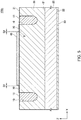
- a gap G2 may exist between the outer peripheral edge of the semiconductor layer 70 and the inner peripheral edge of the outer peripheral trench 10 as in a Schottky barrier diode 100d according to a fourth modification ( FIG. 6 ).
- the electric field concentrating on the outer peripheral edge of the semiconductor layer 70 becomes stronger as the gap G2 is larger, so that the gap G2 should preferably be made as small as possible.
- the semiconductor layer 70 need not be a completely continuous film, but a slit or a cut may be formed in the semiconductor layer 70 so as to partially expose the drift layer 30 therethrough as in a Schottky barrier diode 100e according to a fifth modification ( FIG. 7 ).
- a slit or a cut may be formed in the semiconductor layer 70 so as to partially expose the drift layer 30 therethrough as in a Schottky barrier diode 100e according to a fifth modification ( FIG. 7 ).
- an electric field concentrates on this portion, so that a gap G3 generated by the slit or cut should preferably be as small as possible.
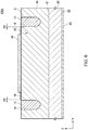
- the outer peripheral trench 10 need not be filled with the embedded layer 11 but may be hollow as in a Schottky barrier diode 100f according to a sixth modification ( FIG. 8 ). In this case as well, the electric field concentrating on the outer peripheral edge of the semiconductor layer 70 is relaxed by the outer peripheral trench 10.
- the surface of the drift layer 30 positioned between the anode electrode 40 and the outer peripheral trench 10 is covered with the semiconductor layer 70 having a conductivity type opposite to that of the drift layer 30.
- the electric field concentrating on the end portion of the anode electrode 40 is relaxed by a depletion layer that extends due to the existence of semiconductor layer 70, and the electric field concentrating on the outer peripheral edge of the semiconductor layer 70 is relaxed by the outer peripheral trench 10. This can prevent dielectric breakdown due to electric field concentration.
- FIG. 9 is a schematic cross-sectional view illustrating the configuration of a Schottky barrier diode 200 according to a second embodiment of the present invention.
- a plurality of center trenches 60 are formed in the drift layer 30.
- the center trenches 60 are all formed at a position overlapping the anode electrode 40 in a plan view.
- the inner wall of each of the center trenches 60 is covered with an insulating film 61 made of HfO 2 or the like.
- the conductive material filled in the center trench 60 may be the same as that of the anode electrode 40 or may be a highly doped polycrystalline Si or a metal material such as Ni or Au.
- the plurality of center trenches 60 are formed in the drift layer 30, so that the anode electrode 40 may be made of a material having a low work function, such as molybdenum (Mo) or copper (Cu). Further, in the present embodiment, the dopant concentration of the drift layer 30 can be increased up to about 5 ⁇ 10 16 cm -3 .
- Other configurations are basically the same as those of the Schottky barrier diode 100 according to the first embodiment, so the same reference numerals are given to the same elements, and overlapping description will be omitted.
- a part of the drift layer 30 positioned between the adjacent center trenches 60 constitutes a mesa region.
- the mesa region becomes a depletion layer when a backward voltage is applied between the anode electrode 40 and the cathode electrode 50, so that a channel region of the drift layer 30 is pinched off.
- a leak current upon application of the backward voltage is significantly reduced.
- the Schottky barrier diode having such a structure, an electric field concentrates on the bottom portion of a center trench 60a positioned at the end portion, making it more susceptible to dielectric breakdown at this portion.
- the surface of the drift layer 30 is covered with the semiconductor layer 70 and the outer peripheral trench 10 is formed at the outer periphery of the center trenches 60 so as to surround the center trenches 60, and hence the electric field concentrating on the center trench 60a at the end portion is relaxed.
- the Schottky barrier diode 200 according to the present embodiment has an effect that can reduce a leak current upon application of a backward voltage, in addition to the effect obtained by the Schottky barrier diode 100 according to the first embodiment.
- the outer peripheral trench 10 and the center trench 60 have the same depth, and thus, they can be formed in the same process.
- the inside of the center trench 60 may be filled with a semiconductor material of an opposite conductivity type (p-type, in the present embodiment) without the use of the insulating film 61.
- Example 1 A simulation model of Example 1 having the same structure as that of the Schottky barrier diode 200 illustrated in FIG. 9 was assumed, and electric field strength was simulated with a backward voltage applied between the anode electrode 40 and the cathode electrode 50.
- the material of the anode electrode 40 was Mo
- the cathode electrode 50 was a laminated film of Ti and Au.
- the dopant concentration of the semiconductor substrate 20 was set to 1 ⁇ 10 18 cm -3
- the dopant concentration of the drift layer 30 was to 5 ⁇ 10 16 cm -3 .
- the thickness of the drift layer 30 was set to 7 ⁇ m.
- the outer peripheral trench 10 was hollow.
- the depth and width of the center trench 60 were set to 3 ⁇ m and 1 ⁇ m, respectively, the mesa width of the mesa region was set to 2 ⁇ m, and the insulating film 61 formed on the inner wall of the center trench 60 was an HfO 2 film having a thickness of 50 nm.
- the semiconductor layer 70 was NiO having an acceptor concentration of 1 ⁇ 10 19 cm -3 and the thickness thereof was set to 100 nm.
- the width a of the semiconductor layer 70 and the width b and depth c of the outer peripheral trench 10 were set to 10 ⁇ m, 10 ⁇ m, and 3 ⁇ m, respectively.
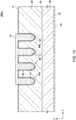
- a simulation model of Comparative Example having the same structure as a Schottky barrier diode 200a illustrated in FIG. 10 was assumed, and electric field strength was simulated with a backward voltage applied between the anode electrode 40 and the cathode electrode 50.
- the Schottky barrier diode 200a illustrated in FIG. 10 differs from the Schottky barrier diode 200 illustrated in FIG. 9 in that the semiconductor layer 70 and outer peripheral trench 10 are removed.
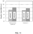
- FIG. 11 illustrates the strength of the electric field applied to areas C and D illustrated in FIGS. 9 and 10 .
- the area C is an area immediately below the center trench 60 positioned at a location other than the end portion
- the area D is an area immediately below the center trench 60a positioned at the end portion.
- the strength of the electric field applied to the area C was 6.5 MV/cm in the simulation model of Example 1 and 6.8 MV/cm in the simulation model of Comparative Example.
- the strength of the electric field applied to the area D was 7.7 MV/cm in the simulation model of Example 1 and 8.1 MV/cm in the simulation model of Comparative Example.
- the electric field strength exceeds about 8 MV/cm, which is the withstand voltage of gallium oxide, in the simulation model of Comparative Example, while it does not exceed about 8 MV/cm in the simulation model of Example 1.
- Example 2 having the same configuration as the simulation model of Example 1 was assumed, and electric field strength was simulated with a backward voltage applied between the anode electrode 40 and the cathode electrode 50 while the width a of the semiconductor layer 70, i.e., the distance between the anode electrode 40 and the outer peripheral trench 10 was variously changed.
- the width b and depth c of the outer peripheral trench 10 were set to 10 ⁇ m and 3 ⁇ m, respectively.
- FIG. 12 is a graph illustrating the simulation result of Example 2.
- the values in the graph of FIG. 12 denote the strength of the electric field applied to a part of the drift layer 30 that covers the outer peripheral edge of the semiconductor layer 70, i.e., an area A in FIG. 9 .
- the strength of the electric field applied to the area A hardly changes even with a change in the width a of the semiconductor layer 70 and is 4.1 MV/cm.
- Example 3 A simulation model of Example 3 having the same configuration as the simulation model of Example 1 was assumed, and electric field strength was simulated with a backward voltage applied between the anode electrode 40 and the cathode electrode 50 while the width b of the outer peripheral trench 10 was variously changed.
- the width a of the semiconductor layer 70 and the depth c of the outer peripheral trench 10 were set to 10 ⁇ m and 3 ⁇ m, respectively.
- FIG. 13 is a graph illustrating the simulation result of Example 3.
- the values in the graph of FIG. 13 also denote the strength of the electric field applied to the area A in FIG. 9 .
- the strength of the electric field applied to the area A hardly changes even with a change in the width b of the outer peripheral trench 10 as long as the width b of the outer peripheral trench 10 is 5 ⁇ m or more and is 4.1 MV/cm.
- the width b of the outer peripheral trench 10 is 1 ⁇ m, the strength of the electric field applied to the area A is 4.7 MV/cm.
- the width b of the outer peripheral trench 10 is preferably 5 ⁇ m or more.
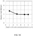
- Example 4 having the same configuration as the simulation model of Example 1 was assumed, and electric field strength was simulated with a backward voltage applied between the anode electrode 40 and the cathode electrode 50 while the depth c of the outer peripheral trench 10 was variously changed.
- the width a of the semiconductor layer 70 and the width b of the outer peripheral trench 10 were set to 10 ⁇ m and 10 ⁇ m, respectively.
- FIG. 14 is a graph illustrating the simulation result of Example 4.
- the values in the graph of FIG. 14 also denote the strength of the electric field applied to the area A in FIG. 9 .
- the strength of the electric field applied to the area A hardly changes even with a change in the depth c of the outer peripheral trench 10 as long as the depth c of the outer peripheral trench 10 is 3 ⁇ m or more and is 3.9 MV/cm to 4.1 MV/cm.
- the depth c of the outer peripheral trench 10 is 1 ⁇ m
- the strength of the electric field applied to the area A is 5.5 MV/cm.
- the width b of the outer peripheral trench 10 is preferably equal to or more than the depth of the center trench 60 (in this example, 3 ⁇ m or more).
- Example 5 A simulation model of Example 5 having the same configuration as the simulation model of Example 1 was assumed, and electric field strength was simulated with a backward voltage applied between the anode electrode 40 and the cathode electrode 50 while the gap G1 illustrated in FIG. 5 was variously changed.
- the width a of the semiconductor layer 70 and the width b and depth of the outer peripheral trench 10 were set to 30 ⁇ m, 10 ⁇ m, and 3 ⁇ m, respectively.
- FIGS. 15 and 16 are each a graph illustrating the simulation result of Example 5.
- the values in the graph of FIG. 15 denote the strength of the electric field applied to an area B in FIG. 5
- the values in the graph of FIG. 16 denote the strength of the electric field applied to the areas C and D in FIG. 9 .
- the area B is an area immediately below the gap Gl
- the area C is an area immediately below the center trench 60 positioned at a location other than the end portion
- the area D is an area immediately below the center trench 60a positioned at the end portion.
- the electric field applied to the area B becomes stronger as the gap G1 increases.
- the electric field strength is 6.8 MV/cm
- the electric field strength is 8.7 MV/cm
- the electric field applied to the area D becomes stronger as the gap G1 is larger.
- the gap G1 is 4 ⁇ m
- the electric field strength is 7.9 MV/cm
- the gap G1 is 5 ⁇ m
- the electric field strength is 8.0 MV/cm.
- the gap G1 is preferably 4 ⁇ m or less.
- Example 6 A simulation model of Example 6 having the same configuration as the simulation model of Example 1 was assumed, and electric field strength was simulated with a backward voltage applied between the anode electrode 40 and the cathode electrode 50 while the gap G2 illustrated in FIG. 6 was variously changed.
- the width a of the semiconductor layer 70 and the width b and depth of the outer peripheral trench 10 were set to 30 ⁇ m, 10 ⁇ m, and 3 ⁇ m, respectively.
- FIG. 17 is a graph illustrating the simulation result of Example 6.
- the values in the graph of FIG. 17 denote the strength of the electric field applied to an area E in FIG. 6 .
- the area E is an area immediately below the gap G2.
- the electric field applied to the area E becomes stronger as the gap G2 is larger.
- the gap G2 is 2 ⁇ m, the electric field strength is 7.9 MV/cm, and when the gap G2 is 3 ⁇ m, the electric field strength is 9.4 MV/cm.
- the gap G2 is preferably 2 ⁇ m or less.
- Example 7 A simulation model of Example 7 having the same configuration as the simulation model of Example 1 was assumed, and electric field strength was simulated with a backward voltage applied between the anode electrode 40 and the cathode electrode 50 while a gap G3 illustrated in FIG. 7 was variously changed.
- the width a of the semiconductor layer 70 and the width b and depth of the outer peripheral trench 10 were set to 30 ⁇ m, 10 ⁇ m, and 3 ⁇ m, respectively.
- FIG. 18 is a graph illustrating the simulation result of Example 7.
- the values in the graph of FIG. 18 denote the strength of the electric field applied to an area F in FIG. 7 .
- the area F is an area immediately below the gap G3.
- the electric field applied to the area F becomes stronger as the gap G3 is larger.
- the gap G3 is 3 ⁇ m, the electric field strength is 7.9 MV/cm, and when the gap G3 is 5 ⁇ m, the electric field strength is 10.1 MV/cm.
- the gap G3 is preferably 3 ⁇ m or less.
- Example 8 having the same configuration as that of the simulation model of Example 1 was assumed, and electric field strength was simulated with a backward voltage applied between the anode electrode 40 and the cathode electrode 50 while the material of the embedded layer 11 in the outer peripheral trench 10 was variously changed.
- the width a of the semiconductor layer 70 and the width b and depth of the outer peripheral trench 10 were set to 10 ⁇ m, 10 ⁇ m, and 3 ⁇ m, respectively.
- FIG. 19 is a graph illustrating the simulation result of Example 8.
- the values in the graph of FIG. 19 denote the maximum values of the electric field strength at a part of the drift layer 30 that is covered with the semiconductor layer 70.
- the electric field applied to the part covered with the semiconductor layer 70 is 4.1 MV/cm when the outer peripheral trench 10 is hollow, 5.8 MV/cm when the embedded layer 11 is made of SiO 2 , 3.6 MV when the embedded layer 11 is made of NiO, and 34.7 MV/cm when the embedded layer 11 is made of Al.
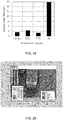
- the electric field is widely dispersed as illustrated in FIG. 20 .
- the strength of the electric field applied to the area A significantly decreases (1 MV/cm or less).
Landscapes
- Electrodes Of Semiconductors (AREA)
Abstract
Description
- The present invention relates to a Schottky barrier diode and, more particularly, to a Schottky barrier diode using gallium oxide.
- A Schottky barrier diode is a rectifying element utilizing a Schottky barrier generated due to bonding between metal and a semiconductor and is lower in forward voltage and higher in switching speed than a normal diode having a PN junction. Thus, the Schottky barrier diode is sometimes utilized as a switching element for a power device.
- When the Schottky barrier diode is utilized as a switching element for a power device, it is necessary to ensure a sufficient backward withstand voltage, so that, silicon carbide (SiC) , gallium nitride (GaN), or gallium oxide (Ga2O3) having a larger band gap is sometimes used in place of silicon (Si). Among them, gallium oxide has a very large band gap (4.8 eV to 4.9 eV) and a large breakdown field (7 MV/cm to 8 MV/cm) , so that a Schottky barrier diode using gallium oxide is very promising as the switching element for a power device. An example of the Schottky barrier diode using gallium oxide is described in
Patent Documents 1 to 3. -
Patent Document 1 discloses a Schottky barrier diode having a field plate structure. A Schottky barrier diode described inPatent Document 2 has a structure in which a plurality of trenches are provided so as to overlap an anode electrode in a plan view, and the inner wall of each of the plurality of trenches is covered with an insulating film. With this structure, when a backward voltage is applied, a mesa region positioned between adjacent trenches becomes a depletion layer, so that a channel region of a drift layer is pinched off. Thus, a leak current upon application of the backward voltage can be significantly reduced. - Further, in a Schottky barrier diode described in
Patent Document 3, a p-type oxide semiconductor layer that covers a drift layer through a nitride layer is provided to form a depletion layer in the drift layer to thereby increase a withstand voltage upon application of a backward voltage. -
- [Patent Document 1]
JP 2017-045969A - [Patent Document 2]
JP 2017-199869A - [Patent Document 3]
International Patent Publication WO 2018/020849 - However, in the Schottky barrier diodes described in
Patent Documents Patent Document 2, an electric field concentrates also on the edge part of the trench positioned at the end portion, which may cause dielectric breakdown at this portion. - In the Schottky barrier diode described in
Patent Document 3, an electric field is relaxed by covering the surface of the drift layer with the p-type oxide semiconductor layer; however, the electric field concentrates on the drift layer at a part thereof that overlaps the end portion of the p-type oxide semiconductor layer, which may cause dielectric breakdown at this portion. - It is therefore an object of the present invention to provide a Schottky barrier diode using gallium oxide, which is less liable to cause dielectric breakdown due to concentration of an electric field.
- A Schottky barrier diode according to the present invention includes: a semiconductor substrate made of gallium oxide; a drift layer made of gallium oxide and provided on the semiconductor substrate; an anode electrode brought into Schottky contact with the drift layer; and a cathode electrode brought into ohmic contact with the semiconductor substrate. The drift layer has an outer peripheral trench surrounding the anode electrode in a plan view. The surface of the drift layer positioned between the anode electrode and the outer peripheral trench is covered with a semiconductor layer having a conductivity type opposite to that of the drift layer.
- According to the present invention, the surface of the drift layer is covered with a semiconductor layer having an opposite conductivity type, so that when a backward voltage is applied, a depletion layer extends around in a part of the drift layer that is covered with the opposite conductivity type semiconductor layer. This relaxes concentration of an electric field on the corner portion of the anode electrode. In addition, the electric field concentrating on the end portion of the semiconductor layer is dispersed by the outer peripheral trench, alleviating electric field concentration on a part of the drift layer that overlaps the end portion of the semiconductor layer. Thus, there can be provided a Schottky barrier diode which is less liable to cause dielectric breakdown due to a backward voltage.
- In the present invention, the semiconductor layer may be made of an oxide semiconductor material. This can prevent a change in characteristics of the semiconductor layer due to oxidation.
- In the present invention, the anode electrode and the semiconductor layer may overlap each other. This can relax electric field concentration more effectively at the corner portion of the anode electrode.
- In the present invention, the outer peripheral trench may be filled with an insulating material or a semiconductor material having a conductivity type opposite to that of the drift layer. In the former case, an electric force line extending in the drift layer can be blocked by the insulating material embedded in the outer peripheral trench, and in the latter case, there can be formed a depletion layer extending from the semiconductor material embedded in the outer peripheral trench to the drift layer.
- In the present invention, the drift layer may further have a plurality of center trenches formed at a position overlapping the anode electrode in a plan view. In this case, the inner wall of each of the plurality of center trenches may be covered with an insulating film. With this configuration, a mesa region positioned between the adjacent center trenches becomes a depletion layer upon application of a backward voltage, so that a channel region of the drift layer is pinched off. Thus, a leak current upon application of the backward voltage can be significantly reduced.
- As described above, according to the present invention, there can be provided a Schottky barrier diode using gallium oxide, which is less liable to cause dielectric breakdown due to concentration of an electric field.
-
-
FIG. 1 is a schematic top view illustrating the configuration of a Schottkybarrier diode 100 according to a first embodiment of the present invention. -
FIG. 2 is a schematic cross-sectional view taken along line A-A inFIG. 1 . -
FIG. 3 is a schematic cross-sectional view illustrating the configuration of a Schottkybarrier diode 100a according to a first modification of the first embodiment. -
FIG. 4 is a schematic cross-sectional view illustrating the configuration of a Schottkybarrier diode 100b according to a second modification of the first embodiment. -
FIG. 5 is a schematic cross-sectional view illustrating the configuration of a Schottkybarrier diode 100c according to a third modification of the first embodiment. -
FIG. 6 is a schematic cross-sectional view illustrating the configuration of a Schottkybarrier diode 100d according to a fourth modification of the first embodiment. -
FIG. 7 is a schematic cross-sectional view illustrating the configuration of a Schottkybarrier diode 100e according to a fifth modification of the first embodiment. -
FIG. 8 is a schematic cross-sectional view illustrating the configuration of a Schottkybarrier diode 100f according to a sixth modification of the first embodiment. -
FIG. 9 is a schematic cross-sectional view illustrating the configuration of a Schottkybarrier diode 200 according to a second embodiment of the present invention. -
FIG. 10 is a schematic cross-sectional view illustrating the configuration of aSchottky barrier diode 200a according to a Comparative Example. -
FIG. 11 is a graph indicating a simulation result of an Example 1. -
FIG. 12 is a graph indicating a simulation result of an Example 2. -
FIG. 13 is a graph indicating a simulation result of an Example 3. -
FIG. 14 is a graph indicating a simulation result of an Example 4. -
FIG. 15 is a graph indicating a simulation result of an Example 5. -
FIG. 16 is a graph indicating a simulation result of an Example 5. -
FIG. 17 is a graph indicating a simulation result of an Example 6. -
FIG. 18 is a graph indicating a simulation result of an Example 7. -
FIG. 19 is a graph indicating a simulation result of an Example 8. -
FIG. 20 is a diagram indicating a simulation result of an Example 8. - Preferred embodiments of the present invention will be explained below in detail with reference to the accompanying drawings.
-
FIG. 1 is a schematic top view illustrating the configuration of aSchottky barrier diode 100 according to a first embodiment of the present invention.FIG. 2 is a schematic cross-sectional view taken along line A-A inFIG. 1 . - As illustrated in
FIGS. 1 and2 , theSchottky barrier diode 100 according to the present embodiment includes asemiconductor substrate 20 and adrift layer 30, both of which are made of gallium oxide (β-Ga2O3) . Thesemiconductor substrate 20 and thedrift layer 30 are each introduced with silicon (Si) or tin (Sn) as an n-type dopant. The concentration of the dopant is higher in thesemiconductor substrate 20 than in thedrift layer 30, whereby thesemiconductor substrate 20 and thedrift layer 30 function as an n+ layer and an n- layer, respectively. - The
semiconductor substrate 20 is obtained by cutting a bulk crystal formed using a melt-growing method, and the thickness (height in the Z-direction) thereof is about 250 µm. Although there is no particular restriction on the planar size of thesemiconductor substrate 20, the planar size is generally selected in accordance with the amount of current flowing in the element and, when the maximum amount of forward current is about 20 A, the widths in the X- and Y-directions may be set to about 2.4 mm. - The
semiconductor substrate 20 has anupper surface 21 positioned on the upper surface side and aback surface 22 positioned on the lower surface side, in a mounted state. Thedrift layer 30 is formed on the entireupper surface 21. Thedrift layer 30 is a thin film obtained by epitaxially growing gallium oxide on theupper surface 21 of thesemiconductor substrate 20 using a reactive sputtering method, a PLD method, an MBE method, an MOCVD method, or an HVPE method. Although there is no particular restriction on the film thickness of thedrift layer 30, the film thickness is generally selected in accordance with the backward withstand voltage of the element and may be set to, e.g., about 7 µm in order to ensure a withstand voltage of about 600 V. - An
anode electrode 40 is formed on anupper surface 31 of thedrift layer 30 so as to be brought into Schottky contact with thedrift layer 30. Theanode electrode 40 is formed of metal such as platinum (Pt), palladium (Pd), gold (Au), nickel (Ni), or the like. Theanode electrode 40 may have a multilayer structure of different metal films such as Pt/Au, Pt/Al, Pd/Au, Pd/Al, Pt/Ti/Au, or Pd/Ti/Au. On the other hand, acathode electrode 50 is formed on theback surface 22 of thesemiconductor substrate 20 so as to be brought into ohmic contact with thesemiconductor substrate 20. Thecathode electrode 50 is formed of metal such as titanium (Ti). Thecathode electrode 50 may have a multilayer structure of different metal films such as Ti/Au or Ti/Al. - Further, the
drift layer 30 has formed therein an outerperipheral trench 10 at a position not overlapping theanode electrode 40 in a plan view (as viewed in the Z-direction) so as to surround theanode electrode 40. The outerperipheral trench 10 can be formed by etching thedrift layer 30 from theupper surface 31 side. - The outer
peripheral trench 10 is filled with an embeddedlayer 11. The embeddedlayer 11 may be an insulating material such as SiO2 or a semiconductor material having a conductivity type opposite to that of thedrift layer 30. That is, when the semiconductor material is used as the material of the embeddedlayer 11, a p-type semiconductor material needs to be selected since the conductivity type of thedrift layer 30 is an n-type. The semiconductor material filled in the outerperipheral trench 10 may be in a floating state. - Further, a part of the surface of the
drift layer 30 positioned between theanode electrode 40 and the outerperipheral trench 10 is covered with asemiconductor layer 70 having a conductivity type opposite to that of thedrift layer 30. Thedrift layer 30 and thesemiconductor layer 70 may directly contact each other, or may contact each other through an insulating film or the like. Since the conductivity type of thedrift layer 30 is an n-type, thesemiconductor layer 70 needs to be formed of a p-type semiconductor material. Examples of the p-type semiconductor material include Si, GaAs, SiC, Ge, ZnSe, CdS, InP, SiGe, and a p-type oxide semiconductor such as NiO, Cu2O, or Ag2O. The p-type semiconductor material has an advantage of being free from oxidation. In particular, NiO is a special material that exhibits only a p-type conductivity and is most preferable in terms of quality stabilization. Further, NiO has a band gap as large as 3.7 eV and is thus desirable as a material taking advantage of high withstand voltage of gallium oxide. Further, to control acceptor concentration, Li or La may be added as a dopant in a ratio of about 0.2 mol% to 1.0 mol% to NiO (99.9%). The acceptor concentration is preferably equal to or higher than 5 × 1017 cm-3 and more preferably equal to or higher than 5 × 1018 cm-3 in terms of production stability. This is because a low acceptor concentration may cause depletion of thesemiconductor layer 70, which may fail to provide a desired function. Thus, a higher acceptor concentration is more preferable. However, when the acceptor concentration exceeds 1 × 1022 cm-3, film characteristics may deteriorate, so that the acceptor concentration is preferably equal to or lower than about 5 × 1021 cm-3. Thesemiconductor layer 70 may be in a floating state, or may contact theanode electrode 40 or the embeddedlayer 11 embedded in the outerperipheral trench 10. The surface of thesemiconductor layer 70 is preferably covered with a passivation film of SiO2 or the like. - When in a fully amorphous state, the p-type oxide constituting the
semiconductor layer 70 is unintentionally crystallized in a heating process during device production, which may make the characteristics thereof unstable. Considering this, at the time when the p-type oxide is formed on thedrift layer 30, about 50% by volume thereof may be crystallized, for example. This can reduce the influence of crystallization in a heat process during device production. - Since the
semiconductor layer 70 has a conductivity type opposite to that of thedrift layer 30, a depletion layer extends around a part of thedrift layer 30 that is covered with thesemiconductor layer 70 due to a potential difference. Thus, when a backward voltage is applied between theanode electrode 40 and thecathode electrode 50, an electric field concentrating on the end portion of theanode electrode 40 is relaxed. The electric field concentrating on the end portion of theanode electrode 40 is relaxed more effectively as a gap between theanode electrode 40 and thesemiconductor layer 70 is smaller, so that theanode electrode 40 and thesemiconductor layer 70 preferably contact each other. When it is difficult to make the outer peripheral edge of theanode electrode 40 and the inner peripheral edge of thesemiconductor layer 70 coincide with each other, a part of thesemiconductor layer 70 may be formed on theanode electrode 40 so as to cover the outer peripheral edge of theanode electrode 40 as in aSchottky barrier diode 100a according to a first modification (FIG. 3 ). Alternatively, a part of theanode electrode 40 may be formed on thesemiconductor layer 70 so as to cover the inner peripheral edge of thesemiconductor layer 70 as in aSchottky barrier diode 100b according to a second modification (FIG. 4 ). With the above configurations, an overlap occurs between theanode electrode 40 and thesemiconductor layer 70, allowing theanode electrode 40 andsemiconductor layer 70 to reliably contact each other. - However, in the present invention, it is not essential to make the
anode electrode 40 and thesemiconductor layer 70 contact each other, but a gap G1 may exist between the outer peripheral edge of theanode electrode 40 and the inner peripheral edge of thesemiconductor layer 70 as in aSchottky barrier diode 100c according to a third modification (FIG. 5 ). The electric field concentrating on the end portion of theanode electrode 40 becomes stronger as the gap G1 is larger, so that the gap G1 should preferably be as small as possible. - As described above, the electric field concentrating on the end portion of the
anode electrode 40 is relaxed by providing thesemiconductor layer 70. In this case, the electric field concentrates on the outer peripheral edge of thesemiconductor layer 70, which, however, is relaxed by the outerperipheral trench 10. Thus, in the present embodiment, the electric field concentrating on the end portion of theanode electrode 40 is relaxed by thesemiconductor layer 70, and the electric field concentrating on the outer peripheral edge of thesemiconductor layer 70 is relaxed by the outerperipheral trench 10, thereby making it possible to prevent dielectric breakdown upon application of a backward voltage. - The electric field concentrating on the outer peripheral edge of the
semiconductor layer 70 is relaxed more effectively as a gap between the outer peripheral edge of thesemiconductor layer 70 and the inner peripheral edge of the outerperipheral trench 10 is smaller, so that it is preferable that the outer peripheral edge of thesemiconductor layer 70 and the inner peripheral edge of the outerperipheral trench 10 coincide with each other. When the embeddedlayer 11 in the outerperipheral trench 10 is made of the same material as that of thesemiconductor layer 70, thesemiconductor layer 70 and embedded layer 11may be continuously formed. However, in the present invention, it is not essential to make the outer peripheral edge of thesemiconductor layer 70 and the inner peripheral edge of the outerperipheral trench 10 coincide with each other, but a gap G2 may exist between the outer peripheral edge of thesemiconductor layer 70 and the inner peripheral edge of the outerperipheral trench 10 as in aSchottky barrier diode 100d according to a fourth modification (FIG. 6 ). The electric field concentrating on the outer peripheral edge of thesemiconductor layer 70 becomes stronger as the gap G2 is larger, so that the gap G2 should preferably be made as small as possible. - The
semiconductor layer 70 need not be a completely continuous film, but a slit or a cut may be formed in thesemiconductor layer 70 so as to partially expose thedrift layer 30 therethrough as in aSchottky barrier diode 100e according to a fifth modification (FIG. 7 ). However, when the slit or cut exists in thesemiconductor layer 70, an electric field concentrates on this portion, so that a gap G3 generated by the slit or cut should preferably be as small as possible. - Further, the outer
peripheral trench 10 need not be filled with the embeddedlayer 11 but may be hollow as in aSchottky barrier diode 100f according to a sixth modification (FIG. 8 ). In this case as well, the electric field concentrating on the outer peripheral edge of thesemiconductor layer 70 is relaxed by the outerperipheral trench 10. - As described above, in the
Schottky barrier diode 100 according to the present embodiment, the surface of thedrift layer 30 positioned between theanode electrode 40 and the outerperipheral trench 10 is covered with thesemiconductor layer 70 having a conductivity type opposite to that of thedrift layer 30. Thus, the electric field concentrating on the end portion of theanode electrode 40 is relaxed by a depletion layer that extends due to the existence ofsemiconductor layer 70, and the electric field concentrating on the outer peripheral edge of thesemiconductor layer 70 is relaxed by the outerperipheral trench 10. This can prevent dielectric breakdown due to electric field concentration. -
FIG. 9 is a schematic cross-sectional view illustrating the configuration of aSchottky barrier diode 200 according to a second embodiment of the present invention. - As illustrated in
FIG. 9 , in theSchottky barrier diode 200 according to the second embodiment, a plurality ofcenter trenches 60 are formed in thedrift layer 30. Thecenter trenches 60 are all formed at a position overlapping theanode electrode 40 in a plan view. The inner wall of each of thecenter trenches 60 is covered with an insulating film 61 made of HfO2 or the like. The conductive material filled in thecenter trench 60 may be the same as that of theanode electrode 40 or may be a highly doped polycrystalline Si or a metal material such as Ni or Au. In the present embodiment, the plurality ofcenter trenches 60 are formed in thedrift layer 30, so that theanode electrode 40 may be made of a material having a low work function, such as molybdenum (Mo) or copper (Cu). Further, in the present embodiment, the dopant concentration of thedrift layer 30 can be increased up to about 5 × 1016 cm-3. Other configurations are basically the same as those of theSchottky barrier diode 100 according to the first embodiment, so the same reference numerals are given to the same elements, and overlapping description will be omitted. - A part of the
drift layer 30 positioned between theadjacent center trenches 60 constitutes a mesa region. The mesa region becomes a depletion layer when a backward voltage is applied between theanode electrode 40 and thecathode electrode 50, so that a channel region of thedrift layer 30 is pinched off. Thus, a leak current upon application of the backward voltage is significantly reduced. - In the Schottky barrier diode having such a structure, an electric field concentrates on the bottom portion of a
center trench 60a positioned at the end portion, making it more susceptible to dielectric breakdown at this portion. However, in theSchottky barrier diode 200 according to the present embodiment, the surface of thedrift layer 30 is covered with thesemiconductor layer 70 and the outerperipheral trench 10 is formed at the outer periphery of thecenter trenches 60 so as to surround thecenter trenches 60, and hence the electric field concentrating on thecenter trench 60a at the end portion is relaxed. - As described above, the
Schottky barrier diode 200 according to the present embodiment has an effect that can reduce a leak current upon application of a backward voltage, in addition to the effect obtained by theSchottky barrier diode 100 according to the first embodiment. Further, in the present embodiment, the outerperipheral trench 10 and thecenter trench 60 have the same depth, and thus, they can be formed in the same process. - Further, although the inner wall of the
center trench 60 is covered with the insulating film 61, and the inside thereof is filled with the same material as theanode electrode 40 in the present embodiment, the inside of thecenter trench 60 may be filled with a semiconductor material of an opposite conductivity type (p-type, in the present embodiment) without the use of the insulating film 61. - While the preferred embodiments of the present invention have been described, the present invention is not limited to the above embodiments, and various modifications may be made within the scope of the present invention, and all such modifications are included in the present invention.
- A simulation model of Example 1 having the same structure as that of the
Schottky barrier diode 200 illustrated inFIG. 9 was assumed, and electric field strength was simulated with a backward voltage applied between theanode electrode 40 and thecathode electrode 50. The material of theanode electrode 40 was Mo, and thecathode electrode 50 was a laminated film of Ti and Au. The dopant concentration of thesemiconductor substrate 20 was set to 1 × 1018 cm-3, and the dopant concentration of thedrift layer 30 was to 5 × 1016 cm-3. The thickness of thedrift layer 30 was set to 7 µm. The outerperipheral trench 10 was hollow. The depth and width of thecenter trench 60 were set to 3 µm and 1 µm, respectively, the mesa width of the mesa region was set to 2 µm, and the insulating film 61 formed on the inner wall of thecenter trench 60 was an HfO2 film having a thickness of 50 nm. Thesemiconductor layer 70 was NiO having an acceptor concentration of 1 × 1019 cm-3 and the thickness thereof was set to 100 nm. The width a of thesemiconductor layer 70 and the width b and depth c of the outerperipheral trench 10 were set to 10 µm, 10 µm, and 3 µm, respectively. - For comparison, a simulation model of Comparative Example having the same structure as a
Schottky barrier diode 200a illustrated inFIG. 10 was assumed, and electric field strength was simulated with a backward voltage applied between theanode electrode 40 and thecathode electrode 50. TheSchottky barrier diode 200a illustrated inFIG. 10 differs from theSchottky barrier diode 200 illustrated inFIG. 9 in that thesemiconductor layer 70 and outerperipheral trench 10 are removed. -
FIG. 11 illustrates the strength of the electric field applied to areas C and D illustrated inFIGS. 9 and10 . The area C is an area immediately below thecenter trench 60 positioned at a location other than the end portion, and the area D is an area immediately below thecenter trench 60a positioned at the end portion. - As illustrated in
FIG. 11 , the strength of the electric field applied to the area C was 6.5 MV/cm in the simulation model of Example 1 and 6.8 MV/cm in the simulation model of Comparative Example. On the other hand, the strength of the electric field applied to the area D was 7.7 MV/cm in the simulation model of Example 1 and 8.1 MV/cm in the simulation model of Comparative Example. Thus, the electric field strength exceeds about 8 MV/cm, which is the withstand voltage of gallium oxide, in the simulation model of Comparative Example, while it does not exceed about 8 MV/cm in the simulation model of Example 1. - A simulation model of Example 2 having the same configuration as the simulation model of Example 1 was assumed, and electric field strength was simulated with a backward voltage applied between the
anode electrode 40 and thecathode electrode 50 while the width a of thesemiconductor layer 70, i.e., the distance between theanode electrode 40 and the outerperipheral trench 10 was variously changed. The width b and depth c of the outerperipheral trench 10 were set to 10 µm and 3 µm, respectively. -
FIG. 12 is a graph illustrating the simulation result of Example 2. The values in the graph ofFIG. 12 denote the strength of the electric field applied to a part of thedrift layer 30 that covers the outer peripheral edge of thesemiconductor layer 70, i.e., an area A inFIG. 9 . As illustrated in the graph ofFIG. 12 , the strength of the electric field applied to the area A hardly changes even with a change in the width a of thesemiconductor layer 70 and is 4.1 MV/cm. - A simulation model of Example 3 having the same configuration as the simulation model of Example 1 was assumed, and electric field strength was simulated with a backward voltage applied between the
anode electrode 40 and thecathode electrode 50 while the width b of the outerperipheral trench 10 was variously changed. The width a of thesemiconductor layer 70 and the depth c of the outerperipheral trench 10 were set to 10 µm and 3 µm, respectively. -
FIG. 13 is a graph illustrating the simulation result of Example 3. The values in the graph ofFIG. 13 also denote the strength of the electric field applied to the area A inFIG. 9 . As illustrated in the graph ofFIG. 13 , the strength of the electric field applied to the area A hardly changes even with a change in the width b of the outerperipheral trench 10 as long as the width b of the outerperipheral trench 10 is 5 µm or more and is 4.1 MV/cm. On the other hand, when the width b of the outerperipheral trench 10 is 1 µm, the strength of the electric field applied to the area A is 4.7 MV/cm. Thus, the width b of the outerperipheral trench 10 is preferably 5 µm or more. - A simulation model of Example 4 having the same configuration as the simulation model of Example 1 was assumed, and electric field strength was simulated with a backward voltage applied between the
anode electrode 40 and thecathode electrode 50 while the depth c of the outerperipheral trench 10 was variously changed. The width a of thesemiconductor layer 70 and the width b of the outerperipheral trench 10 were set to 10 µm and 10 µm, respectively. -
FIG. 14 is a graph illustrating the simulation result of Example 4. The values in the graph ofFIG. 14 also denote the strength of the electric field applied to the area A inFIG. 9 . As illustrated in the graph ofFIG. 14 , the strength of the electric field applied to the area A hardly changes even with a change in the depth c of the outerperipheral trench 10 as long as the depth c of the outerperipheral trench 10 is 3 µm or more and is 3.9 MV/cm to 4.1 MV/cm. On the other hand, when the depth c of the outerperipheral trench 10 is 1 µm, the strength of the electric field applied to the area A is 5.5 MV/cm. Thus, the width b of the outerperipheral trench 10 is preferably equal to or more than the depth of the center trench 60 (in this example, 3 µm or more). - A simulation model of Example 5 having the same configuration as the simulation model of Example 1 was assumed, and electric field strength was simulated with a backward voltage applied between the
anode electrode 40 and thecathode electrode 50 while the gap G1 illustrated inFIG. 5 was variously changed. The width a of thesemiconductor layer 70 and the width b and depth of the outerperipheral trench 10 were set to 30 µm, 10 µm, and 3 µm, respectively. -
FIGS. 15 and 16 are each a graph illustrating the simulation result of Example 5. The values in the graph ofFIG. 15 denote the strength of the electric field applied to an area B inFIG. 5 , and the values in the graph ofFIG. 16 denote the strength of the electric field applied to the areas C and D inFIG. 9 . The area B is an area immediately below the gap Gl, the area C is an area immediately below thecenter trench 60 positioned at a location other than the end portion, and the area D is an area immediately below thecenter trench 60a positioned at the end portion. As illustrated inFIG. 15 , the electric field applied to the area B becomes stronger as the gap G1 increases. Specifically, when the gap G1 is 4 µm, the electric field strength is 6.8 MV/cm, and when the gap G1 is 5 µm, the electric field strength is 8.7 MV/cm. Similarly, as illustrated inFIG. 16 , the electric field applied to the area D becomes stronger as the gap G1 is larger. Specifically, when the gap G1 is 4 µm, the electric field strength is 7.9 MV/cm, and when the gap G1 is 5 µm, the electric field strength is 8.0 MV/cm. Thus, considering that the withstand voltage of gallium oxide is about 8 MV/cm, the gap G1 is preferably 4 µm or less. - A simulation model of Example 6 having the same configuration as the simulation model of Example 1 was assumed, and electric field strength was simulated with a backward voltage applied between the
anode electrode 40 and thecathode electrode 50 while the gap G2 illustrated inFIG. 6 was variously changed. The width a of thesemiconductor layer 70 and the width b and depth of the outerperipheral trench 10 were set to 30 µm, 10 µm, and 3 µm, respectively. -
FIG. 17 is a graph illustrating the simulation result of Example 6. The values in the graph ofFIG. 17 denote the strength of the electric field applied to an area E inFIG. 6 . The area E is an area immediately below the gap G2. As illustrated inFIG. 17 , the electric field applied to the area E becomes stronger as the gap G2 is larger. Specifically, when the gap G2 is 2 µm, the electric field strength is 7.9 MV/cm, and when the gap G2 is 3 µm, the electric field strength is 9.4 MV/cm. Thus, considering that the withstand voltage of gallium oxide is about 8 MV/cm, the gap G2 is preferably 2 µm or less. - A simulation model of Example 7 having the same configuration as the simulation model of Example 1 was assumed, and electric field strength was simulated with a backward voltage applied between the
anode electrode 40 and thecathode electrode 50 while a gap G3 illustrated inFIG. 7 was variously changed. The width a of thesemiconductor layer 70 and the width b and depth of the outerperipheral trench 10 were set to 30 µm, 10 µm, and 3 µm, respectively. -
FIG. 18 is a graph illustrating the simulation result of Example 7. The values in the graph ofFIG. 18 denote the strength of the electric field applied to an area F inFIG. 7 . The area F is an area immediately below the gap G3. As illustrated inFIG. 18 , the electric field applied to the area F becomes stronger as the gap G3 is larger. Specifically, when the gap G3 is 3 µm, the electric field strength is 7.9 MV/cm, and when the gap G3 is 5 µm, the electric field strength is 10.1 MV/cm. Thus, considering that the withstand voltage of gallium oxide is about 8 MV/cm, the gap G3 is preferably 3 µm or less. - A simulation model of Example 8 having the same configuration as that of the simulation model of Example 1 was assumed, and electric field strength was simulated with a backward voltage applied between the
anode electrode 40 and thecathode electrode 50 while the material of the embeddedlayer 11 in the outerperipheral trench 10 was variously changed. The width a of thesemiconductor layer 70 and the width b and depth of the outerperipheral trench 10 were set to 10 µm, 10 µm, and 3 µm, respectively. -
FIG. 19 is a graph illustrating the simulation result of Example 8. The values in the graph ofFIG. 19 denote the maximum values of the electric field strength at a part of thedrift layer 30 that is covered with thesemiconductor layer 70. As illustrated inFIG. 19 , the electric field applied to the part covered with thesemiconductor layer 70 is 4.1 MV/cm when the outerperipheral trench 10 is hollow, 5.8 MV/cm when the embeddedlayer 11 is made of SiO2, 3.6 MV when the embeddedlayer 11 is made of NiO, and 34.7 MV/cm when the embeddedlayer 11 is made of Al. - When the embedded
layer 11 is made of NiO, the electric field is widely dispersed as illustrated inFIG. 20 . In particular, the strength of the electric field applied to the area A significantly decreases (1 MV/cm or less). -
- 10
- outer peripheral trench
- 11
- embedded layer
- 20
- semiconductor substrate
- 21
- upper surface of semiconductor substrate
- 22
- back surface of semiconductor substrate
- 30
- drift layer
- 31
- upper surface of the drift layer
- 40
- anode electrode
- 50
- cathode electrode
- 60
- center trench
- 60a
- center trench positioned at end portion
- 61
- insulating film
- 70
- semiconductor layer
- 100, 100a-100f, 200, 200a
- Schottky barrier diode
- A-F
- area
- G1-G3
- gap
Claims (6)
- A Schottky barrier diode comprising:a semiconductor substrate made of gallium oxide;a drift layer made of gallium oxide and provided on the semiconductor substrate;an anode electrode brought into Schottky contact with the drift layer; anda cathode electrode brought into ohmic contact with the semiconductor substrate,wherein the drift layer has an outer peripheral trench surrounding the anode electrode in a plan view, andwherein a surface of the drift layer positioned between the anode electrode and the outer peripheral trench is covered with a semiconductor layer having a conductivity type opposite to that of the drift layer.
- The Schottky barrier diode as claimed in claim 1, wherein the semiconductor layer is made of an oxide semiconductor material.
- The Schottky barrier diode as claimed in claim 1 or 2, wherein the anode electrode and the semiconductor layer overlap each other.
- The Schottky barrier diode as claimed in any one of claims 1 to 3, wherein the outer peripheral trench is filled with an insulating material or a semiconductor material having a conductivity type opposite to that of the drift layer.
- The Schottky barrier diode as claimed in any one of claims 1 to 4, wherein the drift layer further has a plurality of center trenches formed at a position overlapping the anode electrode in a plan view.
- The Schottky barrier diode as claimed in claim 5, wherein an inner wall of each of the plurality of center trenches is covered with an insulating film.
Applications Claiming Priority (2)
| Application Number | Priority Date | Filing Date | Title |
|---|---|---|---|
| JP2018199202A JP6966739B2 (en) | 2018-10-23 | 2018-10-23 | Schottky barrier diode |
| PCT/JP2019/039853 WO2020085094A1 (en) | 2018-10-23 | 2019-10-09 | Schottky barrier diode |
Publications (2)
| Publication Number | Publication Date |
|---|---|
| EP3872865A1 true EP3872865A1 (en) | 2021-09-01 |
| EP3872865A4 EP3872865A4 (en) | 2022-07-13 |
Family
ID=70331051
Family Applications (1)
| Application Number | Title | Priority Date | Filing Date |
|---|---|---|---|
| EP19875151.3A Pending EP3872865A4 (en) | 2018-10-23 | 2019-10-09 | SCHOTTKY BARRIER DIODE |
Country Status (5)
| Country | Link |
|---|---|
| US (1) | US11557681B2 (en) |
| EP (1) | EP3872865A4 (en) |
| JP (1) | JP6966739B2 (en) |
| CN (1) | CN112913034B (en) |
| WO (1) | WO2020085094A1 (en) |
Cited By (1)
| Publication number | Priority date | Publication date | Assignee | Title |
|---|---|---|---|---|
| RU2805563C1 (en) * | 2023-03-01 | 2023-10-19 | Общество с ограниченной ответственностью Арсенид-галлиевые актуальные технологии (ООО АГАТ) | High-voltage power diode crystal with schottky barrier and p-n junctions |
Families Citing this family (9)
| Publication number | Priority date | Publication date | Assignee | Title |
|---|---|---|---|---|
| JP7415537B2 (en) * | 2019-12-18 | 2024-01-17 | Tdk株式会社 | schottky barrier diode |
| JPWO2022270525A1 (en) * | 2021-06-25 | 2022-12-29 | ||
| CN113871454A (en) * | 2021-09-28 | 2021-12-31 | 西安电子科技大学芜湖研究院 | Gallium oxide Schottky barrier diode based on silicon dioxide edge termination and preparation method thereof |
| CN114639719A (en) * | 2022-02-28 | 2022-06-17 | 北海惠科半导体科技有限公司 | Trench Schottky diode and preparation method thereof |
| CN117438476A (en) * | 2022-07-14 | 2024-01-23 | 无锡华润上华科技有限公司 | Trench Schottky barrier semiconductor structure and preparation method thereof |
| JP2024047430A (en) * | 2022-09-26 | 2024-04-05 | 株式会社タムラ製作所 | Schottky Barrier Diode |
| TWI905790B (en) * | 2023-09-21 | 2025-11-21 | 日商Tdk股份有限公司 | Semiconductor device |
| TWI901178B (en) * | 2023-09-21 | 2025-10-11 | 日商Tdk股份有限公司 | Semiconductor device |
| WO2025191758A1 (en) * | 2024-03-13 | 2025-09-18 | 三菱電機株式会社 | Semiconductor device, power conversion device, and manufacturing method for semiconductor device |
Family Cites Families (13)
| Publication number | Priority date | Publication date | Assignee | Title |
|---|---|---|---|---|
| JP2005005486A (en) * | 2003-06-12 | 2005-01-06 | Shindengen Electric Mfg Co Ltd | Silicon carbide semiconductor device |
| WO2012098636A1 (en) * | 2011-01-17 | 2012-07-26 | 富士通株式会社 | Semiconductor device and manufacturing method thereof |
| JP5414715B2 (en) * | 2011-03-04 | 2014-02-12 | 株式会社日立製作所 | Nitride semiconductor diode |
| US8741707B2 (en) * | 2011-12-22 | 2014-06-03 | Avogy, Inc. | Method and system for fabricating edge termination structures in GaN materials |
| JP5888214B2 (en) * | 2012-11-30 | 2016-03-16 | 富士電機株式会社 | Nitride-based compound semiconductor device and manufacturing method thereof |
| JP6267108B2 (en) * | 2014-12-22 | 2018-01-24 | トヨタ自動車株式会社 | Schottky barrier diode and manufacturing method thereof |
| JP2017045969A (en) | 2015-08-28 | 2017-03-02 | 株式会社タムラ製作所 | Schottky barrier diode |
| JP6845397B2 (en) * | 2016-04-28 | 2021-03-17 | 株式会社タムラ製作所 | Trench MOS type Schottky diode |
| US10483110B2 (en) * | 2016-07-26 | 2019-11-19 | Mitsubishi Electric Corporation | Semiconductor device and method of manufacturing semiconductor device |
| JP6667712B2 (en) * | 2017-02-14 | 2020-03-18 | 三菱電機株式会社 | Power semiconductor device |
| JP6967238B2 (en) * | 2017-02-28 | 2021-11-17 | 株式会社タムラ製作所 | Schottky barrier diode |
| US10636663B2 (en) | 2017-03-29 | 2020-04-28 | Toyoda Gosei Co., Ltd. | Method of manufacturing semiconductor device including implanting impurities into an implanted region of a semiconductor layer and annealing the implanted region |
| JP7165322B2 (en) * | 2018-03-30 | 2022-11-04 | Tdk株式会社 | schottky barrier diode |
-
2018
- 2018-10-23 JP JP2018199202A patent/JP6966739B2/en active Active
-
2019
- 2019-10-09 WO PCT/JP2019/039853 patent/WO2020085094A1/en not_active Ceased
- 2019-10-09 CN CN201980070323.9A patent/CN112913034B/en active Active
- 2019-10-09 US US17/282,610 patent/US11557681B2/en active Active
- 2019-10-09 EP EP19875151.3A patent/EP3872865A4/en active Pending
Cited By (1)
| Publication number | Priority date | Publication date | Assignee | Title |
|---|---|---|---|---|
| RU2805563C1 (en) * | 2023-03-01 | 2023-10-19 | Общество с ограниченной ответственностью Арсенид-галлиевые актуальные технологии (ООО АГАТ) | High-voltage power diode crystal with schottky barrier and p-n junctions |
Also Published As
| Publication number | Publication date |
|---|---|
| CN112913034B (en) | 2024-02-23 |
| JP2020068259A (en) | 2020-04-30 |
| JP6966739B2 (en) | 2021-11-17 |
| WO2020085094A1 (en) | 2020-04-30 |
| US11557681B2 (en) | 2023-01-17 |
| US20210343879A1 (en) | 2021-11-04 |
| CN112913034A (en) | 2021-06-04 |
| EP3872865A4 (en) | 2022-07-13 |
Similar Documents
| Publication | Publication Date | Title |
|---|---|---|
| US11621357B2 (en) | Schottky barrier diode | |
| US11557681B2 (en) | Schottky barrier diode | |
| US11469334B2 (en) | Schottky barrier diode | |
| US11626522B2 (en) | Schottky barrier diode | |
| US11908955B2 (en) | Schottky barrier diode | |
| US20240313130A1 (en) | Junction barrier schottky diode | |
| US11699766B2 (en) | Schottky barrier diode | |
| US20240313129A1 (en) | Schottky barrier diode | |
| US20260006809A1 (en) | Junction barrier schottky diode | |
| WO2024047965A1 (en) | Schottky barrier diode | |
| US20250015201A1 (en) | Junction barrier schottky diode | |
| US12520510B2 (en) | Schottky barrier diode | |
| US20260013157A1 (en) | Schottky barrier diode | |
| US20250081485A1 (en) | Junction barrier schottky diode |
Legal Events
| Date | Code | Title | Description |
|---|---|---|---|
| STAA | Information on the status of an ep patent application or granted ep patent |
Free format text: STATUS: THE INTERNATIONAL PUBLICATION HAS BEEN MADE |
|
| PUAI | Public reference made under article 153(3) epc to a published international application that has entered the european phase |
Free format text: ORIGINAL CODE: 0009012 |
|
| STAA | Information on the status of an ep patent application or granted ep patent |
Free format text: STATUS: REQUEST FOR EXAMINATION WAS MADE |
|
| 17P | Request for examination filed |
Effective date: 20210518 |
|
| AK | Designated contracting states |
Kind code of ref document: A1 Designated state(s): AL AT BE BG CH CY CZ DE DK EE ES FI FR GB GR HR HU IE IS IT LI LT LU LV MC MK MT NL NO PL PT RO RS SE SI SK SM TR |
|
| DAV | Request for validation of the european patent (deleted) | ||
| DAX | Request for extension of the european patent (deleted) | ||
| A4 | Supplementary search report drawn up and despatched |
Effective date: 20220613 |
|
| RIC1 | Information provided on ipc code assigned before grant |
Ipc: H01L 29/267 20060101ALI20220608BHEP Ipc: H01L 29/24 20060101ALI20220608BHEP Ipc: H01L 29/47 20060101ALI20220608BHEP Ipc: H01L 29/41 20060101ALI20220608BHEP Ipc: H01L 29/06 20060101ALI20220608BHEP Ipc: H01L 29/872 20060101AFI20220608BHEP |
|
| STAA | Information on the status of an ep patent application or granted ep patent |
Free format text: STATUS: EXAMINATION IS IN PROGRESS |
|
| 17Q | First examination report despatched |
Effective date: 20260102 |