EP3866321A1 - Ac-dc converter, dc-dc converter, and ac-ac converter - Google Patents
Ac-dc converter, dc-dc converter, and ac-ac converter Download PDFInfo
- Publication number
- EP3866321A1 EP3866321A1 EP19871651.6A EP19871651A EP3866321A1 EP 3866321 A1 EP3866321 A1 EP 3866321A1 EP 19871651 A EP19871651 A EP 19871651A EP 3866321 A1 EP3866321 A1 EP 3866321A1
- Authority
- EP
- European Patent Office
- Prior art keywords
- voltage
- circuit
- buffer
- current
- converter
- Prior art date
- Legal status (The legal status is an assumption and is not a legal conclusion. Google has not performed a legal analysis and makes no representation as to the accuracy of the status listed.)
- Pending
Links
Images








Classifications
-
- H—ELECTRICITY
- H02—GENERATION; CONVERSION OR DISTRIBUTION OF ELECTRIC POWER
- H02M—APPARATUS FOR CONVERSION BETWEEN AC AND AC, BETWEEN AC AND DC, OR BETWEEN DC AND DC, AND FOR USE WITH MAINS OR SIMILAR POWER SUPPLY SYSTEMS; CONVERSION OF DC OR AC INPUT POWER INTO SURGE OUTPUT POWER; CONTROL OR REGULATION THEREOF
- H02M7/00—Conversion of AC power input into DC power output; Conversion of DC power input into AC power output
- H02M7/02—Conversion of AC power input into DC power output without possibility of reversal
- H02M7/04—Conversion of AC power input into DC power output without possibility of reversal by static converters
- H02M7/06—Conversion of AC power input into DC power output without possibility of reversal by static converters using discharge tubes without control electrode or semiconductor devices without control electrode
-
- H—ELECTRICITY
- H02—GENERATION; CONVERSION OR DISTRIBUTION OF ELECTRIC POWER
- H02M—APPARATUS FOR CONVERSION BETWEEN AC AND AC, BETWEEN AC AND DC, OR BETWEEN DC AND DC, AND FOR USE WITH MAINS OR SIMILAR POWER SUPPLY SYSTEMS; CONVERSION OF DC OR AC INPUT POWER INTO SURGE OUTPUT POWER; CONTROL OR REGULATION THEREOF
- H02M1/00—Details of apparatus for conversion
- H02M1/0067—Converter structures employing plural converter units, other than for parallel operation of the units on a single load
- H02M1/007—Plural converter units in cascade
-
- H—ELECTRICITY
- H02—GENERATION; CONVERSION OR DISTRIBUTION OF ELECTRIC POWER
- H02M—APPARATUS FOR CONVERSION BETWEEN AC AND AC, BETWEEN AC AND DC, OR BETWEEN DC AND DC, AND FOR USE WITH MAINS OR SIMILAR POWER SUPPLY SYSTEMS; CONVERSION OF DC OR AC INPUT POWER INTO SURGE OUTPUT POWER; CONTROL OR REGULATION THEREOF
- H02M1/00—Details of apparatus for conversion
- H02M1/14—Arrangements for reducing ripples from DC input or output
- H02M1/143—Arrangements for reducing ripples from DC input or output using compensating arrangements
-
- H—ELECTRICITY
- H02—GENERATION; CONVERSION OR DISTRIBUTION OF ELECTRIC POWER
- H02M—APPARATUS FOR CONVERSION BETWEEN AC AND AC, BETWEEN AC AND DC, OR BETWEEN DC AND DC, AND FOR USE WITH MAINS OR SIMILAR POWER SUPPLY SYSTEMS; CONVERSION OF DC OR AC INPUT POWER INTO SURGE OUTPUT POWER; CONTROL OR REGULATION THEREOF
- H02M1/00—Details of apparatus for conversion
- H02M1/14—Arrangements for reducing ripples from DC input or output
- H02M1/15—Arrangements for reducing ripples from DC input or output using active elements
-
- H—ELECTRICITY
- H02—GENERATION; CONVERSION OR DISTRIBUTION OF ELECTRIC POWER
- H02M—APPARATUS FOR CONVERSION BETWEEN AC AND AC, BETWEEN AC AND DC, OR BETWEEN DC AND DC, AND FOR USE WITH MAINS OR SIMILAR POWER SUPPLY SYSTEMS; CONVERSION OF DC OR AC INPUT POWER INTO SURGE OUTPUT POWER; CONTROL OR REGULATION THEREOF
- H02M1/00—Details of apparatus for conversion
- H02M1/42—Circuits or arrangements for compensating for or adjusting power factor in converters or inverters
- H02M1/4208—Arrangements for improving power factor of AC input
- H02M1/4225—Arrangements for improving power factor of AC input using a non-isolated boost converter
-
- H—ELECTRICITY
- H02—GENERATION; CONVERSION OR DISTRIBUTION OF ELECTRIC POWER
- H02M—APPARATUS FOR CONVERSION BETWEEN AC AND AC, BETWEEN AC AND DC, OR BETWEEN DC AND DC, AND FOR USE WITH MAINS OR SIMILAR POWER SUPPLY SYSTEMS; CONVERSION OF DC OR AC INPUT POWER INTO SURGE OUTPUT POWER; CONTROL OR REGULATION THEREOF
- H02M1/00—Details of apparatus for conversion
- H02M1/42—Circuits or arrangements for compensating for or adjusting power factor in converters or inverters
- H02M1/4208—Arrangements for improving power factor of AC input
- H02M1/4291—Arrangements for improving power factor of AC input by using a Buck converter to switch the input current
-
- H—ELECTRICITY
- H02—GENERATION; CONVERSION OR DISTRIBUTION OF ELECTRIC POWER
- H02M—APPARATUS FOR CONVERSION BETWEEN AC AND AC, BETWEEN AC AND DC, OR BETWEEN DC AND DC, AND FOR USE WITH MAINS OR SIMILAR POWER SUPPLY SYSTEMS; CONVERSION OF DC OR AC INPUT POWER INTO SURGE OUTPUT POWER; CONTROL OR REGULATION THEREOF
- H02M3/00—Conversion of DC power input into DC power output
- H02M3/02—Conversion of DC power input into DC power output without intermediate conversion into AC
- H02M3/04—Conversion of DC power input into DC power output without intermediate conversion into AC by static converters
- H02M3/10—Conversion of DC power input into DC power output without intermediate conversion into AC by static converters using discharge tubes with control electrode or semiconductor devices with control electrode
- H02M3/145—Conversion of DC power input into DC power output without intermediate conversion into AC by static converters using discharge tubes with control electrode or semiconductor devices with control electrode using devices of a triode or transistor type requiring continuous application of a control signal
- H02M3/155—Conversion of DC power input into DC power output without intermediate conversion into AC by static converters using discharge tubes with control electrode or semiconductor devices with control electrode using devices of a triode or transistor type requiring continuous application of a control signal using semiconductor devices only
- H02M3/156—Conversion of DC power input into DC power output without intermediate conversion into AC by static converters using discharge tubes with control electrode or semiconductor devices with control electrode using devices of a triode or transistor type requiring continuous application of a control signal using semiconductor devices only with automatic control of output voltage or current, e.g. switching regulators
- H02M3/158—Conversion of DC power input into DC power output without intermediate conversion into AC by static converters using discharge tubes with control electrode or semiconductor devices with control electrode using devices of a triode or transistor type requiring continuous application of a control signal using semiconductor devices only with automatic control of output voltage or current, e.g. switching regulators including plural semiconductor devices as final control devices for a single load
- H02M3/1582—Buck-boost converters
-
- H—ELECTRICITY
- H02—GENERATION; CONVERSION OR DISTRIBUTION OF ELECTRIC POWER
- H02M—APPARATUS FOR CONVERSION BETWEEN AC AND AC, BETWEEN AC AND DC, OR BETWEEN DC AND DC, AND FOR USE WITH MAINS OR SIMILAR POWER SUPPLY SYSTEMS; CONVERSION OF DC OR AC INPUT POWER INTO SURGE OUTPUT POWER; CONTROL OR REGULATION THEREOF
- H02M5/00—Conversion of AC power input into AC power output, e.g. for change of voltage, for change of frequency, for change of number of phases
- H02M5/40—Conversion of AC power input into AC power output, e.g. for change of voltage, for change of frequency, for change of number of phases with intermediate conversion into DC
- H02M5/42—Conversion of AC power input into AC power output, e.g. for change of voltage, for change of frequency, for change of number of phases with intermediate conversion into DC by static converters
- H02M5/44—Conversion of AC power input into AC power output, e.g. for change of voltage, for change of frequency, for change of number of phases with intermediate conversion into DC by static converters using discharge tubes or semiconductor devices to convert the intermediate DC into AC
- H02M5/453—Conversion of AC power input into AC power output, e.g. for change of voltage, for change of frequency, for change of number of phases with intermediate conversion into DC by static converters using discharge tubes or semiconductor devices to convert the intermediate DC into AC using devices of a triode or transistor type requiring continuous application of a control signal
- H02M5/458—Conversion of AC power input into AC power output, e.g. for change of voltage, for change of frequency, for change of number of phases with intermediate conversion into DC by static converters using discharge tubes or semiconductor devices to convert the intermediate DC into AC using devices of a triode or transistor type requiring continuous application of a control signal using semiconductor devices only
-
- Y—GENERAL TAGGING OF NEW TECHNOLOGICAL DEVELOPMENTS; GENERAL TAGGING OF CROSS-SECTIONAL TECHNOLOGIES SPANNING OVER SEVERAL SECTIONS OF THE IPC; TECHNICAL SUBJECTS COVERED BY FORMER USPC CROSS-REFERENCE ART COLLECTIONS [XRACs] AND DIGESTS
- Y02—TECHNOLOGIES OR APPLICATIONS FOR MITIGATION OR ADAPTATION AGAINST CLIMATE CHANGE
- Y02B—CLIMATE CHANGE MITIGATION TECHNOLOGIES RELATED TO BUILDINGS, e.g. HOUSING, HOUSE APPLIANCES OR RELATED END-USER APPLICATIONS
- Y02B70/00—Technologies for an efficient end-user side electric power management and consumption
- Y02B70/10—Technologies improving the efficiency by using switched-mode power supplies [SMPS], i.e. efficient power electronics conversion e.g. power factor correction or reduction of losses in power supplies or efficient standby modes
Definitions
- the present invention relates to an AC-DC converter, a DC-DC converter, and an AC-AC converter that convert electricity.
- Patent Literature 1 Japanese Unexamined Patent Application Publication No. 2016-067199
- an AC-DC converter In household electric appliances and industrial equipment, electricity supplied from a single-phase AC power supply is generally converted into DC electricity by means of an AC-DC converter, and the DC electricity is then converted by an inverter into three-phase AC electricity to be used for motor control.
- Such an AC-DC converter is generally configured to include a rectifier circuit that converts electricity supplied from an AC power supply into DC electricity.
- Such conversion from single-phase AC electricity to DC electricity naturally causes a difference between the input electricity and the output electricity, which then causes pulsation of electricity.
- a buffer is necessary.
- such a buffer has been generally constituted by a high-capacity DC link capacitor. In this case, the capacitance required for the DC link capacitor is significantly large.
- the capacitance of the DC link capacitor will be of the order of mF.
- a high-capacity electrolytic capacitor needs to be used.
- an electrolytic capacitor has large disadvantages in size, cost, and life of equipment. Accordingly, there is a need for an AC-DC converter in which an electrolytic capacitor is not required for the DC link capacitor.
- the present invention has been made in view of such an issue, and a purpose thereof is to achieve an electrolytic-capacitorless AC-DC converter with a low-capacity DC link capacitor.
- an AC-DC converter of one aspect of the present invention includes: a rectifier circuit that rectifies an AC voltage to generate a rectified voltage; a step-down circuit that steps down the rectified voltage; an inductor; a buffer circuit that includes an asymmetric full-bridge circuit including a combination of a preceding-side half bridge configured to include a first diode and a first switch, and a subsequent-side half bridge configured to include a second diode and a second switch, with a capacitor provided between the preceding-side half bridge and the subsequent-side half bridge, and that generates a DC voltage from the rectified voltage; and a step-up circuit that steps up a voltage of the buffer circuit.
- the AC-DC converter includes: a rectifier circuit that rectifies an AC voltage to generate a rectified voltage; a step-down circuit that steps down the rectified voltage; an inductor; a buffer circuit that includes an asymmetric full-bridge circuit including a combination of a preceding-side half bridge configured to include a first switch and a third switch, and a subsequent-side half bridge configured to include a second switch and a fourth switch, with a capacitor provided between the preceding-side half bridge and the subsequent-side half bridge, and that generates a DC voltage from the rectified voltage; and a step-up circuit that steps up a voltage of the buffer circuit.
- the DC-DC converter includes: a step-down circuit that steps down a first DC voltage; an inductor; a buffer circuit that includes an asymmetric full-bridge circuit including a combination of a preceding-side half bridge configured to include a first diode and a first switch, and a subsequent-side half bridge configured to include a second diode and a second switch, with a capacitor provided between the preceding-side half bridge and the subsequent-side half bridge, and that generates a second DC voltage from the first DC voltage; and a step-up circuit that steps up a voltage of the buffer circuit.
- the AC-AC converter includes: a rectifier circuit that rectifies a first AC voltage to generate a rectified voltage; a step-down circuit that steps down the rectified voltage; an inductor; a buffer circuit that includes an asymmetric full-bridge circuit including a combination of a preceding-side half bridge configured to include a first diode and a first switch, and a subsequent-side half bridge configured to include a second diode and a second switch, with a capacitor provided between the preceding-side half bridge and the subsequent-side half bridge, and that generates a DC voltage from the first AC voltage; a step-up circuit that steps up a voltage of the buffer circuit; and an inverter that converts the DC voltage into a second AC voltage.
- the present invention achieves an electrolytic-capacitorless AC-DC converter with a low-capacity DC link capacitor.
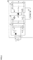
- FIG. 1 is a functional block diagram of an AC-DC converter 100 according to a first embodiment.
- the AC-DC converter 100 functions as a converter that converts power supply electricity from a single-phase AC power supply 2 into output DC electricity.
- the output DC electricity is directly used or is converted into three-phase AC electricity by an inverter to be used to drive various devices, such as pumps, compressors, electric actuators for ships and aircrafts, and robot arms.
- the AC-DC converter 100 includes a rectifier circuit 10, a step-down circuit 20, an inductor 30, a buffer circuit 40, a step-up circuit 50, and a control unit 90.
- the single-phase AC power supply 2 may be a commercial power supply or a power generator, for example.
- the single-phase AC power supply 2 outputs an input voltage v G and an input current i G to the rectifier circuit 10 of the AC-DC converter 100.
- the rectifier circuit 10 is a rectifier circuit that has a power factor correction (PFC) function, and may be implemented using a publicly-known technology.
- the rectifier circuit 10 performs full-wave rectification of the input voltage v G input from the single-phase AC power supply 2 to generate a rectified voltage V R (rectified current i R ). Thereafter, the rectifier circuit 10 removes a highfrequency component from the current waveform by means of the PFC function.
- the rectifier circuit 10 outputs the rectified voltage v R and the rectified current i R to the step-down circuit 20.
- the step-down circuit 20 is disposed subsequent to the rectifier circuit 10 and includes a capacitor C F , a switch T A , and a diode D A . With the switch T A controlled by the control unit 90, the step-down circuit 20 steps down the rectified voltage v R to a step-down circuit voltage v A .
- the step-down circuit 20 outputs an inductor current i L to the inductor 30. The step-down operation performed by the step-down circuit 20 will be detailed later.
- the inductor 30 is a circuit element disposed subsequent to the step-down circuit 20 and may be implemented using a publicly-known technology.
- the inductor 30 accumulates or releases magnetic energy caused by the inductor current i L .
- the buffer circuit 40 is disposed subsequent to the inductor 30.
- the buffer circuit 40 includes an asymmetric full-bridge circuit including a combination of a preceding-side half bridge configured to include a diode D C1 and a switch T C1 , and a subsequent-side half bridge configured to include a diode D C2 and a switch T C2 , with a capacitor C C provided between the half bridges.
- the buffer circuit 40 is connected in series within the AC-DC converter 100 and actively compensates for pulsation of the input electricity. Accordingly, the buffer circuit 40 may be referred to as a "series active buffer", or “series power pulsation buffer” or "SPPB".
- the diodes D C1 and D C2 may be implemented using a publicly-known technology.
- Each of the switches T C1 and T C2 may be implemented by means of a metal-oxide semiconductor field effect transistor (MOS-FET), or may be implemented by means of a wide band gap (WBG) semiconductor, such as gallium nitride (GaN) and silicon carbide (SiC), for higher speed, depending on the required switching speed.
- MOS-FET metal-oxide semiconductor field effect transistor
- WBG wide band gap semiconductor
- GaN gallium nitride
- SiC silicon carbide
- the capacitor C C is a low-capacity capacitor constituted by a film capacitor or a ceramic capacitor, for example, and need not be a high-capacity electrolytic capacitor.
- the step-up circuit 50 is disposed subsequent to the buffer circuit 40 and includes a DC link capacitor C PN , a switch T B , and a diode D B . With the switch T B controlled by the control unit 90, the step-up circuit 50 steps up a buffer capacitor voltage v C to a step-up circuit voltage v B .
- the DC link capacitor C PN is a low-capacity capacitor constituted by a film capacitor or a ceramic capacitor, for example, and need not be a high-capacity electrolytic capacitor.
- the DC link capacitor C PN removes noise caused by switching or the like from the step-up circuit voltage v B and generates a DC link voltage v PN , which is smooth.
- the step-up circuit 50 outputs the DC link voltage v PN thus generated, i.e., an output voltage v PN , to the outside.
- the step-up operation performed by the step-up circuit 50 will be detailed later.
- the control unit 90 includes a buffer voltage controller 92, a DC link voltage controller 94, an inductor voltage controller 96, and a PWM unit 98.
- the control unit 90 controls the step-down circuit 20, the buffer circuit 40, and the step-up circuit 50 to adjust the rectified voltage, the buffer voltage, and the DC link voltage. The control performed by the control unit 90 will be detailed later.
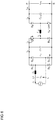
- FIG. 2 is a functional block diagram of an AC-DC converter 200 according to the comparative example.
- the differences from the AC-DC converter 100 illustrated in FIG. 1 are that the buffer circuit 40 is not provided and that the DC link capacitor C PN is constituted by a high-capacity electrolytic capacitor.
- the DC link capacitor C PN compensates for pulsation of input electricity and functions as an energy buffer.
- the buffer circuit 40 of the AC-DC converter 100 on the other hand, merely compensates for pulsation of input electricity and does not function as an energy buffer.
- a control unit 91 in the AC-DC converter 200 controls the step-down circuit 20 and the step-up circuit 50 to adjust the rectified voltage and the DC link voltage.
- the other configurations in the AC-DC converter 200 are identical with those in the AC-DC converter 100.
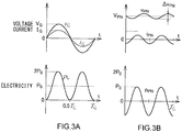
- FIG. 3A shows time variations of the input voltage v G , the input current i G , and input electricity p G in the AC-DC converter 200.
- FIG. 3B shows time variations of the DC link voltage v PN , a DC link capacitor current i PN , and DC link capacitor electricity p PN in the AC-DC converter 200.
- the input voltage (the AC voltage supplied from the single-phase AC power supply 2)
- v G is defined as a sine wave with amplitude V G and a frequency f G , and is expressed as follows.
- v G V G ⁇ sin 2 ⁇ f G t
- the input current i G is controlled to be a sine wave of which the frequency and the phase are identical with those of the input voltage v G .
- the input current i G is expressed as follows.
- i G I G ⁇ sin 2 ⁇ f G t
- the input electricity p G input to the rectifier circuit 10 is expressed as follows.
- the input electricity p G pulsates with a frequency 2f G that is twice the frequency f G of the input voltage v G .
- the DC link capacitor C PN compensates for the pulsation of the input voltage v G by buffering.
- the DC link capacitor C PN accumulates electrostatic energy E C therein.
- E C 1 / 2 ⁇ C PN ⁇ v PN 2 , where C PN is the capacity of the DC link capacitor C PN Accordingly, a capacitor current i C flows through the DC link.
- DC link voltage pulsation ⁇ v PN occurs.
- the DC link voltage pulsation ⁇ v PN vibrates with a frequency 2f G that is twice the frequency f G of the input voltage v G .
- the DC link voltage pulsation ⁇ v PN is dependent on average output electricity ⁇ p PN >, an average DC link voltage ⁇ v PN >, the frequency f G of the input voltage v G , and the capacity C PN of the DC link capacitor C PN , and is expressed as follows.
- ⁇ v PN ⁇ p PN > / 2 ⁇ f G ⁇ 1 / ⁇ v PN > ⁇ C PN Accordingly, to compensate for and restrain the pulsation, the capacity C PN of the DC link capacitor C PN needs to be sufficiently large. To achieve normal inverter functions, the DC link voltage pulsation ⁇ v PN generally needs to be kept within a few percent of the average DC link voltage v PN .
- the capacity of the DC link capacitor C PN needs to be about 3 mF or greater in order to keep ⁇ v PN /v PN within 5 percent.
- a high-capacity electrolytic capacitor is required.
- Such a high-capacity electrolytic capacitor has problems of having a larger size and shorter life. Therefore, the capacity of the DC link capacitor needs to be made small, and the entire device is required to be configured without an electrolytic capacitor.
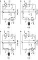
- FIG. 4 illustrates the AC-DC converter 200 during the step-up operation.
- the control unit 91 controls the step-down circuit 20 and the step-up circuit 50 such that the step-up operation is performed when the rectified voltage v R is smaller than the DC link voltage v PN (v R ⁇ v PN ).
- the rectified current i R is controlled to be proportional to the rectified voltage v R (i R ⁇ v R ).
- the PFC rectification and the step-up operation can be simultaneously performed.
- FIG. 5 shows time variations of the input voltage v G , the rectified voltage v R , the DC link voltage v PN , the input current i G , the inductor current i L , an average step-down circuit current ⁇ i A >T SW , an average step-up circuit current ⁇ i B >T SW , the step-down duty cycle d A , the step-up duty cycle d B , output electricity p PN , and DC link capacitor electricity p CPN during the step-up operation.
- ⁇ i A >T SW means a time average of the current i A within a switching period T SW (the same applies hereinafter).
- a time average within a switching period will be abbreviated as an "average”.
- FIG. 6 illustrates the AC-DC converter 200 during the step-down operation.
- the control unit 91 controls the step-down circuit 20 and the step-up circuit 50 such that the step-down operation is performed when the rectified voltage v R is larger than the DC link voltage v PN (v R > v PN ).
- the rectified current i R is controlled to be proportional to the rectified voltage v R (i R ⁇ v R ).
- the electricity p CPN of the DC link capacitor C PN pulsates within ⁇ p PN to compensate for the pulsation of the input electricity. Accordingly, the current i CPN of the DC link capacitor C PN also pulsates within ⁇ i PN .
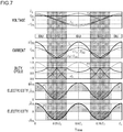
- FIG. 7 shows time variations of the input voltage v G , rectified voltage v R , DC link voltage v PN , input current i G , inductor current i L , average step-down circuit current ⁇ i A >T sw , average step-up circuit current ⁇ i B >T sw , step-down duty cycle d A , step-up duty cycle d B , output electricity p PN , and DC link capacitor electricity p CPN during the step-down operation.
- FIG. 8A illustrates first current control performed by the buffer circuit 40.
- the switches T C1 and T C2 are both turned off.
- the inductor current i L flows through the two diodes D C1 and D C2 , conducting electricity through the capacitor C C in the positive direction.
- i CC i L holds, and the capacitor C C is charged.
- the buffer circuit 40 can use excess voltage in the input for charging.
- the first current control corresponds to a state in which a positive electricity pulsation buffer voltage v PPB is applied in series with the inductor 30.
- FIG. 8B illustrates second current control performed by the buffer circuit 40.
- the switches T C1 and T C2 are both turned on.
- the inductor current i L flows through the two switches T C1 and T C2 , conducting electricity through the capacitor C C in the negative direction.
- i CC -i L holds, and the capacitor C C is discharged.
- the buffer circuit 40 can provide the charged electric charges to the output side.
- the second current control corresponds to a state in which a negative electricity pulsation buffer voltage v PPB is applied in series with the inductor 30.
- FIGS. 8C and 8D respectively illustrate third and fourth current control performed by the buffer circuit 40.
- the switch T C1 is turned on, and the switch T C2 is turned off.
- the switch T C1 is turned off, and the switch T C2 is turned on.
- the inductor current i L flows bypassing the capacitor C C .
- i CC 0 holds, and the capacitor C C is neither charged nor discharged.
- Each of the third and fourth current control corresponds to a state in which zero voltage is applied in series with the inductor 30.
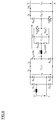
- FIG. 9 illustrates the AC-DC converter 100 during the step-up operation.
- the control unit 90 controls the step-down circuit 20, the buffer circuit 40, and the step-up circuit 50 such that the step-up operation is performed when the rectified current i R is larger than the average step-up circuit current ⁇ i B >T SW (i.e., when m I > 1 holds).
- the rectified current i R is controlled to be proportional to the rectified voltage v R (i R oc v R ).
- the inductor current i L is converted into the step-up circuit current i B .
- i L v PN / ⁇ v B > T SW ⁇ ⁇ i B > T SW can be derived. Accordingly, when v PN > ⁇ v B >T SW holds (i.e., when the low voltage ⁇ v B >T SW is stepped up to the high voltage v PN ), the inductor current i L (i.e., the rectified current i R ) is found to be larger than the average step-up circuit current ⁇ i B >T SW .
- the step-up operation is performed, irrespective of the ratio of the rectified voltage v R to the output voltage (DC link voltage) v BN .
- the buffer circuit 40 switches the first current control (charging) and the fourth current control (no charging and no discharging) at a high frequency. Accordingly, the buffer circuit 40 functions as a voltage source, enabling output of a constant output voltage v PN .
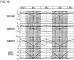
- FIG. 10 shows time variations of the input voltage v G , rectified voltage v R , DC link voltage v PN , input current i G , inductor current i L , average step-down circuit current ⁇ i A >T sw , average step-up circuit current ⁇ i B >T sw , step-down duty cycle d A , and step-up duty cycle d B during the step-up operation.
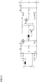
- FIG. 11 illustrates the AC-DC converter 100 during the step-down operation.
- the control unit 90 controls the step-down circuit 20, the buffer circuit 40, and the step-up circuit 50 such that the step-down operation is performed when the rectified current i R is smaller than the average step-up circuit current ⁇ i B >T SW (i.e., when m I ⁇ 1 holds).
- the rectified current i R is controlled to be proportional to the rectified voltage v R (i R oc v R ).
- the average step-down circuit current ⁇ i A >T SW i.e., the rectified current i R
- the inductor current i L i.e., the step-up circuit current ⁇ i B >T SW ).
- the step-down operation is performed, irrespective of the ratio of the rectified voltage v R to the output voltage (DC link voltage) V PN .
- the buffer circuit switches the second current control (discharging) and the third current control (no charging and no discharging) at a high frequency. Accordingly, the buffer circuit 40 functions as a voltage source, enabling output of the output voltage v PN .
- FIG. 12 shows time variations of the input voltage v G , rectified voltage v R , DC link voltage v PN , input current i G , inductor current i L , average step-down circuit current ⁇ i A >T sw , average step-up circuit current ⁇ i B >T sw , step-down duty cycle d A , and step-up duty cycle d B during the step-down operation.
- the inductor current i L is expressed as follows.
- i L max i R , ⁇ i B > T SW , where max(a,b) means a larger value between a and b.
- the inductor current i L obtained in this manner is smaller than the inductor current i L obtained in the AC-DC converter 200.
- the step-down duty cycle d A and the step-up duty cycle d B are defined with the modulation rate m I as follows.
- d A min m I 1
- d B 1 ⁇ min 1 / m I , 1 where min(a,b) means a smaller value between a and b
- the buffer circuit 40 applies the buffer voltage v PPB that satisfies the following condition.
- ⁇ v PPB > T SW ⁇ v A > T SW ⁇ ⁇ v B > T SW
- Each of the switch node voltage ⁇ v A >T sw in the step-down operation and the switch node voltage ⁇ v B >T SW in the step-up operation is defined by the modulation rate m I .
- a buffer duty cycle d C is defined as ratio of the average buffer voltage ⁇ v PPB >T SW to the buffer capacitor voltage v C .
- d C ⁇ v PPB > T SW / v C
- v PPB > T SW ⁇ v C i . e . , ⁇ 1 ⁇ d C ⁇ 1 always holds.
- the minimum value of the buffer capacitor voltage v C is defined by the maximum value of the average buffer voltage ⁇ v PPB >T SW .
- the buffer circuit 40 needs to fully compensate for the DC link voltage v PN . Therefore, v C > v PN always holds.
- a duty cycle d C1 of the preceding-side half bridge (hereinafter, referred to as the "first buffer duty cycle d C1 ”) and a duty cycle d C2 of the subsequent-side half bridge (hereinafter, referred to as the “second buffer duty cycle d C2 ”) in the buffer circuit 40 are obtained based on the buffer duty cycle d C .
- the buffer duty cycle d C vibrates with a frequency that is twice the frequency of pulsation of the input electricity p G .
- FIG. 13 shows time variations of buffer capacitor electricity p CC , the DC link capacitor electricity p CPN , the buffer capacitor voltage v C , the average buffer voltage ⁇ v PPB >T SW , the buffer duty cycle d C , the first buffer duty cycle d C1 , and the second buffer duty cycle d C2 .
- calculating the step-down duty cycle d A , the step-up duty cycle d B , the first buffer duty cycle d C1 , and the second buffer duty cycle d C2 and controlling the step-down circuit 20, the buffer circuit 40, and the step-up circuit 50 can compensate for the pulsation of the input AC electricity and generate a desired magnitude of DC electricity. Since the capacitor C C in the buffer circuit 40 need not have large capacity, the capacitor C C can be implemented by a film capacitor or a ceramic capacitor, for example, instead of an electrolytic capacitor.
- FIG. 14 is a functional block diagram of the control unit 90 in the AC-DC converter 100.
- the control unit 90 includes the buffer voltage controller 92, the DC link voltage controller 94, the inductor voltage controller 96, and the PWM unit 98.
- a target buffer capacitor voltage v C * is input and also an average buffer capacitor voltage ⁇ v C > from a filter F VC is input.
- the average buffer capacitor voltage difference ⁇ v C > is input to a voltage controller R VC and converted into a target average buffer capacitor current ⁇ i CC *> ( ⁇ v C > ⁇ ⁇ i CC *>).
- the average target input electricity ⁇ p G *> is multiplied by 2.
- , and the square of the reciprocal of an average input voltage ⁇ v G >), so that a target rectified current i R * is calculated (i R * ⁇ p G *> ⁇ 2 ⁇
- the target rectified current i R * is output to the inductor voltage controller 96.
- a target DC link voltage v PN * is input and also the DC link voltage v PN from the step-up circuit 50 is input.
- the DC link voltage difference ⁇ v PN is input to a voltage controller R vPN and converted into a target capacitor current i CPN * ( ⁇ v PN ⁇ i CPN *).
- the target step-up circuit electricity p B * is input to the filter F PB . From the filter F PB , the average target step-up circuit electricity ⁇ p B *> is output.
- the other of the two branched target step-up circuit currents i B * is output to the inductor voltage controller 96.
- the target rectified current i R *, the target step-up circuit current i B *, the inductor current i L , and the buffer capacitor voltage v C are input.
- the target rectified current i R * thus input is branched into three currents.
- the other of the three branched target rectified currents i R * is compared in value with the target step-up circuit current i B *.
- the target step-up circuit current i B * input is branched into three currents.
- the other of the three branched target step-up circuit currents i B * is compared in value with the target rectified current i R *.
- the step-down duty cycle d A is branched into two cycles.
- One of the two branched step-down duty cycles d A is output to the PWM unit 98.
- the other of the two branched step-down duty cycles d A is multiplied by the absolute value of the input voltage v G ,
- , so that the step-down circuit voltage v A is calculated (v A d A ⁇
- the amount 1-d B on which the step-up duty cycle d B is based is branched into two amounts.
- One of the two branched amounts 1-d B is converted into the step-up duty cycle d B and then output to the PWM unit 98 (1-d B ⁇ d B ).
- the inductor current difference ⁇ i L is input to a voltage controller R IL and converted into a target inductor voltage v L * ( ⁇ i L ⁇ v L *).
- the buffer duty cycle d C thus calculated is output to the PWM unit 98.
- the step-down duty cycle d A , the step-up duty cycle d B , and the buffer duty cycle d C are input.
- the PWM unit 98 Based on the step-down duty cycle d A , the step-up duty cycle d B , and the buffer duty cycle d C , the PWM unit 98 performs pulse width modulation to generate a step-down circuit switching signal S A , a step-up circuit switching signal S B , a first buffer switching signal S C1 , and a second buffer switching signal S C2 .
- the PWM unit 98 outputs the step-down circuit switching signal S A to the step-down circuit 20, the step-up circuit switching signal S B to the step-up circuit 50, and the first buffer switching signal S C1 and the second buffer switching signal S C2 to the buffer circuit 40.
- a desired magnitude of DC electricity can be generated from single-phase AC electricity, without requiring an electrolytic capacitor.
- Each of the switches T C1 and T C2 in the buffer circuit 40 may be implemented by means of a WBG semiconductor, such as GaN and SiC.
- the switching speed of a WBG semiconductor is about ten times faster than that of a conventional Si-based MOS-FET. Accordingly, by using WBG semiconductors for the switches T C1 and T C2 in the buffer circuit 40, a desired magnitude of DC electricity can be generated from single-phase AC electricity with high frequency.
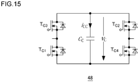
- the buffer circuit may include an asymmetric full-bridge circuit including a combination of a preceding-side half bridge configured to include the switch T C1 and a switch T C3 , and a subsequent-side half bridge configured to include the switch T C2 and a switch T C4 , with the capacitor C C provided between the half bridges.
- the buffer circuit may include T C3 instead of the diode D C1 of the buffer circuit 40 and may include the switch T C4 instead of the diode D C2 of the buffer circuit 40.
- FIG. 15 schematically illustrates a buffer circuit 48 configured in that way.
- the buffer circuit 48 enables the aforementioned four types of current control by combining ON and OFF of the switches T C1 , T C2 , T C3 , and T C4 .
- switches instead of diodes, faster switching can be performed.
- a desired magnitude of DC electricity can be generated from single-phase AC electricity with higher frequency.
- the buffer circuit may be configured by adding half bridges in parallel to the buffer circuit 40 illustrated in FIG. 1 .
- FIG. 16 schematically illustrates a buffer circuit 49a configured in that way.
- the buffer circuit 49a includes an asymmetric full-bridge circuit including a combination of preceding-side half bridges configured to include diodes D C11 , D C12 , ..., and D C1n and switches T C11 , T C12 , ..., and T C1n , and subsequent-side half bridges configured to include diodes D C21 , D C22 , ..., and D C2n and switches T C21 , T C22 , ..., and T C2n , with the capacitor C C provided between the half bridges, where n is an integer greater than or equal to 2.
- the buffer circuit 49a is configured by adding n preceding-side half bridges and n subsequent-side half bridges in parallel to the buffer circuit 40.
- the buffer circuit 49a also enables the aforementioned four types of current control by combining ON and OFF of the switches T C11 , T C12 , ..., and T C1n , and the switches T C21 , T C22 , ..., and T C2n .
- the buffer circuit 49a is configured by adding half bridges in parallel to a preceding-side half bridge and a subsequent-side half bridge, thereby reducing the switching load on each switch. Therefore, the switching speed of each switch may be slower than that of each switch in the buffer circuit 40. With this configuration, using switches of which the speed is relatively slow, a desired magnitude of DC electricity can be generated from single-phase AC electricity with high frequency.
- the buffer circuit may be configured by adding half bridges in parallel to the buffer circuit 48 illustrated in FIG. 15 .
- FIG. 17 schematically illustrates a buffer circuit 49b configured in that way.
- the buffer circuit 49b includes an asymmetric full-bridge circuit including a combination of preceding-side half bridges configured to include the switches T C11 , T C12 , ..., and T C1n and switches T C31 , T C32 , ..., and T C3n , and subsequent-side half bridges configured to include the switches T C21 , T C22 , ..., and T C2n and switches T C41 , T C42 , ..., and T C4n , with the capacitor C C provided between the half bridges, where n is an integer greater than or equal to 2.
- the buffer circuit 49b is configured by adding n preceding-side half bridges and n subsequent-side half bridges in parallel to the buffer circuit 48.
- the buffer circuit 49b also enables the aforementioned four types of current control by combining ON and OFF of the switches T C11 , T C12 , ..., and T C1n and the switches T C31 , T C32 , ..., and T C3n , and the switches T C21 , T C22 , ..., and T C2n and the switches T C41 , T C42 , ..., and T C4n .
- the buffer circuit 49b is configured by adding half bridges in parallel to a preceding-side half bridge and a subsequent-side half bridge, thereby reducing the switching load on each switch. Therefore, the switching speed of each switch may be slower than that of each switch in the buffer circuit 48. With this configuration, using switches of which the speed is relatively slow, a desired magnitude of DC electricity can be generated from single-phase AC electricity with higher frequency.
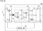
- FIG. 18 is a functional block diagram of a DC-DC converter 300 according to a second embodiment.
- the DC-DC converter 300 functions as a converter that converts electricity from a DC power supply 3 into other DC electricity.
- the converted DC electricity is directly used or is converted into three-phase AC electricity by an inverter to be used to drive various devices, such as pumps, compressors, electric actuators for ships and aircrafts, and robot arms.
- the DC-DC converter 300 includes the step-down circuit 20, the inductor 30, a buffer circuit 42, the step-up circuit 50, and the control unit 90.
- the DC-DC converter 300 differs from the AC-DC converter 100 in that the rectifier circuit 10 is not provided. Since the configurations and operations of the step-down circuit 20, the inductor 30, the step-up circuit 50, and the control unit 90 are identical with those in the AC-DC converter 100, the explanation thereof will be omitted.
- the buffer circuit 42 includes an asymmetric full-bridge circuit including a combination of a preceding-side half bridge configured to include the diode D C1 and the switch T C1 , and a subsequent-side half bridge configured to include the diode D C2 and the switch T C2 , with the capacitor C C provided between the half bridges.
- an input voltage at an input frequency of 50-60 kHz is input from a commercial single-phase AC power supply.
- each of the switches T C1 and T C2 in the buffer circuit 40 operates at a switching frequency in the range of 10 kHz to 100 kHz.
- each of the switches T C1 and T C2 in the buffer circuit 42 operates at a switching frequency that is about ten times the ripple frequency, i.e., in the range of 1 MHz to 2 MHz. Therefore, each of the switches T C1 and T C2 in the buffer circuit 42 is constituted by a high speed WBG semiconductor, such as GaN and SiC.
- a desired magnitude of DC electricity can be generated by compensating for the ripple in DC electricity from a DC power supply, without requiring an electrolytic capacitor.
- FIG. 19 is a functional block diagram of an AC-AC converter 400 according to a third embodiment.
- the AC-AC converter 400 functions as a converter that converts electricity from the single-phase AC power supply 2 into three-phase AC electricity.
- the three-phase AC electricity thus converted is used to drive various devices, such as pumps, compressors, electric actuators for ships and aircrafts, and robot arms.
- the AC-AC converter 400 includes the rectifier circuit 10, the step-down circuit 20, the inductor 30, the buffer circuit 40, the step-up circuit 50, an inverter 60, and the control unit 90.
- the rectifier circuit 10 Since the configurations and operations of the rectifier circuit 10, the step-down circuit 20, the inductor 30, the buffer circuit 40, the step-up circuit 50, and the control unit 90 are identical with those in the AC-DC converter 100, the explanation thereof will be omitted.
- the inverter 60 generates three-phase AC voltages from the DC link voltage v PN .
- the inverter 60 may be implemented using a publicly-known technology.
- the three-phase AC voltages are constituted by a U phase, a V phase, and a W phase, which alternate with a phase difference of 2n/3, for example.
- a desired magnitude of three-phase AC electricity can be generated from single-phase AC electricity, without requiring an electrolytic capacitor.
- the AC-DC converter includes one buffer circuit provided subsequent to a diode.
- the configuration is not limited thereto, and the AC-DC converter may include multiple buffer circuits subsequent to a diode. According to this modification, the processing load on each buffer circuit can be reduced, so that a desired magnitude of DC electricity can be generated from single-phase AC electricity with higher frequency.
- the AC-DC converter compensates for pulsation of an input voltage that vibrates with a frequency that is twice the frequency of the input voltage.
- the operation is not limited thereto, and the AC-DC converter may compensate for a high frequency component of input electricity pulsation, such as a frequency that is four times (secondary high frequency), eight times (quaternary high frequency), or twelve times (senary high frequency) the input voltage frequency.
- a high frequency component of input electricity pulsation such as a frequency that is four times (secondary high frequency), eight times (quaternary high frequency), or twelve times (senary high frequency) the input voltage frequency.
- the present invention relates to an AC-DC converter, a DC-DC converter, and an AC-AC converter that convert electricity.
Landscapes
- Engineering & Computer Science (AREA)
- Power Engineering (AREA)
- Rectifiers (AREA)
- Dc-Dc Converters (AREA)
- Ac-Ac Conversion (AREA)
- Inverter Devices (AREA)
Abstract
Description
- The present invention relates to an AC-DC converter, a DC-DC converter, and an AC-AC converter that convert electricity.
- As an AC-DC converter for converting electricity supplied from a single-phase AC power supply into DC electricity, an AC-DC converter provided with a rectifier circuit and a smoothing capacitor has been disclosed (see
Patent Literature 1, for example). - Patent Literature 1:
Japanese Unexamined Patent Application Publication No. 2016-067199 - In household electric appliances and industrial equipment, electricity supplied from a single-phase AC power supply is generally converted into DC electricity by means of an AC-DC converter, and the DC electricity is then converted by an inverter into three-phase AC electricity to be used for motor control. Such an AC-DC converter is generally configured to include a rectifier circuit that converts electricity supplied from an AC power supply into DC electricity. However, such conversion from single-phase AC electricity to DC electricity naturally causes a difference between the input electricity and the output electricity, which then causes pulsation of electricity. To absorb and compensate for the pulsation, a buffer is necessary. Conventionally, such a buffer has been generally constituted by a high-capacity DC link capacitor. In this case, the capacitance required for the DC link capacitor is significantly large. For example, when the operating frequency is the order of kW and the power supply voltage is 100 V, the capacitance of the DC link capacitor will be of the order of mF. To achieve this, a high-capacity electrolytic capacitor needs to be used. However, because of its larger size and shorter life, an electrolytic capacitor has large disadvantages in size, cost, and life of equipment. Accordingly, there is a need for an AC-DC converter in which an electrolytic capacitor is not required for the DC link capacitor.
- The present invention has been made in view of such an issue, and a purpose thereof is to achieve an electrolytic-capacitorless AC-DC converter with a low-capacity DC link capacitor.
- In response to the above issue, an AC-DC converter of one aspect of the present invention includes: a rectifier circuit that rectifies an AC voltage to generate a rectified voltage; a step-down circuit that steps down the rectified voltage; an inductor; a buffer circuit that includes an asymmetric full-bridge circuit including a combination of a preceding-side half bridge configured to include a first diode and a first switch, and a subsequent-side half bridge configured to include a second diode and a second switch, with a capacitor provided between the preceding-side half bridge and the subsequent-side half bridge, and that generates a DC voltage from the rectified voltage; and a step-up circuit that steps up a voltage of the buffer circuit.
- Another aspect of the present invention also relates to an AC-DC converter. The AC-DC converter includes: a rectifier circuit that rectifies an AC voltage to generate a rectified voltage; a step-down circuit that steps down the rectified voltage; an inductor; a buffer circuit that includes an asymmetric full-bridge circuit including a combination of a preceding-side half bridge configured to include a first switch and a third switch, and a subsequent-side half bridge configured to include a second switch and a fourth switch, with a capacitor provided between the preceding-side half bridge and the subsequent-side half bridge, and that generates a DC voltage from the rectified voltage; and a step-up circuit that steps up a voltage of the buffer circuit.
- Yet another aspect of the present invention relates to a DC-DC converter. The DC-DC converter includes: a step-down circuit that steps down a first DC voltage; an inductor; a buffer circuit that includes an asymmetric full-bridge circuit including a combination of a preceding-side half bridge configured to include a first diode and a first switch, and a subsequent-side half bridge configured to include a second diode and a second switch, with a capacitor provided between the preceding-side half bridge and the subsequent-side half bridge, and that generates a second DC voltage from the first DC voltage; and a step-up circuit that steps up a voltage of the buffer circuit.
- Still yet another aspect of the present invention relates to an AC-AC converter. The AC-AC converter includes: a rectifier circuit that rectifies a first AC voltage to generate a rectified voltage; a step-down circuit that steps down the rectified voltage; an inductor; a buffer circuit that includes an asymmetric full-bridge circuit including a combination of a preceding-side half bridge configured to include a first diode and a first switch, and a subsequent-side half bridge configured to include a second diode and a second switch, with a capacitor provided between the preceding-side half bridge and the subsequent-side half bridge, and that generates a DC voltage from the first AC voltage; a step-up circuit that steps up a voltage of the buffer circuit; and an inverter that converts the DC voltage into a second AC voltage.
- Optional combinations of the aforementioned constituting elements, and implementation of the present invention, including the constituting elements and expressions, in the form of methods, apparatuses, programs, transitory or non-transitory storage medium storing programs, or systems may also be practiced as additional modes of the present invention.
- The present invention achieves an electrolytic-capacitorless AC-DC converter with a low-capacity DC link capacitor.
- Embodiments will now be described, by way of example only, with reference to the accompanying drawings which are meant to be exemplary, not limiting, and wherein like elements are numbered alike in several Figures, in which:
-
FIG. 1 is a functional block diagram that illustrates an AC-DC converter according to an embodiment; -
FIG. 2 is a functional block diagram that illustrates an AC-DC converter according to a comparative example; -
FIGS. 3 are diagrams that each show time variations of a voltage, a current, and electricity of the AC-DC converter illustrated inFIG. 2 , in whichFIG. 3A shows time variations of an input voltage, an input current, and input electricity, andFIG. 3B shows time variations of a DC link voltage, a DC link capacitor current, and DC link capacitor electricity; -
FIG. 4 is a diagram that illustrates a step-up operation in the AC-DC converter illustrated inFIG. 2 ; -
FIG. 5 is a diagram that shows time variations of the input voltage, a rectified voltage, the DC link voltage, the input current, an inductor current, an average step-down circuit switch current, an average step-up circuit switch current, a duty cycle, output electricity, and the DC link capacitor electricity during the step-up operation illustrated inFIG. 4 ; -
FIG. 6 is a diagram that illustrates a step-down operation in the AC-DC converter illustrated inFIG. 2 ; -
FIG. 7 is a diagram that shows time variations of the input voltage, rectified voltage, DC link voltage, input current, inductor current, average step-down circuit switch current, average step-up circuit switch current, duty cycle, output electricity, and DC link capacitor electricity during the step-down operation illustrated inFIG. 6 ; -
FIGS. 8 are diagrams that each illustrate current control performed by a buffer circuit in the AC-DC converter illustrated inFIG. 1 , in whichFIG. 8A illustrates first current control,FIG. 8B illustrates second current control,FIG. 8C illustrates third current control, andFIG. 8D illustrates fourth current control; -
FIG. 9 is a diagram that illustrates the step-up operation in the AC-DC converter illustrated inFIG. 1 ; -
FIG. 10 is a diagram that shows time variations of the input voltage, rectified voltage, DC link voltage, input current, inductor current, average step-down circuit switch current, average step-up circuit switch current, and duty cycle during the step-up operation illustrated inFIG. 9 ; -
FIG. 11 is a diagram that illustrates the step-down operation in the AC-DC converter illustrated inFIG. 1 ; -
FIG. 12 is a diagram that shows time variations of the input voltage, rectified voltage, DC link voltage, input current, inductor current, average step-down circuit switch current, average step-up circuit switch current, and duty cycle during the step-down operation illustrated inFIG. 11 ; -
FIG. 13 is a diagram that shows time variations of buffer capacitor electricity, the DC link capacitor electricity, a buffer capacitor voltage, an average buffer voltage, a buffer duty cycle, a first buffer duty cycle, and a second buffer duty cycle of the AC-DC converter illustrated inFIG. 1 ; -
FIG. 14 is a functional block diagram that illustrates a control unit in the AC-DC converter illustrated inFIG. 1 ; -
FIG. 15 is a schematic diagram that illustrates a buffer circuit in the AC-DC converter according to the embodiment; -
FIG. 16 is a schematic diagram that illustrates another buffer circuit in the AC-DC converter according to the embodiment; -
FIG. 17 is a schematic diagram that illustrates yet another buffer circuit in the AC-DC converter according to the embodiment; -
FIG. 18 is a functional block diagram that illustrates a DC-DC converter according to an embodiment; and -
FIG. 19 is a functional block diagram that illustrates an AC-AC converter according to an embodiment. - In the following embodiments, like reference characters denote like constituting elements, and repetitive description will be omitted. Also, for the sake of convenience, part of the constituting elements may be appropriately omitted in each drawing. Unless otherwise specified, for a numerical value A, <A> denotes an average value of A, and A* denotes a target value of A. In the present specification, along a flow of current or a signal from the power supply side toward the output side, the upstream side may be referred to using "preceding" or "input", and the downstream side may be referred to using "subsequent" or "output".
-
FIG. 1 is a functional block diagram of an AC-DC converter 100 according to a first embodiment. The AC-DC converter 100 functions as a converter that converts power supply electricity from a single-phaseAC power supply 2 into output DC electricity. The output DC electricity is directly used or is converted into three-phase AC electricity by an inverter to be used to drive various devices, such as pumps, compressors, electric actuators for ships and aircrafts, and robot arms. The AC-DC converter 100 includes arectifier circuit 10, a step-down circuit 20, aninductor 30, abuffer circuit 40, a step-upcircuit 50, and acontrol unit 90. - The single-phase
AC power supply 2 may be a commercial power supply or a power generator, for example. The single-phaseAC power supply 2 outputs an input voltage vG and an input current iG to therectifier circuit 10 of the AC-DC converter 100. - The
rectifier circuit 10 is a rectifier circuit that has a power factor correction (PFC) function, and may be implemented using a publicly-known technology. Therectifier circuit 10 performs full-wave rectification of the input voltage vG input from the single-phaseAC power supply 2 to generate a rectified voltage VR (rectified current iR). Thereafter, therectifier circuit 10 removes a highfrequency component from the current waveform by means of the PFC function. Therectifier circuit 10 outputs the rectified voltage vR and the rectified current iR to the step-down circuit 20. - The step-
down circuit 20 is disposed subsequent to therectifier circuit 10 and includes a capacitor CF, a switch TA, and a diode DA. With the switch TA controlled by thecontrol unit 90, the step-down circuit 20 steps down the rectified voltage vR to a step-down circuit voltage vA. The step-down circuit 20 outputs an inductor current iL to theinductor 30. The step-down operation performed by the step-down circuit 20 will be detailed later. - The
inductor 30 is a circuit element disposed subsequent to the step-down circuit 20 and may be implemented using a publicly-known technology. Theinductor 30 accumulates or releases magnetic energy caused by the inductor current iL. - The
buffer circuit 40 is disposed subsequent to theinductor 30. Thebuffer circuit 40 includes an asymmetric full-bridge circuit including a combination of a preceding-side half bridge configured to include a diode DC1 and a switch TC1, and a subsequent-side half bridge configured to include a diode DC2 and a switch TC2, with a capacitor CC provided between the half bridges. Thebuffer circuit 40 is connected in series within the AC-DC converter 100 and actively compensates for pulsation of the input electricity. Accordingly, thebuffer circuit 40 may be referred to as a "series active buffer", or "series power pulsation buffer" or "SPPB". The diodes DC1 and DC2 may be implemented using a publicly-known technology. Each of the switches TC1 and TC2 may be implemented by means of a metal-oxide semiconductor field effect transistor (MOS-FET), or may be implemented by means of a wide band gap (WBG) semiconductor, such as gallium nitride (GaN) and silicon carbide (SiC), for higher speed, depending on the required switching speed. The capacitor CC is a low-capacity capacitor constituted by a film capacitor or a ceramic capacitor, for example, and need not be a high-capacity electrolytic capacitor. - The step-up
circuit 50 is disposed subsequent to thebuffer circuit 40 and includes a DC link capacitor CPN, a switch TB, and a diode DB. With the switch TB controlled by thecontrol unit 90, the step-upcircuit 50 steps up a buffer capacitor voltage vC to a step-up circuit voltage vB. The DC link capacitor CPN is a low-capacity capacitor constituted by a film capacitor or a ceramic capacitor, for example, and need not be a high-capacity electrolytic capacitor. The DC link capacitor CPN removes noise caused by switching or the like from the step-up circuit voltage vB and generates a DC link voltage vPN, which is smooth. The step-upcircuit 50 outputs the DC link voltage vPN thus generated, i.e., an output voltage vPN, to the outside. The step-up operation performed by the step-upcircuit 50 will be detailed later. - The
control unit 90 includes abuffer voltage controller 92, a DClink voltage controller 94, aninductor voltage controller 96, and aPWM unit 98. Thecontrol unit 90 controls the step-down circuit 20, thebuffer circuit 40, and the step-upcircuit 50 to adjust the rectified voltage, the buffer voltage, and the DC link voltage. The control performed by thecontrol unit 90 will be detailed later. - Before the voltage control performed by the AC-DC converter according to the embodiment is described, voltage control performed by an AC-DC converter according to a comparative example will be described.
FIG. 2 is a functional block diagram of an AC-DC converter 200 according to the comparative example. The differences from the AC-DC converter 100 illustrated inFIG. 1 are that thebuffer circuit 40 is not provided and that the DC link capacitor CPN is constituted by a high-capacity electrolytic capacitor. In the AC-DC converter 200, the DC link capacitor CPN compensates for pulsation of input electricity and functions as an energy buffer. Thebuffer circuit 40 of the AC-DC converter 100, on the other hand, merely compensates for pulsation of input electricity and does not function as an energy buffer. Acontrol unit 91 in the AC-DC converter 200 controls the step-down circuit 20 and the step-upcircuit 50 to adjust the rectified voltage and the DC link voltage. The other configurations in the AC-DC converter 200 are identical with those in the AC-DC converter 100. -
FIG. 3A shows time variations of the input voltage vG, the input current iG, and input electricity pG in the AC-DC converter 200.FIG. 3B shows time variations of the DC link voltage vPN, a DC link capacitor current iPN, and DC link capacitor electricity pPN in the AC-DC converter 200. - In the present specification, the input voltage (the AC voltage supplied from the single-phase AC power supply 2) vG is defined as a sine wave with amplitude VG and a frequency fG, and is expressed as follows.


rectifier circuit 10 is expressed as follows.
- As described below, the DC link capacitor CPN compensates for the pulsation of the input voltage vG by buffering. The DC link capacitor CPN accumulates electrostatic energy EC therein.


-
FIG. 4 illustrates the AC-DC converter 200 during the step-up operation. Thecontrol unit 91 controls the step-down circuit 20 and the step-upcircuit 50 such that the step-up operation is performed when the rectified voltage vR is smaller than the DC link voltage vPN (vR < vPN). During the step-up operation, the switch TA in the step-down circuit 20 is continuously turned on (TA = ON). Accordingly, a step-down duty cycle dA is 1 (dA = 1). Meanwhile, the switch TB in the step-upcircuit 50 operates at a high frequency (HF) (TB = HF). The modulation rate mI is vR/vPN, with which a step-up duty cycle dB is calculated (dB = mI = vR/vPN). To perform the PFC operation, the rectified current iR is controlled to be proportional to the rectified voltage vR (iR ∝ vR). At the time, the rectified current iR is equal to the input current iG (iR = iG). As describe above, since the switch TA is continuously turned on during the step-up operation, the rectified current iR becomes equal to the inductor current iL. Accordingly, iL = iA = iR = iG holds. As described above, by performing high frequency control of the switch TB in the step-upcircuit 50 such that iL = iG holds, the PFC rectification and the step-up operation can be simultaneously performed. -
FIG. 5 (not hatched area) shows time variations of the input voltage vG, the rectified voltage vR, the DC link voltage vPN, the input current iG, the inductor current iL, an average step-down circuit current <iA>TSW, an average step-up circuit current <iB>TSW, the step-down duty cycle dA, the step-up duty cycle dB, output electricity pPN, and DC link capacitor electricity pCPN during the step-up operation. In the above, <iA>TSW means a time average of the current iA within a switching period TSW (the same applies hereinafter). In the following, a time average within a switching period will be abbreviated as an "average". -
FIG. 6 illustrates the AC-DC converter 200 during the step-down operation. Thecontrol unit 91 controls the step-down circuit 20 and the step-upcircuit 50 such that the step-down operation is performed when the rectified voltage vR is larger than the DC link voltage vPN (vR > vPN). During the step-down operation, the switch TB in the step-upcircuit 50 is continuously turned off (TB = OFF) . Accordingly, the step-up duty cycle dB is 0 (dB = 0) . Meanwhile, the switch TA in the step-down circuit 20 operates at a high frequency (TA = HF). The modulation rate mI is vR/vPN, with which the step-down duty cycle dA is calculated (dA = mI = vR/vPN). To perform the PFC operation, the rectified current iR is controlled to be proportional to the rectified voltage vR (iR ∝ vR). Differently from the step-up operation, since the switch TA operates at a high frequency, the inductor current iL is not equal to the rectified current iR but is equal to a step-up circuit current iB (iL ≠ iR, iL = iB = iCPN+iPN). The electricity pCPN of the DC link capacitor CPN pulsates within ±pPN to compensate for the pulsation of the input electricity. Accordingly, the current iCPN of the DC link capacitor CPN also pulsates within ±iPN. As described above, by performing high frequency control of the switch TA in the step-down circuit 20 such that iL = iCPN+iPN holds, the PFC rectification and the step-down operation can be simultaneously performed. -
FIG. 7 (not hatched area) shows time variations of the input voltage vG, rectified voltage vR, DC link voltage vPN, input current iG, inductor current iL, average step-down circuit current <iA>Tsw, average step-up circuit current <iB>Tsw, step-down duty cycle dA, step-up duty cycle dB, output electricity pPN, and DC link capacitor electricity pCPN during the step-down operation. - The voltage control in the embodiment will now be described. The
buffer circuit 40 in the AC-DC converter 100 illustrated inFIG. 1 can perform four types of current control by combining ON and OFF of the switches TC1 and TC2.FIG. 8A illustrates first current control performed by thebuffer circuit 40. During the first current control, the switches TC1 and TC2 are both turned off. The inductor current iL flows through the two diodes DC1 and DC2, conducting electricity through the capacitor CC in the positive direction. At the time, iCC = iL holds, and the capacitor CC is charged. Thus, in the first current control, thebuffer circuit 40 can use excess voltage in the input for charging. The first current control corresponds to a state in which a positive electricity pulsation buffer voltage vPPB is applied in series with theinductor 30.FIG. 8B illustrates second current control performed by thebuffer circuit 40. During the second current control, the switches TC1 and TC2 are both turned on. The inductor current iL flows through the two switches TC1 and TC2, conducting electricity through the capacitor CC in the negative direction. At the time, iCC = -iL holds, and the capacitor CC is discharged. Thus, in the second current control, thebuffer circuit 40 can provide the charged electric charges to the output side. The second current control corresponds to a state in which a negative electricity pulsation buffer voltage vPPB is applied in series with theinductor 30.FIGS. 8C and 8D respectively illustrate third and fourth current control performed by thebuffer circuit 40. During the third current control, the switch TC1 is turned on, and the switch TC2 is turned off. During the fourth current control, the switch TC1 is turned off, and the switch TC2 is turned on. During the third and fourth current control, the inductor current iL flows bypassing the capacitor CC. At the time, iCC = 0 holds, and the capacitor CC is neither charged nor discharged. Each of the third and fourth current control corresponds to a state in which zero voltage is applied in series with theinductor 30. - In the AC-
DC converter 200, the modulation rate mI is calculated as ratio of the rectified voltage vR to the output voltage (DC link voltage) vPN (mI = vR/vPN). Such a method of calculating the modulation rate based on voltage ratio may be sometimes called a "voltage conversion approach". Meanwhile, in the AC-DC converter 100, the modulation rate mI is calculated as ratio of the rectified current iR to an average value <iB>TSW of the step-up circuit current iB within a switching period (mI = iR/<iB>TSW). Such a method of calculating the modulation rate based on current ratio may be sometimes called a "current conversion approach". -
FIG. 9 illustrates the AC-DC converter 100 during the step-up operation. Thecontrol unit 90 controls the step-down circuit 20, thebuffer circuit 40, and the step-upcircuit 50 such that the step-up operation is performed when the rectified current iR is larger than the average step-up circuit current <iB>TSW (i.e., when mI > 1 holds). During the step-up operation, the switch TA in the step-down circuit 20 is continuously turned on (TA = ON). Accordingly, the step-down duty cycle dA is 1 (dA = 1) . - Meanwhile, the switch TB in the step-up
circuit 50 operates at a high frequency (TB = HF). To perform the PFC operation, the rectified current iR is controlled to be proportional to the rectified voltage vR (iR oc vR). At the time, the rectified current iR is equal to the input current iG (iR = iG). As describe above, since the switch TA is continuously turned on during the step-up operation, the rectified current iR becomes equal to the inductor current iL. Accordingly, iL = iA = iR = iG holds. As a result of the step-up operation, the inductor current iL is converted into the step-up circuit current iB. The average step-up circuit current <iB>TSW is equal to an average output current (average DC link current) <iPN>TSW (<iB>TSW = <iPN>TSW). Electricity balance equation

circuit 50 such that iL=iA holds and controlling <vB>TSW, the PFC rectification can be performed. Also, based on the electricity balance equation provided above,
DC converter 100, when the rectified current iR is larger than the average step-up circuit current <iB>TSW (i.e., when mI > 1 holds), the step-up operation is performed, irrespective of the ratio of the rectified voltage vR to the output voltage (DC link voltage) vBN. - During the step-up operation, the
control unit 90 continuously turns off the switch TC1 and controls thebuffer circuit 40 such that the switch TC2 operates at a high frequency (TC1 = OFF, TC2 = HF). At the time, thebuffer circuit 40 switches the first current control (charging) and the fourth current control (no charging and no discharging) at a high frequency. Accordingly, thebuffer circuit 40 functions as a voltage source, enabling output of a constant output voltage vPN. -
FIG. 10 (not hatched area) shows time variations of the input voltage vG, rectified voltage vR, DC link voltage vPN, input current iG, inductor current iL, average step-down circuit current <iA>Tsw, average step-up circuit current <iB>Tsw, step-down duty cycle dA, and step-up duty cycle dB during the step-up operation. -
FIG. 11 illustrates the AC-DC converter 100 during the step-down operation. Thecontrol unit 90 controls the step-down circuit 20, thebuffer circuit 40, and the step-upcircuit 50 such that the step-down operation is performed when the rectified current iR is smaller than the average step-up circuit current <iB>TSW (i.e., when mI < 1 holds). During the step-down operation, the switch TB in the step-upcircuit 50 is continuously turned off (TB = OFF). Accordingly, the step-up duty cycle dB is 0 (dB = 0) . Meanwhile, the switch TA in the step-down circuit 20 operates at a high frequency (TA = HF). To perform the PFC operation, the rectified current iR is controlled to be proportional to the rectified voltage vR (iR oc vR). At the time, the inductor current iL is equal to the step-up circuit current iB (iL = iB). Also, the rectified current iR is equal to the average step-down circuit current <iA>TSW (iR = <iA>TSW). -


down circuit 20 such that <iA>TSW = 1r holds and controlling <vA>TSW, the PFC rectification can be performed. Also, based on the electricity balance equation provided above,
DC converter 100, when the rectified current iR is smaller than the average step-up circuit current <iB>TSW (i.e., when mI < 1 holds), the step-down operation is performed, irrespective of the ratio of the rectified voltage vR to the output voltage (DC link voltage) VPN. - During the step-down operation, the
control unit 90 continuously turns on the switch TC1 and controls thebuffer circuit 40 such that the switch TC2 operates at a high frequency (TC1 = ON, TC2 = HF). At the time, the buffer circuit switches the second current control (discharging) and the third current control (no charging and no discharging) at a high frequency. Accordingly, thebuffer circuit 40 functions as a voltage source, enabling output of the output voltage vPN. -
FIG. 12 (not hatched area) shows time variations of the input voltage vG, rectified voltage vR, DC link voltage vPN, input current iG, inductor current iL, average step-down circuit current <iA>Tsw, average step-up circuit current <iB>Tsw, step-down duty cycle dA, and step-up duty cycle dB during the step-down operation. - As described previously, the inductor current iL is expressed as follows.
When iR > <iB>TSW (during the step-up operation), iL = iR,
when iR < <iB>TSW (during the step-down operation), iL = <iB>Tsw,
and hence,
FIGS. 5 ,7 ,10 , and12 , the inductor current iL obtained in this manner is smaller than the inductor current iL obtained in the AC-DC converter 200. - The step-down duty cycle dA and the step-up duty cycle dB are defined with the modulation rate mI as follows.


- To keep the electricity balance of the
inductor 30 and prevent variation of the inductor current iL, thebuffer circuit 40 applies the buffer voltage vPPB that satisfies the following condition.
- As described below, a buffer duty cycle dC is defined as ratio of the average buffer voltage <vPPB>TSW to the buffer capacitor voltage vC.


buffer circuit 40 needs to fully compensate for the DC link voltage vPN. Therefore,
- A duty cycle dC1 of the preceding-side half bridge (hereinafter, referred to as the "first buffer duty cycle dC1") and a duty cycle dC2 of the subsequent-side half bridge (hereinafter, referred to as the "second buffer duty cycle dC2") in the
buffer circuit 40 are obtained based on the buffer duty cycle dC. The buffer duty cycle dC vibrates with a frequency that is twice the frequency of pulsation of the input electricity pG. When dC > 0, the buffer capacitor CC is connected to theinductor 30 in the positive direction (TC1 = OFF, Tc2 = OFF), and excess electricity in the input is used for charging in thebuffer circuit 40. When dC < 0, on the other hand, the buffer capacitor CC is connected to theinductor 30 in the negative direction (TC1 = ON, TC2 = ON), and charged electric charges are discharged to the output side. Thus, it is found that the polarity of the buffer voltage vPPB is determined based on the preceding-side half bridge in thebuffer circuit 40. More specifically, when the duty cycle dC is positive, TC1 = OFF (dC1 = 0) always holds; when the duty cycle dC is negative, TC1 = ON (dC1 = 1) always holds. Meanwhile, the subsequent-side half bridge in thebuffer circuit 40 is subjected to pulse width modulation at a high frequency. This controls the magnitude of energy accumulated in the buffer circuit 40 (or released from the buffer circuit 40). The second buffer duty cycle dC2 is obtained as follows.
-
FIG. 13 shows time variations of buffer capacitor electricity pCC, the DC link capacitor electricity pCPN, the buffer capacitor voltage vC, the average buffer voltage <vPPB>TSW, the buffer duty cycle dC, the first buffer duty cycle dC1, and the second buffer duty cycle dC2. - As described above, calculating the step-down duty cycle dA, the step-up duty cycle dB, the first buffer duty cycle dC1, and the second buffer duty cycle dC2 and controlling the step-
down circuit 20, thebuffer circuit 40, and the step-upcircuit 50 can compensate for the pulsation of the input AC electricity and generate a desired magnitude of DC electricity. Since the capacitor CC in thebuffer circuit 40 need not have large capacity, the capacitor CC can be implemented by a film capacitor or a ceramic capacitor, for example, instead of an electrolytic capacitor. - There will now be detailed the control performed by the
control unit 90 in the AC-DC converter 100 with reference toFIG. 14. FIG. 14 is a functional block diagram of thecontrol unit 90 in the AC-DC converter 100. Thecontrol unit 90 includes thebuffer voltage controller 92, the DClink voltage controller 94, theinductor voltage controller 96, and thePWM unit 98. - To the
buffer voltage controller 92, a target buffer capacitor voltage vC* is input and also an average buffer capacitor voltage <vC> from a filter FVC is input. The target buffer capacitor voltage vC* thus input is branched into two voltages. From one of the two branched target buffer capacitor voltages vC*, the average buffer capacitor voltage <vC> is subtracted, so that an average buffer capacitor voltage difference δ<vC> is calculated (δ<vC> = vC*-<vC>). The average buffer capacitor voltage difference δ<vC> is input to a voltage controller RVC and converted into a target average buffer capacitor current <iCC*> (δ<vC> → <iCC*>). The target average buffer capacitor current <iCC*> is multiplied by the other of the two branched target buffer capacitor voltages vC*, so that target average buffer capacitor electricity <pCC*> is calculated (<pCC*> = vC*-<iCC*>). The target average buffer capacitor electricity <pCC*> is added to average target step-up circuit electricity <pB*> output from a filter FPB, so that average target input electricity <pG*> is calculated (<pG*> = <pCC*>+<PB*>. The average target input electricity <pG*> is multiplied by 2.|vG|/<vG>2 (calculated by doubling the product of the absolute value of the input voltage, |VG|, and the square of the reciprocal of an average input voltage <vG>), so that a target rectified current iR* is calculated (iR* = <pG*>·2·|vG|/<vG>2). The target rectified current iR* is output to theinductor voltage controller 96. - To the DC
link voltage controller 94, a target DC link voltage vPN* is input and also the DC link voltage vPN from the step-upcircuit 50 is input. The target DC link voltage vPN* thus input is branched into two voltages. From one of the two branched target DC link voltages vPN*, the DC link voltage vPN is subtracted, so that a DC link voltage difference δvPN is calculated (δvPN = vPN*-vPN). The DC link voltage difference δvPN is input to a voltage controller RvPN and converted into a target capacitor current iCPN* (δvPN → iCPN*). The target capacitor current iCPN* is added to the capacitor current iCPN, so that a target step-up circuit current iB* is calculated (iB* = iCPN*+iCPN). The target step-up circuit current iB* is branched into two currents, and one of them is multiplied by the other of the two branched DC link voltages vPN*, so that target step-up circuit electricity pB* is calculated (pB* = iB*·vpN*). The target step-up circuit electricity pB* is input to the filter FPB. From the filter FPB, the average target step-up circuit electricity <pB*> is output. The other of the two branched target step-up circuit currents iB* is output to theinductor voltage controller 96. - To the
inductor voltage controller 96, the target rectified current iR*, the target step-up circuit current iB*, the inductor current iL, and the buffer capacitor voltage vC are input. The target rectified current iR* thus input is branched into three currents. One of the three branched target rectified currents iR* is divided by the target step-up circuit current iB*, so that the modulation rate mI is calculated (mI = iR*/iB*). By another of the three branched target rectified currents iR*, the target step-up circuit current iB* is divided, so that the reciprocal of the modulation rate, 1/mI, is calculated (1/mI = iB*/iR*). The other of the three branched target rectified currents iR* is compared in value with the target step-up circuit current iB*. Also, the target step-up circuit current iB* input is branched into three currents. One of the three branched target step-up circuit currents iB* is divided by the target rectified current iR*, so that the reciprocal of the modulation rate, 1/mI, is calculated (1/mI = iB*/iR*). By another of the three branched target step-up circuit currents iB*, the target rectified current iR* is divided, so that the modulation rate mI is calculated (mI = iR*/iB*). The other of the three branched target step-up circuit currents iB* is compared in value with the target rectified current iR*. Also, the modulation rate mI is compared in value with 1, and the resulting smaller value is defined as the step-down duty cycle dA (dA = min(mI,1)). - The step-down duty cycle dA is branched into two cycles. One of the two branched step-down duty cycles dA is output to the
PWM unit 98. The reciprocal of the modulation rate, 1/mI, is compared in value with 1, and the resulting smaller value is defined as an amount 1-dB on which the step-up duty cycle dB is based (1-dB = min(1/mI,1)). The other of the two branched step-down duty cycles dA is multiplied by the absolute value of the input voltage vG, |vG|, so that the step-down circuit voltage vA is calculated (vA = dA·|vG|). The amount 1-dB on which the step-up duty cycle dB is based is branched into two amounts. One of the two branched amounts 1-dB is converted into the step-up duty cycle dB and then output to the PWM unit 98 (1-dB → dB). The other of the two branched amounts 1-dB is multiplied by the target DC link voltage vPN*, so that the step-up circuit voltage vB is calculated (vB = (1-dB)·VPN*). The target rectified current iR* (the other of the three branched target rectified currents iR*) is compared in value with the target step-up circuit current iB* (the other of the three branched target step-up circuit currents iB*), as described previously, and the resulting larger value is defined as a target inductor current iL* (iL* = max(iR*, iB*)). From the target inductor current iL*, the inductor current iL is subtracted, so that an inductor current difference δiL is calculated (δiL = iL*-iL). The inductor current difference δiL is input to a voltage controller RIL and converted into a target inductor voltage vL* (δiL → vL*). From the step-down circuit voltage vA, the step-up circuit voltage vB and the target inductor voltage vL* are subtracted, so that a target buffer voltage vPPB* is calculated (vPPB* = vA-vB-vL*). The target buffer voltage vPPB* is divided by the buffer capacitor voltage vC, so that the buffer duty cycle dC is calculated (dC = vPPB*/vC). The buffer duty cycle dC thus calculated is output to thePWM unit 98. - To the
PWM unit 98, the step-down duty cycle dA, the step-up duty cycle dB, and the buffer duty cycle dC are input. Based on the step-down duty cycle dA, the step-up duty cycle dB, and the buffer duty cycle dC, thePWM unit 98 performs pulse width modulation to generate a step-down circuit switching signal SA, a step-up circuit switching signal SB, a first buffer switching signal SC1, and a second buffer switching signal SC2. ThePWM unit 98 outputs the step-down circuit switching signal SA to the step-down circuit 20, the step-up circuit switching signal SB to the step-upcircuit 50, and the first buffer switching signal SC1 and the second buffer switching signal SC2 to thebuffer circuit 40. - According to the present embodiment, a desired magnitude of DC electricity can be generated from single-phase AC electricity, without requiring an electrolytic capacitor.
- Each of the switches TC1 and TC2 in the
buffer circuit 40 may be implemented by means of a WBG semiconductor, such as GaN and SiC. The switching speed of a WBG semiconductor is about ten times faster than that of a conventional Si-based MOS-FET. Accordingly, by using WBG semiconductors for the switches TC1 and TC2 in thebuffer circuit 40, a desired magnitude of DC electricity can be generated from single-phase AC electricity with high frequency. - The buffer circuit may include an asymmetric full-bridge circuit including a combination of a preceding-side half bridge configured to include the switch TC1 and a switch TC3, and a subsequent-side half bridge configured to include the switch TC2 and a switch TC4, with the capacitor CC provided between the half bridges. In other words, the buffer circuit may include TC3 instead of the diode DC1 of the
buffer circuit 40 and may include the switch TC4 instead of the diode DC2 of thebuffer circuit 40.FIG. 15 schematically illustrates abuffer circuit 48 configured in that way. As with thebuffer circuit 40, thebuffer circuit 48 enables the aforementioned four types of current control by combining ON and OFF of the switches TC1, TC2, TC3, and TC4. By using switches instead of diodes, faster switching can be performed. With this configuration, a desired magnitude of DC electricity can be generated from single-phase AC electricity with higher frequency. - The buffer circuit may be configured by adding half bridges in parallel to the
buffer circuit 40 illustrated inFIG. 1 .FIG. 16 schematically illustrates abuffer circuit 49a configured in that way. Thebuffer circuit 49a includes an asymmetric full-bridge circuit including a combination of preceding-side half bridges configured to include diodes DC11, DC12, ..., and DC1n and switches TC11, TC12, ..., and TC1n, and subsequent-side half bridges configured to include diodes DC21, DC22, ..., and DC2n and switches TC21, TC22, ..., and TC2n, with the capacitor CC provided between the half bridges, where n is an integer greater than or equal to 2. In other words, thebuffer circuit 49a is configured by adding n preceding-side half bridges and n subsequent-side half bridges in parallel to thebuffer circuit 40. As with thebuffer circuit 40, thebuffer circuit 49a also enables the aforementioned four types of current control by combining ON and OFF of the switches TC11, TC12, ..., and TC1n, and the switches TC21, TC22, ..., and TC2n. Thebuffer circuit 49a is configured by adding half bridges in parallel to a preceding-side half bridge and a subsequent-side half bridge, thereby reducing the switching load on each switch. Therefore, the switching speed of each switch may be slower than that of each switch in thebuffer circuit 40. With this configuration, using switches of which the speed is relatively slow, a desired magnitude of DC electricity can be generated from single-phase AC electricity with high frequency. - The buffer circuit may be configured by adding half bridges in parallel to the
buffer circuit 48 illustrated inFIG. 15 .FIG. 17 schematically illustrates abuffer circuit 49b configured in that way. Thebuffer circuit 49b includes an asymmetric full-bridge circuit including a combination of preceding-side half bridges configured to include the switches TC11, TC12, ..., and TC1n and switches TC31, TC32, ..., and TC3n, and subsequent-side half bridges configured to include the switches TC21, TC22, ..., and TC2n and switches TC41, TC42, ..., and TC4n, with the capacitor CC provided between the half bridges, where n is an integer greater than or equal to 2. In other words, thebuffer circuit 49b is configured by adding n preceding-side half bridges and n subsequent-side half bridges in parallel to thebuffer circuit 48. As with thebuffer circuit 48, thebuffer circuit 49b also enables the aforementioned four types of current control by combining ON and OFF of the switches TC11, TC12, ..., and TC1n and the switches TC31, TC32, ..., and TC3n, and the switches TC21, TC22, ..., and TC2n and the switches TC41, TC42, ..., and TC4n. Thebuffer circuit 49b is configured by adding half bridges in parallel to a preceding-side half bridge and a subsequent-side half bridge, thereby reducing the switching load on each switch. Therefore, the switching speed of each switch may be slower than that of each switch in thebuffer circuit 48. With this configuration, using switches of which the speed is relatively slow, a desired magnitude of DC electricity can be generated from single-phase AC electricity with higher frequency. -
FIG. 18 is a functional block diagram of a DC-DC converter 300 according to a second embodiment. The DC-DC converter 300 functions as a converter that converts electricity from aDC power supply 3 into other DC electricity. The converted DC electricity is directly used or is converted into three-phase AC electricity by an inverter to be used to drive various devices, such as pumps, compressors, electric actuators for ships and aircrafts, and robot arms. The DC-DC converter 300 includes the step-down circuit 20, theinductor 30, abuffer circuit 42, the step-upcircuit 50, and thecontrol unit 90. The DC-DC converter 300 differs from the AC-DC converter 100 in that therectifier circuit 10 is not provided. Since the configurations and operations of the step-down circuit 20, theinductor 30, the step-upcircuit 50, and thecontrol unit 90 are identical with those in the AC-DC converter 100, the explanation thereof will be omitted. - The
buffer circuit 42 includes an asymmetric full-bridge circuit including a combination of a preceding-side half bridge configured to include the diode DC1 and the switch TC1, and a subsequent-side half bridge configured to include the diode DC2 and the switch TC2, with the capacitor CC provided between the half bridges. In the AC-DC converter 100, an input voltage at an input frequency of 50-60 kHz is input from a commercial single-phase AC power supply. In this case, each of the switches TC1 and TC2 in thebuffer circuit 40 operates at a switching frequency in the range of 10 kHz to 100 kHz. Meanwhile, DC electricity supplied from a DC power supply does not contain pulsation with a large amplitude as AC electricity does, but contains waveform disturbance with a small amplitude, called ripple. The frequency of ripple generally ranges from 100 kHz to 200 kHz. Accordingly, to compensate for the ripple, each of the switches TC1 and TC2 in thebuffer circuit 42 operates at a switching frequency that is about ten times the ripple frequency, i.e., in the range of 1 MHz to 2 MHz. Therefore, each of the switches TC1 and TC2 in thebuffer circuit 42 is constituted by a high speed WBG semiconductor, such as GaN and SiC. - According to the present embodiment, a desired magnitude of DC electricity can be generated by compensating for the ripple in DC electricity from a DC power supply, without requiring an electrolytic capacitor.
-
FIG. 19 is a functional block diagram of an AC-AC converter 400 according to a third embodiment. - The AC-
AC converter 400 functions as a converter that converts electricity from the single-phaseAC power supply 2 into three-phase AC electricity. The three-phase AC electricity thus converted is used to drive various devices, such as pumps, compressors, electric actuators for ships and aircrafts, and robot arms. The AC-AC converter 400 includes therectifier circuit 10, the step-down circuit 20, theinductor 30, thebuffer circuit 40, the step-upcircuit 50, aninverter 60, and thecontrol unit 90. - Since the configurations and operations of the
rectifier circuit 10, the step-down circuit 20, theinductor 30, thebuffer circuit 40, the step-upcircuit 50, and thecontrol unit 90 are identical with those in the AC-DC converter 100, the explanation thereof will be omitted. - The
inverter 60 generates three-phase AC voltages from the DC link voltage vPN. Theinverter 60 may be implemented using a publicly-known technology. The three-phase AC voltages are constituted by a U phase, a V phase, and a W phase, which alternate with a phase difference of 2n/3, for example. - According to the present embodiment, a desired magnitude of three-phase AC electricity can be generated from single-phase AC electricity, without requiring an electrolytic capacitor.
- The present invention has been described with reference to embodiments. The embodiments are intended to be illustrative only, and it will be obvious to those skilled in the art that various modifications and changes could be developed within the scope of claims of the present invention and that such modifications and changes also fall within the scope of claims of the present invention. Therefore, the description in the present specification and the drawings should be regarded as exemplary rather than limitative.
- In the following, modifications will be described. In the drawings and description of the modifications, like reference characters denote like or corresponding constituting elements and members in the embodiments. Repetitive description already provided in the embodiments will be omitted as appropriate, and configurations different from the corresponding configurations in the embodiments will be intensively described.
- In the first embodiment, the AC-DC converter includes one buffer circuit provided subsequent to a diode. The configuration is not limited thereto, and the AC-DC converter may include multiple buffer circuits subsequent to a diode. According to this modification, the processing load on each buffer circuit can be reduced, so that a desired magnitude of DC electricity can be generated from single-phase AC electricity with higher frequency.
- In the first embodiment, the AC-DC converter compensates for pulsation of an input voltage that vibrates with a frequency that is twice the frequency of the input voltage. The operation is not limited thereto, and the AC-DC converter may compensate for a high frequency component of input electricity pulsation, such as a frequency that is four times (secondary high frequency), eight times (quaternary high frequency), or twelve times (senary high frequency) the input voltage frequency. According to this modification, high frequency noise in input electricity can be reduced, so that smoother DC electricity can be obtained.
- The present invention relates to an AC-DC converter, a DC-DC converter, and an AC-AC converter that convert electricity.
-
- 2
- single-phase AC power supply
- 3
- DC power supply
- 10
- rectifier circuit
- 20
- step-down circuit
- 30
- inductor
- 40
- buffer circuit
- 42
- buffer circuit
- 48
- buffer circuit
- 49a
- buffer circuit
- 49b
- buffer circuit
- 50
- step-up circuit
- 60
- inverter
- 90
- control unit
- 92
- buffer voltage controller
- 94
- DC link voltage controller
- 96
- inductor voltage controller
- 98
- PWM unit
- 100
- AC-DC converter
- 200
- AC-DC converter
- 300
- DC-DC converter
- 400
- AC-AC converter
Claims (6)
- An AC-DC converter, comprising:a rectifier circuit that rectifies an AC voltage to generate a rectified voltage;a step-down circuit that steps down the rectified voltage;an inductor;a buffer circuit that comprises an asymmetric full-bridge circuit including a combination of a preceding-side half bridge configured to include a first diode and a first switch, and a subsequent-side half bridge configured to include a second diode and a second switch, with a capacitor provided between the preceding-side half bridge and the subsequent-side half bridge, and that generates a DC voltage from the rectified voltage; anda step-up circuit that steps up a voltage of the buffer circuit.
- The AC-DC converter of claim 1, wherein each of the first switch and the second switch is made of a WBG semiconductor.
- The AC-DC converter of claim 1, comprising a plurality of preceding-side half bridges connected in parallel, and a plurality of subsequent-side half bridges connected in parallel.
- An AC-DC converter, comprising:a rectifier circuit that rectifies an AC voltage to generate a rectified voltage;a step-down circuit that steps down the rectified voltage;an inductor;a buffer circuit that comprises an asymmetric full-bridge circuit including a combination of a preceding-side half bridge configured to include a first switch and a third switch, and a subsequent-side half bridge configured to include a second switch and a fourth switch, with a capacitor provided between the preceding-side half bridge and the subsequent-side half bridge, and that generates a DC voltage from the rectified voltage; anda step-up circuit that steps up a voltage of the buffer circuit.
- A DC-DC converter, comprising:a step-down circuit that steps down a first DC voltage;an inductor;a buffer circuit that comprises an asymmetric full-bridge circuit including a combination of a preceding-side half bridge configured to include a first diode and a first switch, and a subsequent-side half bridge configured to include a second diode and a second switch, with a capacitor provided between the preceding-side half bridge and the subsequent-side half bridge, and that generates a second DC voltage from the first DC voltage; anda step-up circuit that steps up a voltage of the buffer circuit.
- An AC-AC converter, comprising:a rectifier circuit that rectifies a first AC voltage to generate a rectified voltage;a step-down circuit that steps down the rectified voltage;an inductor;a buffer circuit that comprises an asymmetric full-bridge circuit including a combination of a preceding-side half bridge configured to include a first diode and a first switch, and a subsequent-side half bridge configured to include a second diode and a second switch, with a capacitor provided between the preceding-side half bridge and the subsequent-side half bridge, and that generates a DC voltage from the first AC voltage;a step-up circuit that steps up a voltage of the buffer circuit; andan inverter that converts the DC voltage into a second AC voltage.
Applications Claiming Priority (4)
| Application Number | Priority Date | Filing Date | Title |
|---|---|---|---|
| JP2018193799 | 2018-10-12 | ||
| JP2018204658 | 2018-10-31 | ||
| JP2019070746 | 2019-04-02 | ||
| PCT/JP2019/040434 WO2020075867A1 (en) | 2018-10-12 | 2019-10-15 | Ac-dc converter, dc-dc converter, and ac-ac converter |
Publications (2)
| Publication Number | Publication Date |
|---|---|
| EP3866321A1 true EP3866321A1 (en) | 2021-08-18 |
| EP3866321A4 EP3866321A4 (en) | 2022-06-29 |
Family
ID=70165070
Family Applications (1)
| Application Number | Title | Priority Date | Filing Date |
|---|---|---|---|
| EP19871651.6A Pending EP3866321A4 (en) | 2018-10-12 | 2019-10-15 | Ac-dc converter, dc-dc converter, and ac-ac converter |
Country Status (3)
| Country | Link |
|---|---|
| EP (1) | EP3866321A4 (en) |
| JP (1) | JP7064615B2 (en) |
| WO (1) | WO2020075867A1 (en) |
Family Cites Families (5)
| Publication number | Priority date | Publication date | Assignee | Title |
|---|---|---|---|---|
| JP4958715B2 (en) * | 2007-10-10 | 2012-06-20 | 三菱電機株式会社 | Power converter |
| JP5028525B2 (en) * | 2008-07-24 | 2012-09-19 | 三菱電機株式会社 | Power converter |
| JP5748804B2 (en) * | 2013-07-19 | 2015-07-15 | 三菱電機株式会社 | Power converter |
| JP5930108B2 (en) | 2014-09-25 | 2016-06-08 | ダイキン工業株式会社 | Power converter |
| KR102350484B1 (en) * | 2014-12-01 | 2022-01-17 | 삼성전자주식회사 | Moter driving apparatus, airconditioner having the same and control method thereof |
-
2019
- 2019-10-15 JP JP2020550562A patent/JP7064615B2/en active Active
- 2019-10-15 WO PCT/JP2019/040434 patent/WO2020075867A1/en not_active Ceased
- 2019-10-15 EP EP19871651.6A patent/EP3866321A4/en active Pending
Also Published As
| Publication number | Publication date |
|---|---|
| WO2020075867A1 (en) | 2020-04-16 |
| EP3866321A4 (en) | 2022-06-29 |
| JP7064615B2 (en) | 2022-05-10 |
| JPWO2020075867A1 (en) | 2021-05-13 |
Similar Documents
| Publication | Publication Date | Title |
|---|---|---|
| US10622914B2 (en) | Multi-stage DC-AC inverter | |
| EP3734828B1 (en) | Power conversion device | |
| EP3537583B1 (en) | Ac-ac power converter | |
| KR101445057B1 (en) | Alternating current motor drive system | |
| US9515546B2 (en) | Power conversion device having initial charging circuit | |
| US7804271B2 (en) | Multiphase current supplying circuit, driving apparatus, compressor and air conditioner | |
| US9401655B2 (en) | Power conversion apparatus with inverter circuit and series converter circuit having power factor control | |
| US11177741B2 (en) | AC-AC converter circuit | |
| JP2016027779A (en) | AC-DC converter | |
| JP5952359B2 (en) | Power factor compensation circuit | |
| US20170338732A1 (en) | Power Conversion Devices and Control Methods Therefor | |
| JP5063731B2 (en) | Power supply | |
| JP5047210B2 (en) | Power converter | |
| EP3961847B1 (en) | Power supply device | |
| CN101821933A (en) | Inverter with a voltage regulator | |
| JP5950970B2 (en) | Power converter | |
| WO2019213673A1 (en) | Buck matrix-type rectifier with boost switch, and operation thereof during one-phase loss | |
| RU2509404C1 (en) | Converter of dc voltage into three-phase quasi-sinusoidal one | |
| JP7064615B2 (en) | AC-DC converter, DC-DC converter and AC-AC converter | |
| JP5748804B2 (en) | Power converter | |
| JP5295166B2 (en) | Power converter | |
| JP3580089B2 (en) | Diode rectifier circuit | |
| JP6513564B2 (en) | Inverter device capable of resonance avoidance | |
| JP7503922B2 (en) | POWER CONVERSION DEVICE AND METHOD FOR CONTROLLING POWER CONVERSION DEVICE | |
| Hirachi et al. | Novel PFC converter suitable for engine-driven generator-interactive three-phase power systems |
Legal Events
| Date | Code | Title | Description |
|---|---|---|---|
| STAA | Information on the status of an ep patent application or granted ep patent |
Free format text: STATUS: THE INTERNATIONAL PUBLICATION HAS BEEN MADE |
|
| PUAI | Public reference made under article 153(3) epc to a published international application that has entered the european phase |
Free format text: ORIGINAL CODE: 0009012 |
|
| STAA | Information on the status of an ep patent application or granted ep patent |
Free format text: STATUS: REQUEST FOR EXAMINATION WAS MADE |
|
| 17P | Request for examination filed |
Effective date: 20210511 |
|
| AK | Designated contracting states |
Kind code of ref document: A1 Designated state(s): AL AT BE BG CH CY CZ DE DK EE ES FI FR GB GR HR HU IE IS IT LI LT LU LV MC MK MT NL NO PL PT RO RS SE SI SK SM TR |
|
| DAV | Request for validation of the european patent (deleted) | ||
| DAX | Request for extension of the european patent (deleted) | ||
| REG | Reference to a national code |
Ref country code: DE Ref legal event code: R079 Free format text: PREVIOUS MAIN CLASS: H02M0003155000 Ipc: H02M0001140000 |
|
| A4 | Supplementary search report drawn up and despatched |
Effective date: 20220601 |
|
| RIC1 | Information provided on ipc code assigned before grant |
Ipc: H02M 1/00 20060101ALI20220525BHEP Ipc: H02M 5/458 20060101ALI20220525BHEP Ipc: H02M 7/06 20060101ALI20220525BHEP Ipc: H02M 3/158 20060101ALI20220525BHEP Ipc: H02M 1/42 20070101ALI20220525BHEP Ipc: H02M 1/15 20060101ALI20220525BHEP Ipc: H02M 1/14 20060101AFI20220525BHEP |
|
| P01 | Opt-out of the competence of the unified patent court (upc) registered |
Effective date: 20230523 |
|
| STAA | Information on the status of an ep patent application or granted ep patent |
Free format text: STATUS: EXAMINATION IS IN PROGRESS |
|
| 17Q | First examination report despatched |
Effective date: 20240215 |
|
| GRAP | Despatch of communication of intention to grant a patent |
Free format text: ORIGINAL CODE: EPIDOSNIGR1 |
|
| STAA | Information on the status of an ep patent application or granted ep patent |
Free format text: STATUS: GRANT OF PATENT IS INTENDED |
|
| INTG | Intention to grant announced |
Effective date: 20260218 |