EP3866187A1 - A semiconductor device comprising an embedded semiconductor die and a method for fabricating the same - Google Patents
A semiconductor device comprising an embedded semiconductor die and a method for fabricating the same Download PDFInfo
- Publication number
- EP3866187A1 EP3866187A1 EP20156858.1A EP20156858A EP3866187A1 EP 3866187 A1 EP3866187 A1 EP 3866187A1 EP 20156858 A EP20156858 A EP 20156858A EP 3866187 A1 EP3866187 A1 EP 3866187A1
- Authority
- EP
- European Patent Office
- Prior art keywords
- die
- semiconductor
- encapsulant
- semiconductor device
- main face
- Prior art date
- Legal status (The legal status is an assumption and is not a legal conclusion. Google has not performed a legal analysis and makes no representation as to the accuracy of the status listed.)
- Pending
Links
Images






Classifications
-
- H—ELECTRICITY
- H10—SEMICONDUCTOR DEVICES; ELECTRIC SOLID-STATE DEVICES NOT OTHERWISE PROVIDED FOR
- H10W—GENERIC PACKAGES, INTERCONNECTIONS, CONNECTORS OR OTHER CONSTRUCTIONAL DETAILS OF DEVICES COVERED BY CLASS H10
- H10W40/00—Arrangements for thermal protection or thermal control
- H10W40/20—Arrangements for cooling
- H10W40/25—Arrangements for cooling characterised by their materials
- H10W40/255—Arrangements for cooling characterised by their materials having a laminate or multilayered structure, e.g. direct bond copper [DBC] ceramic substrates
-
- H—ELECTRICITY
- H10—SEMICONDUCTOR DEVICES; ELECTRIC SOLID-STATE DEVICES NOT OTHERWISE PROVIDED FOR
- H10W—GENERIC PACKAGES, INTERCONNECTIONS, CONNECTORS OR OTHER CONSTRUCTIONAL DETAILS OF DEVICES COVERED BY CLASS H10
- H10W20/00—Interconnections in chips, wafers or substrates
- H10W20/40—Interconnections external to wafers or substrates, e.g. back-end-of-line [BEOL] metallisations or vias connecting to gate electrodes
-
- H—ELECTRICITY
- H10—SEMICONDUCTOR DEVICES; ELECTRIC SOLID-STATE DEVICES NOT OTHERWISE PROVIDED FOR
- H10W—GENERIC PACKAGES, INTERCONNECTIONS, CONNECTORS OR OTHER CONSTRUCTIONAL DETAILS OF DEVICES COVERED BY CLASS H10
- H10W74/00—Encapsulations, e.g. protective coatings
- H10W74/10—Encapsulations, e.g. protective coatings characterised by their shape or disposition
- H10W74/131—Encapsulations, e.g. protective coatings characterised by their shape or disposition the semiconductor body being only partially enclosed
- H10W74/137—Encapsulations, e.g. protective coatings characterised by their shape or disposition the semiconductor body being only partially enclosed the encapsulations being directly on the semiconductor body
-
- H—ELECTRICITY
- H10—SEMICONDUCTOR DEVICES; ELECTRIC SOLID-STATE DEVICES NOT OTHERWISE PROVIDED FOR
- H10W—GENERIC PACKAGES, INTERCONNECTIONS, CONNECTORS OR OTHER CONSTRUCTIONAL DETAILS OF DEVICES COVERED BY CLASS H10
- H10W20/00—Interconnections in chips, wafers or substrates
- H10W20/01—Manufacture or treatment
- H10W20/031—Manufacture or treatment of conductive parts of the interconnections
- H10W20/0698—Local interconnections
-
- H—ELECTRICITY
- H10—SEMICONDUCTOR DEVICES; ELECTRIC SOLID-STATE DEVICES NOT OTHERWISE PROVIDED FOR
- H10W—GENERIC PACKAGES, INTERCONNECTIONS, CONNECTORS OR OTHER CONSTRUCTIONAL DETAILS OF DEVICES COVERED BY CLASS H10
- H10W70/00—Package substrates; Interposers; Redistribution layers [RDL]
- H10W70/01—Manufacture or treatment
- H10W70/05—Manufacture or treatment of insulating or insulated package substrates, or of interposers, or of redistribution layers
- H10W70/08—Manufacture or treatment of insulating or insulated package substrates, or of interposers, or of redistribution layers by depositing layers on the chip or wafer, e.g. "chip-first" RDLs
- H10W70/09—Manufacture or treatment of insulating or insulated package substrates, or of interposers, or of redistribution layers by depositing layers on the chip or wafer, e.g. "chip-first" RDLs extending onto an encapsulation that laterally surrounds the chip or wafer, e.g. fan-out wafer level package [FOWLP] RDLs
-
- H—ELECTRICITY
- H10—SEMICONDUCTOR DEVICES; ELECTRIC SOLID-STATE DEVICES NOT OTHERWISE PROVIDED FOR
- H10W—GENERIC PACKAGES, INTERCONNECTIONS, CONNECTORS OR OTHER CONSTRUCTIONAL DETAILS OF DEVICES COVERED BY CLASS H10
- H10W70/00—Package substrates; Interposers; Redistribution layers [RDL]
- H10W70/40—Leadframes
- H10W70/464—Additional interconnections in combination with leadframes
-
- H—ELECTRICITY
- H10—SEMICONDUCTOR DEVICES; ELECTRIC SOLID-STATE DEVICES NOT OTHERWISE PROVIDED FOR
- H10W—GENERIC PACKAGES, INTERCONNECTIONS, CONNECTORS OR OTHER CONSTRUCTIONAL DETAILS OF DEVICES COVERED BY CLASS H10
- H10W70/00—Package substrates; Interposers; Redistribution layers [RDL]
- H10W70/40—Leadframes
- H10W70/481—Leadframes for devices being provided for in groups H10D8/00 - H10D48/00
-
- H—ELECTRICITY
- H10—SEMICONDUCTOR DEVICES; ELECTRIC SOLID-STATE DEVICES NOT OTHERWISE PROVIDED FOR
- H10W—GENERIC PACKAGES, INTERCONNECTIONS, CONNECTORS OR OTHER CONSTRUCTIONAL DETAILS OF DEVICES COVERED BY CLASS H10
- H10W70/00—Package substrates; Interposers; Redistribution layers [RDL]
- H10W70/60—Insulating or insulated package substrates; Interposers; Redistribution layers
- H10W70/611—Insulating or insulated package substrates; Interposers; Redistribution layers for connecting multiple chips together
-
- H—ELECTRICITY
- H10—SEMICONDUCTOR DEVICES; ELECTRIC SOLID-STATE DEVICES NOT OTHERWISE PROVIDED FOR
- H10W—GENERIC PACKAGES, INTERCONNECTIONS, CONNECTORS OR OTHER CONSTRUCTIONAL DETAILS OF DEVICES COVERED BY CLASS H10
- H10W70/00—Package substrates; Interposers; Redistribution layers [RDL]
- H10W70/60—Insulating or insulated package substrates; Interposers; Redistribution layers
- H10W70/62—Insulating or insulated package substrates; Interposers; Redistribution layers characterised by their interconnections
- H10W70/65—Shapes or dispositions of interconnections
-
- H—ELECTRICITY
- H10—SEMICONDUCTOR DEVICES; ELECTRIC SOLID-STATE DEVICES NOT OTHERWISE PROVIDED FOR
- H10W—GENERIC PACKAGES, INTERCONNECTIONS, CONNECTORS OR OTHER CONSTRUCTIONAL DETAILS OF DEVICES COVERED BY CLASS H10
- H10W74/00—Encapsulations, e.g. protective coatings
- H10W74/01—Manufacture or treatment
-
- H—ELECTRICITY
- H10—SEMICONDUCTOR DEVICES; ELECTRIC SOLID-STATE DEVICES NOT OTHERWISE PROVIDED FOR
- H10W—GENERIC PACKAGES, INTERCONNECTIONS, CONNECTORS OR OTHER CONSTRUCTIONAL DETAILS OF DEVICES COVERED BY CLASS H10
- H10W74/00—Encapsulations, e.g. protective coatings
- H10W74/10—Encapsulations, e.g. protective coatings characterised by their shape or disposition
- H10W74/111—Encapsulations, e.g. protective coatings characterised by their shape or disposition the semiconductor body being completely enclosed
-
- H—ELECTRICITY
- H10—SEMICONDUCTOR DEVICES; ELECTRIC SOLID-STATE DEVICES NOT OTHERWISE PROVIDED FOR
- H10W—GENERIC PACKAGES, INTERCONNECTIONS, CONNECTORS OR OTHER CONSTRUCTIONAL DETAILS OF DEVICES COVERED BY CLASS H10
- H10W74/00—Encapsulations, e.g. protective coatings
- H10W74/10—Encapsulations, e.g. protective coatings characterised by their shape or disposition
- H10W74/111—Encapsulations, e.g. protective coatings characterised by their shape or disposition the semiconductor body being completely enclosed
- H10W74/121—Encapsulations, e.g. protective coatings characterised by their shape or disposition the semiconductor body being completely enclosed by multiple encapsulations, e.g. by a thin protective coating and a thick encapsulation
-
- H—ELECTRICITY
- H10—SEMICONDUCTOR DEVICES; ELECTRIC SOLID-STATE DEVICES NOT OTHERWISE PROVIDED FOR
- H10W—GENERIC PACKAGES, INTERCONNECTIONS, CONNECTORS OR OTHER CONSTRUCTIONAL DETAILS OF DEVICES COVERED BY CLASS H10
- H10W90/00—Package configurations
- H10W90/811—Multiple chips on leadframes
-
- H—ELECTRICITY
- H10—SEMICONDUCTOR DEVICES; ELECTRIC SOLID-STATE DEVICES NOT OTHERWISE PROVIDED FOR
- H10W—GENERIC PACKAGES, INTERCONNECTIONS, CONNECTORS OR OTHER CONSTRUCTIONAL DETAILS OF DEVICES COVERED BY CLASS H10
- H10W70/00—Package substrates; Interposers; Redistribution layers [RDL]
- H10W70/099—Connecting interconnections to insulating or insulated package substrates, interposers or redistribution layers
-
- H—ELECTRICITY
- H10—SEMICONDUCTOR DEVICES; ELECTRIC SOLID-STATE DEVICES NOT OTHERWISE PROVIDED FOR
- H10W—GENERIC PACKAGES, INTERCONNECTIONS, CONNECTORS OR OTHER CONSTRUCTIONAL DETAILS OF DEVICES COVERED BY CLASS H10
- H10W70/00—Package substrates; Interposers; Redistribution layers [RDL]
- H10W70/40—Leadframes
- H10W70/421—Shapes or dispositions
- H10W70/424—Cross-sectional shapes
-
- H—ELECTRICITY
- H10—SEMICONDUCTOR DEVICES; ELECTRIC SOLID-STATE DEVICES NOT OTHERWISE PROVIDED FOR
- H10W—GENERIC PACKAGES, INTERCONNECTIONS, CONNECTORS OR OTHER CONSTRUCTIONAL DETAILS OF DEVICES COVERED BY CLASS H10
- H10W70/00—Package substrates; Interposers; Redistribution layers [RDL]
- H10W70/40—Leadframes
- H10W70/479—Leadframes on or in insulating or insulated package substrates, interposers, or redistribution layers
-
- H—ELECTRICITY
- H10—SEMICONDUCTOR DEVICES; ELECTRIC SOLID-STATE DEVICES NOT OTHERWISE PROVIDED FOR
- H10W—GENERIC PACKAGES, INTERCONNECTIONS, CONNECTORS OR OTHER CONSTRUCTIONAL DETAILS OF DEVICES COVERED BY CLASS H10
- H10W70/00—Package substrates; Interposers; Redistribution layers [RDL]
- H10W70/60—Insulating or insulated package substrates; Interposers; Redistribution layers
- H10W70/62—Insulating or insulated package substrates; Interposers; Redistribution layers characterised by their interconnections
- H10W70/65—Shapes or dispositions of interconnections
- H10W70/652—Cross-sectional shapes
- H10W70/6528—Cross-sectional shapes of the portions that connect to chips, wafers or package parts
-
- H—ELECTRICITY
- H10—SEMICONDUCTOR DEVICES; ELECTRIC SOLID-STATE DEVICES NOT OTHERWISE PROVIDED FOR
- H10W—GENERIC PACKAGES, INTERCONNECTIONS, CONNECTORS OR OTHER CONSTRUCTIONAL DETAILS OF DEVICES COVERED BY CLASS H10
- H10W70/00—Package substrates; Interposers; Redistribution layers [RDL]
- H10W70/60—Insulating or insulated package substrates; Interposers; Redistribution layers
- H10W70/67—Insulating or insulated package substrates; Interposers; Redistribution layers characterised by their insulating layers or insulating parts
- H10W70/68—Shapes or dispositions thereof
-
- H—ELECTRICITY
- H10—SEMICONDUCTOR DEVICES; ELECTRIC SOLID-STATE DEVICES NOT OTHERWISE PROVIDED FOR
- H10W—GENERIC PACKAGES, INTERCONNECTIONS, CONNECTORS OR OTHER CONSTRUCTIONAL DETAILS OF DEVICES COVERED BY CLASS H10
- H10W70/00—Package substrates; Interposers; Redistribution layers [RDL]
- H10W70/60—Insulating or insulated package substrates; Interposers; Redistribution layers
- H10W70/67—Insulating or insulated package substrates; Interposers; Redistribution layers characterised by their insulating layers or insulating parts
- H10W70/68—Shapes or dispositions thereof
- H10W70/682—Shapes or dispositions thereof comprising holes having chips therein
-
- H—ELECTRICITY
- H10—SEMICONDUCTOR DEVICES; ELECTRIC SOLID-STATE DEVICES NOT OTHERWISE PROVIDED FOR
- H10W—GENERIC PACKAGES, INTERCONNECTIONS, CONNECTORS OR OTHER CONSTRUCTIONAL DETAILS OF DEVICES COVERED BY CLASS H10
- H10W70/00—Package substrates; Interposers; Redistribution layers [RDL]
- H10W70/60—Insulating or insulated package substrates; Interposers; Redistribution layers
- H10W70/67—Insulating or insulated package substrates; Interposers; Redistribution layers characterised by their insulating layers or insulating parts
- H10W70/68—Shapes or dispositions thereof
- H10W70/6875—Shapes or dispositions thereof being on a metallic substrate, e.g. insulated metal substrates [IMS]
-
- H—ELECTRICITY
- H10—SEMICONDUCTOR DEVICES; ELECTRIC SOLID-STATE DEVICES NOT OTHERWISE PROVIDED FOR
- H10W—GENERIC PACKAGES, INTERCONNECTIONS, CONNECTORS OR OTHER CONSTRUCTIONAL DETAILS OF DEVICES COVERED BY CLASS H10
- H10W72/00—Interconnections or connectors in packages
- H10W72/01—Manufacture or treatment
- H10W72/0198—Manufacture or treatment batch processes
-
- H—ELECTRICITY
- H10—SEMICONDUCTOR DEVICES; ELECTRIC SOLID-STATE DEVICES NOT OTHERWISE PROVIDED FOR
- H10W—GENERIC PACKAGES, INTERCONNECTIONS, CONNECTORS OR OTHER CONSTRUCTIONAL DETAILS OF DEVICES COVERED BY CLASS H10
- H10W72/00—Interconnections or connectors in packages
- H10W72/071—Connecting or disconnecting
- H10W72/073—Connecting or disconnecting of die-attach connectors
-
- H—ELECTRICITY
- H10—SEMICONDUCTOR DEVICES; ELECTRIC SOLID-STATE DEVICES NOT OTHERWISE PROVIDED FOR
- H10W—GENERIC PACKAGES, INTERCONNECTIONS, CONNECTORS OR OTHER CONSTRUCTIONAL DETAILS OF DEVICES COVERED BY CLASS H10
- H10W72/00—Interconnections or connectors in packages
- H10W72/071—Connecting or disconnecting
- H10W72/073—Connecting or disconnecting of die-attach connectors
- H10W72/07331—Connecting techniques
-
- H—ELECTRICITY
- H10—SEMICONDUCTOR DEVICES; ELECTRIC SOLID-STATE DEVICES NOT OTHERWISE PROVIDED FOR
- H10W—GENERIC PACKAGES, INTERCONNECTIONS, CONNECTORS OR OTHER CONSTRUCTIONAL DETAILS OF DEVICES COVERED BY CLASS H10
- H10W72/00—Interconnections or connectors in packages
- H10W72/071—Connecting or disconnecting
- H10W72/073—Connecting or disconnecting of die-attach connectors
- H10W72/07331—Connecting techniques
- H10W72/07336—Soldering or alloying
-
- H—ELECTRICITY
- H10—SEMICONDUCTOR DEVICES; ELECTRIC SOLID-STATE DEVICES NOT OTHERWISE PROVIDED FOR
- H10W—GENERIC PACKAGES, INTERCONNECTIONS, CONNECTORS OR OTHER CONSTRUCTIONAL DETAILS OF DEVICES COVERED BY CLASS H10
- H10W72/00—Interconnections or connectors in packages
- H10W72/30—Die-attach connectors
- H10W72/321—Structures or relative sizes of die-attach connectors
- H10W72/325—Die-attach connectors having a filler embedded in a matrix
-
- H—ELECTRICITY
- H10—SEMICONDUCTOR DEVICES; ELECTRIC SOLID-STATE DEVICES NOT OTHERWISE PROVIDED FOR
- H10W—GENERIC PACKAGES, INTERCONNECTIONS, CONNECTORS OR OTHER CONSTRUCTIONAL DETAILS OF DEVICES COVERED BY CLASS H10
- H10W72/00—Interconnections or connectors in packages
- H10W72/30—Die-attach connectors
- H10W72/351—Materials of die-attach connectors
- H10W72/352—Materials of die-attach connectors comprising metals or metalloids, e.g. solders
-
- H—ELECTRICITY
- H10—SEMICONDUCTOR DEVICES; ELECTRIC SOLID-STATE DEVICES NOT OTHERWISE PROVIDED FOR
- H10W—GENERIC PACKAGES, INTERCONNECTIONS, CONNECTORS OR OTHER CONSTRUCTIONAL DETAILS OF DEVICES COVERED BY CLASS H10
- H10W72/00—Interconnections or connectors in packages
- H10W72/30—Die-attach connectors
- H10W72/351—Materials of die-attach connectors
- H10W72/353—Materials of die-attach connectors not comprising solid metals or solid metalloids, e.g. ceramics
- H10W72/354—Materials of die-attach connectors not comprising solid metals or solid metalloids, e.g. ceramics comprising polymers
-
- H—ELECTRICITY
- H10—SEMICONDUCTOR DEVICES; ELECTRIC SOLID-STATE DEVICES NOT OTHERWISE PROVIDED FOR
- H10W—GENERIC PACKAGES, INTERCONNECTIONS, CONNECTORS OR OTHER CONSTRUCTIONAL DETAILS OF DEVICES COVERED BY CLASS H10
- H10W72/00—Interconnections or connectors in packages
- H10W72/50—Bond wires
- H10W72/59—Bond pads specially adapted therefor
-
- H—ELECTRICITY
- H10—SEMICONDUCTOR DEVICES; ELECTRIC SOLID-STATE DEVICES NOT OTHERWISE PROVIDED FOR
- H10W—GENERIC PACKAGES, INTERCONNECTIONS, CONNECTORS OR OTHER CONSTRUCTIONAL DETAILS OF DEVICES COVERED BY CLASS H10
- H10W72/00—Interconnections or connectors in packages
- H10W72/851—Dispositions of multiple connectors or interconnections
- H10W72/874—On different surfaces
-
- H—ELECTRICITY
- H10—SEMICONDUCTOR DEVICES; ELECTRIC SOLID-STATE DEVICES NOT OTHERWISE PROVIDED FOR
- H10W—GENERIC PACKAGES, INTERCONNECTIONS, CONNECTORS OR OTHER CONSTRUCTIONAL DETAILS OF DEVICES COVERED BY CLASS H10
- H10W72/00—Interconnections or connectors in packages
- H10W72/90—Bond pads, in general
- H10W72/941—Dispositions of bond pads
- H10W72/9413—Dispositions of bond pads on encapsulations
-
- H—ELECTRICITY
- H10—SEMICONDUCTOR DEVICES; ELECTRIC SOLID-STATE DEVICES NOT OTHERWISE PROVIDED FOR
- H10W—GENERIC PACKAGES, INTERCONNECTIONS, CONNECTORS OR OTHER CONSTRUCTIONAL DETAILS OF DEVICES COVERED BY CLASS H10
- H10W72/00—Interconnections or connectors in packages
- H10W72/90—Bond pads, in general
- H10W72/941—Dispositions of bond pads
- H10W72/944—Dispositions of multiple bond pads
-
- H—ELECTRICITY
- H10—SEMICONDUCTOR DEVICES; ELECTRIC SOLID-STATE DEVICES NOT OTHERWISE PROVIDED FOR
- H10W—GENERIC PACKAGES, INTERCONNECTIONS, CONNECTORS OR OTHER CONSTRUCTIONAL DETAILS OF DEVICES COVERED BY CLASS H10
- H10W74/00—Encapsulations, e.g. protective coatings
- H10W74/01—Manufacture or treatment
- H10W74/014—Manufacture or treatment using batch processing
-
- H—ELECTRICITY
- H10—SEMICONDUCTOR DEVICES; ELECTRIC SOLID-STATE DEVICES NOT OTHERWISE PROVIDED FOR
- H10W—GENERIC PACKAGES, INTERCONNECTIONS, CONNECTORS OR OTHER CONSTRUCTIONAL DETAILS OF DEVICES COVERED BY CLASS H10
- H10W90/00—Package configurations
- H10W90/701—Package configurations characterised by the relative positions of pads or connectors relative to package parts
- H10W90/731—Package configurations characterised by the relative positions of pads or connectors relative to package parts of die-attach connectors
- H10W90/734—Package configurations characterised by the relative positions of pads or connectors relative to package parts of die-attach connectors between a chip and a stacked insulating package substrate, interposer or RDL
-
- H—ELECTRICITY
- H10—SEMICONDUCTOR DEVICES; ELECTRIC SOLID-STATE DEVICES NOT OTHERWISE PROVIDED FOR
- H10W—GENERIC PACKAGES, INTERCONNECTIONS, CONNECTORS OR OTHER CONSTRUCTIONAL DETAILS OF DEVICES COVERED BY CLASS H10
- H10W90/00—Package configurations
- H10W90/701—Package configurations characterised by the relative positions of pads or connectors relative to package parts
- H10W90/731—Package configurations characterised by the relative positions of pads or connectors relative to package parts of die-attach connectors
- H10W90/736—Package configurations characterised by the relative positions of pads or connectors relative to package parts of die-attach connectors between a chip and a stacked lead frame, conducting package substrate or heat sink
Definitions
- the present disclosure is related in general to semiconductor devices, in particular to semiconductor power devices.
- the present disclosure is in particular related to a semiconductor device comprising an embedded semiconductor die disposed on a leadframe based die carrier and a method for fabricating such a semiconductor device.
- Chip embedding is a solution where an active or passive component is positioned in between at least two layers of a printed circuit board.
- the motivations for doing that are manifold, e.g. increasing power density, extreme low parasitic inductances, better EMI shielding, and also high reliability and high power cycling robustness.
- chip embedding usually employs chemically plated, in particular electroplated, electrical interconnects, which are superior over other types of electrical interconnects.
- a solution for manufacturing a chip embedded high voltage semiconductor device is to place the die on a leadframe, singulate the dies on leadframe and embed this assembly afterwards.
- One risk of the embedding technology is the interaction of the devices with the used carrier material where one dominant mechanism among other things is the voltage and the resulting electric field. This can lead in worst case to a destruction of the assembly caused by e.g. copper migration.
- Another threat is the exposed copper metallization on the die. Oxidation of this must be treated special in the embedding process.
- the connection to the outer layers is done through vias. Especially the passage from the via to the die metallization is a critical point for cracks.
- a first aspect of the present disclosure is related to a semiconductor device comprising a die carrier, a semiconductor die disposed on the die carrier, the semiconductor die comprising one or more contact pads on a main face thereof, an encapsulant covering at least partially the semiconductor die and at least a portion of the main face of the die carrier, and an insulation layer covering the encapsulant, and one or more electrical interconnects each being connected with one of the contact pads of the semiconductor die and extending through the encapsulant.
- a second aspect of the present disclosure is related to a method for fabricating a semiconductor device, the method comprising providing a die carrier, disposing a semiconductor die on a main face of the die carrier, the semiconductor die comprising one or more contact pads on a main face thereof, applying an encapsulant at least partially to the semiconductor die and at least a portion of the main face of the die carrier, , applying an insulation layer to the encapsulant; and fabricating electrical interconnects by forming openings into the encapsulant and the insulation layer and filling a conductive material into the openings.
- a third aspect of the present disclosure is related to a method for fabricating a semiconductor device, the method comprising providing a die carrier, disposing a semiconductor die on a main face of the die carrier, the semiconductor die comprising one or more contact pads on a main face thereof, disposing first electrical interconnects on the one or more contact pads of the semiconductor die, applying an encapsulant at least partially to the semiconductor die and at least a portion of the main face of the die carrier, applying an insulation layer to the encapsulant, and fabricating second electrical interconnects by forming openings into the insulation layer and filling a conductive material into the openings.
- the terms “bonded”, “attached”, “connected”, “coupled” and/or “electrically connected/electrically coupled” are not meant to mean that the elements or layers must directly be contacted together; intervening elements or layers may be provided between the “bonded”, “attached”, “connected”, “coupled” and/or “electrically connected/electrically coupled” elements, respectively.
- the above-mentioned terms may, optionally, also have the specific meaning that the elements or layers are directly contacted together, i.e. that no intervening elements or layers are provided between the "bonded”, “attached”, “connected”, “coupled” and/or “electrically connected/electrically coupled” elements, respectively.
- the word “over” used with regard to a part, element or material layer formed or located “over” a surface may be used herein to mean that the part, element or material layer be located (e.g. placed, formed, deposited, etc.) "indirectly on” the implied surface with one or more additional parts, elements or layers being arranged between the implied surface and the part, element or material layer.
- the word “over” used with regard to a part, element or material layer formed or located “over” a surface may, optionally, also have the specific meaning that the part, element or material layer be located (e.g. placed, formed, deposited, etc.) "directly on", e.g. in direct contact with, the implied surface.
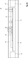
- Fig. 1 comprises Fig. 1A to 1D and shows a schematic cross-sectional side view representation of an exemplary semiconductor device (A), and a few first steps for fabricating the semiconductor device (B to D).
- Fig. 1A shows a semiconductor device 10 which comprises a leadframe based die carrier 11, a semiconductor die 12 disposed on a first upper main face of the die carrier 11, the semiconductor die 12 comprising one or more contact pads 12A (not shown) on a main face thereof, an encapsulant 13 covering the semiconductor die 12 and a portion of the main face of the die carrier 11.
- the semiconductor device 10 further comprises an insulation layer 14 covering the encapsulant 13 and a portion of the first upper main face and a second lower main face of the die carrier 11, and a plurality of electrical interconnects 15 each one being connected with its lower end with one of the contact pads of the semiconductor die 12 and extending through the encapsulant 13 and the insulation layer 14.
- the electrical interconnects 15 are connected with metallic traces which are provided on a metallization layer 16 disposed on top of the insulation layer 14.
- the die carrier 11 is also connected by electrical interconnects 15 with one of the metallic traces 16A. It is alternatively possible that the die carrier 11 is contacted by electrical interconnects reaching via the backside portion of the insulation layer 14.
- the embodiment of a semiconductor device as shown in Fig. 1 is configured such that the die carrier 11 is disposed within an opening portion of a PCB 17 and the insulation layer 14 covers the encapsulant 13 on its upper main face and on its side faces and furthermore reaches through a space between side faces of the die carrier 11 and side faces of the PCB 17 to the backsides of the die carrier 11 and the PCB 17.
- the electrical interconnects 15 not only extend through the encapsulant 13 but also through a portion of the insulation layer 14 which is disposed on the upper surface of the encapsulant 13. As shown in Fig. 1A , there can also be electrical interconnects 15 which only extend through the insulation layer 14, in particular those which connect the die carrier with one of the metallic traces 16A.
- the encapsulant 13 comprises one or more of a resin, an epoxy resin, a polyimide, and a silicone.
- the encapsulant 13 may contain filler materials like filler particles with which the thermal conductivity may be increased. If the encapsulant 13 shall be laser structured, it would be preferable to use rather small filler particles, e.g. in a range from 10 to 50 ⁇ m diameter, so that also vias with small diameters can be laser structured.
- the type of material of the encapsulant 13 can be selected according to the properties of the semiconductor die 12, in particular, the voltage range of the semiconductor die 12. It is therefore possible to employ semiconductor dies with voltages above 100V by choosing an appropriate encapsulant material with sufficient isolation properties.
- the aggregate state of the applied encapsulant can be any one of pellets, granulate, powder, liquid, or a sheet.
- the encapsulant 13 completely covers the upper main face and the side faces of the semiconductor die 12 as is shown in the embodiment of Fig. 1A .
- the encapsulant 13 only partially covers the upper main face of the semiconductor die 12.
- the encapsulant 13 only covers the upper surface of the semiconductor die 12 in the edge regions and possibly the side faces but not in a central region of the upper surface.
- the central region can instead be filled by the insulation layer 14, e.g. laminated by the insulation layer 14.
- the encapsulant 13 can be applied to the edge regions by dispensing, casting, or even an underfill dispensing.
- this embodiment can also be applied in the further embodiments shown and explained in connection with Figs. 2A , 3A , 4A , and 5 .
- the semiconductor die 12 is connected to the die carrier by soldering, in particular diffusion soldering, or sintering, or by the use of glue, in particular a conductive glue like silver glue.
- the semiconductor die 12 can be one or more of vertical transistor die, a MOSFET die, an IGBT die, a SiC-MOS Die, a Cool-MOS die, an S-FET die, a gate driver die, a controller, or a connectivity die configured to connect the semiconductor device to external entities.
- a connectivity die can be, for example, a WiFi module or a USB interface.
- the semiconductor die 12 is one or more of a wide bandgap semiconductor die, a SiC die, or a GaN die.
- a first semiconductor die can be a transistor die, in particular one of the above mentioned transistor dies, and a second semiconductor die can be either a further transistor die or a diode die.
- the transistor dies may function as switches, and two switches can be connected in series or in parallel.
- the insulation layer 14 can be applied in different aggregate states as, for example, in liquid form, as pellets, as a granulate, or as a laminate of any kind of plastic material.
- the insulation layer 14 can be made of a thermally conductive material to allow efficient heat dissipation in particular to the bottom.
- the material of the insulation layer 14 can, in particular, comprise a resin like epoxy resin, and more specifically a material filled with thermally conductive particles like, for example, made of AlO, BNi, AlNi, SiN, diamond, or any other thermally conductive particles.
- the top and bottom layers of the insulation layer 14 can be of different thermal conductivity.
- the bottom layer can have a higher thermal conductivity as heat dissipation to the top is already accomplished by the electrical interconnects. Accordingly the top layer can have a low or even zero amount of filler particles.
- the electrical interconnects 15 can be fabricated by laser drilling through-vias into the encapsulant 13 and possibly also into the insulation layer 14 so that the through-vias reach down to the contact pads 12A of the semiconductor die 12 and thereafter filling an electrically conductive material like e.g. copper into the through-vias.
- the contact pads 12A on the upper surface may be comprised of a source or emitter pad and a gate pad.
- the source pad may be partitioned into a plurality of sub-pads and the electrical interconnects 15 may be connected with these sub-pads.
- the embodiment as shown in Fig. 1A is so configured that the die carrier 11 comprises a planar upper surface and the semiconductor die 12 is disposed on the planar upper surface and further that the encapsulant 13 covers only a portion of the main face of the die carrier 11.
- a thickness of the die carrier 11 can be in a range from 300 ⁇ m to 3 mm, wherein the lower bound of the range can also be 400 or 500 ⁇ m, and the upper bound of the range can also be 2.5 or 2 mm.
- the die carrier 11 can be one of a portion of a leadframe, a direct copper bond (DCB), an active metal braze (AMB), or an isolated metal substrate (IMS).
- DCB direct copper bond
- AMB active metal braze
- IMS isolated metal substrate
- Figs. 1B to 1D illustrate the first steps of fabricating the semiconductor device 10.
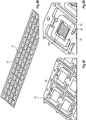
- Fig. 1B shows a perspective view from above onto a leadframe which contains a plurality of die carriers 11 being interconnected within a frame structure.
- a semiconductor die 12 will be disposed and connected to the upper main face of the die carrier 11 by, for example, diffusion soldering.
- Fig. 1C shows an enlarged view onto the left upper portion of the leadframe.
- the semiconductor dies 12 are IBGT dies each comprising on an upper main face thereof the contact pads 12A in the form of a large area source or emitter pad and a small area gate pad. It can be seen in Fig.
- the source pad may be partitioned into a plurality of sub-pads.
- the IGBT dies 12 further comprise a drain pad or collector pad on their back surfaces with which the IGBT dies 12 are connected with the upper surface of the die carriers 11. Thereafter the encapsulant 13 is individually applied onto each one of the IGBT dies 12.
- Fig. 1D shows the same view onto the assembly as Fig. 1C after applying the individual encapsulants 13.
- the encapsulant 13 can be deposited by means of, for example, transfer molding or compression molding, or by lamination.
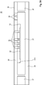
- Fig. 2 comprises Fig. 2A to 2D and shows a schematic cross-sectional side view representation of an exemplary semiconductor device (A), and a few first steps for fabricating the semiconductor module (B to D).
- Fig. 2A shows a semiconductor device 20 comprising a leadframe based die carrier 21, a semiconductor die 22 disposed on a first upper main face of the die carrier 21, the semiconductor die 22 comprising one or more contact pads on a main face thereof, an encapsulant 23 covering the semiconductor die 22, the first upper main face and the side faces of the die carrier 21.
- the semiconductor device 20 further comprises an insulation layer 24 covering the encapsulant 23 and a plurality of electrical interconnects 25 each being connected with one of the contact pads of the semiconductor die 22 and extending through the encapsulant 23.
- a difference of the semiconductor device 20 to the semiconductor device 10 of Fig. 1 is that the encapsulant 23 is covered onto the complete upper main face and also on the side faces of the die carrier 21 and that the electrical interconnects 25 which connect the die carrier 21 with one of the of the metallic traces of the layer 26 extend through both the encapsulant 23 and the insulation layer 24. Accordingly the insulation layer 24 covers the die carrier 11 only on its second lower main face.
- Figs. 2B to 2D illustrate the first steps of fabricating the semiconductor device 20.
- Fig. 2B shows a perspective view from above onto a leadframe which contains a plurality of die carriers 21 being interconnected within a frame structure.
- a semiconductor die 22 Onto each one of the die carriers 21 a semiconductor die 22 will be disposed and connected to the upper main face of the die carrier 21 by, for example, diffusion soldering.
- the encapsulant 23 is applied to the complete structure so that the encapsulant 23 not only covers the entire upper surfaces of the semiconductor devices but also flows into the intermediate spaces between the semiconductor devices of the frame structure and thereby also covers the side faces of the die carriers 21.
- Figs. 2C and 2D show a singulated semiconductor device in a perspective view from below (2C) and in a perspective view from above (2D) where it can be seen that the encapsulant 23 even is covered onto a small edge portion of the lower main face of the die carrier 21.
- the die carrier 21, the semiconductor die 22, the contact pads 22A, the encapsulant 23, the insulation layer 24, the electrical interconnects 25, and the metallization layer 26 of the semiconductor device 20 may otherwise have the same properties as the die carrier 11, the semiconductor die 12, the contact pads 12A, the encapsulant 13, the insulation layer 14, the electrical interconnects 15, the metallization layer 16 of the semiconductor device 10.
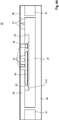
- Fig. 3 comprises Fig. 3A to 3D and shows a schematic cross-sectional side view representation of an exemplary semiconductor (A) and a few first steps for fabricating the semiconductor module (B to D).
- Fig. 3A shows a semiconductor device 30 comprising a leadframe based die carrier 31, which comprises a recessed area 31A in a first upper main face thereof, a semiconductor die 32 disposed in the recessed area 31A, the semiconductor die 32 comprising one or more contact pads on a main face thereof, an encapsulant 33 covering the semiconductor die 32 and the bottom and side faces of the recessed area 31A.
- the semiconductor device 30 further comprises an insulation layer 34 covering the first upper main face, the upper surface of the encapsulant 33 and side faces and a second lower main face of the die carrier 31, and a plurality of electrical interconnects 35 each being connected with one of the contact pads 32A of the semiconductor die 32 and extending through the encapsulant 33.
- the encapsulant 33 can be filled into the recessed area 31A in such a way that its upper surface is coplanar with the upper surface of the die carrier 31.
- a depth of the recessed area 31A can be in a range from 0.2 mm to 2 mm, wherein the lower bound of the range can also be 0.3, 0.4, or 0.5 mm, and the upper bound of the range can also be 1.9, 1.8, 1.7, 1.6, or 1.5 mm and standard values can be 1.27 mm, 1 mm, 0.8 mm, 500 ⁇ m, and 300 ⁇ m.
- the die carrier 31, the semiconductor die 32, the contact pads 32A, the encapsulant 33, the insulation layer 34, the electrical interconnects 35, and the metallization layer 36 of the semiconductor device 30 may otherwise have the same properties as the die carrier 11, the semiconductor die 12, the encapsulant 13, the insulation layer 14, the electrical interconnects 15, and the metallization layer 16 of the semiconductor device 10.
- Figs. 3B to 3D illustrate the first steps of fabricating the semiconductor device 30.
- Fig. 3B shows a perspective view from above onto a leadframe which contains a plurality of die carriers 31 being interconnected within a frame structure, each one of the die carriers 31 comprising a recessed area 31A.
- a semiconductor die 12 will be inserted and connected to the bottom face of the recessed area 31A by, for example, diffusion soldering.
- Fig. 3C shows an enlarged view onto the left upper portion of the leadframe after filling the encapsulant 33 into the recessed areas 31A.
- Fig. 3D shows a perspective view onto the assembly with the encapsulant 33 partly broken away.
- Fig. 4 comprises Fig. 4A to 4D and shows a schematic cross-sectional side view representation of an exemplary semiconductor device (A) and a few first steps for fabricating the semiconductor module (B to D).
- Fig. 4A shows a semiconductor device 40 comprising a leadframe based die carrier 41, which comprises a recessed area 41A in a first upper main face thereof, a semiconductor die 42 disposed in the recessed area 41A, the semiconductor die 42 comprising one or more contact pads 42A (not shown) on a main face thereof, an encapsulant 43 covering the semiconductor die 42 and the bottom and side faces of the recessed area 41A.
- the semiconductor device 40 further comprises an insulation layer 44 covering an upper surface of the encapsulant 43, the first upper main face, the side faces and a second lower main face of the die carrier 41, and first electrical interconnects 45 each being connected with one of the contact pads 42A of the semiconductor die 42 and extending through the encapsulant 43.
- Another way of fabricating the first electrical interconnects 45 is to apply vertical metallic wires to the contact pads before depositing the encapsulant and the insulation layer.
- the vertical wires can extend through an upper surface of the insulation layer.
- a further difference of the semiconductor device 40 to the semiconductor device 30 of Fig. 3 is that the first electrical interconnects 45 only extend through the encapsulant 43 but not through the insulation layer 44. Instead there are provided second electrical interconnects 47 on top of the first interconnects 45. These second interconnects 47 can be fabricated, for example, by drilling through-vias, in particular by a laser, into the insulation layer 44, and then filling the through-vias with a conductive material, in particular copper. The second interconnects 47 can then be connected with particular conductive traces of the metallization layer 46.
- a thickness of the first electrical interconnects 45 can be in a range from 200 ⁇ m to 600 ⁇ m, wherein the lower bound can also be 250 ⁇ m or 300 mm, and the upper bound can also be 550 mm or 500 ⁇ m.
- the encapsulant is 43 filled into the recessed areas 41A. Thereafter it is possible to remove upper protruding portions of the first electrical interconnects 45, in particular if upper surfaces of the first electrical interconnects 45 are not coplanar with an upper surface of the encapsulant 43.
- the removal process of these upper portions of the first electrical interconnects 45 can be performed by, for example, grinding or lasering.
- two or more recessed areas are disposed on the die carrier, wherein similar or different semiconductor dies can be arranged in the recessed areas.
- different encapsulants can be employed for embedding the semiconductor dies according to different requirements as regards, for example, the voltage range of the semiconductor dies.
- Figs. 4B to 4D illustrate the first steps of fabricating the semiconductor device 40.
- Fig. 4B shows a perspective view from above onto a single die carrier 41 which comprises a recessed area 41A.
- a semiconductor die 42 will be inserted and connected to the bottom face of the recessed area 41A by, for example, diffusion soldering.
- Fig. 4C shows a perspective view after placing first electrical interconnects 45 onto the contact pads 42A of the semiconductor die 42 by, for example, one of the above described methods.
- the first electrical interconnects 45 can be applied in such a way that their upper surfaces are coplanar with the upper surface of the die carrier 41.
- FIG. 4D shows a perspective view after filling the encapsulant 43 into the recessed area 41A.
- the encapsulant 43 can be filled into the recessed area 41A in such a way that its upper surface is coplanar with the upper surface of the die carrier 41 and the upper surfaces of the first electrical interconnects 45 are exposed to the outside.
- the die carrier 41, the semiconductor die 42, the contact pads 42A, the encapsulant 43, the insulation layer 44, the first electrical interconnects 45, and the metallization layer 46 of the semiconductor device 40 may otherwise have the same properties as the die carrier 11, the semiconductor die 12, the contact pads 12A, the encapsulant 13, the insulation layer 14, the electrical interconnects 15, and the metallization layer 16 of the semiconductor device 10.
- Fig. 5 shows a schematic cross-sectional side view representation of an exemplary semiconductor device according to the first aspect.
- Fig. 5 shows a semiconductor device 50 which comprises a leadframe based die carrier 51, a semiconductor die 52 disposed on a first upper main face of the die carrier 51, the semiconductor die 52 comprising one or more contact pads on a main face thereof, an encapsulant 53 covering the semiconductor die 52 and at least a portion of the main face of the die carrier 51.
- the semiconductor device 50 further comprises an insulation layer 54 covering the encapsulant 53 and a portion of the first upper main face and a second lower main of the die carrier 51, and a plurality of first electrical interconnects 55 each one being connected with its lower end with one of the contact pads of the semiconductor die 52 and extending through the encapsulant 53.
- the semiconductor device 50 further comprises a plurality of second interconnects 57 each one being connected with its lower end with one of the first electrical interconnects 55. At their upper ends the second electrical interconnects 57 are connected with metallic traces 56.
- the die carrier 51 is also connected by second electrical interconnects 57 with one of the metallic traces 66. Again here it is alternatively possible that the die carrier 51 is contacted by electrical interconnects reaching via the backside portion of the insulation layer 54.
- first and second electrical interconnects 55 and 57 can be fabricated by forming vias by laser structuring into the encapsulant 53 and the insulation layer 54 followed by galvanic depositing or chemical plating or sputtering or printing a metal, in particular copper, into the vias. Furthermore the electrical interconnects 55 and 57 need not be arranged one above the other. As shown in the embodiment of Fig. 5 , there can be a lateral displacement between them and a redistribution layer comprising metallic lines laterally connecting the ends of the electrical interconnects 55 and 57 with each other.
- the die carrier 51, the semiconductor die 52, the encapsulant 53, the insulation layer 54, the electrical interconnects 55, and the metallization layer 56 of the semiconductor device 50 may otherwise have the same properties as the die carrier 11, the semiconductor die 12, the contact pads 12A, the encapsulant 13, the insulation layer 14, the electrical interconnects 15, and the metallization layer 16 of the semiconductor device 10.
- the electrical interconnects or at least part of the electrical interconnects can be fabricated by chemical plating, in particular electroplating or galvanic plating, or sputtering or printing. Interconnects formed in this way are known to be superior over all other types of electrical contacts. With this it becomes possible to fabricate semiconductor devices of high reliability and robustness.
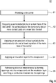
- Fig. 6 shows a flow diagram of an exemplary method for fabricating a semiconductor device in which method the electrical interconnects are fabricated after applying the encapsulant and the insulation layer.
- the method 60 of Fig. 6 comprises providing a die carrier (61), disposing a semiconductor die on a main face of the die carrier, the semiconductor die comprising one or more contact pads on a main face thereof (62), applying an encapsulant at least partially to the semiconductor die and at least a portion of the main face of the die carrier (63), applying an insulation layer to the encapsulant (64), and fabricating electrical interconnects by forming openings into the encapsulant and the insulation layer and filling a conductive material into the openings (65).
- a die carrier 31 which comprises a recessed area 31A.
- Fig. 7 shows a flow diagram of an exemplary method for fabricating a semiconductor device in which method the electrical interconnects are fabricated before applying the encapsulant and the insulation layer.
- the method 70 of Fig. 7 comprises providing a die carrier (71), disposing a semiconductor die on a main face of the die carrier, the semiconductor die comprising one or more contact pads on a main face thereof (72), disposing first electrical interconnects on the one or more contact pads of the semiconductor die (73), applying an encapsulant at least partially to the semiconductor die and at least a portion of the main face of the die carrier (74), applying an insulation layer to the encapsulant (75), and fabricating second electrical interconnects by forming openings into the insulation layer and filling a conductive material into the openings (76).
- a semiconductor device as shown in Fig. 4 can be fabricated.
- a die carrier 41 is provided which comprises a recessed area 41A.
- the first electrical interconnects are shown with reference sign 45, and the second electrical interconnects are shown with reference sign 47.
- the openings are formed into either both the encapsulant and the insulation layer (method 60) or only into the insulation layer (method 70) by laser drilling.
- the electrical interconnects are fabricated by one of pre-fabricating metallic blocks or wires and then applying the blocks or wires to the one or more contact pads, or by cold spraying.
- the semiconductor die can be tested for functionality.
- the semiconductor die can, in particular, be tested before applying the encapsulant and the insulation layer. It can, however also be tested after applying the encapsulant and the insulation layer, in particular in case the electrical interconnects extending through an upper surface of the insulation layer.
- Further embodiments of the method 60 can be formed by adding aspects or features which were described above in connection with the semiconductor device according to the first aspect.
Landscapes
- Structures Or Materials For Encapsulating Or Coating Semiconductor Devices Or Solid State Devices (AREA)
Abstract
The semiconductor device (10) comprises a die carrier (11), a semiconductor die (12) disposed on a main face of the die carrier (11), the semiconductor die (12) comprising one or more contact pads (12A) on a main face thereof, an encapsulant (13) covering at least partially the semiconductor die (12) and at least a portion of the main face of the die carrier (11), and an insulation layer (14) covering the encapsulant (13), and one or more electrical interconnects (15), each being connected with one of the contact pads (12A) of the semiconductor die (12) and extending through the encapsulant (13).
Description
- The present disclosure is related in general to semiconductor devices, in particular to semiconductor power devices. The present disclosure is in particular related to a semiconductor device comprising an embedded semiconductor die disposed on a leadframe based die carrier and a method for fabricating such a semiconductor device.
- Chip embedding is a solution where an active or passive component is positioned in between at least two layers of a printed circuit board. Today it is commonly used for low voltage signal processing systems, there are first attempts to apply embedding for power circuits with low voltages <100V, but for high voltages special challenges are to be expected in connection with the high electric fields. The motivations for doing that are manifold, e.g. increasing power density, extreme low parasitic inductances, better EMI shielding, and also high reliability and high power cycling robustness. Also chip embedding usually employs chemically plated, in particular electroplated, electrical interconnects, which are superior over other types of electrical interconnects.
- A solution for manufacturing a chip embedded high voltage semiconductor device is to place the die on a leadframe, singulate the dies on leadframe and embed this assembly afterwards. One risk of the embedding technology is the interaction of the devices with the used carrier material where one dominant mechanism among other things is the voltage and the resulting electric field. This can lead in worst case to a destruction of the assembly caused by e.g. copper migration. Another threat is the exposed copper metallization on the die. Oxidation of this must be treated special in the embedding process. After the placement of the component, the connection to the outer layers is done through vias. Especially the passage from the via to the die metallization is a critical point for cracks. In addition there is a strong interaction of the embedding encapsulation material and the fabrication process in combination with high voltage devices and resulting electric field, causing chemical degradation of encapsulation material (e.g. pentode, reversible drifts), voltage drift of the device by ions from encapsulation material, corrosion of the device. Embedding material is also sensible to humidity and cannot guarantee density to the covered chips which accelerates the negative effects just described. To prevent delamination of the surrounding layers cavities in the leadframe are used, where the die is placed afterwards. Following this approach for each die a dedicated cavity must be done.
- A first aspect of the present disclosure is related to a semiconductor device comprising a die carrier, a semiconductor die disposed on the die carrier, the semiconductor die comprising one or more contact pads on a main face thereof, an encapsulant covering at least partially the semiconductor die and at least a portion of the main face of the die carrier, and an insulation layer covering the encapsulant, and one or more electrical interconnects each being connected with one of the contact pads of the semiconductor die and extending through the encapsulant.
- A second aspect of the present disclosure is related to a method for fabricating a semiconductor device, the method comprising providing a die carrier, disposing a semiconductor die on a main face of the die carrier, the semiconductor die comprising one or more contact pads on a main face thereof, applying an encapsulant at least partially to the semiconductor die and at least a portion of the main face of the die carrier, , applying an insulation layer to the encapsulant; and fabricating electrical interconnects by forming openings into the encapsulant and the insulation layer and filling a conductive material into the openings.
- A third aspect of the present disclosure is related to a method for fabricating a semiconductor device, the method comprising providing a die carrier, disposing a semiconductor die on a main face of the die carrier, the semiconductor die comprising one or more contact pads on a main face thereof, disposing first electrical interconnects on the one or more contact pads of the semiconductor die, applying an encapsulant at least partially to the semiconductor die and at least a portion of the main face of the die carrier, applying an insulation layer to the encapsulant, and fabricating second electrical interconnects by forming openings into the insulation layer and filling a conductive material into the openings.
- The accompanying drawings are included to provide a further understanding of embodiments and are incorporated in and constitute a part of this specification. The drawings illustrate embodiments and together with the description serve to explain principles of embodiments. Other embodiments and many of the intended advantages of embodiments will be readily appreciated as they become better understood by reference to the following detailed description.
- The elements of the drawings are not necessarily to scale relative to each other. Like reference numerals designate corresponding similar parts.
-
Fig. 1 comprisesFig. 1A to 1D and shows a schematic cross-sectional side view representation of an exemplary semiconductor device according to the first aspect, wherein the die carrier comprises a planar upper surface and the semiconductor die is disposed on the upper planar surface, and the encapsulant is disposed on the semiconductor die and only a portion of the upper planar surface of the die carrier (A), and a few first steps for fabricating the semiconductor device (B to D) . -
Fig. 2 comprisesFig. 2A to 2D and shows a schematic cross-sectional side view representation of an exemplary semiconductor device according to the first aspect, wherein the die carrier comprises a planar upper surface and the semiconductor die is disposed on the upper planar surface, and the encapsulant is disposed on the semiconductor die and on the complete upper planar surface and on the side faces of the die carrier (A), and a few first steps for fabricating the semiconductor module (B to D). -
Fig. 3 comprisesFig. 3A to 3D and shows a schematic cross-sectional side view representation of an exemplary semiconductor device according to the first aspect, wherein the die carrier comprises a recessed area and the semiconductor die is disposed in the recessed area, and the encapsulant is disposed in the recessed area on the semiconductor die and a plurality of electrical through-connections is formed in the encapsulant (A) and a few first steps for fabricating the semiconductor module (B to D). -
Fig. 4 comprisesFig. 4A to 4D and shows a schematic cross-sectional side view representation of an exemplary semiconductor device according to the first aspect, wherein the die carrier comprises a recessed area and the semiconductor die is disposed in the recced area, and large area electrical interconnects are provided which reach through the encapsulant (A) and a few first steps for fabricating the semiconductor module (B to D). -
Fig. 5 shows a schematic cross-sectional side view representation of an exemplary semiconductor device according to the first aspect, wherein two types of electrical interconnects are provided wherein one type of them reach through the encapsulant and the other type of them reach through the insulation layer. -
Fig. 6 shows a flow diagram of an exemplary method for fabricating a semiconductor device, wherein the electrical interconnects are fabricated after applying the encapsulant and the insulation layer. -
Fig. 7 shows a flow diagram of an exemplary method for fabricating a semiconductor device, wherein the electrical interconnects are fabricated before applying the encapsulant and the insulation layer. - In the following detailed description, reference is made to the accompanying drawings, which form a part hereof, and in which is shown by way of illustration specific embodiments in which the disclosure may be practiced. In this regard, directional terminology, such as "top", "bottom", "front", "back", "leading", "trailing", etc., is used with reference to the orientation of the Figure(s) being described. Because components of embodiments can be positioned in a number of different orientations, the directional terminology is used for purposes of illustration and is in no way limiting. It is to be understood that other embodiments may be utilized and structural or logical changes may be made without departing from the scope of the present disclosure. The following detailed description, therefore, is not to be taken in a limiting sense, and the scope of the present disclosure is defined by the appended claims.
- It is to be understood that the features of the various exemplary embodiments described herein may be combined with each other, unless specifically noted otherwise.
- As employed in this specification, the terms "bonded", "attached", "connected", "coupled" and/or "electrically connected/electrically coupled" are not meant to mean that the elements or layers must directly be contacted together; intervening elements or layers may be provided between the "bonded", "attached", "connected", "coupled" and/or "electrically connected/electrically coupled" elements, respectively. However, in accordance with the disclosure, the above-mentioned terms may, optionally, also have the specific meaning that the elements or layers are directly contacted together, i.e. that no intervening elements or layers are provided between the "bonded", "attached", "connected", "coupled" and/or "electrically connected/electrically coupled" elements, respectively.
- Further, the word "over" used with regard to a part, element or material layer formed or located "over" a surface may be used herein to mean that the part, element or material layer be located (e.g. placed, formed, deposited, etc.) "indirectly on" the implied surface with one or more additional parts, elements or layers being arranged between the implied surface and the part, element or material layer. However, the word "over" used with regard to a part, element or material layer formed or located "over" a surface may, optionally, also have the specific meaning that the part, element or material layer be located (e.g. placed, formed, deposited, etc.) "directly on", e.g. in direct contact with, the implied surface.
-
Fig. 1 comprisesFig. 1A to 1D and shows a schematic cross-sectional side view representation of an exemplary semiconductor device (A), and a few first steps for fabricating the semiconductor device (B to D). -
Fig. 1A shows asemiconductor device 10 which comprises a leadframe baseddie carrier 11, asemiconductor die 12 disposed on a first upper main face of the diecarrier 11, the semiconductor die 12 comprising one ormore contact pads 12A (not shown) on a main face thereof, anencapsulant 13 covering the semiconductor die 12 and a portion of the main face of the diecarrier 11. Thesemiconductor device 10 further comprises aninsulation layer 14 covering theencapsulant 13 and a portion of the first upper main face and a second lower main face of thedie carrier 11, and a plurality ofelectrical interconnects 15 each one being connected with its lower end with one of the contact pads of thesemiconductor die 12 and extending through theencapsulant 13 and theinsulation layer 14. At their upper ends theelectrical interconnects 15 are connected with metallic traces which are provided on ametallization layer 16 disposed on top of theinsulation layer 14. The diecarrier 11 is also connected byelectrical interconnects 15 with one of the metallic traces 16A. It is alternatively possible that thedie carrier 11 is contacted by electrical interconnects reaching via the backside portion of theinsulation layer 14. - The embodiment of a semiconductor device as shown in
Fig. 1 is configured such that thedie carrier 11 is disposed within an opening portion of aPCB 17 and theinsulation layer 14 covers theencapsulant 13 on its upper main face and on its side faces and furthermore reaches through a space between side faces of thedie carrier 11 and side faces of thePCB 17 to the backsides of thedie carrier 11 and thePCB 17. Theelectrical interconnects 15 not only extend through theencapsulant 13 but also through a portion of theinsulation layer 14 which is disposed on the upper surface of theencapsulant 13. As shown inFig. 1A , there can also beelectrical interconnects 15 which only extend through theinsulation layer 14, in particular those which connect the die carrier with one of the metallic traces 16A. - According to an embodiment of the semiconductor device of
Fig. 1 , theencapsulant 13 comprises one or more of a resin, an epoxy resin, a polyimide, and a silicone. Theencapsulant 13 may contain filler materials like filler particles with which the thermal conductivity may be increased. If theencapsulant 13 shall be laser structured, it would be preferable to use rather small filler particles, e.g. in a range from 10 to 50 µm diameter, so that also vias with small diameters can be laser structured. In particular, the type of material of theencapsulant 13 can be selected according to the properties of the semiconductor die 12, in particular, the voltage range of the semiconductor die 12. It is therefore possible to employ semiconductor dies with voltages above 100V by choosing an appropriate encapsulant material with sufficient isolation properties. The aggregate state of the applied encapsulant can be any one of pellets, granulate, powder, liquid, or a sheet. - According to an embodiment of the semiconductor device according to the first aspect, the
encapsulant 13 completely covers the upper main face and the side faces of the semiconductor die 12 as is shown in the embodiment ofFig. 1A . - According to another embodiment of the semiconductor device according to the first aspect, the
encapsulant 13 only partially covers the upper main face of the semiconductor die 12. In particular, it is possible that for reasons of edge termination and avoidance of high electric fields the encapsulant 13 only covers the upper surface of the semiconductor die 12 in the edge regions and possibly the side faces but not in a central region of the upper surface. The central region can instead be filled by theinsulation layer 14, e.g. laminated by theinsulation layer 14. Moreover, in such an embodiment theencapsulant 13 can be applied to the edge regions by dispensing, casting, or even an underfill dispensing. Furthermore it should be noted that this embodiment can also be applied in the further embodiments shown and explained in connection withFigs. 2A ,3A ,4A , and5 . - According to an embodiment of the semiconductor device of
Fig. 1 , the semiconductor die 12 is connected to the die carrier by soldering, in particular diffusion soldering, or sintering, or by the use of glue, in particular a conductive glue like silver glue. - According to an embodiment of the semiconductor device of
Fig. 1 , the semiconductor die 12 can be one or more of vertical transistor die, a MOSFET die, an IGBT die, a SiC-MOS Die, a Cool-MOS die, an S-FET die, a gate driver die, a controller, or a connectivity die configured to connect the semiconductor device to external entities. A connectivity die can be, for example, a WiFi module or a USB interface. - According to an embodiment of the semiconductor device of
Fig. 1 , the semiconductor die 12 is one or more of a wide bandgap semiconductor die, a SiC die, or a GaN die. - According to an embodiment of the semiconductor device of
Fig. 1 , two or more semiconductor dies are disposed on thedie carrier 11. For example, a first semiconductor die can be a transistor die, in particular one of the above mentioned transistor dies, and a second semiconductor die can be either a further transistor die or a diode die. The transistor dies may function as switches, and two switches can be connected in series or in parallel. - According to an embodiment of the semiconductor device of
Fig. 1 , theinsulation layer 14 can be applied in different aggregate states as, for example, in liquid form, as pellets, as a granulate, or as a laminate of any kind of plastic material. Moreover, theinsulation layer 14 can be made of a thermally conductive material to allow efficient heat dissipation in particular to the bottom. The material of theinsulation layer 14 can, in particular, comprise a resin like epoxy resin, and more specifically a material filled with thermally conductive particles like, for example, made of AlO, BNi, AlNi, SiN, diamond, or any other thermally conductive particles. Also the top and bottom layers of theinsulation layer 14 can be of different thermal conductivity. In particular, the bottom layer can have a higher thermal conductivity as heat dissipation to the top is already accomplished by the electrical interconnects. Accordingly the top layer can have a low or even zero amount of filler particles. - According to an embodiment of the
semiconductor device 10, theelectrical interconnects 15 can be fabricated by laser drilling through-vias into theencapsulant 13 and possibly also into theinsulation layer 14 so that the through-vias reach down to thecontact pads 12A of the semiconductor die 12 and thereafter filling an electrically conductive material like e.g. copper into the through-vias. In case of an IGBT die 12 thecontact pads 12A on the upper surface may be comprised of a source or emitter pad and a gate pad. The source pad may be partitioned into a plurality of sub-pads and theelectrical interconnects 15 may be connected with these sub-pads. - The embodiment as shown in
Fig. 1A is so configured that thedie carrier 11 comprises a planar upper surface and the semiconductor die 12 is disposed on the planar upper surface and further that theencapsulant 13 covers only a portion of the main face of thedie carrier 11. - According to an embodiment of the
semiconductor device 10, a thickness of thedie carrier 11 can be in a range from 300 µm to 3 mm, wherein the lower bound of the range can also be 400 or 500 µm, and the upper bound of the range can also be 2.5 or 2 mm. - According to an embodiment of the
semiconductor device 10, thedie carrier 11 can be one of a portion of a leadframe, a direct copper bond (DCB), an active metal braze (AMB), or an isolated metal substrate (IMS). -
Figs. 1B to 1D illustrate the first steps of fabricating thesemiconductor device 10.Fig. 1B shows a perspective view from above onto a leadframe which contains a plurality ofdie carriers 11 being interconnected within a frame structure. Onto each one of the die carriers 11 asemiconductor die 12 will be disposed and connected to the upper main face of thedie carrier 11 by, for example, diffusion soldering.Fig. 1C shows an enlarged view onto the left upper portion of the leadframe. In the present embodiment the semiconductor dies 12 are IBGT dies each comprising on an upper main face thereof thecontact pads 12A in the form of a large area source or emitter pad and a small area gate pad. It can be seen inFig. 1C that the source pad may be partitioned into a plurality of sub-pads. The IGBT dies 12 further comprise a drain pad or collector pad on their back surfaces with which the IGBT dies 12 are connected with the upper surface of thedie carriers 11. Thereafter theencapsulant 13 is individually applied onto each one of the IGBT dies 12.Fig. 1D shows the same view onto the assembly asFig. 1C after applying theindividual encapsulants 13. - The
encapsulant 13 can be deposited by means of, for example, transfer molding or compression molding, or by lamination. -
Fig. 2 comprisesFig. 2A to 2D and shows a schematic cross-sectional side view representation of an exemplary semiconductor device (A), and a few first steps for fabricating the semiconductor module (B to D). -
Fig. 2A shows asemiconductor device 20 comprising a leadframe baseddie carrier 21, asemiconductor die 22 disposed on a first upper main face of thedie carrier 21, the semiconductor die 22 comprising one or more contact pads on a main face thereof, anencapsulant 23 covering the semiconductor die 22, the first upper main face and the side faces of thedie carrier 21. Thesemiconductor device 20 further comprises aninsulation layer 24 covering theencapsulant 23 and a plurality ofelectrical interconnects 25 each being connected with one of the contact pads of the semiconductor die 22 and extending through theencapsulant 23. - A difference of the
semiconductor device 20 to thesemiconductor device 10 ofFig. 1 is that theencapsulant 23 is covered onto the complete upper main face and also on the side faces of thedie carrier 21 and that theelectrical interconnects 25 which connect thedie carrier 21 with one of the of the metallic traces of thelayer 26 extend through both theencapsulant 23 and theinsulation layer 24. Accordingly theinsulation layer 24 covers thedie carrier 11 only on its second lower main face. -
Figs. 2B to 2D illustrate the first steps of fabricating thesemiconductor device 20.Fig. 2B shows a perspective view from above onto a leadframe which contains a plurality ofdie carriers 21 being interconnected within a frame structure. Onto each one of the die carriers 21 asemiconductor die 22 will be disposed and connected to the upper main face of thedie carrier 21 by, for example, diffusion soldering. As illustrated inFig. 2B , in contrast to the method as shown inFigs. 1B to 1D , in this embodiment theencapsulant 23 is applied to the complete structure so that theencapsulant 23 not only covers the entire upper surfaces of the semiconductor devices but also flows into the intermediate spaces between the semiconductor devices of the frame structure and thereby also covers the side faces of thedie carriers 21.Figs. 2C and 2D show a singulated semiconductor device in a perspective view from below (2C) and in a perspective view from above (2D) where it can be seen that theencapsulant 23 even is covered onto a small edge portion of the lower main face of thedie carrier 21. - The
die carrier 21, the semiconductor die 22, thecontact pads 22A, theencapsulant 23, theinsulation layer 24, theelectrical interconnects 25, and themetallization layer 26 of thesemiconductor device 20 may otherwise have the same properties as thedie carrier 11, the semiconductor die 12, thecontact pads 12A, theencapsulant 13, theinsulation layer 14, theelectrical interconnects 15, themetallization layer 16 of thesemiconductor device 10. -
Fig. 3 comprisesFig. 3A to 3D and shows a schematic cross-sectional side view representation of an exemplary semiconductor (A) and a few first steps for fabricating the semiconductor module (B to D). -
Fig. 3A shows asemiconductor device 30 comprising a leadframe baseddie carrier 31, which comprises a recessedarea 31A in a first upper main face thereof, asemiconductor die 32 disposed in the recessedarea 31A, the semiconductor die 32 comprising one or more contact pads on a main face thereof, anencapsulant 33 covering the semiconductor die 32 and the bottom and side faces of the recessedarea 31A. Thesemiconductor device 30 further comprises aninsulation layer 34 covering the first upper main face, the upper surface of theencapsulant 33 and side faces and a second lower main face of thedie carrier 31, and a plurality ofelectrical interconnects 35 each being connected with one of thecontact pads 32A of the semiconductor die 32 and extending through theencapsulant 33. - As shown in the embodiment of
Fig. 3A , theencapsulant 33 can be filled into the recessedarea 31A in such a way that its upper surface is coplanar with the upper surface of thedie carrier 31. - According to an embodiment of the semiconductor device of
Fig. 3 , a depth of the recessedarea 31A can be in a range from 0.2 mm to 2 mm, wherein the lower bound of the range can also be 0.3, 0.4, or 0.5 mm, and the upper bound of the range can also be 1.9, 1.8, 1.7, 1.6, or 1.5 mm and standard values can be 1.27 mm, 1 mm, 0.8 mm, 500 µm, and 300 µm. - The
die carrier 31, the semiconductor die 32, thecontact pads 32A, theencapsulant 33, theinsulation layer 34, theelectrical interconnects 35, and themetallization layer 36 of thesemiconductor device 30 may otherwise have the same properties as thedie carrier 11, the semiconductor die 12, theencapsulant 13, theinsulation layer 14, theelectrical interconnects 15, and themetallization layer 16 of thesemiconductor device 10. -
Figs. 3B to 3D illustrate the first steps of fabricating thesemiconductor device 30.Fig. 3B shows a perspective view from above onto a leadframe which contains a plurality ofdie carriers 31 being interconnected within a frame structure, each one of thedie carriers 31 comprising a recessedarea 31A. Into each one of the recessedareas 31A of the die carriers 31 asemiconductor die 12 will be inserted and connected to the bottom face of the recessedarea 31A by, for example, diffusion soldering.Fig. 3C shows an enlarged view onto the left upper portion of the leadframe after filling theencapsulant 33 into the recessedareas 31A.Fig. 3D shows a perspective view onto the assembly with theencapsulant 33 partly broken away. -
Fig. 4 comprisesFig. 4A to 4D and shows a schematic cross-sectional side view representation of an exemplary semiconductor device (A) and a few first steps for fabricating the semiconductor module (B to D). -
Fig. 4A shows asemiconductor device 40 comprising a leadframe baseddie carrier 41, which comprises a recessedarea 41A in a first upper main face thereof, asemiconductor die 42 disposed in the recessedarea 41A, the semiconductor die 42 comprising one ormore contact pads 42A (not shown) on a main face thereof, anencapsulant 43 covering the semiconductor die 42 and the bottom and side faces of the recessedarea 41A. Thesemiconductor device 40 further comprises aninsulation layer 44 covering an upper surface of theencapsulant 43, the first upper main face, the side faces and a second lower main face of thedie carrier 41, and firstelectrical interconnects 45 each being connected with one of thecontact pads 42A of the semiconductor die 42 and extending through theencapsulant 43. - A difference of the
semiconductor device 40 to thesemiconductor device 30 ofFig. 3 is that the firstelectrical interconnects 45 are formed in a different manner. More specifically, the firstelectrical interconnects 45 are applied in the form of massive contiguous blocks of a metallic material to thecontact pads 42A of the semiconductor die 42. This can be done in different ways. One way is to prefabricate the metallic blocks as e.g. copper blocks and then the blocks can be applied to thecontact pads 42A as a whole by, for example, adhering by use of a glue like silver glue. Another way of fabricating the firstelectrical interconnects 45 is to employ a gas dynamic cold spraying or cold spraying method wherein solid metal powders are accelerated in a supersonic jet to velocities up to ca. 1200 m/s. During impact with the substrate, particles undergo plastic deformation and adhere to the surface. To achieve a uniform thickness the spraying nozzle can be scanned along the substrate. Another way of fabricating the firstelectrical interconnects 45 is to apply vertical metallic wires to the contact pads before depositing the encapsulant and the insulation layer. In particular, the vertical wires can extend through an upper surface of the insulation layer. - A further difference of the
semiconductor device 40 to thesemiconductor device 30 ofFig. 3 is that the firstelectrical interconnects 45 only extend through theencapsulant 43 but not through theinsulation layer 44. Instead there are provided secondelectrical interconnects 47 on top of thefirst interconnects 45. These second interconnects 47 can be fabricated, for example, by drilling through-vias, in particular by a laser, into theinsulation layer 44, and then filling the through-vias with a conductive material, in particular copper. The second interconnects 47 can then be connected with particular conductive traces of themetallization layer 46. - A thickness of the first
electrical interconnects 45 can be in a range from 200 µm to 600 µm, wherein the lower bound can also be 250 µm or 300 mm, and the upper bound can also be 550 mm or 500 µm. - After fabricating the first
electrical interconnects 45 in the above described manner, the encapsulant is 43 filled into the recessedareas 41A. Thereafter it is possible to remove upper protruding portions of the firstelectrical interconnects 45, in particular if upper surfaces of the firstelectrical interconnects 45 are not coplanar with an upper surface of theencapsulant 43. The removal process of these upper portions of the firstelectrical interconnects 45 can be performed by, for example, grinding or lasering. - According to an embodiment of the
semiconductor devices -
Figs. 4B to 4D illustrate the first steps of fabricating thesemiconductor device 40.Fig. 4B shows a perspective view from above onto asingle die carrier 41 which comprises a recessedarea 41A. Into the recessedarea 41A of the die carrier 41 asemiconductor die 42 will be inserted and connected to the bottom face of the recessedarea 41A by, for example, diffusion soldering.Fig. 4C shows a perspective view after placing firstelectrical interconnects 45 onto thecontact pads 42A of the semiconductor die 42 by, for example, one of the above described methods. The firstelectrical interconnects 45 can be applied in such a way that their upper surfaces are coplanar with the upper surface of thedie carrier 41.Fig. 4D shows a perspective view after filling theencapsulant 43 into the recessedarea 41A. Theencapsulant 43 can be filled into the recessedarea 41A in such a way that its upper surface is coplanar with the upper surface of thedie carrier 41 and the upper surfaces of the firstelectrical interconnects 45 are exposed to the outside. - The
die carrier 41, the semiconductor die 42, thecontact pads 42A, theencapsulant 43, theinsulation layer 44, the firstelectrical interconnects 45, and themetallization layer 46 of thesemiconductor device 40 may otherwise have the same properties as thedie carrier 11, the semiconductor die 12, thecontact pads 12A, theencapsulant 13, theinsulation layer 14, theelectrical interconnects 15, and themetallization layer 16 of thesemiconductor device 10. -
Fig. 5 shows a schematic cross-sectional side view representation of an exemplary semiconductor device according to the first aspect. -
Fig. 5 shows asemiconductor device 50 which comprises a leadframe baseddie carrier 51, asemiconductor die 52 disposed on a first upper main face of thedie carrier 51, the semiconductor die 52 comprising one or more contact pads on a main face thereof, an encapsulant 53 covering the semiconductor die 52 and at least a portion of the main face of thedie carrier 51. Thesemiconductor device 50 further comprises aninsulation layer 54 covering the encapsulant 53 and a portion of the first upper main face and a second lower main of thedie carrier 51, and a plurality of firstelectrical interconnects 55 each one being connected with its lower end with one of the contact pads of the semiconductor die 52 and extending through the encapsulant 53. Thesemiconductor device 50 further comprises a plurality ofsecond interconnects 57 each one being connected with its lower end with one of the firstelectrical interconnects 55. At their upper ends the secondelectrical interconnects 57 are connected with metallic traces 56. Thedie carrier 51 is also connected by secondelectrical interconnects 57 with one of the metallic traces 66. Again here it is alternatively possible that thedie carrier 51 is contacted by electrical interconnects reaching via the backside portion of theinsulation layer 54. - It should be mentioned that the first and second
electrical interconnects insulation layer 54 followed by galvanic depositing or chemical plating or sputtering or printing a metal, in particular copper, into the vias. Furthermore theelectrical interconnects Fig. 5 , there can be a lateral displacement between them and a redistribution layer comprising metallic lines laterally connecting the ends of theelectrical interconnects - The
die carrier 51, the semiconductor die 52, the encapsulant 53, theinsulation layer 54, theelectrical interconnects 55, and themetallization layer 56 of thesemiconductor device 50 may otherwise have the same properties as thedie carrier 11, the semiconductor die 12, thecontact pads 12A, theencapsulant 13, theinsulation layer 14, theelectrical interconnects 15, and themetallization layer 16 of thesemiconductor device 10. - One great advantage of the present disclosure is that throughout all the above described embodiments the electrical interconnects or at least part of the electrical interconnects can be fabricated by chemical plating, in particular electroplating or galvanic plating, or sputtering or printing. Interconnects formed in this way are known to be superior over all other types of electrical contacts. With this it becomes possible to fabricate semiconductor devices of high reliability and robustness.
-
Fig. 6 shows a flow diagram of an exemplary method for fabricating a semiconductor device in which method the electrical interconnects are fabricated after applying the encapsulant and the insulation layer. - The
method 60 ofFig. 6 comprises providing a die carrier (61), disposing a semiconductor die on a main face of the die carrier, the semiconductor die comprising one or more contact pads on a main face thereof (62), applying an encapsulant at least partially to the semiconductor die and at least a portion of the main face of the die carrier (63), applying an insulation layer to the encapsulant (64), and fabricating electrical interconnects by forming openings into the encapsulant and the insulation layer and filling a conductive material into the openings (65). - With the
method 60 ofFig. 6 , for example, semiconductor devices as shown inFigs. 1 to 3 can be fabricated. In case of thesemiconductor 30 as shown inFig. 3 adie carrier 31 is provided which comprises a recessedarea 31A. -
Fig. 7 shows a flow diagram of an exemplary method for fabricating a semiconductor device in which method the electrical interconnects are fabricated before applying the encapsulant and the insulation layer. - The
method 70 ofFig. 7 comprises providing a die carrier (71), disposing a semiconductor die on a main face of the die carrier, the semiconductor die comprising one or more contact pads on a main face thereof (72), disposing first electrical interconnects on the one or more contact pads of the semiconductor die (73), applying an encapsulant at least partially to the semiconductor die and at least a portion of the main face of the die carrier (74), applying an insulation layer to the encapsulant (75), and fabricating second electrical interconnects by forming openings into the insulation layer and filling a conductive material into the openings (76). - With the
method 70 ofFig. 7 , for example, a semiconductor device as shown inFig. 4 can be fabricated. In this case of thesemiconductor device 40 as shown inFig. 4 adie carrier 41 is provided which comprises a recessedarea 41A. The first electrical interconnects are shown withreference sign 45, and the second electrical interconnects are shown withreference sign 47. - According to an embodiment of the
methods - According to an embodiment of the
method 70, the electrical interconnects are fabricated by one of pre-fabricating metallic blocks or wires and then applying the blocks or wires to the one or more contact pads, or by cold spraying. - According to an embodiment of the
methods - Further embodiments of the
method 60 can be formed by adding aspects or features which were described above in connection with the semiconductor device according to the first aspect. - In addition, while a particular feature or aspect of an embodiment of the disclosure may have been disclosed with respect to only one of several implementations, such feature or aspect may be combined with one or more other features or aspects of the other implementations as may be desired and advantageous for any given or particular application. Furthermore, to the extent that the terms "include", "have", "with", or other variants thereof are used in either the detailed description or the claims, such terms are intended to be inclusive in a manner similar to the term "comprise". Furthermore, it should be understood that embodiments of the disclosure may be implemented in discrete circuits, partially integrated circuits or fully integrated circuits or programming means. Also, the term "exemplary" is merely meant as an example, rather than the best or optimal. It is also to be appreciated that features and/or elements depicted herein are illustrated with particular dimensions relative to one another for purposes of simplicity and ease of understanding, and that actual dimensions may differ substantially from that illustrated herein.
- Although specific embodiments have been illustrated and described herein, it will be appreciated by those of ordinary skill in the art that a variety of alternate and/or equivalent implementations may be substituted for the specific embodiments shown and described without departing from the scope of the present disclosure. This application is intended to cover any adaptations or variations of the specific embodiments discussed herein. Therefore, it is intended that this disclosure be limited only by the claims and the equivalents thereof.
Claims (15)
- A semiconductor device (10), comprising:- a die carrier (11);- a semiconductor die (12) disposed on the die carrier (11), the semiconductor die (12) comprising one or more contact pads on a main face thereof;- an encapsulant (13) covering at least partially the semiconductor die (12) and at least a portion of the main face of the die carrier (11),- an insulation layer (14) covering the encapsulant (13); and- one or more electrical interconnects (15), each being connected with one of the contact pads (12A) of the semiconductor die (12) and extending through the encapsulant (13).
- The semiconductor device (10; 20) according to claim 1, wherein
the die carrier (11; 21) comprises a planar main face and the semiconductor die (12; 22) is disposed on the planar surface. - The semiconductor device (10) according to claim 2, wherein
the encapsulant (13) covers only a portion of the main face of the die carrier (11). - The semiconductor device (20) according to claim 1, wherein
the encapsulant (23) covers the complete main face and at least portions of the side faces of the die carrier (11). - The semiconductor device (30; 40) according to claim 1, wherein
the die carrier (31) comprises a recessed portion (31A; 41A) wherein the semiconductor die (32) is disposed in the recessed portion (31A; 41A). - The semiconductor device (30; 40) according to claim 5, wherein
the encapsulant (33; 43) is disposed in the recessed portion (31A; 41A) such that an upper surface of the encapsulant (33; 43) is essentially coplanar with the main face of the die carrier (31; 41). - The semiconductor device (10) according to any one of the preceding claims, wherein
the insulation layer (14) comprises a laminate or any kind of plastic material. - The semiconductor device (10) according to any one of the preceding claims, wherein
the one or more electrical interconnects also extend through the insulation layer (14). - The semiconductor device (10) according to any one of the preceding claims, wherein
two or more semiconductor dies are disposed on the die carrier. - The semiconductor device (10) according to any one of the preceding claims, wherein
the semiconductor die (12) comprises one or more of vertical transistor die, a MOSFET die, an IGBT die, a SiC-MOS Die, a Cool-MOS die, an S-FET die, a gate driver die, a controller, or a connectivity die. - The semiconductor device (10; 20; 30; 40) according to any one of the preceding claims, wherein
the die carrier (11; 21; 31; 41) is one or more of a portion of a leadframe, a direct copper bond (DCB), an active metal braze (AMB), or and an isolated metal substrate (IMS). - A method (60) for fabricating a semiconductor device, the method comprising- providing a die carrier (61);- disposing a semiconductor die on a main face of the die carrier, the semiconductor die comprising one or more contact pads on a main face thereof (62);- applying an encapsulant at least partially to the semiconductor die and at least a portion of the main face of the die carrier (63);- applying an insulation layer to the encapsulant (64); and- fabricating electrical interconnects by forming openings into the encapsulant and the insulation layer and filling a conductive material into the openings (65).
- A method (70) for fabricating a semiconductor device, the method comprising- providing a die carrier (71);- disposing a semiconductor die on a main face of the die carrier, the semiconductor die comprising one or more contact pads on a main face thereof (72);- disposing first electrical interconnects on the one or more contact pads of the semiconductor die (73);- applying an encapsulant at least partially to the semiconductor die and at least a portion of the main face of the die carrier (74);- applying an insulation layer to the encapsulant (75); and- fabricating second electrical interconnects by forming openings into the insulation layer and filling a conductive material into the openings (76).
- The method according to claim 12 or 13, wherein
the openings are formed by laser drilling. - The method according to claim 13, wherein
the electrical interconnects are fabricated by one of pre-fabricating metallic blocks or wires and then applying the blocks or wires to the one or more contact pads, or by cold spraying.
Priority Applications (4)
| Application Number | Priority Date | Filing Date | Title |
|---|---|---|---|
| EP20156858.1A EP3866187A1 (en) | 2020-02-12 | 2020-02-12 | A semiconductor device comprising an embedded semiconductor die and a method for fabricating the same |
| CN202110184796.0A CN113257752B (en) | 2020-02-12 | 2021-02-10 | Semiconductor device including embedded semiconductor die and method of manufacturing the same |
| US17/173,757 US12002739B2 (en) | 2020-02-12 | 2021-02-11 | Semiconductor device including an embedded semiconductor die |
| US18/591,755 US12463116B2 (en) | 2020-02-12 | 2024-02-29 | Method for fabricating a semiconductor device including an embedded semiconductor die |
Applications Claiming Priority (1)
| Application Number | Priority Date | Filing Date | Title |
|---|---|---|---|
| EP20156858.1A EP3866187A1 (en) | 2020-02-12 | 2020-02-12 | A semiconductor device comprising an embedded semiconductor die and a method for fabricating the same |
Publications (1)
| Publication Number | Publication Date |
|---|---|
| EP3866187A1 true EP3866187A1 (en) | 2021-08-18 |
Family
ID=69593549
Family Applications (1)
| Application Number | Title | Priority Date | Filing Date |
|---|---|---|---|
| EP20156858.1A Pending EP3866187A1 (en) | 2020-02-12 | 2020-02-12 | A semiconductor device comprising an embedded semiconductor die and a method for fabricating the same |
Country Status (3)
| Country | Link |
|---|---|
| US (2) | US12002739B2 (en) |
| EP (1) | EP3866187A1 (en) |
| CN (1) | CN113257752B (en) |
Cited By (2)
| Publication number | Priority date | Publication date | Assignee | Title |
|---|---|---|---|---|
| EP4141923A1 (en) * | 2021-08-27 | 2023-03-01 | Robert Bosch GmbH | Power semiconductor component and method for producing a power semiconductor component |
| WO2025240098A1 (en) * | 2024-05-17 | 2025-11-20 | Semiconductor Components Industries, Llc | Device package having a cavity with sloped sidewalls |
Families Citing this family (3)
| Publication number | Priority date | Publication date | Assignee | Title |
|---|---|---|---|---|
| EP3975226A1 (en) * | 2020-09-28 | 2022-03-30 | Infineon Technologies Austria AG | A semiconductor device module comprising vertical metallic contacts and a method for fabricating the same |
| EP4415031A1 (en) * | 2023-02-08 | 2024-08-14 | Infineon Technologies Austria AG | A semiconductor transistor package comprising electrical contact layers and a method for fabricating the same |
| US20250140674A1 (en) * | 2023-10-30 | 2025-05-01 | Infineon Technologies Canada Inc. | Multi-die package |
Citations (8)
| Publication number | Priority date | Publication date | Assignee | Title |
|---|---|---|---|---|
| JP2002110862A (en) * | 2000-09-29 | 2002-04-12 | Oki Electric Ind Co Ltd | Semiconductor device and manufacturing method thereof |
| US20100213599A1 (en) * | 2009-02-20 | 2010-08-26 | Kabushiki Kaisha Toshiba | Semiconductor device and manufacturing method thereof |
| US20140231980A1 (en) * | 2013-02-21 | 2014-08-21 | Fui Yee Lim | Semiconductor grid array package |
| US20150076672A1 (en) * | 2013-09-17 | 2015-03-19 | Infineon Technologies Ag | Method of manufacturing a chip package, chip package, method of manufacturing a chip assembly and chip assembly |
| US20150325552A1 (en) * | 2014-05-09 | 2015-11-12 | Xintec Inc. | Chip package and method for forming the same |
| EP2980847A1 (en) * | 2014-08-01 | 2016-02-03 | Linear Technology Corporation | Exposed, solderable heat spreader for integrated circuit packages |
| US20170148746A1 (en) * | 2015-11-19 | 2017-05-25 | Advanced Semiconductor Engineering, Inc. | Semiconductor device package |
| US20180096946A1 (en) * | 2016-09-30 | 2018-04-05 | Intel Corporation | Semiconductor packages having a fiducial marker and methods for aligning tools relative to the fiducial marker |
Family Cites Families (13)
| Publication number | Priority date | Publication date | Assignee | Title |
|---|---|---|---|---|
| US6274391B1 (en) * | 1992-10-26 | 2001-08-14 | Texas Instruments Incorporated | HDI land grid array packaged device having electrical and optical interconnects |
| US5786230A (en) * | 1995-05-01 | 1998-07-28 | Motorola, Inc. | Method of fabricating multi-chip packages |
| JP4053478B2 (en) * | 2003-08-11 | 2008-02-27 | 電気化学工業株式会社 | Method for manufacturing metal-based circuit board |
| JP5610422B2 (en) * | 2010-02-04 | 2014-10-22 | 富士通株式会社 | Semiconductor device and manufacturing method of semiconductor device |
| TWI418003B (en) * | 2011-04-28 | 2013-12-01 | 欣興電子股份有限公司 | Encapsulation structure of embedded electronic component and preparation method thereof |
| US20180190622A1 (en) * | 2014-03-07 | 2018-07-05 | Bridge Semiconductor Corporation | 3-d stacking semiconductor assembly having heat dissipation characteristics |
| DE102014115882B3 (en) * | 2014-10-31 | 2016-02-25 | Infineon Technologies Ag | An electronic device and a method of manufacturing an electronic device and a method of attaching a semiconductor die to a carrier |
| CN105990304A (en) * | 2015-02-25 | 2016-10-05 | 扬智科技股份有限公司 | Chip packaging structure and manufacturing method thereof |
| US9589868B2 (en) * | 2015-03-11 | 2017-03-07 | Gan Systems Inc. | Packaging solutions for devices and systems comprising lateral GaN power transistors |
| DE102017105330B4 (en) * | 2017-03-14 | 2020-10-15 | Infineon Technologies Austria Ag | Power semiconductor component package and method for embedding a power semiconductor die |
| US10224254B2 (en) * | 2017-04-26 | 2019-03-05 | Powertech Technology Inc. | Package process method including disposing a die within a recess of a one-piece material |
| US10290611B2 (en) * | 2017-07-27 | 2019-05-14 | Taiwan Semiconductor Manufacturing Company, Ltd. | Semiconductor packages and methods of forming same |
| US10852268B2 (en) * | 2018-08-29 | 2020-12-01 | Medtronic, Inc. | Electrochemical sensor including multiple work electrodes and common reference electrode |
-
2020
- 2020-02-12 EP EP20156858.1A patent/EP3866187A1/en active Pending
-
2021
- 2021-02-10 CN CN202110184796.0A patent/CN113257752B/en active Active
- 2021-02-11 US US17/173,757 patent/US12002739B2/en active Active
-
2024
- 2024-02-29 US US18/591,755 patent/US12463116B2/en active Active
Patent Citations (8)
| Publication number | Priority date | Publication date | Assignee | Title |
|---|---|---|---|---|
| JP2002110862A (en) * | 2000-09-29 | 2002-04-12 | Oki Electric Ind Co Ltd | Semiconductor device and manufacturing method thereof |
| US20100213599A1 (en) * | 2009-02-20 | 2010-08-26 | Kabushiki Kaisha Toshiba | Semiconductor device and manufacturing method thereof |
| US20140231980A1 (en) * | 2013-02-21 | 2014-08-21 | Fui Yee Lim | Semiconductor grid array package |
| US20150076672A1 (en) * | 2013-09-17 | 2015-03-19 | Infineon Technologies Ag | Method of manufacturing a chip package, chip package, method of manufacturing a chip assembly and chip assembly |
| US20150325552A1 (en) * | 2014-05-09 | 2015-11-12 | Xintec Inc. | Chip package and method for forming the same |
| EP2980847A1 (en) * | 2014-08-01 | 2016-02-03 | Linear Technology Corporation | Exposed, solderable heat spreader for integrated circuit packages |
| US20170148746A1 (en) * | 2015-11-19 | 2017-05-25 | Advanced Semiconductor Engineering, Inc. | Semiconductor device package |
| US20180096946A1 (en) * | 2016-09-30 | 2018-04-05 | Intel Corporation | Semiconductor packages having a fiducial marker and methods for aligning tools relative to the fiducial marker |
Cited By (2)
| Publication number | Priority date | Publication date | Assignee | Title |
|---|---|---|---|---|
| EP4141923A1 (en) * | 2021-08-27 | 2023-03-01 | Robert Bosch GmbH | Power semiconductor component and method for producing a power semiconductor component |
| WO2025240098A1 (en) * | 2024-05-17 | 2025-11-20 | Semiconductor Components Industries, Llc | Device package having a cavity with sloped sidewalls |
Also Published As
| Publication number | Publication date |
|---|---|
| US12463116B2 (en) | 2025-11-04 |
| CN113257752A (en) | 2021-08-13 |
| US12002739B2 (en) | 2024-06-04 |
| CN113257752B (en) | 2025-12-16 |
| US20240250004A1 (en) | 2024-07-25 |
| US20210249334A1 (en) | 2021-08-12 |
Similar Documents
| Publication | Publication Date | Title |
|---|---|---|
| US12463116B2 (en) | Method for fabricating a semiconductor device including an embedded semiconductor die | |
| US9070568B2 (en) | Chip package with embedded passive component | |
| US20220375833A1 (en) | Substrate structures and methods of manufacture | |
| US7846779B2 (en) | Power device package and method of fabricating the same | |
| CN101393899B (en) | Semiconductor device | |
| US20160365296A1 (en) | Electronic Devices with Increased Creepage Distances | |
| US20090072379A1 (en) | Semiconductor device | |
| US12080669B2 (en) | Semiconductor device module having vertical metallic contacts and a method for fabricating the same | |
| US9437548B2 (en) | Chip package and method for manufacturing the same | |
| CN104851812A (en) | Semiconductor element and manufacturing method thereof | |
| CN101364548A (en) | Method for manufacturing integrated circuit module | |
| US20260011613A1 (en) | Semiconductor package including a high voltage semiconductor transistor chip and a dielectric inorganic substrate | |
| US12283563B2 (en) | Semiconductor module with bond wire loop exposed from a molded body and method for fabricating the same | |
| US20240096725A1 (en) | Electronic devices and methods of manufacturing electronic devices | |
| US10468328B2 (en) | Semiconductor device and method of manufacturing a semiconductor device | |
| US20230282591A1 (en) | Semiconductor package and a semiconductor device module including the same | |
| CN111354648B (en) | Semiconductor panel, semiconductor package and manufacturing method thereof | |
| US20220157774A1 (en) | Semiconductor packages including electrical redistribution layers of different thicknesses and methods for manufacturing thereof | |
| US20240266237A1 (en) | A semiconductor transistor package having electrical contact layers and a method for fabricating the same | |
| EP4517810A1 (en) | Semiconductor package and a method of manufacturing a semiconductor package | |
| US20250201676A1 (en) | Semiconductor device and method for fabricating the same |
Legal Events
| Date | Code | Title | Description |
|---|---|---|---|
| PUAI | Public reference made under article 153(3) epc to a published international application that has entered the european phase |
Free format text: ORIGINAL CODE: 0009012 |
|
| STAA | Information on the status of an ep patent application or granted ep patent |
Free format text: STATUS: REQUEST FOR EXAMINATION WAS MADE |
|
| 17P | Request for examination filed |
Effective date: 20200212 |
|
| AK | Designated contracting states |
Kind code of ref document: A1 Designated state(s): AL AT BE BG CH CY CZ DE DK EE ES FI FR GB GR HR HU IE IS IT LI LT LU LV MC MK MT NL NO PL PT RO RS SE SI SK SM TR |