EP3866018A1 - Systems, devices, memory controllers, and methods for controlling memory - Google Patents
Systems, devices, memory controllers, and methods for controlling memory Download PDFInfo
- Publication number
- EP3866018A1 EP3866018A1 EP21163708.7A EP21163708A EP3866018A1 EP 3866018 A1 EP3866018 A1 EP 3866018A1 EP 21163708 A EP21163708 A EP 21163708A EP 3866018 A1 EP3866018 A1 EP 3866018A1
- Authority
- EP
- European Patent Office
- Prior art keywords
- memory
- volume
- command
- cycle
- state
- Prior art date
- Legal status (The legal status is an assumption and is not a legal conclusion. Google has not performed a legal analysis and makes no representation as to the accuracy of the status listed.)
- Granted
Links
Images


Classifications
-
- G—PHYSICS
- G06—COMPUTING OR CALCULATING; COUNTING
- G06F—ELECTRIC DIGITAL DATA PROCESSING
- G06F12/00—Accessing, addressing or allocating within memory systems or architectures
- G06F12/02—Addressing or allocation; Relocation
- G06F12/0223—User address space allocation, e.g. contiguous or non contiguous base addressing
- G06F12/023—Free address space management
- G06F12/0238—Memory management in non-volatile memory, e.g. resistive RAM or ferroelectric memory
- G06F12/0246—Memory management in non-volatile memory, e.g. resistive RAM or ferroelectric memory in block erasable memory, e.g. flash memory
-
- G—PHYSICS
- G06—COMPUTING OR CALCULATING; COUNTING
- G06F—ELECTRIC DIGITAL DATA PROCESSING
- G06F3/00—Input arrangements for transferring data to be processed into a form capable of being handled by the computer; Output arrangements for transferring data from processing unit to output unit, e.g. interface arrangements
- G06F3/06—Digital input from, or digital output to, record carriers, e.g. RAID, emulated record carriers or networked record carriers
- G06F3/0601—Interfaces specially adapted for storage systems
- G06F3/0602—Interfaces specially adapted for storage systems specifically adapted to achieve a particular effect
- G06F3/0625—Power saving in storage systems
-
- G—PHYSICS
- G06—COMPUTING OR CALCULATING; COUNTING
- G06F—ELECTRIC DIGITAL DATA PROCESSING
- G06F13/00—Interconnection of, or transfer of information or other signals between, memories, input/output devices or central processing units
- G06F13/14—Handling requests for interconnection or transfer
- G06F13/16—Handling requests for interconnection or transfer for access to memory bus
-
- G—PHYSICS
- G06—COMPUTING OR CALCULATING; COUNTING
- G06F—ELECTRIC DIGITAL DATA PROCESSING
- G06F13/00—Interconnection of, or transfer of information or other signals between, memories, input/output devices or central processing units
- G06F13/14—Handling requests for interconnection or transfer
- G06F13/16—Handling requests for interconnection or transfer for access to memory bus
- G06F13/1605—Handling requests for interconnection or transfer for access to memory bus based on arbitration
- G06F13/1652—Handling requests for interconnection or transfer for access to memory bus based on arbitration in a multiprocessor architecture
- G06F13/1663—Access to shared memory
-
- G—PHYSICS
- G06—COMPUTING OR CALCULATING; COUNTING
- G06F—ELECTRIC DIGITAL DATA PROCESSING
- G06F13/00—Interconnection of, or transfer of information or other signals between, memories, input/output devices or central processing units
- G06F13/14—Handling requests for interconnection or transfer
- G06F13/16—Handling requests for interconnection or transfer for access to memory bus
- G06F13/1668—Details of memory controller
-
- G—PHYSICS
- G06—COMPUTING OR CALCULATING; COUNTING
- G06F—ELECTRIC DIGITAL DATA PROCESSING
- G06F13/00—Interconnection of, or transfer of information or other signals between, memories, input/output devices or central processing units
- G06F13/14—Handling requests for interconnection or transfer
- G06F13/16—Handling requests for interconnection or transfer for access to memory bus
- G06F13/1668—Details of memory controller
- G06F13/1694—Configuration of memory controller to different memory types
-
- G—PHYSICS
- G06—COMPUTING OR CALCULATING; COUNTING
- G06F—ELECTRIC DIGITAL DATA PROCESSING
- G06F3/00—Input arrangements for transferring data to be processed into a form capable of being handled by the computer; Output arrangements for transferring data from processing unit to output unit, e.g. interface arrangements
- G06F3/06—Digital input from, or digital output to, record carriers, e.g. RAID, emulated record carriers or networked record carriers
- G06F3/0601—Interfaces specially adapted for storage systems
- G06F3/0628—Interfaces specially adapted for storage systems making use of a particular technique
- G06F3/0655—Vertical data movement, i.e. input-output transfer; data movement between one or more hosts and one or more storage devices
- G06F3/0659—Command handling arrangements, e.g. command buffers, queues, command scheduling
-
- G—PHYSICS
- G06—COMPUTING OR CALCULATING; COUNTING
- G06F—ELECTRIC DIGITAL DATA PROCESSING
- G06F3/00—Input arrangements for transferring data to be processed into a form capable of being handled by the computer; Output arrangements for transferring data from processing unit to output unit, e.g. interface arrangements
- G06F3/06—Digital input from, or digital output to, record carriers, e.g. RAID, emulated record carriers or networked record carriers
- G06F3/0601—Interfaces specially adapted for storage systems
- G06F3/0628—Interfaces specially adapted for storage systems making use of a particular technique
- G06F3/0662—Virtualisation aspects
- G06F3/0665—Virtualisation aspects at area level, e.g. provisioning of virtual or logical volumes
-
- G—PHYSICS
- G06—COMPUTING OR CALCULATING; COUNTING
- G06F—ELECTRIC DIGITAL DATA PROCESSING
- G06F3/00—Input arrangements for transferring data to be processed into a form capable of being handled by the computer; Output arrangements for transferring data from processing unit to output unit, e.g. interface arrangements
- G06F3/06—Digital input from, or digital output to, record carriers, e.g. RAID, emulated record carriers or networked record carriers
- G06F3/0601—Interfaces specially adapted for storage systems
- G06F3/0668—Interfaces specially adapted for storage systems adopting a particular infrastructure
- G06F3/0671—In-line storage system
- G06F3/0683—Plurality of storage devices
- G06F3/0685—Hybrid storage combining heterogeneous device types, e.g. hierarchical storage, hybrid arrays
-
- G—PHYSICS
- G06—COMPUTING OR CALCULATING; COUNTING
- G06F—ELECTRIC DIGITAL DATA PROCESSING
- G06F2212/00—Indexing scheme relating to accessing, addressing or allocation within memory systems or architectures
- G06F2212/72—Details relating to flash memory management
- G06F2212/7207—Details relating to flash memory management management of metadata or control data
-
- Y—GENERAL TAGGING OF NEW TECHNOLOGICAL DEVELOPMENTS; GENERAL TAGGING OF CROSS-SECTIONAL TECHNOLOGIES SPANNING OVER SEVERAL SECTIONS OF THE IPC; TECHNICAL SUBJECTS COVERED BY FORMER USPC CROSS-REFERENCE ART COLLECTIONS [XRACs] AND DIGESTS
- Y02—TECHNOLOGIES OR APPLICATIONS FOR MITIGATION OR ADAPTATION AGAINST CLIMATE CHANGE
- Y02D—CLIMATE CHANGE MITIGATION TECHNOLOGIES IN INFORMATION AND COMMUNICATION TECHNOLOGIES [ICT], I.E. INFORMATION AND COMMUNICATION TECHNOLOGIES AIMING AT THE REDUCTION OF THEIR OWN ENERGY USE
- Y02D10/00—Energy efficient computing, e.g. low power processors, power management or thermal management
Definitions
- the present disclosure relates generally to semiconductor memory systems, devices, and methods, and more particularly, to systems, devices, memory controllers, and methods for controlling memory.
- Memory devices are typically provided as internal, semiconductor, integrated circuits in computers or other electronic devices. There are many different types of memory including volatile and non-volatile memory. Volatile memory can require power to maintain its information and includes random-access memory (RAM), dynamic random access memory (DRAM), and synchronous dynamic random access memory (SDRAM), among others. Non-volatile memory can provide persistent information by retaining stored information when not powered and can include NAND flash memory, NOR flash memory, read only memory (ROM), Electrically Erasable Programmable ROM (EEPROM), Erasable Programmable ROM (EPROM), phase change random access memory (PCRAM), resistive random access memory (RRAM), and magnetic random access memory (MRAM), such as spin torque transfer random access memory (STT RAM), among others.
- RAM random-access memory
- DRAM dynamic random access memory
- SDRAM synchronous dynamic random access memory
- Non-volatile memory can provide persistent information by retaining stored information when not powered and can include NAND flash memory, NOR flash memory, read only memory (ROM), Electrically Eras
- a solid state drive can include non-volatile memory (e.g., NAND flash memory and NOR flash memory), and/or can include volatile memory (e.g., DRAM and SRAM), among various other types of non-volatile and volatile memory.
- An SSD can be used to replace hard disk drives as the main storage device for a computer, as the solid state drive can have advantages over hard drives in terms of performance, size, weight, ruggedness, operating temperature range, and power consumption. For example, SSDs can have superior performance when compared to magnetic disk drives due to their lack of moving parts, which may avoid seek time, latency, and other electromechanical delays associated with magnetic disk drives. SSD manufacturers can use non-volatile flash memory to create flash SSDs that may not use an internal battery supply, thus allowing the drive to be more versatile and compact.
- An SSD can include one or more discrete memory devices (e.g., packages), which can be multi-chip packages (MCPs).
- MCPs can include a number of memory dies and/or chips each having one or more memory units associated therewith.
- the memory units can execute commands received from a host, report status to the host, and can include one or more memory arrays along with peripheral circuitry.
- the memory arrays can include memory cells that can be organized into a number of physical groups (e.g., blocks), with each of the groups capable of storing multiple pages of data.
- multiple memory devices are coupled to a system controller via a shared bus.
- the system controller can regulate performance of various operations such as erase operations, program operations, and read operations, for example.
- the interaction between the system controller and the multiple memory devices can affect various characteristics of a memory system including power consumption, processing speed, and/or data integrity, among other memory system characteristics.
- the present disclosure includes systems, devices, memory controllers, and methods for controlling memory.
- One such method includes activating a memory unit of a memory device; after activating the memory unit, providing a command to the memory device; and returning the memory unit to a previous state if the command docs not indicate a target memory volume, wherein the memory unit remains active if the command indicates a target memory volume associated with the memory unit.
- Embodiments of the present disclosure can provide various benefits such as reducing interaction between a memory system controller and memory devices coupled to the system controller via a shared bus in association with various memory operations as compared to prior memory systems, devices, and methods, among other benefits. As an example, reducing the interaction between the system controller and the memory devices can reduce power consumption associated with operating the memory system.
- FIG. 1 is a functional block diagram of a computing system 100 in accordance with a number of embodiments of the present disclosure.
- Computing system 100 includes a memory system 104, for example a number of solid state drives (SSDs), communicatively coupled to host 102.
- Memory system 104 can be communicatively coupled to the host 102 through an interface 106, such as a backplane or bus, for instance.
- interface 106 such as a backplane or bus, for instance.
- Examples of hosts 102 can include laptop computers, personal computers, digital cameras, digital recording and playback devices, mobile telephones, PDAs, memory card readers, and interface hubs, among other host systems.
- the interface 106 can include a serial advanced technology attachment (SATA), peripheral component interconnect express (PCIe), or a universal serial bus (USB), among other connectors and interfaces.
- SATA serial advanced technology attachment
- PCIe peripheral component interconnect express
- USB universal serial bus
- host interface 106 can provide an interface for passing control, address, data, and other signals between the memory system 104 and the host 102.
- Host 102 can include a number of processors 105 (e.g., parallel processors, co-processors, etc.) communicatively coupled to a memory and bus control 107.
- the processor 105 can be a number of microprocessors, or some other type of controlling circuitry, such as a number of application-specific integrated circuits (ASICs), for example.
- ASICs application-specific integrated circuits
- Other components of the computing system 100 may also have processors.
- the memory and bus control 107 can have memory and other components directly communicatively coupled thereto, for example, dynamic random access memory (DRAM) 111, graphic user interface 118, and/or other user interface (e.g., display monitor, keyboard, mouse, etc.).
- DRAM dynamic random access memory
- GUI graphic user interface
- other user interface e.g., display monitor, keyboard, mouse, etc.
- the memory and bus control 107 can also have a peripheral and bus control 109 communicatively coupled thereto, which in turn, can connect to a number of devices, such as a flash drive 119 using a universal serial bus (USB) interface, for example, a non-volatile memory host control interface (NVMHCT) flash memory 117, and/or the memory system 104.
- USB universal serial bus
- NVMHCT non-volatile memory host control interface
- the memory system 104 can be used in addition to, or in lieu of, a hard disk drive (HDD) in a number of different computing systems.
- the computing system 100 illustrated in Figure 1 is one example of such a system; however, embodiments of the present disclosure are not limited to the configuration shown in Figure 1 .
- Enterprise solid state storage appliances arc a class of memory systems that can currently be characterized by terabytes of storage and fast performance capabilities, for example 100MB/sec, 100K inputs/outputs per second (IOPS), etc.
- an enterprise solid state storage appliance can be configured using solid state drive (SSD) components.
- the memory system 104 may be an enterprise solid state storage appliance implemented using a number of component SSDs, the number of SSDs being operated as a memory system by a memory system controller (e.g., memory system controller 215 shown in Figure 2 ).
- FIG. 2 is a block diagram of a portion of a system 200 configured to control memory in accordance with a number of embodiments of the present disclosure.
- the system 200 includes a memory system 204, which can be a SSD, for example.
- the memory system 204 can be coupled to a host 202 via a host interface 206 and can include a memory system controller 215 (e.g., memory control circuitry, firmware, and/or software), and a number of memory devices 230-1, ..., 230-N coupled to the system controller 215.
- the memory controller 215 can be an application specific integrated circuit (ASIC) coupled to a printed circuit board.
- ASIC application specific integrated circuit
- the memory system 204 includes a bus 220 to send/receive various signals (e.g., data signals, control signals, and/or address signals), between the memory devices 230-1, ..., 230-N and the system controller 215.
- various signals e.g., data signals, control signals, and/or address signals
- the memory system 204 can include a separate data bus (DQ bus), control bus, and address bus, in some embodiments.
- the bus 220 is shared by the number of memory devices 230-1, ..., 230-N and can have various types of bus structures including, but not limited to, bus structures related to Open NAND Flash Interface (ONFT), Compact Flash Interface, Multimedia Card (MMC), Secure Digital (SD), CE-ATA, Industrial Standard Architecture (ISA), Micro-Channel Architecture (MSA), Extended ISA (EISA), Intelligent Drive Electronics (IDE), VESA Local Bus (VLB), Peripheral Component Interconnect (PCI), Card Bus, Universal Serial Bus (USB), Advanced Graphics Port (AGP), Personal Computer Memory Card International Association bus (PCMCIA), Firewire (IEEE 1394), and Small Computer Systems Interface (SCSI).
- OFT Open NAND Flash Interface
- MMC Compact Flash Interface
- SD Secure Digital
- CE-ATA Industrial Standard Architecture
- MSA Micro-Channel Architecture
- EISA Extended ISA
- IDE Intelligent Drive Electronics
- VLB VESA Local Bus
- PCI Peripheral Component Interconnect
- Card Bus Universal Serial Bus
- USB
- the memory devices 230-1, ..., 230-N can comprise a number of dies and/or chips that can include a number of memory units 212-1, 212-2, ..., 212-M providing a storage volume for the memory system 204.
- the memory units 212-1, 212-2, ..., 212-M can be referred to as logical units (LUNs) and can include a number of memory arrays along with peripheral circuitry thereon.
- the memory units 212-1, 212-2, ..., 212-M can be the minimum component of memory system 204 capable of independently executing commands from and reporting status to the memory system controller 215 and/or host 202 via bus 220.
- the memory units 212-1, 212-2, ..., 212-M can include Flash memory arrays having a NAND architecture, for example. However, embodiments are not limited to a particular type of memory array or array architecture.
- each target volume can be a set of memory units that share an enable signal (e.g., a chip enable (CE) signal received from controller 215) within one of the memory devices 230-1, ..., 230-N.
- an enable signal e.g., a chip enable (CE) signal received from controller 215
- a number of enable terminals (e.g., pins) associated with the memory devices 230-1, ..., 230-N can be coupled together and may be coupled to one enable terminal (e.g., pin) of the controller 215.
- a single chip enable pin of the controller may be shared by a number of the memory devices 230-1, ..., 230-N, in various embodiments.
- the state of a chip enable signal can be used to activate/deactivate a memory unit.
- a memory system can be configured such that memory units arc active low (e.g., the memory units can process commands received from the system controller when the chip enable signal is in a low state).
- the memory units become inactive (e.g., deselected) and cannot process commands when the chip enable signal is in a high state.
- activating a memory unit can include activating a target memory volume and/or a memory device associated with a memory unit.
- the target volumc(s) within the memory devices 230-1, ..., 230-N can have volume addresses assigned (e.g., appointed) thereto.
- the assigned volume addresses can be used to distinguish among target volumes associated with a shared chip enable signal, as described further below.
- Figure 3 is a block diagram of a portion of a system configured to control memory in accordance with a number of embodiments of the present disclosure.
- the memory system illustrated in Figure 3 includes a system controller 325.
- the system controller 325 can control access across a number of memory channels.
- the controller 325 includes a number of channel controllers 327-0, ..., 327-N each controlling access to a respective memory channel.
- the system controller 325 is coupled to a first memory device 330-1 and a second memory device 330-2 via a bus 320 (e.g., a shared data, address, and control bus).
- a bus 320 e.g., a shared data, address, and control bus.
- Each of the memory devices 330-1 and 330-2 includes 4 memory units 312-0 to 312-3.
- the memory units 312-0 to 312-3 can be memory die and the memory devices 330-1 and 330-2 can be multi-chip packages, as an example.
- the memory units 312-0 to 312-3 within each memory device are organized (e.g., grouped) into two target volumes, with each of the memory units of a target volume sharing a chip enable pin.
- memory units 312-0 and 312-1 comprise target volume 313-0 and memory units 312-2 and 312-3 comprise target volume 313-1 within memory device 330-1.
- memory units 312-0 and 312-1 comprise target volume 313-2 and memory units 312-2 and 312-3 comprise target volume 313-3 within memory device 330-2.
- the system controller includes four CE pins 328-0 (CE0), 328-1 (CE1), 328-2 (CE2), and 328-3 (CE3) dedicated to providing CE signals to the memory devices 330-1 and 330-2.
- CE0 is coupled to a CE pin associated with target volume 313-0 within memory device 330-1
- CE1 is coupled to a CE pin associated with target volume 313-1 within memory device 330-1
- CE2 is coupled to a CE pin associated with target volume 313-2 within memory device 330-2
- CE3 is coupled to a CE pin associated with target volume 313-3 within memory device 330-2.
- each of the channel controllers 327-0 to 327-N can be coupled to a number of memory devices (e.g., two in this example).
- the memory system can include more or fewer than two memory devices per channel, more or fewer than two target memory volumes per memory device, etc.
- each of the target memory volumes 313-0 to 313-3 has an assigned volume address associated therewith.
- a command provided (e.g., issued) by the controller 325 can indicate (e.g., specify) a volume address of a particular one of the target memory volumes to receive a number of subsequent commands (e.g., the next command) from the controller.
- the command indicating the particular target volume address is received by each of the memory devices coupled to the shared bus 320.
- those memory units and/or associated target volumes not specified by the command revert to an unselected state.
- an unselected state can be, for example, an inactive state or a "snooping" (e.g., sniff) state, as described further below.
- those memory units and/or associated target volumes not specified by the command revert to their previous states. For instance, a memory unit of the target memory volume specified by the command remains active and the memory units associated with the remaining target memory volumes return to their previous unselected states. For instance, when the controller 325 wants to maintain interaction with a target volume (e.g., with a particular memory unit associated with a target volume) within a particular one of the memory devices 330-1 and 330-2 coupled to the shared bus 320, those memory devices including unselected volumes can revert to an unselected state.
- a target volume e.g., with a particular memory unit associated with a target volume
- the memory units of the unselected memory devices may return to their previous states, switch from an inactive state to a snooping state, switch from a sniff state to an inactive state, or switch from the active state to the inactive state or sniff state.
- Figure 4 is a block diagram of a portion of a system configured to control memory in accordance with a number of embodiments of the present disclosure.
- the embodiment illustrated in Figure 4 can provide reduced pin counts as compared with the memory system illustrated in Figure 3 .
- the memory system illustrated in Figure 4 includes a system controller 425.
- the system controller 425 can control access across a number of memory channels.
- the controller 425 includes a number of channel controllers 427-0, 427-1, ..., 427-N each controlling access to a respective memory channel.
- the channel controller 425 is coupled to a number of memory devices 430-1, ..., 430-M via a bus 420 (e.g., a data, address, and control bus).
- each of the memory devices 430-1, ..., 430-M includes 4 memory units 412-0 to 412-3. Similar to the system described in Figure 3 , in this example, the memory units 412-0 to 412-3 within each memory device are organized into two target volumes, with each of the memory units of a target volume sharing a chip enable pin. For instance, memory units 412-0 and 412-1 comprise target volume 413-0 and memory units 412-2 and 412-3 comprise target volume 413-1 within memory device 430-1. Similarly, memory units 412-0 and 412-1 comprise target volume 413-2 and memory units 412-2 and 412-3 comprise target volume 413-3 within memory device 430-M.
- the system controller 425 includes two CE pins 428-0 (CE0) and 428-1 (CE1) dedicated to providing CE signals to the memory devices 430-1 to 430-M.
- CE0 is coupled to a CE pin associated with target volume 413-0 within memory device 430-1 and a CE pin associated with target volume 413-2 within memory device 430-M.
- CE1 is coupled to a CE pin associated with target volume 413-1 within memory device 430-1 and a CE pin associated with target volume 413-3 within memory device 430-M.
- a single chip enable signal provided via a single chip enable pin of the controller 425 can be shared by multiple target memory volumes across a number of memory devices coupled to a common bus 420.
- Figure 5 is a block diagram of a portion of a system configured to control memory in accordance with a number of embodiments of the present disclosure.
- the embodiment illustrated in Figure 5 includes a number of memory devices 530-0, 530-1, 530-2, and 530-3 and illustrates an example topology for controlling memory in accordance with a number of embodiments of the present disclosure.
- the memory devices 530-0, 530-1, 530-2, and 530-3 can each be single memory volume devices; however, embodiments arc not so limited.
- the memory devices 530-0, 530-1, 530-2, and 530-3 can be NAND memory devices.
- each of the devices 530-0, 530-1, 530-2, and 530-3 includes an input pin 539 and an output pin 541.
- device 530-0 includes input pin 539-0 (ENi_0) and output pin 541-0 (ENo_0)
- device 530-1 includes input pin 539-1 (ENi_1) and output pin 541-1 (ENo_1)
- device 530-2 includes input pin 539-2 (ENi_2) and output pin 541-2 (ENo_2)
- device 530-3 includes input pin 539-3 (ENi_3) and output pin 541-3 (ENo_3).
- the input pins 539 and output pins 541 of the memory devices 530-0, 530-1, 530-2, and 530-3 can be coupled to create a daisy chain configuration.
- the input pin 539-0 of the first device 530-0 in the chain and the output pin 541-3 of the last device 530-3 in the chain are not connected (NC).
- the input pins 539 of the other devices are connected to the output pin 541 of the previous device in a daisy chain configuration as shown in Figure 5 .
- Embodiments of the present disclosure are not limited to the topology illustrated in Figure 5 . For instance, embodiments are not limited to a daisy chain topology.
- each of the memory devices 530-0, 530-1, 530-2, and 530-3 share a common CE pin from a system controller (e.g., system controller 425 shown in Figure 4 ).
- a chip enable signal 544 (CE0_N) from a system controller is shared by the chip enable pin 538-1 (CE1) of each of the memory devices 530-0, 530-1, 530-2, and 530-3.
- CE1 pin of each of the memory devices 530-0, 530-1, 530-2, and 530-3 is associated with (e.g., corresponds to) a particular target memory volume 513-0, 513-1, 513-2, 513-3.
- a target volume can refer to a number of memory units (e.g., LUNs) that share a particular CE signal within a memory device.
- Each of the target volumes can be assigned a volume address.
- target volume 513-0 is assigned volume address H0N0
- target volume 513-1 is assigned volume address H0N1
- target volume 513-2 is assigned volume address H0N2
- target volume 513-3 is assigned volume address H0N3.
- the volume addresses can be assigned to particular target volumes upon initialization of the memory system.
- the states of the input pins 539-0, 539-1, 539-2, and 539-3 and of the chip enable pin 538-1 determines whether the respective memory device 530-0, 530-1, 530-2, and 530-3 is able to accept commands. For example, if the input pin 539 of a particular device is high and the CE pin 538-1 of the device is low, then the particular device can accept commands. If the enable input of the particular device is low or the CE pin 538-1 is high, then the device cannot accept commands.
- a system controller can issue a command indicating a target volume address of a particular target volume to process a number of subsequent commands.
- a volume select command can be issued by the system controller to the number of memory devices 530-0, 530-1, 530-2, and 530-3 (e.g., via a shared bus) in order to select a particular target volume (e.g., 513-0, 513-1, 513-2, 513-3) sharing a particular chip enable signal 544 from the system controller.
- volume addressing can be used to access particular target volumes of the memory devices 530-0, 530-1, 530-2, and 530-3.
- a chip enable signal (e.g., chip enable signal 544) received from a system controller (via a shared bus such as shared bus 420 shown in Figure 4 ) is used to activate a number of memory units in memory devices (e.g., 530-0, 530-1, 530-2, and 530-3). For example, assuming the memory units in memory devices 530-0, 530-1, 530-2, and 530-3 are active low, they can be activated responsive to detecting the chip enable signal 544 switching from a first state to a second state (e.g., from a high to a low state).
- a first state e.g., from a high to a low state
- a command can subsequently be provided to the activated number of memory units in memory devices 530-0, 530-1, 530-2, and 530-3.
- the command can indicate (e.g., via a target memory volume address) a target memory volume of the number of target memory volumes (e.g., 513-0, 513-1, 513-2, 513-3) within a particular one of the number of memory devices 530-0, 530-1, 530-2, and 530-3.
- the target memory volume indicated by the command remains active (e.g., selected) and, if that volume was active in its previous state, the remaining memory volumes return to their previous states (e.g., their respective unselected states prior to activation responsive to detecting the switching of the chip enable signal).
- an unselected state may include, for example, an inactive state or a "snooping" (e.g., sniff) state (e.g., if an on die termination function is enabled), in a number of embodiments.
- On die termination refers to the use of a number of memory units (e.g., die) to perform termination for a number of signal lines of a shared bus. ODT can improve signal integrity associated with signals across shared busses.
- a number of memory units can be assigned as terminators for particular memory volumes such that the number of memory units perform termination functions when the particular memory volume is selected.
- the memory units assigned as terminators for that particular volume can enter a sniff state in which they monitor commands provided to the selected volume.
- the memory units assigned as terminators can activate upon detection of a particular operation (e.g., a read command, a write command, etc.) in order to perform a termination function.
- the memory unit can then return to a sniff state such that it does not remain active. Maintaining memory volumes in a sniff state can reduce system power usage as compared to maintaining the memory volumes in an active state, among other benefits.
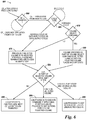
- FIG. 6 is a flow chart illustrating a method 601 for controlling memory in accordance with a number of embodiments of the present disclosure.
- the method 601 can be applied to various memory systems such as those described above in Figures 1-5 .
- the method 601 can apply to a number of memory devices coupled to a system controller via a shared bus.
- the number of memory devices share a chip enable signal (CE_n) from the system controller and arc active low (e.g., the memory units of the devices activate upon detection of a low signal state of the chip enable signal).
- CE_n chip enable signal
- the memory units e.g., LUNs
- volume addresses can be assigned to target memory volumes within the memory devices.
- a target memory volume can include a number of memory units sharing a chip enable signal within a memory device (e.g., a package).
- the volume addresses can be assigned to the target memory volumes upon initialization of the system (e.g., upon power up).
- the assigned volume addresses can be maintained across reset commands, in a number of embodiments, and different volume addresses can be assigned to the target memory volumes upon a subsequent system initialization.
- the memory units sharing a chip enable signal can each enter an inactive (e.g., deselected) state from a previous state due to a transition of the shared chip enable signal from a low to high state.
- an inactive e.g., deselected
- the memory volumes prior to the chip enable signal transition to the high state, one of the memory volumes (and, therefore, a number of memory units) on the shared bus would be active (e.g., due to a low chip enable signal received thereto) and being used by the system controller (e.g., processing commands from the controller).
- the system controller e.g., processing commands from the controller
- the memory volumes wait for a switching of the chip enable signal from the high (e.g., inactive) to low (e.g., active) state.
- the memory volumes sharing the chip enable signal activate and determine a cycle type (e.g., command, address, or data) of the next cycle issued by the system controller.
- a cycle type e.g., command, address, or data
- the previously selected memory volume e.g., the memory volume which was active and being used by the controller prior to the transition of the chip enable signal to the high state
- the cycle is a command cycle (e.g., as opposed to an address cycle and/or a data cycle).
- the previously selected memory volume (e.g., the memory device that includes the previously selected memory volume) is reselected responsive to the cycle type being an address cycle, data input cycle, or data output cycle.
- previously assigned terminators for the reselected target memory volume are placed in a sniff state. That is, since the previously selected memory volume is reselected, those memory units previously assigned as terminators for the selected volume return to their previous state, which is a sniff state. As such, the memory units assigned as terminators for the selected volume monitor commands provided to the selected volume and perform ODT functions in appropriate circumstances.
- the terminators can be a number of memory units (e.g., LUNs) within the reselected target memory volume or within a number of memory units within an unselected target memory volume.
- the cycle type is a command cycle (e.g., the controller performs a command cycle rather than an address or data cycle)
- a determination can be made as to the type of command provided by the system controller.
- the command provided by the controller may indicate a target memory volume within a particular one of the number of memory devices targeted to execute a number of subsequent commands received thereto.
- each of the number of memory devices return to their previous state.
- the subsequent command(s) provided by the controller are to be executed by a particular memory unit associated with the indicated target memory volume within one of the number of memory devices.
- the previously selected memory volume is reselected unless the command issued by the controller and received by the number of memory volumes is a particular type of command.
- the previously selected memory volume e.g., the memory device that includes the previously selected memory volume
- a volume select command refers to a command issued by the controller that indicates a volume address of a particular target memory volume to receive a subsequent command issued by the controller (e.g., a particular target memory volume that includes the memory unit for which the subsequent command is intended).
- the volume select command is a first command provided by the system controller subsequent to activating the number of memory volumes via the switching of the chip enable signal from the high to the low state.
- a particular target memory volume indicated by the command (e.g., the volume select command) is selected by the system controller.
- the memory device having the selected target memory volume therein is activated and the remaining memory devices return to their respective previous states.
- the selected target volume remains active and the number of memory units corresponding the selected target volume execute subsequent commands from the system controller until a subsequent deactivation of the selected target volume (e.g., due to a switching of the chip enable signal to a high state).
- terminators for the selected target volume can be placed in a sniff state while the selected target volume remains selected.
- the method 601 includes determining whether a memory unit is part of the currently selected target memory volume or whether the memory unit is in a sniff state. If the memory unit is not part of the currently selected target memory volume and is not in a sniff state, then as illustrated at block 690, the memory unit deselects and remains inactive until a next transition of the chip enable signal from the high to the low state. If the memory unit is part of the currently selected target memory volume, then as illustrated at block 695, the memory unit proceeds to execute the command, if applicable. Also, if the memory system includes an enabled on die termination function, then appropriate ODT actions for memory units of the selected volume can be performed.
- the memory unit can proceed to perform appropriate ODT actions for memory units on the unselected target memory volume.
- Embodiments of the present disclosure are not limited to the example illustrated in Figure 6 .
- the present disclosure includes systems, devices, memory controllers, and methods for controlling memory.
- One such method includes activating a memory unit of a memory device; after activating the memory unit, providing a command to the memory device; and returning the memory unit to a previous state if the command does not indicate a target memory volume, wherein the memory unit remains active if the command indicates a target memory volume associated with the memory unit.
Landscapes
- Engineering & Computer Science (AREA)
- Theoretical Computer Science (AREA)
- Physics & Mathematics (AREA)
- General Engineering & Computer Science (AREA)
- General Physics & Mathematics (AREA)
- Human Computer Interaction (AREA)
- Techniques For Improving Reliability Of Storages (AREA)
- Memory System (AREA)
- Information Retrieval, Db Structures And Fs Structures Therefor (AREA)
Abstract
Description
- The present disclosure relates generally to semiconductor memory systems, devices, and methods, and more particularly, to systems, devices, memory controllers, and methods for controlling memory.
- Memory devices are typically provided as internal, semiconductor, integrated circuits in computers or other electronic devices. There are many different types of memory including volatile and non-volatile memory. Volatile memory can require power to maintain its information and includes random-access memory (RAM), dynamic random access memory (DRAM), and synchronous dynamic random access memory (SDRAM), among others. Non-volatile memory can provide persistent information by retaining stored information when not powered and can include NAND flash memory, NOR flash memory, read only memory (ROM), Electrically Erasable Programmable ROM (EEPROM), Erasable Programmable ROM (EPROM), phase change random access memory (PCRAM), resistive random access memory (RRAM), and magnetic random access memory (MRAM), such as spin torque transfer random access memory (STT RAM), among others.
- Memory devices can be combined together to form a solid state drive (SSD). A solid state drive can include non-volatile memory (e.g., NAND flash memory and NOR flash memory), and/or can include volatile memory (e.g., DRAM and SRAM), among various other types of non-volatile and volatile memory. An SSD can be used to replace hard disk drives as the main storage device for a computer, as the solid state drive can have advantages over hard drives in terms of performance, size, weight, ruggedness, operating temperature range, and power consumption. For example, SSDs can have superior performance when compared to magnetic disk drives due to their lack of moving parts, which may avoid seek time, latency, and other electromechanical delays associated with magnetic disk drives. SSD manufacturers can use non-volatile flash memory to create flash SSDs that may not use an internal battery supply, thus allowing the drive to be more versatile and compact.
- An SSD can include one or more discrete memory devices (e.g., packages), which can be multi-chip packages (MCPs). A MCP can include a number of memory dies and/or chips each having one or more memory units associated therewith. The memory units can execute commands received from a host, report status to the host, and can include one or more memory arrays along with peripheral circuitry. The memory arrays can include memory cells that can be organized into a number of physical groups (e.g., blocks), with each of the groups capable of storing multiple pages of data.
- In various memory systems, multiple memory devices are coupled to a system controller via a shared bus. The system controller can regulate performance of various operations such as erase operations, program operations, and read operations, for example. The interaction between the system controller and the multiple memory devices can affect various characteristics of a memory system including power consumption, processing speed, and/or data integrity, among other memory system characteristics.
-
-
Figure 1 is a block diagram of a computing system in accordance with one or more embodiments of the present disclosure. -
Figure 2 is a block diagram of a portion of a system configured to control memory in accordance with one or more embodiments of the present disclosure. -
Figure 3 is a block diagram of a portion of a system configured to control memory in accordance with one or more embodiments of the present disclosure. -
Figure 4 is a block diagram of a portion of a system configured to control memory in accordance with one or more embodiments of the present disclosure. -
Figure 5 is a block diagram of a portion of a system configured to control memory in accordance with one or more embodiments of the present disclosure. -
Figure 6 is a flow chart illustrating a method for controlling memory in accordance with one or more embodiments of the present disclosure. - The present disclosure includes systems, devices, memory controllers, and methods for controlling memory. One such method includes activating a memory unit of a memory device; after activating the memory unit, providing a command to the memory device; and returning the memory unit to a previous state if the command docs not indicate a target memory volume, wherein the memory unit remains active if the command indicates a target memory volume associated with the memory unit.
- Embodiments of the present disclosure can provide various benefits such as reducing interaction between a memory system controller and memory devices coupled to the system controller via a shared bus in association with various memory operations as compared to prior memory systems, devices, and methods, among other benefits. As an example, reducing the interaction between the system controller and the memory devices can reduce power consumption associated with operating the memory system.
- In the following detailed description of the present disclosure, reference is made to the accompanying drawings that form a part hereof, and in which is shown by way of illustration how one or more embodiments of the disclosure may be practiced. These embodiments are described in sufficient detail to enable those of ordinary skill in the art to practice the embodiments of this disclosure, and it is to be understood that other embodiments may be utilized and that process, electrical, and/or structural changes may be made without departing from the scope of the present disclosure. As used herein, the designators "N," and "M," particularly with respect to reference numerals in the drawings, indicates that a number of the particular feature so designated can be included with one or more embodiments of the present disclosure. As used herein, "a number of' something can refer to one or more of such things.
- The figures herein follow a numbering convention in which the first digit or digits correspond to the drawing figure number and the remaining digits identify an element or component in the drawing. Similar elements or components between different figures may be identified by the use of similar digits. For example, 104 may reference element "04" in
Figure 1 , and a similar element may be referenced as 204 inFigure 2 . As will be appreciated, elements shown in the various embodiments herein can be added, exchanged, and/or eliminated so as to provide a number of additional embodiments of the present disclosure. In addition, as will be appreciated, the proportion and the relative scale of the elements provided in the figures are intended to illustrate the embodiments of the present invention, and should not be taken in a limiting sense. -
Figure 1 is a functional block diagram of acomputing system 100 in accordance with a number of embodiments of the present disclosure.Computing system 100 includes amemory system 104, for example a number of solid state drives (SSDs), communicatively coupled tohost 102.Memory system 104 can be communicatively coupled to thehost 102 through aninterface 106, such as a backplane or bus, for instance. - Examples of
hosts 102 can include laptop computers, personal computers, digital cameras, digital recording and playback devices, mobile telephones, PDAs, memory card readers, and interface hubs, among other host systems. Theinterface 106 can include a serial advanced technology attachment (SATA), peripheral component interconnect express (PCIe), or a universal serial bus (USB), among other connectors and interfaces. In general, however,host interface 106 can provide an interface for passing control, address, data, and other signals between thememory system 104 and thehost 102. -
Host 102 can include a number of processors 105 (e.g., parallel processors, co-processors, etc.) communicatively coupled to a memory andbus control 107. Theprocessor 105 can be a number of microprocessors, or some other type of controlling circuitry, such as a number of application-specific integrated circuits (ASICs), for example. Other components of thecomputing system 100 may also have processors. The memory andbus control 107 can have memory and other components directly communicatively coupled thereto, for example, dynamic random access memory (DRAM) 111,graphic user interface 118, and/or other user interface (e.g., display monitor, keyboard, mouse, etc.). - The memory and
bus control 107 can also have a peripheral andbus control 109 communicatively coupled thereto, which in turn, can connect to a number of devices, such as aflash drive 119 using a universal serial bus (USB) interface, for example, a non-volatile memory host control interface (NVMHCT)flash memory 117, and/or thememory system 104. As the reader will appreciate, thememory system 104 can be used in addition to, or in lieu of, a hard disk drive (HDD) in a number of different computing systems. Thecomputing system 100 illustrated inFigure 1 is one example of such a system; however, embodiments of the present disclosure are not limited to the configuration shown inFigure 1 . - Enterprise solid state storage appliances arc a class of memory systems that can currently be characterized by terabytes of storage and fast performance capabilities, for example 100MB/sec, 100K inputs/outputs per second (IOPS), etc. According to a number of embodiments of the present disclosure, an enterprise solid state storage appliance can be configured using solid state drive (SSD) components. For example, with respect to
Figure 1 , thememory system 104 may be an enterprise solid state storage appliance implemented using a number of component SSDs, the number of SSDs being operated as a memory system by a memory system controller (e.g.,memory system controller 215 shown inFigure 2 ). -
Figure 2 is a block diagram of a portion of asystem 200 configured to control memory in accordance with a number of embodiments of the present disclosure. Thesystem 200 includes amemory system 204, which can be a SSD, for example. Thememory system 204 can be coupled to ahost 202 via ahost interface 206 and can include a memory system controller 215 (e.g., memory control circuitry, firmware, and/or software), and a number of memory devices 230-1, ..., 230-N coupled to thesystem controller 215. In a number of embodiments, thememory controller 215 can be an application specific integrated circuit (ASIC) coupled to a printed circuit board. - The
memory system 204 includes abus 220 to send/receive various signals (e.g., data signals, control signals, and/or address signals), between the memory devices 230-1, ..., 230-N and thesystem controller 215. Although the example illustrated inFigure 2 includes asingle bus 220, thememory system 204 can include a separate data bus (DQ bus), control bus, and address bus, in some embodiments. Thebus 220 is shared by the number of memory devices 230-1, ..., 230-N and can have various types of bus structures including, but not limited to, bus structures related to Open NAND Flash Interface (ONFT), Compact Flash Interface, Multimedia Card (MMC), Secure Digital (SD), CE-ATA, Industrial Standard Architecture (ISA), Micro-Channel Architecture (MSA), Extended ISA (EISA), Intelligent Drive Electronics (IDE), VESA Local Bus (VLB), Peripheral Component Interconnect (PCI), Card Bus, Universal Serial Bus (USB), Advanced Graphics Port (AGP), Personal Computer Memory Card International Association bus (PCMCIA), Firewire (IEEE 1394), and Small Computer Systems Interface (SCSI). - As illustrated in
Figure 2 , the memory devices 230-1, ..., 230-N can comprise a number of dies and/or chips that can include a number of memory units 212-1, 212-2, ..., 212-M providing a storage volume for thememory system 204. The memory units 212-1, 212-2, ..., 212-M can be referred to as logical units (LUNs) and can include a number of memory arrays along with peripheral circuitry thereon. In a number of embodiments, the memory units 212-1, 212-2, ..., 212-M can be the minimum component ofmemory system 204 capable of independently executing commands from and reporting status to thememory system controller 215 and/or host 202 viabus 220. The memory units 212-1, 212-2, ..., 212-M can include Flash memory arrays having a NAND architecture, for example. However, embodiments are not limited to a particular type of memory array or array architecture. - As described further below in connection with
Figures 3-6 , the memory units 212-1, 212-2, ..., 212-M within the memory devices 230-1, ..., 230-N can be organized into a number of target volumes. In a number of embodiments, each target volume can be a set of memory units that share an enable signal (e.g., a chip enable (CE) signal received from controller 215) within one of the memory devices 230-1, ..., 230-N. For instance, a number of enable terminals (e.g., pins) associated with the memory devices 230-1, ..., 230-N can be coupled together and may be coupled to one enable terminal (e.g., pin) of thecontroller 215. As such, a single chip enable pin of the controller may be shared by a number of the memory devices 230-1, ..., 230-N, in various embodiments. - As one of ordinary skill in the art will appreciate, the state of a chip enable signal can be used to activate/deactivate a memory unit. For example, a memory system can be configured such that memory units arc active low (e.g., the memory units can process commands received from the system controller when the chip enable signal is in a low state). For active low memory units, the memory units become inactive (e.g., deselected) and cannot process commands when the chip enable signal is in a high state. Embodiments of the present disclosure are not limited to memory units having a particular chip enable configuration. As used herein, activating a memory unit can include activating a target memory volume and/or a memory device associated with a memory unit.
- The target volumc(s) within the memory devices 230-1, ..., 230-N can have volume addresses assigned (e.g., appointed) thereto. The assigned volume addresses can be used to distinguish among target volumes associated with a shared chip enable signal, as described further below.
-
Figure 3 is a block diagram of a portion of a system configured to control memory in accordance with a number of embodiments of the present disclosure. The memory system illustrated inFigure 3 includes asystem controller 325. Thesystem controller 325 can control access across a number of memory channels. In this example, thecontroller 325 includes a number of channel controllers 327-0, ..., 327-N each controlling access to a respective memory channel. - In the example shown in
Figure 3 , thesystem controller 325 is coupled to a first memory device 330-1 and a second memory device 330-2 via a bus 320 (e.g., a shared data, address, and control bus). Each of the memory devices 330-1 and 330-2 includes 4 memory units 312-0 to 312-3. The memory units 312-0 to 312-3 can be memory die and the memory devices 330-1 and 330-2 can be multi-chip packages, as an example. In this example, the memory units 312-0 to 312-3 within each memory device are organized (e.g., grouped) into two target volumes, with each of the memory units of a target volume sharing a chip enable pin. For instance, memory units 312-0 and 312-1 comprise target volume 313-0 and memory units 312-2 and 312-3 comprise target volume 313-1 within memory device 330-1. Similarly, memory units 312-0 and 312-1 comprise target volume 313-2 and memory units 312-2 and 312-3 comprise target volume 313-3 within memory device 330-2. - In this example, the system controller includes four CE pins 328-0 (CE0), 328-1 (CE1), 328-2 (CE2), and 328-3 (CE3) dedicated to providing CE signals to the memory devices 330-1 and 330-2. For instance, CE0 is coupled to a CE pin associated with target volume 313-0 within memory device 330-1, CE1 is coupled to a CE pin associated with target volume 313-1 within memory device 330-1, CE2 is coupled to a CE pin associated with target volume 313-2 within memory device 330-2, and CE3 is coupled to a CE pin associated with target volume 313-3 within memory device 330-2.
- One of ordinary skill in the art will appreciate that although the CE pins are shown separately, the
controller 325 and memory devices 330-1 and 330-2 have various other pins connected via signal lines, for instance, which can be part ofbus 320. Although not shown inFigure 3 , each of the channel controllers 327-0 to 327-N can be coupled to a number of memory devices (e.g., two in this example). Embodiments are not limited to the example shown inFigure 3 . For instance, the memory system can include more or fewer than two memory devices per channel, more or fewer than two target memory volumes per memory device, etc. - In the example illustrated in
Figure 3 , each of the target memory volumes 313-0 to 313-3 has an assigned volume address associated therewith. As described further below in connection withFigure 6 , a command provided (e.g., issued) by thecontroller 325 can indicate (e.g., specify) a volume address of a particular one of the target memory volumes to receive a number of subsequent commands (e.g., the next command) from the controller. The command indicating the particular target volume address is received by each of the memory devices coupled to the sharedbus 320. In various embodiments, those memory units and/or associated target volumes not specified by the command revert to an unselected state. As used herein, an unselected state can be, for example, an inactive state or a "snooping" (e.g., sniff) state, as described further below. In a number of embodiments, those memory units and/or associated target volumes not specified by the command revert to their previous states. For instance, a memory unit of the target memory volume specified by the command remains active and the memory units associated with the remaining target memory volumes return to their previous unselected states. For instance, when thecontroller 325 wants to maintain interaction with a target volume (e.g., with a particular memory unit associated with a target volume) within a particular one of the memory devices 330-1 and 330-2 coupled to the sharedbus 320, those memory devices including unselected volumes can revert to an unselected state. Depending on which target volume is selected and/or how the system is configured, the memory units of the unselected memory devices may return to their previous states, switch from an inactive state to a snooping state, switch from a sniff state to an inactive state, or switch from the active state to the inactive state or sniff state. -
Figure 4 is a block diagram of a portion of a system configured to control memory in accordance with a number of embodiments of the present disclosure. The embodiment illustrated inFigure 4 can provide reduced pin counts as compared with the memory system illustrated inFigure 3 . The memory system illustrated inFigure 4 includes asystem controller 425. Thesystem controller 425 can control access across a number of memory channels. In this example, thecontroller 425 includes a number of channel controllers 427-0, 427-1, ..., 427-N each controlling access to a respective memory channel. - In the example shown in
Figure 4 , thechannel controller 425 is coupled to a number of memory devices 430-1, ..., 430-M via a bus 420 (e.g., a data, address, and control bus). In this embodiment, each of the memory devices 430-1, ..., 430-M includes 4 memory units 412-0 to 412-3. Similar to the system described inFigure 3 , in this example, the memory units 412-0 to 412-3 within each memory device are organized into two target volumes, with each of the memory units of a target volume sharing a chip enable pin. For instance, memory units 412-0 and 412-1 comprise target volume 413-0 and memory units 412-2 and 412-3 comprise target volume 413-1 within memory device 430-1. Similarly, memory units 412-0 and 412-1 comprise target volume 413-2 and memory units 412-2 and 412-3 comprise target volume 413-3 within memory device 430-M. - In this example, the
system controller 425 includes two CE pins 428-0 (CE0) and 428-1 (CE1) dedicated to providing CE signals to the memory devices 430-1 to 430-M. For instance, CE0 is coupled to a CE pin associated with target volume 413-0 within memory device 430-1 and a CE pin associated with target volume 413-2 within memory device 430-M. Also, CE1 is coupled to a CE pin associated with target volume 413-1 within memory device 430-1 and a CE pin associated with target volume 413-3 within memory device 430-M. As such, a single chip enable signal provided via a single chip enable pin of thecontroller 425 can be shared by multiple target memory volumes across a number of memory devices coupled to acommon bus 420. -
Figure 5 is a block diagram of a portion of a system configured to control memory in accordance with a number of embodiments of the present disclosure. The embodiment illustrated inFigure 5 includes a number of memory devices 530-0, 530-1, 530-2, and 530-3 and illustrates an example topology for controlling memory in accordance with a number of embodiments of the present disclosure. The memory devices 530-0, 530-1, 530-2, and 530-3 can each be single memory volume devices; however, embodiments arc not so limited. As an example, the memory devices 530-0, 530-1, 530-2, and 530-3 can be NAND memory devices. - In the example illustrated in
Figure 5 , each of the devices 530-0, 530-1, 530-2, and 530-3 includes an input pin 539 and an output pin 541. For instance, device 530-0 includes input pin 539-0 (ENi_0) and output pin 541-0 (ENo_0), device 530-1 includes input pin 539-1 (ENi_1) and output pin 541-1 (ENo_1), device 530-2 includes input pin 539-2 (ENi_2) and output pin 541-2 (ENo_2), and device 530-3 includes input pin 539-3 (ENi_3) and output pin 541-3 (ENo_3). - As illustrated, the input pins 539 and output pins 541 of the memory devices 530-0, 530-1, 530-2, and 530-3 can be coupled to create a daisy chain configuration. In this example, the input pin 539-0 of the first device 530-0 in the chain and the output pin 541-3 of the last device 530-3 in the chain are not connected (NC). The input pins 539 of the other devices are connected to the output pin 541 of the previous device in a daisy chain configuration as shown in
Figure 5 . Embodiments of the present disclosure are not limited to the topology illustrated inFigure 5 . For instance, embodiments are not limited to a daisy chain topology. - As illustrated in
Figure 5 , and as described above in connection withFigure 4 , each of the memory devices 530-0, 530-1, 530-2, and 530-3 share a common CE pin from a system controller (e.g.,system controller 425 shown inFigure 4 ). For instance, a chip enable signal 544 (CE0_N) from a system controller is shared by the chip enable pin 538-1 (CE1) of each of the memory devices 530-0, 530-1, 530-2, and 530-3. The CE1 pin of each of the memory devices 530-0, 530-1, 530-2, and 530-3 is associated with (e.g., corresponds to) a particular target memory volume 513-0, 513-1, 513-2, 513-3. As described above, a target volume can refer to a number of memory units (e.g., LUNs) that share a particular CE signal within a memory device. Each of the target volumes can be assigned a volume address. In this example, target volume 513-0 is assigned volume address H0N0, target volume 513-1 is assigned volume address H0N1, target volume 513-2 is assigned volume address H0N2, and target volume 513-3 is assigned volume address H0N3. In a number of embodiments, the volume addresses can be assigned to particular target volumes upon initialization of the memory system. - In operation, the states of the input pins 539-0, 539-1, 539-2, and 539-3 and of the chip enable pin 538-1 (e.g., based on the state of chip enable signal 544) determines whether the respective memory device 530-0, 530-1, 530-2, and 530-3 is able to accept commands. For example, if the input pin 539 of a particular device is high and the CE pin 538-1 of the device is low, then the particular device can accept commands. If the enable input of the particular device is low or the CE pin 538-1 is high, then the device cannot accept commands.
- In a number of embodiments, a system controller can issue a command indicating a target volume address of a particular target volume to process a number of subsequent commands. For instance, a volume select command can be issued by the system controller to the number of memory devices 530-0, 530-1, 530-2, and 530-3 (e.g., via a shared bus) in order to select a particular target volume (e.g., 513-0, 513-1, 513-2, 513-3) sharing a particular chip enable
signal 544 from the system controller. In this manner, volume addressing can be used to access particular target volumes of the memory devices 530-0, 530-1, 530-2, and 530-3. - In a number of embodiments, a chip enable signal (e.g., chip enable signal 544) received from a system controller (via a shared bus such as shared
bus 420 shown inFigure 4 ) is used to activate a number of memory units in memory devices (e.g., 530-0, 530-1, 530-2, and 530-3). For example, assuming the memory units in memory devices 530-0, 530-1, 530-2, and 530-3 are active low, they can be activated responsive to detecting the chip enablesignal 544 switching from a first state to a second state (e.g., from a high to a low state). - A command can subsequently be provided to the activated number of memory units in memory devices 530-0, 530-1, 530-2, and 530-3. In a number of embodiments, the command can indicate (e.g., via a target memory volume address) a target memory volume of the number of target memory volumes (e.g., 513-0, 513-1, 513-2, 513-3) within a particular one of the number of memory devices 530-0, 530-1, 530-2, and 530-3. The target memory volume indicated by the command remains active (e.g., selected) and, if that volume was active in its previous state, the remaining memory volumes return to their previous states (e.g., their respective unselected states prior to activation responsive to detecting the switching of the chip enable signal).
- If the command received subsequent to activation responsive to switching of the chip enable signal does not indicate a target volume (e.g., the command is not a volume select command), then each of the memory devices 530-0, 530-1, 530-2, and 530-3 and target memory volumes therein return to their previous states. As such, a previously selected one of the number of memory volumes (e.g., the memory volume which was selected prior to detecting the switching of the enable signal) will remain selected. Also, those memory volumes which were previously unselected will return to an unselected state. As described further below, an unselected state may include, for example, an inactive state or a "snooping" (e.g., sniff) state (e.g., if an on die termination function is enabled), in a number of embodiments. On die termination (ODT) refers to the use of a number of memory units (e.g., die) to perform termination for a number of signal lines of a shared bus. ODT can improve signal integrity associated with signals across shared busses. As an example, a number of memory units can be assigned as terminators for particular memory volumes such that the number of memory units perform termination functions when the particular memory volume is selected. As an example, when a particular volume is selected, the memory units assigned as terminators for that particular volume can enter a sniff state in which they monitor commands provided to the selected volume. The memory units assigned as terminators can activate upon detection of a particular operation (e.g., a read command, a write command, etc.) in order to perform a termination function. The memory unit can then return to a sniff state such that it does not remain active. Maintaining memory volumes in a sniff state can reduce system power usage as compared to maintaining the memory volumes in an active state, among other benefits.
-
Figure 6 is a flow chart illustrating amethod 601 for controlling memory in accordance with a number of embodiments of the present disclosure. Themethod 601 can be applied to various memory systems such as those described above inFigures 1-5 . As an example, themethod 601 can apply to a number of memory devices coupled to a system controller via a shared bus. In this example, the number of memory devices share a chip enable signal (CE_n) from the system controller and arc active low (e.g., the memory units of the devices activate upon detection of a low signal state of the chip enable signal). The memory units (e.g., LUNs) are each capable of independently executing commands and reporting status to the system controller. In a number of embodiments, volume addresses can be assigned to target memory volumes within the memory devices. A target memory volume can include a number of memory units sharing a chip enable signal within a memory device (e.g., a package). In a number of embodiments, the volume addresses can be assigned to the target memory volumes upon initialization of the system (e.g., upon power up). The assigned volume addresses can be maintained across reset commands, in a number of embodiments, and different volume addresses can be assigned to the target memory volumes upon a subsequent system initialization. - For the
method 601, the memory units sharing a chip enable signal can each enter an inactive (e.g., deselected) state from a previous state due to a transition of the shared chip enable signal from a low to high state. As an example, prior to the chip enable signal transition to the high state, one of the memory volumes (and, therefore, a number of memory units) on the shared bus would be active (e.g., due to a low chip enable signal received thereto) and being used by the system controller (e.g., processing commands from the controller). Upon transition of the chip enable signal from the low to high state, the previously active memory volume and each other memory volume sharing the chip enable signal would be deactivated. As illustrated atblock 660, the memory volumes wait for a switching of the chip enable signal from the high (e.g., inactive) to low (e.g., active) state. - As illustrated at
block 665, upon detection of a switching (e.g., transition) of the chip enable signal from the high to the low state, the memory volumes sharing the chip enable signal activate and determine a cycle type (e.g., command, address, or data) of the next cycle issued by the system controller. In a number of embodiments, the previously selected memory volume (e.g., the memory volume which was active and being used by the controller prior to the transition of the chip enable signal to the high state) is reselected (and the remaining memory volumes are deselected) unless the cycle is a command cycle (e.g., as opposed to an address cycle and/or a data cycle). For instance, as illustrated atblock 675, the previously selected memory volume (e.g., the memory device that includes the previously selected memory volume) is reselected responsive to the cycle type being an address cycle, data input cycle, or data output cycle. Also, as illustrated atblock 675, previously assigned terminators for the reselected target memory volume are placed in a sniff state. That is, since the previously selected memory volume is reselected, those memory units previously assigned as terminators for the selected volume return to their previous state, which is a sniff state. As such, the memory units assigned as terminators for the selected volume monitor commands provided to the selected volume and perform ODT functions in appropriate circumstances. The terminators can be a number of memory units (e.g., LUNs) within the reselected target memory volume or within a number of memory units within an unselected target memory volume. - In the example illustrated in
Figure 6 , if the cycle type is a command cycle (e.g., the controller performs a command cycle rather than an address or data cycle), then atblock 670, a determination can be made as to the type of command provided by the system controller. In a number of embodiments, the command provided by the controller may indicate a target memory volume within a particular one of the number of memory devices targeted to execute a number of subsequent commands received thereto. In a number of embodiments, responsive to the command not indicating a target memory volume within a particular one of the number of memory devices, each of the number of memory devices return to their previous state. In various embodiments, the subsequent command(s) provided by the controller are to be executed by a particular memory unit associated with the indicated target memory volume within one of the number of memory devices. - In a number of embodiments, the previously selected memory volume is reselected unless the command issued by the controller and received by the number of memory volumes is a particular type of command. For instance, as illustrated at
block 675, the previously selected memory volume (e.g., the memory device that includes the previously selected memory volume) is reselected responsive to the command being a command other than a volume select command (e.g., a command such as a read command, write command, erase command, or other command). As used herein, a volume select command refers to a command issued by the controller that indicates a volume address of a particular target memory volume to receive a subsequent command issued by the controller (e.g., a particular target memory volume that includes the memory unit for which the subsequent command is intended). In some embodiments, the volume select command is a first command provided by the system controller subsequent to activating the number of memory volumes via the switching of the chip enable signal from the high to the low state. - As illustrated at
block 680, a particular target memory volume indicated by the command (e.g., the volume select command) is selected by the system controller. As such, the memory device having the selected target memory volume therein is activated and the remaining memory devices return to their respective previous states. As such, the selected target volume remains active and the number of memory units corresponding the selected target volume execute subsequent commands from the system controller until a subsequent deactivation of the selected target volume (e.g., due to a switching of the chip enable signal to a high state). Also, in a number of embodiments, terminators for the selected target volume can be placed in a sniff state while the selected target volume remains selected. - At
block 685, themethod 601 includes determining whether a memory unit is part of the currently selected target memory volume or whether the memory unit is in a sniff state. If the memory unit is not part of the currently selected target memory volume and is not in a sniff state, then as illustrated atblock 690, the memory unit deselects and remains inactive until a next transition of the chip enable signal from the high to the low state. If the memory unit is part of the currently selected target memory volume, then as illustrated atblock 695, the memory unit proceeds to execute the command, if applicable. Also, if the memory system includes an enabled on die termination function, then appropriate ODT actions for memory units of the selected volume can be performed. If it is determined that the memory unit is in a sniff state and is of an unselected target memory volume, then as illustrated atblock 699, the memory unit can proceed to perform appropriate ODT actions for memory units on the unselected target memory volume. Embodiments of the present disclosure are not limited to the example illustrated inFigure 6 . - The present disclosure includes systems, devices, memory controllers, and methods for controlling memory. One such method includes activating a memory unit of a memory device; after activating the memory unit, providing a command to the memory device; and returning the memory unit to a previous state if the command does not indicate a target memory volume, wherein the memory unit remains active if the command indicates a target memory volume associated with the memory unit.
- It will be understood that when an clement is referred to as being "on," "connected to" or "coupled with" another element, it can be directly on, connected, or coupled with the other element or intervening elements may be present. In contrast, when an element is referred to as being "directly on," "directly connected to" or "directly coupled with" another element, there are no intervening elements or layers present. As used herein, the term "and/or" includes any and all combinations of one or more of the associated listed items. As used herein the term "or," unless otherwise noted, means logically inclusive or. That is, "A or B" can include (only A), (only B), or (both A and B). In other words, "A or B" can mean "A and/or B" or "one or more of A and B."
- Although specific embodiments have been illustrated and described herein, those of ordinary skill in the art will appreciate that an arrangement calculated to achieve the same results can be substituted for the specific embodiments shown. This disclosure is intended to cover adaptations or variations of one or more embodiments of the present disclosure. It is to be understood that the above description has been made in an illustrative fashion, and not a restrictive one. Combination of the above embodiments, and other embodiments not specifically described herein will be apparent to those of skill in the art upon reviewing the above description. The scope of the one or more embodiments of the present disclosure includes other applications in which the above structures and methods are used. Therefore, the scope of one or more embodiments of the present disclosure should be determined with reference to the appended claims, along with the full range of equivalents to which such claims are entitled.
- In the foregoing Detailed Description, some features are grouped together in a single embodiment for the purpose of streamlining the disclosure. This method of disclosure is not to be interpreted as reflecting an intention that the disclosed embodiments of the present disclosure have to use more features than are expressly recited in each claim. Rather, as the following claims reflect, inventive subject matter lies in less than all features of a single disclosed embodiment. Thus, the following claims are hereby incorporated into the Detailed Description, with each claim standing on its own as a separate embodiment.
- The disclosure herein also includes the content of the following clauses:
- 1. A method for controlling memory, comprising:
- activating a memory unit of a memory device;
- after activating the memory unit, providing a command to the memory device; and
- returning the memory unit to a previous state if the command does not indicate a target memory volume, wherein the memory unit remains active if the command indicates a target memory volume associated with the memory unit.
- 2. The method of
clause 1, wherein activating the memory unit includes providing an enable signal to the memory device, wherein the memory device shares that enable signal with other memory devices. - 3. The method of
clause 2, wherein activating the memory unit includes switching the shared enable signal from a first state to a second state. - 4. The method of
clause 2, wherein providing the enable signal includes providing the shared enable signal from an enable terminal of a controller to a respective enable terminal associated with the memory device. - 5. The method of any one of
clauses 1 to 4, wherein returning the memory unit to a previous state if the command does not indicate a target memory volume includes returning the memory unit to a previous state if the command does not indicate a volume address. - 6. The method of any one of
clauses 1 to 4, further including deactivating the memory unit prior to activating the memory unit, wherein returning the memory unit to a previous state includes returning the memory unit to a state of the memory unit immediately prior to deactivating the memory unit. - 7. The method of any one of
clauses 1 to 4, wherein the previous state comprises an inactive state. - 8. The method of any one of
clauses 1 to 4, wherein the previous state comprises a snooping state. - 9. The method of any one of
clauses 1 to 4, further including placing a memory unit associated with a memory volume other than the target memory volume in a snooping state responsive to the command indicating the target memory volume. - 10. A method for controlling memory, comprising:
- activating a number of memory volumes by switching an enable signal provided to a number of memory devices from a first state to a second state;
- providing a command to the activated number of memory devices;
- responsive to the command being a command other than a volume select command, a memory volume of the number of memory volumes that was previously active prior to switching the signal remains active; and
- responsive to the command being a volume select command, the memory volume indicated by the volume select command remains active.
- 11. The method of clause 10, including, responsive to the command being a volume select command, returning at least one of the memory volumes not indicated by the volume select command to its state prior to the switching of the signal.
- 12. The method of any one of clauses 10 to 11, including, responsive to the command being a command other than a volume select command, memory volumes of the number of memory volumes not previously active prior to switching the signal return to their respective states prior to the switching of the signal.
- 13. A method for operating a number of memory devices each including one or more target memory volumes therein, the method comprising:
- activating a number of memory volumes of the number of memory devices responsive to detecting a switching of a signal from a first state to a second state;
- subsequently receiving a command with the number of memory devices;
- wherein, responsive to the command indicating a target memory volume within a particular one of the number of memory devices, the particular one of the number of memory devices executes a subsequent command received thereto; and
- wherein, responsive to the command not indicating a target memory volume within a particular one of the number of memory devices, each of the number of memory devices returns to a previous device state.
- 14. The method of clause 13, wherein subsequently receiving a command includes receiving the command via a bus shared by the number of memory devices.
- 15. The method of clause 14, including at least two of the number of memory devices receiving the signal from a single chip enable terminal of a controller coupled to the number of memory devices via the shared bus.
- 16. The method of any one of clauses 13 to 15, wherein, responsive to the command indicating a target memory volume within a particular one of the number of memory devices, at least one of the memory devices other than the particular one of the number of memory devices returns to its respective state prior to the detected switching.
- 17. A method for controlling memory, comprising:
- activating a number of memory volumes each having a previous state associated therewith; and
- subsequently providing a select command to the activated number of memory volumes, the select command indicating an address of a selected one of the number of memory volumes to receive a subsequent command for execution;
- wherein at least one of the memory volumes indicated by the select command returns to its respective previous state.
- 18. The method of clause 17, wherein activating a number of memory volumes includes activating the number of memory volumes via toggling an enable signal shared by the number of memory volumes from a first state to a second state.
- 19. The method of clause 18, including providing the enable signal to the number of memory volumes from a controller, wherein an enable terminal of the controller is coupled to a respective enable terminal of each of a number of memory devices.
- 20. The method of clause 19, wherein a number of memory units associated with the activated volumes share the enable signal within the number of memory devices.
- 21. The method of clause 19, wherein the enable terminal of the controller is a chip enable pin and the enable terminal of each of the number of memory devices is a chip enable pin, and wherein providing the enable signal includes providing a chip enable signal to the number of memory devices.
- 22. The method of any one of clauses 17 to 21, including providing the subsequent command for execution to the selected one of the number of memory volumes.
- 23. A memory controller, comprising:
- a first interface for coupling to a host; and
- a second interface for coupling to a number of memory devices, and wherein the memory controller is configured to:
- activate a number of memory volumes of the number of memory devices by switching a shared signal provided thereto from a first state to a second state; and
- subsequently provide a command to the number of memory devices;
- wherein, responsive to the command indicating one of the memory volumes, the one of the memory volumes remains active and executes a subsequent command received from the memory controller; and
- wherein, responsive to the command not indicating any of the number of memory volumes, each of the number of memory volumes returns to its respective state prior to detecting the switching.
- wherein a state of one of the memory devices prior to detecting the switching is an active state and a state of the remaining memory devices prior to detecting the switching is an inactive state
- until the memory system controller subsequently switches the shared enable signal to the first state
- 24. The memory system controller of clause 23, wherein responsive to the command indicating a target memory volume other than a memory volume that was in an active state prior to the switching, at least one of the memory volumes other than the target memory volume returns to its state prior to detecting the switching.
- 25. The memory system controller of any one of clauses 23 to 24, wherein the shared signal is provided from a single chip enable terminal of the memory controller to a respective chip enable terminal of each of the number of memory devices.
- 26. A method for controlling memory, comprising:
- activating a number of memory volumes sharing a bus by switching a signal provided to the number of memory volumes from a first state to a second state;
- responsive to a first command provided to the activated number of memory volumes subsequent to the switching of the signal being a command other than a volume select command, reselecting a volume of the number of volumes that was selected prior to the switching the signal; and
- responsive to the first command provided to the activated number of memory volumes subsequent to the switching of the signal being a volume select command, selecting a volume of the number of volumes indicated by the volume select command.
- 27. A memory system comprising a memory unit configured to:
- activate responsive to detection of a switching of a signal from a first state to a second state;
- receive a command and execute a subsequent command responsive to the command indicating an address of a volume associated with the memory unit; and
- return to a previous state responsive to the command not indicating an address of a target volume, the previous state being a state of the memory unit prior to detection of the switching of the signal.
- 28. The memory system of clause 27, wherein the memory unit comprises a memory device having an enable terminal associated with the memory unit, and further including a controller having an enable terminal, wherein the enable terminal of the memory device is configured to receive the signal from the enable terminal of the controller.
- 29. The memory system of clause 27, wherein the memory system is configured to assign the address of the volume upon initialization of the system.
- 30. The memory system of any one of clauses 27 to 29, wherein the memory system is configured to maintain the address of the volume across reset commands.
- 31. A memory system comprising a memory volume configured to:
- activate responsive to detection of a switching of a signal from a first state to a second state;
- receive a command and execute a subsequent command responsive to the command indicating the volume; and
- return to a previous state responsive to the command not indicating the volume.
- 32. The memory system of clause 31, wherein the volume has an address associated therewith.
- 33. The memory system of clause 32, wherein the command indicates the volume by providing the addresses.
- 34. The memory system of clause 32, wherein the system is configured to assign the address upon initialization of the memory system.
- 35. The memory system of any one of clauses 31 to 34, wherein the volume includes a number of memory units each including a memory array and each capable of independently executing commands and reporting status.
- 36. The memory system of any one of clauses 31 to 34, wherein the command is a first command received by the volume subsequent to activating responsive to detection of the switching of the signal.
- 37. The memory system of any one of clauses 31 to 34, wherein the signal is shared by another volume.
- 38. The memory system of clause 37, wherein each of the volumes is associated with a respective enable terminal of a respective memory device.
- 39. The memory system of clause 38, wherein the signal is a chip enable signal and wherein each of the enable terminals is a respective chip enable pin of the respective memory device.
- 40. A method for controlling memory, comprising:
- activating a number of memory devices each including a number of memory volumes;
- providing a command to the activated number of memory devices; and
- responsive to the command indicating a memory volume of the number of memory volumes within one of the number of memory devices, the memory volume indicated by the command remains active and the remaining target memory volumes are placed in an unselected state.
Claims (15)
- An apparatus, comprising:a memory controller (215; 325; 425); anda plurality of memory devices (230-1, ..., 230-N; 330-1, 330-2; 430-1, ..., 430-M; 530-0, 530-1, 530-2, 530-3) configured to receive a shared chip enable signal from the memory controller,wherein the memory controller (215; 325; 425) is configured to:transition a state of the shared chip enable signal to activate a memory volume (313-0, 313-1, 313-2, 313-3; 413-0, 413-1, 413-2,413-3; 513-0, 513-1, 513-2, 513-3) of each of the plurality of memory devices; andissue a cycle to the plurality of memory devices (230-1, ..., 230-N; 330-1, 330-2; 430-1, ..., 430-M; 530-0, 530-1, 530-2, 530-3),wherein each of the plurality of memory devices is configured to:
responsive to the cycle being a command cycle:maintain the corresponding memory volume (313-0, 313-1, 313-2, 313-3; 413-0, 413-1, 413-2,413-3; 513-0, 513-1, 513-2, 513-3) in an active state and execute a subsequent command from the memory controller (215; 325; 425) if the command corresponding to the command cycle is a volume select command that targets the corresponding memory volume; andreturn the corresponding memory volume (313-0, 313-1, 313-2, 313-3; 413-0, 413-1, 413-2,413-3; 513-0, 513-1, 513-2, 513-3) to its state prior to being activated if the command corresponding to the command cycle is not a volume select command. - The apparatus of claim 1, wherein the memory controller is configured to, prior to activating the memory volume of each of the plurality of memory devices, transition the state of the shared chip enable signal to deactivate the memory volume of each of the plurality of memory devices.
- The apparatus of claim 2, wherein each of the plurality of memory devices is further configured to, responsive to the cycle not being a command cycle, return the corresponding memory volume to an activated state if the memory volume was in an activated state prior to deactivation via the shared chip enable signal.
- The apparatus of claim 2, wherein each of the plurality of memory devices is further configured to, responsive to the cycle not being a command cycle, return the corresponding memory volume to an unselected state if the memory volume was in an unselected state prior to deactivation via the shared chip enable signal.
- The apparatus of claim 4, wherein the unselected state is one of an inactive state and a snoop state.
- The apparatus of claim 1, wherein the cycle is one of a data cycle or an address cycle.
- The apparatus of claim 1, wherein the memory volume of each of the plurality of memory devices comprises a number of logical units (LUNs) (212-1, 212-2, ..., 212-M; 312-0, 312-1, 312-2, 312-3; 412-0, 412-1, 412-2, 412-3).
- The apparatus of claim 1, wherein the memory controller is coupled to the plurality of memory devices (230-1, ..., 230-N; 330-1, 330-2; 430-1, ..., 430-M; 530-0, 530-1, 530-2, 530-3) via a device interface (220; 320; 420) and is coupleable to a host via a host interface (106; 206).
- The apparatus of claim 8, wherein the device interface comprises a shared Open NAND Flash Interface, ONFI, bus.
- The apparatus of claim 1, wherein the memory controller comprises a plurality of channel controllers corresponding to respective memory channels.
- A method, comprising:activating a memory volume (313-0, 313-1, 313-2, 313-3, 413-0, 413-1, 413-2, 413-3, 513-0, 513-1, 513-2, 513-3) of each of a plurality of memory devices (230-1, ..., 230-N; 330-1, 330-2; 430-1, ..., 430-M; 530-0, 530-1, 530-2, 530-3) configured to receive a shared chip enable signal;determining a cycle type of a cycle subsequently issued by a controller (215; 325; 425) coupled to the plurality of memory devices (230-1, ..., 230-N; 330-1, 330-2; 430-1, ..., 430-M; 530-0, 530-1, 530-2, 530-3);for each activated memory volume, responsive to the cycle being a command cycle:maintaining the memory volume (313-0, 313-1, 313-2, 313-3; 413-0, 413-1, 413-2,413-3; 513-0, 513-1, 513-2, 513-3) in an active state and executing a subsequent command from the memory controller (215; 325; 425) if the command corresponding to the command cycle is a volume select command that targets the memory volume; andreturning the memory volume (313-0, 313-1, 313-2, 313-3; 413-0, 413-1, 413-2,413-3; 513-0, 513-1, 513-2, 513-3) to its state prior to being activated if the command corresponding to the command cycle is not a volume select command.
- The method of claim 11, further comprising, prior to activating the memory volume of each of the plurality of memory devices, transitioning the state of the shared chip enable signal to deactivate the memory volume of each of the plurality of memory devices.
- The method of claim 12, further comprising, responsive to the cycle not being a command cycle, returning the memory volume to an activated state if the memory volume was in an activated state prior to deactivation via the shared chip enable signal.
- The method of claim 12, further comprising, responsive to the cycle not being a command cycle, returning the corresponding memory volume to an unselected state if the memory volume was in an unselected state prior to deactivation via the shared chip enable signal.
- The method of claim 11, further comprising, responsive to the command being a volume select command, placing a memory unit associated with a memory volume other than the memory volume targeted by the volume command in a snooping state.
Priority Applications (1)
| Application Number | Priority Date | Filing Date | Title |
|---|---|---|---|
| EP24162066.5A EP4357926B1 (en) | 2011-03-11 | 2012-03-07 | Systems, devices, memory controllers, and methods for controlling memory |
Applications Claiming Priority (4)
| Application Number | Priority Date | Filing Date | Title |
|---|---|---|---|
| US13/046,439 US9239806B2 (en) | 2011-03-11 | 2011-03-11 | Systems, devices, memory controllers, and methods for controlling memory |
| EP18191651.1A EP3454221B1 (en) | 2011-03-11 | 2012-03-07 | Systems, devices, memory controllers, and methods for controlling memory |
| PCT/US2012/028049 WO2012125363A2 (en) | 2011-03-11 | 2012-03-07 | Systems, devices, memory controllers, and methods for controlling memory |
| EP12758369.8A EP2684138B1 (en) | 2011-03-11 | 2012-03-07 | Systems, devices, memory controllers, and methods for controlling memory |
Related Parent Applications (3)
| Application Number | Title | Priority Date | Filing Date |
|---|---|---|---|
| EP12758369.8A Division EP2684138B1 (en) | 2011-03-11 | 2012-03-07 | Systems, devices, memory controllers, and methods for controlling memory |
| EP18191651.1A Division EP3454221B1 (en) | 2011-03-11 | 2012-03-07 | Systems, devices, memory controllers, and methods for controlling memory |
| EP18191651.1A Division-Into EP3454221B1 (en) | 2011-03-11 | 2012-03-07 | Systems, devices, memory controllers, and methods for controlling memory |
Related Child Applications (2)
| Application Number | Title | Priority Date | Filing Date |
|---|---|---|---|
| EP24162066.5A Division-Into EP4357926B1 (en) | 2011-03-11 | 2012-03-07 | Systems, devices, memory controllers, and methods for controlling memory |
| EP24162066.5A Division EP4357926B1 (en) | 2011-03-11 | 2012-03-07 | Systems, devices, memory controllers, and methods for controlling memory |
Publications (2)
| Publication Number | Publication Date |
|---|---|
| EP3866018A1 true EP3866018A1 (en) | 2021-08-18 |
| EP3866018B1 EP3866018B1 (en) | 2024-04-24 |
Family
ID=46797115
Family Applications (4)
| Application Number | Title | Priority Date | Filing Date |
|---|---|---|---|
| EP18191651.1A Active EP3454221B1 (en) | 2011-03-11 | 2012-03-07 | Systems, devices, memory controllers, and methods for controlling memory |
| EP24162066.5A Active EP4357926B1 (en) | 2011-03-11 | 2012-03-07 | Systems, devices, memory controllers, and methods for controlling memory |
| EP12758369.8A Active EP2684138B1 (en) | 2011-03-11 | 2012-03-07 | Systems, devices, memory controllers, and methods for controlling memory |
| EP21163708.7A Active EP3866018B1 (en) | 2011-03-11 | 2012-03-07 | Systems, devices, memory controllers, and methods for controlling memory |
Family Applications Before (3)
| Application Number | Title | Priority Date | Filing Date |
|---|---|---|---|
| EP18191651.1A Active EP3454221B1 (en) | 2011-03-11 | 2012-03-07 | Systems, devices, memory controllers, and methods for controlling memory |
| EP24162066.5A Active EP4357926B1 (en) | 2011-03-11 | 2012-03-07 | Systems, devices, memory controllers, and methods for controlling memory |
| EP12758369.8A Active EP2684138B1 (en) | 2011-03-11 | 2012-03-07 | Systems, devices, memory controllers, and methods for controlling memory |
Country Status (7)
| Country | Link |
|---|---|
| US (2) | US9239806B2 (en) |
| EP (4) | EP3454221B1 (en) |
| JP (2) | JP5745107B2 (en) |
| KR (1) | KR101580378B1 (en) |
| CN (1) | CN103430160B (en) |
| TW (1) | TWI507875B (en) |
| WO (1) | WO2012125363A2 (en) |
Families Citing this family (21)
| Publication number | Priority date | Publication date | Assignee | Title |
|---|---|---|---|---|
| US9239806B2 (en) * | 2011-03-11 | 2016-01-19 | Micron Technology, Inc. | Systems, devices, memory controllers, and methods for controlling memory |
| US9195530B1 (en) * | 2011-09-06 | 2015-11-24 | Western Digital Technologies, Inc. | Systems and methods for improved data management in data storage systems |
| US8707104B1 (en) | 2011-09-06 | 2014-04-22 | Western Digital Technologies, Inc. | Systems and methods for error injection in data storage systems |
| US8700834B2 (en) | 2011-09-06 | 2014-04-15 | Western Digital Technologies, Inc. | Systems and methods for an enhanced controller architecture in data storage systems |
| US8713357B1 (en) | 2011-09-06 | 2014-04-29 | Western Digital Technologies, Inc. | Systems and methods for detailed error reporting in data storage systems |
| US9053008B1 (en) | 2012-03-26 | 2015-06-09 | Western Digital Technologies, Inc. | Systems and methods for providing inline parameter service in data storage devices |
| US9117504B2 (en) | 2013-07-03 | 2015-08-25 | Micron Technology, Inc. | Volume select for affecting a state of a non-selected memory volume |
| US10521387B2 (en) | 2014-02-07 | 2019-12-31 | Toshiba Memory Corporation | NAND switch |
| US9933980B2 (en) | 2014-02-24 | 2018-04-03 | Toshiba Memory Corporation | NAND raid controller for connection between an SSD controller and multiple non-volatile storage units |
| US10339079B2 (en) * | 2014-06-02 | 2019-07-02 | Western Digital Technologies, Inc. | System and method of interleaving data retrieved from first and second buffers |
| TWI507876B (en) * | 2014-07-21 | 2015-11-11 | Phison Electronics Corp | Memory storage device and control method thereof and memory control circuit unit and module |
| US9502118B2 (en) * | 2014-09-26 | 2016-11-22 | Intel Corporation | NAND memory addressing |
| US20170255412A1 (en) * | 2016-03-04 | 2017-09-07 | Intel Corporation | Techniques for Command Based On Die Termination |
| US10872055B2 (en) | 2016-08-02 | 2020-12-22 | Qualcomm Incorporated | Triple-data-rate technique for a synchronous link |
| KR102774072B1 (en) * | 2016-10-05 | 2025-03-05 | 삼성전자주식회사 | Electronic device including monitoring circuit and storage device included therein |
| US10621117B2 (en) * | 2017-06-15 | 2020-04-14 | Micron Technology, Inc. | Controlling memory devices using a shared channel |
| US11371285B2 (en) | 2018-05-25 | 2022-06-28 | Overhead Door Corporation | Rolling door guide area heating method and system |
| US11068168B2 (en) | 2018-07-17 | 2021-07-20 | Micron Technology, Inc. | Managing storage performance consistency with feedback control |
| US20200387444A1 (en) * | 2019-06-06 | 2020-12-10 | Micron Technology, Inc. | Extended memory interface |
| KR20210010691A (en) | 2019-07-17 | 2021-01-28 | 삼성전자주식회사 | Memory device and memory package |
| CN120673808A (en) * | 2024-03-19 | 2025-09-19 | 长江存储科技有限责任公司 | Memory device, operation method thereof and memory system |
Citations (2)
| Publication number | Priority date | Publication date | Assignee | Title |
|---|---|---|---|---|
| US20060126404A1 (en) * | 2004-12-10 | 2006-06-15 | Dong-Woo Sohn | Low power multi-chip semiconductor memory device and chip enable method thereof |
| US20100232197A1 (en) * | 2009-03-10 | 2010-09-16 | Samsung Electronics Co., Ltd | Data storage device |
Family Cites Families (29)
| Publication number | Priority date | Publication date | Assignee | Title |
|---|---|---|---|---|
| US4430724A (en) * | 1980-06-26 | 1984-02-07 | Texas Instruments Incorporated | Memory interface system having combined command, address and data buss |
| US5056015A (en) | 1988-03-23 | 1991-10-08 | Du Pont Pixel Systems Limited | Architectures for serial or parallel loading of writable control store |
| US6175891B1 (en) | 1997-04-23 | 2001-01-16 | Micron Technology, Inc. | System and method for assigning addresses to memory devices |
| JPH11353228A (en) | 1998-06-10 | 1999-12-24 | Mitsubishi Electric Corp | Memory module system |
| JP3853537B2 (en) | 1999-04-30 | 2006-12-06 | 株式会社日立製作所 | Semiconductor memory file system |
| JP2001167586A (en) | 1999-12-08 | 2001-06-22 | Toshiba Corp | Nonvolatile semiconductor memory device |
| US8341332B2 (en) | 2003-12-02 | 2012-12-25 | Super Talent Electronics, Inc. | Multi-level controller with smart storage transfer manager for interleaving multiple single-chip flash memory devices |
| US6618791B1 (en) | 2000-09-29 | 2003-09-09 | Intel Corporation | System and method for controlling power states of a memory device via detection of a chip select signal |
| US7142461B2 (en) | 2002-11-20 | 2006-11-28 | Micron Technology, Inc. | Active termination control though on module register |
| JP2006293889A (en) | 2005-04-14 | 2006-10-26 | Oki Electric Ind Co Ltd | Chip enable control circuit, memory control circuit, and data processing system |
| US20070076502A1 (en) | 2005-09-30 | 2007-04-05 | Pyeon Hong B | Daisy chain cascading devices |
| US7640424B2 (en) * | 2005-10-13 | 2009-12-29 | Sandisk Corporation | Initialization of flash storage via an embedded controller |
| JP4955990B2 (en) | 2005-12-14 | 2012-06-20 | 株式会社東芝 | Nonvolatile semiconductor memory device |
| WO2008022454A1 (en) | 2006-08-22 | 2008-02-28 | Mosaid Technologies Incorporated | Scalable memory system |
| US7904639B2 (en) | 2006-08-22 | 2011-03-08 | Mosaid Technologies Incorporated | Modular command structure for memory and memory system |
| JP5019573B2 (en) | 2006-10-18 | 2012-09-05 | キヤノン株式会社 | Memory control circuit, memory system, memory control method thereof, and integrated circuit |
| US7925854B2 (en) | 2006-12-06 | 2011-04-12 | Mosaid Technologies Incorporated | System and method of operating memory devices of mixed type |
| US7778057B2 (en) | 2007-02-26 | 2010-08-17 | Sandisk Corporation | PCB circuit modification from multiple to individual chip enable signals |
| US7831742B2 (en) | 2007-08-10 | 2010-11-09 | Qimonda Ag | Method and device for enumeration |
| BRPI0822590A2 (en) * | 2008-04-21 | 2015-06-23 | Adaptive Computing Entpr Inc | Computer system for managing power consumption in a computer environment |
| US8195899B2 (en) | 2008-09-26 | 2012-06-05 | Micron Technology, Inc. | Memory cell operation |
| US8412880B2 (en) | 2009-01-08 | 2013-04-02 | Micron Technology, Inc. | Memory system controller to manage wear leveling across a plurality of storage nodes |
| US20100250826A1 (en) | 2009-03-24 | 2010-09-30 | Micron Technology, Inc. | Memory systems with a plurality of structures and methods for operating the same |
| JP4856208B2 (en) | 2009-03-30 | 2012-01-18 | 株式会社東芝 | Semiconductor device |
| JP5259481B2 (en) | 2009-04-14 | 2013-08-07 | 株式会社東芝 | Nonvolatile semiconductor memory device |
| US8225052B2 (en) | 2009-06-03 | 2012-07-17 | Micron Technology, Inc. | Methods for controlling host memory access with memory devices and systems |
| US8531806B2 (en) * | 2011-03-01 | 2013-09-10 | Qualcomm Incorporated | Distributed building blocks of R-C clamping circuitry in semiconductor die core area |
| US9239806B2 (en) * | 2011-03-11 | 2016-01-19 | Micron Technology, Inc. | Systems, devices, memory controllers, and methods for controlling memory |
| US8856482B2 (en) | 2011-03-11 | 2014-10-07 | Micron Technology, Inc. | Systems, devices, memory controllers, and methods for memory initialization |
-
2011
- 2011-03-11 US US13/046,439 patent/US9239806B2/en active Active
-
2012
- 2012-03-07 TW TW101107757A patent/TWI507875B/en active
- 2012-03-07 EP EP18191651.1A patent/EP3454221B1/en active Active
- 2012-03-07 EP EP24162066.5A patent/EP4357926B1/en active Active
- 2012-03-07 EP EP12758369.8A patent/EP2684138B1/en active Active
- 2012-03-07 CN CN201280012921.9A patent/CN103430160B/en active Active
- 2012-03-07 KR KR1020137026565A patent/KR101580378B1/en active Active
- 2012-03-07 EP EP21163708.7A patent/EP3866018B1/en active Active
- 2012-03-07 JP JP2013557825A patent/JP5745107B2/en active Active
- 2012-03-07 WO PCT/US2012/028049 patent/WO2012125363A2/en not_active Ceased
-
2015
- 2015-04-30 JP JP2015093005A patent/JP6047196B2/en active Active
-
2016
- 2016-01-15 US US14/996,316 patent/US9524118B2/en active Active
Patent Citations (2)
| Publication number | Priority date | Publication date | Assignee | Title |
|---|---|---|---|---|
| US20060126404A1 (en) * | 2004-12-10 | 2006-06-15 | Dong-Woo Sohn | Low power multi-chip semiconductor memory device and chip enable method thereof |
| US20100232197A1 (en) * | 2009-03-10 | 2010-09-16 | Samsung Electronics Co., Ltd | Data storage device |
Non-Patent Citations (1)
| Title |
|---|
| HYNIX SEMICONDUCTOR: "Open NAND Flash Interface Specification Revision 3.0 9-March-2011", ONFI SPECIFICATIONS, 12 March 2011 (2011-03-12), US, pages 1 - 288, XP055156981, Retrieved from the Internet <URL:http://ir.elpida.com/-/media/Documents/Products/Other Documents/ONFI3_0Gold.pdf> [retrieved on 20141205] * |
Also Published As
| Publication number | Publication date |
|---|---|
| JP5745107B2 (en) | 2015-07-08 |
| CN103430160B (en) | 2016-04-06 |
| EP3866018B1 (en) | 2024-04-24 |
| KR101580378B1 (en) | 2015-12-28 |
| WO2012125363A2 (en) | 2012-09-20 |
| EP2684138A4 (en) | 2015-04-08 |
| JP2014509024A (en) | 2014-04-10 |
| US9239806B2 (en) | 2016-01-19 |
| WO2012125363A3 (en) | 2012-11-29 |
| EP2684138B1 (en) | 2018-10-24 |
| EP3454221B1 (en) | 2021-05-05 |
| EP4357926B1 (en) | 2025-09-17 |
| EP2684138A2 (en) | 2014-01-15 |
| EP3454221A1 (en) | 2019-03-13 |
| CN103430160A (en) | 2013-12-04 |
| EP4357926A3 (en) | 2024-07-24 |
| US20160132264A1 (en) | 2016-05-12 |
| EP4357926A2 (en) | 2024-04-24 |
| TWI507875B (en) | 2015-11-11 |
| TW201243607A (en) | 2012-11-01 |
| JP6047196B2 (en) | 2016-12-21 |
| KR20130136524A (en) | 2013-12-12 |
| US20120233380A1 (en) | 2012-09-13 |
| JP2015158945A (en) | 2015-09-03 |
| US9524118B2 (en) | 2016-12-20 |
Similar Documents
| Publication | Publication Date | Title |
|---|---|---|
| EP3866018B1 (en) | Systems, devices, memory controllers, and methods for controlling memory | |
| EP2684131B1 (en) | Systems, devices, memory controllers, and methods for memory initialization | |
| US9520170B2 (en) | Volume select for affecting a state of a non-selected memory volume | |
| JP5669951B2 (en) | Copyback operation | |
| US10108684B2 (en) | Data signal mirroring | |
| EP3899737A1 (en) | Memory module controller | |
| EP3899739A1 (en) | Memory module interfaces |
Legal Events
| Date | Code | Title | Description |
|---|---|---|---|
| PUAI | Public reference made under article 153(3) epc to a published international application that has entered the european phase |
Free format text: ORIGINAL CODE: 0009012 |
|
| STAA | Information on the status of an ep patent application or granted ep patent |
Free format text: STATUS: REQUEST FOR EXAMINATION WAS MADE |
|
| 17P | Request for examination filed |
Effective date: 20210319 |
|
| AC | Divisional application: reference to earlier application |
Ref document number: 3454221 Country of ref document: EP Kind code of ref document: P Ref document number: 2684138 Country of ref document: EP Kind code of ref document: P |
|
| AK | Designated contracting states |
Kind code of ref document: A1 Designated state(s): AL AT BE BG CH CY CZ DE DK EE ES FI FR GB GR HR HU IE IS IT LI LT LU LV MC MK MT NL NO PL PT RO RS SE SI SK SM TR |
|
| GRAP | Despatch of communication of intention to grant a patent |
Free format text: ORIGINAL CODE: EPIDOSNIGR1 |
|
| STAA | Information on the status of an ep patent application or granted ep patent |
Free format text: STATUS: GRANT OF PATENT IS INTENDED |
|
| INTG | Intention to grant announced |
Effective date: 20231024 |
|
| RIN1 | Information on inventor provided before grant (corrected) |
Inventor name: BUTTERFIELD, JEREMY W. |
|
| GRAS | Grant fee paid |
Free format text: ORIGINAL CODE: EPIDOSNIGR3 |
|
| GRAA | (expected) grant |
Free format text: ORIGINAL CODE: 0009210 |
|
| STAA | Information on the status of an ep patent application or granted ep patent |
Free format text: STATUS: THE PATENT HAS BEEN GRANTED |
|
| RAP1 | Party data changed (applicant data changed or rights of an application transferred) |
Owner name: LODESTAR LICENSING GROUP LLC |
|
| P01 | Opt-out of the competence of the unified patent court (upc) registered |
Effective date: 20240223 |
|
| AC | Divisional application: reference to earlier application |
Ref document number: 2684138 Country of ref document: EP Kind code of ref document: P Ref document number: 3454221 Country of ref document: EP Kind code of ref document: P |
|
| AK | Designated contracting states |
Kind code of ref document: B1 Designated state(s): AL AT BE BG CH CY CZ DE DK EE ES FI FR GB GR HR HU IE IS IT LI LT LU LV MC MK MT NL NO PL PT RO RS SE SI SK SM TR |
|
| REG | Reference to a national code |
Ref country code: GB Ref legal event code: FG4D |
|
| REG | Reference to a national code |
Ref country code: CH Ref legal event code: EP |
|
| REG | Reference to a national code |
Ref country code: DE Ref legal event code: R096 Ref document number: 602012080746 Country of ref document: DE |
|
| REG | Reference to a national code |
Ref country code: IE Ref legal event code: FG4D |
|
| REG | Reference to a national code |
Ref country code: LT Ref legal event code: MG9D |
|
| REG | Reference to a national code |
Ref country code: NL Ref legal event code: MP Effective date: 20240424 |
|
| REG | Reference to a national code |
Ref country code: AT Ref legal event code: MK05 Ref document number: 1680367 Country of ref document: AT Kind code of ref document: T Effective date: 20240424 |
|
| PG25 | Lapsed in a contracting state [announced via postgrant information from national office to epo] |
Ref country code: NL Free format text: LAPSE BECAUSE OF FAILURE TO SUBMIT A TRANSLATION OF THE DESCRIPTION OR TO PAY THE FEE WITHIN THE PRESCRIBED TIME-LIMIT Effective date: 20240424 |
|
| PG25 | Lapsed in a contracting state [announced via postgrant information from national office to epo] |
Ref country code: NL Free format text: LAPSE BECAUSE OF FAILURE TO SUBMIT A TRANSLATION OF THE DESCRIPTION OR TO PAY THE FEE WITHIN THE PRESCRIBED TIME-LIMIT Effective date: 20240424 |
|
| PG25 | Lapsed in a contracting state [announced via postgrant information from national office to epo] |
Ref country code: IS Free format text: LAPSE BECAUSE OF FAILURE TO SUBMIT A TRANSLATION OF THE DESCRIPTION OR TO PAY THE FEE WITHIN THE PRESCRIBED TIME-LIMIT Effective date: 20240824 |
|
| PG25 | Lapsed in a contracting state [announced via postgrant information from national office to epo] |
Ref country code: BG Free format text: LAPSE BECAUSE OF FAILURE TO SUBMIT A TRANSLATION OF THE DESCRIPTION OR TO PAY THE FEE WITHIN THE PRESCRIBED TIME-LIMIT Effective date: 20240424 |
|
| PG25 | Lapsed in a contracting state [announced via postgrant information from national office to epo] |
Ref country code: HR Free format text: LAPSE BECAUSE OF FAILURE TO SUBMIT A TRANSLATION OF THE DESCRIPTION OR TO PAY THE FEE WITHIN THE PRESCRIBED TIME-LIMIT Effective date: 20240424 Ref country code: FI Free format text: LAPSE BECAUSE OF FAILURE TO SUBMIT A TRANSLATION OF THE DESCRIPTION OR TO PAY THE FEE WITHIN THE PRESCRIBED TIME-LIMIT Effective date: 20240424 |
|
| PG25 | Lapsed in a contracting state [announced via postgrant information from national office to epo] |
Ref country code: GR Free format text: LAPSE BECAUSE OF FAILURE TO SUBMIT A TRANSLATION OF THE DESCRIPTION OR TO PAY THE FEE WITHIN THE PRESCRIBED TIME-LIMIT Effective date: 20240725 |
|
| PG25 | Lapsed in a contracting state [announced via postgrant information from national office to epo] |
Ref country code: PT Free format text: LAPSE BECAUSE OF FAILURE TO SUBMIT A TRANSLATION OF THE DESCRIPTION OR TO PAY THE FEE WITHIN THE PRESCRIBED TIME-LIMIT Effective date: 20240826 |
|
| PG25 | Lapsed in a contracting state [announced via postgrant information from national office to epo] |
Ref country code: ES Free format text: LAPSE BECAUSE OF FAILURE TO SUBMIT A TRANSLATION OF THE DESCRIPTION OR TO PAY THE FEE WITHIN THE PRESCRIBED TIME-LIMIT Effective date: 20240424 |
|
| PG25 | Lapsed in a contracting state [announced via postgrant information from national office to epo] |
Ref country code: AT Free format text: LAPSE BECAUSE OF FAILURE TO SUBMIT A TRANSLATION OF THE DESCRIPTION OR TO PAY THE FEE WITHIN THE PRESCRIBED TIME-LIMIT Effective date: 20240424 |
|
| PG25 | Lapsed in a contracting state [announced via postgrant information from national office to epo] |
Ref country code: PL Free format text: LAPSE BECAUSE OF FAILURE TO SUBMIT A TRANSLATION OF THE DESCRIPTION OR TO PAY THE FEE WITHIN THE PRESCRIBED TIME-LIMIT Effective date: 20240424 |
|
| PG25 | Lapsed in a contracting state [announced via postgrant information from national office to epo] |
Ref country code: LV Free format text: LAPSE BECAUSE OF FAILURE TO SUBMIT A TRANSLATION OF THE DESCRIPTION OR TO PAY THE FEE WITHIN THE PRESCRIBED TIME-LIMIT Effective date: 20240424 |
|
| PG25 | Lapsed in a contracting state [announced via postgrant information from national office to epo] |
Ref country code: PT Free format text: LAPSE BECAUSE OF FAILURE TO SUBMIT A TRANSLATION OF THE DESCRIPTION OR TO PAY THE FEE WITHIN THE PRESCRIBED TIME-LIMIT Effective date: 20240826 Ref country code: PL Free format text: LAPSE BECAUSE OF FAILURE TO SUBMIT A TRANSLATION OF THE DESCRIPTION OR TO PAY THE FEE WITHIN THE PRESCRIBED TIME-LIMIT Effective date: 20240424 Ref country code: NO Free format text: LAPSE BECAUSE OF FAILURE TO SUBMIT A TRANSLATION OF THE DESCRIPTION OR TO PAY THE FEE WITHIN THE PRESCRIBED TIME-LIMIT Effective date: 20240724 Ref country code: LV Free format text: LAPSE BECAUSE OF FAILURE TO SUBMIT A TRANSLATION OF THE DESCRIPTION OR TO PAY THE FEE WITHIN THE PRESCRIBED TIME-LIMIT Effective date: 20240424 Ref country code: IS Free format text: LAPSE BECAUSE OF FAILURE TO SUBMIT A TRANSLATION OF THE DESCRIPTION OR TO PAY THE FEE WITHIN THE PRESCRIBED TIME-LIMIT Effective date: 20240824 Ref country code: HR Free format text: LAPSE BECAUSE OF FAILURE TO SUBMIT A TRANSLATION OF THE DESCRIPTION OR TO PAY THE FEE WITHIN THE PRESCRIBED TIME-LIMIT Effective date: 20240424 Ref country code: GR Free format text: LAPSE BECAUSE OF FAILURE TO SUBMIT A TRANSLATION OF THE DESCRIPTION OR TO PAY THE FEE WITHIN THE PRESCRIBED TIME-LIMIT Effective date: 20240725 Ref country code: FI Free format text: LAPSE BECAUSE OF FAILURE TO SUBMIT A TRANSLATION OF THE DESCRIPTION OR TO PAY THE FEE WITHIN THE PRESCRIBED TIME-LIMIT Effective date: 20240424 Ref country code: ES Free format text: LAPSE BECAUSE OF FAILURE TO SUBMIT A TRANSLATION OF THE DESCRIPTION OR TO PAY THE FEE WITHIN THE PRESCRIBED TIME-LIMIT Effective date: 20240424 Ref country code: BG Free format text: LAPSE BECAUSE OF FAILURE TO SUBMIT A TRANSLATION OF THE DESCRIPTION OR TO PAY THE FEE WITHIN THE PRESCRIBED TIME-LIMIT Effective date: 20240424 Ref country code: AT Free format text: LAPSE BECAUSE OF FAILURE TO SUBMIT A TRANSLATION OF THE DESCRIPTION OR TO PAY THE FEE WITHIN THE PRESCRIBED TIME-LIMIT Effective date: 20240424 Ref country code: RS Free format text: LAPSE BECAUSE OF FAILURE TO SUBMIT A TRANSLATION OF THE DESCRIPTION OR TO PAY THE FEE WITHIN THE PRESCRIBED TIME-LIMIT Effective date: 20240724 |
|
| PG25 | Lapsed in a contracting state [announced via postgrant information from national office to epo] |
Ref country code: DK Free format text: LAPSE BECAUSE OF FAILURE TO SUBMIT A TRANSLATION OF THE DESCRIPTION OR TO PAY THE FEE WITHIN THE PRESCRIBED TIME-LIMIT Effective date: 20240424 |
|
| PG25 | Lapsed in a contracting state [announced via postgrant information from national office to epo] |
Ref country code: EE Free format text: LAPSE BECAUSE OF FAILURE TO SUBMIT A TRANSLATION OF THE DESCRIPTION OR TO PAY THE FEE WITHIN THE PRESCRIBED TIME-LIMIT Effective date: 20240424 |
|
| PG25 | Lapsed in a contracting state [announced via postgrant information from national office to epo] |
Ref country code: CZ Free format text: LAPSE BECAUSE OF FAILURE TO SUBMIT A TRANSLATION OF THE DESCRIPTION OR TO PAY THE FEE WITHIN THE PRESCRIBED TIME-LIMIT Effective date: 20240424 |
|
| PG25 | Lapsed in a contracting state [announced via postgrant information from national office to epo] |
Ref country code: SK Free format text: LAPSE BECAUSE OF FAILURE TO SUBMIT A TRANSLATION OF THE DESCRIPTION OR TO PAY THE FEE WITHIN THE PRESCRIBED TIME-LIMIT Effective date: 20240424 Ref country code: RO Free format text: LAPSE BECAUSE OF FAILURE TO SUBMIT A TRANSLATION OF THE DESCRIPTION OR TO PAY THE FEE WITHIN THE PRESCRIBED TIME-LIMIT Effective date: 20240424 |
|
| REG | Reference to a national code |
Ref country code: DE Ref legal event code: R097 Ref document number: 602012080746 Country of ref document: DE |
|
| PG25 | Lapsed in a contracting state [announced via postgrant information from national office to epo] |
Ref country code: SM Free format text: LAPSE BECAUSE OF FAILURE TO SUBMIT A TRANSLATION OF THE DESCRIPTION OR TO PAY THE FEE WITHIN THE PRESCRIBED TIME-LIMIT Effective date: 20240424 |
|
| PG25 | Lapsed in a contracting state [announced via postgrant information from national office to epo] |
Ref country code: SM Free format text: LAPSE BECAUSE OF FAILURE TO SUBMIT A TRANSLATION OF THE DESCRIPTION OR TO PAY THE FEE WITHIN THE PRESCRIBED TIME-LIMIT Effective date: 20240424 Ref country code: SK Free format text: LAPSE BECAUSE OF FAILURE TO SUBMIT A TRANSLATION OF THE DESCRIPTION OR TO PAY THE FEE WITHIN THE PRESCRIBED TIME-LIMIT Effective date: 20240424 Ref country code: RO Free format text: LAPSE BECAUSE OF FAILURE TO SUBMIT A TRANSLATION OF THE DESCRIPTION OR TO PAY THE FEE WITHIN THE PRESCRIBED TIME-LIMIT Effective date: 20240424 Ref country code: EE Free format text: LAPSE BECAUSE OF FAILURE TO SUBMIT A TRANSLATION OF THE DESCRIPTION OR TO PAY THE FEE WITHIN THE PRESCRIBED TIME-LIMIT Effective date: 20240424 Ref country code: DK Free format text: LAPSE BECAUSE OF FAILURE TO SUBMIT A TRANSLATION OF THE DESCRIPTION OR TO PAY THE FEE WITHIN THE PRESCRIBED TIME-LIMIT Effective date: 20240424 Ref country code: CZ Free format text: LAPSE BECAUSE OF FAILURE TO SUBMIT A TRANSLATION OF THE DESCRIPTION OR TO PAY THE FEE WITHIN THE PRESCRIBED TIME-LIMIT Effective date: 20240424 |
|
| PLBE | No opposition filed within time limit |
Free format text: ORIGINAL CODE: 0009261 |
|
| STAA | Information on the status of an ep patent application or granted ep patent |
Free format text: STATUS: NO OPPOSITION FILED WITHIN TIME LIMIT |
|
| 26N | No opposition filed |
Effective date: 20250127 |
|
| PG25 | Lapsed in a contracting state [announced via postgrant information from national office to epo] |
Ref country code: SI Free format text: LAPSE BECAUSE OF FAILURE TO SUBMIT A TRANSLATION OF THE DESCRIPTION OR TO PAY THE FEE WITHIN THE PRESCRIBED TIME-LIMIT Effective date: 20240424 |
|
| PG25 | Lapsed in a contracting state [announced via postgrant information from national office to epo] |
Ref country code: SE Free format text: LAPSE BECAUSE OF FAILURE TO SUBMIT A TRANSLATION OF THE DESCRIPTION OR TO PAY THE FEE WITHIN THE PRESCRIBED TIME-LIMIT Effective date: 20240424 |
|
| PG25 | Lapsed in a contracting state [announced via postgrant information from national office to epo] |
Ref country code: MC Free format text: LAPSE BECAUSE OF FAILURE TO SUBMIT A TRANSLATION OF THE DESCRIPTION OR TO PAY THE FEE WITHIN THE PRESCRIBED TIME-LIMIT Effective date: 20240424 |
|
| REG | Reference to a national code |
Ref country code: CH Ref legal event code: H13 Free format text: ST27 STATUS EVENT CODE: U-0-0-H10-H13 (AS PROVIDED BY THE NATIONAL OFFICE) Effective date: 20251023 |
|
| PG25 | Lapsed in a contracting state [announced via postgrant information from national office to epo] |
Ref country code: LU Free format text: LAPSE BECAUSE OF NON-PAYMENT OF DUE FEES Effective date: 20250307 |
|
| REG | Reference to a national code |
Ref country code: BE Ref legal event code: MM Effective date: 20250331 |
|
| PG25 | Lapsed in a contracting state [announced via postgrant information from national office to epo] |
Ref country code: BE Free format text: LAPSE BECAUSE OF NON-PAYMENT OF DUE FEES Effective date: 20250331 |
|
| PG25 | Lapsed in a contracting state [announced via postgrant information from national office to epo] |
Ref country code: CH Free format text: LAPSE BECAUSE OF NON-PAYMENT OF DUE FEES Effective date: 20250331 |
|
| PG25 | Lapsed in a contracting state [announced via postgrant information from national office to epo] |
Ref country code: IE Free format text: LAPSE BECAUSE OF NON-PAYMENT OF DUE FEES Effective date: 20250307 |
|
| PG25 | Lapsed in a contracting state [announced via postgrant information from national office to epo] |
Ref country code: IT Free format text: LAPSE BECAUSE OF FAILURE TO SUBMIT A TRANSLATION OF THE DESCRIPTION OR TO PAY THE FEE WITHIN THE PRESCRIBED TIME-LIMIT Effective date: 20240424 |
|
| PGFP | Annual fee paid to national office [announced via postgrant information from national office to epo] |
Ref country code: GB Payment date: 20260323 Year of fee payment: 15 |
|
| PGFP | Annual fee paid to national office [announced via postgrant information from national office to epo] |
Ref country code: DE Payment date: 20260320 Year of fee payment: 15 |
|
| PGFP | Annual fee paid to national office [announced via postgrant information from national office to epo] |
Ref country code: FR Payment date: 20260323 Year of fee payment: 15 |