EP3863377A1 - Resonant laser driver - Google Patents
Resonant laser driver Download PDFInfo
- Publication number
- EP3863377A1 EP3863377A1 EP21152066.3A EP21152066A EP3863377A1 EP 3863377 A1 EP3863377 A1 EP 3863377A1 EP 21152066 A EP21152066 A EP 21152066A EP 3863377 A1 EP3863377 A1 EP 3863377A1
- Authority
- EP
- European Patent Office
- Prior art keywords
- circuit
- drive signal
- resonant
- laser diode
- bias
- Prior art date
- Legal status (The legal status is an assumption and is not a legal conclusion. Google has not performed a legal analysis and makes no representation as to the accuracy of the status listed.)
- Granted
Links
Images





Classifications
-
- H—ELECTRICITY
- H05—ELECTRIC TECHNIQUES NOT OTHERWISE PROVIDED FOR
- H05B—ELECTRIC HEATING; ELECTRIC LIGHT SOURCES NOT OTHERWISE PROVIDED FOR; CIRCUIT ARRANGEMENTS FOR ELECTRIC LIGHT SOURCES, IN GENERAL
- H05B45/00—Circuit arrangements for operating light-emitting diodes [LED]
- H05B45/30—Driver circuits
-
- H—ELECTRICITY
- H01—ELECTRIC ELEMENTS
- H01S—DEVICES USING THE PROCESS OF LIGHT AMPLIFICATION BY STIMULATED EMISSION OF RADIATION [LASER] TO AMPLIFY OR GENERATE LIGHT; DEVICES USING STIMULATED EMISSION OF ELECTROMAGNETIC RADIATION IN WAVE RANGES OTHER THAN OPTICAL
- H01S5/00—Semiconductor lasers
- H01S5/04—Processes or apparatus for excitation, e.g. pumping, e.g. by electron beams
- H01S5/042—Electrical excitation ; Circuits therefor
- H01S5/0427—Electrical excitation ; Circuits therefor for applying modulation to the laser
-
- G—PHYSICS
- G01—MEASURING; TESTING
- G01S—RADIO DIRECTION-FINDING; RADIO NAVIGATION; DETERMINING DISTANCE OR VELOCITY BY USE OF RADIO WAVES; LOCATING OR PRESENCE-DETECTING BY USE OF THE REFLECTION OR RERADIATION OF RADIO WAVES; ANALOGOUS ARRANGEMENTS USING OTHER WAVES
- G01S7/00—Details of systems according to groups G01S13/00, G01S15/00, G01S17/00
- G01S7/48—Details of systems according to groups G01S13/00, G01S15/00, G01S17/00 of systems according to group G01S17/00
- G01S7/491—Details of non-pulse systems
- G01S7/4911—Transmitters
-
- H—ELECTRICITY
- H01—ELECTRIC ELEMENTS
- H01S—DEVICES USING THE PROCESS OF LIGHT AMPLIFICATION BY STIMULATED EMISSION OF RADIATION [LASER] TO AMPLIFY OR GENERATE LIGHT; DEVICES USING STIMULATED EMISSION OF ELECTROMAGNETIC RADIATION IN WAVE RANGES OTHER THAN OPTICAL
- H01S5/00—Semiconductor lasers
- H01S5/04—Processes or apparatus for excitation, e.g. pumping, e.g. by electron beams
- H01S5/042—Electrical excitation ; Circuits therefor
- H01S5/0428—Electrical excitation ; Circuits therefor for applying pulses to the laser
-
- H—ELECTRICITY
- H05—ELECTRIC TECHNIQUES NOT OTHERWISE PROVIDED FOR
- H05B—ELECTRIC HEATING; ELECTRIC LIGHT SOURCES NOT OTHERWISE PROVIDED FOR; CIRCUIT ARRANGEMENTS FOR ELECTRIC LIGHT SOURCES, IN GENERAL
- H05B45/00—Circuit arrangements for operating light-emitting diodes [LED]
- H05B45/30—Driver circuits
- H05B45/37—Converter circuits
- H05B45/3725—Switched mode power supply [SMPS]
- H05B45/39—Circuits containing inverter bridges
Definitions
- This document relates generally to electronic circuits for optical applications, and in particular it relates to electronic circuits that include a laser emitting diode.
- Time-of-flight is a technique for three-dimensional (3D) imaging.
- the technique illuminates the object with a modulated light and receives reflected light. Based on the modulating frequency and the phase difference between the transmitted and received light, the distance between the camera and the object can be calculated.
- This phase shift can be detected either using a pulsed approach or a continuous-wave (CW) approach.
- the CW approach traditionally uses a square wave because it is easily realizable using digital circuits.
- a square wave output is less efficient than using a sinusoidal wave, and using a square wave also suffers from the harmonic contents that impose difficulty in depth calibration. Because of the lack of harmonics, using a sinusoidal wave provides better depth performance but the generation of a sinusoid also presents challenges in the driver design.
- a laser emitter circuit includes a laser diode; a driver circuit configured to generate a drive signal; and a resonant circuit coupled to the driver circuit and the laser diode, wherein the resonant circuit is configured to use the drive signal of the driver circuit to generate a continuous wave sinusoidal drive signal to drive the laser diode.
- a laser diode drive circuit includes a driver circuit configured to generate a drive signal; a resonant circuit having an input coupled to an output of the driver circuit and having an output for coupling to a laser diode, wherein the resonant circuit is configured to produce a continuous wave sinusoidal drive signal from the drive signal to drive the laser diode; and a bias circuit including a bias inductance for coupling to the laser diode.
- a method of operating a time of flight sensor includes generating a drive signal using a drive circuit; producing, using a resonant circuit, a continuous wave sinusoidal drive signal from the drive signal; and driving the laser diode using the continuous wave sinusoidal drive signal.
- FIG. 1 is an illustration of an example of a time-of-flight (ToF) sensor.
- the ToF sensor 100 includes an emitter and a receiver.
- the emitter can include a laser diode 102 that converts electrical current to light energy.
- the receiver can be a photo diode 104 that converts received light energy into electrical current or voltage.
- the laser emitter may send a laser pulse to the object and the receiver detects the reflected laser energy including phase information.
- a timer is started when the emitter sends out a light pulse and the timer is stopped when a pulse reflected from an object is received at the ToF sensor.
- a CW approach for ToF imaging can include driving the laser diode 102 with a square wave, but using a square wave is inefficient and suffers from the harmonic contents that impose difficulty in depth calibration.
- FIG. 2 is a circuit schematic of an example of a laser emitter circuit 206 for a ToF sensor.
- the circuit is a resonant laser diode (LD) driver.
- the LD 202 may be a vertical cavity surface emitting laser (VCSEL) diode or an edge emitting laser (EEL) diode.
- the inductors L and the capacitor C form a resonant LC circuit that resonates when the transistor M is activated.
- the ringing of the LC circuit drives the LD 202 with a continuous wave (CW) signal.
- the inductors L may be the parasitic inductance of bonding wires. This approach takes advantage of the bonding wire inductance rather than using discrete inductors and trying to minimize the bonding wire inductance. However, the values of inductance and capacitance need to be tuned to the implementation.
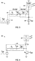
- FIG. 3 is a circuit schematic of another example of a laser emitter circuit 306.
- the circuit is also a resonant LD drive circuit, but the resonant circuit 310 includes a series RLC comprised of resistive circuit element Rs which can be the lumped parasitic resistance along the series RLC tank circuit, capacitive circuit element C DRV arranged in series to the drive signal source 312 that provides the input signal ( V DRV ), and inductive circuit element LDRV arranged in series to CDRV and a cathode of LD 302.
- the resonant LD drive circuit may be coupled to the anode of LD 302.
- the input signal V DRV can be a square wave signal.
- the resonant circuit 310 filters the square wave signal to produce a continuous wave sinusoidal drive signal to drive the LD 302.
- the input signal does not have to be a square wave signal.
- the input signal V DRV to the circuit can have any type of waveform where significant energy of the input signal is present at substantially the resonant frequency of the resonant circuit 310 (e.g., within 10-20% or less of the resonant frequency).
- FIG. 3 shows that the drive signal source 312 and the capacitive circuit element C DRV can be included in an integrated circuit or chip, and the inductive circuit element L DRV and LD 302 can be off-chip components.
- FIG. 3 also shows a bias circuit 308 that can be on-chip and is coupled to the cathode of the LD 302.
- the bias circuit 308 can be a current source that supplies a bias current I B to LD 302 to ensure that the LD 302 remains on for the driving sinusoidal signal from the resonant circuit 310.
- the LD 302 needs a certain minimum amount of threshold current I TH to "turn on" the laser diode for efficient light emission without distortion.
- I may be 1.0-1.5 Amps (1.0-1.5A).
- I B I A + I TH , where I A is the maximal amplitude of the driving sinusoid.
- the typical value for I A can be high (e.g., 3A to 5A).
- the LD 302 can be approximated as a DC voltage source with a typical voltage drop of 2V for example. Given the standard 3.3V supply, the available voltage headroom for the bias circuit 308 is about 1.3V.
- FIG. 4 is a circuit schematic of another example of a laser emitter circuit 406.
- the circuit includes an input signal source V DRV , a resonant circuit 410, and an LD 402 as in FIG. 3.
- FIG. 4 also includes a bias transistor M B of the bias circuit 308 in FIG. 3 , and shows a parasitic inductance LLD.
- the parasitic inductance L LD represents parasitic bonding wire inductances of the anode and cathode of the LD 402 (the parasitic inductances are lumped together to the cathode as L LD in FIG. 4 ).
- the parasitic inductance can be of the order of 0.5 nano-Henrys (0.5nH), which can cause ripples on summing node A in FIG. 4 .
- V ripple can be as high as 1V. This may severely limit the headroom down for the bias circuit to a minimum of 0.3V and modulates the V of the bias transistor M B .
- An approach to resolving the limited headroom issue is to increase the output impedance of the current source of the bias circuit 308 of FIG. 3 . This can be achieved by making the transistor channel length L longer or adding a cascode transistor to the current source. However, such an approach suffers from a parasitic parallel LC tank circuit.
- FIG. 5 is a circuit diagram of the circuit of FIG. 4 to illustrate the formation of the parasitic LC tank circuit.
- the resonant circuit 410 of FIG. 4 is lumped into a sinusoidal current source I LD , and the LD 402 of FIG. 4 is modeled as a DC voltage source with voltage drop V LD .
- the drain-to-source resistance R DS of transistor is shown and all the parasitic capacitance from summing node A to ground in FIG. 4 is lumped together as C PAR .
- FIG. 6 shows the small signal circuit model of FIG. 5 which indicates the extent of the parasitic parallel LC tank circuit of L LD and Cp .
- a higher output resistance R BIAS of the current source of the bias circuit 308 of FIG. 3 means a higher drain-to-source resistance R DS .
- This in turn means a higher quality factor Q of the parasitic parallel LC tank circuit.
- the traditional approach of increasing the output impedance of the bias circuit 308 will boost the Q of the parallel tank.
- the parasitic parallel LC tank circuit generally has a much higher resonant frequency than the main resonant circuit 410 in FIG. 4 , the total harmonic distortion (THD) of the laser diode current I LD in FIGS. 5 and 6 degrades dramatically.
- TDD total harmonic distortion
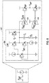
- FIG. 7A is a circuit schematic of another example of a laser emitter circuit 706 to solve the headroom issue of the current source.
- the V DRV drive signal source 312 and the resonant circuit 310 of FIG. 3 are represented by sinusoidal current source I LD in FIG. 7
- the circuit 706 includes the LD 702 and shows the parasitic inductance L LD of the laser diode.
- the bias circuit 308 of FIG. 3 is implemented as a current mirror in FIG. 7A comprised of bias transistor M B and transistor M 0 .
- the gate-to-drain capacitance C GD and gate-to-source capacitance C GS of transistor M B are shown.
- the circuit 706 resolves the issue of the limited headroom for the bias circuit 308 in FIG.
- L B is in series from the summing node A to circuit node B at bias transistor M B .
- Bias inductance L B is much larger than parasitic inductance L LD ( L B >> L LD ) and may be an inductor or may be the parasitic inductance from bonding wires.
- the bias inductance may be either at the top or bottom of the bias transistor, or may be at both the top and bottom of the bias transistor.
- the ratio of the current mirror is intentionally made to be large. In some aspects, ratio of current of the first current mirror leg to current of the second current mirror leg is greater than 100. In certain aspects, the ratio of the currents in the mirror is 400.
- the current in the M B branch may be 4A and the current in the M 0 branch may be 10 milliamps (10mA).
- the large current ratio has two effects. First, the impedance looking into the gate terminal of M 0 becomes a relatively high impedance node because the size of M 0 is very small.
- the large size of M B means a large gate-to-drain capacitance C GD , which effectively makes M B diode connected with R DS ⁇ 2 gm where gm is the transconductance of M B and the factor 2 is due to the capacitive division between C GD and C GS . Because the current through M B is very large, 2 / gm, and consequently R DS , is very small, which greatly attenuates the voltage ripple from circuit node A to circuit node B.
- FIG. 7B is the small signal circuit model of the circuit of FIG. 7A .
- the large Vripple at node A is shielded from M B so that M B sees a reduced Vripple and a relatively stable V DS .
- the bias branch of the current mirror still has a high output impedance that is provided by L B because L B >> L LD , so that the current from the resonant circuit I LD will mostly flow to the laser diode 702 instead of the bias circuit.
- the issue of the parasitic parallel LC tank circuit is also resolved.
- FIG. 8 is a circuit schematic of an example of a driver circuit 812 with tunable amplitude.
- the driver circuit 812 includes a main driver circuit that includes power transistors M TOP , M BOT and a pre-driver circuit that includes inverter buffers 814, 816.
- the circuit 812 can provide the input signal V DRV of FIG. 3 .
- Signals V PRE and V PRE are complementary square waves with rail-to-rail signal swing at the resonant frequency of the resonant circuit 310 of FIG. 3 .
- the signals each drive an inverter buffer 814, 816 that each drive a power transistor M TOP and M BOT to produce the drive signal V DRV input to the resonant circuit.
- inverter buffer 816 draws power from the main circuit supply (e.g., V DD ) whereas inverter buffer 814 draws power from a low dropout voltage regulator circuit LDO 818 that has a tunable output voltage V TOP .
- V DD main circuit supply
- LDO 818 low dropout voltage regulator circuit LDO 818 that has a tunable output voltage V TOP .
- transistor M TOP is an n-type metal oxide semiconductor (NMOS) device, a change in V GATE will translate to a corresponding change in the amplitude of V DRV .
- V DRV the amplitude of V DRV can be tuned by tuning V TOP , the circuit supply to inverter 814, which is much easier to do than to directly tune the main circuit supply.
- Tuning the amplitude of V DRV tunes the amplitude of the continuous wave sinusoidal drive signal output from the resonant circuit. This makes the amplitude of the drive signal of the laser diode (e.g., LD 302 in FIG. 3 ) tunable.
- the voltage V TOP can be tuned by the LDO 818 which is formed by transistors M 1 -M 3 .
- the LDO 818 uses a buffered flipped voltage follower circuit topology.
- Transistor M 2 acts as a source follower so that by changing the gate voltage of M 2 or V SET , voltage V TOP is changed accordingly.
- the circuit feedback loop formed by M 1 and M 3 further reduces the output impedance by the loop gain and increases the sourcing capability.
- the LDO 818 should provide very high instantaneous current in a very short time to charge the gate capacitance of M TOP .
- FIG. 9 is an illustration of waveform V PRE which drives inverter buffer 814 and waveform I TOP which is the current supplied to inverter buffer 814 from LDO 818.
- the waveform I TOP is a representation of the desired high instantaneous current to charge the gate capacitance of M TOP . This instantaneous current could be provided by a large off-chip capacitor but adding a bulky external circuit component is undesirable.
- the LDO 818 only needs to provide charge at a transition (e.g., the falling edge) of V P as shown in FIG. 9 .
- an assistive pull up can be added to the LDO 818. This pull up is provided pull up transistor M A which is coupled to the output of the LDO 818 and is controlled by V P .
- FIG. 10 shows an example of a pulse generator circuit 1020 that can generate the control signal V P for pull up transistor M A from signal V PRE , and also shows waveforms associated with the operation of the circuit 1020.
- V P is a negative pulse that only turns transistor M A "on" during the falling edge of V PRE , so that the majority of the charge provided to the gate capacitance of M TOP is provided by the assistive path from transistor M A .
- the control signal V P can be a negative pulse generated using the circuit 1020, and the pulse width tp of the negative pulse can be adjusted by the delay chain in the pulse generator circuit 1020 to optimize for the best pull up timing.
- the pulse width of the V DRV signal can be adjustable by the drive circuit (e.g., the duty cycle can be changed to something other than a 50:50 duty cycle). This may be useful to reduce the harmonic content of the continuous wave signal that drives the laser diode or allow for pre-distortion of the continuous wave signal.
- the amplitude of the V DRV signal can be adjusted by the driver circuit to provide a multi-level drive signal.
- the drive circuit may include a digital-to-analog converter (DAC) circuit to set the level of the V DRV signal.
- the DAC circuit may include a number of bits (e.g., 2-3 bits) to set the signal level. This may also be useful to reduce harmonic content. It may also reduce the Q needed for the resonator circuit. It may also reduce the need for accuracy of the resonant frequency of the resonant circuit.
- the drive circuit and the LDO 818 of FIG. 8 can be included on an integrated circuit (IC) with the capacitive circuit element of the resonant circuit.
- the inductive circuit element can be integrated in the IC, can be a discrete inductor, or can be bonding wire inductance.
- the bias circuit can also be included on the IC, while the laser diode is external to the IC.
- the amplitude tuning with the tunable LDO and pull up assist reduces the number of large off-chip components needed to drive the laser diode.
- Other options for generating one or both of the drive supply voltage and the pre-drive supply voltage are possible (e.g., using linear or switched mode power supplies).
- the resonant frequency ⁇ 0 of the resonant circuit 310 should match the frequency of the input signal V DRV .
- variation in the inductance and capacitance of LDRV and C DRV can shift ⁇ 0 and degrade performance of the laser diode driver.
- the resonant circuit 310 is helpful for the resonant circuit 310 to be adjustable to tune the resonant frequency ⁇ 0 substantially to the frequency of the input drive signal V DRV (e.g., to within 1% or less of the frequency of the input drive signal or within 10% or less of the frequency of the input drive signal).
- One way to make the resonant circuit tunable is to make the capacitive circuit element C DRV a tunable capacitance circuit.
- FIG. 11 is circuit schematic of another example of a laser emitter circuit 1106.
- the laser emitter circuit includes a resonant circuit 1110 that includes a tunable capacitance circuit 1122.
- the tunable capacitance circuit 1122 includes a tunable bank of capacitive circuit elements that are enabled into the resonant circuit using one or more switches.
- the tunable capacitance circuit 1122 has a 4-bit resolution corresponding to four switches coupled to capacitance values that are binary-weighted.
- the overall capacitance of the tunable capacitance circuit 1122 can be changed by turning on any combination of zero to four switches to set the capacitance.
- the resonant frequency ⁇ 0 of the resonant circuit 110 can be tuned so that, in the worst case, the mismatch between ⁇ 0 and the frequency of V DRV is 1.25%.
- the tunable capacitance circuit 1122 provides discrete fine tuning of capacitance that can overcome ⁇ 20% variation in resonant frequency ⁇ 0 . Further, the tuning technique can be extended to allow setting the ⁇ 0 of the resonant circuit 1110 to multiple operating frequencies by introducing extra switchable capacitive banks or separate drive circuits as described below.
- the switches of the tunable capacitance circuit are implemented with NMOS devices whose parasitics can play an important role in determining the realized value of ⁇ 0 .
- the NMOS switch device should be sized to minimize the on-resistance R ON of the switch.
- this typically means making the switch larger which results in a significant amount of drain-to-bulk capacitance C DB , drain-to-source capacitance C DS , and source-to-bulk capacitance C SB . This can affect the overall capacitance of the tunable capacitance circuit 1122.
- FIG. 12 is a circuit schematic of a resonant circuit 1210 including an equivalent circuit model of one switch of the tunable bank of capacitive circuit elements, and the capacitance C sw switched into the circuit by the switch.
- C sw is in series with C DS and C SB .
- This means there is an effective capacitance C EFF of C EFF C SW C SB + C DS C SW + C SB + C DS when the switch is off, as opposed to a capacitance of zero for an ideal switch.
- This off capacitance can be compensated for by properly choosing capacitance values so that C SW dominates the series combination of capacitance.
- the switch transistor should be a high voltage device because when the switch is off, a high V DS is dropped across the off switch.
- FIG. 13 is a circuit schematic of another example of a laser emitter circuit 1306. Similar to the example of FIG. 3 , the laser emitter circuit 1306 includes a resonant circuit 1310. A difference from the resonant circuit of FIG. 3 is that the resonant circuit 1310 is coupled to the anode of the LD 1302. The laser emitter circuit 1306 also shows a bias inductance L BIAS that is also coupled to the anode of LD 1302. Capacitor C LSR is parasitic capacitance of the laser diode.
- the resonant circuit 1310 includes a series RLC tank circuit comprised of resistive circuit element R DRV , capacitive circuit element C DRV , and inductive circuit element L DRV arranged in series.
- V DRV can be a square wave signal and the resonant circuit filters the square wave input signal to produce a continuous wave sinusoidal drive signal to drive the laser diode.
- Resistive circuit element R DRV can be the lumped parasitic resistance of the circuit used to generate the V DRV signal and the parasitic resistance along the series RLC tank circuit.
- C DRV and L DRV can be passive circuit components external to an integrated circuit that includes the driver circuit that generates V DRV .
- L DRV can include parasitic inductance (e.g., from bond wires) in the circuit loop that includes the driver circuit, the resonant circuit 1310, and the LD 1302.
- FIG. 14 is a circuit schematic of another example of a laser emitter circuit 1406.
- the circuit 1406 includes a resonant circuit 1410 coupled to the anode of the LD 1402.
- the resonant circuit 1410 includes capacitive circuit element C DRV and inductive circuit element L DRV and filters the input signal V DRV to produce a continuous wave sinusoidal drive signal to drive the LD 1402.
- a bias circuit 1408 can be a current source that supplies a bias current I B to LD 1402 to ensure that the LD 1402 remains on for the driving sinusoidal signal.
- the circuit 1406 includes bias inductance L B in series from bias node B to the summing node A, and bias capacitance C B .
- Bias capacitance C B reduces the impedance on bias node B to avoid a high Vripple on node B that could be seen by the bias circuit 1408.
- the bias circuit 1408, driver circuit that generates V DRV , and capacitive circuit element C DRV can be included on an IC 1424.
- the capacitance of C DRV is made much larger than the load capacitance seen by the resonant circuit 1410 which includes parasitic capacitance C PAR of LD 1402.
- Bias inductance L B is made larger than inductive circuit element L DRV .
- One or both of L DRV and LB can be the parasitic inductance of bonding wire used in the laser emitter circuit 1406.
- the driver amplitude of V DRV could be controlled by altering the supply voltage to the driver, or by altering the supply voltage to the pre-driver within the circuit.
- the supply voltage could come from a linear regulator or from a switch mode regulator.
- FIG. 15 is an illustration of using bonding wires to form circuit inductances.
- the bonding wires are arranged at the IC of the laser diode 1502.
- Bias inductance L B can be formed using a larger looped bond wire to make the higher inductance to make a higher impedance on the bias line of the circuit.
- Inductance L DRV of the resonant circuit 1410 of FIG. 4 can be formed from multiple parallel short bond wires to form a lower inductance and the dominant (lower) impedance.
- FIG. 16 is a circuit schematic of another example of a laser emitter circuit 1606. It may be useful to have multiple drive paths in a laser emitter circuit to provide the option to drive the laser diode with one of multiple drive signals.
- the example of FIG. 16 includes two drive paths for LD 1602. One drive path applies drive signal V DRV1 having a higher frequency (e.g., 200MHz), and the other drive path applies drive signal V DRV2 having a lower frequency (e.g., .
- Each of the drive paths includes a resonant circuit 1610, 1630 to filter the drive signal to provide a continuous wave sinusoidal signal to the LD 1602.
- the drive signals V DRV1 and V DRV2 are square wave signals.
- the drive signals can be enabled to its corresponding resonant circuit using a high impedance or tristate-able driver 1632.
- the circuit also includes a bias circuit comprised of current source I B , bias inductance L B , and bypass capacitance C B as in the example of FIG. 14 .
- Resonant circuit 1610 includes C DRV1 and L DRV1 .
- Resonant circuit 1630 includes C DRV2 and L DRV2 .
- the capacitance of C DRV1 is made much larger than the load capacitance seen by the resonant circuit 1610 which includes parasitic capacitance C PAR of LD 1602.
- the capacitance of C DRV2 is made larger than C DRV1 , and the inductance L DRV2 is larger than L DRV1 .
- Capacitances C DRV1 and C DRV2 may be fine-tunable capacitance circuits to tune the resonant frequencies ⁇ 01 , ⁇ 02 of the resonant paths to the frequencies of its corresponding drive signal.
- Multiple drive paths with multiple resonant circuits may be a desirable alternative to changing the resonant frequency by using tunable capacitance or inductance circuits when the difference between the resonant frequency of the two drive signals is large.
- the capacitance C DRV would need to change by 16 times.
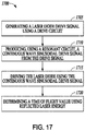
- FIG. 17 is a flow diagram of an example of a method 1700 of operating a ToF sensor.
- a drive signal is generated using a drive circuit.
- the drive signal may be a square wave, and the drive circuit may tunable amplitude such as the drive circuit 812 of FIG. 8 .
- a continuous wave sinusoidal drive signal is produced from the drive signal using a resonant circuit.
- the resonant circuit may be any of the resonant circuits described herein.
- the laser diode is driven using the continuous wave sinusoidal drive signal to activate the laser diode.
- the activation may cause the laser diode to emit a continuous sinusoidal wave of laser energy.
- the emitted laser energy can reflect off an object.
- Reflected laser energy can be detected by the ToF sensor (e.g., using a photo diode) and at 1720 the detected reflected laser energy can be used to determine a distance to an object, such as by the method described herein in regard to FIG. 1 .
- the devices systems and methods provide a highly integrated, low cost solution for driving an LD with a low total harmonic distortion (THD) sinusoidal signal with tunable amplitude and frequency.
- TDD total harmonic distortion
- a first Aspect includes subject matter (such as a laser emitter circuit) comprising a laser diode, a driver circuit configured to generate a drive signal, and a resonant circuit coupled to the driver circuit and the laser diode, wherein the resonant circuit is configured to use the drive signal of the driver circuit to generate a continuous wave sinusoidal drive signal to drive the laser diode.
- subject matter such as a laser emitter circuit
- a driver circuit configured to generate a drive signal
- a resonant circuit coupled to the driver circuit and the laser diode, wherein the resonant circuit is configured to use the drive signal of the driver circuit to generate a continuous wave sinusoidal drive signal to drive the laser diode.
- the subject matter of Aspect 1 optionally includes a bias circuit coupled to the laser diode, and the driver circuit is optionally configured to generate a drive signal with significant energy at substantially a resonant frequency of the resonant circuit.
- the resonant circuit is configured to produce the continuous wave sinusoidal drive signal from the drive signal and includes a capacitive circuit element coupled in series to the drive circuit, and an inductive circuit element arranged in series to the capacitive circuit element and the laser diode.
- the subject matter of Aspect 2 optionally includes a driver circuit configured to generate a square wave drive signal and the resonant circuit is configured to produce the continuous wave sinusoidal drive signal from the square wave drive signal.
- Aspect 4 the subject matter of one or any combination of Aspects 1-3 optionally includes an amplitude tuning circuit configured to adjust a circuit supply of the driver circuit to adjust an amplitude of continuous wave sinusoidal drive signal.
- the subject matter of Aspect 4 optionally includes a pre-driver circuit that includes a buffer circuit to provide a square wave drive signal as the drive signal, and an amplitude tuning circuit that includes a voltage regulator circuit with a tunable output voltage provided as a circuit supply to the buffer circuit.
- Aspect 6 the subject matter of Aspect 5 optionally includes an amplitude tuning circuit that includes a pull up assist transistor coupled to an output of the voltage regulator circuit, wherein the pull up assist transistor is only activated during a transition of an input signal to the buffer circuit.
- the subject matter of one or any combination of Aspects 1-6 optionally includes a bias circuit coupled to one of a cathode or an anode of the laser diode.
- the bias circuit includes a bias inductance coupled to the laser diode and a current mirror coupled to bias inductance.
- Aspect 8 the subject matter of one or any combination of Aspects 1-7 optionally includes a resonant circuit tunable to adjust a resonant frequency of the resonant circuit to a frequency of the drive signal.
- Aspect 9 the subject matter of Aspect 8 optionally includes a tunable capacitance circuit.
- the subject matter of Aspect 9 optionally includes a tunable capacitance circuit includes multiple capacitive circuit elements and at least one switch circuit, and wherein a capacitive circuit element coupled to the at least one switch circuit is greater than the parasitic capacitances of the switch circuit when the switch circuit is in an off state.
- Aspect 11 includes subject matter (such as a laser diode drive circuit) or can be combined with one or any combination of Aspects 1-10 to include such subject matter, comprising a driver circuit configured to generate a drive signal, a resonant circuit, and a bias circuit.
- the resonant circuit has an input coupled to an output of the driver circuit and has an output for coupling to a laser diode.
- the resonant circuit is configured to produce a continuous wave sinusoidal drive signal from the drive signal to drive the laser diode.
- the bias circuit includes a bias inductance for coupling to the laser diode.
- the subject matter of Aspect 11 optionally includes a bias circuit including a current mirror circuit including a first current mirror branch and a second current mirror branch, wherein the first current mirror branch is coupled to the bias inductance.
- the subject matter of one or both of Aspect 11 and 12 optionally includes the laser diode.
- the resonant circuit optionally includes a capacitive circuit element coupled in series to the driver circuit and an inductive circuit element arranged in series to the capacitive circuit element and the cathode of the laser diode.
- Aspect 14 the subject matter of one or any combination of Aspects 11-13 optionally includes a resonant circuit tunable to adjust a resonant frequency of the resonant circuit to a frequency of the drive signal.
- Aspect 15 the subject matter of one or any combination of Aspects 11-14 optionally includes a resonant circuit that includes an inductive circuit element, and at least one of the bias inductance or the inductive circuit element of the resonant circuit is implemented using one or more bond wires of an integrated circuit that includes the laser diode.
- the subject matter of one or any combination of Aspects 11-15 optionally includes an amplitude tuning circuit configured to adjust a circuit supply of the driver circuit to adjust an amplitude of continuous wave sinusoidal drive signal.
- the subject matter of Aspect 16 optionally includes an amplitude tuning circuit that includes a voltage regulator circuit having a tunable output voltage provided as a circuit supply to the driver circuit.
- the subject matter of one or any combination of Aspects 11-17 optionally includes a second drive circuit configured to generate a second drive signal and a second resonant circuit coupled to the second drive circuit and having an output for coupling to the laser diode, wherein the second resonant circuit is configured to produce a second continuous wave sinusoidal drive signal from the second drive signal to drive the laser diode.
- Aspect 19 includes subject matter (such as a method of operating a laser emitter of a time of flight sensor) or can optionally be combined with one or any combination of Aspects 1-18 to include such subject matter, comprising generating a drive signal using a driver circuit, producing, using a resonant circuit, a continuous wave sinusoidal drive signal from the square wave drive signal, and driving the laser diode using the continuous wave sinusoidal drive signal.
- the subject matter of Aspect 19 optionally includes biasing the operating current of the laser diode using a bias inductance coupled to the laser diode and a current mirror coupled to the bias inductor.
- the subject matter of one or both of Aspects 19 and 20 optionally includes a driver circuit includes a pre-driver circuit and a main driver circuit, and adjusting a circuit supply of one or both of the pre-driver circuit and the main driver circuit to adjust the amplitude of the continuous wave sinusoidal drive signal.
- the subject matter of one or any combination of Aspects 19-21 optionally includes tuning the resonant frequency of the resonant circuit to the frequency of the drive signal.
Landscapes
- Physics & Mathematics (AREA)
- General Physics & Mathematics (AREA)
- Condensed Matter Physics & Semiconductors (AREA)
- Electromagnetism (AREA)
- Optics & Photonics (AREA)
- Engineering & Computer Science (AREA)
- Computer Networks & Wireless Communication (AREA)
- Radar, Positioning & Navigation (AREA)
- Remote Sensing (AREA)
- Semiconductor Lasers (AREA)
Abstract
Description
- This document relates generally to electronic circuits for optical applications, and in particular it relates to electronic circuits that include a laser emitting diode.
- Time-of-flight (ToF) is a technique for three-dimensional (3D) imaging. The technique illuminates the object with a modulated light and receives reflected light. Based on the modulating frequency and the phase difference between the transmitted and received light, the distance between the camera and the object can be calculated. This phase shift can be detected either using a pulsed approach or a continuous-wave (CW) approach. The CW approach traditionally uses a square wave because it is easily realizable using digital circuits. However, a square wave output is less efficient than using a sinusoidal wave, and using a square wave also suffers from the harmonic contents that impose difficulty in depth calibration. Because of the lack of harmonics, using a sinusoidal wave provides better depth performance but the generation of a sinusoid also presents challenges in the driver design.
- This document relates generally to driver circuits for laser diodes and methods of their operation. A laser emitter circuit according to various aspects includes a laser diode; a driver circuit configured to generate a drive signal; and a resonant circuit coupled to the driver circuit and the laser diode, wherein the resonant circuit is configured to use the drive signal of the driver circuit to generate a continuous wave sinusoidal drive signal to drive the laser diode.
- A laser diode drive circuit according to various aspects includes a driver circuit configured to generate a drive signal; a resonant circuit having an input coupled to an output of the driver circuit and having an output for coupling to a laser diode, wherein the resonant circuit is configured to produce a continuous wave sinusoidal drive signal from the drive signal to drive the laser diode; and a bias circuit including a bias inductance for coupling to the laser diode.
- A method of operating a time of flight sensor according to various aspects includes generating a drive signal using a drive circuit; producing, using a resonant circuit, a continuous wave sinusoidal drive signal from the drive signal; and driving the laser diode using the continuous wave sinusoidal drive signal.
- This section is intended to provide an overview of subject matter of the present patent application. It is not intended to provide an exclusive or exhaustive explanation of the invention. The detailed description is included to provide further information about the present patent application.
- In the drawings, which are not necessarily drawn to scale, like numerals may describe similar components in different views. Like numerals having different letter suffixes may represent different instances of similar components. The drawings illustrate generally, by way of example, but not by way of limitation, various embodiments discussed in the present document.
-
FIG. 1 is an illustration of an example of a time of flight (ToF) sensor. -
FIG. 2 is a circuit schematic of an example of a laser emitter circuit for a ToF sensor. -
FIG. 3 is a circuit schematic of another example of a laser emitter circuit. -
FIG. 4 is a circuit schematic of another example of a laser emitter circuit. -
FIG. 5 is another circuit schematic of the example circuit ofFIG. 4 . -
FIG. 6 shows the small signal circuit model of the example circuit ofFIG. 5 . -
FIG. 7A is a circuit schematic of another example of a laser emitter circuit. -
FIG. 7B is the small signal circuit model of the circuit ofFIG. 7A . -
FIG. 8 is a circuit schematic of an example of an implementation of a drive signal generator circuit. -
FIGS. 9-10 are illustrations of waveforms associated with operation of the circuit ofFIG. 8 . -
FIG. 11 is circuit schematic of another example of a laser emitter circuit. -
FIG. 12 is a circuit schematic of an example of a resonant circuit. -
FIG. 13 is circuit schematic of another example of a laser emitter circuit. -
FIG. 14 is circuit schematic of another example of a laser emitter circuit. -
FIG. 15 is an illustration of examples of using bonding wires to form circuit inductances. -
FIG. 16 is a circuit schematic of another example of a laser emitter circuit. -
FIG. 17 is a flow diagram of an example of a method of operating a ToF sensor. -
FIG. 1 is an illustration of an example of a time-of-flight (ToF) sensor. TheToF sensor 100 includes an emitter and a receiver. The emitter can include alaser diode 102 that converts electrical current to light energy. The receiver can be aphoto diode 104 that converts received light energy into electrical current or voltage. - To obtain depth information for imaging, the laser emitter may send a laser pulse to the object and the receiver detects the reflected laser energy including phase information. A timer is started when the emitter sends out a light pulse and the timer is stopped when a pulse reflected from an object is received at the ToF sensor. Based on the time it takes for the pulse to do the round trip (treceive - temit) and the speed of light c, the depth information d of the object can be calculated as

laser diode 102 with a square wave, but using a square wave is inefficient and suffers from the harmonic contents that impose difficulty in depth calibration. -
FIG. 2 is a circuit schematic of an example of alaser emitter circuit 206 for a ToF sensor. The circuit is a resonant laser diode (LD) driver. The LD 202 may be a vertical cavity surface emitting laser (VCSEL) diode or an edge emitting laser (EEL) diode. The inductors L and the capacitor C form a resonant LC circuit that resonates when the transistor M is activated. The ringing of the LC circuit drives theLD 202 with a continuous wave (CW) signal. The inductors L may be the parasitic inductance of bonding wires. This approach takes advantage of the bonding wire inductance rather than using discrete inductors and trying to minimize the bonding wire inductance. However, the values of inductance and capacitance need to be tuned to the implementation. -
FIG. 3 is a circuit schematic of another example of alaser emitter circuit 306. The circuit uses a 3.3Volt supply (VDD = 3.3V) to facilitate system integration. The circuit is also a resonant LD drive circuit, but theresonant circuit 310 includes a series RLC comprised of resistive circuit element Rs which can be the lumped parasitic resistance along the series RLC tank circuit, capacitive circuit element C DRV arranged in series to thedrive signal source 312 that provides the input signal (VDRV ), and inductive circuit element LDRV arranged in series to CDRV and a cathode ofLD 302. In variations, the resonant LD drive circuit may be coupled to the anode ofLD 302. The input signal VDRV can be a square wave signal. Theresonant circuit 310 filters the square wave signal to produce a continuous wave sinusoidal drive signal to drive theLD 302. The input signal does not have to be a square wave signal. The input signal VDRV to the circuit can have any type of waveform where significant energy of the input signal is present at substantially the resonant frequency of the resonant circuit 310 (e.g., within 10-20% or less of the resonant frequency). -
FIG. 3 shows that thedrive signal source 312 and the capacitive circuit element CDRV can be included in an integrated circuit or chip, and the inductive circuit element LDRV andLD 302 can be off-chip components.FIG. 3 also shows abias circuit 308 that can be on-chip and is coupled to the cathode of theLD 302. - The
bias circuit 308 can be a current source that supplies a bias current IB toLD 302 to ensure that theLD 302 remains on for the driving sinusoidal signal from theresonant circuit 310. TheLD 302 needs a certain minimum amount of threshold current ITH to "turn on" the laser diode for efficient light emission without distortion. For example, I may be 1.0-1.5 Amps (1.0-1.5A). Because the current driving theLD 302 is sinusoidal, to avoid dipping below ITH , the minimal bias current of LD is given by
LD 302 can be approximated as a DC voltage source with a typical voltage drop of 2V for example. Given the standard 3.3V supply, the available voltage headroom for thebias circuit 308 is about 1.3V. -
FIG. 4 is a circuit schematic of another example of alaser emitter circuit 406. The circuit includes an input signal source VDRV , aresonant circuit 410, and anLD 402 as inFIG. 3. FIG. 4 also includes a bias transistor MB of thebias circuit 308 inFIG. 3 , and shows a parasitic inductance LLD. The parasitic inductance LLD represents parasitic bonding wire inductances of the anode and cathode of the LD 402 (the parasitic inductances are lumped together to the cathode as LLD inFIG. 4 ). The parasitic inductance can be of the order of 0.5 nano-Henrys (0.5nH), which can cause ripples on summing node A inFIG. 4 . The ripple amplitude is given by
- An approach to resolving the limited headroom issue is to increase the output impedance of the current source of the
bias circuit 308 ofFIG. 3 . This can be achieved by making the transistor channel length L longer or adding a cascode transistor to the current source. However, such an approach suffers from a parasitic parallel LC tank circuit. -
FIG. 5 is a circuit diagram of the circuit ofFIG. 4 to illustrate the formation of the parasitic LC tank circuit. Theresonant circuit 410 ofFIG. 4 is lumped into a sinusoidal current source ILD, and theLD 402 ofFIG. 4 is modeled as a DC voltage source with voltage drop VLD. Also, the drain-to-source resistance RDS of transistor is shown and all the parasitic capacitance from summing node A to ground inFIG. 4 is lumped together as CPAR. -
FIG. 6 shows the small signal circuit model ofFIG. 5 which indicates the extent of the parasitic parallel LC tank circuit of LLD and Cp . A higher output resistance RBIAS of the current source of thebias circuit 308 ofFIG. 3 means a higher drain-to-source resistance RDS . This in turn means a higher quality factor Q of the parasitic parallel LC tank circuit. The traditional approach of increasing the output impedance of thebias circuit 308 will boost the Q of the parallel tank. As the parasitic parallel LC tank circuit generally has a much higher resonant frequency than the mainresonant circuit 410 inFIG. 4 , the total harmonic distortion (THD) of the laser diode current ILD inFIGS. 5 and 6 degrades dramatically. -
FIG. 7A is a circuit schematic of another example of alaser emitter circuit 706 to solve the headroom issue of the current source. The VDRVdrive signal source 312 and theresonant circuit 310 ofFIG. 3 are represented by sinusoidal current source ILD inFIG. 7 , and thecircuit 706 includes theLD 702 and shows the parasitic inductance LLD of the laser diode. Thebias circuit 308 ofFIG. 3 is implemented as a current mirror inFIG. 7A comprised of bias transistor MB and transistor M 0. The gate-to-drain capacitance CGD and gate-to-source capacitance CGS of transistor MB are shown. Thecircuit 706 resolves the issue of the limited headroom for thebias circuit 308 inFIG. 3 by including a bias inductance LB in the bias circuit. In the example ofFIG. 7A , LB is in series from the summing node A to circuit node B at bias transistor MB. Bias inductance LB is much larger than parasitic inductance LLD (LB >> LLD ) and may be an inductor or may be the parasitic inductance from bonding wires. The bias inductance may be either at the top or bottom of the bias transistor, or may be at both the top and bottom of the bias transistor. - The ratio of the current mirror is intentionally made to be large. In some aspects, ratio of current of the first current mirror leg to current of the second current mirror leg is greater than 100. In certain aspects, the ratio of the currents in the mirror is 400. For example, the current in the MB branch may be 4A and the current in the M 0 branch may be 10 milliamps (10mA). The large current ratio has two effects. First, the impedance looking into the gate terminal of M 0 becomes a relatively high impedance node because the size of M 0 is very small. Second, the large size of MB means a large gate-to-drain capacitance CGD, which effectively makes MB diode connected with

factor 2 is due to the capacitive division between CGD and CGS . Because the current through MB is very large, 2/gm, and consequently RDS , is very small, which greatly attenuates the voltage ripple from circuit node A to circuit node B. -
FIG. 7B is the small signal circuit model of the circuit ofFIG. 7A . As shown inFIG. 7B , the large Vripple at node A is shielded from MB so that MB sees a reduced Vripple and a relatively stable VDS. However, the bias branch of the current mirror still has a high output impedance that is provided by LB because LB >> LLD, so that the current from the resonant circuit ILD will mostly flow to thelaser diode 702 instead of the bias circuit. The issue of the parasitic parallel LC tank circuit is also resolved. The added inductance LB together with the small RDS (= 2/gm) of the parasitic tank circuit greatly reduces the Q of the parasitic tank circuit from
- The amplitude of the laser diode drive current is

FIG. 8 is a circuit schematic of an example of adriver circuit 812 with tunable amplitude. Thedriver circuit 812 includes a main driver circuit that includes power transistors MTOP , MBOT and a pre-driver circuit that includes inverter buffers 814, 816. Thecircuit 812 can provide the input signal VDRV ofFIG. 3 . Signals VPRE andVPRE are complementary square waves with rail-to-rail signal swing at the resonant frequency of theresonant circuit 310 ofFIG. 3 . The signals each drive aninverter buffer - Both power transistors act as switches to generate a square wave signal. However,
inverter buffer 816 draws power from the main circuit supply (e.g., VDD) whereasinverter buffer 814 draws power from a low dropout voltageregulator circuit LDO 818 that has a tunable output voltage VTOP. This causes the output VGA of inverter 813 to also have tunable amplitude according to VTOP. Because transistor MTOP is an n-type metal oxide semiconductor (NMOS) device, a change in VGATE will translate to a corresponding change in the amplitude of VDRV. In this way, the amplitude of VDRV can be tuned by tuning VTOP, the circuit supply toinverter 814, which is much easier to do than to directly tune the main circuit supply. Tuning the amplitude of VDRV tunes the amplitude of the continuous wave sinusoidal drive signal output from the resonant circuit. This makes the amplitude of the drive signal of the laser diode (e.g.,LD 302 inFIG. 3 ) tunable. - The voltage VTOP can be tuned by the
LDO 818 which is formed by transistors M1-M3. The LDO 818 uses a buffered flipped voltage follower circuit topology. Transistor M2 acts as a source follower so that by changing the gate voltage of M2 or VSET, voltage VTOP is changed accordingly. The circuit feedback loop formed by M1 and M3 further reduces the output impedance by the loop gain and increases the sourcing capability. In practice, theLDO 818 should provide very high instantaneous current in a very short time to charge the gate capacitance of MTOP. -
FIG. 9 is an illustration of waveform VPRE which drivesinverter buffer 814 and waveform ITOP which is the current supplied toinverter buffer 814 fromLDO 818. The waveform ITOP is a representation of the desired high instantaneous current to charge the gate capacitance of MTOP. This instantaneous current could be provided by a large off-chip capacitor but adding a bulky external circuit component is undesirable. It should be noted that theLDO 818 only needs to provide charge at a transition (e.g., the falling edge) of VP as shown inFIG. 9 . To avoid using a large off-chip capacitor, an assistive pull up can be added to theLDO 818. This pull up is provided pull up transistor MA which is coupled to the output of theLDO 818 and is controlled by VP. -
FIG. 10 shows an example of apulse generator circuit 1020 that can generate the control signal VP for pull up transistor MA from signal VPRE , and also shows waveforms associated with the operation of thecircuit 1020. As shown inFIG. 10 , VP is a negative pulse that only turns transistor MA "on" during the falling edge of VPRE , so that the majority of the charge provided to the gate capacitance of MTOP is provided by the assistive path from transistor MA. The control signal VP can be a negative pulse generated using thecircuit 1020, and the pulse width tp of the negative pulse can be adjusted by the delay chain in thepulse generator circuit 1020 to optimize for the best pull up timing. - In certain aspects, the pulse width of the VDRV signal can be adjustable by the drive circuit (e.g., the duty cycle can be changed to something other than a 50:50 duty cycle). This may be useful to reduce the harmonic content of the continuous wave signal that drives the laser diode or allow for pre-distortion of the continuous wave signal. In certain aspects, the amplitude of the VDRV signal can be adjusted by the driver circuit to provide a multi-level drive signal. For example, the drive circuit may include a digital-to-analog converter (DAC) circuit to set the level of the VDRV signal. The DAC circuit may include a number of bits (e.g., 2-3 bits) to set the signal level. This may also be useful to reduce harmonic content. It may also reduce the Q needed for the resonator circuit. It may also reduce the need for accuracy of the resonant frequency of the resonant circuit.
- The drive circuit and the
LDO 818 ofFIG. 8 can be included on an integrated circuit (IC) with the capacitive circuit element of the resonant circuit. The inductive circuit element can be integrated in the IC, can be a discrete inductor, or can be bonding wire inductance. The bias circuit can also be included on the IC, while the laser diode is external to the IC. Thus, the amplitude tuning with the tunable LDO and pull up assist reduces the number of large off-chip components needed to drive the laser diode. Other options for generating one or both of the drive supply voltage and the pre-drive supply voltage are possible (e.g., using linear or switched mode power supplies). - Returning to
FIG. 3 , the resonant frequency ω 0 of theresonant circuit 310 should match the frequency of the input signal VDRV. However, variation in the inductance and capacitance of LDRV and CDRV can shift ω 0 and degrade performance of the laser diode driver. It is helpful for theresonant circuit 310 to be adjustable to tune the resonant frequency ω 0 substantially to the frequency of the input drive signal VDRV (e.g., to within 1% or less of the frequency of the input drive signal or within 10% or less of the frequency of the input drive signal). One way to make the resonant circuit tunable is to make the capacitive circuit element CDRV a tunable capacitance circuit. -
FIG. 11 is circuit schematic of another example of alaser emitter circuit 1106. The laser emitter circuit includes aresonant circuit 1110 that includes atunable capacitance circuit 1122. Thetunable capacitance circuit 1122 includes a tunable bank of capacitive circuit elements that are enabled into the resonant circuit using one or more switches. In the example ofFIG. 11 , thetunable capacitance circuit 1122 has a 4-bit resolution corresponding to four switches coupled to capacitance values that are binary-weighted. The overall capacitance of thetunable capacitance circuit 1122 can be changed by turning on any combination of zero to four switches to set the capacitance. By changing the capacitance, the resonant frequency ω 0 of the resonant circuit 110 can be tuned so that, in the worst case, the mismatch between ω 0 and the frequency of VDRV is 1.25%. Thetunable capacitance circuit 1122 provides discrete fine tuning of capacitance that can overcome ±20% variation in resonant frequency ω 0. Further, the tuning technique can be extended to allow setting the ω 0 of theresonant circuit 1110 to multiple operating frequencies by introducing extra switchable capacitive banks or separate drive circuits as described below. - In practice, the switches of the tunable capacitance circuit are implemented with NMOS devices whose parasitics can play an important role in determining the realized value of ω 0. The NMOS switch device should be sized to minimize the on-resistance RON of the switch. However, this typically means making the switch larger which results in a significant amount of drain-to-bulk capacitance CDB , drain-to-source capacitance CDS , and source-to-bulk capacitance CSB . This can affect the overall capacitance of the
tunable capacitance circuit 1122. -
FIG. 12 is a circuit schematic of aresonant circuit 1210 including an equivalent circuit model of one switch of the tunable bank of capacitive circuit elements, and the capacitance C sw switched into the circuit by the switch. When a switch is an off state, C sw is in series with CDS and CSB . This means there is an effective capacitance CEFF of
-
FIG. 13 is a circuit schematic of another example of alaser emitter circuit 1306. Similar to the example ofFIG. 3 , thelaser emitter circuit 1306 includes a resonant circuit 1310. A difference from the resonant circuit ofFIG. 3 is that the resonant circuit 1310 is coupled to the anode of theLD 1302. Thelaser emitter circuit 1306 also shows a bias inductance LBIAS that is also coupled to the anode ofLD 1302. Capacitor CLSR is parasitic capacitance of the laser diode. - The resonant circuit 1310 includes a series RLC tank circuit comprised of resistive circuit element RDRV , capacitive circuit element CDRV , and inductive circuit element LDRV arranged in series. VDRV can be a square wave signal and the resonant circuit filters the square wave input signal to produce a continuous wave sinusoidal drive signal to drive the laser diode. Resistive circuit element RDRV can be the lumped parasitic resistance of the circuit used to generate the VDRV signal and the parasitic resistance along the series RLC tank circuit. CDRV and LDRV can be passive circuit components external to an integrated circuit that includes the driver circuit that generates VDRV. LDRV can include parasitic inductance (e.g., from bond wires) in the circuit loop that includes the driver circuit, the resonant circuit 1310, and the
LD 1302. -
FIG. 14 is a circuit schematic of another example of alaser emitter circuit 1406. Thecircuit 1406 includes a resonant circuit 1410 coupled to the anode of theLD 1402. The resonant circuit 1410 includes capacitive circuit element CDRV and inductive circuit element LDRV and filters the input signal VDRV to produce a continuous wave sinusoidal drive signal to drive theLD 1402. Abias circuit 1408 can be a current source that supplies a bias current IB toLD 1402 to ensure that theLD 1402 remains on for the driving sinusoidal signal. Thecircuit 1406 includes bias inductance LB in series from bias node B to the summing node A, and bias capacitance CB . Bias capacitance CB reduces the impedance on bias node B to avoid a high Vripple on node B that could be seen by thebias circuit 1408. In the example ofFIG. 14 , thebias circuit 1408, driver circuit that generates VDRV , and capacitive circuit element CDRV can be included on an IC 1424. The capacitance of CDRV is made much larger than the load capacitance seen by the resonant circuit 1410 which includes parasitic capacitance CPAR ofLD 1402. Bias inductance LB is made larger than inductive circuit element LDRV. One or both of LDRV and LB can be the parasitic inductance of bonding wire used in thelaser emitter circuit 1406. The driver amplitude of VDRV could be controlled by altering the supply voltage to the driver, or by altering the supply voltage to the pre-driver within the circuit. The supply voltage could come from a linear regulator or from a switch mode regulator. -
FIG. 15 is an illustration of using bonding wires to form circuit inductances. The bonding wires are arranged at the IC of thelaser diode 1502. Bias inductance LB can be formed using a larger looped bond wire to make the higher inductance to make a higher impedance on the bias line of the circuit. Inductance LDRV of the resonant circuit 1410 ofFIG. 4 can be formed from multiple parallel short bond wires to form a lower inductance and the dominant (lower) impedance. -
FIG. 16 is a circuit schematic of another example of alaser emitter circuit 1606. It may be useful to have multiple drive paths in a laser emitter circuit to provide the option to drive the laser diode with one of multiple drive signals. The example ofFIG. 16 includes two drive paths forLD 1602. One drive path applies drive signal VDRV1 having a higher frequency (e.g., 200MHz), and the other drive path applies drive signal VDRV2 having a lower frequency (e.g., . Each of the drive paths includes a resonant circuit 1610, 1630 to filter the drive signal to provide a continuous wave sinusoidal signal to theLD 1602. In certain aspects, the drive signals VDRV1 and VDRV2 are square wave signals. The drive signals can be enabled to its corresponding resonant circuit using a high impedance or tristate-able driver 1632. The circuit also includes a bias circuit comprised of current source IB , bias inductance LB , and bypass capacitance CB as in the example ofFIG. 14 . - Resonant circuit 1610 includes CDRV1 and LDRV1. Resonant circuit 1630 includes CDRV2 and LDRV2. The capacitance of CDRV1 is made much larger than the load capacitance seen by the resonant circuit 1610 which includes parasitic capacitance CPAR of
LD 1602. The capacitance of CDRV2 is made larger than CDRV1 , and the inductance LDRV2 is larger than LDRV1. Capacitances CDRV1 and CDRV2 may be fine-tunable capacitance circuits to tune the resonant frequencies ω 01, ω 02 of the resonant paths to the frequencies of its corresponding drive signal. Multiple drive paths with multiple resonant circuits may be a desirable alternative to changing the resonant frequency by using tunable capacitance or inductance circuits when the difference between the resonant frequency of the two drive signals is large. For example, to tune the resonant frequency of a resonant circuit between the 50MHz and 200MHz drive signals using one tunable capacitance circuit, the capacitance CDRV would need to change by 16 times. -
FIG. 17 is a flow diagram of an example of amethod 1700 of operating a ToF sensor. At 1705, a drive signal is generated using a drive circuit. The drive signal may be a square wave, and the drive circuit may tunable amplitude such as thedrive circuit 812 ofFIG. 8 . At 1710, a continuous wave sinusoidal drive signal is produced from the drive signal using a resonant circuit. The resonant circuit may be any of the resonant circuits described herein. At 1715, the laser diode is driven using the continuous wave sinusoidal drive signal to activate the laser diode. - The activation may cause the laser diode to emit a continuous sinusoidal wave of laser energy. The emitted laser energy can reflect off an object. Reflected laser energy can be detected by the ToF sensor (e.g., using a photo diode) and at 1720 the detected reflected laser energy can be used to determine a distance to an object, such as by the method described herein in regard to
FIG. 1 . - The devices systems and methods provide a highly integrated, low cost solution for driving an LD with a low total harmonic distortion (THD) sinusoidal signal with tunable amplitude and frequency.
- A first Aspect (Aspect 1) includes subject matter (such as a laser emitter circuit) comprising a laser diode, a driver circuit configured to generate a drive signal, and a resonant circuit coupled to the driver circuit and the laser diode, wherein the resonant circuit is configured to use the drive signal of the driver circuit to generate a continuous wave sinusoidal drive signal to drive the laser diode.
- In
Aspect 2, the subject matter ofAspect 1 optionally includes a bias circuit coupled to the laser diode, and the driver circuit is optionally configured to generate a drive signal with significant energy at substantially a resonant frequency of the resonant circuit. The resonant circuit is configured to produce the continuous wave sinusoidal drive signal from the drive signal and includes a capacitive circuit element coupled in series to the drive circuit, and an inductive circuit element arranged in series to the capacitive circuit element and the laser diode. - In Aspect 3, the subject matter of
Aspect 2 optionally includes a driver circuit configured to generate a square wave drive signal and the resonant circuit is configured to produce the continuous wave sinusoidal drive signal from the square wave drive signal. - In
Aspect 4, the subject matter of one or any combination of Aspects 1-3 optionally includes an amplitude tuning circuit configured to adjust a circuit supply of the driver circuit to adjust an amplitude of continuous wave sinusoidal drive signal. - In Aspect 5, the subject matter of
Aspect 4 optionally includes a pre-driver circuit that includes a buffer circuit to provide a square wave drive signal as the drive signal, and an amplitude tuning circuit that includes a voltage regulator circuit with a tunable output voltage provided as a circuit supply to the buffer circuit. - In Aspect 6, the subject matter of Aspect 5 optionally includes an amplitude tuning circuit that includes a pull up assist transistor coupled to an output of the voltage regulator circuit, wherein the pull up assist transistor is only activated during a transition of an input signal to the buffer circuit.
- In Aspect 7, the subject matter of one or any combination of Aspects 1-6 optionally includes a bias circuit coupled to one of a cathode or an anode of the laser diode. The bias circuit includes a bias inductance coupled to the laser diode and a current mirror coupled to bias inductance.
- In Aspect 8, the subject matter of one or any combination of Aspects 1-7 optionally includes a resonant circuit tunable to adjust a resonant frequency of the resonant circuit to a frequency of the drive signal.
- In Aspect 9, the subject matter of Aspect 8 optionally includes a tunable capacitance circuit.
- In Aspect 10, the subject matter of Aspect 9 optionally includes a tunable capacitance circuit includes multiple capacitive circuit elements and at least one switch circuit, and wherein a capacitive circuit element coupled to the at least one switch circuit is greater than the parasitic capacitances of the switch circuit when the switch circuit is in an off state.
- Aspect 11 includes subject matter (such as a laser diode drive circuit) or can be combined with one or any combination of Aspects 1-10 to include such subject matter, comprising a driver circuit configured to generate a drive signal, a resonant circuit, and a bias circuit. The resonant circuit has an input coupled to an output of the driver circuit and has an output for coupling to a laser diode. The resonant circuit is configured to produce a continuous wave sinusoidal drive signal from the drive signal to drive the laser diode. The bias circuit includes a bias inductance for coupling to the laser diode.
- In Aspect 12, the subject matter of Aspect 11 optionally includes a bias circuit including a current mirror circuit including a first current mirror branch and a second current mirror branch, wherein the first current mirror branch is coupled to the bias inductance.
- In Aspect 13, the subject matter of one or both of Aspect 11 and 12 optionally includes the laser diode. The resonant circuit optionally includes a capacitive circuit element coupled in series to the driver circuit and an inductive circuit element arranged in series to the capacitive circuit element and the cathode of the laser diode.
- In Aspect 14, the subject matter of one or any combination of Aspects 11-13 optionally includes a resonant circuit tunable to adjust a resonant frequency of the resonant circuit to a frequency of the drive signal.
- In Aspect 15, the subject matter of one or any combination of Aspects 11-14 optionally includes a resonant circuit that includes an inductive circuit element, and at least one of the bias inductance or the inductive circuit element of the resonant circuit is implemented using one or more bond wires of an integrated circuit that includes the laser diode.
- In Aspect 16, the subject matter of one or any combination of Aspects 11-15 optionally includes an amplitude tuning circuit configured to adjust a circuit supply of the driver circuit to adjust an amplitude of continuous wave sinusoidal drive signal.
- In Aspect 17, the subject matter of Aspect 16 optionally includes an amplitude tuning circuit that includes a voltage regulator circuit having a tunable output voltage provided as a circuit supply to the driver circuit.
- In Aspect 18, the subject matter of one or any combination of Aspects 11-17 optionally includes a second drive circuit configured to generate a second drive signal and a second resonant circuit coupled to the second drive circuit and having an output for coupling to the laser diode, wherein the second resonant circuit is configured to produce a second continuous wave sinusoidal drive signal from the second drive signal to drive the laser diode.
- Aspect 19 includes subject matter (such as a method of operating a laser emitter of a time of flight sensor) or can optionally be combined with one or any combination of Aspects 1-18 to include such subject matter, comprising generating a drive signal using a driver circuit, producing, using a resonant circuit, a continuous wave sinusoidal drive signal from the square wave drive signal, and driving the laser diode using the continuous wave sinusoidal drive signal.
- In Aspect 20, the subject matter of Aspect 19 optionally includes biasing the operating current of the laser diode using a bias inductance coupled to the laser diode and a current mirror coupled to the bias inductor.
- In Aspect 21, the subject matter of one or both of Aspects 19 and 20 optionally includes a driver circuit includes a pre-driver circuit and a main driver circuit, and adjusting a circuit supply of one or both of the pre-driver circuit and the main driver circuit to adjust the amplitude of the continuous wave sinusoidal drive signal.
- In Aspect 22, the subject matter of one or any combination of Aspects 19-21 optionally includes tuning the resonant frequency of the resonant circuit to the frequency of the drive signal.
- These non-limiting Aspects can be combined in any permutation or combination. The above detailed description includes references to the accompanying drawings, which form a part of the detailed description. The drawings show, by way of illustration, specific embodiments in which the invention can be practiced. These embodiments are also referred to herein as "examples" or "aspects." All publications, patents, and patent documents referred to in this document are incorporated by reference herein in their entirety, as though individually incorporated by reference. In the event of inconsistent usages between this document and those documents so incorporated by reference, the usage in the incorporated reference(s) should be considered supplementary to that of this document; for irreconcilable inconsistencies, the usage in this document controls.
- In this document, the terms "a" or "an" are used, as is common in patent documents, to include one or more than one, independent of any other instances or usages of "at least one" or "one or more." In this document, the term "or" is used to refer to a nonexclusive or, such that "A or B" includes "A but not B," "B but not A," and "A and B," unless otherwise indicated. In the appended claims, the terms "including" and "in which" are used as the plain-English equivalents of the respective terms "comprising" and "wherein." Also, in the following claims, the terms "including" and "comprising" are open-ended, that is, a system, device, article, or process that includes elements in addition to those listed after such a term in a claim are still deemed to fall within the scope of that claim. Moreover, in the following claims, the terms "first," "second," and "third," etc. are used merely as labels, and are not intended to impose numerical requirements on their objects. Method examples described herein can be machine or computer-implemented at least in part.
- The above description is intended to be illustrative, and not restrictive. For example, the above-described examples (or one or more aspects thereof) may be used in combination with each other. Other embodiments can be used, such as by one of ordinary skill in the art upon reviewing the above description. The Abstract is provided to comply with 37 C.F.R. §1.72(b), to allow the reader to quickly ascertain the nature of the technical disclosure. It is submitted with the understanding that it will not be used to interpret or limit the scope or meaning of the claims. Also, in the above Detailed Description, various features may be grouped together to streamline the disclosure. This should not be interpreted as intending that an unclaimed disclosed feature is essential to any claim. Rather, inventive subject matter may lie in less than all features of a particular disclosed embodiment. Thus, the following claims are hereby incorporated into the Detailed Description, with each claim standing on its own as a separate embodiment. The scope of the invention should be determined with reference to the appended claims, along with the full scope of equivalents to which such claims are entitled.
Claims (15)
- A laser emitter circuit comprising:a laser diode;a driver circuit configured to generate a drive signal; anda resonant circuit coupled to the driver circuit and the laser diode, wherein the resonant circuit is configured to use the drive signal of the driver circuit to generate a continuous wave sinusoidal drive signal to drive the laser diode.
- The laser emitter circuit of claim 1, including:a bias circuit coupled to the laser diode; andwherein the driver circuit is configured to generate a drive signal with significant energy at substantially a resonant frequency of the resonant circuit, and the resonant circuit is configured to produce the continuous wave sinusoidal drive signal from the drive signal and includes:a capacitive circuit element coupled in series to the drive circuit; andan inductive circuit element arranged in series to the capacitive circuit element and the laser diode.
- The laser emitter circuit of claim 2, wherein the driver circuit is configured to generate a square wave drive signal and the resonant circuit is configured to produce the continuous wave sinusoidal drive signal from the square wave drive signal.
- The laser emitter circuit of any preceding claim, including an amplitude tuning circuit configured to adjust a circuit supply of the driver circuit to adjust an amplitude of continuous wave sinusoidal drive signal.
- The laser emitter circuit of claim 4,
wherein the driver circuit includes a pre-driver circuit that includes a buffer circuit to provide a square wave drive signal as the drive signal; and
wherein the amplitude tuning circuit includes a voltage regulator circuit with a tunable output voltage provided as a circuit supply to the buffer circuit. - The laser emitter circuit of claim 5, wherein the amplitude tuning circuit includes a pull up assist transistor coupled to an output of the voltage regulator circuit, wherein the pull up assist transistor is only activated during a transition of an input signal to the buffer circuit.
- The laser emitter circuit of any preceding claim, including:
a bias circuit coupled to one of a cathode or an anode of the laser diode, wherein the bias circuit includes:a bias inductance coupled to the laser diode; anda current mirror coupled to bias inductance. - The laser emitter circuit of any preceding claim, wherein the resonant circuit is tunable to adjust a resonant frequency of the resonant circuit to a frequency of the drive signal.
- The laser emitter circuit of claim 8, wherein the resonant circuit includes a tunable capacitance circuit.
- The laser emitter circuit of claim 9, wherein the tunable capacitance circuit includes multiple capacitive circuit elements and at least one switch circuit, and wherein a capacitive circuit element coupled to the at least one switch circuit is greater than the parasitic capacitances of the switch circuit when the switch circuit is in an off state.
- A method of operating a laser emitter of a time of flight sensor, the method comprising:generating a drive signal using a driver circuit;producing, using a resonant circuit, a continuous wave sinusoidal drive signal from the square wave drive signal; anddriving the laser diode using the continuous wave sinusoidal drive signal.
- The method of claim 11, wherein the driver circuit includes a pre-driver circuit and a main driver circuit, and the method further includes adjusting a circuit supply of one of the pre-driver circuit or the main driver circuit to adjust the amplitude of the continuous wave sinusoidal drive signal.
- The method of claim 11 or claim 12, including at least one of:a) biasing the operating current of the laser diode using a bias inductance coupled to the laser diode and a current mirror coupled to the bias inductor;b) tuning the resonant frequency of the resonant circuit to the frequency of the drive signal.
- A laser diode drive circuit comprising:a driver circuit configured to generate drive signal;a resonant circuit having an input coupled to an output of the driver circuit and having an output for coupling to a laser diode, wherein the resonant circuit is configured to produce a continuous wave sinusoidal drive signal from the drive signal to drive the laser diode; anda bias circuit including a bias inductance for coupling to the laser diode.
- The laser diode drive circuit of claim 14, wherein at least one of the following applies:a) the bias circuit includes a current mirror circuit including a first current mirror branch and a second current mirror branch, wherein the first current mirror branch is coupled to the bias inductance;b) the resonant circuit is tunable to adjust a resonant frequency of the resonant circuit to a frequency of the drive signalc) the resonant circuit includes an inductive circuit element, and wherein at least one of the bias inductance or the inductive circuit element of the resonant circuit are implemented using one or more bond wires of an integrated circuit that includes the laser diode.
Applications Claiming Priority (1)
| Application Number | Priority Date | Filing Date | Title |
|---|---|---|---|
| US16/781,652 US11387624B2 (en) | 2020-02-04 | 2020-02-04 | Resonant laser driver |
Publications (2)
| Publication Number | Publication Date |
|---|---|
| EP3863377A1 true EP3863377A1 (en) | 2021-08-11 |
| EP3863377B1 EP3863377B1 (en) | 2023-03-01 |
Family
ID=74187142
Family Applications (1)
| Application Number | Title | Priority Date | Filing Date |
|---|---|---|---|
| EP21152066.3A Active EP3863377B1 (en) | 2020-02-04 | 2021-01-18 | Resonant laser driver |
Country Status (3)
| Country | Link |
|---|---|
| US (1) | US11387624B2 (en) |
| EP (1) | EP3863377B1 (en) |
| CN (1) | CN113224637B (en) |
Families Citing this family (6)
| Publication number | Priority date | Publication date | Assignee | Title |
|---|---|---|---|---|
| EP3845915B1 (en) * | 2018-09-20 | 2022-11-02 | Huawei Technologies Co., Ltd. | Photoelectron component and manufacturing method therefor |
| US11387624B2 (en) | 2020-02-04 | 2022-07-12 | Analog Devices International Unlimited Company | Resonant laser driver |
| CN116711218A (en) * | 2020-11-20 | 2023-09-05 | Ams-欧司朗国际有限公司 | Driver circuit and method of providing pulses |
| TWI777735B (en) * | 2021-08-19 | 2022-09-11 | 亞源科技股份有限公司 | Boost converting apparatus with passive lossless snubber |
| IT202200000464A1 (en) * | 2022-01-13 | 2023-07-13 | St Microelectronics Srl | OPERATION PROCEDURE OF ELECTROACOUSTIC TRANSDUCERS, CORRESPONDING CIRCUIT AND DEVICE |
| US20260065960A1 (en) * | 2024-09-03 | 2026-03-05 | Samsung Electronics Co., Ltd. | Circuit for performing analog calibration for a scalable multi-voltage memory interface driver |
Citations (5)
| Publication number | Priority date | Publication date | Assignee | Title |
|---|---|---|---|---|
| US4685041A (en) * | 1985-03-11 | 1987-08-04 | American Telephone And Telegraph Company, At&T Bell Laboratories | Resonant rectifier circuit |
| US20090295300A1 (en) * | 2008-02-08 | 2009-12-03 | Purespectrum, Inc | Methods and apparatus for a dimmable ballast for use with led based light sources |
| TW201114327A (en) * | 2009-10-14 | 2011-04-16 | Univ Nat Cheng Kung | LED driving device |
| US20120268015A1 (en) * | 2011-04-20 | 2012-10-25 | National Chi Nan University | Light power compensation device, light power compensation circuit, and detecting module |
| CN106879107B (en) * | 2017-01-21 | 2018-10-26 | 陕西师范大学 | A kind of InGaN/GaN LED nanosecond pulse driving circuits |
Family Cites Families (33)
| Publication number | Priority date | Publication date | Assignee | Title |
|---|---|---|---|---|
| US3755697A (en) | 1971-11-26 | 1973-08-28 | Hewlett Packard Co | Light-emitting diode driver |
| JPS59182637A (en) | 1983-03-31 | 1984-10-17 | Matsushita Electric Ind Co Ltd | Video signal optical transmission equipment |
| US4813045A (en) | 1986-07-28 | 1989-03-14 | Tektronix, Inc. | Laser driver |
| US4849981A (en) | 1987-10-05 | 1989-07-18 | General Electric Company | High frequency signal driver for a laser diode and method of forming same |
| JP2843191B2 (en) | 1992-01-30 | 1999-01-06 | 富士通株式会社 | Electronic device drive circuit |
| US5247532A (en) | 1992-06-01 | 1993-09-21 | Finisar Corporation | Method and apparatus for stimulating a laser diode in a fiber optic transmitter |
| JPH08330655A (en) * | 1995-05-31 | 1996-12-13 | Fujitsu Ltd | Laser diode drive circuit |
| US5701060A (en) * | 1996-05-03 | 1997-12-23 | Xerox Corporation | On-chip high frequency damping for laser diode driver chips |
| US5883910A (en) | 1997-07-03 | 1999-03-16 | Maxim Integrated Products, Inc. | High speed semiconductor laser driver circuits |
| DE69820393T2 (en) | 1997-10-28 | 2004-10-07 | Broadband Royalty Corp | Optical transmitter for noise pulse reduction in a fiber optic connection |
| US6822987B2 (en) | 2000-11-22 | 2004-11-23 | Optical Communication Products, Inc. | High-speed laser array driver |
| US6891868B2 (en) | 2001-05-08 | 2005-05-10 | Plasmon Lms, Inc. | Laser driver with noise reduction feedback for optical storage applications |
| US6798797B2 (en) * | 2001-06-07 | 2004-09-28 | Science Research Laboratory, Inc. | Method and apparatus for driving laser diode sources |
| US6697402B2 (en) | 2001-07-19 | 2004-02-24 | Analog Modules, Inc. | High-power pulsed laser diode driver |
| US6941080B2 (en) | 2002-07-15 | 2005-09-06 | Triquint Technology Holding Co. | Method and apparatus for directly modulating a laser diode using multi-stage driver circuitry |
| US20040202215A1 (en) | 2003-04-09 | 2004-10-14 | Elantec Semiconductor, Inc. | Programmable damping for laser drivers |
| US7054344B1 (en) * | 2003-11-17 | 2006-05-30 | Finisar Corporation | Method and system for equalizing transmission line loss of a laser drive signal |
| US7411986B2 (en) | 2004-03-25 | 2008-08-12 | Finisar Corporation | Optical system laser driver with a built in output inductor for improved frequency response |
| DE102006036167B4 (en) | 2006-08-01 | 2011-02-03 | Laserline Gesellschaft für Entwicklung und Vertrieb von Diodenlasern mbH | Circuit arrangement for the pulsed activation of a laser diode arrangement |
| JP2010161264A (en) | 2009-01-09 | 2010-07-22 | Renesas Technology Corp | Led drive circuit, semiconductor element, and image display device |
| JP5313730B2 (en) | 2009-03-16 | 2013-10-09 | 日本オクラロ株式会社 | Optical transmitter and optical transmission module |
| US8327686B2 (en) | 2010-03-02 | 2012-12-11 | Li-Cor, Inc. | Method and apparatus for the photo-acoustic identification and quantification of analyte species in a gaseous or liquid medium |
| CN101895058B (en) | 2010-07-07 | 2011-11-16 | 中国科学院上海光学精密机械研究所 | High-speed narrow pulse modulation driving power supply for semiconductor laser |
| CN103348544B (en) * | 2011-02-07 | 2015-02-11 | 三菱电机株式会社 | Laser diode drive circuit |
| US20130077360A1 (en) * | 2011-09-26 | 2013-03-28 | Qualcomm Incorporated | Systems, methods, and apparatus for rectifier filtering for input waveform shaping |
| WO2013086445A1 (en) | 2011-12-09 | 2013-06-13 | The Regents Of The University Of California | Switched-capacitor isolated led driver |
| CN103200725B (en) * | 2012-01-05 | 2016-03-30 | 金威贸易有限公司 | Piezoelectric resonant LED drive circuit |
| US10328276B2 (en) | 2014-02-14 | 2019-06-25 | Applied Biophotonics Ltd. | Sinusoidal drive system and method for phototherapy |
| JP6569236B2 (en) * | 2015-02-18 | 2019-09-04 | 株式会社豊田中央研究所 | Laser diode drive circuit and laser radar device |
| JP2017028235A (en) * | 2015-07-27 | 2017-02-02 | 株式会社トリマティス | Short pulse laser light-emitting drive circuit |
| US10158211B2 (en) * | 2015-09-22 | 2018-12-18 | Analog Devices, Inc. | Pulsed laser diode driver |
| US10903621B2 (en) * | 2018-01-22 | 2021-01-26 | Argo AI, LLC | Circuit for driving a laser and method therefor |
| US11387624B2 (en) | 2020-02-04 | 2022-07-12 | Analog Devices International Unlimited Company | Resonant laser driver |
-
2020
- 2020-02-04 US US16/781,652 patent/US11387624B2/en active Active
-
2021
- 2021-01-18 EP EP21152066.3A patent/EP3863377B1/en active Active
- 2021-02-03 CN CN202110151230.8A patent/CN113224637B/en active Active
Patent Citations (5)
| Publication number | Priority date | Publication date | Assignee | Title |
|---|---|---|---|---|
| US4685041A (en) * | 1985-03-11 | 1987-08-04 | American Telephone And Telegraph Company, At&T Bell Laboratories | Resonant rectifier circuit |
| US20090295300A1 (en) * | 2008-02-08 | 2009-12-03 | Purespectrum, Inc | Methods and apparatus for a dimmable ballast for use with led based light sources |
| TW201114327A (en) * | 2009-10-14 | 2011-04-16 | Univ Nat Cheng Kung | LED driving device |
| US20120268015A1 (en) * | 2011-04-20 | 2012-10-25 | National Chi Nan University | Light power compensation device, light power compensation circuit, and detecting module |
| CN106879107B (en) * | 2017-01-21 | 2018-10-26 | 陕西师范大学 | A kind of InGaN/GaN LED nanosecond pulse driving circuits |
Also Published As
| Publication number | Publication date |
|---|---|
| EP3863377B1 (en) | 2023-03-01 |
| CN113224637B (en) | 2024-10-11 |
| CN113224637A (en) | 2021-08-06 |
| US20210242659A1 (en) | 2021-08-05 |
| US11387624B2 (en) | 2022-07-12 |
Similar Documents
| Publication | Publication Date | Title |
|---|---|---|
| EP3863377B1 (en) | Resonant laser driver | |
| US11929588B2 (en) | Pulsed laser diode driver | |
| US7693495B2 (en) | Transmitting arrangement and method for impedance matching | |
| EP2915245B1 (en) | Self-oscillating resonant power converter | |
| US8513937B2 (en) | Switching regulator with optimized switch node rise time | |
| US8710876B2 (en) | Active gate drive circuit | |
| US10498212B2 (en) | Gate driver | |
| US20160141833A1 (en) | Laser driver for driving laser diode | |
| US20030107413A1 (en) | Half sine wave resonant drive circuit | |
| US20250132738A1 (en) | Dynamic control of output driver in a switching amplifier | |
| US6931040B2 (en) | System and method for using an output transformer for laser diode drivers | |
| US12081118B2 (en) | Closed loop commutation control for a switching power converter | |
| US6998733B2 (en) | Pulse current generation circuit | |
| US8737442B2 (en) | Driver circuit for laser diode outputting pre-emphasized signal | |
| Blasco et al. | An 80 A, 2 to 25 ns configurable pulse-width integrated CMOS pulsed laser driver with on-chip mounted laser diode | |
| JP3130039B2 (en) | Method and apparatus for high power switch mode radio frequency amplification | |
| US20260112861A1 (en) | Driver with charge cancellation | |
| JP3405518B2 (en) | Semiconductor laser drive circuit | |
| US12438338B2 (en) | Auto flux timing for current resonant laser diode driver | |
| US20240047940A1 (en) | Pulsed laser diode driver current measurement circuit | |
| CN115361006B (en) | Fast-front high-current pulse modulator and control method | |
| TW202518795A (en) | High frequency and high efficiency pulsed laser transmitting system | |
| CN1179863A (en) | Method for generating alternating voltage information for a busbar system and sending stage implementing the method | |
| JP2024119596A (en) | Switching transistor driver circuits, laser driver circuits, converter controller circuits | |
| JP2005032808A (en) | Electro-optical converter |
Legal Events
| Date | Code | Title | Description |
|---|---|---|---|
| PUAI | Public reference made under article 153(3) epc to a published international application that has entered the european phase |
Free format text: ORIGINAL CODE: 0009012 |
|
| STAA | Information on the status of an ep patent application or granted ep patent |
Free format text: STATUS: THE APPLICATION HAS BEEN PUBLISHED |
|
| AK | Designated contracting states |
Kind code of ref document: A1 Designated state(s): AL AT BE BG CH CY CZ DE DK EE ES FI FR GB GR HR HU IE IS IT LI LT LU LV MC MK MT NL NO PL PT RO RS SE SI SK SM TR |
|
| STAA | Information on the status of an ep patent application or granted ep patent |
Free format text: STATUS: REQUEST FOR EXAMINATION WAS MADE |
|
| 17P | Request for examination filed |
Effective date: 20220107 |
|
| RBV | Designated contracting states (corrected) |
Designated state(s): AL AT BE BG CH CY CZ DE DK EE ES FI FR GB GR HR HU IE IS IT LI LT LU LV MC MK MT NL NO PL PT RO RS SE SI SK SM TR |
|
| GRAP | Despatch of communication of intention to grant a patent |
Free format text: ORIGINAL CODE: EPIDOSNIGR1 |
|
| STAA | Information on the status of an ep patent application or granted ep patent |
Free format text: STATUS: GRANT OF PATENT IS INTENDED |
|
| INTG | Intention to grant announced |
Effective date: 20220909 |
|
| GRAS | Grant fee paid |
Free format text: ORIGINAL CODE: EPIDOSNIGR3 |
|
| GRAA | (expected) grant |
Free format text: ORIGINAL CODE: 0009210 |
|
| STAA | Information on the status of an ep patent application or granted ep patent |
Free format text: STATUS: THE PATENT HAS BEEN GRANTED |
|
| AK | Designated contracting states |
Kind code of ref document: B1 Designated state(s): AL AT BE BG CH CY CZ DE DK EE ES FI FR GB GR HR HU IE IS IT LI LT LU LV MC MK MT NL NO PL PT RO RS SE SI SK SM TR |
|
| REG | Reference to a national code |
Ref country code: GB Ref legal event code: FG4D |
|
| REG | Reference to a national code |
Ref country code: CH Ref legal event code: EP Ref country code: AT Ref legal event code: REF Ref document number: 1551921 Country of ref document: AT Kind code of ref document: T Effective date: 20230315 |
|
| REG | Reference to a national code |
Ref country code: DE Ref legal event code: R096 Ref document number: 602021001484 Country of ref document: DE |
|
| REG | Reference to a national code |
Ref country code: IE Ref legal event code: FG4D |
|
| REG | Reference to a national code |
Ref country code: LT Ref legal event code: MG9D |
|
| REG | Reference to a national code |
Ref country code: NL Ref legal event code: MP Effective date: 20230301 |
|
| PG25 | Lapsed in a contracting state [announced via postgrant information from national office to epo] |
Ref country code: RS Free format text: LAPSE BECAUSE OF FAILURE TO SUBMIT A TRANSLATION OF THE DESCRIPTION OR TO PAY THE FEE WITHIN THE PRESCRIBED TIME-LIMIT Effective date: 20230301 Ref country code: NO Free format text: LAPSE BECAUSE OF FAILURE TO SUBMIT A TRANSLATION OF THE DESCRIPTION OR TO PAY THE FEE WITHIN THE PRESCRIBED TIME-LIMIT Effective date: 20230601 Ref country code: LV Free format text: LAPSE BECAUSE OF FAILURE TO SUBMIT A TRANSLATION OF THE DESCRIPTION OR TO PAY THE FEE WITHIN THE PRESCRIBED TIME-LIMIT Effective date: 20230301 Ref country code: LT Free format text: LAPSE BECAUSE OF FAILURE TO SUBMIT A TRANSLATION OF THE DESCRIPTION OR TO PAY THE FEE WITHIN THE PRESCRIBED TIME-LIMIT Effective date: 20230301 Ref country code: HR Free format text: LAPSE BECAUSE OF FAILURE TO SUBMIT A TRANSLATION OF THE DESCRIPTION OR TO PAY THE FEE WITHIN THE PRESCRIBED TIME-LIMIT Effective date: 20230301 Ref country code: ES Free format text: LAPSE BECAUSE OF FAILURE TO SUBMIT A TRANSLATION OF THE DESCRIPTION OR TO PAY THE FEE WITHIN THE PRESCRIBED TIME-LIMIT Effective date: 20230301 |
|
| REG | Reference to a national code |
Ref country code: AT Ref legal event code: MK05 Ref document number: 1551921 Country of ref document: AT Kind code of ref document: T Effective date: 20230301 |
|
| PG25 | Lapsed in a contracting state [announced via postgrant information from national office to epo] |
Ref country code: SE Free format text: LAPSE BECAUSE OF FAILURE TO SUBMIT A TRANSLATION OF THE DESCRIPTION OR TO PAY THE FEE WITHIN THE PRESCRIBED TIME-LIMIT Effective date: 20230301 Ref country code: PL Free format text: LAPSE BECAUSE OF FAILURE TO SUBMIT A TRANSLATION OF THE DESCRIPTION OR TO PAY THE FEE WITHIN THE PRESCRIBED TIME-LIMIT Effective date: 20230301 Ref country code: NL Free format text: LAPSE BECAUSE OF FAILURE TO SUBMIT A TRANSLATION OF THE DESCRIPTION OR TO PAY THE FEE WITHIN THE PRESCRIBED TIME-LIMIT Effective date: 20230301 Ref country code: GR Free format text: LAPSE BECAUSE OF FAILURE TO SUBMIT A TRANSLATION OF THE DESCRIPTION OR TO PAY THE FEE WITHIN THE PRESCRIBED TIME-LIMIT Effective date: 20230602 Ref country code: FI Free format text: LAPSE BECAUSE OF FAILURE TO SUBMIT A TRANSLATION OF THE DESCRIPTION OR TO PAY THE FEE WITHIN THE PRESCRIBED TIME-LIMIT Effective date: 20230301 |
|
| PG25 | Lapsed in a contracting state [announced via postgrant information from national office to epo] |
Ref country code: SM Free format text: LAPSE BECAUSE OF FAILURE TO SUBMIT A TRANSLATION OF THE DESCRIPTION OR TO PAY THE FEE WITHIN THE PRESCRIBED TIME-LIMIT Effective date: 20230301 Ref country code: RO Free format text: LAPSE BECAUSE OF FAILURE TO SUBMIT A TRANSLATION OF THE DESCRIPTION OR TO PAY THE FEE WITHIN THE PRESCRIBED TIME-LIMIT Effective date: 20230301 Ref country code: PT Free format text: LAPSE BECAUSE OF FAILURE TO SUBMIT A TRANSLATION OF THE DESCRIPTION OR TO PAY THE FEE WITHIN THE PRESCRIBED TIME-LIMIT Effective date: 20230703 Ref country code: EE Free format text: LAPSE BECAUSE OF FAILURE TO SUBMIT A TRANSLATION OF THE DESCRIPTION OR TO PAY THE FEE WITHIN THE PRESCRIBED TIME-LIMIT Effective date: 20230301 Ref country code: CZ Free format text: LAPSE BECAUSE OF FAILURE TO SUBMIT A TRANSLATION OF THE DESCRIPTION OR TO PAY THE FEE WITHIN THE PRESCRIBED TIME-LIMIT Effective date: 20230301 Ref country code: AT Free format text: LAPSE BECAUSE OF FAILURE TO SUBMIT A TRANSLATION OF THE DESCRIPTION OR TO PAY THE FEE WITHIN THE PRESCRIBED TIME-LIMIT Effective date: 20230301 |
|
| PG25 | Lapsed in a contracting state [announced via postgrant information from national office to epo] |
Ref country code: SK Free format text: LAPSE BECAUSE OF FAILURE TO SUBMIT A TRANSLATION OF THE DESCRIPTION OR TO PAY THE FEE WITHIN THE PRESCRIBED TIME-LIMIT Effective date: 20230301 Ref country code: IS Free format text: LAPSE BECAUSE OF FAILURE TO SUBMIT A TRANSLATION OF THE DESCRIPTION OR TO PAY THE FEE WITHIN THE PRESCRIBED TIME-LIMIT Effective date: 20230701 |
|
| REG | Reference to a national code |
Ref country code: DE Ref legal event code: R097 Ref document number: 602021001484 Country of ref document: DE |
|
| PLBE | No opposition filed within time limit |
Free format text: ORIGINAL CODE: 0009261 |
|
| STAA | Information on the status of an ep patent application or granted ep patent |
Free format text: STATUS: NO OPPOSITION FILED WITHIN TIME LIMIT |
|
| PG25 | Lapsed in a contracting state [announced via postgrant information from national office to epo] |
Ref country code: SI Free format text: LAPSE BECAUSE OF FAILURE TO SUBMIT A TRANSLATION OF THE DESCRIPTION OR TO PAY THE FEE WITHIN THE PRESCRIBED TIME-LIMIT Effective date: 20230301 Ref country code: DK Free format text: LAPSE BECAUSE OF FAILURE TO SUBMIT A TRANSLATION OF THE DESCRIPTION OR TO PAY THE FEE WITHIN THE PRESCRIBED TIME-LIMIT Effective date: 20230301 |
|
| 26N | No opposition filed |
Effective date: 20231204 |
|
| PG25 | Lapsed in a contracting state [announced via postgrant information from national office to epo] |
Ref country code: IT Free format text: LAPSE BECAUSE OF FAILURE TO SUBMIT A TRANSLATION OF THE DESCRIPTION OR TO PAY THE FEE WITHIN THE PRESCRIBED TIME-LIMIT Effective date: 20230301 |
|
| PG25 | Lapsed in a contracting state [announced via postgrant information from national office to epo] |
Ref country code: MC Free format text: LAPSE BECAUSE OF FAILURE TO SUBMIT A TRANSLATION OF THE DESCRIPTION OR TO PAY THE FEE WITHIN THE PRESCRIBED TIME-LIMIT Effective date: 20230301 |
|
| PG25 | Lapsed in a contracting state [announced via postgrant information from national office to epo] |
Ref country code: MC Free format text: LAPSE BECAUSE OF FAILURE TO SUBMIT A TRANSLATION OF THE DESCRIPTION OR TO PAY THE FEE WITHIN THE PRESCRIBED TIME-LIMIT Effective date: 20230301 |
|
| REG | Reference to a national code |
Ref country code: CH Ref legal event code: PL |
|
| PG25 | Lapsed in a contracting state [announced via postgrant information from national office to epo] |
Ref country code: LU Free format text: LAPSE BECAUSE OF NON-PAYMENT OF DUE FEES Effective date: 20240118 |
|
| PG25 | Lapsed in a contracting state [announced via postgrant information from national office to epo] |
Ref country code: LU Free format text: LAPSE BECAUSE OF NON-PAYMENT OF DUE FEES Effective date: 20240118 |
|
| PG25 | Lapsed in a contracting state [announced via postgrant information from national office to epo] |
Ref country code: BE Free format text: LAPSE BECAUSE OF NON-PAYMENT OF DUE FEES Effective date: 20240131 |
|
| PG25 | Lapsed in a contracting state [announced via postgrant information from national office to epo] |
Ref country code: FR Free format text: LAPSE BECAUSE OF NON-PAYMENT OF DUE FEES Effective date: 20240131 |
|
| PG25 | Lapsed in a contracting state [announced via postgrant information from national office to epo] |
Ref country code: CH Free format text: LAPSE BECAUSE OF NON-PAYMENT OF DUE FEES Effective date: 20240131 |
|
| PG25 | Lapsed in a contracting state [announced via postgrant information from national office to epo] |
Ref country code: FR Free format text: LAPSE BECAUSE OF NON-PAYMENT OF DUE FEES Effective date: 20240131 Ref country code: CH Free format text: LAPSE BECAUSE OF NON-PAYMENT OF DUE FEES Effective date: 20240131 Ref country code: BE Free format text: LAPSE BECAUSE OF NON-PAYMENT OF DUE FEES Effective date: 20240131 |
|
| REG | Reference to a national code |
Ref country code: BE Ref legal event code: MM Effective date: 20240131 |
|
| PG25 | Lapsed in a contracting state [announced via postgrant information from national office to epo] |
Ref country code: BG Free format text: LAPSE BECAUSE OF FAILURE TO SUBMIT A TRANSLATION OF THE DESCRIPTION OR TO PAY THE FEE WITHIN THE PRESCRIBED TIME-LIMIT Effective date: 20230301 |
|
| PG25 | Lapsed in a contracting state [announced via postgrant information from national office to epo] |
Ref country code: BG Free format text: LAPSE BECAUSE OF FAILURE TO SUBMIT A TRANSLATION OF THE DESCRIPTION OR TO PAY THE FEE WITHIN THE PRESCRIBED TIME-LIMIT Effective date: 20230301 |
|
| PG25 | Lapsed in a contracting state [announced via postgrant information from national office to epo] |
Ref country code: IE Free format text: LAPSE BECAUSE OF NON-PAYMENT OF DUE FEES Effective date: 20240118 |
|
| PG25 | Lapsed in a contracting state [announced via postgrant information from national office to epo] |
Ref country code: IE Free format text: LAPSE BECAUSE OF NON-PAYMENT OF DUE FEES Effective date: 20240118 |
|
| PG25 | Lapsed in a contracting state [announced via postgrant information from national office to epo] |
Ref country code: CY Free format text: LAPSE BECAUSE OF FAILURE TO SUBMIT A TRANSLATION OF THE DESCRIPTION OR TO PAY THE FEE WITHIN THE PRESCRIBED TIME-LIMIT; INVALID AB INITIO Effective date: 20210118 |
|
| PG25 | Lapsed in a contracting state [announced via postgrant information from national office to epo] |
Ref country code: HU Free format text: LAPSE BECAUSE OF FAILURE TO SUBMIT A TRANSLATION OF THE DESCRIPTION OR TO PAY THE FEE WITHIN THE PRESCRIBED TIME-LIMIT; INVALID AB INITIO Effective date: 20210118 |
|
| GBPC | Gb: european patent ceased through non-payment of renewal fee |
Effective date: 20250118 |
|
| PG25 | Lapsed in a contracting state [announced via postgrant information from national office to epo] |
Ref country code: GB Free format text: LAPSE BECAUSE OF NON-PAYMENT OF DUE FEES Effective date: 20250118 |
|
| PG25 | Lapsed in a contracting state [announced via postgrant information from national office to epo] |
Ref country code: TR Free format text: LAPSE BECAUSE OF FAILURE TO SUBMIT A TRANSLATION OF THE DESCRIPTION OR TO PAY THE FEE WITHIN THE PRESCRIBED TIME-LIMIT Effective date: 20230301 |
|
| PGFP | Annual fee paid to national office [announced via postgrant information from national office to epo] |
Ref country code: DE Payment date: 20251217 Year of fee payment: 6 |