EP3863066A1 - Transistor device and method of fabricating a gate of a transistor device - Google Patents
Transistor device and method of fabricating a gate of a transistor device Download PDFInfo
- Publication number
- EP3863066A1 EP3863066A1 EP20155979.6A EP20155979A EP3863066A1 EP 3863066 A1 EP3863066 A1 EP 3863066A1 EP 20155979 A EP20155979 A EP 20155979A EP 3863066 A1 EP3863066 A1 EP 3863066A1
- Authority
- EP
- European Patent Office
- Prior art keywords
- gate
- electrically insulating
- trench
- gate trench
- main surface
- Prior art date
- Legal status (The legal status is an assumption and is not a legal conclusion. Google has not performed a legal analysis and makes no representation as to the accuracy of the status listed.)
- Pending
Links
- 238000004519 manufacturing process Methods 0.000 title claims description 18
- 229910052751 metal Inorganic materials 0.000 claims abstract description 95
- 239000002184 metal Substances 0.000 claims abstract description 95
- 239000004065 semiconductor Substances 0.000 claims abstract description 79
- 239000000758 substrate Substances 0.000 claims abstract description 75
- 238000000034 method Methods 0.000 claims description 45
- 210000000746 body region Anatomy 0.000 claims description 9
- 230000015572 biosynthetic process Effects 0.000 claims description 2
- 239000010410 layer Substances 0.000 description 178
- 239000000463 material Substances 0.000 description 30
- 239000000945 filler Substances 0.000 description 21
- BOTDANWDWHJENH-UHFFFAOYSA-N Tetraethyl orthosilicate Chemical compound CCO[Si](OCC)(OCC)OCC BOTDANWDWHJENH-UHFFFAOYSA-N 0.000 description 13
- 229910021420 polycrystalline silicon Inorganic materials 0.000 description 8
- 229920005591 polysilicon Polymers 0.000 description 8
- XUIMIQQOPSSXEZ-UHFFFAOYSA-N Silicon Chemical compound [Si] XUIMIQQOPSSXEZ-UHFFFAOYSA-N 0.000 description 7
- 239000003989 dielectric material Substances 0.000 description 7
- 229910052710 silicon Inorganic materials 0.000 description 7
- 239000010703 silicon Substances 0.000 description 7
- WFKWXMTUELFFGS-UHFFFAOYSA-N tungsten Chemical compound [W] WFKWXMTUELFFGS-UHFFFAOYSA-N 0.000 description 7
- 229910052721 tungsten Inorganic materials 0.000 description 7
- 239000010937 tungsten Substances 0.000 description 7
- ATJFFYVFTNAWJD-UHFFFAOYSA-N Tin Chemical compound [Sn] ATJFFYVFTNAWJD-UHFFFAOYSA-N 0.000 description 6
- 238000000151 deposition Methods 0.000 description 6
- 239000002019 doping agent Substances 0.000 description 6
- 230000008021 deposition Effects 0.000 description 5
- 239000010936 titanium Substances 0.000 description 5
- VYPSYNLAJGMNEJ-UHFFFAOYSA-N Silicium dioxide Chemical compound O=[Si]=O VYPSYNLAJGMNEJ-UHFFFAOYSA-N 0.000 description 4
- NRTOMJZYCJJWKI-UHFFFAOYSA-N Titanium nitride Chemical compound [Ti]#N NRTOMJZYCJJWKI-UHFFFAOYSA-N 0.000 description 4
- 238000000137 annealing Methods 0.000 description 4
- 238000000231 atomic layer deposition Methods 0.000 description 4
- 239000005380 borophosphosilicate glass Substances 0.000 description 4
- 239000011229 interlayer Substances 0.000 description 4
- 230000003647 oxidation Effects 0.000 description 4
- 238000007254 oxidation reaction Methods 0.000 description 4
- 229910052814 silicon oxide Inorganic materials 0.000 description 4
- RTAQQCXQSZGOHL-UHFFFAOYSA-N Titanium Chemical compound [Ti] RTAQQCXQSZGOHL-UHFFFAOYSA-N 0.000 description 3
- 238000004140 cleaning Methods 0.000 description 3
- 238000005137 deposition process Methods 0.000 description 3
- 238000002513 implantation Methods 0.000 description 3
- 238000001465 metallisation Methods 0.000 description 3
- 239000000126 substance Substances 0.000 description 3
- 229910052719 titanium Inorganic materials 0.000 description 3
- 238000005229 chemical vapour deposition Methods 0.000 description 2
- 238000000280 densification Methods 0.000 description 2
- 230000005684 electric field Effects 0.000 description 2
- 238000005538 encapsulation Methods 0.000 description 2
- 239000011521 glass Substances 0.000 description 2
- 239000007943 implant Substances 0.000 description 2
- 238000002488 metal-organic chemical vapour deposition Methods 0.000 description 2
- 229910021421 monocrystalline silicon Inorganic materials 0.000 description 2
- 230000006978 adaptation Effects 0.000 description 1
- 238000003486 chemical etching Methods 0.000 description 1
- 230000000694 effects Effects 0.000 description 1
- 239000007772 electrode material Substances 0.000 description 1
- 238000005530 etching Methods 0.000 description 1
- 230000005669 field effect Effects 0.000 description 1
- 238000007373 indentation Methods 0.000 description 1
- 238000002955 isolation Methods 0.000 description 1
- 239000007769 metal material Substances 0.000 description 1
- 229910044991 metal oxide Inorganic materials 0.000 description 1
- 150000004706 metal oxides Chemical class 0.000 description 1
- 150000002739 metals Chemical class 0.000 description 1
Images


Classifications
-
- H—ELECTRICITY
- H01—ELECTRIC ELEMENTS
- H01L—SEMICONDUCTOR DEVICES NOT COVERED BY CLASS H10
- H01L29/00—Semiconductor devices adapted for rectifying, amplifying, oscillating or switching, or capacitors or resistors with at least one potential-jump barrier or surface barrier, e.g. PN junction depletion layer or carrier concentration layer; Details of semiconductor bodies or of electrodes thereof ; Multistep manufacturing processes therefor
- H01L29/66—Types of semiconductor device ; Multistep manufacturing processes therefor
- H01L29/68—Types of semiconductor device ; Multistep manufacturing processes therefor controllable by only the electric current supplied, or only the electric potential applied, to an electrode which does not carry the current to be rectified, amplified or switched
- H01L29/76—Unipolar devices, e.g. field effect transistors
- H01L29/772—Field effect transistors
- H01L29/78—Field effect transistors with field effect produced by an insulated gate
- H01L29/7801—DMOS transistors, i.e. MISFETs with a channel accommodating body or base region adjoining a drain drift region
- H01L29/7802—Vertical DMOS transistors, i.e. VDMOS transistors
- H01L29/7813—Vertical DMOS transistors, i.e. VDMOS transistors with trench gate electrode, e.g. UMOS transistors
-
- H—ELECTRICITY
- H01—ELECTRIC ELEMENTS
- H01L—SEMICONDUCTOR DEVICES NOT COVERED BY CLASS H10
- H01L21/00—Processes or apparatus adapted for the manufacture or treatment of semiconductor or solid state devices or of parts thereof
- H01L21/70—Manufacture or treatment of devices consisting of a plurality of solid state components formed in or on a common substrate or of parts thereof; Manufacture of integrated circuit devices or of parts thereof
- H01L21/77—Manufacture or treatment of devices consisting of a plurality of solid state components or integrated circuits formed in, or on, a common substrate
- H01L21/78—Manufacture or treatment of devices consisting of a plurality of solid state components or integrated circuits formed in, or on, a common substrate with subsequent division of the substrate into plural individual devices
- H01L21/82—Manufacture or treatment of devices consisting of a plurality of solid state components or integrated circuits formed in, or on, a common substrate with subsequent division of the substrate into plural individual devices to produce devices, e.g. integrated circuits, each consisting of a plurality of components
- H01L21/822—Manufacture or treatment of devices consisting of a plurality of solid state components or integrated circuits formed in, or on, a common substrate with subsequent division of the substrate into plural individual devices to produce devices, e.g. integrated circuits, each consisting of a plurality of components the substrate being a semiconductor, using silicon technology
- H01L21/8232—Field-effect technology
- H01L21/8234—MIS technology, i.e. integration processes of field effect transistors of the conductor-insulator-semiconductor type
- H01L21/823462—MIS technology, i.e. integration processes of field effect transistors of the conductor-insulator-semiconductor type with a particular manufacturing method of the gate insulating layers, e.g. different gate insulating layer thicknesses, particular gate insulator materials or particular gate insulator implants
-
- H—ELECTRICITY
- H01—ELECTRIC ELEMENTS
- H01L—SEMICONDUCTOR DEVICES NOT COVERED BY CLASS H10
- H01L21/00—Processes or apparatus adapted for the manufacture or treatment of semiconductor or solid state devices or of parts thereof
- H01L21/70—Manufacture or treatment of devices consisting of a plurality of solid state components formed in or on a common substrate or of parts thereof; Manufacture of integrated circuit devices or of parts thereof
- H01L21/77—Manufacture or treatment of devices consisting of a plurality of solid state components or integrated circuits formed in, or on, a common substrate
- H01L21/78—Manufacture or treatment of devices consisting of a plurality of solid state components or integrated circuits formed in, or on, a common substrate with subsequent division of the substrate into plural individual devices
- H01L21/82—Manufacture or treatment of devices consisting of a plurality of solid state components or integrated circuits formed in, or on, a common substrate with subsequent division of the substrate into plural individual devices to produce devices, e.g. integrated circuits, each consisting of a plurality of components
- H01L21/822—Manufacture or treatment of devices consisting of a plurality of solid state components or integrated circuits formed in, or on, a common substrate with subsequent division of the substrate into plural individual devices to produce devices, e.g. integrated circuits, each consisting of a plurality of components the substrate being a semiconductor, using silicon technology
- H01L21/8232—Field-effect technology
- H01L21/8234—MIS technology, i.e. integration processes of field effect transistors of the conductor-insulator-semiconductor type
- H01L21/823487—MIS technology, i.e. integration processes of field effect transistors of the conductor-insulator-semiconductor type with a particular manufacturing method of vertical transistor structures, i.e. with channel vertical to the substrate surface
-
- H—ELECTRICITY
- H01—ELECTRIC ELEMENTS
- H01L—SEMICONDUCTOR DEVICES NOT COVERED BY CLASS H10
- H01L27/00—Devices consisting of a plurality of semiconductor or other solid-state components formed in or on a common substrate
- H01L27/02—Devices consisting of a plurality of semiconductor or other solid-state components formed in or on a common substrate including semiconductor components specially adapted for rectifying, oscillating, amplifying or switching and having at least one potential-jump barrier or surface barrier; including integrated passive circuit elements with at least one potential-jump barrier or surface barrier
- H01L27/04—Devices consisting of a plurality of semiconductor or other solid-state components formed in or on a common substrate including semiconductor components specially adapted for rectifying, oscillating, amplifying or switching and having at least one potential-jump barrier or surface barrier; including integrated passive circuit elements with at least one potential-jump barrier or surface barrier the substrate being a semiconductor body
- H01L27/08—Devices consisting of a plurality of semiconductor or other solid-state components formed in or on a common substrate including semiconductor components specially adapted for rectifying, oscillating, amplifying or switching and having at least one potential-jump barrier or surface barrier; including integrated passive circuit elements with at least one potential-jump barrier or surface barrier the substrate being a semiconductor body including only semiconductor components of a single kind
- H01L27/085—Devices consisting of a plurality of semiconductor or other solid-state components formed in or on a common substrate including semiconductor components specially adapted for rectifying, oscillating, amplifying or switching and having at least one potential-jump barrier or surface barrier; including integrated passive circuit elements with at least one potential-jump barrier or surface barrier the substrate being a semiconductor body including only semiconductor components of a single kind including field-effect components only
- H01L27/088—Devices consisting of a plurality of semiconductor or other solid-state components formed in or on a common substrate including semiconductor components specially adapted for rectifying, oscillating, amplifying or switching and having at least one potential-jump barrier or surface barrier; including integrated passive circuit elements with at least one potential-jump barrier or surface barrier the substrate being a semiconductor body including only semiconductor components of a single kind including field-effect components only the components being field-effect transistors with insulated gate
-
- H—ELECTRICITY
- H01—ELECTRIC ELEMENTS
- H01L—SEMICONDUCTOR DEVICES NOT COVERED BY CLASS H10
- H01L29/00—Semiconductor devices adapted for rectifying, amplifying, oscillating or switching, or capacitors or resistors with at least one potential-jump barrier or surface barrier, e.g. PN junction depletion layer or carrier concentration layer; Details of semiconductor bodies or of electrodes thereof ; Multistep manufacturing processes therefor
- H01L29/02—Semiconductor bodies ; Multistep manufacturing processes therefor
- H01L29/06—Semiconductor bodies ; Multistep manufacturing processes therefor characterised by their shape; characterised by the shapes, relative sizes, or dispositions of the semiconductor regions ; characterised by the concentration or distribution of impurities within semiconductor regions
- H01L29/0603—Semiconductor bodies ; Multistep manufacturing processes therefor characterised by their shape; characterised by the shapes, relative sizes, or dispositions of the semiconductor regions ; characterised by the concentration or distribution of impurities within semiconductor regions characterised by particular constructional design considerations, e.g. for preventing surface leakage, for controlling electric field concentration or for internal isolations regions
- H01L29/0642—Isolation within the component, i.e. internal isolation
- H01L29/0649—Dielectric regions, e.g. SiO2 regions, air gaps
-
- H—ELECTRICITY
- H01—ELECTRIC ELEMENTS
- H01L—SEMICONDUCTOR DEVICES NOT COVERED BY CLASS H10
- H01L29/00—Semiconductor devices adapted for rectifying, amplifying, oscillating or switching, or capacitors or resistors with at least one potential-jump barrier or surface barrier, e.g. PN junction depletion layer or carrier concentration layer; Details of semiconductor bodies or of electrodes thereof ; Multistep manufacturing processes therefor
- H01L29/02—Semiconductor bodies ; Multistep manufacturing processes therefor
- H01L29/06—Semiconductor bodies ; Multistep manufacturing processes therefor characterised by their shape; characterised by the shapes, relative sizes, or dispositions of the semiconductor regions ; characterised by the concentration or distribution of impurities within semiconductor regions
- H01L29/0684—Semiconductor bodies ; Multistep manufacturing processes therefor characterised by their shape; characterised by the shapes, relative sizes, or dispositions of the semiconductor regions ; characterised by the concentration or distribution of impurities within semiconductor regions characterised by the shape, relative sizes or dispositions of the semiconductor regions or junctions between the regions
- H01L29/0692—Surface layout
- H01L29/0696—Surface layout of cellular field-effect devices, e.g. multicellular DMOS transistors or IGBTs
-
- H—ELECTRICITY
- H01—ELECTRIC ELEMENTS
- H01L—SEMICONDUCTOR DEVICES NOT COVERED BY CLASS H10
- H01L29/00—Semiconductor devices adapted for rectifying, amplifying, oscillating or switching, or capacitors or resistors with at least one potential-jump barrier or surface barrier, e.g. PN junction depletion layer or carrier concentration layer; Details of semiconductor bodies or of electrodes thereof ; Multistep manufacturing processes therefor
- H01L29/40—Electrodes ; Multistep manufacturing processes therefor
- H01L29/401—Multistep manufacturing processes
-
- H—ELECTRICITY
- H01—ELECTRIC ELEMENTS
- H01L—SEMICONDUCTOR DEVICES NOT COVERED BY CLASS H10
- H01L29/00—Semiconductor devices adapted for rectifying, amplifying, oscillating or switching, or capacitors or resistors with at least one potential-jump barrier or surface barrier, e.g. PN junction depletion layer or carrier concentration layer; Details of semiconductor bodies or of electrodes thereof ; Multistep manufacturing processes therefor
- H01L29/40—Electrodes ; Multistep manufacturing processes therefor
- H01L29/402—Field plates
- H01L29/404—Multiple field plate structures
-
- H—ELECTRICITY
- H01—ELECTRIC ELEMENTS
- H01L—SEMICONDUCTOR DEVICES NOT COVERED BY CLASS H10
- H01L29/00—Semiconductor devices adapted for rectifying, amplifying, oscillating or switching, or capacitors or resistors with at least one potential-jump barrier or surface barrier, e.g. PN junction depletion layer or carrier concentration layer; Details of semiconductor bodies or of electrodes thereof ; Multistep manufacturing processes therefor
- H01L29/40—Electrodes ; Multistep manufacturing processes therefor
- H01L29/402—Field plates
- H01L29/407—Recessed field plates, e.g. trench field plates, buried field plates
-
- H—ELECTRICITY
- H01—ELECTRIC ELEMENTS
- H01L—SEMICONDUCTOR DEVICES NOT COVERED BY CLASS H10
- H01L29/00—Semiconductor devices adapted for rectifying, amplifying, oscillating or switching, or capacitors or resistors with at least one potential-jump barrier or surface barrier, e.g. PN junction depletion layer or carrier concentration layer; Details of semiconductor bodies or of electrodes thereof ; Multistep manufacturing processes therefor
- H01L29/40—Electrodes ; Multistep manufacturing processes therefor
- H01L29/41—Electrodes ; Multistep manufacturing processes therefor characterised by their shape, relative sizes or dispositions
- H01L29/423—Electrodes ; Multistep manufacturing processes therefor characterised by their shape, relative sizes or dispositions not carrying the current to be rectified, amplified or switched
- H01L29/42312—Gate electrodes for field effect devices
- H01L29/42316—Gate electrodes for field effect devices for field-effect transistors
- H01L29/4232—Gate electrodes for field effect devices for field-effect transistors with insulated gate
- H01L29/42356—Disposition, e.g. buried gate electrode
- H01L29/4236—Disposition, e.g. buried gate electrode within a trench, e.g. trench gate electrode, groove gate electrode
-
- H—ELECTRICITY
- H01—ELECTRIC ELEMENTS
- H01L—SEMICONDUCTOR DEVICES NOT COVERED BY CLASS H10
- H01L29/00—Semiconductor devices adapted for rectifying, amplifying, oscillating or switching, or capacitors or resistors with at least one potential-jump barrier or surface barrier, e.g. PN junction depletion layer or carrier concentration layer; Details of semiconductor bodies or of electrodes thereof ; Multistep manufacturing processes therefor
- H01L29/40—Electrodes ; Multistep manufacturing processes therefor
- H01L29/41—Electrodes ; Multistep manufacturing processes therefor characterised by their shape, relative sizes or dispositions
- H01L29/423—Electrodes ; Multistep manufacturing processes therefor characterised by their shape, relative sizes or dispositions not carrying the current to be rectified, amplified or switched
- H01L29/42312—Gate electrodes for field effect devices
- H01L29/42316—Gate electrodes for field effect devices for field-effect transistors
- H01L29/4232—Gate electrodes for field effect devices for field-effect transistors with insulated gate
- H01L29/42364—Gate electrodes for field effect devices for field-effect transistors with insulated gate characterised by the insulating layer, e.g. thickness or uniformity
-
- H—ELECTRICITY
- H01—ELECTRIC ELEMENTS
- H01L—SEMICONDUCTOR DEVICES NOT COVERED BY CLASS H10
- H01L29/00—Semiconductor devices adapted for rectifying, amplifying, oscillating or switching, or capacitors or resistors with at least one potential-jump barrier or surface barrier, e.g. PN junction depletion layer or carrier concentration layer; Details of semiconductor bodies or of electrodes thereof ; Multistep manufacturing processes therefor
- H01L29/66—Types of semiconductor device ; Multistep manufacturing processes therefor
- H01L29/66007—Multistep manufacturing processes
- H01L29/66075—Multistep manufacturing processes of devices having semiconductor bodies comprising group 14 or group 13/15 materials
- H01L29/66227—Multistep manufacturing processes of devices having semiconductor bodies comprising group 14 or group 13/15 materials the devices being controllable only by the electric current supplied or the electric potential applied, to an electrode which does not carry the current to be rectified, amplified or switched, e.g. three-terminal devices
- H01L29/66409—Unipolar field-effect transistors
- H01L29/66477—Unipolar field-effect transistors with an insulated gate, i.e. MISFET
- H01L29/66666—Vertical transistors
-
- H—ELECTRICITY
- H01—ELECTRIC ELEMENTS
- H01L—SEMICONDUCTOR DEVICES NOT COVERED BY CLASS H10
- H01L29/00—Semiconductor devices adapted for rectifying, amplifying, oscillating or switching, or capacitors or resistors with at least one potential-jump barrier or surface barrier, e.g. PN junction depletion layer or carrier concentration layer; Details of semiconductor bodies or of electrodes thereof ; Multistep manufacturing processes therefor
- H01L29/66—Types of semiconductor device ; Multistep manufacturing processes therefor
- H01L29/66007—Multistep manufacturing processes
- H01L29/66075—Multistep manufacturing processes of devices having semiconductor bodies comprising group 14 or group 13/15 materials
- H01L29/66227—Multistep manufacturing processes of devices having semiconductor bodies comprising group 14 or group 13/15 materials the devices being controllable only by the electric current supplied or the electric potential applied, to an electrode which does not carry the current to be rectified, amplified or switched, e.g. three-terminal devices
- H01L29/66409—Unipolar field-effect transistors
- H01L29/66477—Unipolar field-effect transistors with an insulated gate, i.e. MISFET
- H01L29/66674—DMOS transistors, i.e. MISFETs with a channel accommodating body or base region adjoining a drain drift region
- H01L29/66712—Vertical DMOS transistors, i.e. VDMOS transistors
- H01L29/66734—Vertical DMOS transistors, i.e. VDMOS transistors with a step of recessing the gate electrode, e.g. to form a trench gate electrode
-
- H—ELECTRICITY
- H01—ELECTRIC ELEMENTS
- H01L—SEMICONDUCTOR DEVICES NOT COVERED BY CLASS H10
- H01L29/00—Semiconductor devices adapted for rectifying, amplifying, oscillating or switching, or capacitors or resistors with at least one potential-jump barrier or surface barrier, e.g. PN junction depletion layer or carrier concentration layer; Details of semiconductor bodies or of electrodes thereof ; Multistep manufacturing processes therefor
- H01L29/66—Types of semiconductor device ; Multistep manufacturing processes therefor
- H01L29/68—Types of semiconductor device ; Multistep manufacturing processes therefor controllable by only the electric current supplied, or only the electric potential applied, to an electrode which does not carry the current to be rectified, amplified or switched
- H01L29/76—Unipolar devices, e.g. field effect transistors
- H01L29/772—Field effect transistors
- H01L29/78—Field effect transistors with field effect produced by an insulated gate
- H01L29/7801—DMOS transistors, i.e. MISFETs with a channel accommodating body or base region adjoining a drain drift region
- H01L29/7802—Vertical DMOS transistors, i.e. VDMOS transistors
- H01L29/7811—Vertical DMOS transistors, i.e. VDMOS transistors with an edge termination structure
-
- H—ELECTRICITY
- H01—ELECTRIC ELEMENTS
- H01L—SEMICONDUCTOR DEVICES NOT COVERED BY CLASS H10
- H01L29/00—Semiconductor devices adapted for rectifying, amplifying, oscillating or switching, or capacitors or resistors with at least one potential-jump barrier or surface barrier, e.g. PN junction depletion layer or carrier concentration layer; Details of semiconductor bodies or of electrodes thereof ; Multistep manufacturing processes therefor
- H01L29/66—Types of semiconductor device ; Multistep manufacturing processes therefor
- H01L29/68—Types of semiconductor device ; Multistep manufacturing processes therefor controllable by only the electric current supplied, or only the electric potential applied, to an electrode which does not carry the current to be rectified, amplified or switched
- H01L29/76—Unipolar devices, e.g. field effect transistors
- H01L29/772—Field effect transistors
- H01L29/78—Field effect transistors with field effect produced by an insulated gate
- H01L29/7827—Vertical transistors
-
- H—ELECTRICITY
- H01—ELECTRIC ELEMENTS
- H01L—SEMICONDUCTOR DEVICES NOT COVERED BY CLASS H10
- H01L29/00—Semiconductor devices adapted for rectifying, amplifying, oscillating or switching, or capacitors or resistors with at least one potential-jump barrier or surface barrier, e.g. PN junction depletion layer or carrier concentration layer; Details of semiconductor bodies or of electrodes thereof ; Multistep manufacturing processes therefor
- H01L29/40—Electrodes ; Multistep manufacturing processes therefor
- H01L29/43—Electrodes ; Multistep manufacturing processes therefor characterised by the materials of which they are formed
- H01L29/49—Metal-insulator-semiconductor electrodes, e.g. gates of MOSFET
- H01L29/495—Metal-insulator-semiconductor electrodes, e.g. gates of MOSFET the conductor material next to the insulator being a simple metal, e.g. W, Mo
-
- H—ELECTRICITY
- H01—ELECTRIC ELEMENTS
- H01L—SEMICONDUCTOR DEVICES NOT COVERED BY CLASS H10
- H01L29/00—Semiconductor devices adapted for rectifying, amplifying, oscillating or switching, or capacitors or resistors with at least one potential-jump barrier or surface barrier, e.g. PN junction depletion layer or carrier concentration layer; Details of semiconductor bodies or of electrodes thereof ; Multistep manufacturing processes therefor
- H01L29/40—Electrodes ; Multistep manufacturing processes therefor
- H01L29/43—Electrodes ; Multistep manufacturing processes therefor characterised by the materials of which they are formed
- H01L29/49—Metal-insulator-semiconductor electrodes, e.g. gates of MOSFET
- H01L29/4966—Metal-insulator-semiconductor electrodes, e.g. gates of MOSFET the conductor material next to the insulator being a composite material, e.g. organic material, TiN, MoSi2
Definitions
- Common transistor devices for power applications include Si CoolMOS®, Si Power MOSFETs, and Si Insulated Gate Bipolar Transistors (IGBTs).
- US 9,680,004 B2 discloses a power MOSFET including a metal gate electrode in a gate trench having a stripe shape.
- the power MOSFET also includes a field plate in a field plate trench which has a columnar or needle shape. The field plate provides charge compensation and offers an opportunity to reduce the area specific on resistance of the MOSFET device.
- a transistor device comprises a semiconductor substrate having a main surface, a cell field comprising a plurality of transistor cells and an edge termination region laterally surrounding the cell field.
- the cell field comprises a gate trench in the main surface of the semiconductor substrate, a gate dielectric lining the gate trench, a metal gate electrode arranged in the gate trench on the gate dielectric and an electrically insulating cap arranged on the metal gate electrode and within the gate trench.
- the metal gate electrode has an upper surface that is positioned within the gate trench.
- the gate dielectric is a deposited layer that has a uniform thickness on the side walls of the trench.
- the transistor device further comprises a first electrically insulating layer arranged on the main surface of the semiconductor substrate laterally adjacent the gate trench.
- the first electrically insulating layer extends onto the gate dielectric.
- the electrically insulating cap forms part of a second electrically insulating layer that extends over the first electrically insulating layer and over the metal gate electrode positioned within the gate trench.
- the second electrically insulating layer is in direct contact with the upper surface of the metal gate electrode.
- the gate dielectric further comprises a lower dielectric layer arranged at the base of the gate trench and the gate dielectric lines side walls of the gate trench and is positioned on an upper surface of the lower dielectric layer.
- the lower dielectric layer is formed using a HDP (High Density Plasma) deposition process.
- the electrically insulating cap comprises an upper dielectric layer having an upper surface that is substantially coplanar with the main surface of the semiconductor substrate.
- the transistor device further comprises a second electrically insulating layer that extends over the main surface of the semiconductor substrate and over the upper dielectric layer positioned in the gate trench.
- the second electrically insulating layer may comprise a TEOS layer, i.e. is deposited using a TEOS (Tetraethyl orthosilicate) process.
- the upper dielectric layer comprises a TEOS layer, i.e. is deposited using a TEOS (Tetraethyl orthosilicate) process.
- TEOS Tetraethyl orthosilicate
- the metal gate electrode comprises a liner layer arranged on the gate dielectric and a filler material.
- the liner layer may include two or more sublayers.
- the liner layer comprises Ti and/or TiN. In some embodiments, the filler material comprises tungsten. In some embodiments, the liner layer comprises TiN and the filler material is formed of tungsten.
- the transistor device further comprises a charge compensation structure.
- the charge compensation structure may comprise one or more electrically conductive field plates or a superjunction structure, for example.
- the charge compensation structure comprises an elongate field plate in an elongate field plate trench that extends into the main surface and substantially parallel to the gate trench.
- Each transistor cell may include an elongate field plate so that the charge compensation structure includes a plurality of elongate field plate trenches, each including an elongate field plate.
- the charge compensation structure comprises a columnar field plate in a columnar field plate trench that extends into the main surface and is positioned laterally adjacent the gate trench.
- Each transistor cell may include a columnar field plate so that the charge compensation structure includes a plurality of columnar field plate trenches, each including a columnar field plate.
- the field plate comprises polysilicon.
- the field plate may be electrically isolated from the semiconductor substrate by an electrically insulating layer or field oxide that lines the base and side walls of the field plate trench.
- the field oxide may comprise silicon oxide.
- the transistor device may be a MOSFET (Metal Oxide Semiconductor Field Effect Transistor) or a IGBT (Insulated Gate Bipolar Transistor) or a superjunction device.
- MOSFET Metal Oxide Semiconductor Field Effect Transistor
- IGBT Insulated Gate Bipolar Transistor
- a method of fabricating a gate of a transistor device comprising a semiconductor substrate having a main surface, a cell field comprising a plurality of transistor cells and an edge termination region laterally surrounding the cell field.
- the method comprises forming a gate trench in the main surface of the semiconductor substrate in the cell field, lining the gate trench with a gate dielectric, forming a metal gate electrode on the gate dielectric and forming an electrically insulating cap on the metal gate electrode and within the gate trench.
- the gate dielectric is deposited onto a base and side walls of the gate trench.
- method further comprises removing an upper portion of the metal gate electrode such that an upper surface of the metal gate electrode is recessed within the gate trench.
- the method further comprises selectively forming an first electrically insulating layer on the main surface of the semiconductor substrate laterally adjacent the gate trench.
- the method further comprises forming a second electrically insulating layer on the first electrically insulating layer and on the metal gate electrode in the gate trench to form the electrically insulating cap.
- the method further comprises forming a lower dielectric layer arranged at the base of the gate trench and forming the gate dielectric on the side walls of the gate trench and on an upper surface of the lower dielectric layer.
- the method further comprises forming an upper dielectric layer on the metal gate electrode to form the electrically insulating cap, the upper dielectric layer having an upper surface that is substantially coplanar with the main surface of the semiconductor substrate, and forming a second electrically insulating layer on the upper dielectric layer and on the main surface of the semiconductor substrate.
- the method further comprises after the formation of the electrically insulating cap, implanting a body region and a source region into the main surface of the semiconductor substrate.
- lateral or lateral direction should be understood to mean a direction or extent that runs generally parallel to the lateral extent of a semiconductor material or semiconductor carrier.
- the lateral direction thus extends generally parallel to these surfaces or sides.
- vertical or “vertical direction” is understood to mean a direction that runs generally perpendicular to these surfaces or sides and thus to the lateral direction. The vertical direction therefore runs in the thickness direction of the semiconductor material or semiconductor carrier.
- various device types and/or doped semiconductor regions may be identified as being of n type or p type, but this is merely for convenience of description and not intended to be limiting, and such identification may be replaced by the more general description of being of a "first conductivity type” or a "second, opposite conductivity type” where the first type may be either n or p type and the second type then is either p or n type.
- the Figures illustrate relative doping concentrations by indicating "-" or “+” next to the doping type "n" or "p".
- n - means a doping concentration which is lower than the doping concentration of an "n"-doping region while an "n + “-doping region has a higher doping concentration than an "n"-doping region.
- Doping regions of the same relative doping concentration do not necessarily have the same absolute doping concentration.
- two different "n"-doping regions may have the same or different absolute doping concentrations.
- Another approach is the use of metal in place of polysilicon as the gate material.
- the much higher conductivity of metals with respect to doped polysilicon eliminates the need for gate fingers in order to provide a homogeneous switching over the full chip and enables a reduction of the trench width.
- a metal gate e.g. a TiN/W gate
- a metal gate offers a way of enabling lower gate dimensions and thus smaller device dimensions and improving the switching speed, as well as enabling a homogenous switching over the whole chip area.
- it is not straightforward to manufacture a silicon device with a metal gate as this means integrating metal into the front end of line process.
- Embodiments described herein provide a gate trench structure filled with a metallic gate electrode material, which is encapsulated by an electrically insulating capping layer, for example, an oxide capping layer.
- an electrically insulating capping layer for example, an oxide capping layer.
- charge-compensation by field plates in field plate trenches or needle-shaped or columnar field plates in needle-shaped or columnar field plate trenches are used.
- Encapsulating the metal gate electrode according to embodiments described herein allows for the use of the standard wet chemical cleaning in the subsequent process steps during the manufacturing of the device. Therefore, this structure provides a way of overcoming many of the restrictions for the manufacturing of a metal gate device. Furthermore, the top of the gate electrode is not exposed to increased electrical fields, which is useful for increasing the lifetime of the device.
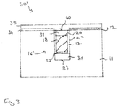
- Figure 1 illustrates a cross-sectional view of a transistor device 10 according to an embodiment.
- the transistor device 10 includes a semiconductor substrate 11 having a main surface 12, a cell field 13 comprising a plurality of transistor cells 14 and an edge termination region 15 which laterally surrounds the cell field 13.
- the plurality of transistor cells 14 in the cell field 13 may all have substantially the same structure.
- the cell field 13 comprises a gate trench 16 in the main surface 12 of the semiconductor substrate 11, a gate dielectric 17 lining the gate trench 16 and a metal gate electrode 18 arranged in the gate trench and on the gate dielectric 17.
- An electrically insulating cap 19 is arranged on the metal gate electrode 18 and is arranged within the gate trench 16.
- Each of the transistor cells 14 in the cell fields may include the same arrangement of the gate trench 16, gate dielectric 17, metal gate electrode 18 and electrically insulating cap 19.
- the cell field 13 contributes to the switching of the transistor device 10, whereas the edge termination region 15 serves to provide electrical isolation between the active device region, i.e. the cell field 13, and the edge region of the device.
- the gate dielectric 17 may be formed by depositing a dielectric layer onto the side walls 22 and base 23 of the gate trench 16.
- a TEOS method may be used, for example.
- the thickness of the gate dielectric 17 may be more uniform if a deposition process rather than a thermal oxidation process of the semiconductor material forming the base 23 and side walls 22 of the gate trench 16 is used.
- the metal gate electrode 18 may comprise a metal such as tungsten for example.
- the metal gate electrode 18 includes two or more sublayers.
- the metal gate electrode 18 includes one or more liner layers which are positioned on and line the gate dielectric 17 and a filler material which is positioned on the liner material and which fills the remainder of the trench, i.e. the gap surrounded by the liner layer(s), to form the metal gate electrode 18.
- the liner layer may be TiN and the filler material tungsten.
- the metal gate electrode 18 includes an upper surface 20 which is positioned within the gate trench 16 and, therefore, at a depth from the main surface 12 within the semiconductor substrate 11.
- the electrically insulating layer 19 extends between and is bounded at its lateral sides by the gate dielectric 17 lining the side walls 22 of the gate trench 16.
- the electrically insulating cap 19 has an upper surface 21 that is substantially coplanar with the main or major surface 12 of the semiconductor substrate 11.
- the electrically insulating cap 19 may be positioned directly on and entirely cover the upper surface 20 of the metal gate electrode 18 at regions of the transistor device 10 positioned within the cell field 13.
- the electrically insulating cap 19 serves to electrically insulate the metal gate electrode 18 from conductive layers positioned above the gate trench 16 in the cell field 13 and from subsequent process steps, for example during fabrication and implantation of the body and source regions of the transistor device and subsequent wet chemical cleaning and/or etching processes.
- the use of the electrically insulating cap 19 also results in a planar surface on which a metallization structure with its interlayer dielectrics can be built up.
- the interlayer dielectric layers commonly formed from undoped silicon glass (USG) and/or BPSG (borophosphosilicate glass), are however, not in direct contact with the metal gate electrode 18 in the cell field 13 due to the presence of the intervening electrically insulating cap 19 positioned in the gate trench 16 on top of the metal gate electrode 18.
- An electrical contact may be made to the metal gate electrode 18 using one or more conductive vias which extend through the electrically insulating cap 19.
- the one or more conductive vias are, however, positioned laterally outside of the cell field 13 and in the edge termination region 15.
- the electrically insulating cap 19 may have a lateral extent such that it does not extend into at least the region of the edge termination region 15 in which the conductive via is placed.
- the metal gate electrode 18 is completely encapsulated by the dielectric material of the gate dielectric 17 and electrically insulating cap 19. At least one opening (not seen in figure 1 ) in the electrically insulating cap 19 is formed to allow a contact to the metal gate electrode 18 to be formed. The opening may be positioned in the edge termination region 15.
- the semiconductor substrate 11 may be formed of a monocrystalline semiconductor substrate such as a monocrystalline silicon wafer.
- the semiconductor substrate may be formed by epitaxial semiconductor layer, for example an epitaxial silicon layer.
- the gate trench 16 may have an elongate stripe-like structure with its length extending into the plane of the drawing.
- the gate trenches 16 of the plurality of transistor cells 14 may extend substantially parallel to one another.
- the gate trench forms part of a grid structure including sections extending in different lateral directions and intersecting one another.
- a grid of longitudinal and transverse trenches may be provided. This arrangement may be used for transistor devices including columnar field plates positioned in columnar field plate trenches, with one columnar trench being laterally surrounded by two longitudinal and two transverse sections providing a continuous, typically square, ring.
- the gate trenches 16 with the gate dielectric 17, the metal gate electrode 18 and electrically insulating cap 19 may be fabricated before the body and source regions of the transistor device are implanted and after any field plate trenches are formed in the major surface 12.
- the transistor device 10 may be a vertical transistor device with a drain region (not shown in figure 1 ) positioned on a second main surface 24 which opposes the main surface 12.
- the semiconductor substrate 11 may form the drift region of the transistor device 10 and be doped with the first conductivity type, e.g. n-type.
- the drain region may be highly doped with a first conductivity type, for example n-type.
- a body region (not shown in figure 1 ) is positioned on the drift region and the comprises dopants of a second conductivity type, e.g. p-type, which opposes first conductivity type.
- a source region(not shown in figure 1 ) is positioned on or in the body region and comprises dopants of a first conductivity type.
- a metallic layer may be positioned on the drain region to form a drain contact for the transistor device 10 on the rear surface.
- a conductive layer may be positioned on the main surface 12 of the semiconductor substrate 11 on the cell field 13 which is electrically coupled to the source region and the field plates, if present, which forms a source contact for the transistor device 10.
- the metal gate electrodes 18 may be coupled to a gate contact for the transistor device 10 which is positioned on the main surface 12 laterally adjacent source contact.
- Figure 2A illustrates a top view of a transistor device 30 and figure 2B a cross-sectional view of the transistor device 30 including a gate trench 16 according to an embodiment.
- the transistor device 30 includes a semiconductor substrate 11 having a main surface 12, a cell field 13 comprising a plurality of transistor cells 14 and an edge termination region 15 laterally surrounding the cell field 13 on all sides.
- the cell field 13 comprises the gate trench 16 in the main surface 12 of the semiconductor substrate 11, a gate dielectric 17 lining the gate trench 16, a metal gate electrode 18 arranged in the gate trench 16 on the gate dielectric 17 and an electrically insulating cap 19 arranged on the metal dielectric 18 and positioned within the gate trench 16.
- the transistor device 30 the gate trench 16 has the form of a grid comprising longitudinal sections 16a extending in the y direction substantially parallel to one another and transverse sections 16b extending in the x direction and extending substantially parallel to one another.
- the gate trenches 16 extend to a gate runner 31 positioned on the main surface 11 laterally adjacent the cell field 13.
- the gate runner 31 extends between the gate trenches 16a, 16b and substantially perpendicularly to the length of the gate trenches 16.
- the gate electrodes 18 positioned within the gate trench 16 also have an elongate shape and are each electrically connected to the gate runner 31.
- the transistor device 30 further comprises a charge compensation structure.
- the charge compensation structure comprises a field plate 33 positioned in a field plate trench 32 that extends into the main surface 12 of the semiconductor substrate 11 and which is positioned laterally adjacent the gate trench 16.
- the field plate 32 is electrically conductive and may be formed of polysilicon, for example.
- the field plate 32 may be electrically isolated from the semiconductor substrate 11 with the field plate trench 33 being lined with an electrically insulating layer which is commonly known as a field oxide.
- the field oxide typically has a larger thickness than the gate dielectric 17.
- the charge compensation structure comprises a columnar field plate 33 positioned in a columnar field trench 32.
- the cell field 13 includes a plurality of field plate trenches 32 that are arranged in a regular array and extend into the semiconductor substrate 11 from the main surface 12.
- Each field plate trench 32 includes a columnar or needle-shaped field plate 33 that is electrically insulated from the semiconductor substrate 11 by an electrically insulating layer 38, or field plate oxide, which lines the base and side walls of the field plate trench 32.
- Each transistor cell can be considered to include a portion of the gate trench 16 and one columnar field plate trench 32.
- Each columnar field plate 32 is positioned at the centre of a region of the main surface 12 that is bounded by two longitudinal trench sections 16a and two transverse trench sections 16b that form a square of the gate trench grid structure.
- the transistor device 30 further includes a first electrically insulating layer 34 which is arranged on the main surface 12 the semiconductor substrate 11 and laterally adjacent the gate trench 16, leaving the gate trench 16 and gate electrode 18 uncovered.
- the first electrically insulating layer 34 may serve as a scattering oxide for the subsequent body and source implants.
- the gate trench 16 includes an electrically insulating cap 19 that is arranged on the metal gate electrode 18 and positioned within the gate trench 16.
- the electrically insulating cap 19 comprises an upper dielectric layer 39 which is positioned in the gate trench 16 on top of the gate electrode 18.
- the upper dielectric layer 39 may have an upper surface 40 which is substantially coplanar with the upper surface 12 of the semiconductor substrate 11.
- the upper surface 20 of the gate electrode 18 is recessed within the trench 16 so that it is positioned at a distance from the main surface 12. This recess at the top of the gate trench 16 is filled with the upper dielectric layer 39.
- a second insulating layer 35 extends continuously over the first insulating layer 34, which is positioned on the main surface 12 of the semiconductor substrate 11 laterally adjacent the gate trench 16, and over the upper dielectric layer 39 arranged in the gate trench 16.
- the electrically insulating cap 19 be considered to include two layers; the upper dielectric layer 39 which is positioned within the gate trench 16 and which is in direct contact with the metal gate electrode 18 and the second insulating layer 35 which is positioned on the upper dielectric layer 39.
- the side walls and base of the gate trench 16 are covered with an insulating layer in the form of the gate dielectric 17 which is typically thinner than the upper dielectric layer 39.
- the transistor device 30 is vertical transistor device, in this embodiment a MOSFET device, with a drain region 41 that is highly doped with the first conductivity type at a second main surface 24 which opposes the main surface 12.
- the semiconductor substrate 11 may form the drift region 42 of the transistor device 30 and is lightly doped with the first conductivity type, e.g. n-type.
- a body region 43 is positioned on the drift region 42 and the comprises dopants of a second conductivity type, e.g. p-type, which opposes first conductivity type.
- a source region 44 is positioned on or in the body region 43 and comprises dopants of a first conductivity type.
- a metallic layer 45 is positioned on the drain region 41 to form a drain contact for the transistor device 30 on the rear surface.
- a conductive layer 46 is positioned on the main surface 12 of the semiconductor substrate 11 on the cell field 13. The conductive layer 46 is electrically coupled to the source region 44 and the field plates 33 and forms a source contact for the transistor device 30.
- One or more insulating layers 47 are positioned between the conductive layer 46 and the second dielectric layer 35. The metal gate electrodes 18 may be coupled to a gate contact for the transistor device 30.
- columnar field plate trenches 32 and columnar field plates 33 are illustrated in plan view as circular, the columnar field plate trenches 32 and field plates 33 are not limited to this shape may have other shapes, for example hexagonal or square.
- the field plate 33 and the field plate 32 trench are elongate and have a stripe-like shape and the gate trench has an elongate stripe-like shape.
- the length of the field plate trench 32 and field plate 33 extends substantially parallel to the length of the elongate gate trench 16 and the elongate metal gate electrode 18.
- the electrically insulating cap 19 may have other structures.
- the electrically insulating cap 19 is formed from a portion of the second insulating layer 35 that extends over the first insulating layer 34 and over the metal gate electrode 18 positioned within the gate trench 16.
- the gate electrode 18 is recessed within the gate trench 16 so that its upper surface 20 is spaced at a distance from the main surface 12 and is positioned within the gate trench 16.
- the second insulating layer 35 extends into the upper portion of the gate trench 16 and is in direct contact with an upper surface 20 of the metal gate electrode 18 that is positioned within the gate trench 16.
- the electrically insulating cap 19 is formed by a portion of the second electrically insulating layer 35 only.
- the side walls and base of the gate trench 16 are covered with an insulating layer in the form of the gate dielectric 17.
- the gate dielectric 17 and the portion of the electrically insulating layer 35 forming the cap 19 form an encapsulation for the metal gate electrode.
- the transistor device 30' includes a gate trench 16' in which the gate dielectric 17 further includes a lower dielectric layer 36 which is positioned at the base 23 of the gate trench 16.
- the gate dielectric 17 lines the sidewalls 22 of the gate trench 16 and may also be positioned on an upper surface 37 of the lower dielectric layer 36.
- the gate dielectric 17 therefore has a greater width at the base 23 of the trench than at the sidewalls 22 of the trench 16.
- the electrically insulating cap 19 comprises an upper dielectric layer 39 having an upper surface 40 which is substantially coplanar with the upper surface 12 of the semiconductor substrate 11.
- the transistor device 30 may include a first insulating layer 34 which is formed on the main surface 12 of the semiconductor substrate 11 laterally adjacent to the gate trench 16 and which leaves the upper dielectric layer 39 uncovered and a second dielectric layer 35 which is positioned on the first electrically insulating layer 34 and which extends over the main surface 12 of the substrate 11 and over the upper dielectric layer 39 positioned within the gate trench 16.
- the electrically insulating cap 19 be considered to include two layers; the upper dielectric layer 39 which is positioned within the gate trench 16 and the second insulating layer 35 which is positioned on the upper dielectric layer 39.
- the gate dielectric layer 17 which lines the sidewalls 22 and either the base 23 of the trench 16 or the upper surface 37 of an additional lower dielectric layer 36 is a deposited layer rather than being formed by thermal oxidation of the material of the semiconductor substrate. In some embodiments, the gate dielectric 17 is a deposited silicon oxide layer.
- a gate dielectric 17 which is formed by deposition can be distinguished from a gate dielectric 17 that is formed by thermal oxidation by an increased uniformity in the thickness of the gate dielectric on the side walls of the trench.
- the gate dielectric 17 may be formed using a TEOS deposition process.
- a further densification of the deposited gate dielectric is carried out, for example by use of a subsequent annealing step.
- a combination of a metal gate electrode 18 and a deposited gate dielectric 17 is found to enable fast switching and results in lower losses which are thought to be the result of a reduction in the gate charge and gate resistance.
- the lower dielectric layer 36 may be deposited using a high density plasma (HDP) process.
- HDP high density plasma
- the upper dielectric layer 39 may comprise a TEOS deposited layer.
- the liner layer of the metal gate electrode 18 is a deposited layer.
- the liner layer may comprise titanium, Ti, and/or titanium nitride, TiN, and the filler material may comprise of tungsten, W.
- the gate dielectric is a TEOS layer
- the liner layer is formed of titanium nitride, TiN
- the filler material is formed of tungsten, W.
- figure 4 which includes figures 4A to 4G .
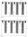
- the process sequence for the gate module is described and illustrated for a silicon power MOSFET using charge-compensation by field-plates in columnar field plate trenches, which are illustrated as separate circular needle trenches.
- this sequence is not limited to needle trenches, for example stripe-like field plate trenches could be used.
- the process is compatible with very high aspect ratios of the trenches, i.e. 3 and higher.
- the aspect ratio is defined as depth/width.
- the aspect ratio is even higher, in our case up to 10, however the techniques described herein could be used for even higher aspect ratios.
- the starting point is a semiconductor substrate 50 having a main surface 51 into which deep field plate trenches 64 with the field-plates 65 have already been produced.
- the semiconductor substrate 50 may be formed of monocrystalline silicon or an epitaxial silicon layer, for example.
- the columnar field plate trenches are illustrated as being circular in plan view.
- the columnar field plate trenches may however have other forms in plan view, for example, square or hexagonal.
- the later position of the gate trench is indicated in figure 4B with dotted lines.
- the gate trench is formed in an area of the main surface 51 positioned between two rows of field plate trenches.
- a gate trench 52 is formed in the main surface 51 which includes a base 53 and sidewalls 54 which extend substantially perpendicularly to the main surface 51.
- the gate trench 52 may have an elongate strip like structure with its length extending into the plane of the drawing.
- a gate dielectric 55 is formed on the main surface 51 of the semiconductor substrate 50 and on the sidewalls 54 and base 53 of the trench 52.
- the gate dielectric 55 may be a silicon oxide layer which may be formed by deposition of a silicon oxide layer on the main surface 51 of the semiconductor substrate 50 as well as on the base 53 and sidewalls 54 of the gate trench 52.
- the gate dielectric 55 may be deposited using a TEOS process and be subsequently subjected to a densification process, for example annealing process.
- a metal gate electrode 59 is then formed on the gate dielectric 55.
- the metal gate electrode 59 is formed by forming one or more liner layers 56 on the gate dielectric 55 and by forming a filler material 57 on the liner layer 56.
- the liner layer 56 may include titanium, for example titanium nitride, and some embodiments may include two or more sublayers, for example titanium and titanium nitride.
- the filler material 57 may be formed of tungsten and may entirely fill the gap in the gate trench 52 which is lined by the liner layer 56 and the gate dielectric 55. The liner layer 56 and the filler material 57 also extends over the major surface 51 of the semiconductor substrate 50 laterally adjacent to the gate trench 52.
- the liner layer 56 may be formed by pulsed chemical vapour deposition (pCVD) or atomic layer deposition (ALD).
- the filler material 57 may be formed by a process enabling conformal deposition, for example metal organic chemical vapour deposition (MOCVD) and may be subjected to a subsequent annealing process.
- pCVD pulsed chemical vapour deposition
- ALD atomic layer deposition
- MOCVD metal organic chemical vapour deposition
- a planarization process may be carried out to produce a planarized surface 58 formed by the gate dielectric layer 55 positioned on the main surface 51 of the semiconductor substrate 50 and the filler material 57 positioned in the gate trench 52.
- the portion of the liner layer 56 arranged on the major surface 51 adjacent to the gate trench 52 is removed.
- a portion of the filler material 57 and liner layer 56 are removed from the upper portion of the gate trench 52 such that the metal gate electrode 59 has an upper surface 60 which is recessed within the trench 52 and is positioned at a distance from the main surface 51 of the substrate 50.
- upper surface 60 of the metal gate electrode 59 may be approximately coplanar with the main surface 51 or recessed within the gate trench 52 by a small distance.
- a first electrically insulating layer 61 is formed on the main surface 51 of the semiconductor substrate 50.
- the first electrically insulating layer 61 may be selectively formed on the semiconductor substrate 50.
- the first electrically insulating layer may extend onto the gate dielectric 55 lining the gate trench 52.
- the metal gate electrode 59 remains uncovered by the first electrically insulating layer 61.
- the first electrically insulating layer 61 may serve as a scattering layer during the subsequent implant of the body region and source region.
- a second insulating layer 62 is then formed which extends over the first electrically insulating layer 61 and over the upper surface 60 of the metal gate electrode 59.
- the portion of the second insulating layer 62 which is positioned directly on the metal gate electrode 59 forms an electrically insulating cap 63 for the metal gate electrode 59.
- the metal gate electrode 59 is completely encapsulated by the dielectric material of the gate dielectric 55 and electrically insulating cap 63.
- the metal gate electrode 59 is completely encapsulated by the dielectric material of the gate dielectric and the electrically insulating cap 63 at all regions of the transistor device.
- at least one opening in the encapsulation is formed to allow a contact to the metal gate electrode to be formed.
- the opening may be positioned in the edge termination region.
- Figure 5 which includes figures 5A to 5I illustrates a method of fabricating a gate of a transistor device according to an embodiment.
- a semiconductor substrate 50 having a main surface 51 and gate trench 52 formed in the main surface 51 is provided.
- the gate trench 52 includes a base 53 and sidewalls 54 which extend substantially perpendicularly to the main surface 51.
- the gate trench 52 has an elongate form having a length extending into the plane of the drawing.
- the semiconductor substrate 50 may also include a charge compensation structure including field plates 65 positioned in field plate trenches 64 which are not seen in the portions of the semiconductor substrate shown in figure 5 .
- the field plates 65 and field plate trenches 64 may be elongate or columnar.
- a lower dielectric layer 70 is formed on the base 53 of the gate trench 52.
- This dielectric layer 70 also has portions 70' which are formed on the main surface 51 of the substrate 50 laterally adjacent the trench 52.
- the lower dielectric layer 70 and the portions 70' may be deposited with a greater thickness on the lateral or horizontal surfaces than on the vertical surfaces such as the side walls 54 of the gate trench 52 using HDP, for example.
- the portions deposited on the vertical surfaces may be removed, for example by use of a wet or dry chemical etching process.
- a gate dielectric layer 55 is then formed which extends over the dielectric layer 70', the sidewalls 54 of the trench 52 and the lower dielectric layer 70 arranged at the base 53 of the gate trench 52.
- the gate dielectric layer 55 may be deposited, for example using TEOS.
- a thicker gate dielectric is provided at the base 53 of the gate trench 52 by a combination of the lower dielectric layer 70 and the deposited gate dielectric layer 55. This increased thickness at the base 53 of the gate trench 52 may be used to further reduce the gate charge and gate drain charge.
- a metal gate electrode 59 is then formed in the gate trench 52 by forming a liner layer 56 on the gate dielectric layer 55 and over the main surface 51 of the semiconductor substrate 50, the sidewalls 54 and base 53 of the trench 52.
- Filler material 57 is then deposited which fills the gap formed in the gate trench 52 by the liner layer 56 and the gate dielectric 55.
- the filler material 57 is also positioned on the major surface 51 of the semiconductor substrate 50 in regions laterally adjacent to the gate trench 52.
- the filler material 57 may be deposited conformally and have a thickness such that any indentation above the gate trench 52 that is caused by conformal deposition of the filler material 57 is positioned above the plane of the liner layer 56 arranged on the main surface 51.
- the liner layer 56 may be formed by pulsed chemical vapour deposition (pCVD) or atomic layer deposition (ALD).
- the filler material 57 may be formed by a process enabling conformal deposition, for example metal organic chemical vapour deposition (MOCVD) and may be subjected to a subsequent annealing process.
- pCVD pulsed chemical vapour deposition
- ALD atomic layer deposition
- MOCVD metal organic chemical vapour deposition
- a planarization process is carried out to remove the filler material 57 and liner layer 56 positioned on the main surface 51 and laterally adjacent the gate trench 52 to provide to form a planarized surface 58 comprising the regions of the dielectric layer 55 positioned on the dielectric layer 70' and the filler material 57.
- the filler material 57 and liner layer 56 are then removed from the gate trench 52 such that a metal gate electrode 59 is formed having an upper surface 60 positioned at a depth from the main surface 51 of the semiconductor substrate 50 and within the gate trench 52, as can be seen in Figure 5F .
- the metallic material of the gate electrode 59 is selectively removed such that the gate dielectric layer 55 remains positioned on the dielectric layer 70' and side walls 54 of the gate trench 52.
- the depth of the upper surface 60 of the gate electrode 59 from the main surface is larger than in the embodiment described with reference to Figure 4 .
- a further electrically insulating layer 71 is formed which fills the upper portion of the gate trench 52 and which extends over the gate dielectric 55 positioned adjacent the gate trench 52.
- the further electrically insulating layer 71 may be deposited using TEOS or a plasma based technique, such as HDP.
- a further planarization process is carried out to remove the dielectric material 71, the gate dielectric 55 and the dielectric material 70' and form a planarized surface 72 which is formed from the material of the semiconductor substrate 50 and the remainder of the electrically insulating layer 71 that is positioned in the upper portion of the gate trench 52 above the metal gate electrode 59.
- the remainder of the electrically insulating layer 71 forms an upper dielectric layer 73 positioned on the upper surface 60 of the gate electrode 59 and within the gate trench 52.
- the upper dielectric layer 73 extends laterally within the gate trench 52 between the gate dielectric 55 positioned on the side walls 54.
- the first electrically insulating layer 61 is then formed on the main surface 51 of the semiconductor substrate 50.
- the first electrically insulating layer 61 may be selectively formed on the main surface 51 by selective oxidation of the semiconductor material of the substrate 50.
- the first electrically insulating layer 61 also extends over the gate dielectric layer 55 lining the gate trench 52 but leaves the upper dielectric layer 73 uncovered.
- the second electrically insulating layer 62 is then formed on the first electrically insulating layer 61 and on the upper dielectric layer 73 in the gate trench 52 as a single continuous layer.
- the second electrically insulating layer 62 may be formed by a TEOS process.
- the first electrically insulating layer 61 is omitted and only the second electrically insulating layer 62 is applied.
- the metallic gate electrode 59 is therefore electrically insulated on its top surface by a combination of the upper dielectric layer 73 and the second insulating layer 62 forming an electrically insulating cap 74, on its bottom surface by the lower dielectric layer 70 and gate dielectric 55 and its side faces by the gate dielectric 55 positioned on the sidewalls 54 of the gate trench 52.
- the electrically insulating cap 74 also results in a planar surface 72 on which the subsequent metallization structure with its interlayer dielectrics can be built up.
- the interlayer dielectric layers commonly formed from undoped silicon glass (USG) and/or BPSG (borophosphosilicate glass), are however, not in direct contact with the metal gate electrode 59 in the gate trench 52 positioned in the cell field due to the presence of the intervening electrically insulating cap 74 positioned in the gate trench 52 on top of the metal gate electrode 59.
- Figure 6A and 6B illustrate cross-sectional views of a transistor device which may include a gate structure according to any one of the embodiments described herein.
- Figures 6A and 6B illustrate a charge compensation structure in the form of a field plate trench 80 which includes a field plate 81 which is electrically insulated from the semiconductor substrate 52 by an electrically insulating layer 82.
- the electrically insulating layer 82 is commonly known as field plate oxide and lines the sidewalls 83 and base 84 of the field plate trench 80.
- the field plate trench 80 may have an elongate strip like structure having a length which extends substantially parallel to the length of the gate trenches 52.
- the field plate trench 80 may have a columnar form and a plurality of field plate trenches columnar field plate trenches are provided which are arranged in a regular array of rows and columns.
- An elongate gate trench may be positioned between two rows of columnar field plate trenches.
- the gate trench 52 includes a lower dielectric layer 70 positioned at its base 53, a gate dielectric 55 positioned on the lower dielectric layer 70 and sidewalls 54 of the gate trench 52.
- the metal gate electrode 59 positioned within the trench is electrically isolated at its top side by the second dielectric layer 62 which extends over the main surface 51 of the semiconductor substrate 50 and into the gate trench 52 where it is in direct contact with the upper surface 60 of the metal gate electrode 59.
- the metal gate electrode 59 is encapsulated by the lower dielectric layer 70 and gate dielectric 55 on its lower side, by the gate dielectric 55 on its side faces and by the second dielectric layer 62 at its upper side.
- the gate trench 52 may have an arrangement in which the metal gate electrode 59 is encapsulated by only the gate dielectric 55 on its lower side and on its side faces and by only the second dielectric layer 62 at its upper side.
- the metal gate electrode 59 is encapsulated by the lower dielectric layer 70 and the gate dielectric 55 on its lower side, by the gate dielectric 55 on its side faces and at its upper side by an additional upper dielectric layer positioned within the gate trench 52 and the second dielectric layer 62 positioned on the additional upper dielectric layer.
- the first dielectric layer 61 is also provided which also extends over main surface 51 of the semiconductor substrate 50 such that the second dielectric layer 62 is positioned on this first dielectric layer 61 in regions laterally adjacent the metal gate electrode 59.
- the field plate trenches and the field plates 81 may be formed in the main surface 51 before fabrication of the gate electrode 55.
- the electrically insulating cap which is provided by the second insulating layer 62 positioned on the metal gate electrode 59 and, if present, the additional upper dielectric layer 73, serves to protect the underlying metal gate electrode 59 during subsequent processing.
- implantation of dopants of the second conductivity type into the main surface 51 to form the body region 85 and implantation of dopants of the first conductivity type to form source region 86 on the body region 85 is performed after fabrication of the gate electrode 59 in the gate trench 52.
- a metallisation structure may then be formed on the main surface 51 to provide electrical connection to the source region 86 and field plates 83 at positions within the cell field 13 and a connection to the metal gate electrodes 59 at a position outside of the cell field 13.
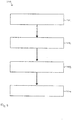
- Figure 7 illustrates a flowchart 100 of fabricating a gate of a transistor device.
- the transistor device comprises a semiconductor substrate having a main surface, a cell field comprising a plurality of transistor cells and an edge termination region laterally surrounding the cell field.
- a gate trench is formed in the main surface of the semiconductor substrate in the cell field.
- the gate trench is lined with a gate dielectric.
- a metal gate electrode is formed on the gate dielectric and within the gate trench.
- an electrically insulating cap is formed on the metal gate electrode and within the gate trench.
- a gate structure is provided in which the metal gate electrode is encapsulated by a gate dielectric on all sides in regions of the metal gate electrode positioned in the active area of the device, i.e. in the cell field.
- the fabrication of a transistor device including a metal gate electrode is simplified as standard wet chemical cleaning techniques can be used in the subsequent process steps during the manufacturing of the device. Therefore, this structure provides a way of overcoming many of the restrictions for the manufacturing of a metal gate device. Furthermore, the top of the gate electrode is not exposed to increased electrical fields, which can lead to an increased lifetime of the device.
Abstract
Description
- Common transistor devices for power applications include Si CoolMOS®, Si Power MOSFETs, and Si Insulated Gate Bipolar Transistors (IGBTs).
US 9,680,004 B2 - Methods allowing simpler manufacturing of transistor devices including a metal gate electrode and transistor devices including a metal gate electrode having even better performance would be desirable.
- According to the invention, a transistor device comprises a semiconductor substrate having a main surface, a cell field comprising a plurality of transistor cells and an edge termination region laterally surrounding the cell field. The cell field comprises a gate trench in the main surface of the semiconductor substrate, a gate dielectric lining the gate trench, a metal gate electrode arranged in the gate trench on the gate dielectric and an electrically insulating cap arranged on the metal gate electrode and within the gate trench.
- In some embodiments, the metal gate electrode has an upper surface that is positioned within the gate trench.
- In some embodiments, the gate dielectric is a deposited layer that has a uniform thickness on the side walls of the trench.
- In some embodiments, the transistor device further comprises a first electrically insulating layer arranged on the main surface of the semiconductor substrate laterally adjacent the gate trench.
- In some embodiments, the first electrically insulating layer extends onto the gate dielectric.
- In some embodiments, the electrically insulating cap forms part of a second electrically insulating layer that extends over the first electrically insulating layer and over the metal gate electrode positioned within the gate trench. The second electrically insulating layer is in direct contact with the upper surface of the metal gate electrode.
- In some embodiments, the gate dielectric further comprises a lower dielectric layer arranged at the base of the gate trench and the gate dielectric lines side walls of the gate trench and is positioned on an upper surface of the lower dielectric layer. In some embodiments, the lower dielectric layer is formed using a HDP (High Density Plasma) deposition process.
- In some embodiments, the electrically insulating cap comprises an upper dielectric layer having an upper surface that is substantially coplanar with the main surface of the semiconductor substrate.
- In some embodiments, the transistor device further comprises a second electrically insulating layer that extends over the main surface of the semiconductor substrate and over the upper dielectric layer positioned in the gate trench. The second electrically insulating layer may comprise a TEOS layer, i.e. is deposited using a TEOS (Tetraethyl orthosilicate) process.
- In some embodiments, the upper dielectric layer comprises a TEOS layer, i.e. is deposited using a TEOS (Tetraethyl orthosilicate) process.
- In some embodiments, the metal gate electrode comprises a liner layer arranged on the gate dielectric and a filler material. The liner layer may include two or more sublayers.
- In some embodiments, the liner layer comprises Ti and/or TiN. In some embodiments, the filler material comprises tungsten. In some embodiments, the liner layer comprises TiN and the filler material is formed of tungsten.
- In some embodiments, the transistor device further comprises a charge compensation structure. The charge compensation structure may comprise one or more electrically conductive field plates or a superjunction structure, for example.
- In some embodiments, the charge compensation structure comprises an elongate field plate in an elongate field plate trench that extends into the main surface and substantially parallel to the gate trench. Each transistor cell may include an elongate field plate so that the charge compensation structure includes a plurality of elongate field plate trenches, each including an elongate field plate.
- In some embodiments, the charge compensation structure comprises a columnar field plate in a columnar field plate trench that extends into the main surface and is positioned laterally adjacent the gate trench. Each transistor cell may include a columnar field plate so that the charge compensation structure includes a plurality of columnar field plate trenches, each including a columnar field plate.
- In some embodiments, the field plate comprises polysilicon. The field plate may be electrically isolated from the semiconductor substrate by an electrically insulating layer or field oxide that lines the base and side walls of the field plate trench. The field oxide may comprise silicon oxide.
- The transistor device may be a MOSFET (Metal Oxide Semiconductor Field Effect Transistor) or a IGBT (Insulated Gate Bipolar Transistor) or a superjunction device.
- A method of fabricating a gate of a transistor device is also provided, the transistor device comprising a semiconductor substrate having a main surface, a cell field comprising a plurality of transistor cells and an edge termination region laterally surrounding the cell field. The method comprises forming a gate trench in the main surface of the semiconductor substrate in the cell field, lining the gate trench with a gate dielectric, forming a metal gate electrode on the gate dielectric and forming an electrically insulating cap on the metal gate electrode and within the gate trench.
- In some embodiments, the gate dielectric is deposited onto a base and side walls of the gate trench.
- In some embodiments, method further comprises removing an upper portion of the metal gate electrode such that an upper surface of the metal gate electrode is recessed within the gate trench.
- In some embodiments, the method further comprises selectively forming an first electrically insulating layer on the main surface of the semiconductor substrate laterally adjacent the gate trench.
- In some embodiments, the method further comprises forming a second electrically insulating layer on the first electrically insulating layer and on the metal gate electrode in the gate trench to form the electrically insulating cap.
- In some embodiments, the method further comprises forming a lower dielectric layer arranged at the base of the gate trench and forming the gate dielectric on the side walls of the gate trench and on an upper surface of the lower dielectric layer.
- In some embodiments, the method further comprises forming an upper dielectric layer on the metal gate electrode to form the electrically insulating cap, the upper dielectric layer having an upper surface that is substantially coplanar with the main surface of the semiconductor substrate, and forming a second electrically insulating layer on the upper dielectric layer and on the main surface of the semiconductor substrate.
- In some embodiments, the method further comprises after the formation of the electrically insulating cap, implanting a body region and a source region into the main surface of the semiconductor substrate.
- Those skilled in the art will recognize additional features and advantages upon reading the following detailed description, and upon viewing the accompanying drawings.
- The elements of the drawings are not necessarily to scale relative to each other. Like reference numerals designate corresponding similar parts. The features of the various illustrated embodiments can be combined unless they exclude each other. Exemplary embodiments are depicted in the drawings and are detailed in the description which follows.
-
Figure 1 illustrates a cross-sectional view of a transistor device including a gate trench according to an embodiment. -
Figure 2A illustrates a top view of a transistor device according to an embodiment. -
Figure 2B illustrates a cross-sectional view of the transistor device offigure 2A . -
Figure 2C illustrates a cross-sectional view of a transistor device according to an embodiment. -
Figure 3 illustrates a cross-sectional view of a transistor device including a gate trench according to an embodiment. -
Figure 4 , which includesfigures 4A to 4I , illustrates a method of fabricating a gate of a transistor device. -
Figure 5 , which includesfigures 5A to 5I , illustrates a method of fabricating a gate of a transistor device according to an embodiment. -
Figure 6 , which includesfigures 6A and 6B , illustrates a method of fabricating a transistor device including the gate trench of one of the embodiments described herein. -
Figure 7 illustrates a flowchart of fabricating a gate of a transistor device. - In the following detailed description, reference is made to the accompanying drawings, which form a part hereof, and in which is shown by way of illustration specific embodiments in which the invention may be practiced. In this regard, directional terminology, such as "top", "bottom", "front", "back", "leading", "trailing", etc., is used with reference to the orientation of the figure(s) being described. Because components of the embodiments can be positioned in a number of different orientations, the directional terminology is used for purposes of illustration and is in no way limiting. It is to be understood that other embodiments may be utilized and structural or logical changes may be made without departing from the scope of the present invention. The following detailed description, thereof, is not to be taken in a limiting sense, and the scope of the present invention is defined by the appended claims.
- A number of exemplary embodiments will be explained below. In this case, identical structural features are identified by identical or similar reference symbols in the figures. In the context of the present description, "lateral" or "lateral direction" should be understood to mean a direction or extent that runs generally parallel to the lateral extent of a semiconductor material or semiconductor carrier. The lateral direction thus extends generally parallel to these surfaces or sides. In contrast thereto, the term "vertical" or "vertical direction" is understood to mean a direction that runs generally perpendicular to these surfaces or sides and thus to the lateral direction. The vertical direction therefore runs in the thickness direction of the semiconductor material or semiconductor carrier.
- As employed in this specification, when an element such as a layer, region or substrate is referred to as being "on" or extending "onto" another element, it can be directly on or extend directly onto the other element or intervening elements may also be present. In contrast, when an element is referred to as being "directly on" or extending "directly onto" another element, there are no intervening elements present.
- As employed in this specification, when an element is referred to as being "connected" or "coupled" to another element, it can be directly connected or coupled to the other element or intervening elements may be present. In contrast, when an element is referred to as being "directly connected" or "directly coupled" to another element, there are no intervening elements present.
- As used herein, various device types and/or doped semiconductor regions may be identified as being of n type or p type, but this is merely for convenience of description and not intended to be limiting, and such identification may be replaced by the more general description of being of a "first conductivity type" or a "second, opposite conductivity type" where the first type may be either n or p type and the second type then is either p or n type.
- The Figures illustrate relative doping concentrations by indicating "-" or "+" next to the doping type "n" or "p". For example, "n-" means a doping concentration which is lower than the doping concentration of an "n"-doping region while an "n+"-doping region has a higher doping concentration than an "n"-doping region. Doping regions of the same relative doping concentration do not necessarily have the same absolute doping concentration. For example, two different "n"-doping regions may have the same or different absolute doping concentrations.
- For modern trench power MOSFETs, the constant shrink of the dimensions in order to gain better area-specific on-resistance results in very small gate dimensions. Commonly, polysilicon which is used as gate material. For small dimensions, the sheet resistance and specific resistivity of polysilicon is relatively high which can lead to an increase of the distributed gate resistance over the chip. This can cause inhomogeneous switching over the chip as well as a slow-down in the switching speed as the gate resistance is increasing. Consequently, the possibilities for further reducing switching losses are limited and device ruggedness can be negatively affected.
- One approach to mitigate these effects is based on the implementation of metal fingers which contact the polysilicon gates of the single transistor cells. However, this requires silicon area which cannot be used for switching.
- Another approach is the use of metal in place of polysilicon as the gate material. The much higher conductivity of metals with respect to doped polysilicon eliminates the need for gate fingers in order to provide a homogeneous switching over the full chip and enables a reduction of the trench width. By using a metal gate, e.g. a TiN/W gate, a reduction of the specific resistivity of the gate compared to a polysilicon gate can be achieved. A metal gate offers a way of enabling lower gate dimensions and thus smaller device dimensions and improving the switching speed, as well as enabling a homogenous switching over the whole chip area. However, it is not straightforward to manufacture a silicon device with a metal gate, as this means integrating metal into the front end of line process.
- Embodiments described herein provide a gate trench structure filled with a metallic gate electrode material, which is encapsulated by an electrically insulating capping layer, for example, an oxide capping layer. In some embodiments, charge-compensation by field plates in field plate trenches or needle-shaped or columnar field plates in needle-shaped or columnar field plate trenches are used.
- Encapsulating the metal gate electrode according to embodiments described herein allows for the use of the standard wet chemical cleaning in the subsequent process steps during the manufacturing of the device. Therefore, this structure provides a way of overcoming many of the restrictions for the manufacturing of a metal gate device. Furthermore, the top of the gate electrode is not exposed to increased electrical fields, which is useful for increasing the lifetime of the device.
-
Figure 1 illustrates a cross-sectional view of atransistor device 10 according to an embodiment. Thetransistor device 10 includes asemiconductor substrate 11 having amain surface 12, acell field 13 comprising a plurality oftransistor cells 14 and anedge termination region 15 which laterally surrounds thecell field 13. The plurality oftransistor cells 14 in thecell field 13 may all have substantially the same structure. - The
cell field 13 comprises agate trench 16 in themain surface 12 of thesemiconductor substrate 11, agate dielectric 17 lining thegate trench 16 and ametal gate electrode 18 arranged in the gate trench and on thegate dielectric 17. An electrically insulatingcap 19 is arranged on themetal gate electrode 18 and is arranged within thegate trench 16. - Each of the
transistor cells 14 in the cell fields may include the same arrangement of thegate trench 16,gate dielectric 17,metal gate electrode 18 and electrically insulatingcap 19. Thecell field 13 contributes to the switching of thetransistor device 10, whereas theedge termination region 15 serves to provide electrical isolation between the active device region, i.e. thecell field 13, and the edge region of the device. - The
gate dielectric 17 may be formed by depositing a dielectric layer onto theside walls 22 andbase 23 of thegate trench 16. A TEOS method may be used, for example. The thickness of thegate dielectric 17 may be more uniform if a deposition process rather than a thermal oxidation process of the semiconductor material forming thebase 23 andside walls 22 of thegate trench 16 is used. - The
metal gate electrode 18 may comprise a metal such as tungsten for example. In some embodiments, themetal gate electrode 18 includes two or more sublayers. In some embodiments, themetal gate electrode 18 includes one or more liner layers which are positioned on and line thegate dielectric 17 and a filler material which is positioned on the liner material and which fills the remainder of the trench, i.e. the gap surrounded by the liner layer(s), to form themetal gate electrode 18. The liner layer may be TiN and the filler material tungsten. - The
metal gate electrode 18 includes anupper surface 20 which is positioned within thegate trench 16 and, therefore, at a depth from themain surface 12 within thesemiconductor substrate 11. The electrically insulatinglayer 19 extends between and is bounded at its lateral sides by thegate dielectric 17 lining theside walls 22 of thegate trench 16.
In some embodiments, the electrically insulatingcap 19 has anupper surface 21 that is substantially coplanar with the main ormajor surface 12 of thesemiconductor substrate 11. The electrically insulatingcap 19 may be positioned directly on and entirely cover theupper surface 20 of themetal gate electrode 18 at regions of thetransistor device 10 positioned within thecell field 13. - The electrically insulating
cap 19 serves to electrically insulate themetal gate electrode 18 from conductive layers positioned above thegate trench 16 in thecell field 13 and from subsequent process steps, for example during fabrication and implantation of the body and source regions of the transistor device and subsequent wet chemical cleaning and/or etching processes. - The use of the electrically insulating
cap 19 also results in a planar surface on which a metallization structure with its interlayer dielectrics can be built up. The interlayer dielectric layers, commonly formed from undoped silicon glass (USG) and/or BPSG (borophosphosilicate glass), are however, not in direct contact with themetal gate electrode 18 in thecell field 13 due to the presence of the intervening electrically insulatingcap 19 positioned in thegate trench 16 on top of themetal gate electrode 18. - An electrical contact may be made to the
metal gate electrode 18 using one or more conductive vias which extend through the electrically insulatingcap 19. The one or more conductive vias are, however, positioned laterally outside of thecell field 13 and in theedge termination region 15. In some embodiments, the electrically insulatingcap 19 may have a lateral extent such that it does not extend into at least the region of theedge termination region 15 in which the conductive via is placed. - At positions within the
cell field 13 of thetransistor device 10, themetal gate electrode 18 is completely encapsulated by the dielectric material of thegate dielectric 17 and electrically insulatingcap 19. At least one opening (not seen infigure 1 ) in the electrically insulatingcap 19 is formed to allow a contact to themetal gate electrode 18 to be formed. The opening may be positioned in theedge termination region 15. - The
semiconductor substrate 11 may be formed of a monocrystalline semiconductor substrate such as a monocrystalline silicon wafer. In some embodiments, the semiconductor substrate may be formed by epitaxial semiconductor layer, for example an epitaxial silicon layer. - The
gate trench 16 may have an elongate stripe-like structure with its length extending into the plane of the drawing. Thegate trenches 16 of the plurality oftransistor cells 14 may extend substantially parallel to one another. - In some embodiments, the gate trench forms part of a grid structure including sections extending in different lateral directions and intersecting one another. For example, a grid of longitudinal and transverse trenches may be provided. This arrangement may be used for transistor devices including columnar field plates positioned in columnar field plate trenches, with one columnar trench being laterally surrounded by two longitudinal and two transverse sections providing a continuous, typically square, ring.
- The
gate trenches 16 with thegate dielectric 17, themetal gate electrode 18 and electrically insulatingcap 19 may be fabricated before the body and source regions of the transistor device are implanted and after any field plate trenches are formed in themajor surface 12. - The
transistor device 10 may be a vertical transistor device with a drain region (not shown infigure 1 ) positioned on a secondmain surface 24 which opposes themain surface 12. Thesemiconductor substrate 11 may form the drift region of thetransistor device 10 and be doped with the first conductivity type, e.g. n-type. The drain region may be highly doped with a first conductivity type, for example n-type. A body region (not shown infigure 1 ) is positioned on the drift region and the comprises dopants of a second conductivity type, e.g. p-type, which opposes first conductivity type. A source region(not shown infigure 1 ) is positioned on or in the body region and comprises dopants of a first conductivity type. - A metallic layer may be positioned on the drain region to form a drain contact for the
transistor device 10 on the rear surface. A conductive layer may be positioned on themain surface 12 of thesemiconductor substrate 11 on thecell field 13 which is electrically coupled to the source region and the field plates, if present, which forms a source contact for thetransistor device 10. Themetal gate electrodes 18 may be coupled to a gate contact for thetransistor device 10 which is positioned on themain surface 12 laterally adjacent source contact. -
Figure 2A illustrates a top view of atransistor device 30 andfigure 2B a cross-sectional view of thetransistor device 30 including agate trench 16 according to an embodiment. - The
transistor device 30 includes asemiconductor substrate 11 having amain surface 12, acell field 13 comprising a plurality oftransistor cells 14 and anedge termination region 15 laterally surrounding thecell field 13 on all sides. Thecell field 13 comprises thegate trench 16 in themain surface 12 of thesemiconductor substrate 11, agate dielectric 17 lining thegate trench 16, ametal gate electrode 18 arranged in thegate trench 16 on thegate dielectric 17 and an electrically insulatingcap 19 arranged on themetal dielectric 18 and positioned within thegate trench 16. - As can be seen in the top view of
figure 2A , thetransistor device 30 thegate trench 16 has the form of a grid comprisinglongitudinal sections 16a extending in the y direction substantially parallel to one another and transverse sections 16b extending in the x direction and extending substantially parallel to one another. - The
gate trenches 16 extend to agate runner 31 positioned on themain surface 11 laterally adjacent thecell field 13. Thegate runner 31 extends between thegate trenches 16a, 16b and substantially perpendicularly to the length of thegate trenches 16. Thegate electrodes 18 positioned within thegate trench 16 also have an elongate shape and are each electrically connected to thegate runner 31. - The
transistor device 30 further comprises a charge compensation structure. In some embodiments, such as that illustrated infigure 2 , the charge compensation structure comprises afield plate 33 positioned in afield plate trench 32 that extends into themain surface 12 of thesemiconductor substrate 11 and which is positioned laterally adjacent thegate trench 16. Thefield plate 32 is electrically conductive and may be formed of polysilicon, for example. Thefield plate 32 may be electrically isolated from thesemiconductor substrate 11 with thefield plate trench 33 being lined with an electrically insulating layer which is commonly known as a field oxide. The field oxide typically has a larger thickness than thegate dielectric 17. - In some embodiments, such as that illustrated in
figure 2 , the charge compensation structure comprises acolumnar field plate 33 positioned in acolumnar field trench 32. Thecell field 13 includes a plurality offield plate trenches 32 that are arranged in a regular array and extend into thesemiconductor substrate 11 from themain surface 12. Eachfield plate trench 32 includes a columnar or needle-shapedfield plate 33 that is electrically insulated from thesemiconductor substrate 11 by an electrically insulatinglayer 38, or field plate oxide, which lines the base and side walls of thefield plate trench 32. Each transistor cell can be considered to include a portion of thegate trench 16 and one columnarfield plate trench 32. - Each
columnar field plate 32 is positioned at the centre of a region of themain surface 12 that is bounded by twolongitudinal trench sections 16a and two transverse trench sections 16b that form a square of the gate trench grid structure. - Referring to the cross-sectional view of
Figure 2B , thetransistor device 30 further includes a first electrically insulatinglayer 34 which is arranged on themain surface 12 thesemiconductor substrate 11 and laterally adjacent thegate trench 16, leaving thegate trench 16 andgate electrode 18 uncovered. The first electrically insulatinglayer 34 may serve as a scattering oxide for the subsequent body and source implants. - The
gate trench 16 includes an electrically insulatingcap 19 that is arranged on themetal gate electrode 18 and positioned within thegate trench 16. In some embodiments, such as that illustrated infigure 2B , the electrically insulatingcap 19 comprises anupper dielectric layer 39 which is positioned in thegate trench 16 on top of thegate electrode 18. Theupper dielectric layer 39 may have anupper surface 40 which is substantially coplanar with theupper surface 12 of thesemiconductor substrate 11. Theupper surface 20 of thegate electrode 18 is recessed within thetrench 16 so that it is positioned at a distance from themain surface 12. This recess at the top of thegate trench 16 is filled with theupper dielectric layer 39. - A second insulating
layer 35 extends continuously over the first insulatinglayer 34, which is positioned on themain surface 12 of thesemiconductor substrate 11 laterally adjacent thegate trench 16, and over theupper dielectric layer 39 arranged in thegate trench 16. - The electrically insulating
cap 19 be considered to include two layers; theupper dielectric layer 39 which is positioned within thegate trench 16 and which is in direct contact with themetal gate electrode 18 and the second insulatinglayer 35 which is positioned on theupper dielectric layer 39. - The side walls and base of the
gate trench 16 are covered with an insulating layer in the form of thegate dielectric 17 which is typically thinner than theupper dielectric layer 39. - The
transistor device 30 is vertical transistor device, in this embodiment a MOSFET device, with adrain region 41 that is highly doped with the first conductivity type at a secondmain surface 24 which opposes themain surface 12. Thesemiconductor substrate 11 may form thedrift region 42 of thetransistor device 30 and is lightly doped with the first conductivity type, e.g. n-type. Abody region 43 is positioned on thedrift region 42 and the comprises dopants of a second conductivity type, e.g. p-type, which opposes first conductivity type. Asource region 44 is positioned on or in thebody region 43 and comprises dopants of a first conductivity type. - A
metallic layer 45 is positioned on thedrain region 41 to form a drain contact for thetransistor device 30 on the rear surface. Aconductive layer 46 is positioned on themain surface 12 of thesemiconductor substrate 11 on thecell field 13. Theconductive layer 46 is electrically coupled to thesource region 44 and thefield plates 33 and forms a source contact for thetransistor device 30. One or moreinsulating layers 47 are positioned between theconductive layer 46 and thesecond dielectric layer 35. Themetal gate electrodes 18 may be coupled to a gate contact for thetransistor device 30. - Whilst the columnar
field plate trenches 32 andcolumnar field plates 33 are illustrated in plan view as circular, the columnarfield plate trenches 32 andfield plates 33 are not limited to this shape may have other shapes, for example hexagonal or square. - In other non-illustrated embodiments, the
field plate 33 and thefield plate 32 trench are elongate and have a stripe-like shape and the gate trench has an elongate stripe-like shape. The length of thefield plate trench 32 andfield plate 33 extends substantially parallel to the length of theelongate gate trench 16 and the elongatemetal gate electrode 18. - The electrically insulating
cap 19 may have other structures. In some embodiments, such as that illustrated inFigure 2C , the electrically insulatingcap 19 is formed from a portion of the second insulatinglayer 35 that extends over the first insulatinglayer 34 and over themetal gate electrode 18 positioned within thegate trench 16. In this embodiment, thegate electrode 18 is recessed within thegate trench 16 so that itsupper surface 20 is spaced at a distance from themain surface 12 and is positioned within thegate trench 16. The second insulatinglayer 35 extends into the upper portion of thegate trench 16 and is in direct contact with anupper surface 20 of themetal gate electrode 18 that is positioned within thegate trench 16. - In the embodiment illustrated in
figure 2C , the electrically insulatingcap 19 is formed by a portion of the second electrically insulatinglayer 35 only. The side walls and base of thegate trench 16 are covered with an insulating layer in the form of thegate dielectric 17. Thegate dielectric 17 and the portion of the electrically insulatinglayer 35 forming thecap 19 form an encapsulation for the metal gate electrode. - Referring to
figure 3 , in some embodiments, the transistor device 30' includes a gate trench 16' in which thegate dielectric 17 further includes a lowerdielectric layer 36 which is positioned at thebase 23 of thegate trench 16. Thegate dielectric 17 lines thesidewalls 22 of thegate trench 16 and may also be positioned on anupper surface 37 of the lowerdielectric layer 36. Thegate dielectric 17 therefore has a greater width at thebase 23 of the trench than at thesidewalls 22 of thetrench 16. - In some embodiments, such as that illustrated in
figure 3 , the electrically insulatingcap 19 comprises anupper dielectric layer 39 having anupper surface 40 which is substantially coplanar with theupper surface 12 of thesemiconductor substrate 11. In this arrangement, thetransistor device 30 may include a first insulatinglayer 34 which is formed on themain surface 12 of thesemiconductor substrate 11 laterally adjacent to thegate trench 16 and which leaves theupper dielectric layer 39 uncovered and asecond dielectric layer 35 which is positioned on the first electrically insulatinglayer 34 and which extends over themain surface 12 of thesubstrate 11 and over theupper dielectric layer 39 positioned within thegate trench 16. - In contrast to the embodiment illustrated in
figure 2C , the electrically insulatingcap 19 be considered to include two layers; theupper dielectric layer 39 which is positioned within thegate trench 16 and the second insulatinglayer 35 which is positioned on theupper dielectric layer 39. - In some embodiments, the
gate dielectric layer 17 which lines thesidewalls 22 and either thebase 23 of thetrench 16 or theupper surface 37 of an additional lowerdielectric layer 36 is a deposited layer rather than being formed by thermal oxidation of the material of the semiconductor substrate. In some embodiments, thegate dielectric 17 is a deposited silicon oxide layer. - A
gate dielectric 17 which is formed by deposition can be distinguished from agate dielectric 17 that is formed by thermal oxidation by an increased uniformity in the thickness of the gate dielectric on the side walls of the trench. Thegate dielectric 17 may be formed using a TEOS deposition process. In some embodiments, a further densification of the deposited gate dielectric is carried out, for example by use of a subsequent annealing step. - A combination of a
metal gate electrode 18 and a depositedgate dielectric 17 is found to enable fast switching and results in lower losses which are thought to be the result of a reduction in the gate charge and gate resistance. - In embodiments including a lower
dielectric layer 36, the lowerdielectric layer 36 may be deposited using a high density plasma (HDP) process. - In embodiments including an
upper dielectric layer 39, theupper dielectric layer 39 may comprise a TEOS deposited layer. - In some embodiments, the liner layer of the
metal gate electrode 18 is a deposited layer. The liner layer may comprise titanium, Ti, and/or titanium nitride, TiN, and the filler material may comprise of tungsten, W. - In an embodiment, the gate dielectric is a TEOS layer, the liner layer is formed of titanium nitride, TiN, and the filler material is formed of tungsten, W.
- The method of fabricating a gate of a transistor device will now be described with reference to
figure 4 , which includesfigures 4A to 4G . - In the following, the process sequence for the gate module is described and illustrated for a silicon power MOSFET using charge-compensation by field-plates in columnar field plate trenches, which are illustrated as separate circular needle trenches. However, this sequence is not limited to needle trenches, for example stripe-like field plate trenches could be used.
- The process is compatible with very high aspect ratios of the trenches, i.e. 3 and higher. The aspect ratio is defined as depth/width. After the gate oxide module, the aspect ratio is even higher, in our case up to 10, however the techniques described herein could be used for even higher aspect ratios.
- Referring to the top view of
figure 4A and the cross-sectional view offigure 4B , the starting point is asemiconductor substrate 50 having amain surface 51 into which deepfield plate trenches 64 with the field-plates 65 have already been produced. However, the body and source region of the transistor structure have not yet been formed. Thesemiconductor substrate 50 may be formed of monocrystalline silicon or an epitaxial silicon layer, for example. The columnar field plate trenches are illustrated as being circular in plan view. The columnar field plate trenches may however have other forms in plan view, for example, square or hexagonal. The later position of the gate trench is indicated infigure 4B with dotted lines. - In
figures 4C to 4I , only the region of thesemiconductor substrate 50 including the gate trench is illustrated. - Referring to
figure 4C , the gate trench is formed in an area of themain surface 51 positioned between two rows of field plate trenches. - A
gate trench 52 is formed in themain surface 51 which includes abase 53 andsidewalls 54 which extend substantially perpendicularly to themain surface 51. Thegate trench 52 may have an elongate strip like structure with its length extending into the plane of the drawing. - Referring to
figure 4D , agate dielectric 55 is formed on themain surface 51 of thesemiconductor substrate 50 and on thesidewalls 54 andbase 53 of thetrench 52. Thegate dielectric 55 may be a silicon oxide layer which may be formed by deposition of a silicon oxide layer on themain surface 51 of thesemiconductor substrate 50 as well as on thebase 53 and sidewalls 54 of thegate trench 52. Thegate dielectric 55 may be deposited using a TEOS process and be subsequently subjected to a densification process, for example annealing process. - Referring to
figures 4E and 4F , ametal gate electrode 59 is then formed on thegate dielectric 55. Themetal gate electrode 59 is formed by forming one or more liner layers 56 on thegate dielectric 55 and by forming afiller material 57 on theliner layer 56. - The
liner layer 56 may include titanium, for example titanium nitride, and some embodiments may include two or more sublayers, for example titanium and titanium nitride. Thefiller material 57 may be formed of tungsten and may entirely fill the gap in thegate trench 52 which is lined by theliner layer 56 and thegate dielectric 55. Theliner layer 56 and thefiller material 57 also extends over themajor surface 51 of thesemiconductor substrate 50 laterally adjacent to thegate trench 52. - The
liner layer 56 may be formed by pulsed chemical vapour deposition (pCVD) or atomic layer deposition (ALD). Thefiller material 57 may be formed by a process enabling conformal deposition, for example metal organic chemical vapour deposition (MOCVD) and may be subjected to a subsequent annealing process. - Referring to
figure 4G , a planarization process may be carried out to produce aplanarized surface 58 formed by thegate dielectric layer 55 positioned on themain surface 51 of thesemiconductor substrate 50 and thefiller material 57 positioned in thegate trench 52. The portion of theliner layer 56 arranged on themajor surface 51 adjacent to thegate trench 52 is removed. - Referring to
figure 4H , a portion of thefiller material 57 andliner layer 56 are removed from the upper portion of thegate trench 52 such that themetal gate electrode 59 has an upper surface 60 which is recessed within thetrench 52 and is positioned at a distance from themain surface 51 of thesubstrate 50. In this embodiment, upper surface 60 of themetal gate electrode 59 may be approximately coplanar with themain surface 51 or recessed within thegate trench 52 by a small distance. - Referring to
figure 4I , a first electrically insulatinglayer 61 is formed on themain surface 51 of thesemiconductor substrate 50. The first electrically insulatinglayer 61 may be selectively formed on thesemiconductor substrate 50. In some embodiments, the first electrically insulating layer may extend onto thegate dielectric 55 lining thegate trench 52. Themetal gate electrode 59 remains uncovered by the first electrically insulatinglayer 61. The first electrically insulatinglayer 61 may serve as a scattering layer during the subsequent implant of the body region and source region. - A second insulating
layer 62 is then formed which extends over the first electrically insulatinglayer 61 and over the upper surface 60 of themetal gate electrode 59. The portion of the second insulatinglayer 62 which is positioned directly on themetal gate electrode 59 forms an electrically insulatingcap 63 for themetal gate electrode 59. At positions within the active region of the transistor device, themetal gate electrode 59 is completely encapsulated by the dielectric material of thegate dielectric 55 and electrically insulatingcap 63. - At this stage in the method, the
metal gate electrode 59 is completely encapsulated by the dielectric material of the gate dielectric and the electrically insulatingcap 63 at all regions of the transistor device. In a later stage, at least one opening in the encapsulation is formed to allow a contact to the metal gate electrode to be formed. The opening may be positioned in the edge termination region. -
Figure 5 , which includesfigures 5A to 5I illustrates a method of fabricating a gate of a transistor device according to an embodiment. - Referring to
figure 5A , asemiconductor substrate 50 having amain surface 51 andgate trench 52 formed in themain surface 51 is provided. Thegate trench 52 includes abase 53 andsidewalls 54 which extend substantially perpendicularly to themain surface 51. Thegate trench 52 has an elongate form having a length extending into the plane of the drawing. As in the embodiments described with reference tofigure 4 , thesemiconductor substrate 50 may also include a charge compensation structure includingfield plates 65 positioned infield plate trenches 64 which are not seen in the portions of the semiconductor substrate shown infigure 5 . Thefield plates 65 andfield plate trenches 64 may be elongate or columnar. - Referring to
figure 5B , a lowerdielectric layer 70 is formed on thebase 53 of thegate trench 52. Thisdielectric layer 70 also has portions 70' which are formed on themain surface 51 of thesubstrate 50 laterally adjacent thetrench 52. The lowerdielectric layer 70 and the portions 70' may be deposited with a greater thickness on the lateral or horizontal surfaces than on the vertical surfaces such as theside walls 54 of thegate trench 52 using HDP, for example. In a subsequent process, the portions deposited on the vertical surfaces may be removed, for example by use of a wet or dry chemical etching process. - Referring to
figure 5C , agate dielectric layer 55 is then formed which extends over the dielectric layer 70', thesidewalls 54 of thetrench 52 and the lowerdielectric layer 70 arranged at thebase 53 of thegate trench 52. Thegate dielectric layer 55 may be deposited, for example using TEOS. In this embodiment, a thicker gate dielectric is provided at thebase 53 of thegate trench 52 by a combination of the lowerdielectric layer 70 and the depositedgate dielectric layer 55. This increased thickness at thebase 53 of thegate trench 52 may be used to further reduce the gate charge and gate drain charge. - Referring to
figure 5D , ametal gate electrode 59 is then formed in thegate trench 52 by forming aliner layer 56 on thegate dielectric layer 55 and over themain surface 51 of thesemiconductor substrate 50, thesidewalls 54 andbase 53 of thetrench 52.Filler material 57 is then deposited which fills the gap formed in thegate trench 52 by theliner layer 56 and thegate dielectric 55. Thefiller material 57 is also positioned on themajor surface 51 of thesemiconductor substrate 50 in regions laterally adjacent to thegate trench 52. Thefiller material 57 may be deposited conformally and have a thickness such that any indentation above thegate trench 52 that is caused by conformal deposition of thefiller material 57 is positioned above the plane of theliner layer 56 arranged on themain surface 51. - The
liner layer 56 may be formed by pulsed chemical vapour deposition (pCVD) or atomic layer deposition (ALD). Thefiller material 57 may be formed by a process enabling conformal deposition, for example metal organic chemical vapour deposition (MOCVD) and may be subjected to a subsequent annealing process. - Referring to
figure 5E , a planarization process is carried out to remove thefiller material 57 andliner layer 56 positioned on themain surface 51 and laterally adjacent thegate trench 52 to provide to form aplanarized surface 58 comprising the regions of thedielectric layer 55 positioned on the dielectric layer 70' and thefiller material 57. - The
filler material 57 andliner layer 56 are then removed from thegate trench 52 such that ametal gate electrode 59 is formed having an upper surface 60 positioned at a depth from themain surface 51 of thesemiconductor substrate 50 and within thegate trench 52, as can be seen inFigure 5F . The metallic material of thegate electrode 59 is selectively removed such that thegate dielectric layer 55 remains positioned on the dielectric layer 70' andside walls 54 of thegate trench 52. The depth of the upper surface 60 of thegate electrode 59 from the main surface is larger than in the embodiment described with reference toFigure 4 . - Referring to
Figure 5F , in this embodiment, a further electrically insulatinglayer 71 is formed which fills the upper portion of thegate trench 52 and which extends over thegate dielectric 55 positioned adjacent thegate trench 52. The further electrically insulatinglayer 71 may be deposited using TEOS or a plasma based technique, such as HDP. - Referring to
Figure 5G , a further planarization process is carried out to remove thedielectric material 71, thegate dielectric 55 and the dielectric material 70' and form a planarized surface 72 which is formed from the material of thesemiconductor substrate 50 and the remainder of the electrically insulatinglayer 71 that is positioned in the upper portion of thegate trench 52 above themetal gate electrode 59. The remainder of the electrically insulatinglayer 71 forms anupper dielectric layer 73 positioned on the upper surface 60 of thegate electrode 59 and within thegate trench 52. Theupper dielectric layer 73 extends laterally within thegate trench 52 between thegate dielectric 55 positioned on theside walls 54. - Referring to
figure 5H , the first electrically insulatinglayer 61 is then formed on themain surface 51 of thesemiconductor substrate 50. The first electrically insulatinglayer 61 may be selectively formed on themain surface 51 by selective oxidation of the semiconductor material of thesubstrate 50. In some embodiments, the first electrically insulatinglayer 61 also extends over thegate dielectric layer 55 lining thegate trench 52 but leaves theupper dielectric layer 73 uncovered. The second electrically insulatinglayer 62 is then formed on the first electrically insulatinglayer 61 and on theupper dielectric layer 73 in thegate trench 52 as a single continuous layer. The second electrically insulatinglayer 62 may be formed by a TEOS process. In some embodiments, the first electrically insulatinglayer 61 is omitted and only the second electrically insulatinglayer 62 is applied. - The
metallic gate electrode 59 is therefore electrically insulated on its top surface by a combination of theupper dielectric layer 73 and the second insulatinglayer 62 forming an electrically insulating cap 74, on its bottom surface by the lowerdielectric layer 70 andgate dielectric 55 and its side faces by thegate dielectric 55 positioned on thesidewalls 54 of thegate trench 52. - The electrically insulating cap 74 also results in a planar surface 72 on which the subsequent metallization structure with its interlayer dielectrics can be built up. The interlayer dielectric layers, commonly formed from undoped silicon glass (USG) and/or BPSG (borophosphosilicate glass), are however, not in direct contact with the
metal gate electrode 59 in thegate trench 52 positioned in the cell field due to the presence of the intervening electrically insulating cap 74 positioned in thegate trench 52 on top of themetal gate electrode 59. -
Figure 6A and 6B illustrate cross-sectional views of a transistor device which may include a gate structure according to any one of the embodiments described herein.Figures 6A and 6B illustrate a charge compensation structure in the form of afield plate trench 80 which includes a field plate 81 which is electrically insulated from thesemiconductor substrate 52 by an electrically insulating layer 82. The electrically insulating layer 82 is commonly known as field plate oxide and lines thesidewalls 83 andbase 84 of thefield plate trench 80. In some embodiments, thefield plate trench 80 may have an elongate strip like structure having a length which extends substantially parallel to the length of thegate trenches 52. In other embodiments, thefield plate trench 80 may have a columnar form and a plurality of field plate trenches columnar field plate trenches are provided which are arranged in a regular array of rows and columns. An elongate gate trench may be positioned between two rows of columnar field plate trenches. - In the embodiment illustrated in
figure 6A , thegate trench 52 includes a lowerdielectric layer 70 positioned at itsbase 53, agate dielectric 55 positioned on the lowerdielectric layer 70 and sidewalls 54 of thegate trench 52. Themetal gate electrode 59 positioned within the trench is electrically isolated at its top side by thesecond dielectric layer 62 which extends over themain surface 51 of thesemiconductor substrate 50 and into thegate trench 52 where it is in direct contact with the upper surface 60 of themetal gate electrode 59. - In the embodiment illustrated in
Figure 6 , themetal gate electrode 59 is encapsulated by the lowerdielectric layer 70 andgate dielectric 55 on its lower side, by thegate dielectric 55 on its side faces and by thesecond dielectric layer 62 at its upper side. - In other embodiments, the
gate trench 52 may have an arrangement in which themetal gate electrode 59 is encapsulated by only thegate dielectric 55 on its lower side and on its side faces and by only thesecond dielectric layer 62 at its upper side. - In other embodiments, the
metal gate electrode 59 is encapsulated by the lowerdielectric layer 70 and thegate dielectric 55 on its lower side, by thegate dielectric 55 on its side faces and at its upper side by an additional upper dielectric layer positioned within thegate trench 52 and thesecond dielectric layer 62 positioned on the additional upper dielectric layer. - The
first dielectric layer 61 is also provided which also extends overmain surface 51 of thesemiconductor substrate 50 such that thesecond dielectric layer 62 is positioned on this firstdielectric layer 61 in regions laterally adjacent themetal gate electrode 59. - The field plate trenches and the field plates 81 may be formed in the
main surface 51 before fabrication of thegate electrode 55. - The electrically insulating cap, which is provided by the second insulating
layer 62 positioned on themetal gate electrode 59 and, if present, the additionalupper dielectric layer 73, serves to protect the underlyingmetal gate electrode 59 during subsequent processing. - Referring to
figure 6B , implantation of dopants of the second conductivity type into themain surface 51 to form the body region 85 and implantation of dopants of the first conductivity type to formsource region 86 on the body region 85 is performed after fabrication of thegate electrode 59 in thegate trench 52. - A metallisation structure may then be formed on the
main surface 51 to provide electrical connection to thesource region 86 andfield plates 83 at positions within thecell field 13 and a connection to themetal gate electrodes 59 at a position outside of thecell field 13. -
Figure 7 illustrates aflowchart 100 of fabricating a gate of a transistor device. The transistor device comprises a semiconductor substrate having a main surface, a cell field comprising a plurality of transistor cells and an edge termination region laterally surrounding the cell field. - In
block 101, a gate trench is formed in the main surface of the semiconductor substrate in the cell field. In block 102, the gate trench is lined with a gate dielectric. Inblock 103, a metal gate electrode is formed on the gate dielectric and within the gate trench. In block 104, an electrically insulating cap is formed on the metal gate electrode and within the gate trench. - A gate structure is provided in which the metal gate electrode is encapsulated by a gate dielectric on all sides in regions of the metal gate electrode positioned in the active area of the device, i.e. in the cell field. Thus, the fabrication of a transistor device including a metal gate electrode is simplified as standard wet chemical cleaning techniques can be used in the subsequent process steps during the manufacturing of the device. Therefore, this structure provides a way of overcoming many of the restrictions for the manufacturing of a metal gate device. Furthermore, the top of the gate electrode is not exposed to increased electrical fields, which can lead to an increased lifetime of the device.
- Spatially relative terms such as "under", "below", "lower", "over", "upper" and the like are used for ease of description to explain the positioning of one element relative to a second element. These terms are intended to encompass different orientations of the device in addition to different orientations than those depicted in the figures. Further, terms such as "first", "second", and the like, are also used to describe various elements, regions, sections, etc. and are also not intended to be limiting. Like terms refer to like elements throughout the description.
- As used herein, the terms "having", "containing", "including", "comprising" and the like are open ended terms that indicate the presence of stated elements or features, but do not preclude additional elements or features. The articles "a", "an" and "the" are intended to include the plural as well as the singular, unless the context clearly indicates otherwise. It is to be understood that the features of the various embodiments described herein may be combined with each other, unless specifically noted otherwise.
- Although specific embodiments have been illustrated and described herein, it will be appreciated by those of ordinary skill in the art that a variety of alternate and/or equivalent implementations may be substituted for the specific embodiments shown and described without departing from the scope of the present invention. This application is intended to cover any adaptations or variations of the specific embodiments discussed herein. Therefore, it is intended that this invention be limited only by the claims and the equivalents thereof.
Claims (15)
- A transistor device, comprising:
a semiconductor substrate having a main surface, a cell field comprising a plurality of transistor cells and an edge termination region laterally surrounding the cell field;
wherein the cell field comprises:a gate trench in the main surface of the semiconductor substrate;a gate dielectric lining the gate trench;a metal gate electrode arranged in the gate trench on the gate dielectric;an electrically insulating cap arranged on the metal gate electrode and within the gate trench. - A transistor device according to claim 1, further comprising a first electrically insulating layer arranged on the main surface of the semiconductor substrate laterally adjacent the gate trench.
- A transistor device according to claim 2, wherein the electrically insulating cap forms part of a second electrically insulating layer that extends over the first electrically insulating layer and over the metal gate electrode positioned within the gate trench.
- A transistor device according to one of claims 1 to 3, wherein the gate dielectric further comprises a lower dielectric layer arranged at the base of the gate trench and the gate dielectric lines side walls of the gate trench and is positioned on an upper surface of the lower dielectric layer.
- A transistor device according to claim 4, wherein the electrically insulating cap comprises an upper dielectric layer having an upper surface that is substantially coplanar with the main surface of the semiconductor substrate.
- A transistor device according to claim 5, further comprising a second electrically insulating layer that extends over the main surface of the semiconductor substrate and over the upper dielectric layer.
- A transistor device according to one of claims 1 to 6, further comprising a charge compensation structure, wherein the charge compensation structure comprises a columnar field plate in a columnar field plate trench that extends into the main surface and is positioned laterally adjacent the gate trench.
- A method of fabricating a gate of a transistor device comprising a semiconductor substrate having a main surface, a cell field comprising a plurality of transistor cells and an edge termination region laterally surrounding the cell field, the method comprising:forming a gate trench in the main surface of the semiconductor substrate in the cell field;lining the gate trench with a gate dielectric;forming a metal gate electrode on the gate dielectric;forming an electrically insulating cap on the metal gate electrode and within the gate trench.
- A method according to claim 8, wherein the gate dielectric is deposited onto a base and side walls of the gate trench.
- A method according to claim 8 or claim 9, further comprising:
removing an upper portion of the metal gate electrode such that an upper surface of the metal gate electrode is recessed within the gate trench. - A method according to one of claims 8 to 10, further comprising:
selectively forming an first electrically insulating layer on the main surface of the semiconductor substrate laterally adjacent the gate trench. - A method according to claim 11, further comprising:
forming a second electrically insulating layer on the first electrically insulating layer and on the metal gate electrode in the gate trench to form the electrically insulating cap. - A method according to one of claims 8 to 12, further comprising:forming a lower dielectric layer arranged at the base of the gate trench, andforming the gate dielectric on the side walls of the gate trench and on an upper surface of the lower dielectric layer.
- A method according to claim 13, further comprising:forming an upper dielectric layer on the metal gate electrode to form the electrically insulating cap, the upper dielectric layer having an upper surface that is substantially coplanar with the main surface of the semiconductor substrate, andforming a second electrically insulating layer on the upper dielectric layer and on the main surface of the semiconductor substrate.
- A method according to one of claims 8 to 14, further comprising:
after the formation of the electrically insulating cap, implanting a body region and a source region into the main surface of the semiconductor substrate.
Priority Applications (5)
| Application Number | Priority Date | Filing Date | Title |
|---|---|---|---|
| EP20155979.6A EP3863066A1 (en) | 2020-02-06 | 2020-02-06 | Transistor device and method of fabricating a gate of a transistor device |
| US17/163,744 US11600723B2 (en) | 2020-02-06 | 2021-02-01 | Transistor device and method of fabricating a gate of a transistor device |
| KR1020210015983A KR20210101154A (en) | 2020-02-06 | 2021-02-04 | Transistor device and method of fabricating a gate of a transistor device |
| CN202110158204.8A CN113224146A (en) | 2020-02-06 | 2021-02-05 | Transistor device and method for preparing grid electrode of transistor device |
| US18/102,831 US20230178647A1 (en) | 2020-02-06 | 2023-01-30 | Transistor device having a cell field and method of fabricating a gate of the transistor device |
Applications Claiming Priority (1)
| Application Number | Priority Date | Filing Date | Title |
|---|---|---|---|
| EP20155979.6A EP3863066A1 (en) | 2020-02-06 | 2020-02-06 | Transistor device and method of fabricating a gate of a transistor device |
Publications (1)
| Publication Number | Publication Date |
|---|---|
| EP3863066A1 true EP3863066A1 (en) | 2021-08-11 |
Family
ID=69526121
Family Applications (1)
| Application Number | Title | Priority Date | Filing Date |
|---|---|---|---|
| EP20155979.6A Pending EP3863066A1 (en) | 2020-02-06 | 2020-02-06 | Transistor device and method of fabricating a gate of a transistor device |
Country Status (4)
| Country | Link |
|---|---|
| US (2) | US11600723B2 (en) |
| EP (1) | EP3863066A1 (en) |
| KR (1) | KR20210101154A (en) |
| CN (1) | CN113224146A (en) |
Citations (5)
| Publication number | Priority date | Publication date | Assignee | Title |
|---|---|---|---|---|
| US5514604A (en) * | 1993-12-08 | 1996-05-07 | General Electric Company | Vertical channel silicon carbide metal-oxide-semiconductor field effect transistor with self-aligned gate for microwave and power applications, and method of making |
| WO2005065385A2 (en) * | 2003-12-30 | 2005-07-21 | Fairchild Semiconductor Corporation | Power semiconductor devices and methods of manufacture |
| US20050179082A1 (en) * | 2004-02-16 | 2005-08-18 | Matsushita Electric Industrial Co., Ltd. | Semiconductor device and method for fabricating the same |
| US20100013009A1 (en) * | 2007-12-14 | 2010-01-21 | James Pan | Structure and Method for Forming Trench Gate Transistors with Low Gate Resistance |
| US9680004B2 (en) | 2014-07-14 | 2017-06-13 | Infineon Technologies Austria Ag | Power MOSFET with seperate gate and field plate trenches |
Family Cites Families (10)
| Publication number | Priority date | Publication date | Assignee | Title |
|---|---|---|---|---|
| JP4225711B2 (en) * | 2001-06-29 | 2009-02-18 | 株式会社東芝 | Semiconductor device and manufacturing method thereof |
| KR101075490B1 (en) * | 2009-01-30 | 2011-10-21 | 주식회사 하이닉스반도체 | Semiconductor device with buried gate and method for fabricating the same |
| KR101095686B1 (en) * | 2009-07-24 | 2011-12-20 | 주식회사 하이닉스반도체 | Semiconductor memory device and method for fabricating the same |
| US8021947B2 (en) * | 2009-12-09 | 2011-09-20 | Semiconductor Components Industries, Llc | Method of forming an insulated gate field effect transistor device having a shield electrode structure |
| US8951867B2 (en) * | 2012-12-21 | 2015-02-10 | Alpha And Omega Semiconductor Incorporated | High density trench-based power MOSFETs with self-aligned active contacts and method for making such devices |
| US11271084B2 (en) * | 2017-06-06 | 2022-03-08 | Mitsubishi Electric Corporation | Semiconductor device and power converter |
| DE102018107568B4 (en) * | 2018-03-29 | 2021-01-07 | Infineon Technologies Ag | Power semiconductor transistor, as well as method for processing a power semiconductor transistor |
| US10304933B1 (en) * | 2018-04-24 | 2019-05-28 | Semiconductor Components Industries, Llc | Trench power MOSFET having a trench cavity |
| US10833087B2 (en) * | 2018-08-21 | 2020-11-10 | Micron Technology, Inc. | Semiconductor devices including transistors comprising a charge trapping material, and related systems and methods |
| US20220230883A1 (en) * | 2019-05-16 | 2022-07-21 | The Board Of Trustees Of The Leland Stanford Junior University | Devices and methods involving activation of buried dopants using ion implantation and post-implantation annealing |
-
2020
- 2020-02-06 EP EP20155979.6A patent/EP3863066A1/en active Pending
-
2021
- 2021-02-01 US US17/163,744 patent/US11600723B2/en active Active
- 2021-02-04 KR KR1020210015983A patent/KR20210101154A/en active Search and Examination
- 2021-02-05 CN CN202110158204.8A patent/CN113224146A/en active Pending
-
2023
- 2023-01-30 US US18/102,831 patent/US20230178647A1/en active Pending
Patent Citations (5)
| Publication number | Priority date | Publication date | Assignee | Title |
|---|---|---|---|---|
| US5514604A (en) * | 1993-12-08 | 1996-05-07 | General Electric Company | Vertical channel silicon carbide metal-oxide-semiconductor field effect transistor with self-aligned gate for microwave and power applications, and method of making |
| WO2005065385A2 (en) * | 2003-12-30 | 2005-07-21 | Fairchild Semiconductor Corporation | Power semiconductor devices and methods of manufacture |
| US20050179082A1 (en) * | 2004-02-16 | 2005-08-18 | Matsushita Electric Industrial Co., Ltd. | Semiconductor device and method for fabricating the same |
| US20100013009A1 (en) * | 2007-12-14 | 2010-01-21 | James Pan | Structure and Method for Forming Trench Gate Transistors with Low Gate Resistance |
| US9680004B2 (en) | 2014-07-14 | 2017-06-13 | Infineon Technologies Austria Ag | Power MOSFET with seperate gate and field plate trenches |
Also Published As
| Publication number | Publication date |
|---|---|
| CN113224146A (en) | 2021-08-06 |
| US11600723B2 (en) | 2023-03-07 |
| KR20210101154A (en) | 2021-08-18 |
| US20230178647A1 (en) | 2023-06-08 |
| US20210249534A1 (en) | 2021-08-12 |
Similar Documents
| Publication | Publication Date | Title |
|---|---|---|
| JP5089284B2 (en) | Semiconductor device having a space-saving edge structure | |
| US7868394B2 (en) | Metal-oxide-semiconductor transistor and method of manufacturing the same | |
| US8373224B2 (en) | Super-junction trench MOSFET with resurf stepped oxides and trenched contacts | |
| US20210384346A1 (en) | Shielded gate trench mosfet having super junction surrounding lower portion of trenched gates | |
| US7494876B1 (en) | Trench-gated MIS device having thick polysilicon insulation layer at trench bottom and method of fabricating the same | |
| US20100237415A1 (en) | Semiconductor Power Device Having a Top-side Drain Using a Sinker Trench | |
| US20120064684A1 (en) | Method for manufacturing a super-junction trench mosfet with resurf stepped oxides and trenched contacts | |
| CN111969059A (en) | Shielding gate groove type metal oxide semiconductor field effect transistor | |
| US20180358445A1 (en) | Semiconductor device and method of manufacturing semiconductor device | |
| US20200350401A1 (en) | Superjunction Device with Oxygen Inserted Si-Layers | |
| US9991378B2 (en) | Trench power semiconductor device | |
| US7629646B2 (en) | Trench MOSFET with terraced gate and manufacturing method thereof | |
| JP2016021547A (en) | Semiconductor device manufacturing method | |
| US11380787B2 (en) | Shielded gate trench MOSFET integrated with super barrier rectifier having short channel | |
| US10128368B2 (en) | Double gate trench power transistor and manufacturing method thereof | |
| US9412810B2 (en) | Super-junction trench MOSFETs with closed cell layout having shielded gate | |
| EP1162665A2 (en) | Trench gate MIS device and method of fabricating the same | |
| US20240047573A1 (en) | Transistor device having a field plate | |
| US11600723B2 (en) | Transistor device and method of fabricating a gate of a transistor device | |
| US11949009B2 (en) | Semiconductor die and method of manufacturing the same | |
| US11462638B2 (en) | SiC super junction trench MOSFET | |
| US20230246071A1 (en) | Semiconductor transistor device having a titled body contact area and method of manufacturing the same |
Legal Events
| Date | Code | Title | Description |
|---|---|---|---|
| PUAI | Public reference made under article 153(3) epc to a published international application that has entered the european phase |
Free format text: ORIGINAL CODE: 0009012 |
|
| STAA | Information on the status of an ep patent application or granted ep patent |
Free format text: STATUS: THE APPLICATION HAS BEEN PUBLISHED |
|
| AK | Designated contracting states |
Kind code of ref document: A1 Designated state(s): AL AT BE BG CH CY CZ DE DK EE ES FI FR GB GR HR HU IE IS IT LI LT LU LV MC MK MT NL NO PL PT RO RS SE SI SK SM TR |
|
| STAA | Information on the status of an ep patent application or granted ep patent |
Free format text: STATUS: REQUEST FOR EXAMINATION WAS MADE |
|
| 17P | Request for examination filed |
Effective date: 20220211 |
|
| RBV | Designated contracting states (corrected) |
Designated state(s): AL AT BE BG CH CY CZ DE DK EE ES FI FR GB GR HR HU IE IS IT LI LT LU LV MC MK MT NL NO PL PT RO RS SE SI SK SM TR |