EP3862777A1 - Electromagnetic wave detection device and information acquisition system - Google Patents
Electromagnetic wave detection device and information acquisition system Download PDFInfo
- Publication number
- EP3862777A1 EP3862777A1 EP19869756.7A EP19869756A EP3862777A1 EP 3862777 A1 EP3862777 A1 EP 3862777A1 EP 19869756 A EP19869756 A EP 19869756A EP 3862777 A1 EP3862777 A1 EP 3862777A1
- Authority
- EP
- European Patent Office
- Prior art keywords
- electromagnetic waves
- wave detection
- detection apparatus
- electromagnetic wave
- detector
- Prior art date
- Legal status (The legal status is an assumption and is not a legal conclusion. Google has not performed a legal analysis and makes no representation as to the accuracy of the status listed.)
- Withdrawn
Links
- 238000001514 detection method Methods 0.000 title claims abstract description 85
- 230000002250 progressing effect Effects 0.000 claims abstract description 13
- 230000005855 radiation Effects 0.000 claims description 77
- 230000005540 biological transmission Effects 0.000 claims description 8
- 238000000034 method Methods 0.000 claims description 6
- 239000004973 liquid crystal related substance Substances 0.000 claims description 5
- 230000003287 optical effect Effects 0.000 description 24
- 230000015654 memory Effects 0.000 description 13
- 238000010586 diagram Methods 0.000 description 10
- 230000008859 change Effects 0.000 description 3
- 230000000694 effects Effects 0.000 description 3
- 230000006870 function Effects 0.000 description 3
- 230000004075 alteration Effects 0.000 description 2
- 238000003384 imaging method Methods 0.000 description 2
- 238000005259 measurement Methods 0.000 description 2
- 238000012986 modification Methods 0.000 description 2
- 230000004048 modification Effects 0.000 description 2
- XUIMIQQOPSSXEZ-UHFFFAOYSA-N Silicon Chemical compound [Si] XUIMIQQOPSSXEZ-UHFFFAOYSA-N 0.000 description 1
- 230000009471 action Effects 0.000 description 1
- 230000008901 benefit Effects 0.000 description 1
- 239000000835 fiber Substances 0.000 description 1
- 239000004038 photonic crystal Substances 0.000 description 1
- 230000008569 process Effects 0.000 description 1
- 229910052710 silicon Inorganic materials 0.000 description 1
- 239000010703 silicon Substances 0.000 description 1
- 239000000758 substrate Substances 0.000 description 1
Images




Classifications
-
- G—PHYSICS
- G01—MEASURING; TESTING
- G01S—RADIO DIRECTION-FINDING; RADIO NAVIGATION; DETERMINING DISTANCE OR VELOCITY BY USE OF RADIO WAVES; LOCATING OR PRESENCE-DETECTING BY USE OF THE REFLECTION OR RERADIATION OF RADIO WAVES; ANALOGOUS ARRANGEMENTS USING OTHER WAVES
- G01S17/00—Systems using the reflection or reradiation of electromagnetic waves other than radio waves, e.g. lidar systems
- G01S17/02—Systems using the reflection of electromagnetic waves other than radio waves
- G01S17/06—Systems determining position data of a target
- G01S17/42—Simultaneous measurement of distance and other co-ordinates
-
- G—PHYSICS
- G01—MEASURING; TESTING
- G01S—RADIO DIRECTION-FINDING; RADIO NAVIGATION; DETERMINING DISTANCE OR VELOCITY BY USE OF RADIO WAVES; LOCATING OR PRESENCE-DETECTING BY USE OF THE REFLECTION OR RERADIATION OF RADIO WAVES; ANALOGOUS ARRANGEMENTS USING OTHER WAVES
- G01S17/00—Systems using the reflection or reradiation of electromagnetic waves other than radio waves, e.g. lidar systems
- G01S17/88—Lidar systems specially adapted for specific applications
- G01S17/89—Lidar systems specially adapted for specific applications for mapping or imaging
-
- G—PHYSICS
- G01—MEASURING; TESTING
- G01J—MEASUREMENT OF INTENSITY, VELOCITY, SPECTRAL CONTENT, POLARISATION, PHASE OR PULSE CHARACTERISTICS OF INFRARED, VISIBLE OR ULTRAVIOLET LIGHT; COLORIMETRY; RADIATION PYROMETRY
- G01J1/00—Photometry, e.g. photographic exposure meter
- G01J1/02—Details
- G01J1/0242—Control or determination of height or angle information of sensors or receivers; Goniophotometry
-
- G—PHYSICS
- G01—MEASURING; TESTING
- G01J—MEASUREMENT OF INTENSITY, VELOCITY, SPECTRAL CONTENT, POLARISATION, PHASE OR PULSE CHARACTERISTICS OF INFRARED, VISIBLE OR ULTRAVIOLET LIGHT; COLORIMETRY; RADIATION PYROMETRY
- G01J1/00—Photometry, e.g. photographic exposure meter
- G01J1/02—Details
- G01J1/04—Optical or mechanical part supplementary adjustable parts
- G01J1/0403—Mechanical elements; Supports for optical elements; Scanning arrangements
-
- G—PHYSICS
- G01—MEASURING; TESTING
- G01J—MEASUREMENT OF INTENSITY, VELOCITY, SPECTRAL CONTENT, POLARISATION, PHASE OR PULSE CHARACTERISTICS OF INFRARED, VISIBLE OR ULTRAVIOLET LIGHT; COLORIMETRY; RADIATION PYROMETRY
- G01J1/00—Photometry, e.g. photographic exposure meter
- G01J1/02—Details
- G01J1/04—Optical or mechanical part supplementary adjustable parts
- G01J1/0407—Optical elements not provided otherwise, e.g. manifolds, windows, holograms, gratings
- G01J1/0414—Optical elements not provided otherwise, e.g. manifolds, windows, holograms, gratings using plane or convex mirrors, parallel phase plates, or plane beam-splitters
-
- G—PHYSICS
- G01—MEASURING; TESTING
- G01J—MEASUREMENT OF INTENSITY, VELOCITY, SPECTRAL CONTENT, POLARISATION, PHASE OR PULSE CHARACTERISTICS OF INFRARED, VISIBLE OR ULTRAVIOLET LIGHT; COLORIMETRY; RADIATION PYROMETRY
- G01J1/00—Photometry, e.g. photographic exposure meter
- G01J1/02—Details
- G01J1/04—Optical or mechanical part supplementary adjustable parts
- G01J1/0407—Optical elements not provided otherwise, e.g. manifolds, windows, holograms, gratings
- G01J1/0466—Optical elements not provided otherwise, e.g. manifolds, windows, holograms, gratings with a sighting port
-
- G—PHYSICS
- G01—MEASURING; TESTING
- G01S—RADIO DIRECTION-FINDING; RADIO NAVIGATION; DETERMINING DISTANCE OR VELOCITY BY USE OF RADIO WAVES; LOCATING OR PRESENCE-DETECTING BY USE OF THE REFLECTION OR RERADIATION OF RADIO WAVES; ANALOGOUS ARRANGEMENTS USING OTHER WAVES
- G01S17/00—Systems using the reflection or reradiation of electromagnetic waves other than radio waves, e.g. lidar systems
- G01S17/02—Systems using the reflection of electromagnetic waves other than radio waves
- G01S17/06—Systems determining position data of a target
- G01S17/08—Systems determining position data of a target for measuring distance only
-
- G—PHYSICS
- G01—MEASURING; TESTING
- G01S—RADIO DIRECTION-FINDING; RADIO NAVIGATION; DETERMINING DISTANCE OR VELOCITY BY USE OF RADIO WAVES; LOCATING OR PRESENCE-DETECTING BY USE OF THE REFLECTION OR RERADIATION OF RADIO WAVES; ANALOGOUS ARRANGEMENTS USING OTHER WAVES
- G01S7/00—Details of systems according to groups G01S13/00, G01S15/00, G01S17/00
- G01S7/48—Details of systems according to groups G01S13/00, G01S15/00, G01S17/00 of systems according to group G01S17/00
- G01S7/481—Constructional features, e.g. arrangements of optical elements
- G01S7/4814—Constructional features, e.g. arrangements of optical elements of transmitters alone
-
- G—PHYSICS
- G01—MEASURING; TESTING
- G01S—RADIO DIRECTION-FINDING; RADIO NAVIGATION; DETERMINING DISTANCE OR VELOCITY BY USE OF RADIO WAVES; LOCATING OR PRESENCE-DETECTING BY USE OF THE REFLECTION OR RERADIATION OF RADIO WAVES; ANALOGOUS ARRANGEMENTS USING OTHER WAVES
- G01S7/00—Details of systems according to groups G01S13/00, G01S15/00, G01S17/00
- G01S7/48—Details of systems according to groups G01S13/00, G01S15/00, G01S17/00 of systems according to group G01S17/00
- G01S7/481—Constructional features, e.g. arrangements of optical elements
- G01S7/4816—Constructional features, e.g. arrangements of optical elements of receivers alone
-
- G—PHYSICS
- G01—MEASURING; TESTING
- G01S—RADIO DIRECTION-FINDING; RADIO NAVIGATION; DETERMINING DISTANCE OR VELOCITY BY USE OF RADIO WAVES; LOCATING OR PRESENCE-DETECTING BY USE OF THE REFLECTION OR RERADIATION OF RADIO WAVES; ANALOGOUS ARRANGEMENTS USING OTHER WAVES
- G01S7/00—Details of systems according to groups G01S13/00, G01S15/00, G01S17/00
- G01S7/48—Details of systems according to groups G01S13/00, G01S15/00, G01S17/00 of systems according to group G01S17/00
- G01S7/481—Constructional features, e.g. arrangements of optical elements
- G01S7/4817—Constructional features, e.g. arrangements of optical elements relating to scanning
Definitions
- the scanner 20 changes a direction of electromagnetic waves by reflecting the electromagnetic waves radiated by the radiation unit 10.
- the scanner 20 can rotate about an axis 21 and an axis 22 orthogonal to each other, as respectively illustrated in FIG. 2 and FIG. 3 .
- the memory 40 illustrated in FIG. 1 may include one or more memories.
- the memory 40 may function as a primary storage device or a secondary storage device.
- the memory 40 stores any information and program used for an operation of the electromagnetic wave detection apparatus 1.
- the memory 40 may be included in the controller 41.
- the subdivision 33u4 includes four switching elements 33a located adjacent to one another, as illustrated in FIG. 6 .
- Each of the four switching elements 33a included in the subdivision 33u4 includes a part of the spot S4.
- the subdivision 33u3 and the subdivision 33u4 are in the same location with respect to the direction D.
- a distance between the subdivision 33u3 and the subdivision 33u4 in the direction C may be equal to or longer than a length of the spot S1 along the direction C.
Landscapes
- Physics & Mathematics (AREA)
- Engineering & Computer Science (AREA)
- General Physics & Mathematics (AREA)
- Radar, Positioning & Navigation (AREA)
- Computer Networks & Wireless Communication (AREA)
- Remote Sensing (AREA)
- Electromagnetism (AREA)
- Spectroscopy & Molecular Physics (AREA)
- Optical Radar Systems And Details Thereof (AREA)
- Photometry And Measurement Of Optical Pulse Characteristics (AREA)
- Radiation Pyrometers (AREA)
- Radar Systems Or Details Thereof (AREA)
- Investigating Or Analysing Materials By Optical Means (AREA)
Abstract
Description
- This application claims priority to and the benefit of
Japanese Patent Application No. 2018-190463 filed on October 5, 2018 - The present disclosure relates to an electromagnetic wave detection apparatus and an information acquisition system.
- In recent years, apparatuses configured to acquire information regarding surroundings thereof from a detection result of electromagnetic waves are developed. For example, an apparatus configured to measure a position of an object in an image captured by an infrared camera, using a laser radar is known (see PTL 1).
- PTL 1:
JP-A-2011-220732 - In order to solve the above problems, an electromagnetic wave detection apparatus according to a first aspect includes a switching unit, a controller, and a first detector. The switching unit includes a plurality of subdivisions that are arranged on a reference surface and can be switched to a first state for causing incident electromagnetic waves to progress in a first direction. The controller is configured to simultaneously set some of the plurality of subdivisions located apart from one another along at least one direction of the reference surface, from among the plurality of subdivisions, to the first state. The first detector is configured to detect electromagnetic waves progressing in the first direction.
- Further, an information acquisition system according to a second aspect includes a switching unit, a controller, and a first detector. The switching unit includes a plurality of subdivisions that are arranged on a reference surface and can be switched to a first state for causing incident electromagnetic waves to progress in a first direction. The controller is configured to simultaneously set some of the plurality of subdivisions located apart from each other along at least one direction of the reference surface, from among the plurality of subdivisions, to the first state. The first detector is configured to detect electromagnetic waves progressing in the first direction.
- Although the apparatus and the system have been described above as the solutions according to the present disclosure, it should be understood that the present disclosure can also be realized by modes that include them, a method or a program that substantially corresponds to them, or a storage medium that stores the program, which are thus included in the scope of the present disclosure.
- In the accompanying drawings:
-
FIG. 1 is a diagram illustrating a schematic configuration of an electromagnetic wave detection apparatus according to an embodiment; -
FIG. 2 is a diagram illustrating an example operation of a scanner illustrated inFIG. 1 ; -
FIG. 3 is a diagram illustrating another example operation of the scanner illustrated inFIG. 1 ; -
FIG. 4 is a diagram illustrating a schematic configuration of a switching unit illustrated inFIG. 1 ; -
FIG. 5 is a diagram illustrating an example state of the switching unit illustrated inFIG. 1 ; -
FIG. 6 is a diagram illustrating another example state of the switching unit illustrated inFIG. 1 ; -
FIG. 7 is a diagram illustrating another example state of the switching unit illustrated inFIG. 1 ; -
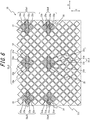
FIG. 8 is a diagram illustrating another example state of the switching unit illustrated inFIG. 1 ; -
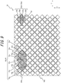
FIG. 9 is a diagram illustrating another example state of the switching unit illustrated inFIG. 1 ; and -
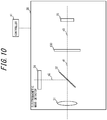
FIG. 10 is a diagram illustrating a schematic configuration of an example variation of the electromagnetic wave detection apparatus according to the embodiment. - An electromagnetic wave detection apparatus can acquire more detailed information regarding a measuring object by scanning across the measuring object using electromagnetic waves than that acquired by, for example, radiating electromagnetic waves to one spot on the measuring object. Thus, it is useful for the electromagnetic wave detection apparatus to scan across the measuring object using electromagnetic waves.
- The electromagnetic wave detection apparatus can scan across the measuring object using electromagnetic waves by changing a radiation direction of the electromagnetic waves. Here, when the radiation direction to radiate the electromagnetic waves is changed, a position (an irradiation position) on the measuring object at which the electromagnetic waves are reflected can be displaced. When the position on the measuring object at which electromagnetic waves are reflected is changed, a direction in which electromagnetic waves arrive in the electromagnetic wave detection apparatus can be changed. Accordingly, for the purpose of preventing erroneous detection, the electromagnetic wave detection apparatus uses, for example, a DMD (Digital Micro mirror Device) to selectively detect electromagnetic waves arriving from a direction corresponding to the radiation direction of the electromagnetic waves. The DMD includes a plurality of minute reflection surfaces arranged in two-dimensions. The electromagnetic wave detection apparatus switches the minute reflection surfaces corresponding to the radiation direction of electromagnetic waves, from among the plurality of minute reflection surfaces included in the DMD, to a predetermined inclined state and thus selectively detects electromagnetic waves arriving from the direction corresponding to the radiation direction of the electromagnetic waves. When scanning across the measuring object using electromagnetic waves, the electromagnetic wave detection apparatus suppresses erroneous detection by switching the minute reflection surfaces of the DMD corresponding to the radiation direction of the electromagnetic waves to the predetermined inclined state, every time the radiation direction of the electromagnetic waves is changed.
- However, when scanning across the measuring object using electromagnetic waves, switching minute reflective surfaces of the DMD corresponding to a radiation direction of electromagnetic waves to the predetermined inclined state every time the radiation direction of electromagnetic waves is changed may inhibit efficient scanning across the measuring object using electromagnetic waves.
- As such, an electromagnetic wave detection apparatus according to the present disclosure is configured to efficiently scan across a measuring object using electromagnetic waves and thus can efficiently scan across the measuring object using electromagnetic waves. Hereinafter, embodiments pertain to the present disclosure will be described with reference to the drawings.
- An electromagnetic
wave detection apparatus 1 includes anelectromagnetic wave detector 30, amemory 40, and acontroller 41, as illustrated inFIG. 1 . The electromagneticwave detection apparatus 1 may further include aradiation unit 10 and ascanner 20. - In
FIG. 1 , a broken line connecting each functional block indicates a flow of a control signal or information. A solid line protruding from each functional block indicates a flow of electromagnetic waves. - The
radiation unit 10 radiates electromagnetic waves under the control of thecontroller 41. Theradiation unit 10 may radiate at least one of infrared rays, visible rays, ultraviolet rays, and radio waves. In the present embodiment, theradiation unit 10 radiates infrared rays. Electromagnetic waves radiated from theradiation unit 10 is radiated to anobject 2 via thescanner 20. - The radiation region 11 may include at least one of a laser diode (LD: Laser Diode), a light emitting diode (LED: Light Emitting Diode), a vertical cavity surface emitting laser (VCSEL: Vertical Cavity Surface Emitting Laser), a photonic crystal laser, a gas laser, and a fiber laser. In the present embodiment, the
radiation unit 10 includes a laser diode. An example of the laser diode may include a Fabry-Perot laser diode or the like. - The
scanner 20 changes a direction of electromagnetic waves radiated from theradiation unit 10, based on the control by thecontroller 41. Electromagnetic waves whose direction is changed by the scanner is radiated toward theobject 2. Thescanner 20 may include any one of an MEMS mirror, a galvano mirror, and a polygon mirror. In the present embodiment, thescanner 20 includes a biaxial MEMS mirror. - The
scanner 20 changes a direction of electromagnetic waves by reflecting the electromagnetic waves radiated by theradiation unit 10. Thescanner 20 can rotate about anaxis 21 and anaxis 22 orthogonal to each other, as respectively illustrated inFIG. 2 andFIG. 3 . - The
scanner 20 changes a reflecting direction of electromagnetic waves by rotating about theaxis 21, as illustrated inFIG. 2 . The electromagneticwave detection apparatus 1 configured in this manner can scan across theobject 2 using electromagnetic waves along a direction A orthogonal to theaxis 21. - The
scanner 20 changes the reflecting direction of electromagnetic waves by rotating about theaxis 22, as illustrated inFIG. 3 . The electromagneticwave detection apparatus 1 configured in this manner can scan across theobject 2 using electromagnetic waves along a direction B orthogonal to theaxis 22. - An irradiation position of electromagnetic waves on the
object 2 is displaced according to the direction of the electromagnetic waves changed by thescanner 20. For example, when thescanner 20 changes a direction of electromagnetic waves as illustrated inFIG. 2 , the irradiation position of the electromagnetic waves on theobject 2 can be displaced between a position PI, a position P2, and a position P3. When the irradiation position of the electromagnetic waves on theobject 2 is displaced, the direction in which the electromagnetic waves arrive at theelectromagnetic wave detector 30 may change. As illustrated inFIG. 2 , for example, a direction in which electromagnetic waves reflected at the position P1 arrive at theelectromagnetic wave detector 30, a direction in which electromagnetic wave reflected at the position P2 arrive at theelectromagnetic wave detector 30, and a direction in which electromagnetic waves reflected at the position P3 arrive at theelectromagnetic wave detector 30 are different from one another. - The
scanner 20 may include an angle sensor such as, for example, an encoder. In this configuration, thescanner 20 may notify thecontroller 41 of an angle detected by the angle sensor as direction information used for reflecting electromagnetic waves. In such a configuration, thecontroller 41 can calculate the irradiation position on theobject 2, based on the direction information acquired from thescanner 20. Thecontroller 41 can calculate the irradiation position on theobject 2, based on a driving signal input to thescanner 20 to change the reflecting direction of electromagnetic waves. - The
electromagnetic wave detector 30 includes a front-stageoptical system 31, a switchingunit 33, a rear-stageoptical system 34, and afirst detector 35, as illustrated inFIG. 1 . Theelectromagnetic wave detector 30 may further include aseparator 32 and asecond detector 36. - The front-stage
optical system 31 forms an image of theobject 2. The front-stageoptical system 31 may include at least one of a lens and a mirror. - The
separator 32 is arranged between the front-stageoptical system 31 and a primary image forming position where the front-stageoptical system 31 forms an image of theobject 2 that is located at a predetermined distance from the front-stageoptical system 31. Theseparator 32 is configured to separate incident electromagnetic waves into electromagnetic waves to progress in a progression direction d1 toward the switchingunit 33 and electromagnetic waves to progress in a progression direction d2 (a third direction) toward thesecond detector 36. - In one embodiment, the
separator 32 reflects a part of incident electromagnetic waves in the progression direction d2 and transmits another part of the incident electromagnetic waves in the progression direction d1. Theseparator 32 may transmit a part of incident electromagnetic waves in the progression direction d1 and transmit another part of the incident electromagnetic waves in the progression direction d2. Further, theseparator 32 may refract a part of incident electromagnetic waves in the progression direction d1 and refract another part of the incident electromagnetic waves in the progression direction d2. Theseparator 32 may include at least one of a half mirror, a beam splitter, a dichroic mirror, a cold mirror, a hot mirror, a metasurface, a deflection element, and a prism. - The switching
unit 33 is arranged on a path of electromagnetic waves progressing in the progression direction d1 from theseparator 32. Further, the switchingunit 33 is located at or in the vicinity of the primary image forming position where the front-stageoptical system 31 forms an image of theobject 2 that is located at the predetermined distance from the front-stageoptical system 31, in the progression direction d1 from theseparator 32. In the present embodiment, the switchingunit 33 is arranged at the image forming position. - The switching
unit 33 has areference surface 33s on which electromagnetic waves having passed through the front-stageoptical system 31 and theseparator 32 are to be incident. Thereference surface 33s includes a plurality of switchingelements 33a arranged in two-dimensions. Thereference surface 33s is a surface that causes an action such as, for example, reflection or transmission of electromagnetic waves in at least one of a first state and a second state, which will be described later. - The switching
unit 33 can switch electromagnetic waves incident on thereference surface 33s having progressed in the progression direction d1 between the first state for causing the electromagnetic waves to progress in an on-direction d3 (a first direction) and the second state for directing the electromagnetic waves to progress in an off-direction d4 (a second direction), for each of theswitching elements 33a. In the present embodiment, the first state is a first reflection state for reflecting the electromagnetic waves incident on thereference surface 33s in the on-direction d3. Also, the second state is a second reflection state for causing the electromagnetic waves incident on thereference surface 33s to progress in the off-direction d4. - In the present embodiment, the switching
unit 33 includes a reflection surface for reflecting electromagnetic waves for each of theswitching elements 33a. The switchingunit 33 switches between the first reflection state and the second reflection state for each of theswitching elements 33a by changing a direction of the reflection surface for each of theswitching elements 33a. - The switching
unit 33 switches each of theswitching elements 33a between the first state and the second state, based on the control by thecontroller 41. For example, the switchingunit 33 can cause electromagnetic waves incident on a switching element 33a1 to progress in the on-direction d3 by switching the switching elements 33a1 to the first state, as illustrated inFIG. 1 . Simultaneously, the switchingunit 33 can cause electromagnetic waves incident on a switching element 33a2 to progress in the off-direction d4 by switching the switching element 33a2 to the second state. - In the present embodiment, the switching
unit 33 includes a DMD The DMD can switch between an inclination state in which the minute reflection surface for each of theswitching element 33a is inclined at +12 degrees and an inclination state in which the minute reflection surface for each of theswitching element 33a is inclined at -12 degrees, both with respect to thereference surface 33s, by driving the minute reflection surfaces constituting thereference surface 33s. Thereference surface 33s is parallel to a plate surface of a substrate having the minute reflection surfaces of the DMD mounted thereon. The minute reflection surfaces of the DMD are also referred to as micromirror surfaces (micromirrors). In other words, theswitching elements 33a include the respective micromirror surfaces (the micromirrors). - The plurality of switching
elements 33a are arranged in a square grid pattern on thereference surface 33s, as illustrated inFIG. 4 . Theswitching elements 33a include the respective quadrangular reflection surfaces. Theswitching elements 33a include therespective rotation axes 33b. The rotation axes 33b extend along a diagonal line of the quadrangular reflection surfaces, i.e., the micromirror surfaces. Theswitching elements 33a are switched between the inclination state to be inclined at +12 degrees about therotation axis 33b with respect to thereference surface 33s and the inclination state to be inclined at -12 degrees about therotation axis 33b with respect to thereference surface 33s. An extending direction of the rotation axes 33b of theswitching elements 33a may be appropriately determined in consideration of the position of a detection surface of thefirst detector 35 illustrated inFIG. 1 . - A spot S0 can be formed on the
switching unit 33, as illustrated inFIG. 4 . The spot S0 is a spot of electromagnetic waves formed on theswitching unit 33 by incident electromagnetic waves reflected by theobject 2, from among electromagnetic waves radiated by theradiation unit 10 illustrated inFIG. 1 . A position of the spot S0 on theswitching unit 33 can be displaced according to the direction in which electromagnetic waves arrive in theelectromagnetic wave detector 30. Here, when a direction of electromagnetic waves reflected by thescanner 20 is changed as described above with reference toFIG. 2 andFIG. 3 , the irradiation position of electromagnetic waves on theobject 2 is displaced, whereby a direction in which the electromagnetic waves arrive at theelectromagnetic wave detector 30 can be changed. That is, the position of the spot S0 on theswitching unit 33 can be displaced according to the irradiation position of electromagnetic waves on theobject 2. For example, when the irradiation position of electromagnetic waves on theobject 2 is displaced along the direction A as illustrated inFIG. 2 , the spot S0 is displaced along a direction D illustrated inFIG. 4 . For example, when the irradiation position of electromagnetic waves on theobject 2 is displaced along the direction B as illustrated inFIG. 3 , the position of the spot S0 is displaced along a direction C illustrated inFIG. 4 . - The spot S0 may have, for example, an elliptical shape, depending on a shape of a portion of the
radiation unit 10 for emitting light. In another embodiment, the spot S0 may have a rectangular shape. In the present embodiment, a longitudinal direction of the elliptical spot S0 having the elliptical shape extends along the direction C. Further, a transverse direction of the spot S0 having the elliptical shape extends along the direction D. - The
switching elements 33a are switched to the first state, based on the control by thecontroller 41, as described above. For example, before the spot S0 illustrated inFIG. 4 is formed, four switchingelements 33a are switched to the first state, based on the control by thecontroller 41. Each of the fourswitching elements 33a includes a part of the spot S0. In this configuration, electromagnetic waves having formed the spot S0 can be reflected by the fourswitching elements 33a and can progress in the on-direction d3 illustrated inFIG. 1 . In the subsequent drawings, theswitching elements 33a in the first state are hatched. - The
rotation axis 33b of theswitching element 33a may extend along the direction D corresponding to the longitudinal direction of the spot S0 illustrated inFIG. 4 . - As illustrated in
FIG. 1 , the rear-stageoptical system 34 is arranged on a path of electromagnetic waves progressing in the on-direction d3 from the switchingunit 33. The rear-stageoptical system 34 may include at least one of a lens and a mirror. The rear-stageoptical system 34 forms an image of theobject 2 as electromagnetic waves whose progression direction is switched by the switchingunit 33. - The
first detector 35 is arranged on a path of electromagnetic waves progressing via the rear-stageoptical system 34 after being caused to progress in the on-direction d3 by the switchingunit 33. Thefirst detector 35 detects electromagnetic waves having passed through the rear-stageoptical system 34, that is, electromagnetic waves progressing in the on-direction d3 (the first direction). - In the present embodiment, the
first detector 35 is an active sensor configured to detect electromagnetic waves (reflected waves) reflected by theobject 2, from among electromagnetic waves radiated to theobject 2 by theradiation unit 10 and thescanner 20. - In the present embodiment, the
first detector 35 includes an element constituting a distance sensor. For example, thefirst detector 35 includes one element such as an APD (Avalanche Photodiode), a PD (Photodiode), a SiPM (Silicon Photomultiplier), a SPAD (Single Photon Avalanche Diode), or a distance image sensor. Thefirst detector 35 may include an element array such as an APD array, a PD array, a distance imaging array, or a distance image sensor. Thefirst detector 35 may include an image sensor or a temperature sensor, which will be described later. - In the present embodiment, the
first detector 35 transmits detection information indicating that electromagnetic waves reflected by theobject 2 are detected, as a signal to thecontroller 41. Thefirst detector 35 detects electromagnetic waves in the infrared band. - Note that the
first detector 35 simply needs to be able to detect electromagnetic waves in a configuration in which thefirst detector 35 is one element constituting the distance measuring sensor mentioned above. That is, thefirst detector 35 does not need to form an image on its detection surface. Thus, thefirst detector 35 does not need to be arranged at a secondary image forming position where the rear-stageoptical system 34 forms an image. In this configuration, in other words, thefirst detector 35 may be arranged at any location on a path of electromagnetic waves that progress via the rear-stageoptical system 34 after being caused to progress in the on-direction d3 by the switchingunit 33, so long as allowing electromagnetic waves progressing from all angles of view to be incident on the detection surface of thefirst detector 35. - The
second detector 36 is arranged on a path of electromagnetic waves progressing in the progression direction d2 from theseparator 32. Further, thesecond detector 36 is located at or in the vicinity of an image forming position where the front-stageoptical system 31 forms an image of theobject 2 that is located at a predetermined distance from the front-stageoptical system 31, in the progression direction d2 from theseparator 32. Thesecond detector 36 detects electromagnetic waves progressing in the progression direction d2 from theseparator 32. Thesecond detector 36 detects electromagnetic waves of a different type or the same type as electromagnetic waves detected by thefirst detector 35. - In the present embodiment, the
second detector 36 is a passive sensor. Thesecond detector 36 may be a sensor of a different type or the same type as thefirst detector 35. Thesecond detector 36 may include an element array. For example, thesecond detector 36 includes an image sensor or imaging array, captures an image of electromagnetic waves formed on the detection surface, and generates image information corresponding to the capturedobject 2. - In the present embodiment, the
second detector 36 captures an image of visible light. Thesecond detector 36 transmits generated image information as a signal to thecontroller 41. - The
second detector 36 may capture an image of infrared light, ultraviolet, radio waves, or the like rather than an image of visible light. Further, thesecond detector 36 may include a distance measuring sensor. In this configuration, the electromagneticwave detection apparatus 1 can acquire distance information in the form of an image using thesecond detector 36. Thesecond detector 36 may include a temperature sensor or the like. In this configuration, the electromagneticwave detection apparatus 1 can acquire temperature information in the form of an image using thesecond detector 36. - The
memory 40 illustrated inFIG. 1 may include one or more memories. Thememory 40 may function as a primary storage device or a secondary storage device. Thememory 40 stores any information and program used for an operation of the electromagneticwave detection apparatus 1. Thememory 40 may be included in thecontroller 41. - For example, the
memory 40 stores a deflection pattern and a radiation pattern. The deflection pattern includes information regarding a direction in which thescanner 20 reflects electromagnetic waves when thescanner 20 changes a direction of electromagnetic waves radiated by theradiation unit 10. The radiation pattern includes timing information used for causing theradiation unit 10 to radiate electromagnetic waves. Further, thememory 40 stores the deflection pattern and the radiation pattern in association with position information of asubdivision 33u, which will be described later. - The
controller 41 illustrated inFIG. 1 includes one or more processors. The processor may include at least one of a general purpose processor configured to read a specific program and perform a specific function, and a specialized processor dedicated for specific processing. The specialized processor may include an ASIC (Application Specific Integrated Circuit). The processor may include a PLD (Programmable Logic Device). The PLD may include an FPGA (Field-Programmable Gate Array). Thecontroller 41 may include at least one of a SoC (System-on-a-Chip) that includes one or more cooperating processors and a SiP (System in a Package). - First, the
controller 41 acquires the deflection pattern and the radiation pattern from thememory 40. As illustrated inFIG. 2 , the deflection pattern is a pattern in which thescanner 20 rotates about theaxis 21 and deflects electromagnetic waves radiated by theradiation unit 10 along the direction A illustrated inFIG. 2 . The radiation pattern is a pattern in which theradiation unit 10 radiates electromagnetic waves three times at predetermined intervals. When thecontroller 41 controls theradiation unit 10 and thescanner 20 according to the deflection pattern and the radiation pattern, electromagnetic waves are sequentially irradiated to positions PI, P2, and P3 on theobject 2 illustrated inFIG. 2 . The positions PI, P2, and P3 are located on theobject 2 in a linear manner and separated from one another along the direction A. Electromagnetic waves reflected at the position P1 illustrated inFIG. 2 forms a spot S1 illustrated inFIG. 5 . Similarly, electromagnetic waves reflected at the position P2 and the position P3 illustrated inFIG. 2 respectively form the spot S2 and the spot S3 illustrated inFIG. 5 . The spot S1 illustrated inFIG. 5 is formed at the image forming position on thereference surface 33s at the position P1 illustrated inFIG. 2 by the front-stageoptical system 31. Similarly, the spot S2 and the spot S3 illustrated inFIG. 5 are formed at the image forming positions on thereference surface 33s at the position P2 and the position P3 illustrated inFIG. 2 by the front-stageoptical system 31. Because electromagnetic waves are sequentially irradiated to the positions P1, P2, and P3 illustrated inFIG. 2 as described above, the spots S1, S2, and S3 illustrated inFIG. 5 are sequentially formed on theswitching unit 33. Because the positions P1, P2, and P3 illustrated inFIG. 2 are located on the same straight line, the spots S1, S2, and S3 are located in the same position with respect to the direction C. In the present embodiment, the spots S1 to S3 and the like formed on theswitching unit 33 have the same shapes. - Next, the
controller 41 acquires position information of a plurality ofsubdivisions 33u associated with the deflection pattern and the radiation pattern described above from thememory 40. Further, thecontroller 41 causes theswitching unit 33 to simultaneously set some of the plurality ofsubdivisions 33u to the first state. In this configuration, the some of the plurality ofsubdivisions 33u are subdivisions 33u1, 33u2, 33u3 illustrated inFIG. 5 . The subdivisions 33u1 to 33u3 are located apart from one another along the direction D serving as at least one direction of thereference surface 33s. The subdivisions 33u1 to 33u3 are located at respective positions on theswitching unit 33 where the spots S1 to S3 are formed. Theswitching elements 33a included in the subdivision 33u1 are arranged in a manner including the spot S1 of electromagnetic waves that can be formed in the subdivision 33u1. In other words, each of the fourswitching elements 33a included in the subdivision 33u1 includes a part of the spot S1 formed on theswitching unit 33. Similarly, theswitching elements 33a included in each of the subdivisions 33u2 and 33u3 are arranged in a manner respectively including the electromagnetic wave spots S2 and S3 formed in the subdivisions 33u2 and 33u3. In other words, each of the fourswitching elements 33a included in the subdivisions 33u2 includes a part of the spot S2 that can be formed on theswitching unit 33, and each of the fourswitching elements 33a included in the subdivision 33u3 includes a part of the spot S3 that can be formed on theswitching unit 33. - Subsequently, the
controller 41 radiates electromagnetic waves to the position P1 on theobject 2 illustrated inFIG. 2 by controlling theradiation unit 10 and thescanner 20. The electromagnetic waves reflected at the position P1 illustrated inFIG. 2 forms the spot S1 illustrated inFIG. 5 . The electromagnetic wave having formed the spot S1 can be reflected by the fourswitching elements 33a included in the subdivision 33u1, can progress in the on-direction d3 illustrated inFIG. 1 , and can then be incident on thefirst detector 35 illustrated inFIG. 1 . Further, by settingswitching elements 33a located around the subdivision 33u1 to the second state, incidence of ambient light on thefirst detector 35 illustrated inFIG. 1 can be suppressed. Then, thecontroller 41 may quickly switch theswitching elements 33a included in the subdivision 33u1 to the second state. - Also, the
controller 41 radiates electromagnetic waves to the position P2 of theobject 2 illustrated inFIG. 2 by controlling theradiation unit 10 and thescanner 20. The electromagnetic waves reflected at the position P2 illustrated inFIG. 2 forms the spot S2 illustrated inFIG. 5 . The electromagnetic waves having formed the spot S2 can be reflected by the fourswitching elements 33a included in the subdivision 33u2, can progress in the on-direction d3 illustrated inFIG. 1 , and can then be incident on thefirst detector 35 illustrated inFIG. 1 . Further, by settingswitching elements 33a located around the subdivision 33u2 to the second state, incidence of ambient light on thefirst detector 35 illustrated inFIG. 1 can be suppressed. Then, thecontroller 41 may quickly switch theswitching elements 33a included in the subdivision 33u2 to the second state. - Further, the
controller 41 radiates electromagnetic waves to the position P3 of theobject 2 illustrated inFIG. 2 by controlling theradiation unit 10 and thescanner 20. The electromagnetic waves reflected at the position P3 illustrated inFIG. 2 forms the spot S3 illustrated inFIG. 5 . The electromagnetic waves having formed the spot S3 can be reflected by the fourswitching elements 33a included in the subdivision 33u3, can progress in the on-direction d3 illustrated inFIG. 1 , and can then be incident on thefirst detector 35 illustrated inFIG. 1 . Further, by settingswitching elements 33a located around the subdivision 33u3 to the second state, incidence of ambient light on thefirst detector 35 illustrated inFIG. 1 can be suppressed. Then, thecontroller 41 may quickly switch theswitching elements 33a included in the subdivision 33u3 to the second state. - In the present embodiment, as described above, the
controller 41 causes theswitching unit 33 to simultaneously set the subdivisions 33u1 to 33u3 located at the locations where the spots S1 to S3 are formed into the first state in advance. In this present embodiment, this configuration eliminates the necessity for thecontroller 41 to switch theswitching elements 33a to the first state or the second state every time the radiation direction of electromagnetic waves is changed. Thus, the electromagneticwave detection apparatus 1 according to the present embodiment can efficiently scan across theobject 2 using electromagnetic waves. - As illustrated in
FIG. 5 , a distance between the subdivision 33u1 and the subdivision 33u2 in the direction D and a distance between the subdivision 33u2 and the subdivision 33u3 in the direction D may be equal to or longer than a length of the spot S1 along the direction D. This configuration can more reliably suppress incidence of ambient light on thefirst detector 35 illustrated inFIG. 1 . - Further, the
controller 41 may reduce or increase the number of thesubdivisions 33u that are to be simultaneously set to the first state in advance. For example, in a case in which there is concern about an influence of ambient light due to a measuring environment, thecontroller 41 may reduce the number of thesubdivisions 33u to be simultaneously set to the first state, based on an order of the spots formed on theswitching unit 33. In a configuration illustrated inFIG. 5 , the spots S1 to S3 are sequentially formed on theswitching unit 33. In this configuration, thecontroller 41 may simultaneously set the subdivisions 33u1 and 33u2 to the first state in advance and set the subdivisions 33u3 to the second state. Further, thecontroller 41 may form, for example, the spot S1 on theswitching unit 33 by radiating electromagnetic waves to the position P1 illustrated inFIG. 2 and then switch the subdivision 33u3 to the first state. This configuration can more reliably suppress incidence of ambient light on thefirst detector 35 illustrated inFIG. 1 . - There are various patterns for the control described above. Hereinafter, other examples of such various patterns will be described.
- In Example 1, electromagnetic waves are radiated from the electromagnetic
wave detection apparatus 1 to theobject 2 so that the spots S1, S2, S3, S4, S5, and S6 are formed on theswitching unit 33 as illustrated inFIG. 6 . The spots S4 to S6 are located apart from one another along the direction D. The spots S4 to S6 are in the same locations with respect to the direction C. The spots S1 and spot S4 are in the same locations with respect to the direction D. The spot S2 and the spot S5 are in the same locations with respect to the direction D. The spot S3 and the spot S6 are in the same locations with respect to the direction D. A distance between the spots S1 to S3 arranged along the direction D and the spots S4 to S6 arranged along the direction D is smaller than a distance between the spot S1 and the spot S2 in the direction D. - In Example 1, the
controller 41 may simultaneously set the subdivisions 33u1, 33u2, 33u3, 33u4, 33u5, and 33u6 to the first state, as illustrated inFIG. 6 . - The subdivision 33u4 includes four
switching elements 33a located adjacent to one another, as illustrated inFIG. 6 . Each of the fourswitching elements 33a included in the subdivision 33u4 includes a part of the spot S4. The subdivision 33u3 and the subdivision 33u4 are in the same location with respect to the direction D. A distance between the subdivision 33u3 and the subdivision 33u4 in the direction C may be equal to or longer than a length of the spot S1 along the direction C. - The subdivision 33u5 includes four
switching elements 33a located adjacent to one another, as illustrated inFIG. 6 . Each of the fourswitching elements 33a included in the subdivision 33u5 includes a part of the spot S5. The subdivision 33u2 and the subdivision 33u5 are in the same location with respect to the direction D. A distance between the subdivision 33u2 and the subdivision 33u5 in the direction C may be equal to or longer than the length of the spot S1 along the direction C. - The subdivision 33u5 includes four
switching elements 33a located adjacent to one another, as illustrated inFIG. 6 . Each of the fourswitching elements 33a included in the subdivision 33u6 includes a part of the spot S6. The subdivision 33u1 and the subdivision 33u6 are in the same location with respect to the direction D. A distance between the subdivision 33u1 and the subdivision 33u6 in the direction C may be equal to or longer than the length of the spot S1 along the direction C. - The
controller 41 may cause theswitching unit 33 to sequentially form the spots S1 to S6 by controlling theradiation unit 10 and thescanner 20. In particular, thecontroller 41 may cause theradiation unit 10 to radiate electromagnetic waves three times at the predetermined intervals and, simultaneously, cause thescanner 20 to rotate about theaxis 21 as illustrated inFIG. 2 . By this configuration, the spots S1 to S3 can be formed on theswitching unit 33. Then, thecontroller 41 causes thescanner 20 to rotate about theaxis 22 as illustrated inFIG. 3 . Further, thecontroller 41 causes theradiation unit 10 to radiate electromagnetic waves three times at the predetermined intervals and, simultaneously, causes thescanner 20 to rotate about theaxis 21 as illustrated inFIG. 2 . By this configuration, the spots S4 to S6 can be formed on theswitching unit 33. - In a configuration illustrated in
FIG. 6 , thecontroller 41 may reduce or increase the number of thesubdivisions 33u that are to be simultaneously set to the first state as described above with reference toFIG. 5 . - In Example 2, electromagnetic waves are radiated from the electromagnetic
wave detection apparatus 1 to theobject 2 so that spots S1, S2, S3, S7, and S8 are formed on theswitching unit 33 as illustrated inFIG. 7 . The spot S7 and the spot S8 are located apart from each other in the direction D. The spot S7 and the spot S8 are in the same location with respect to the direction C. The spot S7 is located between the spot S2 and the spot S3 in the direction D. The spot S8 is located between the spot S1 and the spot S2 in the direction D. - In Example 2, the
controller 41 may simultaneously set the subdivisions 33u1, 33u2, 33u3, 33u7, and 33u8 to the first state. - As illustrated in
FIG. 7 , the subdivision 33u7 includes fourswitching elements 33a located adjacent to one another. Each of the fourswitching elements 33a included in the subdivision 33u7 includes a part of the spot S7. The subdivision 33u7 is located between the subdivision 33u2 and the subdivision 33u3 in the direction D. A part of the subdivision 33u7, a part of the subdivision 33u2, and a part of the subdivision 33u3 may overlap with one another in the direction C. - As illustrated in
FIG. 7 , the subdivision 33u8 includes fourswitching elements 33a located adjacent to one another. Each of the fourswitching elements 33a included in the subdivision 33u8 includes a part of the spot S8. The subdivision 33u8 is located between the subdivision 33u1 and the subdivision 33u2 in the direction D. A part of the subdivision 33u8, a part of the subdivision 33u1 and a part of the subdivision 33u2 may overlap with one another in the direction C. - In a configuration illustrated in
FIG. 7 , thecontroller 41 may cause theswitching unit 33 to sequentially form the spots S1 to S3, S7, and S8 by controlling theradiation unit 10 and thescanner 20. In particular, thecontroller 41 causes theradiation unit 10 to radiate electromagnetic waves three times at predetermined intervals and, simultaneously, causes thescanner 20 to rotate about theaxis 21 as illustrated inFIG. 2 . By this configuration, the spots S1 to S3 can be formed on theswitching unit 33. Then, thecontroller 41 causes thescanner 20 to rotate about theaxis 22 as illustrated inFIG. 3 . Further, thecontroller 41 causes theradiation unit 10 to radiate electromagnetic waves two times at predetermined intervals and, simultaneously, causes thescanner 20 to rotate about theaxis 21 as illustrated inFIG. 2 . By this configuration, the spots S7 and S8 can be formed on theswitching unit 33. - In the configuration illustrated in
FIG. 7 , thecontroller 41 may reduce or increase the number of thesubdivisions 33u that are to be simultaneously set to the first state as described above with reference toFIG. 5 . - In Example 3, electromagnetic waves are radiated from the electromagnetic
wave detection apparatus 1 to theobject 2 so that the spot S1 and a spot S9 are formed on theswitching unit 33 as illustrated inFIG. 8 . The spot S1 and the spot S9 are located apart from each other along a direction inclined with respect to the direction D. - In Example 3, the
controller 41 may simultaneously set the subdivisions 33u1 and 33u9 to the first state, as illustrated inFIG. 8 . - The subdivision 33u9 includes four
switching elements 33a located adjacent to one another, as illustrated inFIG. 8 . Each of the fourswitching elements 33a included in the subdivision 33u9 includes a part of the spot S9. The subdivision 33u1 and the subdivision 33u9 are located apart from each other along the direction inclined with respect to the direction D serving as at least one direction of thereference surface 33s. - In a configuration illustrated in
FIG. 8 , thecontroller 41 may cause theswitching unit 33 to sequentially form the spot S1 and the spot S9 by controlling theradiation unit 10 and thescanner 20. In particular, thecontroller 41 causes theradiation unit 10 to radiate electromagnetic waves one time. By this configuration, the spot S1 is formed on theswitching unit 33. Also, thecontroller 41 causes thescanner 20 to rotate about theaxis 21 and theaxis 22 as respectively illustrated inFIG. 2 andFIG. 3 . Further, thecontroller 41 causes theradiation unit 10 to radiate electromagnetic waves one time. By this configuration, the spot S9 is formed on theswitching unit 33. - In the configuration illustrated in
FIG. 8 , thecontroller 41 may reduce or increase the number of thesubdivisions 33u that are to be simultaneously set to the first state as described above with reference toFIG. 5 . - The
controller 41 acquires information regarding the surroundings of the electromagneticwave detection apparatus 1, based on electromagnetic waves detected by each of thefirst detector 35 and thesecond detector 36, that is, detection results by thefirst detector 35 and thesecond detector 36. The information regarding the surroundings is, for example, image information, distance information, temperature information, or the like. Thecontroller 41 acquires the image information using thesecond detector 36. Further, thecontroller 41 acquires the distance information using thefirst detector 35, as will be described later. - For example, the
controller 41 acquires the distance information using a ToF (Time-of-Flight) method. In this configuration, the controller 14 may include a time measurement LSI (Large Scale Integrated circuit). By using the time measurement LSI, thecontroller 41 measures a time ΔT from time at which theradiation unit 10 is caused to radiate electromagnetic waves to time at which the detection information is acquired by thefirst detector 35. Thecontroller 41 calculates a distance to the irradiation position on theobject 2 by multiplying the measured time ΔT by the speed of light and then dividing an acquired result by 2. Thecontroller 41 calculates the irradiation position of electromagnetic waves, based on the direction information acquired from thescanner 20, the driving signal output to thescanner 20 by thecontroller 41, or a driving signal output to each of theradiation unit 10. Thecontroller 41 acquires the distance information in the form of an image by calculating a distance to each irradiation position while changing the irradiation position of electromagnetic waves. - In the present embodiment, the electromagnetic
wave detection apparatus 1 is configured to acquire distance information using Direct ToF that directly measures time from radiation of electromagnetic waves to return of the electromagnetic waves. However, the configuration of the electromagneticwave detection apparatus 1 is not limited thereto. For example, the electromagneticwave detection apparatus 1 may acquire distance information using Flash ToF that indirectly measures time from radiation of electromagnetic waves at fixed intervals to return of the electromagnetic waves, based on a phase difference between the radiated electronic waves and the returned electromagnetic waves. Alternatively, the electromagneticwave detection apparatus 1 may acquire distance information using another ToF method such as, for example, Phased ToF. - Here, time required to scan the
object 2 using electromagnetic waves can be restricted by the following time (1) to time (3): (1) time necessary for electromagnetic waves radiated from theradiation unit 10 to be reflected by theobject 2 and incident on thefirst detector 35; (2) time necessary for thescanner 20 to rotate about theaxis 21 illustrated inFIG. 2 oraxis 22 illustrated inFIG. 3 to change a direction of electromagnetic waves radiated from theradiation unit 10; (3) time necessary for the switchingunit 33 to switch theswitching elements 33a to the first state or the second state. The time required to scan theobject 2 using electromagnetic waves is most restricted by the time (3), from among the times (1) to (3). - In the electromagnetic
wave detection apparatus 1 according to the present embodiment, thecontroller 41 simultaneously sets a plurality ofsubdivisions 33u located apart from one another along at least one direction (e.g., the direction D) of thereference surface 33s to the first state. The present embodiment having this configuration eliminates the necessity for thecontroller 41 to switch theswitching elements 33a to the first state or the second state every time the radiation direction of electromagnetic waves is changed. In the present embodiment, in other words, the restriction by the time (3) described above can be reduced. The electromagneticwave detection apparatus 1 according to the present embodiment having this configuration can efficiently scan across theobject 2 using electromagnetic waves. The electromagneticwave detection apparatus 1 according to the present embodiment can increase a quantity of information that can be acquired, for example, per unit time, by efficiently scanning across theobject 2 using electromagnetic waves. - Although the embodiments according to the present disclosure have been described based on the figures and the examples, it should be apparent to those skilled in the art that various modifications and alterations can be made without departing from the present disclosure. Accordingly, such modifications and alterations are to be included in the scope of the present disclosure.
- In the present embodiment, for example, the
radiation unit 10, thescanner 20, theelectromagnetic wave detector 30, thememory 40, and thecontroller 41 have been described to constitute the electromagneticwave detection apparatus 1. However, the information acquisition system may be configured using an apparatus that includes theradiation unit 10 and thescanner 20 and an apparatus that includes theelectromagnetic wave detector 30. The information acquisition system configured in this manner may further include thememory 40 and thecontroller 41. - In the present embodiment, the electromagnetic
wave detection apparatus 1 has been described to include theradiation unit 10 and thescanner 20, as illustrated inFIG. 1 . However, elements included in the electromagneticwave detection apparatus 1 are not limited to theradiation unit 10 and thescanner 20. For example, the electromagneticwave detection apparatus 1 may include a phased array, rather than theradiation unit 10 and thescanner 20. In this configuration, the electromagneticwave detection apparatus 1 can perform grating scanning using the phased array. - In the present embodiment, the
subdivision 33u has been described to include fourswitching elements 33a located adjacent to one another, as illustrated inFIG. 5 . However, the number of theswitching elements 33a included in thesubdivision 33u is not limited to four. Thesubdivision 33u simply needs to include oneswitching element 33a. - In the present embodiment, the plurality of
subdivisions 33u has been described to include the same number of theswitching elements 33a, as illustrated inFIG. 5 . However, the plurality ofsubdivisions 33u may include different number of theswitching elements 33a. - In the present embodiment, the spots S1 and the like formed on the
switching unit 33 have been described to have the same shapes. However, the spots formed on theswitching unit 33 do not need to have the same shapes. For example, spots S1 and S10 having different sizes may be formed, as illustrated inFIG. 9 . An area of the spot S10 illustrated inFIG. 9 is approximately 2.5 times an area of the spot S1. In a configuration illustrated inFIG. 9 , thecontroller 41 may simultaneously set the subdivision 33u1 and the subdivision 33u10 to the first state. The subdivision 33u10 includes tenswitching elements 33a located adjacent to one another. - In the present embodiment, further, the switching
unit 33 has been described to be able to switch a progression direction of electromagnetic waves incident on thereference surface 33s to two directions: the on direction d3 and the off direction d4. However, the switchingunit 33 may be able to switch the progression direction to three or more directions, rather than any of the two directions. - In the present embodiment, further, the first state has been described to be the first reflection state for reflecting electromagnetic waves incident on the
reference surface 33s in the on-direction d3, and the second state has been described to be the second reflection state for reflecting the electromagnetic waves incident on thereference surface 33s in the off-direction d4. However, the first state and the second state may refer to other modes. - For example, the first state may be a transmission state in which electromagnetic waves incident on the
reference surface 33s are transmitted to progress in the on-direction d3, as illustrated inFIG. 10 . In this configuration, aswitching unit 133 may include a shutter having a reflection surface that reflects electromagnetic waves in the off-direction d4 for each of theswitching elements 33a. Theswitching unit 133 configured as described above switches each of theswitching elements 33a between the transmission state serving as the first state and the reflection state serving as the second state, by opening and closing the shutter for each of theswitching elements 33a. - An example of the
switching unit 133 configured as described above includes a switching unit that includes a MEMS shutter in which a plurality of shutters that can be opened and closed are arranged in an array. Further, theswitching unit 133 may be a switching unit that includes a liquid crystal shutter capable of switching between a reflection state for reflecting electromagnetic waves and a transmission state for transmitting electromagnetic waves, according to a liquid crystal alignment. Theswitching unit 133 configured as described above can switch between the reflection state serving as the first state and the transmission state serving as the second state for each of theswitching elements 33a by switching the liquid crystal alignment for each of theswitching elements 33a. - In the present embodiment, further, the electromagnetic
wave detection apparatus 1 has been described to have a configuration in which thescanner 20 changes a direction of electromagnetic waves radiated from theradiation unit 10, and thefirst detector 35 functions as a scanning active sensor in cooperation with thescanner 20. However, the configuration of the electromagneticwave detection apparatus 1 is not limited thereto. For example, in a case in which the electromagneticwave detection apparatus 1 has a configuration in which theradiation unit 10 includes a plurality of radiation sources capable of radiating radial electromagnetic waves and employs a phased scanning method for radiating electromagnetic waves from each of the radiation sources at phased radiation timings, an effect similar to that of the present embodiment can be obtained. Further, for example, in a case in which the electromagneticwave detection apparatus 1 has a configuration in which thescanner 20 is omitted and information is acquired by radiating radial electromagnetic waves from theradiation unit 10 without scanning, an effect similar to that of the present embodiment can be obtained. - In the present embodiment, further, the electromagnetic
wave detection apparatus 1 has been described to include thefirst detector 35 as an active sensor and thesecond detector 36 as a passive sensor. However, the configuration of the electromagneticwave detection apparatus 1 is not limited thereto. For example, in a case in which the electromagneticwave detection apparatus 1 has a configuration in which both thefirst detector 35 and the second detector 39 serve as active sensors or passive sensors, an effect similar to that of the present embodiment can be obtained. In a configuration in which both thefirst detector 35 and the second detector 39 serve as active sensors, either theradiation unit 10 orrespective radiation units 10 may radiate electromagnetic waves to theobject 2. Further, therespective radiation units 10 may radiate electromagnetic waves of the same type or different types. -
- 1 electromagnetic wave detection apparatus
- 10 radiation unit
- 12 optical system
- 20 scanner
- 30 electromagnetic wave detector
- 31 front-stage optical system
- 32 separator
- 33, 133 switching unit
- 33s reference surface
- 33a, 33a1, 33a2 switching element
- 33u, 33u1, 33u2, 33u3, 33u4, 33u5, 33u6, 33u7, 33u8, 33u9, 33u10 subdivision
- 34 rear-stage optical system
- 35 first detector
- 36 second detector
- 40 memory
- 41 controller
- d1 progression direction
- d2 progression direction (third direction)
- d3 on-direction (first direction)
- d4 off-direction (second direction)
- S0, S1, S2, S3, S4, S5, S6, S7, S8, S9, S10 spot
- A, B, C, D direction
Claims (29)
- An electromagnetic wave detection apparatus comprising:a switching unit including a plurality of subdivisions that are arranged on a reference surface and can be switched to a first state for causing incident electromagnetic waves to progress in a first direction;a controller configured to simultaneously set some of the plurality of subdivisions located apart from one another along at least one direction of the reference surface, from among the plurality of subdivisions, to the first state; anda first detector configured to detect electromagnetic waves progressing in the first direction.
- The electromagnetic wave detection apparatus according to claim 1,
wherein a distance between the some of the plurality of subdivisions in the at least one direction in the reference surface is equal to or longer than a length of a spot of electromagnetic waves formed by the electromagnetic waves incident on the reference surface along the direction. - The electromagnetic wave detection apparatus according to claim 2,
wherein the spot has an elliptical shape, and
the at least one direction in the reference surface extends along a longitudinal direction of the spot having the elliptical shape. - The electromagnetic wave detection apparatus according to any one of claims 1 to 3,
wherein the some of the plurality of subdivisions include a plurality of switching elements that can be switched to the first state and are located adjacent to one another. - The electromagnetic wave detection apparatus according to claim 4,
wherein each of the some of the plurality of subdivisions include the same number of switching elements. - The electromagnetic wave detection apparatus according to claim 4 or 5,
wherein the switching elements included in the some of the plurality of subdivisions are arranged in a manner including a spot of electromagnetic waves formed on the subdivisions. - The electromagnetic wave detection apparatus according to any one of claims 1 to 3,
wherein the some of the plurality of subdivisions include one switching element that can be switched to the first state. - The electromagnetic wave detection apparatus according to any one of claims 4 to 6,
wherein the switching unit includes a digital micromirror device. - The electromagnetic wave detection apparatus according to any one of claims 4 to 6,
wherein the switching unit is configured to switch each of the switching elements between a transmission state for transmitting incident electromagnetic waves reflected by an object in the first direction and a reflection state for reflecting the incident electromagnetic waves in a second direction. - The electromagnetic wave detection apparatus according to claim 9,
wherein the switching unit includes a shutter having a reflection surface configured to reflect electromagnetic waves for each of the switching elements and is configured to switch between the reflection state and the transmission state by opening and closing the shutter for each of the switching elements. - The electromagnetic wave detection apparatus according to claim 10,
wherein the switching unit includes a MEMS shutter in which the shutters are arranged in an array. - The electromagnetic wave detection apparatus according to claim 9 or 10,
wherein the switching unit includes a liquid crystal shutter capable of switching between a reflection state for reflecting electromagnetic waves and a transmission state for transmitting electromagnetic waves, in accordance with a liquid crystal alignment. - The electromagnetic wave detection apparatus according to any one of claims 1 to 12, further comprising:a separator configured to separate incident electromagnetic waves into electromagnetic waves to progress in a direction toward the switching unit and electromagnetic waves to progress in a third direction; anda second detector configured to detect electromagnetic waves progressing in the third direction.
- The electromagnetic wave detection apparatus according to claim 13,
wherein the separator includes at least one of a half mirror, a beam splitter, a dichroic mirror, a cold mirror, a hot mirror, and a metasurface. - The electromagnetic wave detection apparatus according to claim 13 or 14,
wherein each of the first detector and the second detector includes at least one of a distance measuring sensor, an image sensor, and a temperature sensor. - The electromagnetic wave detection apparatus according to any one of claims 13 to 15,
wherein the first detector and the second detector are configured to detect electromagnetic waves of the same type or different types. - The electromagnetic wave detection apparatus according to any one of claims 13 to 16,
wherein each of the first detector and the second detector are configured to detect at least one of infrared rays, visible rays, ultraviolet rays, and radio waves. - The electromagnetic wave detection apparatus according to any one of claims 13 to 17,
wherein each of the first detector and the second detector includes an active sensor configured to detect reflected waves of electromagnetic waves radiated to an object from a radiation unit and incident from the object, or a passive sensor. - The electromagnetic wave detection apparatus according to any one of claims 13 to 18,
wherein each of the first detector and the second detector includes an active sensor configured to detect reflected waves of electromagnetic waves that are radiated to an object from different radiation units or the same radiation unit and incident from the object. - The electromagnetic wave detection apparatus according to claim 19,
wherein each of the different radiation units radiate electromagnetic waves of different types or the same type. - The electromagnetic wave detection apparatus according to any one of claims 18 to 20, further comprising:
the radiation unit. - The electromagnetic wave detection apparatus according to any one of claims 18 to 21,
wherein the radiation unit is configured to radiate any one of infrared rays, visible rays, ultraviolet rays, and radio waves. - The electromagnetic wave detection apparatus according to any one of claims 18 to 22,
wherein the radiation unit is configured to scan using electromagnetic waves by employing a phased scanning method. - The electromagnetic wave detection apparatus according to any one of claims 18 to 23, further comprising:
a scanner configured to scan using electromagnetic waves radiated from the radiation unit. - The electromagnetic wave detecting apparatus according to claim 24,
wherein the scanner includes a reflection surface configured to reflect electromagnetic waves and is configured to scan by reflecting electromagnetic waves radiated from the radiation unit on the reference surface while changing a direction of the reflection surface. - The electromagnetic wave detection apparatus according to claim 24 or 25,
wherein the scanner includes any one of a MEMS mirror, a galvano mirror, and a polygon mirror. - The electromagnetic wave detection apparatus according to any one of claims 13 to 26,
wherein the controller is configured to acquire information regarding surroundings, based on detection results of electromagnetic waves by the first detector and the second detector. - The electromagnetic wave detection apparatus according to claim 27,
wherein the controller is configured to acquire at least one of image information, distance information, and temperature information, as the information regarding the surroundings. - An information acquisition system comprising:a switching unit including a plurality of subdivisions that are arranged on a reference surface and can be switched to a first state for causing incident electromagnetic waves to progress in a first direction;a controller configured to simultaneously set some of the plurality of subdivisions located apart from one another along at least one direction of the reference surface, from among the plurality of subdivisions, to the first state; anda first detector configured to detect electromagnetic waves progressing in the first direction.
Applications Claiming Priority (2)
| Application Number | Priority Date | Filing Date | Title |
|---|---|---|---|
| JP2018190463A JP7004632B2 (en) | 2018-10-05 | 2018-10-05 | Electromagnetic wave detection device |
| PCT/JP2019/037346 WO2020071180A1 (en) | 2018-10-05 | 2019-09-24 | Electromagnetic wave detection device and information acquisition system |
Publications (2)
| Publication Number | Publication Date |
|---|---|
| EP3862777A1 true EP3862777A1 (en) | 2021-08-11 |
| EP3862777A4 EP3862777A4 (en) | 2022-06-15 |
Family
ID=70054691
Family Applications (1)
| Application Number | Title | Priority Date | Filing Date |
|---|---|---|---|
| EP19869756.7A Withdrawn EP3862777A4 (en) | 2018-10-05 | 2019-09-24 | Electromagnetic wave detection device and information acquisition system |
Country Status (5)
| Country | Link |
|---|---|
| US (1) | US20210356595A1 (en) |
| EP (1) | EP3862777A4 (en) |
| JP (1) | JP7004632B2 (en) |
| CN (1) | CN112789513A (en) |
| WO (1) | WO2020071180A1 (en) |
Families Citing this family (1)
| Publication number | Priority date | Publication date | Assignee | Title |
|---|---|---|---|---|
| JP7842472B2 (en) | 2023-04-11 | 2026-04-08 | 浙江大学 | Supervised – A focused metasurface system that closely resembles the human eye, driven by evolutionary learning algorithms. |
Family Cites Families (21)
| Publication number | Priority date | Publication date | Assignee | Title |
|---|---|---|---|---|
| US5900620A (en) * | 1997-08-27 | 1999-05-04 | Trw Inc. | Magic mirror hot spot tracker |
| JP4960599B2 (en) | 2005-03-23 | 2012-06-27 | 三井造船株式会社 | Collision prevention device and vehicle equipped with collision prevention device |
| JP4440239B2 (en) | 2006-08-18 | 2010-03-24 | 富士フイルム株式会社 | Distance image creation method, distance image sensor, and photographing apparatus |
| JP5259154B2 (en) * | 2007-10-24 | 2013-08-07 | オリンパス株式会社 | Scanning laser microscope |
| JP2010044272A (en) * | 2008-08-14 | 2010-02-25 | Omron Corp | Laser radiation device |
| JP2010096574A (en) * | 2008-10-15 | 2010-04-30 | Ihi Corp | Laser radar and measurement method by laser radar |
| JP5541907B2 (en) * | 2009-11-25 | 2014-07-09 | オリンパス株式会社 | Laser scanning microscope |
| JP2011220732A (en) | 2010-04-06 | 2011-11-04 | Honda Motor Co Ltd | Vehicle surroundings monitoring device |
| JP5753409B2 (en) | 2011-03-07 | 2015-07-22 | 株式会社トプコン | Panorama image creation method and three-dimensional laser scanner |
| US9325947B2 (en) * | 2011-06-28 | 2016-04-26 | Inview Technology Corporation | High-speed event detection using a compressive-sensing hyperspectral-imaging architecture |
| JP5265788B2 (en) * | 2012-01-19 | 2013-08-14 | ランプサーブ株式会社 | Space dividing device and light receiving device using the space dividing device |
| JP5867194B2 (en) * | 2012-03-13 | 2016-02-24 | 株式会社島津製作所 | microscope |
| ES2512965B2 (en) | 2013-02-13 | 2015-11-24 | Universitat Politècnica De Catalunya | System and method to scan a surface and computer program that implements the method |
| AU2014310703B2 (en) | 2013-08-19 | 2018-09-27 | Basf Se | Optical detector |
| TW201525813A (en) * | 2013-12-24 | 2015-07-01 | Qisda Corp | Touch projection system |
| US10473916B2 (en) * | 2014-09-30 | 2019-11-12 | Washington University | Multiple-view compressed-sensing ultrafast photography (MV-CUP) |
| US20170357000A1 (en) | 2016-06-09 | 2017-12-14 | Texas Instruments Incorporated | Processing techniques for lidar receiver using spatial light modulators |
| US10267900B2 (en) | 2016-11-07 | 2019-04-23 | Bae Systems Information And Electronic Systems Integration Inc. | System and method for covert pointer/communications and laser range finder |
| JP2018119942A (en) | 2017-01-20 | 2018-08-02 | キヤノン株式会社 | Imaging apparatus, monitoring method thereof, and program |
| JP6850173B2 (en) | 2017-03-24 | 2021-03-31 | 京セラ株式会社 | Electromagnetic wave detectors, programs, and electromagnetic wave detection systems |
| JP6640149B2 (en) * | 2017-05-25 | 2020-02-05 | 京セラ株式会社 | Electromagnetic wave detection device and information acquisition system |
-
2018
- 2018-10-05 JP JP2018190463A patent/JP7004632B2/en active Active
-
2019
- 2019-09-24 WO PCT/JP2019/037346 patent/WO2020071180A1/en not_active Ceased
- 2019-09-24 EP EP19869756.7A patent/EP3862777A4/en not_active Withdrawn
- 2019-09-24 US US17/282,244 patent/US20210356595A1/en not_active Abandoned
- 2019-09-24 CN CN201980065018.0A patent/CN112789513A/en active Pending
Also Published As
| Publication number | Publication date |
|---|---|
| JP2020060396A (en) | 2020-04-16 |
| JP7004632B2 (en) | 2022-01-21 |
| EP3862777A4 (en) | 2022-06-15 |
| WO2020071180A1 (en) | 2020-04-09 |
| US20210356595A1 (en) | 2021-11-18 |
| CN112789513A (en) | 2021-05-11 |
Similar Documents
| Publication | Publication Date | Title |
|---|---|---|
| JP6640149B2 (en) | Electromagnetic wave detection device and information acquisition system | |
| EP3859378A1 (en) | Electromagnetic wave detection device and information acquisition system | |
| CN111954796B (en) | Electromagnetic wave detection device and information acquisition system | |
| EP3674742B1 (en) | Electromagnetic wave detection device, program, and electromagnetic wave detection system | |
| US11573316B2 (en) | Electromagnetic wave detection apparatus and information acquisition system | |
| JP6974252B2 (en) | Electromagnetic wave detection device and information acquisition system | |
| EP3862777A1 (en) | Electromagnetic wave detection device and information acquisition system | |
| WO2019159933A1 (en) | Electromagnetic wave detection device and information acquisition system | |
| EP4261610A1 (en) | Electromagnetic wave detection device and electromagnetic wave detection method | |
| JP2019144219A (en) | Electromagnetic wave detection device and information acquisition system | |
| EP3795963A1 (en) | Electromagnetic wave detection device and information acquisition system | |
| JP2020073895A (en) | Electromagnetic wave detection device and information acquisition system | |
| JP2020073894A (en) | Electromagnetic wave detection device and information acquisition system |
Legal Events
| Date | Code | Title | Description |
|---|---|---|---|
| STAA | Information on the status of an ep patent application or granted ep patent |
Free format text: STATUS: THE INTERNATIONAL PUBLICATION HAS BEEN MADE |
|
| PUAI | Public reference made under article 153(3) epc to a published international application that has entered the european phase |
Free format text: ORIGINAL CODE: 0009012 |
|
| STAA | Information on the status of an ep patent application or granted ep patent |
Free format text: STATUS: REQUEST FOR EXAMINATION WAS MADE |
|
| 17P | Request for examination filed |
Effective date: 20210401 |
|
| AK | Designated contracting states |
Kind code of ref document: A1 Designated state(s): AL AT BE BG CH CY CZ DE DK EE ES FI FR GB GR HR HU IE IS IT LI LT LU LV MC MK MT NL NO PL PT RO RS SE SI SK SM TR |
|
| DAV | Request for validation of the european patent (deleted) | ||
| DAX | Request for extension of the european patent (deleted) | ||
| A4 | Supplementary search report drawn up and despatched |
Effective date: 20220513 |
|
| RIC1 | Information provided on ipc code assigned before grant |
Ipc: G01S 17/42 20060101ALI20220509BHEP Ipc: G01J 1/04 20060101ALI20220509BHEP Ipc: G01J 5/02 20060101ALI20220509BHEP Ipc: G01J 1/02 20060101ALI20220509BHEP Ipc: G01S 7/481 20060101AFI20220509BHEP |
|
| P01 | Opt-out of the competence of the unified patent court (upc) registered |
Effective date: 20230508 |
|
| STAA | Information on the status of an ep patent application or granted ep patent |
Free format text: STATUS: EXAMINATION IS IN PROGRESS |
|
| 17Q | First examination report despatched |
Effective date: 20241204 |
|
| STAA | Information on the status of an ep patent application or granted ep patent |
Free format text: STATUS: THE APPLICATION HAS BEEN WITHDRAWN |
|
| 18W | Application withdrawn |
Effective date: 20250228 |