EP3862350A1 - Novel compound and organic light emitting device using same - Google Patents
Novel compound and organic light emitting device using same Download PDFInfo
- Publication number
- EP3862350A1 EP3862350A1 EP20769606.3A EP20769606A EP3862350A1 EP 3862350 A1 EP3862350 A1 EP 3862350A1 EP 20769606 A EP20769606 A EP 20769606A EP 3862350 A1 EP3862350 A1 EP 3862350A1
- Authority
- EP
- European Patent Office
- Prior art keywords
- group
- compound
- substituted
- layer
- light emitting
- Prior art date
- Legal status (The legal status is an assumption and is not a legal conclusion. Google has not performed a legal analysis and makes no representation as to the accuracy of the status listed.)
- Granted
Links
- 0 *c1c(*)c(*)c(*)c2c1c1c(*)c(*)c(*)c(*)c1[n]2-c1nc(-c2ccccc2)nc(-c2cc3c(cccc4)c4c(cccc4)c4c3cc2-[n]2c(cccc3)c3c3c2cccc3)n1 Chemical compound *c1c(*)c(*)c(*)c2c1c1c(*)c(*)c(*)c(*)c1[n]2-c1nc(-c2ccccc2)nc(-c2cc3c(cccc4)c4c(cccc4)c4c3cc2-[n]2c(cccc3)c3c3c2cccc3)n1 0.000 description 4
- NDMISNPIPAYRSH-UHFFFAOYSA-N C1C(c(cc2c3c4cccc3)ccc2[n]4-c2cc3c(cccc4)c4c(cccc4)c4c3cc2-c2nc(-c3ccccc3)nc(-c3ccccc3)n2)=Cc(cccc2)c2-c2ccccc12 Chemical compound C1C(c(cc2c3c4cccc3)ccc2[n]4-c2cc3c(cccc4)c4c(cccc4)c4c3cc2-c2nc(-c3ccccc3)nc(-c3ccccc3)n2)=Cc(cccc2)c2-c2ccccc12 NDMISNPIPAYRSH-UHFFFAOYSA-N 0.000 description 1
- JOIGFIQCNRRPRK-UHFFFAOYSA-N CC1(C)OB(c2cc3c(cccc4)c4c(cccc4)c4c3cc2Cl)OC1(C)C Chemical compound CC1(C)OB(c2cc3c(cccc4)c4c(cccc4)c4c3cc2Cl)OC1(C)C JOIGFIQCNRRPRK-UHFFFAOYSA-N 0.000 description 1
- QIPCRXACXXZPLQ-UHFFFAOYSA-N CC1(C)c2cc(-c3nc(-c4cc5c(cccc6)c6c(cccc6)c6c5cc4-[n]4c(cccc5)c5c5c4cccc5)nc(-c4ccccc4)n3)ccc2-c2ccccc12 Chemical compound CC1(C)c2cc(-c3nc(-c4cc5c(cccc6)c6c(cccc6)c6c5cc4-[n]4c(cccc5)c5c5c4cccc5)nc(-c4ccccc4)n3)ccc2-c2ccccc12 QIPCRXACXXZPLQ-UHFFFAOYSA-N 0.000 description 1
- QTUFPTINGBPWAP-UHFFFAOYSA-N c(cc1)ccc1-c(cc(c(cccc1)c1[n]1-c2cc3c(cccc4)c4c(cccc4)c4c3cc2-c2nc(-c3ccccc3)nc(-c3ccccc3)n2)c1c1)c1-c1ccccc1 Chemical compound c(cc1)ccc1-c(cc(c(cccc1)c1[n]1-c2cc3c(cccc4)c4c(cccc4)c4c3cc2-c2nc(-c3ccccc3)nc(-c3ccccc3)n2)c1c1)c1-c1ccccc1 QTUFPTINGBPWAP-UHFFFAOYSA-N 0.000 description 1
- NDXOOFHYNZKJQZ-UHFFFAOYSA-N c(cc1)ccc1-c1nc(-c(cccc2)c2-c(cc(c2ccccc2c2ccccc22)c2c2)c2-c2cccc3c2c2ccccc2[n]3-c2ccccc2)nc(-c2ccccc2)n1 Chemical compound c(cc1)ccc1-c1nc(-c(cccc2)c2-c(cc(c2ccccc2c2ccccc22)c2c2)c2-c2cccc3c2c2ccccc2[n]3-c2ccccc2)nc(-c2ccccc2)n1 NDXOOFHYNZKJQZ-UHFFFAOYSA-N 0.000 description 1
- XXMGTUYJOIVHDH-UHFFFAOYSA-N c(cc1)ccc1-c1nc(-c2cc3c(cccc4)c4c(cccc4)c4c3cc2-[n]2c(cccc3)c3c3ccccc23)nc(-c2cc(cccc3)c3cc2)n1 Chemical compound c(cc1)ccc1-c1nc(-c2cc3c(cccc4)c4c(cccc4)c4c3cc2-[n]2c(cccc3)c3c3ccccc23)nc(-c2cc(cccc3)c3cc2)n1 XXMGTUYJOIVHDH-UHFFFAOYSA-N 0.000 description 1
- SICRLKYTKRAJAK-UHFFFAOYSA-N c(cc1)ccc1-c1nc(-c2cc3c(cccc4)c4c(cccc4)c4c3cc2-[n]2c(cccc3)c3c3ccccc23)nc(-c2cccc3c2[s]c2ccccc32)n1 Chemical compound c(cc1)ccc1-c1nc(-c2cc3c(cccc4)c4c(cccc4)c4c3cc2-[n]2c(cccc3)c3c3ccccc23)nc(-c2cccc3c2[s]c2ccccc32)n1 SICRLKYTKRAJAK-UHFFFAOYSA-N 0.000 description 1
- CADFYVQLAWVTMA-UHFFFAOYSA-N c(cc1)ccc1-c1nc(-c2cc3c(cccc4)c4c(cccc4)c4c3cc2-[n]2c(cccc3)c3c3ccccc23)nc(-c2nc3ccccc3[s]2)n1 Chemical compound c(cc1)ccc1-c1nc(-c2cc3c(cccc4)c4c(cccc4)c4c3cc2-[n]2c(cccc3)c3c3ccccc23)nc(-c2nc3ccccc3[s]2)n1 CADFYVQLAWVTMA-UHFFFAOYSA-N 0.000 description 1
- GKWPPMZARSVENT-UHFFFAOYSA-N c(cc1)ccc1-c1nc(-c2cc3c(cccc4)c4c(cccc4)c4c3cc2-[n]2c3ccccc3c3c2cccc3)nc(-c2cccc3c2cccc3)n1 Chemical compound c(cc1)ccc1-c1nc(-c2cc3c(cccc4)c4c(cccc4)c4c3cc2-[n]2c3ccccc3c3c2cccc3)nc(-c2cccc3c2cccc3)n1 GKWPPMZARSVENT-UHFFFAOYSA-N 0.000 description 1
- SFSFSPCPZCTTFU-UHFFFAOYSA-N c(cc1)ccc1-c1nc(-c2cc3c4ccccc4c(cccc4)c4c3cc2-[n]2c(cccc3)c3c3c2cccc3)nc(-c2cc3c(cccc4)c4c(cccc4)c4c3cc2)n1 Chemical compound c(cc1)ccc1-c1nc(-c2cc3c4ccccc4c(cccc4)c4c3cc2-[n]2c(cccc3)c3c3c2cccc3)nc(-c2cc3c(cccc4)c4c(cccc4)c4c3cc2)n1 SFSFSPCPZCTTFU-UHFFFAOYSA-N 0.000 description 1
- YXMCQXQHCVEIPN-UHFFFAOYSA-N c(cc1)ccc1-c1nc(-c2ccccc2)nc(-c2cc3c(cccc4)c4c(cccc4)c4c3cc2-[n]2c3cccc(-[n]4c(cccc5)c5c5c4cccc5)c3c3c2cccc3)n1 Chemical compound c(cc1)ccc1-c1nc(-c2ccccc2)nc(-c2cc3c(cccc4)c4c(cccc4)c4c3cc2-[n]2c3cccc(-[n]4c(cccc5)c5c5c4cccc5)c3c3c2cccc3)n1 YXMCQXQHCVEIPN-UHFFFAOYSA-N 0.000 description 1
- OUKIBHMGVUJAGZ-UHFFFAOYSA-N c(cc1)ccc1-c1nc2cc(-c3nc(-c4ccccc4)nc(-c4cc5c(cccc6)c6c(cccc6)c6c5cc4-[n]4c(cccc5)c5c5ccccc45)n3)ccc2[o]1 Chemical compound c(cc1)ccc1-c1nc2cc(-c3nc(-c4ccccc4)nc(-c4cc5c(cccc6)c6c(cccc6)c6c5cc4-[n]4c(cccc5)c5c5ccccc45)n3)ccc2[o]1 OUKIBHMGVUJAGZ-UHFFFAOYSA-N 0.000 description 1
Images

Classifications
-
- C—CHEMISTRY; METALLURGY
- C07—ORGANIC CHEMISTRY
- C07D—HETEROCYCLIC COMPOUNDS
- C07D211/00—Heterocyclic compounds containing hydrogenated pyridine rings, not condensed with other rings
- C07D211/04—Heterocyclic compounds containing hydrogenated pyridine rings, not condensed with other rings with only hydrogen or carbon atoms directly attached to the ring nitrogen atom
- C07D211/68—Heterocyclic compounds containing hydrogenated pyridine rings, not condensed with other rings with only hydrogen or carbon atoms directly attached to the ring nitrogen atom having one double bond between ring members or between a ring member and a non-ring member
- C07D211/72—Heterocyclic compounds containing hydrogenated pyridine rings, not condensed with other rings with only hydrogen or carbon atoms directly attached to the ring nitrogen atom having one double bond between ring members or between a ring member and a non-ring member with hetero atoms or with carbon atoms having three bonds to hetero atoms, with at the most one bond to halogen, directly attached to ring carbon atoms
- C07D211/74—Oxygen atoms
- C07D211/76—Oxygen atoms attached in position 2 or 6
-
- C—CHEMISTRY; METALLURGY
- C07—ORGANIC CHEMISTRY
- C07D—HETEROCYCLIC COMPOUNDS
- C07D207/00—Heterocyclic compounds containing five-membered rings not condensed with other rings, with one nitrogen atom as the only ring hetero atom
- C07D207/02—Heterocyclic compounds containing five-membered rings not condensed with other rings, with one nitrogen atom as the only ring hetero atom with only hydrogen or carbon atoms directly attached to the ring nitrogen atom
- C07D207/18—Heterocyclic compounds containing five-membered rings not condensed with other rings, with one nitrogen atom as the only ring hetero atom with only hydrogen or carbon atoms directly attached to the ring nitrogen atom having one double bond between ring members or between a ring member and a non-ring member
- C07D207/22—Heterocyclic compounds containing five-membered rings not condensed with other rings, with one nitrogen atom as the only ring hetero atom with only hydrogen or carbon atoms directly attached to the ring nitrogen atom having one double bond between ring members or between a ring member and a non-ring member with hetero atoms or with carbon atoms having three bonds to hetero atoms with at the most one bond to halogen, e.g. ester or nitrile radicals, directly attached to ring carbon atoms
- C07D207/24—Oxygen or sulfur atoms
- C07D207/26—2-Pyrrolidones
-
- C—CHEMISTRY; METALLURGY
- C07—ORGANIC CHEMISTRY
- C07D—HETEROCYCLIC COMPOUNDS
- C07D403/00—Heterocyclic compounds containing two or more hetero rings, having nitrogen atoms as the only ring hetero atoms, not provided for by group C07D401/00
- C07D403/02—Heterocyclic compounds containing two or more hetero rings, having nitrogen atoms as the only ring hetero atoms, not provided for by group C07D401/00 containing two hetero rings
- C07D403/04—Heterocyclic compounds containing two or more hetero rings, having nitrogen atoms as the only ring hetero atoms, not provided for by group C07D401/00 containing two hetero rings directly linked by a ring-member-to-ring-member bond
-
- C—CHEMISTRY; METALLURGY
- C07—ORGANIC CHEMISTRY
- C07D—HETEROCYCLIC COMPOUNDS
- C07D403/00—Heterocyclic compounds containing two or more hetero rings, having nitrogen atoms as the only ring hetero atoms, not provided for by group C07D401/00
- C07D403/02—Heterocyclic compounds containing two or more hetero rings, having nitrogen atoms as the only ring hetero atoms, not provided for by group C07D401/00 containing two hetero rings
- C07D403/10—Heterocyclic compounds containing two or more hetero rings, having nitrogen atoms as the only ring hetero atoms, not provided for by group C07D401/00 containing two hetero rings linked by a carbon chain containing aromatic rings
-
- C—CHEMISTRY; METALLURGY
- C07—ORGANIC CHEMISTRY
- C07D—HETEROCYCLIC COMPOUNDS
- C07D403/00—Heterocyclic compounds containing two or more hetero rings, having nitrogen atoms as the only ring hetero atoms, not provided for by group C07D401/00
- C07D403/14—Heterocyclic compounds containing two or more hetero rings, having nitrogen atoms as the only ring hetero atoms, not provided for by group C07D401/00 containing three or more hetero rings
-
- C—CHEMISTRY; METALLURGY
- C07—ORGANIC CHEMISTRY
- C07D—HETEROCYCLIC COMPOUNDS
- C07D405/00—Heterocyclic compounds containing both one or more hetero rings having oxygen atoms as the only ring hetero atoms, and one or more rings having nitrogen as the only ring hetero atom
- C07D405/02—Heterocyclic compounds containing both one or more hetero rings having oxygen atoms as the only ring hetero atoms, and one or more rings having nitrogen as the only ring hetero atom containing two hetero rings
- C07D405/06—Heterocyclic compounds containing both one or more hetero rings having oxygen atoms as the only ring hetero atoms, and one or more rings having nitrogen as the only ring hetero atom containing two hetero rings linked by a carbon chain containing only aliphatic carbon atoms
-
- C—CHEMISTRY; METALLURGY
- C07—ORGANIC CHEMISTRY
- C07D—HETEROCYCLIC COMPOUNDS
- C07D405/00—Heterocyclic compounds containing both one or more hetero rings having oxygen atoms as the only ring hetero atoms, and one or more rings having nitrogen as the only ring hetero atom
- C07D405/14—Heterocyclic compounds containing both one or more hetero rings having oxygen atoms as the only ring hetero atoms, and one or more rings having nitrogen as the only ring hetero atom containing three or more hetero rings
-
- C—CHEMISTRY; METALLURGY
- C07—ORGANIC CHEMISTRY
- C07D—HETEROCYCLIC COMPOUNDS
- C07D409/00—Heterocyclic compounds containing two or more hetero rings, at least one ring having sulfur atoms as the only ring hetero atoms
- C07D409/14—Heterocyclic compounds containing two or more hetero rings, at least one ring having sulfur atoms as the only ring hetero atoms containing three or more hetero rings
-
- C—CHEMISTRY; METALLURGY
- C07—ORGANIC CHEMISTRY
- C07D—HETEROCYCLIC COMPOUNDS
- C07D413/00—Heterocyclic compounds containing two or more hetero rings, at least one ring having nitrogen and oxygen atoms as the only ring hetero atoms
- C07D413/14—Heterocyclic compounds containing two or more hetero rings, at least one ring having nitrogen and oxygen atoms as the only ring hetero atoms containing three or more hetero rings
-
- C—CHEMISTRY; METALLURGY
- C07—ORGANIC CHEMISTRY
- C07D—HETEROCYCLIC COMPOUNDS
- C07D417/00—Heterocyclic compounds containing two or more hetero rings, at least one ring having nitrogen and sulfur atoms as the only ring hetero atoms, not provided for by group C07D415/00
- C07D417/14—Heterocyclic compounds containing two or more hetero rings, at least one ring having nitrogen and sulfur atoms as the only ring hetero atoms, not provided for by group C07D415/00 containing three or more hetero rings
-
- H—ELECTRICITY
- H10—SEMICONDUCTOR DEVICES; ELECTRIC SOLID-STATE DEVICES NOT OTHERWISE PROVIDED FOR
- H10K—ORGANIC ELECTRIC SOLID-STATE DEVICES
- H10K85/00—Organic materials used in the body or electrodes of devices covered by this subclass
- H10K85/60—Organic compounds having low molecular weight
- H10K85/615—Polycyclic condensed aromatic hydrocarbons, e.g. anthracene
- H10K85/626—Polycyclic condensed aromatic hydrocarbons, e.g. anthracene containing more than one polycyclic condensed aromatic rings, e.g. bis-anthracene
-
- H—ELECTRICITY
- H10—SEMICONDUCTOR DEVICES; ELECTRIC SOLID-STATE DEVICES NOT OTHERWISE PROVIDED FOR
- H10K—ORGANIC ELECTRIC SOLID-STATE DEVICES
- H10K85/00—Organic materials used in the body or electrodes of devices covered by this subclass
- H10K85/60—Organic compounds having low molecular weight
- H10K85/649—Aromatic compounds comprising a hetero atom
- H10K85/654—Aromatic compounds comprising a hetero atom comprising only nitrogen as heteroatom
-
- H—ELECTRICITY
- H10—SEMICONDUCTOR DEVICES; ELECTRIC SOLID-STATE DEVICES NOT OTHERWISE PROVIDED FOR
- H10K—ORGANIC ELECTRIC SOLID-STATE DEVICES
- H10K85/00—Organic materials used in the body or electrodes of devices covered by this subclass
- H10K85/60—Organic compounds having low molecular weight
- H10K85/649—Aromatic compounds comprising a hetero atom
- H10K85/657—Polycyclic condensed heteroaromatic hydrocarbons
- H10K85/6572—Polycyclic condensed heteroaromatic hydrocarbons comprising only nitrogen in the heteroaromatic polycondensed ring system, e.g. phenanthroline or carbazole
-
- H—ELECTRICITY
- H10—SEMICONDUCTOR DEVICES; ELECTRIC SOLID-STATE DEVICES NOT OTHERWISE PROVIDED FOR
- H10K—ORGANIC ELECTRIC SOLID-STATE DEVICES
- H10K85/00—Organic materials used in the body or electrodes of devices covered by this subclass
- H10K85/60—Organic compounds having low molecular weight
- H10K85/649—Aromatic compounds comprising a hetero atom
- H10K85/657—Polycyclic condensed heteroaromatic hydrocarbons
- H10K85/6574—Polycyclic condensed heteroaromatic hydrocarbons comprising only oxygen in the heteroaromatic polycondensed ring system, e.g. cumarine dyes
-
- H—ELECTRICITY
- H10—SEMICONDUCTOR DEVICES; ELECTRIC SOLID-STATE DEVICES NOT OTHERWISE PROVIDED FOR
- H10K—ORGANIC ELECTRIC SOLID-STATE DEVICES
- H10K85/00—Organic materials used in the body or electrodes of devices covered by this subclass
- H10K85/60—Organic compounds having low molecular weight
- H10K85/649—Aromatic compounds comprising a hetero atom
- H10K85/657—Polycyclic condensed heteroaromatic hydrocarbons
- H10K85/6576—Polycyclic condensed heteroaromatic hydrocarbons comprising only sulfur in the heteroaromatic polycondensed ring system, e.g. benzothiophene
-
- H—ELECTRICITY
- H10—SEMICONDUCTOR DEVICES; ELECTRIC SOLID-STATE DEVICES NOT OTHERWISE PROVIDED FOR
- H10K—ORGANIC ELECTRIC SOLID-STATE DEVICES
- H10K2101/00—Properties of the organic materials covered by group H10K85/00
- H10K2101/10—Triplet emission
-
- H—ELECTRICITY
- H10—SEMICONDUCTOR DEVICES; ELECTRIC SOLID-STATE DEVICES NOT OTHERWISE PROVIDED FOR
- H10K—ORGANIC ELECTRIC SOLID-STATE DEVICES
- H10K50/00—Organic light-emitting devices
- H10K50/10—OLEDs or polymer light-emitting diodes [PLED]
- H10K50/11—OLEDs or polymer light-emitting diodes [PLED] characterised by the electroluminescent [EL] layers
-
- H—ELECTRICITY
- H10—SEMICONDUCTOR DEVICES; ELECTRIC SOLID-STATE DEVICES NOT OTHERWISE PROVIDED FOR
- H10K—ORGANIC ELECTRIC SOLID-STATE DEVICES
- H10K50/00—Organic light-emitting devices
- H10K50/10—OLEDs or polymer light-emitting diodes [PLED]
- H10K50/14—Carrier transporting layers
- H10K50/15—Hole transporting layers
-
- H—ELECTRICITY
- H10—SEMICONDUCTOR DEVICES; ELECTRIC SOLID-STATE DEVICES NOT OTHERWISE PROVIDED FOR
- H10K—ORGANIC ELECTRIC SOLID-STATE DEVICES
- H10K50/00—Organic light-emitting devices
- H10K50/10—OLEDs or polymer light-emitting diodes [PLED]
- H10K50/14—Carrier transporting layers
- H10K50/16—Electron transporting layers
-
- H—ELECTRICITY
- H10—SEMICONDUCTOR DEVICES; ELECTRIC SOLID-STATE DEVICES NOT OTHERWISE PROVIDED FOR
- H10K—ORGANIC ELECTRIC SOLID-STATE DEVICES
- H10K50/00—Organic light-emitting devices
- H10K50/10—OLEDs or polymer light-emitting diodes [PLED]
- H10K50/17—Carrier injection layers
-
- H—ELECTRICITY
- H10—SEMICONDUCTOR DEVICES; ELECTRIC SOLID-STATE DEVICES NOT OTHERWISE PROVIDED FOR
- H10K—ORGANIC ELECTRIC SOLID-STATE DEVICES
- H10K50/00—Organic light-emitting devices
- H10K50/10—OLEDs or polymer light-emitting diodes [PLED]
- H10K50/17—Carrier injection layers
- H10K50/171—Electron injection layers
-
- H—ELECTRICITY
- H10—SEMICONDUCTOR DEVICES; ELECTRIC SOLID-STATE DEVICES NOT OTHERWISE PROVIDED FOR
- H10K—ORGANIC ELECTRIC SOLID-STATE DEVICES
- H10K85/00—Organic materials used in the body or electrodes of devices covered by this subclass
- H10K85/30—Coordination compounds
- H10K85/341—Transition metal complexes, e.g. Ru(II)polypyridine complexes
- H10K85/342—Transition metal complexes, e.g. Ru(II)polypyridine complexes comprising iridium
Definitions
- the present invention relates to a novel compound and to an organic light emitting device including the same.
- an organic light emitting phenomenon refers to a phenomenon where electrical energy is converted into light energy by using an organic material.
- the organic light emitting device using the organic light emitting phenomenon has characteristics such as a wide viewing angle, excellent contrast, a fast response time, and excellent luminance, driving voltage, and response speed, and thus many studies have proceeded thereon.
- the organic light emitting device generally has a structure which includes an anode, a cathode, and an organic material layer interposed between the anode and the cathode.
- the organic material layer frequently has a multilayered structure that includes different materials in order to enhance efficiency and stability of the organic light emitting device, and for example, the organic material layer may be formed of a hole injection layer, a hole transport layer, a light emitting layer, an electron transport layer, an electron injection layer, and the like.
- the organic light emitting device In the structure of the organic light emitting device, if a voltage is applied between two electrodes, holes are injected from an anode into the organic material layer and electrons are injected from the cathode into the organic material layer, and when the injected holes and electrons meet each other, an exciton is formed, and light is emitted when the exciton falls to a ground state.
- Patent Literature 0001 Korean Patent Laid-open Publication No. 10-2013-073537
- the present invention relates to a novel compound and to an organic light emitting device including the same.
- the present invention provides a compound represented by the following Chemical Formula 1:
- L is a direct bond, or a substituted or unsubstituted C 6-60 arylene
- A is a substituted or unsubstituted carbazolyl
- X 1 , X 2 , and X 3 are each independently N or CH, with the proviso that at least one of X 1 , X 2 , and X 3 is N
- Ar 1 and Ar 2 are each independently a substituted or unsubstituted C 6-60 aryl, or a substituted or unsubstituted C 5-60 heteroaryl containing at least one of heteroatom selected from the group consisting of N, O, and S.
- an organic light emitting device including: a first electrode; a second electrode provided opposite to the first electrode; and one or more organic material layers provided between the first electrode and the second electrode, wherein one or more layers of the organic material layers includes the compound represented by Chemical Formula 1.
- the compound represented by Chemical Formula 1 described above can be used as a material of an organic material layer of an organic light emitting device, and may improve efficiency, achieve a low driving voltage, and/or improve lifetime characteristics in the organic light emitting device.
- the compound represented by Chemical Formula 1 can be used as a material for hole injection, hole transport, hole injection and transport, light emission, electron transport, or electron injection.
- substituted or unsubstituted means that substitution is performed by one or more substituent groups selected from the group consisting of: deuterium; a halogen group; a nitrile group; a nitro group; a hydroxyl group; a carbonyl group; an ester group; an imide group; an amino group; a phosphine oxide group; an alkoxy group; an aryloxy group; an alkylthioxy group; an arylthioxy group; an alkylsulfoxy group; an arylsulfoxy group; a silyl group; a boron group; an alkyl group; a cycloalkyl group; an alkenyl group; an aryl group; an aralkyl group; an aralkenyl group; an alkylaryl group; an alkylamine group; an aralkylamine group; a heteroarylamine group; an arylamine group; an arylamine group; an aryl
- substituted group where two or more substituent groups are linked may mean a biphenyl group. That is, the biphenyl group may be an aryl group, or may be interpreted as a substituent group where two phenyl groups are connected.
- the number of carbon atoms in a carbonyl group is not particularly limited, but is preferably 1 to 40 carbon atoms.
- the carbonyl group may be groups having the following structures, but is not limited thereto.
- the ester group may have a structure in which oxygen of the ester group may be substituted by a straight-chain, branched-chain, or cyclic alkyl group having 1 to 25 carbon atoms, or an aryl group having 6 to 25 carbon atoms.
- the ester group may be groups having the following structures, but is not limited thereto.
- the number of carbon atoms in an imide group is not particularly limited, but is preferably 1 to 25.
- the imide group may be groups having the following structures, but is not limited thereto.
- the silyl group specifically includes a trimethylsilyl group, a triethylsilyl group, a t-butyldimethylsilyl group, a vinyldimethylsilyl group, a propyldimethylsilyl group, a triphenylsilyl group, a diphenylsilyl group, a phenylsilyl group, and the like, but is not limited thereto.
- the boron group specifically includes a trimethylboron group, a triethylboron group, a t-butyldimethylboron group, a triphenylboron group, a phenylboron group, and the like, but is not limited thereto.
- examples of a halogen group include fluorine, chlorine, bromine, or iodine.
- an alkyl group may be a straight chain or a branched chain, and the number of carbon atoms thereof is not particularly limited, but is preferably 1 to 40. According to one embodiment, the alkyl group has 1 to 20 carbon atoms. According to another embodiment, the alkyl group has 1 to 10 carbon atoms. According to still another embodiment, the alkyl group has 1 to 6 carbon atoms.
- alkyl group examples include methyl, ethyl, propyl, n-propyl, isopropyl, butyl, n-butyl, isobutyl, tert-butyl, sec-butyl, 1-methyl-butyl, 1-ethyl-butyl, pentyl, n-pentyl, isopentyl, neopentyl, tert-pentyl, hexyl, n-hexyl, 1-methylpentyl, 2-methylpentyl, 4-methyl-2-pentyl, 3,3-dimethylbutyl, 2-ethylbutyl, heptyl, n-heptyl, 1-methylhexyl, cyclopentylmethyl, cyclohexylmethyl, octyl, n-octyl, tert-octyl, 1-methylheptyl, 2-ethylhexyl, 2-
- the alkenyl group may be a straight chain or a branched chain, and the number of carbon atoms thereof is not particularly limited, but is preferably 2 to 40. According to one embodiment, the alkenyl group has 2 to 20 carbon atoms. According to another embodiment, the alkenyl group has 2 to 10 carbon atoms. According to still another embodiment, the alkenyl group has 2 to 6 carbon atoms.
- Specific examples thereof include vinyl, 1-propenyl, isopropenyl, 1-butenyl, 2-butenyl, 3-butenyl, 1-pentenyl, 2-pentenyl, 3-pentenyl, 3-methyl-1-butenyl, 1,3-butadienyl, allyl, 1-phenylvinyl-1-yl, 2-phenylvinyl-1-yl, 2,2-diphenylvinyl-1-yl, 2-phenyl-2-(naphthyl-1-yl)vinyl-1-yl, 2,2-bis(diphenyl-1-yl)vinyl-1-yl, a stilbenyl group, a styrenyl group, and the like, but are not limited thereto.
- a cycloalkyl group is not particularly limited, but the number of carbon atoms thereof is preferably 3 to 60. According to one embodiment, the cycloalkyl group has 3 to 30 carbon atoms. According to another embodiment, the cycloalkyl group has 3 to 20 carbon atoms. According to another embodiment, the cycloalkyl group has 3 to 6 carbon atoms.
- cyclopropyl examples thereof include cyclopropyl, cyclobutyl, cyclopentyl, 3-methylcyclopentyl, 2,3-dimethylcyclopentyl, cyclohexyl, 3-methylcyclohexyl, 4-methylcyclohexyl, 2,3-dimethylcyclohexyl, 3,4,5-trimethylcyclohexyl, 4-tert-butylcyclohexyl, cycloheptyl, cyclooctyl, and the like, but are not limited thereto.
- the aryl group is not particularly limited, but preferably has 6 to 60 carbon atoms, and may be a monocyclic aryl group or a polycyclic aryl group. According to one embodiment, the aryl group has 6 to 30 carbon atoms. According to one embodiment, the aryl group has 6 to 20 carbon atoms.
- the aryl group may be a phenyl group, a biphenyl group, a terphenyl group, or the like as the monocyclic aryl group, but is not limited thereto.
- polycyclic aryl group examples include a naphthyl group, an anthracenyl group, a phenanthryl group, a pyrenyl group, a perylenyl group, a chrycenyl group, a fluorenyl group, or the like, but is not limited thereto.
- a fluorenyl group may be substituted, and two substituent groups may be bonded to each other to form a spiro structure.
- the fluorenyl group is substituted, and the like can be formed.
- the structure is not limited thereto.
- the heterocyclic group is a heterocyclic group containing at least one of O, N, Si, and S as a heteroatom, and the number of carbon atoms thereof is not particularly limited, but is preferably 2 to 60.
- the heterocyclic group include a thiophene group, a furan group, a pyrrole group, an imidazole group, a thiazole group, an oxazole group, an oxadiazole group, a triazole group, a pyridyl group, a bipyridyl group, a pyrimidyl group, a triazine group, an acridyl group, a pyridazine group, a pyrazinyl group, a quinolinyl group, a quinazoline group, a quinoxalinyl group, a phthalazinyl group, a pyridopyrimidinyl group, a pyrido
- the aryl group in the aralkyl group, the aralkenyl group, the alkylaryl group, and the arylamine group is the same as the aforementioned examples of the aryl group.
- the alkyl group in the aralkyl group, the alkylaryl group, and the alkylamine group is the same as the aforementioned examples of the alkyl group.
- the heteroaryl in the heteroarylamines can be applied to the aforementioned description of the heterocyclic group.
- the alkenyl group in the aralkenyl group is the same as the aforementioned examples of the alkenyl group.
- the aforementioned description of the aryl group may be applied except that the arylene is a divalent group.
- the aforementioned description of the heterocyclic group can be applied except that the heteroarylene is a divalent group.
- the aforementioned description of the aryl group or cycloalkyl group can be applied except that the hydrocarbon ring is not a monovalent group but is formed by combining two substituent groups.
- the aforementioned description of the heterocyclic group can be applied, except that the heterocycle is not a monovalent group but is formed by combining two substituent groups.
- the present invention provides a compound represented by Chemical Formula 1 as follows: wherein, in Chemical Formula 1 above, L is a direct bond, or a substituted or unsubstituted C 6-60 arylene, A is a substituted or unsubstituted carbazolyl, X 1 , X 2 , and X 3 are each independently N or CH, with the proviso that at least one of X 1 , X 2 , and X 3 is N, Ar 1 and Ar 2 are each independently a substituted or unsubstituted C 6-60 aryl, or a substituted or unsubstituted C 5-60 heteroaryl containing at least one of heteroatom selected from the group consisting of N, O, and S.
- L, A, Ar 1 , and Ar 2 are substituted or unsubstituted by deuterium.
- the compound represented by Chemical Formula 1 is represented by the following Chemical Formulas 2 or 3: wherein, in Chemical Formula 2 or 3, L, X 1 , X 2 , X 3 , Ar 1 , and Ar 2 are as previously defined, R 1 are each independently hydrogen, deuterium, a substituted or unsubstituted C 1-60 alkyl, a substituted or unsubstituted C 6-60 aryl, or a substituted or unsubstituted C 5-60 heteroaryl containing at least one of N, O, and S, R 2 is a substituted or unsubstituted C 1-60 alkyl, or a substituted or unsubstituted C 6-60 aryl, R 3 are each independently hydrogen, deuterium, a substituted or unsubstituted C 1-60 alkyl, a substituted or unsubstituted C 6-60 aryl, or a substituted or unsubstituted C 5-60 heteroaryl containing at least one of N, O, and
- R 1 and R 3 are not hydrogen or deuterium, they are each independently substituted by at least one deuterium or not, and R 2 is substituted by at least one deuterium or not.
- all of X 1 , X 2 , and X 3 are N.
- L is a direct bond, phenylene, or biphenylylene, and the phenylene or biphenylylene are each independently substituted by at least one of deuterium or not.
- Ar 1 and Ar 2 are each independently phenyl, biphenylyl, terphenylyl, dimethylfluorenyl, naphthyl, phenanthrenyl, triphenylenyl, dibenzofuranyl, dibenzothiophenyl, carbazol-9-yl, 9-phenyl-9H-carbazolyl, benzoxazolyl, benzothiazolyl, 2-phenylbenzoxazolyl, or 2-phenyl benzothiazolyl, and they are each independently substituted by at least one deuterium or not.
- R 1 are each independently hydrogen, deuterium, phenyl, dibenzofuranyl, dibenzothiophenyl, or carbazolyl, and the phenyl, dibenzofuranyl, dibenzothiophenyl, and carbazolyl are each independently substituted by at least one deuterium or not.
- R 1 is deuterium, preferably m is 8.
- R 1 is not deuterium, preferably m is an integer of 0 to 2.
- R 2 are each independently phenyl substituted by at least one deuterium or not.
- R 3 are each independently hydrogen, deuterium, phenyl, dibenzofuranyl, dibenzothiophenyl, or carbazolyl, and the phenyl, dibenzofuranyl, dibenzothiophenyl, or carbazolyl are each independently substituted by at least one deuterium or not.
- R 3 is deuterium, preferably n is 8.
- R 3 is not deuterium, preferably n is an integer of 0 to 2.
- the compound represented by Chemical Formula 1 is any one selected from the group consisting of the following:
- the compound represented by Chemical Formula 1 has a triphenylene structure, it is possible to exhibit excellent heat resistance. Because the carbazole-based group having hole transfer characteristics and the triazine-based group (pyridine, pyrimidine, and triazine) having electron transport characteristics are adjacent to each other in an ortho position, intra charge transfer can be easily performed. Therefore, the stability of the molecule is high, and it is advantageous for both hole and electron transport. In addition, various aryl groups and heterocycles are additionally substituted in Ar 1 and Ar 2 of Chemical Formula 1, so that electron transport properties can be variously controlled, which is advantageous for balancing charges according to changes in the common layer.
- the organic light emitting device using the same can have high efficiency, a low driving voltage, a long lifetime, and the like.
- the compound represented by Chemical Formula 1 is prepared according to the preparation method as shown in Reaction Scheme A-1 and Reaction Scheme A-2.
- Reaction Scheme A-1 and A-2 are a Suzuki coupling reaction and an amine substitution reaction. These reactions are preferably carried out in the presence of a palladium catalyst and a base.
- the type of the reactive group and the catalyst used in the above reaction scheme can be appropriately changed.
- the above preparation method can be further specified in preparation examples described hereinafter.
- the present invention provides an organic light emitting device including the compound represented by Chemical Formula 1.
- the present invention provides an organic light emitting device including: a first electrode; a second electrode provided at a side opposite to the first electrode; and at least one layer of organic material layers provided between the first electrode and the second electrode, wherein the at least one layer of the organic material layers includes a compound represented by Chemical Formula 1.
- the organic material layer of the organic light emitting device of the present invention may have a single layer structure, or it may have a multilayered structure in which two or more organic material layers are stacked.
- the organic light emitting device of the present invention may have a structure including a hole injection layer, a hole transport layer, an electron inhibition layer, a light emitting layer, an electron transport layer, an electron injection layer, and the like as the organic material layer.
- the structure of the organic light emitting device is not limited thereto, and it may include a smaller number of organic layers.
- the organic material layer may include a hole injection layer, a hole transport layer, or a layer simultaneously performing hole injection and transport, wherein the hole injection layer, the hole transport layer, and the layer simultaneously performing hole injection and transport include a compound represented by Chemical Formula 1.
- the organic material layer may include an electron inhibition layer, wherein the electron inhibition layer includes a compound represented by Chemical Formula 1.
- the organic material layer may include a light emitting layer, wherein the light emitting layer includes a compound represented by Chemical Formula 1.
- the organic material layer may include an electron transport layer or an electron injection layer, or a layer simultaneously performing electron transport and injection, wherein the electron transport layer, the electron injection layer, and the layer simultaneously performing electron transport and injection include a compound represented by Chemical Formula 1.
- the organic material layer may include a hole injection layer, a hole transport layer, an electron inhibition layer, and a light emitting layer, wherein any one or more selected from the group consisting of the hole injection layer, the hole transport layer, and the electron inhibition layer may include the compound represented by Chemical Formula 1.
- the organic light emitting device according to the present invention may be a normal type of organic light emitting device in which an anode, one or more organic material layers, and a cathode are sequentially stacked on a substrate. Further, the organic light emitting device according to the present invention may be an inverted type of organic light emitting device in which a cathode, one or more organic material layers, and an anode are sequentially stacked on a substrate. For example, the structure of an organic light emitting device according to an embodiment of the present invention is illustrated in FIGS. 1 and 2 .
- FIG. 1 shows an example of an organic light emitting device including a substrate 1, an anode 2, a light emitting layer 3, and a cathode 4.
- the compound represented by Chemical Formula 1 may be included in the light emitting layer.
- FIG. 2 shows an example of an organic light emitting device including a substrate 1, an anode 2, a hole injection layer 5, a hole transport layer 6, an electron inhibition layer 7, a light emitting layer 3, an electron transport layer 8, an electron injection layer 9, and a cathode 4.
- the compound represented by Chemical Formula 1 may be included in one or more layers of the hole injection layer, the hole transport layer, the electron inhibition layer, the light emitting layer, the hole blocking layer, and the electron injection and transport layer.
- the organic light emitting device according to the present invention may be manufactured by materials and methods known in the art, except that at least one layer of the organic material layers includes the compound represented by Chemical Formula 1.
- the organic material layers may be formed of the same material or different materials.
- the organic light emitting device can be manufactured by sequentially stacking a first electrode, an organic material layer, and a second electrode on a substrate.
- the organic light emitting device may be manufactured by depositing a metal, metal oxides having conductivity, or an alloy thereof on the substrate to form the anode, forming a organic material layer including the hole injection layer, the hole transport layer, the light emitting layer, and the electron transport layer thereon, and then depositing a material that can be used as the cathode thereon, by using a PVD (physical vapor deposition) method such as a sputtering method or an e-beam evaporation method.
- the organic light emitting device may be manufactured by sequentially depositing a cathode material, an organic material layer, and an anode material on a substrate.
- the compound represented by Chemical Formula 1 may be formed into an organic layer by a solution coating method as well as a vacuum deposition method at the time of manufacturing an organic light emitting device.
- the solution coating method means spin coating, dip coating, doctor blading, inkjet printing, screen printing, a spray method, roll coating, or the like, but is not limited thereto.
- the organic light emitting device may be manufactured by sequentially depositing a cathode material, an organic material layer, and an anode material on a substrate ( International Publication WO 2003/012890 ).
- the manufacturing method is not limited thereto.
- the first electrode is an anode and the second electrode is a cathode, or the first electrode is a cathode and the second electrode is an anode.
- anode material generally, a material having a large work function is preferably used so that holes can be smoothly injected into the organic material layer.
- the anode material include metals such as vanadium, chrome, copper, zinc, and gold, or an alloy thereof; metal oxides such as zinc oxides, indium oxides, indium tin oxides (ITO), and indium zinc oxides (IZO); a combination of metals and oxides, such as ZnO:Al or SnO 2 :Sb; conductive polymers such as poly(3-methylthiophene), poly[3,4-(ethylene-1,2-dioxy)thiophene] (PEDOT), polypyrrole, polyaniline, and the like, but are not limited thereto.
- the cathode material generally, a material having a small work function is preferably used so that electrons can be easily injected into the organic material layer.
- the cathode material include metals such as magnesium, calcium, sodium, potassium, titanium, indium, yttrium, lithium, gadolinium, aluminum, silver, tin, and lead, or an alloy thereof; and a multilayered structure material such as LiF/Al or LiO 2 /Al, and the like, but are not limited thereto.
- the hole injection layer is a layer for injecting holes from the electrode, and the hole injection material is preferably a compound which has a capability of transporting the holes, thus has a hole injecting effect in the anode and an excellent hole-injecting effect to the light emitting layer or the light emitting material, prevents excitons produced in the light emitting layer from moving to the electron injection layer or the electron injection material, and is excellent in the ability to form a thin film. It is preferable that a HOMO (highest occupied molecular orbital) of the hole injection material is between the work function of the anode material and a HOMO of a peripheral organic material layer.
- a HOMO highest occupied molecular orbital
- the hole injection material examples include metal porphyrin, oligothiophene, an arylamine-based organic material, a hexanitrilehexaazatriphenylene-based organic material, a quinacridone-based organic material, a perylene-based organic material, anthraquinone, a polyaniline and polythiophene-based conductive polymer, and the like, but are not limited thereto.
- the hole transport layer is a layer that receives holes from a hole injection layer and transports the holes to the light emitting layer.
- the hole transport material is suitably a material having large mobility to the holes, which may receive holes from the anode or the hole injection layer and transfer the holes to the light emitting layer.
- Specific examples thereof include an arylamine-based organic material, a conductive polymer, a block copolymer in which a conjugate portion and a non-conjugate portion are present together, and the like, but are not limited thereto.
- the electron inhibition layer is a layer provided between the hole transport layer and the light emitting layer in order to prevent the electrons injected from the cathode from being transferred to the hole transport layer without being recombined in the light emitting layer, which may also be referred to as an electron blocking layer.
- the electron inhibition layer is preferably a material having a smaller electron affinity than the electron transport layer.
- the light emitting material is preferably a material which may receive holes and electrons transported from a hole transport layer and an electron transport layer, respectively, and combine the holes and the electrons to emit light in a visible ray region, and has good quantum efficiency to fluorescence or phosphorescence.
- the light emitting material examples include an 8-hydroxy-quinoline aluminum complex (Alq 3 ); a carbazole-based compound; a dimerized styryl compound; BAlq; a 10-hydroxybenzoquinoline-metal compound; a benzoxazole, benzothiazole, and benzimidazole-based compound; a poly(p-phenylenevinylene) (PPV)-based polymer; a spiro compound; polyfluorene; rubrene; and the like, but are not limited thereto.
- Alq 3 8-hydroxy-quinoline aluminum complex
- a carbazole-based compound a dimerized styryl compound
- BAlq a 10-hydroxybenzoquinoline-metal compound
- a benzoxazole, benzothiazole, and benzimidazole-based compound examples include a poly(p-phenylenevinylene) (PPV)-based polymer; a spiro compound; polyfluorene; rubren
- the light emitting layer may include a host material and a dopant material.
- the host material may be a fused aromatic ring derivative, a heterocycle-containing compound, or the like.
- fused aromatic ring derivatives include anthracene derivatives, pyrene derivatives, naphthalene derivatives, pentacene derivatives, phenanthrene compounds, and fluoranthene compounds.
- heterocyclic compounds include carbazole derivatives, dibenzofuran derivatives, furan compounds, pyrimidine derivatives, and the like, but are not limited thereto.
- the dopant material examples include an aromatic amine derivative, a styrylamine compound, a boron complex, a fluoranthene compound, a metal complex, and the like.
- aromatic amine derivatives include substituted or unsubstituted fused aromatic ring derivatives having an arylamino group, and examples thereof include pyrene, anthracene, chrysene, and periflanthene having the arylamino group, and the like
- the styrylamine compound is a compound where at least one arylvinyl group is substituted in substituted or unsubstituted arylamine.
- examples thereof include styrylamine, styryldiamine, styryltriamine, styryltetramine, and the like, but are not limited thereto.
- examples of the metal complex include an iridium complex, a platinum complex, and the like, but are not limited thereto.
- the electron transport layer is a layer which receives electrons from an electron injection layer and transports the electrons to a light emitting layer
- an electron transport material is suitably a material which may receive electrons well from a cathode and transfer the electrons to a light emitting layer, and has a large mobility for electrons.
- Specific examples thereof include: an Al complex of 8-hydroxyquinoline; a complex including Alq3; an organic radical compound; a hydroxyflavone-metal complex, and the like, but are not limited thereto.
- the electron transport layer may be used with any desired cathode material, as used according to the related art.
- appropriate examples of the cathode material are a typical material which has a low work function, followed by an aluminum layer or a silver layer.
- Specific examples thereof include cesium, barium, calcium, ytterbium, and samarium, in each case followed by an aluminum layer or a silver layer.
- the electron injection layer is a layer which injects electrons from an electrode, and is preferably a compound which has a capability of transporting electrons, has an effect of injecting electrons from a cathode and an excellent effect of injecting electrons into a light emitting layer or a light emitting material, prevents excitons produced from the light emitting layer from moving to a hole injection layer, and is also excellent in the ability to form a thin film.
- fluorenone anthraquinodimethane, diphenoquinone, thiopyran dioxide, oxazole, oxadiazole, triazole, imidazole, perylenetetracarboxylic acid, fluorenylidene methane, anthrone, and the like, and derivatives thereof, a metal complex compound, a nitrogen-containing 5-membered ring derivative, and the like, but are not limited thereto.
- Examples of the metal complex compound include 8-hydroxyquinolinato lithium, bis(8-hydroxyquinolinato)zinc, bis(8-hydroxyquinolinato)copper, bis(8-hydroxyquinolinato)manganese, tris(8-hydroxyquinolinato)aluminum, tris(2-methyl-8-hydroxyquinolinato)aluminum, tris(8-hydroxyquinolinato)gallium, bis(10-hydroxybenzo[h]quinolinato)beryllium, bis(10-hydroxybenzo[h]quinolinato)zinc, bis(2-methyl-8-quinolinato)chlorogallium, bis(2-methyl-8-quinolinato)(o-cresolato)gallium, bis(2-methyl-8-quinolinato)(1-naphtholato)aluminum, bis(2-methyl-8-quinolinato)(2-naphtholato)gallium, and the like, but are not limited thereto.
- the organic light emitting device may be a front side emission type, a back side emission type, or a double side emission type according to the used material.
- the compound represented by Chemical Formula 1 may be included in an organic solar cell or an organic transistor in addition to an organic light emitting device.
- a glass substrate on which a thin film of ITO (indium tin oxide) was coated at a thickness of 1400 ⁇ was put into distilled water containing a detergent dissolved therein and washed by ultrasonic waves.
- the detergent used was a product commercially available from Fisher Co.
- the distilled water was one which had been filtered twice by using a filter that is commercially available from Millipore Co.
- the ITO was washed for 30 minutes, and ultrasonic washing was then repeated twice for 10 minutes by using distilled water.
- the substrate was ultrasonically washed with a solvent of isopropyl alcohol, acetone, and methanol, and dried, after which it was transported to a plasma cleaner. Then, the substrate was cleaned with oxygen plasma for 5 minutes, and then transferred to a vacuum evaporator.
- the following compound HT-A and the following compound PD were thermally vacuum deposited at a ratio of 95:5 (molar ratio) to have a thickness of 100 ⁇ , and then only the following compound HT-A was thermally vacuum deposited to have a thickness of 1150 ⁇ , thereby forming a hole transport layer.
- the following compound HT-B was thermally vacuum-deposited on the hole transport layer to a thickness of 450 ⁇ to form a electron inhibition (blocking) layer.
- Compound 1 prepared above and the following compound GD were thermally vacuum deposited at a ratio of 85:15 (molar ratio) to have a thickness of 400 ⁇ , thereby forming a light-emitting layer.
- the following compound ET-A was thermally vacuum deposited to have a thickness of 50 ⁇ , thereby forming a hole blocking layer. Then, on a hole blocking layer the following compound ET-B and the following compound Liq were thermally vacuum deposited at a ratio of 2:1 (weight ratio) to have a thickness of 250 ⁇ , and then LiF and magnesium were thermally vacuum deposited at a ratio of 1:1 (weight ratio) to have a thickness of 30 ⁇ , thereby forming an electron transport and injection layer. On the electron injection layer, magnesium and silver were thermally vacuum deposited at a ratio of 1: 4 (weight ratio) to have a thickness of 160 ⁇ , thereby forming a cathode. The organic light emitting device was manufactured.
- the vapor deposition rate of the organic material was maintained at 0.4 to 0.7 ⁇ /s
- the lithium fluoride was deposited at 0.3 ⁇ /s
- the silver and magnesium were deposited at 2 ⁇ /s
- the degree of vacuum during vapor deposition was maintained at 2 ⁇ 10 -7 ⁇ 5 ⁇ 10 -6 torr.
- the organic light emitting device was manufactured.
- the organic light emitting device was manufactured in the same manner as in Example 1, except that the compounds shown in Table 1 below was used instead of the compound 1.
- Examples 9 and 10 and Comparative Examples 3 and 4 an organic light emitting device was manufactured by using the compound shown in Table 1 below in a weight ratio of 1:1 instead of Compound 1.
- Example 8 instead of Compound 1 in Example 1, Compound 1 and Compound H-2 were used in a weight ratio of 1:1.
- Table 1 compounds H-2, C1, and C2 are as follows.
- the driving voltage, efficiency, and lifetime were measured for the organic light emitting devices manufactured in the examples and comparative examples above, and the results are shown in Table 1 below.
- the driving voltage and efficiency were measured at a current density of 10 mA/cm 2 .
- T95 means the time required for the luminance to be reduced to 95 % of the initial luminance at a current density of 20 mA/cm 2 .
- Examples 1 to 8 and Comparative Examples 1 and 2 were device examples using a single host in the light emitting layer. Since the carbazole-based group having hole transfer characteristics and the triazine-based group (pyridine, pyrimidine, and triazine) having electron transport characteristics are adjacent to each other in an ortho position, intra charge transfer can be easily performed. Therefore, the stability of the molecule is high, and it is advantageous for both hole and electron transport. In addition, various aryl groups and heterocycles are additionally substituted in Ar1 and Ar2 of Chemical Formula 1, so that electron transport properties can be variously controlled, which is advantageous for balancing charges according to changes in the common layer.
- Examples 9 and 10 are device examples using two types of hosts in the light emitting layer. Even when two types of hosts are used in the light emitting layer, it can be seen that the devices of Examples 9 and 10 using the compounds of the present invention have higher efficiencies than the devices of Comparative Examples 3 and 4, and in particular, have significantly improved life characteristics.
- substrate 2 anode 3: light emitting layer 4: cathode 5: hole injection layer 6: hole transport layer 7: electron inhibition layer 8: electron transport layer 9: electron injection layer
Landscapes
- Chemical & Material Sciences (AREA)
- Organic Chemistry (AREA)
- Physics & Mathematics (AREA)
- Spectroscopy & Molecular Physics (AREA)
- Engineering & Computer Science (AREA)
- Materials Engineering (AREA)
- Electroluminescent Light Sources (AREA)
- Plural Heterocyclic Compounds (AREA)
Abstract
Description
- This application claims the benefit of the filing dates of
Korean Patent Application No. 10-2019-0029507 Korean Patent Application No. 10-2020-0030982 - The present invention relates to a novel compound and to an organic light emitting device including the same.
- In general, an organic light emitting phenomenon refers to a phenomenon where electrical energy is converted into light energy by using an organic material. The organic light emitting device using the organic light emitting phenomenon has characteristics such as a wide viewing angle, excellent contrast, a fast response time, and excellent luminance, driving voltage, and response speed, and thus many studies have proceeded thereon.
- The organic light emitting device generally has a structure which includes an anode, a cathode, and an organic material layer interposed between the anode and the cathode. The organic material layer frequently has a multilayered structure that includes different materials in order to enhance efficiency and stability of the organic light emitting device, and for example, the organic material layer may be formed of a hole injection layer, a hole transport layer, a light emitting layer, an electron transport layer, an electron injection layer, and the like. In the structure of the organic light emitting device, if a voltage is applied between two electrodes, holes are injected from an anode into the organic material layer and electrons are injected from the cathode into the organic material layer, and when the injected holes and electrons meet each other, an exciton is formed, and light is emitted when the exciton falls to a ground state.
- There is a continuing need for the development of new materials for the organic materials used in these organic light emitting devices.
- (Patent Literature 0001) Korean Patent Laid-open Publication No.
10-2013-073537 - The present invention relates to a novel compound and to an organic light emitting device including the same.
- The present invention provides a compound represented by the following Chemical Formula 1:

- In Chemical Formula 1,
L is a direct bond, or a substituted or unsubstituted C6-60 arylene,
A is a substituted or unsubstituted carbazolyl,
X1, X2, and X3 are each independently N or CH, with the proviso that at least one of X1, X2, and X3 is N, and
Ar1 and Ar2 are each independently a substituted or unsubstituted C6-60 aryl, or a substituted or unsubstituted C5-60 heteroaryl containing at least one of heteroatom selected from the group consisting of N, O, and S. - In another aspect of the invention, there is provided an organic light emitting device including: a first electrode; a second electrode provided opposite to the first electrode; and one or more organic material layers provided between the first electrode and the second electrode, wherein one or more layers of the organic material layers includes the compound represented by Chemical Formula 1.
- The compound represented by Chemical Formula 1 described above can be used as a material of an organic material layer of an organic light emitting device, and may improve efficiency, achieve a low driving voltage, and/or improve lifetime characteristics in the organic light emitting device. In particular, the compound represented by Chemical Formula 1 can be used as a material for hole injection, hole transport, hole injection and transport, light emission, electron transport, or electron injection.
-
-
FIG. 1 shows an example of an organic light emitting device including asubstrate 1, ananode 2, alight emitting layer 3, and acathode 4. -
FIG. 2 shows an example of an organic light emitting device including asubstrate 1, ananode 2, ahole injection layer 5, ahole transport layer 6, anelectron inhibition layer 7, alight emitting layer 3, aelectron transport layer 8, anelectron injection layer 9, and acathode 4. - Hereinafter, the present disclosure will be described in more detail to help understanding of the present disclosure.
- In the present specification,

- As used herein, the term "substituted or unsubstituted" means that substitution is performed by one or more substituent groups selected from the group consisting of: deuterium; a halogen group; a nitrile group; a nitro group; a hydroxyl group; a carbonyl group; an ester group; an imide group; an amino group; a phosphine oxide group; an alkoxy group; an aryloxy group; an alkylthioxy group; an arylthioxy group; an alkylsulfoxy group; an arylsulfoxy group; a silyl group; a boron group; an alkyl group; a cycloalkyl group; an alkenyl group; an aryl group; an aralkyl group; an aralkenyl group; an alkylaryl group; an alkylamine group; an aralkylamine group; a heteroarylamine group; an arylamine group; an arylphosphine group; or a heterocyclic group containing at least one of N, O, and S atoms, or there is no substituent group, or substitution is performed by a substituent group where two or more substituent groups of the exemplified substituent groups are linked or there is no substituent group. For example, the term "substituent group where two or more substituent groups are linked" may mean a biphenyl group. That is, the biphenyl group may be an aryl group, or may be interpreted as a substituent group where two phenyl groups are connected.
- In the present specification the number of carbon atoms in a carbonyl group is not particularly limited, but is preferably 1 to 40 carbon atoms. Specifically, the carbonyl group may be groups having the following structures, but is not limited thereto.


- In the present specification, the ester group may have a structure in which oxygen of the ester group may be substituted by a straight-chain, branched-chain, or cyclic alkyl group having 1 to 25 carbon atoms, or an aryl group having 6 to 25 carbon atoms. Specifically, the ester group may be groups having the following structures, but is not limited thereto.


- In the present specification, the number of carbon atoms in an imide group is not particularly limited, but is preferably 1 to 25. Specifically, the imide group may be groups having the following structures, but is not limited thereto.


- In the present specification, the silyl group specifically includes a trimethylsilyl group, a triethylsilyl group, a t-butyldimethylsilyl group, a vinyldimethylsilyl group, a propyldimethylsilyl group, a triphenylsilyl group, a diphenylsilyl group, a phenylsilyl group, and the like, but is not limited thereto.
- In the present specification, the boron group specifically includes a trimethylboron group, a triethylboron group, a t-butyldimethylboron group, a triphenylboron group, a phenylboron group, and the like, but is not limited thereto.
- In the present specification, examples of a halogen group include fluorine, chlorine, bromine, or iodine.
- In the present specification, an alkyl group may be a straight chain or a branched chain, and the number of carbon atoms thereof is not particularly limited, but is preferably 1 to 40. According to one embodiment, the alkyl group has 1 to 20 carbon atoms. According to another embodiment, the alkyl group has 1 to 10 carbon atoms. According to still another embodiment, the alkyl group has 1 to 6 carbon atoms. Specific examples of the alkyl group include methyl, ethyl, propyl, n-propyl, isopropyl, butyl, n-butyl, isobutyl, tert-butyl, sec-butyl, 1-methyl-butyl, 1-ethyl-butyl, pentyl, n-pentyl, isopentyl, neopentyl, tert-pentyl, hexyl, n-hexyl, 1-methylpentyl, 2-methylpentyl, 4-methyl-2-pentyl, 3,3-dimethylbutyl, 2-ethylbutyl, heptyl, n-heptyl, 1-methylhexyl, cyclopentylmethyl, cyclohexylmethyl, octyl, n-octyl, tert-octyl, 1-methylheptyl, 2-ethylhexyl, 2-propylpentyl, n-nonyl, 2,2-dimethylheptyl, 1-ethyl-propyl, 1,1-dimethyl-propyl, isohexyl, 2-methylpentyl, 4-methylhexyl, 5-methylhexyl, and the like, but are not limited thereto.
- In the present specification, the alkenyl group may be a straight chain or a branched chain, and the number of carbon atoms thereof is not particularly limited, but is preferably 2 to 40. According to one embodiment, the alkenyl group has 2 to 20 carbon atoms. According to another embodiment, the alkenyl group has 2 to 10 carbon atoms. According to still another embodiment, the alkenyl group has 2 to 6 carbon atoms. Specific examples thereof include vinyl, 1-propenyl, isopropenyl, 1-butenyl, 2-butenyl, 3-butenyl, 1-pentenyl, 2-pentenyl, 3-pentenyl, 3-methyl-1-butenyl, 1,3-butadienyl, allyl, 1-phenylvinyl-1-yl, 2-phenylvinyl-1-yl, 2,2-diphenylvinyl-1-yl, 2-phenyl-2-(naphthyl-1-yl)vinyl-1-yl, 2,2-bis(diphenyl-1-yl)vinyl-1-yl, a stilbenyl group, a styrenyl group, and the like, but are not limited thereto.
- In the present specification, a cycloalkyl group is not particularly limited, but the number of carbon atoms thereof is preferably 3 to 60. According to one embodiment, the cycloalkyl group has 3 to 30 carbon atoms. According to another embodiment, the cycloalkyl group has 3 to 20 carbon atoms. According to another embodiment, the cycloalkyl group has 3 to 6 carbon atoms. Specific examples thereof include cyclopropyl, cyclobutyl, cyclopentyl, 3-methylcyclopentyl, 2,3-dimethylcyclopentyl, cyclohexyl, 3-methylcyclohexyl, 4-methylcyclohexyl, 2,3-dimethylcyclohexyl, 3,4,5-trimethylcyclohexyl, 4-tert-butylcyclohexyl, cycloheptyl, cyclooctyl, and the like, but are not limited thereto.
- In the present specification, the aryl group is not particularly limited, but preferably has 6 to 60 carbon atoms, and may be a monocyclic aryl group or a polycyclic aryl group. According to one embodiment, the aryl group has 6 to 30 carbon atoms. According to one embodiment, the aryl group has 6 to 20 carbon atoms. The aryl group may be a phenyl group, a biphenyl group, a terphenyl group, or the like as the monocyclic aryl group, but is not limited thereto. Examples of the polycyclic aryl group include a naphthyl group, an anthracenyl group, a phenanthryl group, a pyrenyl group, a perylenyl group, a chrycenyl group, a fluorenyl group, or the like, but is not limited thereto.
- In the present specification, a fluorenyl group may be substituted, and two substituent groups may be bonded to each other to form a spiro structure. In the case where the fluorenyl group is substituted,

- In the present specification, the heterocyclic group is a heterocyclic group containing at least one of O, N, Si, and S as a heteroatom, and the number of carbon atoms thereof is not particularly limited, but is preferably 2 to 60. Examples of the heterocyclic group include a thiophene group, a furan group, a pyrrole group, an imidazole group, a thiazole group, an oxazole group, an oxadiazole group, a triazole group, a pyridyl group, a bipyridyl group, a pyrimidyl group, a triazine group, an acridyl group, a pyridazine group, a pyrazinyl group, a quinolinyl group, a quinazoline group, a quinoxalinyl group, a phthalazinyl group, a pyridopyrimidinyl group, a pyridopyrazinyl group, a pyrazinopyrazinyl group, an isoquinoline group, an indole group, a carbazole group, a benzoxazole group, a benzimidazole group, a benzothiazole group, a benzocarbazole group, a benzothiophene group, a dibenzothiophene group, a benzofuranyl group, a phenanthroline group, an isoxazolyl group, a thiadiazolyl group, a phenothiazinyl group, a dibenzofuranyl group, and the like, but are not limited thereto.
- In the present specification, the aryl group in the aralkyl group, the aralkenyl group, the alkylaryl group, and the arylamine group is the same as the aforementioned examples of the aryl group. In the present specification, the alkyl group in the aralkyl group, the alkylaryl group, and the alkylamine group is the same as the aforementioned examples of the alkyl group. In the present specification, the heteroaryl in the heteroarylamines can be applied to the aforementioned description of the heterocyclic group. In the present specification, the alkenyl group in the aralkenyl group is the same as the aforementioned examples of the alkenyl group. In the present specification, the aforementioned description of the aryl group may be applied except that the arylene is a divalent group. In the present specification, the aforementioned description of the heterocyclic group can be applied except that the heteroarylene is a divalent group. In the present specification, the aforementioned description of the aryl group or cycloalkyl group can be applied except that the hydrocarbon ring is not a monovalent group but is formed by combining two substituent groups. In the present specification, the aforementioned description of the heterocyclic group can be applied, except that the heterocycle is not a monovalent group but is formed by combining two substituent groups.
- The present invention provides a compound represented by
Chemical Formula 1 as follows:
Chemical Formula 1 above,
L is a direct bond, or a substituted or unsubstituted C6-60 arylene,
A is a substituted or unsubstituted carbazolyl,
X1, X2, and X3 are each independently N or CH, with the proviso that at least one of X1, X2, and X3 is N,
Ar1 and Ar2 are each independently a substituted or unsubstituted C6-60 aryl, or a substituted or unsubstituted C5-60 heteroaryl containing at least one of heteroatom selected from the group consisting of N, O, and S. - Meanwhile, in
Chemical Formula 1, L, A, Ar1, and Ar2 are substituted or unsubstituted by deuterium. - Further, in
Chemical Formula 1, a carbon which is represented by * is substituted only with hydrogen, and it means the carbon does not include another substituent group. - Preferably, the compound represented by
Chemical Formula 1 is represented by the followingChemical Formulas 2 or 3:

Chemical Formula
L, X1, X2, X3, Ar1, and Ar2 are as previously defined,
R1 are each independently hydrogen, deuterium, a substituted or unsubstituted C1-60 alkyl, a substituted or unsubstituted C6-60 aryl, or a substituted or unsubstituted C5-60 heteroaryl containing at least one of N, O, and S,
R2 is a substituted or unsubstituted C1-60 alkyl, or a substituted or unsubstituted C6-60 aryl,
R3 are each independently hydrogen, deuterium, a substituted or unsubstituted C1-60 alkyl, a substituted or unsubstituted C6-60 aryl, or a substituted or unsubstituted C5-60 heteroaryl containing at least one of N, O, and S,
m is an integer of 0 to 8, and
n is an integer of 0 to 7. - Meanwhile, in
Chemical Formula - Preferably, all of X1, X2, and X3 are N.
- Preferably, L is a direct bond, phenylene, or biphenylylene, and the phenylene or biphenylylene are each independently substituted by at least one of deuterium or not.
- Preferably, Ar1 and Ar2 are each independently phenyl, biphenylyl, terphenylyl, dimethylfluorenyl, naphthyl, phenanthrenyl, triphenylenyl, dibenzofuranyl, dibenzothiophenyl, carbazol-9-yl, 9-phenyl-9H-carbazolyl, benzoxazolyl, benzothiazolyl, 2-phenylbenzoxazolyl, or 2-phenyl benzothiazolyl, and they are each independently substituted by at least one deuterium or not.
- Preferably, R1 are each independently hydrogen, deuterium, phenyl, dibenzofuranyl, dibenzothiophenyl, or carbazolyl, and the phenyl, dibenzofuranyl, dibenzothiophenyl, and carbazolyl are each independently substituted by at least one deuterium or not.
- If R1 is deuterium, preferably m is 8.
- If R1 is not deuterium, preferably m is an integer of 0 to 2.
- Preferably, R2 are each independently phenyl substituted by at least one deuterium or not.
- Preferably, R3 are each independently hydrogen, deuterium, phenyl, dibenzofuranyl, dibenzothiophenyl, or carbazolyl, and the phenyl, dibenzofuranyl, dibenzothiophenyl, or carbazolyl are each independently substituted by at least one deuterium or not.
- If R3 is deuterium, preferably n is 8.
- If R3 is not deuterium, preferably n is an integer of 0 to 2.
- Preferably, the compound represented by
Chemical Formula 1 is any one selected from the group consisting of the following:


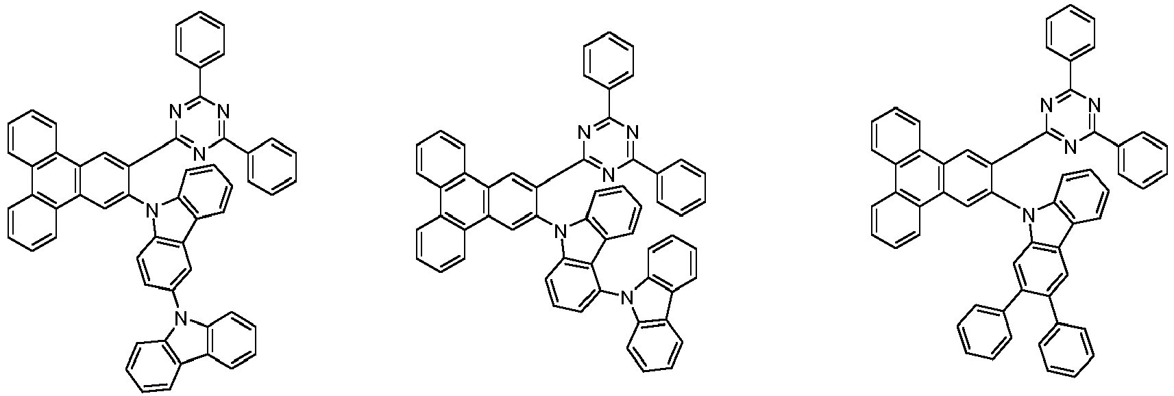


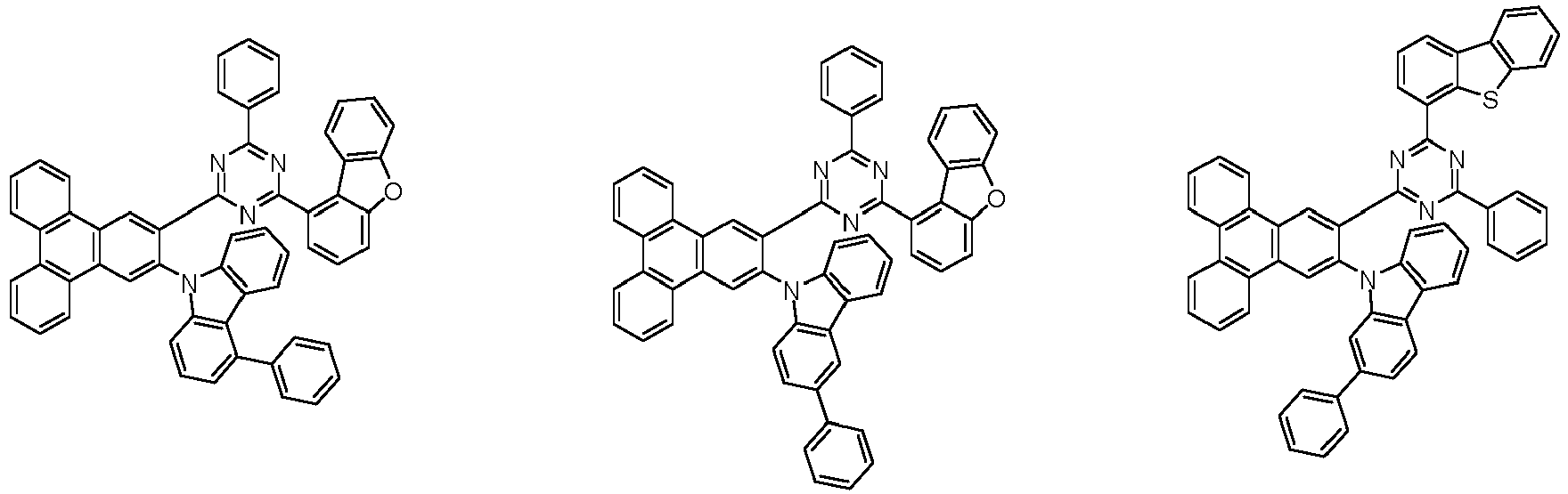


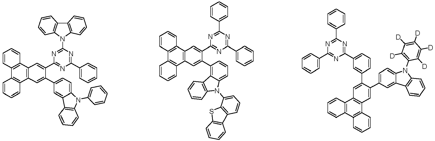


- Since the compound represented by
Chemical Formula 1 has a triphenylene structure, it is possible to exhibit excellent heat resistance. Because the carbazole-based group having hole transfer characteristics and the triazine-based group (pyridine, pyrimidine, and triazine) having electron transport characteristics are adjacent to each other in an ortho position, intra charge transfer can be easily performed. Therefore, the stability of the molecule is high, and it is advantageous for both hole and electron transport. In addition, various aryl groups and heterocycles are additionally substituted in Ar1 and Ar2 ofChemical Formula 1, so that electron transport properties can be variously controlled, which is advantageous for balancing charges according to changes in the common layer. - Therefore, the organic light emitting device using the same can have high efficiency, a low driving voltage, a long lifetime, and the like.
- The compound represented by
Chemical Formula 1 is prepared according to the preparation method as shown in Reaction Scheme A-1 and Reaction Scheme A-2.

- In Reaction Scheme A-1 and A-2, the remaining definitions excluding X are as defined above, and X is a halogen, for example bromo, chloro, or iodo.
- Reaction Scheme A-1 and A-2 are a Suzuki coupling reaction and an amine substitution reaction. These reactions are preferably carried out in the presence of a palladium catalyst and a base. The type of the reactive group and the catalyst used in the above reaction scheme can be appropriately changed. The above preparation method can be further specified in preparation examples described hereinafter.
- The present invention provides an organic light emitting device including the compound represented by
Chemical Formula 1. In one example, the present invention provides an organic light emitting device including: a first electrode; a second electrode provided at a side opposite to the first electrode; and at least one layer of organic material layers provided between the first electrode and the second electrode, wherein the at least one layer of the organic material layers includes a compound represented byChemical Formula 1. - The organic material layer of the organic light emitting device of the present invention may have a single layer structure, or it may have a multilayered structure in which two or more organic material layers are stacked. For example, the organic light emitting device of the present invention may have a structure including a hole injection layer, a hole transport layer, an electron inhibition layer, a light emitting layer, an electron transport layer, an electron injection layer, and the like as the organic material layer. However, the structure of the organic light emitting device is not limited thereto, and it may include a smaller number of organic layers.
- Further, the organic material layer may include a hole injection layer, a hole transport layer, or a layer simultaneously performing hole injection and transport, wherein the hole injection layer, the hole transport layer, and the layer simultaneously performing hole injection and transport include a compound represented by
Chemical Formula 1. - Further, The organic material layer may include an electron inhibition layer, wherein the electron inhibition layer includes a compound represented by
Chemical Formula 1. - Further, the organic material layer may include a light emitting layer, wherein the light emitting layer includes a compound represented by
Chemical Formula 1. - Further, the organic material layer may include an electron transport layer or an electron injection layer, or a layer simultaneously performing electron transport and injection, wherein the electron transport layer, the electron injection layer, and the layer simultaneously performing electron transport and injection include a compound represented by
Chemical Formula 1. - Further, the organic material layer may include a hole injection layer, a hole transport layer, an electron inhibition layer, and a light emitting layer, wherein any one or more selected from the group consisting of the hole injection layer, the hole transport layer, and the electron inhibition layer may include the compound represented by
Chemical Formula 1. - Further, the organic light emitting device according to the present invention may be a normal type of organic light emitting device in which an anode, one or more organic material layers, and a cathode are sequentially stacked on a substrate. Further, the organic light emitting device according to the present invention may be an inverted type of organic light emitting device in which a cathode, one or more organic material layers, and an anode are sequentially stacked on a substrate. For example, the structure of an organic light emitting device according to an embodiment of the present invention is illustrated in
FIGS. 1 and 2 . -
FIG. 1 shows an example of an organic light emitting device including asubstrate 1, ananode 2, alight emitting layer 3, and acathode 4. In such a structure, the compound represented byChemical Formula 1 may be included in the light emitting layer. -
FIG. 2 shows an example of an organic light emitting device including asubstrate 1, ananode 2, ahole injection layer 5, ahole transport layer 6, anelectron inhibition layer 7, alight emitting layer 3, anelectron transport layer 8, anelectron injection layer 9, and acathode 4. In such a structure, the compound represented byChemical Formula 1 may be included in one or more layers of the hole injection layer, the hole transport layer, the electron inhibition layer, the light emitting layer, the hole blocking layer, and the electron injection and transport layer. - The organic light emitting device according to the present invention may be manufactured by materials and methods known in the art, except that at least one layer of the organic material layers includes the compound represented by
Chemical Formula 1. In addition, when the organic light emitting device includes a plurality of organic material layers, the organic material layers may be formed of the same material or different materials. - For example, the organic light emitting device according to the present invention can be manufactured by sequentially stacking a first electrode, an organic material layer, and a second electrode on a substrate. In this case, the organic light emitting device may be manufactured by depositing a metal, metal oxides having conductivity, or an alloy thereof on the substrate to form the anode, forming a organic material layer including the hole injection layer, the hole transport layer, the light emitting layer, and the electron transport layer thereon, and then depositing a material that can be used as the cathode thereon, by using a PVD (physical vapor deposition) method such as a sputtering method or an e-beam evaporation method. In addition to such a method, the organic light emitting device may be manufactured by sequentially depositing a cathode material, an organic material layer, and an anode material on a substrate.
- In addition, the compound represented by
Chemical Formula 1 may be formed into an organic layer by a solution coating method as well as a vacuum deposition method at the time of manufacturing an organic light emitting device. Herein, the solution coating method means spin coating, dip coating, doctor blading, inkjet printing, screen printing, a spray method, roll coating, or the like, but is not limited thereto. - In addition to such a method, the organic light emitting device may be manufactured by sequentially depositing a cathode material, an organic material layer, and an anode material on a substrate (
International Publication WO 2003/012890 ). However, the manufacturing method is not limited thereto. - For example, the first electrode is an anode and the second electrode is a cathode, or the first electrode is a cathode and the second electrode is an anode.
- As the anode material, generally, a material having a large work function is preferably used so that holes can be smoothly injected into the organic material layer. Specific examples of the anode material include metals such as vanadium, chrome, copper, zinc, and gold, or an alloy thereof; metal oxides such as zinc oxides, indium oxides, indium tin oxides (ITO), and indium zinc oxides (IZO); a combination of metals and oxides, such as ZnO:Al or SnO2:Sb; conductive polymers such as poly(3-methylthiophene), poly[3,4-(ethylene-1,2-dioxy)thiophene] (PEDOT), polypyrrole, polyaniline, and the like, but are not limited thereto.
- As the cathode material, generally, a material having a small work function is preferably used so that electrons can be easily injected into the organic material layer. Specific examples of the cathode material include metals such as magnesium, calcium, sodium, potassium, titanium, indium, yttrium, lithium, gadolinium, aluminum, silver, tin, and lead, or an alloy thereof; and a multilayered structure material such as LiF/Al or LiO2/Al, and the like, but are not limited thereto.
- The hole injection layer is a layer for injecting holes from the electrode, and the hole injection material is preferably a compound which has a capability of transporting the holes, thus has a hole injecting effect in the anode and an excellent hole-injecting effect to the light emitting layer or the light emitting material, prevents excitons produced in the light emitting layer from moving to the electron injection layer or the electron injection material, and is excellent in the ability to form a thin film. It is preferable that a HOMO (highest occupied molecular orbital) of the hole injection material is between the work function of the anode material and a HOMO of a peripheral organic material layer. Specific examples of the hole injection material include metal porphyrin, oligothiophene, an arylamine-based organic material, a hexanitrilehexaazatriphenylene-based organic material, a quinacridone-based organic material, a perylene-based organic material, anthraquinone, a polyaniline and polythiophene-based conductive polymer, and the like, but are not limited thereto.
- The hole transport layer is a layer that receives holes from a hole injection layer and transports the holes to the light emitting layer. The hole transport material is suitably a material having large mobility to the holes, which may receive holes from the anode or the hole injection layer and transfer the holes to the light emitting layer. Specific examples thereof include an arylamine-based organic material, a conductive polymer, a block copolymer in which a conjugate portion and a non-conjugate portion are present together, and the like, but are not limited thereto.
- The electron inhibition layer is a layer provided between the hole transport layer and the light emitting layer in order to prevent the electrons injected from the cathode from being transferred to the hole transport layer without being recombined in the light emitting layer, which may also be referred to as an electron blocking layer. The electron inhibition layer is preferably a material having a smaller electron affinity than the electron transport layer.
- The light emitting material is preferably a material which may receive holes and electrons transported from a hole transport layer and an electron transport layer, respectively, and combine the holes and the electrons to emit light in a visible ray region, and has good quantum efficiency to fluorescence or phosphorescence. Specific examples of the light emitting material include an 8-hydroxy-quinoline aluminum complex (Alq3); a carbazole-based compound; a dimerized styryl compound; BAlq; a 10-hydroxybenzoquinoline-metal compound; a benzoxazole, benzothiazole, and benzimidazole-based compound; a poly(p-phenylenevinylene) (PPV)-based polymer; a spiro compound; polyfluorene; rubrene; and the like, but are not limited thereto.
- The light emitting layer may include a host material and a dopant material. The host material may be a fused aromatic ring derivative, a heterocycle-containing compound, or the like. Specific examples of the fused aromatic ring derivatives include anthracene derivatives, pyrene derivatives, naphthalene derivatives, pentacene derivatives, phenanthrene compounds, and fluoranthene compounds. Examples of heterocyclic compounds include carbazole derivatives, dibenzofuran derivatives, furan compounds, pyrimidine derivatives, and the like, but are not limited thereto.
- Examples of the dopant material include an aromatic amine derivative, a styrylamine compound, a boron complex, a fluoranthene compound, a metal complex, and the like. Specific examples of the aromatic amine derivatives include substituted or unsubstituted fused aromatic ring derivatives having an arylamino group, and examples thereof include pyrene, anthracene, chrysene, and periflanthene having the arylamino group, and the like, and the styrylamine compound is a compound where at least one arylvinyl group is substituted in substituted or unsubstituted arylamine. Specific examples thereof include styrylamine, styryldiamine, styryltriamine, styryltetramine, and the like, but are not limited thereto. Further, examples of the metal complex include an iridium complex, a platinum complex, and the like, but are not limited thereto.
- The electron transport layer is a layer which receives electrons from an electron injection layer and transports the electrons to a light emitting layer, and an electron transport material is suitably a material which may receive electrons well from a cathode and transfer the electrons to a light emitting layer, and has a large mobility for electrons. Specific examples thereof include: an Al complex of 8-hydroxyquinoline; a complex including Alq3; an organic radical compound; a hydroxyflavone-metal complex, and the like, but are not limited thereto. The electron transport layer may be used with any desired cathode material, as used according to the related art. In particular, appropriate examples of the cathode material are a typical material which has a low work function, followed by an aluminum layer or a silver layer. Specific examples thereof include cesium, barium, calcium, ytterbium, and samarium, in each case followed by an aluminum layer or a silver layer.
- The electron injection layer is a layer which injects electrons from an electrode, and is preferably a compound which has a capability of transporting electrons, has an effect of injecting electrons from a cathode and an excellent effect of injecting electrons into a light emitting layer or a light emitting material, prevents excitons produced from the light emitting layer from moving to a hole injection layer, and is also excellent in the ability to form a thin film. Specific examples thereof include fluorenone, anthraquinodimethane, diphenoquinone, thiopyran dioxide, oxazole, oxadiazole, triazole, imidazole, perylenetetracarboxylic acid, fluorenylidene methane, anthrone, and the like, and derivatives thereof, a metal complex compound, a nitrogen-containing 5-membered ring derivative, and the like, but are not limited thereto.
- Examples of the metal complex compound include 8-hydroxyquinolinato lithium, bis(8-hydroxyquinolinato)zinc, bis(8-hydroxyquinolinato)copper, bis(8-hydroxyquinolinato)manganese, tris(8-hydroxyquinolinato)aluminum, tris(2-methyl-8-hydroxyquinolinato)aluminum, tris(8-hydroxyquinolinato)gallium, bis(10-hydroxybenzo[h]quinolinato)beryllium, bis(10-hydroxybenzo[h]quinolinato)zinc, bis(2-methyl-8-quinolinato)chlorogallium, bis(2-methyl-8-quinolinato)(o-cresolato)gallium, bis(2-methyl-8-quinolinato)(1-naphtholato)aluminum, bis(2-methyl-8-quinolinato)(2-naphtholato)gallium, and the like, but are not limited thereto.
- The organic light emitting device according to the present invention may be a front side emission type, a back side emission type, or a double side emission type according to the used material.
- In addition, the compound represented by
Chemical Formula 1 may be included in an organic solar cell or an organic transistor in addition to an organic light emitting device. - The preparation of the compound represented by
Chemical Formula 1 and the organic light emitting device containing the same will be described in detail in the following examples. However, these examples are presented for illustrative purposes only, and are not intended to limit the scope of the present invention. -

- 4-Bromo-chloro-2-iodoaniline (50 g, 150.4 mmol) and [1,1'-biphenyl]-2-yl-boronic acid (29.8 g, 150.4 mmol)) were added in 1000 mL of tetrahydrofuran, and then stirred and refluxed under a nitrogen atmosphere. Then, sodium carbonate (47.8 g, 451.3 mmol) was dissolved in 48 ml of water, and the aqueous solution was added thereto, and then sufficiently stirred. Then, tetrakis(triphenylphosphine)palladium (5.2 g, 4.5 mmol) was added thereto. After two hours of reaction, the reaction mixture was cooled to room temperature. The reaction mixture was separated into an organic layer and an aqueous layer, and then the organic layer was distilled. This was dissolved in 1079 ml of chloroform 20 times, and washed two times with water, then the organic layer was separated, removed, and dried over anhydrous magnesium sulfate, and distilled under reduced pressure. The concentrated material was recrystallized using a mixed solution of chloroform and hexane to produce a brown solid Compound 1-a (43.2 g, 80 %, MS: [M+H]+ = 359.7).
-

- Compound 1-a (40 g, 111.5 mmol) was added in 700 mL of 2M hydrochloric acid, and then stirred for 15 minute at 0 °C, and then sodium nitrite (8.5 g, 122.6 mmol) slowly added thereto. After one hour, the mixture was heated at 60 °C for 3 hours, and then the mixture was cooled to room temperature. The reaction mixture was separated into an organic layer and an aqueous layer, and then the organic layer was distilled. This was dissolved in 800 ml of chloroform 20 times, and washed two times with water, then the organic layer was separated, removed, and dried over anhydrous magnesium sulfate, and distilled under reduced pressure. The concentrated material was recrystallized using a mixed solution of chloroform and hexane to produce a brown solid Compound 1-b (27.4 g, 72 %, MS: [M+H]+ = 342.0).
-

- Compound 1-b (25 g, 73.3 mmol) and bis(pinacolato)diboron (18.6 g, 73.3 mmol) were added in 500 mL of Diox, and then stirred and refluxed under a nitrogen atmosphere. Then, potassium phosphate tribasic (46.7 g, 219.9 mmol) was added thereto, and then sufficiently stirred. Then, dibenzylideneacetone palladium (1.3 g, 2.2 mmol) and tricyclohexylphosphine (1.2 g, 4.4 mmol) were added thereto. After three hours of reaction, the reaction mixture was cooled to room temperature and an organic layer was filtered to remove the base. The filtrated organic layer was distilled. This was dissolved in 285 ml of chloroform 10 times, and washed two times with water, then the organic layer was separated, removed, and dried over anhydrous magnesium sulfate, and distilled under reduced pressure. The concentrated material was recrystallized using a mixed solution of chloroform and hexane to produce a brown solid Compound 1-c (22.8 g, 80 %, MS: [M+H]+ = 389.7).
-
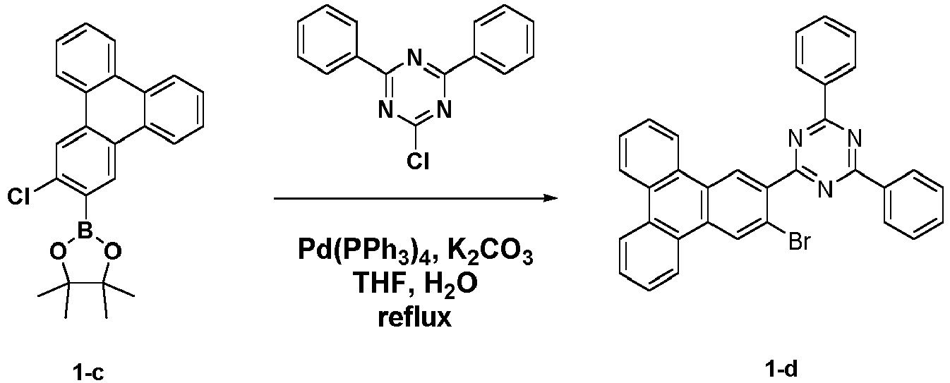
- Compound 1-c (20 g, 51.5 mmol) and 2-chloro-4,6-diphenyl-1,3,5-triazine (13.8 g, 51.5 mmol) were added to 400 mL of tetrahydrofuran, and then stirred and refluxed under a nitrogen atmosphere. Then, sodium carbonate (16.4 g, 154.4 mmol) was dissolved in 16 ml of water, and the aqueous solution was added thereto, and then sufficiently stirred. Then, tetrakis(triphenylphosphine)palladium (1.8 g, 1.5 mmol) was added thereto. After one hour of reaction, the reaction mixture was cooled to room temperature. The reaction mixture was separated into an organic layer and an aqueous layer, and then the organic layer was distilled. This was dissolved in 554 ml of chloroform 20 times, and washed two times with water, then the organic layer was separated, removed, and dried over anhydrous magnesium sulfate, and distilled under reduced pressure. The concentrated material was recrystallized using a mixed solution of chloroform and ethyl acetate to produce a yellow solid Compound 1-d (19.1 g, 69 %, MS: [M+H]+ = 539.5).
-

- Compound 1-d (18 g, 33.4 mmol) and 9H-carbazol (5.6 g, 33.4 mmol) were added to 360 mL of xylene, and then stirred and refluxed under a nitrogen atmosphere. Then, sodium tert-butoxide (9.6 g, 100.3 mmol) was added thereto, and then sufficiently stirred. Then, bis(tri-tert-butylphosphine)palladium (0.5 g, 1 mmol) was added thereto. After one hour of reaction, the reaction mixture was cooled to room temperature and an organic layer was filtered to remove the base. The filtrated organic layer was distilled. This was dissolved in 209 ml of chloroform 10 times, and washed two times with water, then the organic layer was separated, removed, and dried over anhydrous magnesium sulfate, and distilled under reduced pressure. The concentrated material was purified using a mixed solution of chloroform and ethyl acetate through a silica column to produce a yellow solid Compound 1 (13.2 g, 63 %, MS: [M+H]+ = 625.8).
-

- Compound 2 (MS: [M+H]+ = 633.8) was prepared in the same manner as in the preparation of
Compound 1, except that 9H-carbazole-1,2,3,4,5,6,7,8-d8 was used instead of 9H-carbazole in Preparation Example 1. -

- Compound 3 (MS: [M+H]+ = 725) was prepared in the same manner as in the preparation of
Compound 1, except that 2-chloro-4-(phenanthrene-9-yl)-6-phenyl-1,3,5-triazine was used instead of 2-chloro-4,6-diphenyl-1,3,5-triazine in Preparation Example 1. -

- Compound 4 (MS: [M+H]+ = 701) was prepared in the same manner as in the preparation of
Compound 1, except that 2-(3-chlorophenyl)-4,6-diphenyl-1,3,5-triazine was used instead of 2-chloro-4,6-diphenyl-1,3,5-triazine in Preparation Example 1. -
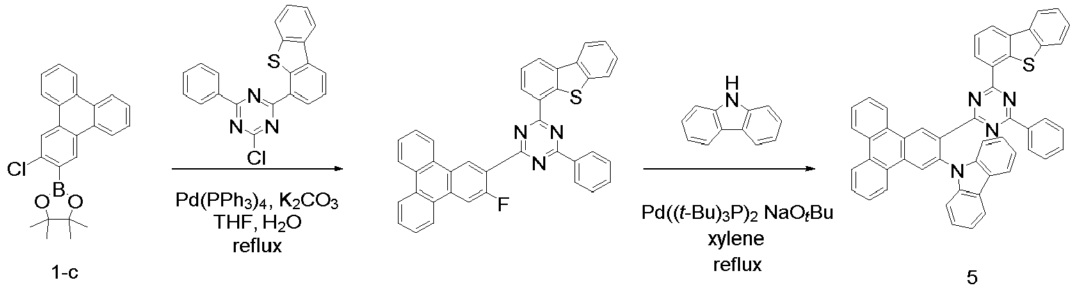
- Compound 5 (MS: [M+H]+ = 731) was prepared in the same manner as in the preparation of
Compound 1, except that 2-chloro-4-(dibenzo[b,d]thiophene-4-yl)-6-phenyl-1,3,5-trizine was used instead of 2-chloro-4,6-diphenyl-1,3,5-triazine in Preparation Example 1. -

- Compound 6 (MS: [M+H]+ = 722) was prepared in the same manner as in the preparation of
Compound 1, except that 9H-carbazole-1,2,3,4,5,6,7,8-d8 was used instead of 9H-carbazole and 9-(4-chloro-6-phenyl-1,3,5-triazin-2-yl)-9H-carbazole was used instead of 2-chloro-4,6-diphenyl-1,3,5-triazine in Preparation Example 1. -

- Compound 7-d (MS: [M+H]+ = 543) was prepared in the same manner as in the preparation of Compound 1-d, except that 2-chloro-4-phenyl-6-(phenyl-d5)-1,3,5-triazine was used instead of 2-chloro-4,6-diphenyl-1,3,5-triazine in Preparation Example 1.
-

- Compound 7-d (15 g, 27.6 mmol) and (9-phenyl-9H-carbazol-3-yl)boronic acid (7.9 g, 27.6 mmol) were added to 300 mL of tetrahydrofuran, and then stirred and refluxed under a nitrogen atmosphere. Then, sodium carbonate (8.8 g, 82.8 mmol) was dissolved in 9 ml of water, and the aqueous solution was added thereto, and then sufficiently stirred. Then, tetrakis(triphenylphosphine)palladium (1 g, 0.8 mmol) was added thereto. After one hour of reaction, the reaction mixture was cooled to room temperature and an organic layer was filtered. This was dissolved in 390 ml of chloroform20 times, and washed two times with water, then the organic layer was separated, removed, and dried over anhydrous magnesium sulfate, and distilled under reduced pressure. The concentrated material was recrystallized using a mixed solution of chloroform and ethyl acetate to produce a white solid Compound 7 (10.9 g, 56 %, MS: [M+H]+ = 706.9).
-

- Compound 8 (MS: [M+H]+ = 791) was prepared in the same manner as in the preparation of
Compound 7, except that 2-chloro-4-(dibenzo[b,d]furane-3-yl)-6-phenyl-1,3,5-trizine was used instead of 2-chloro-4-phenyl-6-(phenyl-d5)-1,3,5-triazine in Preparation Example 7. - A glass substrate on which a thin film of ITO (indium tin oxide) was coated at a thickness of 1400 Å was put into distilled water containing a detergent dissolved therein and washed by ultrasonic waves. In this case, the detergent used was a product commercially available from Fisher Co., and the distilled water was one which had been filtered twice by using a filter that is commercially available from Millipore Co. The ITO was washed for 30 minutes, and ultrasonic washing was then repeated twice for 10 minutes by using distilled water. After the washing with distilled water was completed, the substrate was ultrasonically washed with a solvent of isopropyl alcohol, acetone, and methanol, and dried, after which it was transported to a plasma cleaner. Then, the substrate was cleaned with oxygen plasma for 5 minutes, and then transferred to a vacuum evaporator.
- On the ITO transparent electrode thus prepared, the following compound HT-A and the following compound PD were thermally vacuum deposited at a ratio of 95:5 (molar ratio) to have a thickness of 100 Å, and then only the following compound HT-A was thermally vacuum deposited to have a thickness of 1150 Å, thereby forming a hole transport layer. The following compound HT-B was thermally vacuum-deposited on the hole transport layer to a thickness of 450 Å to form a electron inhibition (blocking) layer. Then, on the electron
inhibition layer Compound 1 prepared above and the following compound GD were thermally vacuum deposited at a ratio of 85:15 (molar ratio) to have a thickness of 400 Å, thereby forming a light-emitting layer. On the light-emitting layer, the following compound ET-A was thermally vacuum deposited to have a thickness of 50 Å, thereby forming a hole blocking layer. Then, on a hole blocking layer the following compound ET-B and the following compound Liq were thermally vacuum deposited at a ratio of 2:1 (weight ratio) to have a thickness of 250 Å, and then LiF and magnesium were thermally vacuum deposited at a ratio of 1:1 (weight ratio) to have a thickness of 30 Å, thereby forming an electron transport and injection layer. On the electron injection layer, magnesium and silver were thermally vacuum deposited at a ratio of 1: 4 (weight ratio) to have a thickness of 160 Å, thereby forming a cathode. The organic light emitting device was manufactured.

- In the above process, the vapor deposition rate of the organic material was maintained at 0.4 to 0.7 Å/s, the lithium fluoride was deposited at 0.3 Å/s, the silver and magnesium were deposited at 2 Å/s, and the degree of vacuum during vapor deposition was maintained at 2×10⁻⁷ ∼ 5×10⁻⁶ torr. The organic light emitting device was manufactured.
- The organic light emitting device was manufactured in the same manner as in Example 1, except that the compounds shown in Table 1 below was used instead of the
compound 1. - For reference, in Examples 9 and 10 and Comparative Examples 3 and 4, an organic light emitting device was manufactured by using the compound shown in Table 1 below in a weight ratio of 1:1 instead of
Compound 1. Taking Example 8 as an example, instead ofCompound 1 in Example 1,Compound 1 and Compound H-2 were used in a weight ratio of 1:1. In Table 1, compounds H-2, C1, and C2 are as follows.
- The driving voltage, efficiency, and lifetime were measured for the organic light emitting devices manufactured in the examples and comparative examples above, and the results are shown in Table 1 below. The driving voltage and efficiency were measured at a current density of 10 mA/cm2. Further, in Table 1 below, T95 means the time required for the luminance to be reduced to 95 % of the initial luminance at a current density of 20 mA/cm2.
[Table 1] Category Light emitting layer compound Voltage (V) (@10 mA/cm2) Efficiency(cd/A) (@10 mA/cm2) Emission color T95 (@20 mA/cm2) Example 1 Compound 13.01 65.9 green 77 Example 2 Compound 23.00 65.8 green 87 Example 3 Compound 33.06 66.6 green 75 Example 4 Compound 42.97 67.2 green 72 Example 5 Compound 53.00 66.3 green 76 Example 6 Compound 63.06 66.1 green 99 Example 7 Compound 73.02 65.0 green 70 Example 8 Compound 82.98 65.9 green 75 Example 9 Compound 1, Compound H-23.11 70.0 green 85 Example 10 Compound 8, Compound H-23.17 72.5 green 80 Comparative Example 1 Compound C1 3.05 67.1 green 60 Comparative Example 2 Compound C2 3.06 66.0 green 57 Comparative Example 3 Compound C1, Compound H-2 3.12 78.5 green 76 Comparative Example 4 Compound C2, Compound H-2 3.20 79.2 green 70 - Examples 1 to 8 and Comparative Examples 1 and 2 were device examples using a single host in the light emitting layer. Since the carbazole-based group having hole transfer characteristics and the triazine-based group (pyridine, pyrimidine, and triazine) having electron transport characteristics are adjacent to each other in an ortho position, intra charge transfer can be easily performed. Therefore, the stability of the molecule is high, and it is advantageous for both hole and electron transport. In addition, various aryl groups and heterocycles are additionally substituted in Ar1 and Ar2 of
Chemical Formula 1, so that electron transport properties can be variously controlled, which is advantageous for balancing charges according to changes in the common layer. - Examples 9 and 10 are device examples using two types of hosts in the light emitting layer. Even when two types of hosts are used in the light emitting layer, it can be seen that the devices of Examples 9 and 10 using the compounds of the present invention have higher efficiencies than the devices of Comparative Examples 3 and 4, and in particular, have significantly improved life characteristics.
- Therefore, as shown in Table 1, when the compound of
Chemical Formula 1 is used as a host for an organic light emitting device, it can be seen that characteristics of low voltage, high efficiency, and long life appear. -
1: substrate 2: anode 3: light emitting layer 4: cathode 5: hole injection layer 6: hole transport layer 7: electron inhibition layer 8: electron transport layer 9: electron injection layer
Claims (10)
- A compound represented by the following Chemical Formula 1:

L is a direct bond, or a substituted or unsubstituted C6-60 arylene,
A is a substituted or unsubstituted carbazolyl,
X1, X2, and X3 are each independently N or CH, with the proviso that at least one of X1, X2, and X3 is N, and
Ar1 and Ar2 are each independently a substituted or unsubstituted C6-60 aryl, or a substituted or unsubstituted C5-60 heteroaryl containing at least one of heteroatom selected from the group consisting of N, O, and S. - The compound of claim 1,
wherein the compound represented by Chemical Formula 1 is the compounds represented by the following Chemical Formulas 2 or 3: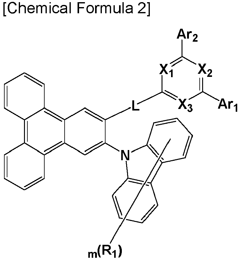

L, X1, X2, X3, Ar1, and Ar2 are as defined in Claim 1,
R1 are each independently hydrogen, deuterium, a substituted or unsubstituted C1-60 alkyl, a substituted or unsubstituted C6-60 aryl, or a substituted or unsubstituted C5-60 heteroaryl containing at least one of N, O, and S,
R2 is a substituted or unsubstituted C1-60 alkyl, or a substituted or unsubstituted C6-60 aryl,
R3 are each independently hydrogen, deuterium, a substituted or unsubstituted C1-60 alkyl, a substituted or unsubstituted C6-60 aryl, or a substituted or unsubstituted C5-60 heteroaryl containing at least one of N, O, and S,
m is an integer of 0 to 8, and
n is an integer of 0 to 7. - The compound of claim 1,
wherein all of X1, X2, and X3 are N. - The compound of claim 1,
wherein L is a direct bond, phenylene, or biphenylylene, and
the phenylene or biphenylylene are each independently substituted by at least one deuterium or not. - The compound of claim 1,
wherein Ar1 and Ar2 are each independently phenyl, biphenylyl, terphenylyl, dimethylfluorenyl, naphthyl, phenanthrenyl, triphenylenyl, dibenzofuranyl, dibenzothiophenyl, carbazol-9-yl, 9-phenyl-9H-carbazolyl, benzoxazolyl, benzothiazolyl, 2-phenylbenzoxazolyl, or 2-phenyl benzothiazolyl,
which are each independently substituted by at least one deuterium or not. - The compound of claim 2,
wherein R1 are each independently hydrogen, deuterium, phenyl, dibenzofuranyl, dibenzothiophenyl, or carbazolyl,
and the phenyl, dibenzofuranyl, dibenzothiophenyl, and carbazolyl are each independently substituted by at least one deuterium or not. - The compound of claim 2,
wherein R2 are each independently phenyl substituted by at least one deuterium or not. - The compound of claim 2,
wherein R3 are each independently hydrogen, deuterium, phenyl, dibenzofuranyl, dibenzothiophenyl, or carbazolyl, and
the phenyl, dibenzofuranyl, dibenzothiophenyl, or carbazolyl are each independently substituted by at least one deuterium or not. - The compound of claim 1,
wherein the compound represented by Chemical Formula 1 is any one selected from the group consisting of the following formulas:


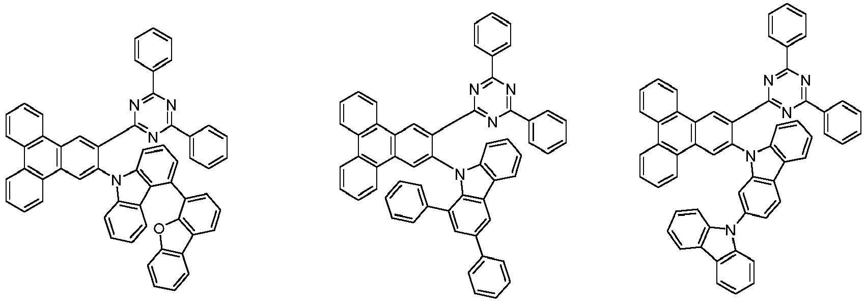


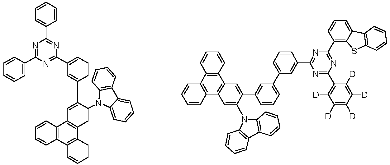


- An organic light emitting device comprising: a first electrode; a second electrode provided at a side opposite to the first electrode; and at least one layer of the organic material layers provided between the first electrode and the second electrode, wherein the at least one layer of the organic material layer includes the compound according to any one of claims 1 to 9.
Applications Claiming Priority (3)
| Application Number | Priority Date | Filing Date | Title |
|---|---|---|---|
| KR20190029507 | 2019-03-14 | ||
| KR1020200030982A KR102456677B1 (en) | 2019-03-14 | 2020-03-12 | Novel compound and organic light emitting device comprising the same |
| PCT/KR2020/003542 WO2020185038A1 (en) | 2019-03-14 | 2020-03-13 | Novel compound and organic light emitting device using same |
Publications (3)
| Publication Number | Publication Date |
|---|---|
| EP3862350A4 EP3862350A4 (en) | 2021-08-11 |
| EP3862350A1 true EP3862350A1 (en) | 2021-08-11 |
| EP3862350B1 EP3862350B1 (en) | 2024-06-12 |
Family
ID=72708207
Family Applications (1)
| Application Number | Title | Priority Date | Filing Date |
|---|---|---|---|
| EP20769606.3A Active EP3862350B1 (en) | 2019-03-14 | 2020-03-13 | Novel compound and organic light emitting device using same |
Country Status (6)
| Country | Link |
|---|---|
| US (1) | US11910711B2 (en) |
| EP (1) | EP3862350B1 (en) |
| JP (1) | JP7187752B2 (en) |
| KR (1) | KR102456677B1 (en) |
| CN (1) | CN112888683B (en) |
| TW (1) | TWI717232B (en) |
Families Citing this family (11)
| Publication number | Priority date | Publication date | Assignee | Title |
|---|---|---|---|---|
| KR102907314B1 (en) * | 2021-02-26 | 2026-01-02 | 주식회사 엘지화학 | Organic light emitting device |
| US20240114770A1 (en) * | 2021-02-26 | 2024-04-04 | Lg Chem, Ltd. | Organic light emitting device |
| KR102822388B1 (en) * | 2021-03-19 | 2025-06-20 | 삼성에스디아이 주식회사 | Composition for organic optoelectronic device, organic optoelectronic device and display device |
| KR102807136B1 (en) * | 2021-09-03 | 2025-05-16 | 삼성에스디아이 주식회사 | Composition for optoelectronic device and organic optoelectronic device and display device |
| US20240164205A1 (en) * | 2021-09-03 | 2024-05-16 | Samsung Sdi Co., Ltd. | Composition for organic optoelectronic device, organic optoelectronic device, and display device |
| WO2023055177A1 (en) * | 2021-10-01 | 2023-04-06 | 주식회사 엘지화학 | Novel compound and organic light-emitting device comprising same |
| WO2023153795A1 (en) * | 2022-02-08 | 2023-08-17 | 주식회사 엘지화학 | Novel compound and organic light-emitting device comprising same |
| KR20240131122A (en) * | 2023-02-23 | 2024-08-30 | 삼성에스디아이 주식회사 | Compound for organic optoelectronic device, organic optoelectronic device and display device |
| CN119384416A (en) * | 2023-03-17 | 2025-01-28 | 株式会社Lg化学 | New compound and organic light-emitting device containing the same |
| KR20250058805A (en) * | 2023-10-23 | 2025-05-02 | 엘티소재주식회사 | Compound, organic light emitting device comprising same and composition for organic material layer |
| WO2026017611A1 (en) | 2024-07-15 | 2026-01-22 | Merck Patent Gmbh | Organic light emitting device |
Family Cites Families (26)
| Publication number | Priority date | Publication date | Assignee | Title |
|---|---|---|---|---|
| DE10135513B4 (en) | 2001-07-20 | 2005-02-24 | Novaled Gmbh | Light-emitting component with organic layers |
| JP4336537B2 (en) * | 2003-07-31 | 2009-09-30 | キヤノン株式会社 | Organic light emitting device |
| US20100084967A1 (en) | 2007-03-28 | 2010-04-08 | Fujifilm Corporation | Organic electroluminescent device |
| KR20090132350A (en) * | 2008-06-20 | 2009-12-30 | 손석환 | Image transformer integrated terminal block |
| KR101235369B1 (en) | 2010-01-21 | 2013-02-20 | (주)씨에스엘쏠라 | Organic light emitting compound and organic light emitting device comprising the same |
| KR101497133B1 (en) | 2011-12-23 | 2015-02-27 | 제일모직 주식회사 | Compound for organic OPTOELECTRONIC device, ORGANIC LIGHT EMITTING DIODE INCLUDING THE SAME and DISPLAY INCLUDING THE organic LIGHT EMITTING DIODE |
| US9705099B2 (en) | 2012-01-26 | 2017-07-11 | Universal Display Corporation | Phosphorescent organic light emitting devices having a hole transporting cohost material in the emissive region |
| EP2875019B1 (en) | 2012-07-23 | 2017-03-29 | Merck Patent GmbH | Materials for organic electroluminescence devices |
| KR101649683B1 (en) | 2013-09-06 | 2016-08-19 | 제일모직 주식회사 | Composition for organic optoelectric device and organic optoelectric device and display device |
| KR20150085772A (en) * | 2014-01-16 | 2015-07-24 | 삼성디스플레이 주식회사 | Organic light-emitting device |
| CN104795503B (en) * | 2014-01-16 | 2018-07-20 | 三星显示有限公司 | Organic light emitting apparatus |
| KR102280686B1 (en) | 2014-02-11 | 2021-07-22 | 삼성전자주식회사 | Carbazole-based compound and organic light emitting device including the same |
| KR102326623B1 (en) | 2014-03-18 | 2021-11-16 | 메르크 파텐트 게엠베하 | Organic electroluminescent device |
| KR20160007967A (en) | 2014-07-10 | 2016-01-21 | 삼성디스플레이 주식회사 | Organic light emitting device |
| US10741772B2 (en) | 2014-08-29 | 2020-08-11 | Samsung Electronics Co., Ltd. | Organic light-emitting device |
| KR101694487B1 (en) * | 2014-10-24 | 2017-01-11 | (주)위델소재 | Quinoxaline derivative compound, pyridopyrazine derivative compound and organic electroluminescent devices using the sames |
| KR102490887B1 (en) * | 2015-09-11 | 2023-01-25 | 삼성디스플레이 주식회사 | Organic light emitting device |
| JP2019023163A (en) | 2015-10-21 | 2019-02-14 | 出光興産株式会社 | Novel compound, material for organic electroluminescent element, organic electroluminescent element, and electronic apparatus |
| CN108349914B9 (en) | 2015-10-27 | 2021-09-03 | 株式会社Lg化学 | Organic light emitting device |
| KR20170070359A (en) * | 2015-12-11 | 2017-06-22 | 삼성디스플레이 주식회사 | Organic light emitting device |
| TWI665286B (en) | 2016-07-27 | 2019-07-11 | 南韓商Lg化學股份有限公司 | Polycyclic compound and organic light emitting device including the same |
| WO2018074881A1 (en) | 2016-10-20 | 2018-04-26 | 주식회사 엘지화학 | Polycyclic compound and organic light emitting element comprising same |
| KR102643057B1 (en) | 2016-10-26 | 2024-03-04 | 솔루스첨단소재 주식회사 | Organic light-emitting compound and organic electroluminescent device using the same |
| TWI756292B (en) * | 2016-11-14 | 2022-03-01 | 德商麥克專利有限公司 | Compounds having an acceptor group and a donor group |
| WO2019176605A1 (en) | 2018-03-16 | 2019-09-19 | 日鉄ケミカル&マテリアル株式会社 | Organic electroluminescent element |
| KR102290362B1 (en) | 2018-06-19 | 2021-08-19 | 엘티소재주식회사 | Heterocyclic compound, organic light emitting device comprising the same, manufacturing method of the same and composition for organic layer of organic light emitting device |
-
2020
- 2020-03-12 KR KR1020200030982A patent/KR102456677B1/en active Active
- 2020-03-13 EP EP20769606.3A patent/EP3862350B1/en active Active
- 2020-03-13 TW TW109108452A patent/TWI717232B/en active
- 2020-03-13 US US17/285,179 patent/US11910711B2/en active Active
- 2020-03-13 JP JP2021520611A patent/JP7187752B2/en active Active
- 2020-03-13 CN CN202080005761.XA patent/CN112888683B/en active Active
Also Published As
| Publication number | Publication date |
|---|---|
| KR20200110226A (en) | 2020-09-23 |
| KR102456677B1 (en) | 2022-10-19 |
| US20210391544A1 (en) | 2021-12-16 |
| CN112888683B (en) | 2024-04-16 |
| CN112888683A (en) | 2021-06-01 |
| JP7187752B2 (en) | 2022-12-13 |
| EP3862350A4 (en) | 2021-08-11 |
| JP2022504972A (en) | 2022-01-13 |
| EP3862350B1 (en) | 2024-06-12 |
| US11910711B2 (en) | 2024-02-20 |
| TWI717232B (en) | 2021-01-21 |
| TW202039469A (en) | 2020-11-01 |
Similar Documents
| Publication | Publication Date | Title |
|---|---|---|
| CN112771033B (en) | Novel compound and organic light emitting device comprising the same | |
| EP3862350B1 (en) | Novel compound and organic light emitting device using same | |
| EP3862355A1 (en) | Novel compound and organic light emitting device comprising the same | |
| KR102562354B1 (en) | Novel compound and organic light emitting device comprising the same | |
| KR20210001936A (en) | Novel compound and organic light emitting device comprising the same | |
| EP3730488B1 (en) | Novel heterocyclic compound and organic light emitting device using same | |
| KR102889048B1 (en) | Novel compound and organic light emitting device comprising the same | |
| KR20200057651A (en) | Novel compound and organic light emitting device comprising the same | |
| KR102592082B1 (en) | Novel compound and organic light emitting device comprising the same | |
| KR102354501B1 (en) | Novel compound and organic light emitting device comprising the same | |
| KR102592081B1 (en) | Novel compound and organic light emitting device comprising the same | |
| EP4289836A1 (en) | Novel compound and organic light-emitting device comprising same | |
| KR102608810B1 (en) | Novel compound and organic light emitting device comprising the same | |
| EP3747873B1 (en) | Novel compound and organic light emitting diode using same | |
| KR20240122330A (en) | Novel compound and organic light emitting device comprising the same | |
| KR20200069247A (en) | Novel compound and organic light emitting device comprising the same | |
| KR102534717B1 (en) | Novel compound and organic light emitting device comprising the same | |
| KR20220037945A (en) | Novel compound and organic light emitting device comprising the same | |
| EP4299574B1 (en) | Novel compound and organic light-emitting device comprising same | |
| KR102909960B1 (en) | Organic light emitting device | |
| EP4345099A1 (en) | Novel compound and organic light-emitting device comprising same | |
| KR20200088172A (en) | Novel compound and organic light emitting device comprising the same |
Legal Events
| Date | Code | Title | Description |
|---|---|---|---|
| STAA | Information on the status of an ep patent application or granted ep patent |
Free format text: STATUS: THE INTERNATIONAL PUBLICATION HAS BEEN MADE |
|
| PUAI | Public reference made under article 153(3) epc to a published international application that has entered the european phase |
Free format text: ORIGINAL CODE: 0009012 |
|
| STAA | Information on the status of an ep patent application or granted ep patent |
Free format text: STATUS: REQUEST FOR EXAMINATION WAS MADE |
|
| 17P | Request for examination filed |
Effective date: 20210504 |
|
| A4 | Supplementary search report drawn up and despatched |
Effective date: 20210705 |
|
| AK | Designated contracting states |
Kind code of ref document: A1 Designated state(s): AL AT BE BG CH CY CZ DE DK EE ES FI FR GB GR HR HU IE IS IT LI LT LU LV MC MK MT NL NO PL PT RO RS SE SI SK SM TR |
|
| DAV | Request for validation of the european patent (deleted) | ||
| DAX | Request for extension of the european patent (deleted) | ||
| STAA | Information on the status of an ep patent application or granted ep patent |
Free format text: STATUS: EXAMINATION IS IN PROGRESS |
|
| 17Q | First examination report despatched |
Effective date: 20230315 |
|
| REG | Reference to a national code |
Ref country code: DE Ref legal event code: R079 Free format text: PREVIOUS MAIN CLASS: C07D0403040000 Ipc: C07D0405140000 Ref document number: 602020032357 Country of ref document: DE |
|
| GRAP | Despatch of communication of intention to grant a patent |
Free format text: ORIGINAL CODE: EPIDOSNIGR1 |
|
| STAA | Information on the status of an ep patent application or granted ep patent |
Free format text: STATUS: GRANT OF PATENT IS INTENDED |
|
| RIC1 | Information provided on ipc code assigned before grant |
Ipc: H10K 50/11 20230101ALI20240229BHEP Ipc: C07D 417/14 20060101ALI20240229BHEP Ipc: C07D 413/14 20060101ALI20240229BHEP Ipc: C07D 409/14 20060101ALI20240229BHEP Ipc: C07D 405/06 20060101ALI20240229BHEP Ipc: C07D 403/14 20060101ALI20240229BHEP Ipc: C07D 403/10 20060101ALI20240229BHEP Ipc: C07D 211/76 20060101ALI20240229BHEP Ipc: C07D 207/26 20060101ALI20240229BHEP Ipc: C07D 405/14 20060101AFI20240229BHEP |
|
| INTG | Intention to grant announced |
Effective date: 20240320 |
|
| GRAS | Grant fee paid |
Free format text: ORIGINAL CODE: EPIDOSNIGR3 |
|
| GRAA | (expected) grant |
Free format text: ORIGINAL CODE: 0009210 |
|
| STAA | Information on the status of an ep patent application or granted ep patent |
Free format text: STATUS: THE PATENT HAS BEEN GRANTED |
|
| AK | Designated contracting states |
Kind code of ref document: B1 Designated state(s): AL AT BE BG CH CY CZ DE DK EE ES FI FR GB GR HR HU IE IS IT LI LT LU LV MC MK MT NL NO PL PT RO RS SE SI SK SM TR |
|
| REG | Reference to a national code |
Ref country code: GB Ref legal event code: FG4D |
|
| REG | Reference to a national code |
Ref country code: CH Ref legal event code: EP |
|
| REG | Reference to a national code |
Ref country code: DE Ref legal event code: R096 Ref document number: 602020032357 Country of ref document: DE |
|
| REG | Reference to a national code |
Ref country code: IE Ref legal event code: FG4D |
|
| PG25 | Lapsed in a contracting state [announced via postgrant information from national office to epo] |
Ref country code: BG Free format text: LAPSE BECAUSE OF FAILURE TO SUBMIT A TRANSLATION OF THE DESCRIPTION OR TO PAY THE FEE WITHIN THE PRESCRIBED TIME-LIMIT Effective date: 20240612 |
|
| PG25 | Lapsed in a contracting state [announced via postgrant information from national office to epo] |
Ref country code: FI Free format text: LAPSE BECAUSE OF FAILURE TO SUBMIT A TRANSLATION OF THE DESCRIPTION OR TO PAY THE FEE WITHIN THE PRESCRIBED TIME-LIMIT Effective date: 20240612 Ref country code: HR Free format text: LAPSE BECAUSE OF FAILURE TO SUBMIT A TRANSLATION OF THE DESCRIPTION OR TO PAY THE FEE WITHIN THE PRESCRIBED TIME-LIMIT Effective date: 20240612 |
|
| REG | Reference to a national code |
Ref country code: LT Ref legal event code: MG9D |
|
| PG25 | Lapsed in a contracting state [announced via postgrant information from national office to epo] |
Ref country code: GR Free format text: LAPSE BECAUSE OF FAILURE TO SUBMIT A TRANSLATION OF THE DESCRIPTION OR TO PAY THE FEE WITHIN THE PRESCRIBED TIME-LIMIT Effective date: 20240913 |
|
| REG | Reference to a national code |
Ref country code: NL Ref legal event code: MP Effective date: 20240612 |
|
| PG25 | Lapsed in a contracting state [announced via postgrant information from national office to epo] |
Ref country code: ES Free format text: LAPSE BECAUSE OF FAILURE TO SUBMIT A TRANSLATION OF THE DESCRIPTION OR TO PAY THE FEE WITHIN THE PRESCRIBED TIME-LIMIT Effective date: 20240612 |
|
| PG25 | Lapsed in a contracting state [announced via postgrant information from national office to epo] |
Ref country code: LV Free format text: LAPSE BECAUSE OF FAILURE TO SUBMIT A TRANSLATION OF THE DESCRIPTION OR TO PAY THE FEE WITHIN THE PRESCRIBED TIME-LIMIT Effective date: 20240612 |
|
| PG25 | Lapsed in a contracting state [announced via postgrant information from national office to epo] |
Ref country code: NO Free format text: LAPSE BECAUSE OF FAILURE TO SUBMIT A TRANSLATION OF THE DESCRIPTION OR TO PAY THE FEE WITHIN THE PRESCRIBED TIME-LIMIT Effective date: 20240912 Ref country code: LV Free format text: LAPSE BECAUSE OF FAILURE TO SUBMIT A TRANSLATION OF THE DESCRIPTION OR TO PAY THE FEE WITHIN THE PRESCRIBED TIME-LIMIT Effective date: 20240612 Ref country code: HR Free format text: LAPSE BECAUSE OF FAILURE TO SUBMIT A TRANSLATION OF THE DESCRIPTION OR TO PAY THE FEE WITHIN THE PRESCRIBED TIME-LIMIT Effective date: 20240612 Ref country code: GR Free format text: LAPSE BECAUSE OF FAILURE TO SUBMIT A TRANSLATION OF THE DESCRIPTION OR TO PAY THE FEE WITHIN THE PRESCRIBED TIME-LIMIT Effective date: 20240913 Ref country code: FI Free format text: LAPSE BECAUSE OF FAILURE TO SUBMIT A TRANSLATION OF THE DESCRIPTION OR TO PAY THE FEE WITHIN THE PRESCRIBED TIME-LIMIT Effective date: 20240612 Ref country code: ES Free format text: LAPSE BECAUSE OF FAILURE TO SUBMIT A TRANSLATION OF THE DESCRIPTION OR TO PAY THE FEE WITHIN THE PRESCRIBED TIME-LIMIT Effective date: 20240612 Ref country code: BG Free format text: LAPSE BECAUSE OF FAILURE TO SUBMIT A TRANSLATION OF THE DESCRIPTION OR TO PAY THE FEE WITHIN THE PRESCRIBED TIME-LIMIT Effective date: 20240612 Ref country code: RS Free format text: LAPSE BECAUSE OF FAILURE TO SUBMIT A TRANSLATION OF THE DESCRIPTION OR TO PAY THE FEE WITHIN THE PRESCRIBED TIME-LIMIT Effective date: 20240912 |
|
| PG25 | Lapsed in a contracting state [announced via postgrant information from national office to epo] |
Ref country code: NL Free format text: LAPSE BECAUSE OF FAILURE TO SUBMIT A TRANSLATION OF THE DESCRIPTION OR TO PAY THE FEE WITHIN THE PRESCRIBED TIME-LIMIT Effective date: 20240612 |
|
| REG | Reference to a national code |
Ref country code: AT Ref legal event code: MK05 Ref document number: 1694152 Country of ref document: AT Kind code of ref document: T Effective date: 20240612 |
|
| PG25 | Lapsed in a contracting state [announced via postgrant information from national office to epo] |
Ref country code: NL Free format text: LAPSE BECAUSE OF FAILURE TO SUBMIT A TRANSLATION OF THE DESCRIPTION OR TO PAY THE FEE WITHIN THE PRESCRIBED TIME-LIMIT Effective date: 20240612 |
|
| PG25 | Lapsed in a contracting state [announced via postgrant information from national office to epo] |
Ref country code: PT Free format text: LAPSE BECAUSE OF FAILURE TO SUBMIT A TRANSLATION OF THE DESCRIPTION OR TO PAY THE FEE WITHIN THE PRESCRIBED TIME-LIMIT Effective date: 20241014 |
|
| PG25 | Lapsed in a contracting state [announced via postgrant information from national office to epo] |
Ref country code: PT Free format text: LAPSE BECAUSE OF FAILURE TO SUBMIT A TRANSLATION OF THE DESCRIPTION OR TO PAY THE FEE WITHIN THE PRESCRIBED TIME-LIMIT Effective date: 20241014 |
|
| PG25 | Lapsed in a contracting state [announced via postgrant information from national office to epo] |
Ref country code: PL Free format text: LAPSE BECAUSE OF FAILURE TO SUBMIT A TRANSLATION OF THE DESCRIPTION OR TO PAY THE FEE WITHIN THE PRESCRIBED TIME-LIMIT Effective date: 20240612 |
|
| PG25 | Lapsed in a contracting state [announced via postgrant information from national office to epo] |
Ref country code: EE Free format text: LAPSE BECAUSE OF FAILURE TO SUBMIT A TRANSLATION OF THE DESCRIPTION OR TO PAY THE FEE WITHIN THE PRESCRIBED TIME-LIMIT Effective date: 20240612 |
|
| PG25 | Lapsed in a contracting state [announced via postgrant information from national office to epo] |
Ref country code: AT Free format text: LAPSE BECAUSE OF FAILURE TO SUBMIT A TRANSLATION OF THE DESCRIPTION OR TO PAY THE FEE WITHIN THE PRESCRIBED TIME-LIMIT Effective date: 20240612 Ref country code: IS Free format text: LAPSE BECAUSE OF FAILURE TO SUBMIT A TRANSLATION OF THE DESCRIPTION OR TO PAY THE FEE WITHIN THE PRESCRIBED TIME-LIMIT Effective date: 20241012 |
|
| PG25 | Lapsed in a contracting state [announced via postgrant information from national office to epo] |
Ref country code: CZ Free format text: LAPSE BECAUSE OF FAILURE TO SUBMIT A TRANSLATION OF THE DESCRIPTION OR TO PAY THE FEE WITHIN THE PRESCRIBED TIME-LIMIT Effective date: 20240612 |
|
| PG25 | Lapsed in a contracting state [announced via postgrant information from national office to epo] |
Ref country code: SK Free format text: LAPSE BECAUSE OF FAILURE TO SUBMIT A TRANSLATION OF THE DESCRIPTION OR TO PAY THE FEE WITHIN THE PRESCRIBED TIME-LIMIT Effective date: 20240612 Ref country code: RO Free format text: LAPSE BECAUSE OF FAILURE TO SUBMIT A TRANSLATION OF THE DESCRIPTION OR TO PAY THE FEE WITHIN THE PRESCRIBED TIME-LIMIT Effective date: 20240612 |
|
| PG25 | Lapsed in a contracting state [announced via postgrant information from national office to epo] |
Ref country code: SM Free format text: LAPSE BECAUSE OF FAILURE TO SUBMIT A TRANSLATION OF THE DESCRIPTION OR TO PAY THE FEE WITHIN THE PRESCRIBED TIME-LIMIT Effective date: 20240612 |
|
| PG25 | Lapsed in a contracting state [announced via postgrant information from national office to epo] |
Ref country code: SM Free format text: LAPSE BECAUSE OF FAILURE TO SUBMIT A TRANSLATION OF THE DESCRIPTION OR TO PAY THE FEE WITHIN THE PRESCRIBED TIME-LIMIT Effective date: 20240612 Ref country code: SK Free format text: LAPSE BECAUSE OF FAILURE TO SUBMIT A TRANSLATION OF THE DESCRIPTION OR TO PAY THE FEE WITHIN THE PRESCRIBED TIME-LIMIT Effective date: 20240612 Ref country code: RO Free format text: LAPSE BECAUSE OF FAILURE TO SUBMIT A TRANSLATION OF THE DESCRIPTION OR TO PAY THE FEE WITHIN THE PRESCRIBED TIME-LIMIT Effective date: 20240612 Ref country code: PL Free format text: LAPSE BECAUSE OF FAILURE TO SUBMIT A TRANSLATION OF THE DESCRIPTION OR TO PAY THE FEE WITHIN THE PRESCRIBED TIME-LIMIT Effective date: 20240612 Ref country code: IS Free format text: LAPSE BECAUSE OF FAILURE TO SUBMIT A TRANSLATION OF THE DESCRIPTION OR TO PAY THE FEE WITHIN THE PRESCRIBED TIME-LIMIT Effective date: 20241012 Ref country code: EE Free format text: LAPSE BECAUSE OF FAILURE TO SUBMIT A TRANSLATION OF THE DESCRIPTION OR TO PAY THE FEE WITHIN THE PRESCRIBED TIME-LIMIT Effective date: 20240612 Ref country code: CZ Free format text: LAPSE BECAUSE OF FAILURE TO SUBMIT A TRANSLATION OF THE DESCRIPTION OR TO PAY THE FEE WITHIN THE PRESCRIBED TIME-LIMIT Effective date: 20240612 Ref country code: AT Free format text: LAPSE BECAUSE OF FAILURE TO SUBMIT A TRANSLATION OF THE DESCRIPTION OR TO PAY THE FEE WITHIN THE PRESCRIBED TIME-LIMIT Effective date: 20240612 |
|
| PG25 | Lapsed in a contracting state [announced via postgrant information from national office to epo] |
Ref country code: IT Free format text: LAPSE BECAUSE OF FAILURE TO SUBMIT A TRANSLATION OF THE DESCRIPTION OR TO PAY THE FEE WITHIN THE PRESCRIBED TIME-LIMIT Effective date: 20240612 |
|
| REG | Reference to a national code |
Ref country code: DE Ref legal event code: R097 Ref document number: 602020032357 Country of ref document: DE |
|
| PG25 | Lapsed in a contracting state [announced via postgrant information from national office to epo] |
Ref country code: DK Free format text: LAPSE BECAUSE OF FAILURE TO SUBMIT A TRANSLATION OF THE DESCRIPTION OR TO PAY THE FEE WITHIN THE PRESCRIBED TIME-LIMIT Effective date: 20240612 |
|
| PLBE | No opposition filed within time limit |
Free format text: ORIGINAL CODE: 0009261 |
|
| STAA | Information on the status of an ep patent application or granted ep patent |
Free format text: STATUS: NO OPPOSITION FILED WITHIN TIME LIMIT |
|
| 26N | No opposition filed |
Effective date: 20250313 |
|
| PG25 | Lapsed in a contracting state [announced via postgrant information from national office to epo] |
Ref country code: SE Free format text: LAPSE BECAUSE OF FAILURE TO SUBMIT A TRANSLATION OF THE DESCRIPTION OR TO PAY THE FEE WITHIN THE PRESCRIBED TIME-LIMIT Effective date: 20240612 |
|
| PG25 | Lapsed in a contracting state [announced via postgrant information from national office to epo] |
Ref country code: MC Free format text: LAPSE BECAUSE OF FAILURE TO SUBMIT A TRANSLATION OF THE DESCRIPTION OR TO PAY THE FEE WITHIN THE PRESCRIBED TIME-LIMIT Effective date: 20240612 |
|
| REG | Reference to a national code |
Ref country code: CH Ref legal event code: H13 Free format text: ST27 STATUS EVENT CODE: U-0-0-H10-H13 (AS PROVIDED BY THE NATIONAL OFFICE) Effective date: 20251023 |
|
| PG25 | Lapsed in a contracting state [announced via postgrant information from national office to epo] |
Ref country code: LU Free format text: LAPSE BECAUSE OF NON-PAYMENT OF DUE FEES Effective date: 20250313 |
|
| REG | Reference to a national code |
Ref country code: BE Ref legal event code: MM Effective date: 20250331 |
|
| PG25 | Lapsed in a contracting state [announced via postgrant information from national office to epo] |
Ref country code: BE Free format text: LAPSE BECAUSE OF NON-PAYMENT OF DUE FEES Effective date: 20250331 |
|
| PG25 | Lapsed in a contracting state [announced via postgrant information from national office to epo] |
Ref country code: CH Free format text: LAPSE BECAUSE OF NON-PAYMENT OF DUE FEES Effective date: 20250331 |
|
| PG25 | Lapsed in a contracting state [announced via postgrant information from national office to epo] |
Ref country code: IE Free format text: LAPSE BECAUSE OF NON-PAYMENT OF DUE FEES Effective date: 20250313 |
|
| PGFP | Annual fee paid to national office [announced via postgrant information from national office to epo] |
Ref country code: GB Payment date: 20260224 Year of fee payment: 7 |
|
| PGFP | Annual fee paid to national office [announced via postgrant information from national office to epo] |
Ref country code: DE Payment date: 20260220 Year of fee payment: 7 |
|
| PGFP | Annual fee paid to national office [announced via postgrant information from national office to epo] |
Ref country code: FR Payment date: 20260224 Year of fee payment: 7 |