EP3859965A1 - Improvements in or relating to chain-link modules for voltage source converters - Google Patents
Improvements in or relating to chain-link modules for voltage source converters Download PDFInfo
- Publication number
- EP3859965A1 EP3859965A1 EP20275020.4A EP20275020A EP3859965A1 EP 3859965 A1 EP3859965 A1 EP 3859965A1 EP 20275020 A EP20275020 A EP 20275020A EP 3859965 A1 EP3859965 A1 EP 3859965A1
- Authority
- EP
- European Patent Office
- Prior art keywords
- chain
- link
- energy storage
- switching elements
- link module
- Prior art date
- Legal status (The legal status is an assumption and is not a legal conclusion. Google has not performed a legal analysis and makes no representation as to the accuracy of the status listed.)
- Granted
Links
- 238000004146 energy storage Methods 0.000 claims abstract description 54
- 239000003990 capacitor Substances 0.000 description 22
- 230000005540 biological transmission Effects 0.000 description 10
- 239000004065 semiconductor Substances 0.000 description 6
- 238000006243 chemical reaction Methods 0.000 description 3
- 230000000694 effects Effects 0.000 description 2
- 230000005669 field effect Effects 0.000 description 2
- 239000000446 fuel Substances 0.000 description 2
- 230000001939 inductive effect Effects 0.000 description 2
- 229910017083 AlN Inorganic materials 0.000 description 1
- PIGFYZPCRLYGLF-UHFFFAOYSA-N Aluminum nitride Chemical compound [Al]#N PIGFYZPCRLYGLF-UHFFFAOYSA-N 0.000 description 1
- 229910052582 BN Inorganic materials 0.000 description 1
- PZNSFCLAULLKQX-UHFFFAOYSA-N Boron nitride Chemical compound N#B PZNSFCLAULLKQX-UHFFFAOYSA-N 0.000 description 1
- 229910002601 GaN Inorganic materials 0.000 description 1
- JMASRVWKEDWRBT-UHFFFAOYSA-N Gallium nitride Chemical compound [Ga]#N JMASRVWKEDWRBT-UHFFFAOYSA-N 0.000 description 1
- 238000002347 injection Methods 0.000 description 1
- 239000007924 injection Substances 0.000 description 1
- 238000003780 insertion Methods 0.000 description 1
- 230000037431 insertion Effects 0.000 description 1
- 238000004519 manufacturing process Methods 0.000 description 1
- 239000000463 material Substances 0.000 description 1
- HBMJWWWQQXIZIP-UHFFFAOYSA-N silicon carbide Chemical compound [Si+]#[C-] HBMJWWWQQXIZIP-UHFFFAOYSA-N 0.000 description 1
- 229910010271 silicon carbide Inorganic materials 0.000 description 1
- 230000007704 transition Effects 0.000 description 1
- 230000001960 triggered effect Effects 0.000 description 1
Images


Classifications
-
- H—ELECTRICITY
- H02—GENERATION; CONVERSION OR DISTRIBUTION OF ELECTRIC POWER
- H02M—APPARATUS FOR CONVERSION BETWEEN AC AND AC, BETWEEN AC AND DC, OR BETWEEN DC AND DC, AND FOR USE WITH MAINS OR SIMILAR POWER SUPPLY SYSTEMS; CONVERSION OF DC OR AC INPUT POWER INTO SURGE OUTPUT POWER; CONTROL OR REGULATION THEREOF
- H02M1/00—Details of apparatus for conversion
- H02M1/32—Means for protecting converters other than automatic disconnection
-
- H—ELECTRICITY
- H02—GENERATION; CONVERSION OR DISTRIBUTION OF ELECTRIC POWER
- H02M—APPARATUS FOR CONVERSION BETWEEN AC AND AC, BETWEEN AC AND DC, OR BETWEEN DC AND DC, AND FOR USE WITH MAINS OR SIMILAR POWER SUPPLY SYSTEMS; CONVERSION OF DC OR AC INPUT POWER INTO SURGE OUTPUT POWER; CONTROL OR REGULATION THEREOF
- H02M7/00—Conversion of ac power input into dc power output; Conversion of dc power input into ac power output
- H02M7/42—Conversion of dc power input into ac power output without possibility of reversal
- H02M7/44—Conversion of dc power input into ac power output without possibility of reversal by static converters
- H02M7/48—Conversion of dc power input into ac power output without possibility of reversal by static converters using discharge tubes with control electrode or semiconductor devices with control electrode
- H02M7/483—Converters with outputs that each can have more than two voltages levels
- H02M7/4835—Converters with outputs that each can have more than two voltages levels comprising two or more cells, each including a switchable capacitor, the capacitors having a nominal charge voltage which corresponds to a given fraction of the input voltage, and the capacitors being selectively connected in series to determine the instantaneous output voltage
-
- H—ELECTRICITY
- H02—GENERATION; CONVERSION OR DISTRIBUTION OF ELECTRIC POWER
- H02M—APPARATUS FOR CONVERSION BETWEEN AC AND AC, BETWEEN AC AND DC, OR BETWEEN DC AND DC, AND FOR USE WITH MAINS OR SIMILAR POWER SUPPLY SYSTEMS; CONVERSION OF DC OR AC INPUT POWER INTO SURGE OUTPUT POWER; CONTROL OR REGULATION THEREOF
- H02M1/00—Details of apparatus for conversion
- H02M1/32—Means for protecting converters other than automatic disconnection
- H02M1/322—Means for rapidly discharging a capacitor of the converter for protecting electrical components or for preventing electrical shock
Definitions
- This invention relates to a chain-link module, for connection in series with other chain-link modules to form a chain-link converter selectively operable to provide a stepped variable voltage source within a voltage source converter, and to such a voltage source converter.
- AC power is typically converted to DC power for transmission via overhead lines, under-sea cables and/or underground cables. This conversion removes the need to compensate for the AC capacitive load effects imposed by the power transmission medium, i.e. the transmission line or cable, and reduces the cost per kilometre of the lines and/or cables, and thus becomes cost-effective when power needs to be transmitted over a long distance.
- DC power is also transmitted directly from offshore wind parks to onshore AC power transmission networks.
- converters i.e. power converters
- One type of power converter is a voltage source converter, although other types of power converter are also possible.
- Such a voltage source converter includes first and second DC terminals between which extends at least one converter limb, and typically three converter limbs each of which corresponds to a given phase of a three-phase electrical power system.
- the or each converter limb includes first and second limb portions which are separated by an AC terminal.
- the first and second DC terminals are connected to a DC network, and the or each AC terminal is connected to a corresponding phase of an AC network.
- Each limb portion includes a chain-link converter which extends between the associated AC terminal and a corresponding one of the first or the second DC terminal.
- Each chain-link converter includes a plurality of series connected chain-link modules, while each chain-link module includes a number of switching elements which are connected in parallel with an energy storage device, usually in the form of a capacitor.
- an energy storage device usually in the form of a capacitor.
- Other types of energy storage device i.e. any device that is capable of storing and releasing energy to selectively provide a voltage, e.g. a fuel cell or battery, may also be used however.
- the provision of a plurality of chain-link modules means that it is possible to build up a combined voltage across each chain-link converter, via the insertion of the energy storage devices, i.e. the capacitors, of multiple chain-link modules (with each chain-link module providing its own voltage), which is higher than the voltage available from each individual chain-link module.
- each of the chain-link modules work together to permit the chain-link converter to provide a stepped variable voltage source. This permits the generation of a voltage waveform across each chain-link converter using a step-wise approximation. As such each chain-link converter is capable of providing a wide range of complex waveforms.
- each chain-link converter in the foregoing manner can be used to generate an AC voltage waveform at the or each AC terminal, and thereby enable the voltage source converter to provide the aforementioned power transfer functionality between the AC and DC networks.
- a chain-link module for connection in series with other chain-link modules to form a chain-link converter selectively operable to provide a stepped variable voltage source within a voltage source converter, the chain-link module comprising:
- Having a chain-link module that is able to provide a positive voltage is desirable because it allows a chain-link converter within which the module is located to generate a regular voltage of the type that is needed for normal power transmission by an associated voltage source converter. Such a positive voltage can also be used to oppose a fault current flowing from the first connection terminal to the second connection terminal.
- arranging the second pair of series-connected switching elements in parallel with only one of the energy storage devices, and separating them with the second connection terminal means that when such a positive voltage is being provided (i.e. during normal power transmission by an associated voltage source converter) current can be directed through both energy storage devices, as required, via only two switching elements.
- arranging the second pair of switching elements in the aforementioned manner permits the use of selective switching of those switching elements, while the chain-link module is otherwise providing a positive voltage during normal power transmission, to alter the ratio of energy stored by each of the first and second energy storage devices.
- selective switching of the switching elements may be used to re-balance the energy stored by each energy storage device, which is desirable in some operating circumstances.
- the ability of the chain-link module to selectively provide a negative voltage is advantageous because it can be used to oppose a DC fault current flowing through the chain-link module from the second connection terminal to the first connection terminal and so, in conjunction with the aforementioned positive voltage capability, enables a chain-link converter within which the module is, in use, located (and hence also an associated voltage source converter including such a chain-link converter) to provide full DC fault clearing functionality, i.e. the ability to clear DC fault currents flowing in either direction between the first and second connection terminals.
- full DC fault clearing functionality i.e. the ability to clear DC fault currents flowing in either direction between the first and second connection terminals.
- a further benefit is that such DC fault clearing functionality can be provided using a plurality of identical chain-link modules of the invention within an associated chain-link converter. This simplifies the manufacture and subsequent control of such a chain-link converter compared to, e.g. a chain-link converter incorporating chain-link modules that differ from one another.
- first and second chain-link converters (having one or more chain-link modules of the invention therein) to work together in a converter limb of an associated voltage source converter to over-modulate, i.e. generate a positive converter limb voltage which is greater than the DC operating voltage of a corresponding DC network with which the voltage source converter is connected, or generate a negative converter limb voltage.
- At least one of the energy storage devices has a selectively operable rapid discharge circuit connected therewith.
- the energy stored by the said one of the first and second energy storage devices (with which the second pair of switching elements are connected in parallel) will rise transiently as a result of inductive energy being stored as the fault current is suppressed, and the triggering, i.e. selective operation, of a rapid discharge circuit connected with the said storage device affected by the additional inductive energy, can be used to reduce the amount of energy stored.
- each energy storage device has a selectively operable rapid discharge circuit connected therewith.
- each energy storage device with a rapid discharge circuit allows the energy stored by each energy storage device to be reduced, as mentioned hereinabove.
- each energy storage device having a rapid discharge circuit also permits the relative ratio of energy stored by the first and second energy storage devices to be altered, e.g. to re-balance the energy so stored.
- At least one of the switching elements in the second pair of switching elements has a lower voltage rating than one or both of the switching elements in the first pair of switching elements.
- the positive voltage provided by the chain-link module has a first magnitude that is commensurate with the combined energy stored by the first and second energy storage devices, whereas the negative voltage provided has a second magnitude which is commensurate with only the energy stored by the said one of the first and second energy storage devices with which the second pair of switching elements is connected in parallel.
- the second magnitude is therefore lower than the first magnitude, and so the voltage that must be supported by the second pair of switching elements is also lower than that which has to be supported by the first pair of switching elements.
- the chain-link module may further include a module controller programmed to cause the first and second energy storage devices to store different amounts of energy.
- first and second energy storage devices store different amounts of energy advantageously allows for a tuning of an associated DC fault clearing functionality.
- having the energy storage device connected in parallel with the second pair of switching elements store more energy than the other energy storage device means that the negative voltage provided by the chain-link module is larger than would be the case if both energy storage devices stored the same amount of energy.
- a consequence of being able to provide such a larger negative voltage is that it achieves more rapid DC fault clearing.
- a voltage source converter comprising at least one chain-link converter having a plurality of series-connected chain link modules, at least one of the said chain-link modules being a chain-link module as described hereinabove.
- the voltage source converter of the invention shares the benefits of the corresponding features of the chain-link module of the invention.
- first and second in this patent specification is merely intended to help distinguish between similar features (e.g. the first and second series-connected energy storage devices), and is not intended to indicate the relative importance of one feature over another feature, unless otherwise specified.
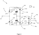
- a chain-link module according to a first embodiment of the invention is designated generally by reference numeral 10.
- the chain-link module 10 includes a first pair 12 of series-conducted switching elements, i.e. series-connected first and second switching elements 14A, 14B, that are separated by a first connection terminal 16, and which are also connected in parallel with first and second series-connected energy storage devices 18, 20.
- the chain-link module 10 also includes a second pair 22 of series-connected switching elements, i.e. series-connected third and fourth switching elements 14C, 14D, which are separated by a second connection terminal 24.
- the second pair 22 of switching elements 14C, 14D is connected in parallel with only one of the first and second energy storage devices 18, 20.
- this is the second energy storage device 20, although in other embodiments of the invention (not shown) the second pair of switching elements may instead be connected in parallel with only the first energy storage device.
- the first switching element 14A includes a first semiconductor device, in the form of a first IGBT 26A, which is connected in parallel with a first anti-parallel diode 28A.
- the second, third and fourth switching elements 14B, 14C, 14D similarly include corresponding second, third and fourth IGBTs 26B, 26C, 26D that are connected in parallel with a corresponding second, third or fourth anti-parallel diode 28B, 28C, 28D.
- each switching element 14A, 14B, 14C, 14D can be considered an active switching element because it can be turned on and off, at will, by a control signal.
- a passive current check element alone, which instead requires a biasing voltage to be applied across its conduction terminals in order to cause it to allow or block the flow of current therethrough. It is not always possible to provide such a biasing voltage, and so such passive elements cannot be turned on and off at will.
- each of the switching elements 14A, 14B, 14C, 14D shares the same configuration in that each includes an IGBT 26A, 26B, 26C, 26D arranged in parallel with a corresponding anti-parallel diode 28A, 28B, 28C, 28D, although this need not necessarily be the case in other embodiments of the invention.
- one or more other types of self-commutated semiconductor devices such as a gate turn-off thyristor (GTO), a field effect transistor (FET), a metal-oxide-semiconductor field-effect transistor (MOSFET), an injection-enhanced gate transistor (IEGT), an integrated gate commutated thyristor (IGCT), a bimode insulated gate transistor (BIGT) or any other self-commutated switching device instead of an IGBT.
- one or more of the semiconductor devices may instead include a wide-bandgap material such as, but not limited to, silicon carbide, boron nitride, gallium nitride and aluminium nitride.
- the number of semiconductor devices in each switching element 14A, 14B, 14C, 14D may vary depending on the required voltage and current ratings of that switching element 14A, 14B, 14C, 14D.
- Alternative passive current check elements i.e. alternatives to the anti-parallel diodes 28A, 28B, 28C, 28D may also be included in other embodiments of the invention, e.g. any alternative element that is capable of limiting current flow in only one direction.
- the number of passive current check elements in each switching element 14A, 14B, 14C, 14D may vary too depending on the required voltage and current ratings of that switching element 14A, 14B, 14C, 14D.
- each of the switching elements in the second pair 20 of switching elements i.e. each of the third and fourth switching elements 14C, 14D
- each of the first and second switching elements 14A, 14B may be rated at 6.5 kV, while the third and fourth switching elements 14C, 14D may be less expensive and less lossy 3.3 kV rated switching elements.
- first and second energy storage devices 18, 20 take the form of corresponding first and second capacitors 30, 32, although other types of energy storage device, i.e. other types of device capable of storing and releasing energy to selectively provide a voltage, e.g. a fuel cell or battery, may be used.
- each energy storage device 18, 20, i.e. each of the first and second capacitors 30, 32 has a corresponding first or second selectively operable rapid discharge circuit 34, 36 connected therewith, and more particularly connected in parallel therewith.
- the first rapid discharge circuit 34 is formed from a further, fifth switching element 14E comprising a fifth IGBT 26E connected in parallel with a fifth anti-parallel diode 28E, which in turn is connected in series with an energy dissipating element in the form of a first resistor 38.
- the second rapid discharge circuit 36 similarly is formed from a sixth switching element 14F, comprising a sixth IGBT 26F connected in parallel with a sixth anti-parallel diode 28F, arranged in series with a second resistor 40.
- the fifth and sixth switching elements 14E, 14F may have the same rating as the third and fourth switching elements 14C, 14D, e.g. 3.3 kV, although this need not necessarily be the case.
- the fifth and sixth switching elements and anti-parallel diodes 14E, 14F, 28E, 28F may also differ in the same manner as described hereinabove, and other forms of energy dissipating element may also be used in other embodiments of the invention (not shown).
- the first to fourth switching elements 14A, 14B, 14C, 14D are selectively switched, e.g. by a module controller 42 programmed to control such switching, in order to direct current I through the chain-link module 10 along different current flow paths in order to cause the chain-link module 10 to provide a positive, zero and negative voltage.
- switching on of the first and fourth switching elements 14A, 14D i.e. switching on of the corresponding first and fourth IGBTs 26A, 26D therein, directs current I in a first direction 44 through the chain-link module 10 from the second connection terminal 24 to the first connection terminal 16 and through both of the first and second energy storage devices 18, 20, i.e. through both of the first and second capacitors 30, 32, as shown schematically in Figure 2(a) .
- This causes the chain-link module 10 to provide a positive voltage with a first magnitude which is commensurate with the combined energy, i.e. equal to the sum of the voltages, stored by the first and second capacitors 30, 32.
- Such a positive voltage contributes towards the provision of a regular voltage by a chain-link converter within which the chain-link module 10 is, in use, included, and thereby facilitates normal power transfer by an associated voltage source converter within which the said chain-link converter is, in turn, incorporated.
- such a positive voltage can be used to oppose, and subsequently extinguish, a DC fault current I F flowing in a second direction 46, opposite the first direction 44, through the chain-link module 10 from the first connection terminal 16 to the second connection terminal 24.
- switching on of the second and third switching elements 14B, 14C directs current I in the second direction 46 through the chain-link module 10, i.e. from the first terminal 16 to the second terminal 24, and through only the second capacitor 32, as shown schematically in Figure 2(d) .
- This causes the chain-link module to provide a negative voltage with a second magnitude that is commensurate with the energy stored by only the second capacitor 32, i.e. equal to the voltage stored by only the second capacitor 32.
- Such a negative voltage can, nevertheless, still be used to oppose, and subsequently extinguish, a DC fault current I F flowing in the first direction 44 through the chain-link module 10 from the second terminal 24 to the first terminal 16.
- the first and second capacitors 30, 32 i.e. the first and second energy storage devices 18, 20 store the same amount of energy, i.e. are charged to the same voltage
- the first magnitude of the positive voltage is double the second magnitude of the negative voltage.
- the first magnitude of the positive voltage is not exactly double the second magnitude of the negative voltage.
- the first capacitor 30 may be controlled to store a voltage of 1.8 kV, while the second capacitor 32 is controlled to store a larger voltage of 2.2 kV.
- the first magnitude of the positive voltage will remain as the sum of the voltages stored by the first and second capacitors 30, 32, e.g. 4.0 kV, while the second magnitude of the negative voltage will be more than half of the positive voltage, i.e. will be equal to the voltage stored by the second capacitor 32, e.g. will be 2.2 kV.
- the third switching element 14C i.e. the third IGBT 26C therein, may be switched on to direct current I to flow in the second direction 46 from the first connection terminal 16, through the first anti-parallel diode 28, through only the first capacitor 30 and, through the said third IGBT 26C to the second connection terminal 24.
- the first switching element 14A i.e. the first IGBT 26A therein, may be switched on to directing current I to flow in the first direction 44 from the second connection terminal 24, through the third anti-parallel diode 28C, through only the first capacitor 30 and, through the said first IGBT 26A to the first connection terminal.
- Directing current I to flow through only the first capacitor 30 in either of the foregoing manners, may be used for a short duration to adjust the ratio of energies stored by the first and second capacitors 30, 32.
- one or other, or both, of the rapid discharge circuits 34, 36 may be triggered, i.e. by turning on the IGBT 26E, 26F in the corresponding fifth or sixth switching element 14E, 14F to remove energy, i.e. voltage, from the energy storage device 18, 20, i.e. capacitor 30, 32 with which it is connected.
- a voltage source converter (not shown) comprises at least one chain-link converter having a plurality of series-connected chain-link modules, at least one of the said chain-link modules being a chain-link module 10, as described hereinabove.
Abstract
(i) directs current (I) through the first and second energy storage devices (18, 20), whereby the chain-link module (10) provides a positive voltage across the first and second connection terminals (16, 24);
(ii) causes current (I) to bypass the first and second energy storage devices (18, 20) whereby the chain-link module (10) provides zero voltage; and
(iii) directs current (I) through the one of the first and second energy storage devices (18, 20) with which the second pair (22) of switching elements (14C, 14D) is connected in parallel, whereby the chain-link module (10) provides a negative voltage across the first and second connection terminals (14, 24).
Description
- This invention relates to a chain-link module, for connection in series with other chain-link modules to form a chain-link converter selectively operable to provide a stepped variable voltage source within a voltage source converter, and to such a voltage source converter.
- In HVDC power transmission networks AC power is typically converted to DC power for transmission via overhead lines, under-sea cables and/or underground cables. This conversion removes the need to compensate for the AC capacitive load effects imposed by the power transmission medium, i.e. the transmission line or cable, and reduces the cost per kilometre of the lines and/or cables, and thus becomes cost-effective when power needs to be transmitted over a long distance. DC power is also transmitted directly from offshore wind parks to onshore AC power transmission networks.
- The conversion between DC power and AC power is utilized where it is necessary to interconnect DC and AC networks. In any such power transmission network, converters (i.e. power converters) are required at each interface between AC and DC power to effect the required conversion from AC to DC or from DC to AC.
- One type of power converter is a voltage source converter, although other types of power converter are also possible.
- Such a voltage source converter includes first and second DC terminals between which extends at least one converter limb, and typically three converter limbs each of which corresponds to a given phase of a three-phase electrical power system.
- The or each converter limb includes first and second limb portions which are separated by an AC terminal.
- In use the first and second DC terminals are connected to a DC network, and the or each AC terminal is connected to a corresponding phase of an AC network.
- Each limb portion includes a chain-link converter which extends between the associated AC terminal and a corresponding one of the first or the second DC terminal. Each chain-link converter includes a plurality of series connected chain-link modules, while each chain-link module includes a number of switching elements which are connected in parallel with an energy storage device, usually in the form of a capacitor. Other types of energy storage device, i.e. any device that is capable of storing and releasing energy to selectively provide a voltage, e.g. a fuel cell or battery, may also be used however.
- The provision of a plurality of chain-link modules means that it is possible to build up a combined voltage across each chain-link converter, via the insertion of the energy storage devices, i.e. the capacitors, of multiple chain-link modules (with each chain-link module providing its own voltage), which is higher than the voltage available from each individual chain-link module.
- Accordingly, each of the chain-link modules work together to permit the chain-link converter to provide a stepped variable voltage source. This permits the generation of a voltage waveform across each chain-link converter using a step-wise approximation. As such each chain-link converter is capable of providing a wide range of complex waveforms.
- For example, operation of each chain-link converter in the foregoing manner can be used to generate an AC voltage waveform at the or each AC terminal, and thereby enable the voltage source converter to provide the aforementioned power transfer functionality between the AC and DC networks.
- According to a first aspect of the invention there is provided a chain-link module, for connection in series with other chain-link modules to form a chain-link converter selectively operable to provide a stepped variable voltage source within a voltage source converter, the chain-link module comprising:
- a first pair of series-connected switching elements separated by a first connection terminal and connected in parallel with first and second series-connected energy storage devices; and
- a second pair of series-connected switching elements separated by a second connection terminal and connected in parallel with one or other of the first and second energy storage devices;
- switching of the switching elements, in use, selectively
- (i) directing current through the first and second energy storage devices, whereby the chain-link module provides a positive voltage across the first and second connection terminals;
- (ii) causing current to bypass the first and second energy storage devices whereby the chain-link module provides zero voltage; and
- (iii) directing current through the one of the first and second energy storage devices with which the second pair of switching elements is connected in parallel, whereby the chain-link module provides a negative voltage across the first and second connection terminals.
- Having a chain-link module that is able to provide a positive voltage is desirable because it allows a chain-link converter within which the module is located to generate a regular voltage of the type that is needed for normal power transmission by an associated voltage source converter. Such a positive voltage can also be used to oppose a fault current flowing from the first connection terminal to the second connection terminal.
- In addition, arranging the second pair of series-connected switching elements in parallel with only one of the energy storage devices, and separating them with the second connection terminal, means that when such a positive voltage is being provided (i.e. during normal power transmission by an associated voltage source converter) current can be directed through both energy storage devices, as required, via only two switching elements.
- Hence, a conduction ratio of one switching element in series per energy storage device is achieved. This results in the chain-link module of the invention having lower conduction losses than, e.g. other chain-link modules with a greater equivalent number of switching elements conducting in series per energy storage device, when providing a positive voltage for normal power transmission by a corresponding associated voltage source converter.
- Moreover, arranging the second pair of switching elements in the aforementioned manner permits the use of selective switching of those switching elements, while the chain-link module is otherwise providing a positive voltage during normal power transmission, to alter the ratio of energy stored by each of the first and second energy storage devices. For example, such selective switching of the switching elements may be used to re-balance the energy stored by each energy storage device, which is desirable in some operating circumstances.
- Meanwhile, the ability of the chain-link module to selectively provide a negative voltage is advantageous because it can be used to oppose a DC fault current flowing through the chain-link module from the second connection terminal to the first connection terminal and so, in conjunction with the aforementioned positive voltage capability, enables a chain-link converter within which the module is, in use, located (and hence also an associated voltage source converter including such a chain-link converter) to provide full DC fault clearing functionality, i.e. the ability to clear DC fault currents flowing in either direction between the first and second connection terminals. Thus, the need otherwise for expensive and space-consuming DC circuit breakers is avoided.
- A further benefit is that such DC fault clearing functionality can be provided using a plurality of identical chain-link modules of the invention within an associated chain-link converter. This simplifies the manufacture and subsequent control of such a chain-link converter compared to, e.g. a chain-link converter incorporating chain-link modules that differ from one another.
- Moreover, being able to selectively provide a negative voltage also allows first and second chain-link converters (having one or more chain-link modules of the invention therein) to work together in a converter limb of an associated voltage source converter to over-modulate, i.e. generate a positive converter limb voltage which is greater than the DC operating voltage of a corresponding DC network with which the voltage source converter is connected, or generate a negative converter limb voltage.
- Preferably at least one of the energy storage devices has a selectively operable rapid discharge circuit connected therewith.
- The inclusion of one or more such rapid discharge circuits advantageously permits, e.g. in emergency conditions, the removal of excess stored energy from the corresponding energy storage device.
- For example, when providing a negative voltage to oppose a DC fault current flowing from the second connection terminal to the first connection terminal, the energy stored by the said one of the first and second energy storage devices (with which the second pair of switching elements are connected in parallel) will rise transiently as a result of inductive energy being stored as the fault current is suppressed, and the triggering, i.e. selective operation, of a rapid discharge circuit connected with the said storage device affected by the additional inductive energy, can be used to reduce the amount of energy stored.
- In a preferred embodiment of the invention each energy storage device has a selectively operable rapid discharge circuit connected therewith.
- Providing each energy storage device with a rapid discharge circuit allows the energy stored by each energy storage device to be reduced, as mentioned hereinabove. In addition, however, each energy storage device having a rapid discharge circuit also permits the relative ratio of energy stored by the first and second energy storage devices to be altered, e.g. to re-balance the energy so stored.
- Optionally at least one of the switching elements in the second pair of switching elements has a lower voltage rating than one or both of the switching elements in the first pair of switching elements.
- The positive voltage provided by the chain-link module has a first magnitude that is commensurate with the combined energy stored by the first and second energy storage devices, whereas the negative voltage provided has a second magnitude which is commensurate with only the energy stored by the said one of the first and second energy storage devices with which the second pair of switching elements is connected in parallel. The second magnitude is therefore lower than the first magnitude, and so the voltage that must be supported by the second pair of switching elements is also lower than that which has to be supported by the first pair of switching elements.
- In turn, this can be exploited by including one or more switching elements in the second pair with a lower voltage rating, which advantageously reduces both the cost and power losses associated with the or each said lower voltage rated switching element.
- The chain-link module may further include a module controller programmed to cause the first and second energy storage devices to store different amounts of energy.
- Having the first and second energy storage devices store different amounts of energy advantageously allows for a tuning of an associated DC fault clearing functionality.
- For example, having the energy storage device connected in parallel with the second pair of switching elements store more energy than the other energy storage device means that the negative voltage provided by the chain-link module is larger than would be the case if both energy storage devices stored the same amount of energy. A consequence of being able to provide such a larger negative voltage is that it achieves more rapid DC fault clearing.
- According to a second aspect of the invention there is provided a voltage source converter comprising at least one chain-link converter having a plurality of series-connected chain link modules, at least one of the said chain-link modules being a chain-link module as described hereinabove.
- The voltage source converter of the invention shares the benefits of the corresponding features of the chain-link module of the invention.
- It will be appreciated that the use of the terms "first" and "second", and the like, in this patent specification is merely intended to help distinguish between similar features (e.g. the first and second series-connected energy storage devices), and is not intended to indicate the relative importance of one feature over another feature, unless otherwise specified.
- Within the scope of this application it is expressly intended that the various aspects, embodiments, examples and alternatives set out in the preceding paragraphs, and the claims and/or the following description and drawings, and in particular the individual features thereof, may be taken independently or in any combination. That is, all embodiments and all features of any embodiment can be combined in any way and/or combination, unless such features are incompatible. The applicant reserves the right to change any originally filed claim or file any new claim accordingly, including the right to amend any originally filed claim to depend from and/or incorporate any feature of any other claim although not originally claimed in that manner.
- There now follows a brief description of preferred embodiments of the invention, by way of non-limiting example, with reference being made to the following figures in which:
-
Figure 1 shows a chain-link module according to an embodiment of the invention; and -
Figures 2(a) to 2(d) illustrate different current flow paths through the chain-link module shown inFigure 1 , whereby the chain-link module is able to provide a positive, zero and negative voltage. - A chain-link module according to a first embodiment of the invention is designated generally by
reference numeral 10. - The chain-
link module 10 includes afirst pair 12 of series-conducted switching elements, i.e. series-connected first andsecond switching elements first connection terminal 16, and which are also connected in parallel with first and second series-connected energy storage devices 18, 20. - The chain-
link module 10 also includes asecond pair 22 of series-connected switching elements, i.e. series-connected third andfourth switching elements second connection terminal 24. - In contrast to the
first pair 12 ofswitching elements second pair 22 ofswitching elements - The
first switching element 14A includes a first semiconductor device, in the form of afirst IGBT 26A, which is connected in parallel with a first anti-parallel diode 28A. The second, third andfourth switching elements - The inclusion of such a self-commutated semiconductor device, i.e. IGBT, in each switching
element element - Returning to the embodiment shown, each of the
switching elements IGBT 26A, 26B, 26C, 26D arranged in parallel with a corresponding anti-parallel diode 28A, 28B, 28C, 28D, although this need not necessarily be the case in other embodiments of the invention. - For example, it is possible to use one or more other types of self-commutated semiconductor devices, such as a gate turn-off thyristor (GTO), a field effect transistor (FET), a metal-oxide-semiconductor field-effect transistor (MOSFET), an injection-enhanced gate transistor (IEGT), an integrated gate commutated thyristor (IGCT), a bimode insulated gate transistor (BIGT) or any other self-commutated switching device instead of an IGBT. In addition, one or more of the semiconductor devices may instead include a wide-bandgap material such as, but not limited to, silicon carbide, boron nitride, gallium nitride and aluminium nitride.
- The number of semiconductor devices in each switching
element element - Alternative passive current check elements, i.e. alternatives to the anti-parallel diodes 28A, 28B, 28C, 28D may also be included in other embodiments of the invention, e.g. any alternative element that is capable of limiting current flow in only one direction. The number of passive current check elements in each switching
element element - In the particular embodiment shown, each of the switching elements in the second pair 20 of switching elements, i.e. each of the third and
fourth switching elements second switching elements second switching elements fourth switching elements - Meanwhile, the first and second energy storage devices 18, 20 take the form of corresponding first and second capacitors 30, 32, although other types of energy storage device, i.e. other types of device capable of storing and releasing energy to selectively provide a voltage, e.g. a fuel cell or battery, may be used.
- In addition to the foregoing, each energy storage device 18, 20, i.e. each of the first and second capacitors 30, 32 has a corresponding first or second selectively operable
rapid discharge circuit - The first
rapid discharge circuit 34 is formed from a further,fifth switching element 14E comprising afifth IGBT 26E connected in parallel with a fifthanti-parallel diode 28E, which in turn is connected in series with an energy dissipating element in the form of afirst resistor 38. - The second
rapid discharge circuit 36 similarly is formed from a sixth switching element 14F, comprising asixth IGBT 26F connected in parallel with a sixth anti-parallel diode 28F, arranged in series with a second resistor 40. - The fifth and
sixth switching elements 14E, 14F may have the same rating as the third andfourth switching elements - The fifth and sixth switching elements and
anti-parallel diodes - In use, the first to
fourth switching elements module controller 42 programmed to control such switching, in order to direct current I through the chain-link module 10 along different current flow paths in order to cause the chain-link module 10 to provide a positive, zero and negative voltage. - More particularly, switching on of the first and
fourth switching elements fourth IGBTs 26A, 26D therein, directs current I in afirst direction 44 through the chain-link module 10 from thesecond connection terminal 24 to thefirst connection terminal 16 and through both of the first and second energy storage devices 18, 20, i.e. through both of the first and second capacitors 30, 32, as shown schematically inFigure 2(a) . This causes the chain-link module 10 to provide a positive voltage with a first magnitude which is commensurate with the combined energy, i.e. equal to the sum of the voltages, stored by the first and second capacitors 30, 32. - Such a positive voltage contributes towards the provision of a regular voltage by a chain-link converter within which the chain-
link module 10 is, in use, included, and thereby facilitates normal power transfer by an associated voltage source converter within which the said chain-link converter is, in turn, incorporated. - In addition, such a positive voltage can be used to oppose, and subsequently extinguish, a DC fault current IF flowing in a
second direction 46, opposite thefirst direction 44, through the chain-link module 10 from thefirst connection terminal 16 to thesecond connection terminal 24. - In the meantime, switching on of only the
second switching element 14B, i.e. the second IGBT 26B therein, causes current I flowing in thesecond direction 46 through the chain-link module 10 to bypass both capacitors 30, 32, as shown schematically inFigure 2(b) , and thereby causes the chain-link module 10 to provide zero voltage. - Similarly, switching on of only the
fourth switching element 14D, i.e. the fourth IGBT 26D therein, causes current I flowing in thefirst direction 44 through the chain-link module 10 to bypass both capacitors, 30, 32, as shown schematically inFigure 2(c) , and thereby again causes the chain-link module to provide zero voltage. - Meanwhile, switching on of the second and
third switching elements second direction 46 through the chain-link module 10, i.e. from thefirst terminal 16 to thesecond terminal 24, and through only the second capacitor 32, as shown schematically inFigure 2(d) . This causes the chain-link module to provide a negative voltage with a second magnitude that is commensurate with the energy stored by only the second capacitor 32, i.e. equal to the voltage stored by only the second capacitor 32. - Such a negative voltage can, nevertheless, still be used to oppose, and subsequently extinguish, a DC fault current IF flowing in the
first direction 44 through the chain-link module 10 from thesecond terminal 24 to thefirst terminal 16. - In circumstances where the first and second capacitors 30, 32, i.e. the first and second energy storage devices 18, 20, store the same amount of energy, i.e. are charged to the same voltage, the first magnitude of the positive voltage is double the second magnitude of the negative voltage.
- In other embodiments, e.g. in which the
module controller 42 is programmed to cause the first and second energy storage devices 18, 20, i.e. the first and second capacitors 30, 32, to store different amounts of energy, the first magnitude of the positive voltage is not exactly double the second magnitude of the negative voltage. - For example, the first capacitor 30 may be controlled to store a voltage of 1.8 kV, while the second capacitor 32 is controlled to store a larger voltage of 2.2 kV. In such circumstances, the first magnitude of the positive voltage will remain as the sum of the voltages stored by the first and second capacitors 30, 32, e.g. 4.0 kV, while the second magnitude of the negative voltage will be more than half of the positive voltage, i.e. will be equal to the voltage stored by the second capacitor 32, e.g. will be 2.2 kV.
- In addition to the foregoing, the
third switching element 14C, i.e. the third IGBT 26C therein, may be switched on to direct current I to flow in thesecond direction 46 from thefirst connection terminal 16, through the first anti-parallel diode 28, through only the first capacitor 30 and, through the said third IGBT 26C to thesecond connection terminal 24. - Alternatively, the
first switching element 14A, i.e. thefirst IGBT 26A therein, may be switched on to directing current I to flow in thefirst direction 44 from thesecond connection terminal 24, through the third anti-parallel diode 28C, through only the first capacitor 30 and, through the saidfirst IGBT 26A to the first connection terminal. - Directing current I to flow through only the first capacitor 30 in either of the foregoing manners, may be used for a short duration to adjust the ratio of energies stored by the first and second capacitors 30, 32.
- It may also be used, perhaps only for a few microseconds at a time, to provide a transition between a fully bypassed chain-
link module 10 providing zero voltage, and one providing a full positive voltage of the first magnitude, e.g. in order to reduce the size of voltage step imposed on an associated external system. - Additionally, in use, one or other, or both, of the
rapid discharge circuits IGBT sixth switching element 14E, 14F to remove energy, i.e. voltage, from the energy storage device 18, 20, i.e. capacitor 30, 32 with which it is connected. - A voltage source converter according to a second embodiment of the invention (not shown) comprises at least one chain-link converter having a plurality of series-connected chain-link modules, at least one of the said chain-link modules being a chain-
link module 10, as described hereinabove.
Claims (6)
- A chain-link module (10), for connection in series with other chain-link modules to form a chain-link converter selectively operable to provide a stepped variable voltage source within a voltage source converter, the chain-link module comprising:a first pair (12) of series-connected switching elements (14A, 14B) separated by a first connection terminal (16) and connected in parallel with first and second series-connected energy storage devices (18, 20); anda second pair (22) of series-connected switching elements (14C, 14D) separated by a second connection terminal (24) and connected in parallel with one or other of the first and second energy storage devices (18, 20);switching of the switching elements (14A, 14B, 14C, 14D), in use, selectively:(i) directing current (I) through the first and second energy storage devices (18, 20), whereby the chain-link module (10) provides a positive voltage across the first and second connection terminals (16, 24);(ii) causing current (I) to bypass the first and second energy storage devices (18, 20) whereby the chain-link module (10) provides zero voltage; and(iii) directing current (I) through the one of the first and second energy storage devices (18, 20) with which the second pair (22) of switching elements (14C, 14D) is connected in parallel, whereby the chain-link module (10) provides a negative voltage across the first and second connection terminals (14, 24).
- A chain-link module (10) according to Claim 1 wherein at least one of the energy storage devices (18, 20) has a selectively operable rapid discharge circuit (34, 36) connected therewith.
- A chain-link module (10) according to Claim 2 wherein each energy storage device (18, 20) has a selectively operable rapid discharge circuit (34, 36) connected therewith.
- A chain-link module (10) according to any preceding claim wherein at least one of the switching elements (14C, 14D) in the second pair (22) of switching elements has a lower voltage rating than one or both of the switching elements (14A, 14B) in the first pair (12) of switching elements.
- A chain-link module (10) according to any preceding claim further including a module controller (42) programmed to cause the first and second energy storage devices (18, 20) to store different amounts of energy.
- A voltage source converter comprising at least one chain-link converter having a plurality of series-connected chain link modules, at least one of the said chain-link modules being a chain-link module (10) according to any preceding claim.
Priority Applications (4)
| Application Number | Priority Date | Filing Date | Title |
|---|---|---|---|
| EP20275020.4A EP3859965B1 (en) | 2020-01-30 | 2020-01-30 | Improvements in or relating to chain-link modules for voltage source converters |
| US17/795,683 US20230119315A1 (en) | 2020-01-30 | 2021-01-25 | Improvements in or relating to chain-link modules for voltage source converters |
| PCT/EP2021/051575 WO2021151819A1 (en) | 2020-01-30 | 2021-01-25 | Improvements in or relating to chain-link modules for voltage source converters |
| CN202180011752.6A CN114982120A (en) | 2020-01-30 | 2021-01-25 | Improvements in or relating to chain-link modules for voltage source converters |
Applications Claiming Priority (1)
| Application Number | Priority Date | Filing Date | Title |
|---|---|---|---|
| EP20275020.4A EP3859965B1 (en) | 2020-01-30 | 2020-01-30 | Improvements in or relating to chain-link modules for voltage source converters |
Publications (2)
| Publication Number | Publication Date |
|---|---|
| EP3859965A1 true EP3859965A1 (en) | 2021-08-04 |
| EP3859965B1 EP3859965B1 (en) | 2023-09-06 |
Family
ID=69423242
Family Applications (1)
| Application Number | Title | Priority Date | Filing Date |
|---|---|---|---|
| EP20275020.4A Active EP3859965B1 (en) | 2020-01-30 | 2020-01-30 | Improvements in or relating to chain-link modules for voltage source converters |
Country Status (4)
| Country | Link |
|---|---|
| US (1) | US20230119315A1 (en) |
| EP (1) | EP3859965B1 (en) |
| CN (1) | CN114982120A (en) |
| WO (1) | WO2021151819A1 (en) |
Citations (5)
| Publication number | Priority date | Publication date | Assignee | Title |
|---|---|---|---|---|
| CN101051751A (en) * | 2007-05-14 | 2007-10-10 | 上海艾帕电力电子有限公司 | Active power filter including power unit and its control method |
| CN106998151A (en) * | 2017-04-21 | 2017-08-01 | 上海交通大学 | Multilevel converter based on asymmetric Shuangzi module and half-bridge submodule |
| EP3373438A1 (en) * | 2015-11-03 | 2018-09-12 | Hyosung Corporation | Capacitor discharge device inside sub module of mmc converter |
| CN109120174A (en) * | 2018-09-03 | 2019-01-01 | 国网山东省电力公司潍坊供电公司 | Capacitance voltage equalization methods based on Shuangzi MMC module |
| CN106877718B (en) * | 2017-04-21 | 2019-04-05 | 上海交通大学 | Modularization multi-level converter asymmetry Shuangzi module midpoint potential balance control method |
Family Cites Families (5)
| Publication number | Priority date | Publication date | Assignee | Title |
|---|---|---|---|---|
| EP2852040A1 (en) * | 2013-09-20 | 2015-03-25 | Alstom Technology Ltd | Module |
| US10069430B2 (en) * | 2013-11-07 | 2018-09-04 | Regents Of The University Of Minnesota | Modular converter with multilevel submodules |
| EP3662572A1 (en) * | 2017-09-28 | 2020-06-10 | Siemens Aktiengesellschaft | Submodule for a modular multilevel converter |
| EP3544163B1 (en) * | 2018-03-21 | 2020-09-16 | General Electric Technology GmbH | Converter |
| EP3547525A1 (en) * | 2018-03-27 | 2019-10-02 | General Electric Technology GmbH | Voltage source converter apparatus |
-
2020
- 2020-01-30 EP EP20275020.4A patent/EP3859965B1/en active Active
-
2021
- 2021-01-25 US US17/795,683 patent/US20230119315A1/en active Pending
- 2021-01-25 CN CN202180011752.6A patent/CN114982120A/en active Pending
- 2021-01-25 WO PCT/EP2021/051575 patent/WO2021151819A1/en active Application Filing
Patent Citations (5)
| Publication number | Priority date | Publication date | Assignee | Title |
|---|---|---|---|---|
| CN101051751A (en) * | 2007-05-14 | 2007-10-10 | 上海艾帕电力电子有限公司 | Active power filter including power unit and its control method |
| EP3373438A1 (en) * | 2015-11-03 | 2018-09-12 | Hyosung Corporation | Capacitor discharge device inside sub module of mmc converter |
| CN106998151A (en) * | 2017-04-21 | 2017-08-01 | 上海交通大学 | Multilevel converter based on asymmetric Shuangzi module and half-bridge submodule |
| CN106877718B (en) * | 2017-04-21 | 2019-04-05 | 上海交通大学 | Modularization multi-level converter asymmetry Shuangzi module midpoint potential balance control method |
| CN109120174A (en) * | 2018-09-03 | 2019-01-01 | 国网山东省电力公司潍坊供电公司 | Capacitance voltage equalization methods based on Shuangzi MMC module |
Non-Patent Citations (3)
| Title |
|---|
| ADAM GRAIN PHILIP ET AL: "New Efficient Submodule for a Modular Multilevel Converter in Multiterminal HVDC Networks", IEEE TRANSACTIONS ON POWER ELECTRONICS, INSTITUTE OF ELECTRICAL AND ELECTRONICS ENGINEERS, USA, vol. 32, no. 6, 1 June 2017 (2017-06-01), pages 4258 - 4278, XP011640902, ISSN: 0885-8993, [retrieved on 20170210], DOI: 10.1109/TPEL.2016.2603180 * |
| LU MAOZENG ET AL: "Imbalance Mechanism and Balanced Control of Capacitor Voltage for a Hybrid Modular Multilevel Converter", IEEE TRANSACTIONS ON POWER ELECTRONICS, INSTITUTE OF ELECTRICAL AND ELECTRONICS ENGINEERS, USA, vol. 33, no. 7, 1 July 2018 (2018-07-01), pages 5686 - 5696, XP011679873, ISSN: 0885-8993, [retrieved on 20180319], DOI: 10.1109/TPEL.2017.2743780 * |
| NAMI ALIREZA ET AL: "Modular Multilevel Converters for HVDC Applications: Review on Converter Cells and Functionalities", IEEE TRANSACTIONS ON POWER ELECTRONICS, INSTITUTE OF ELECTRICAL AND ELECTRONICS ENGINEERS, USA, vol. 30, no. 1, 1 January 2015 (2015-01-01), pages 18 - 36, XP011557523, ISSN: 0885-8993, [retrieved on 20140826], DOI: 10.1109/TPEL.2014.2327641 * |
Also Published As
| Publication number | Publication date |
|---|---|
| CN114982120A (en) | 2022-08-30 |
| EP3859965B1 (en) | 2023-09-06 |
| WO2021151819A1 (en) | 2021-08-05 |
| US20230119315A1 (en) | 2023-04-20 |
Similar Documents
| Publication | Publication Date | Title |
|---|---|---|
| US11777401B2 (en) | Fault tolerant AC-DC chain-link converter | |
| US20170264187A1 (en) | A voltage source converter | |
| EP2782239A1 (en) | Power electronic converter | |
| US20160164296A1 (en) | Module | |
| US20190068081A1 (en) | Converter | |
| EP2849330A1 (en) | Modular Power Converter and module thereof | |
| WO2015039942A1 (en) | Module | |
| EP2849306A1 (en) | Voltage source converter | |
| WO2018100051A1 (en) | Improvements in or relating to hvdc power converters | |
| EP3859965A1 (en) | Improvements in or relating to chain-link modules for voltage source converters | |
| US20230253796A1 (en) | Improvements in or relating to converter stations | |
| US11721978B2 (en) | Switching valve | |
| EP3890178A1 (en) | Improvements in or relating to chain-link converters | |
| US20210359617A1 (en) | Electrical assembly | |
| US20230188027A1 (en) | Improvements in or relating to chain-link modules for voltage source converters | |
| EP4322390A1 (en) | Controller for power electronic device | |
| US20230054979A1 (en) | Electrical assembly | |
| EP3930171A1 (en) | Module | |
| EP3989429A1 (en) | Electrical assembly | |
| EP3972102A1 (en) | Improvements in or relating to power transmission schemes |
Legal Events
| Date | Code | Title | Description |
|---|---|---|---|
| PUAI | Public reference made under article 153(3) epc to a published international application that has entered the european phase |
Free format text: ORIGINAL CODE: 0009012 |
|
| STAA | Information on the status of an ep patent application or granted ep patent |
Free format text: STATUS: THE APPLICATION HAS BEEN PUBLISHED |
|
| AK | Designated contracting states |
Kind code of ref document: A1 Designated state(s): AL AT BE BG CH CY CZ DE DK EE ES FI FR GB GR HR HU IE IS IT LI LT LU LV MC MK MT NL NO PL PT RO RS SE SI SK SM TR |
|
| RAP3 | Party data changed (applicant data changed or rights of an application transferred) |
Owner name: GENERAL ELECTRIC TECHNOLOGY GMBH |
|
| STAA | Information on the status of an ep patent application or granted ep patent |
Free format text: STATUS: REQUEST FOR EXAMINATION WAS MADE |
|
| 17P | Request for examination filed |
Effective date: 20220201 |
|
| RBV | Designated contracting states (corrected) |
Designated state(s): AL AT BE BG CH CY CZ DE DK EE ES FI FR GB GR HR HU IE IS IT LI LT LU LV MC MK MT NL NO PL PT RO RS SE SI SK SM TR |
|
| GRAP | Despatch of communication of intention to grant a patent |
Free format text: ORIGINAL CODE: EPIDOSNIGR1 |
|
| STAA | Information on the status of an ep patent application or granted ep patent |
Free format text: STATUS: GRANT OF PATENT IS INTENDED |
|
| INTG | Intention to grant announced |
Effective date: 20220610 |
|
| GRAJ | Information related to disapproval of communication of intention to grant by the applicant or resumption of examination proceedings by the epo deleted |
Free format text: ORIGINAL CODE: EPIDOSDIGR1 |
|
| STAA | Information on the status of an ep patent application or granted ep patent |
Free format text: STATUS: REQUEST FOR EXAMINATION WAS MADE |
|
| INTC | Intention to grant announced (deleted) | ||
| GRAP | Despatch of communication of intention to grant a patent |
Free format text: ORIGINAL CODE: EPIDOSNIGR1 |
|
| STAA | Information on the status of an ep patent application or granted ep patent |
Free format text: STATUS: GRANT OF PATENT IS INTENDED |
|
| INTG | Intention to grant announced |
Effective date: 20230404 |
|
| P01 | Opt-out of the competence of the unified patent court (upc) registered |
Effective date: 20230522 |
|
| GRAS | Grant fee paid |
Free format text: ORIGINAL CODE: EPIDOSNIGR3 |
|
| GRAA | (expected) grant |
Free format text: ORIGINAL CODE: 0009210 |
|
| STAA | Information on the status of an ep patent application or granted ep patent |
Free format text: STATUS: THE PATENT HAS BEEN GRANTED |
|
| AK | Designated contracting states |
Kind code of ref document: B1 Designated state(s): AL AT BE BG CH CY CZ DE DK EE ES FI FR GB GR HR HU IE IS IT LI LT LU LV MC MK MT NL NO PL PT RO RS SE SI SK SM TR |
|
| REG | Reference to a national code |
Ref country code: GB Ref legal event code: FG4D |
|
| REG | Reference to a national code |
Ref country code: CH Ref legal event code: EP |
|
| REG | Reference to a national code |
Ref country code: DE Ref legal event code: R096 Ref document number: 602020017171 Country of ref document: DE |
|
| REG | Reference to a national code |
Ref country code: IE Ref legal event code: FG4D |
|
| REG | Reference to a national code |
Ref country code: SE Ref legal event code: TRGR |
|
| REG | Reference to a national code |
Ref country code: LT Ref legal event code: MG9D |
|
| REG | Reference to a national code |
Ref country code: NL Ref legal event code: MP Effective date: 20230906 |
|
| PG25 | Lapsed in a contracting state [announced via postgrant information from national office to epo] |
Ref country code: GR Free format text: LAPSE BECAUSE OF FAILURE TO SUBMIT A TRANSLATION OF THE DESCRIPTION OR TO PAY THE FEE WITHIN THE PRESCRIBED TIME-LIMIT Effective date: 20231207 |
|
| PGFP | Annual fee paid to national office [announced via postgrant information from national office to epo] |
Ref country code: GB Payment date: 20231219 Year of fee payment: 5 |
|
| PG25 | Lapsed in a contracting state [announced via postgrant information from national office to epo] |
Ref country code: RS Free format text: LAPSE BECAUSE OF FAILURE TO SUBMIT A TRANSLATION OF THE DESCRIPTION OR TO PAY THE FEE WITHIN THE PRESCRIBED TIME-LIMIT Effective date: 20230906 Ref country code: NO Free format text: LAPSE BECAUSE OF FAILURE TO SUBMIT A TRANSLATION OF THE DESCRIPTION OR TO PAY THE FEE WITHIN THE PRESCRIBED TIME-LIMIT Effective date: 20231206 Ref country code: LV Free format text: LAPSE BECAUSE OF FAILURE TO SUBMIT A TRANSLATION OF THE DESCRIPTION OR TO PAY THE FEE WITHIN THE PRESCRIBED TIME-LIMIT Effective date: 20230906 Ref country code: LT Free format text: LAPSE BECAUSE OF FAILURE TO SUBMIT A TRANSLATION OF THE DESCRIPTION OR TO PAY THE FEE WITHIN THE PRESCRIBED TIME-LIMIT Effective date: 20230906 Ref country code: HR Free format text: LAPSE BECAUSE OF FAILURE TO SUBMIT A TRANSLATION OF THE DESCRIPTION OR TO PAY THE FEE WITHIN THE PRESCRIBED TIME-LIMIT Effective date: 20230906 Ref country code: GR Free format text: LAPSE BECAUSE OF FAILURE TO SUBMIT A TRANSLATION OF THE DESCRIPTION OR TO PAY THE FEE WITHIN THE PRESCRIBED TIME-LIMIT Effective date: 20231207 Ref country code: FI Free format text: LAPSE BECAUSE OF FAILURE TO SUBMIT A TRANSLATION OF THE DESCRIPTION OR TO PAY THE FEE WITHIN THE PRESCRIBED TIME-LIMIT Effective date: 20230906 |
|
| PGFP | Annual fee paid to national office [announced via postgrant information from national office to epo] |
Ref country code: SE Payment date: 20231219 Year of fee payment: 5 Ref country code: FR Payment date: 20231219 Year of fee payment: 5 |
|
| REG | Reference to a national code |
Ref country code: AT Ref legal event code: MK05 Ref document number: 1609835 Country of ref document: AT Kind code of ref document: T Effective date: 20230906 |
|
| PG25 | Lapsed in a contracting state [announced via postgrant information from national office to epo] |
Ref country code: NL Free format text: LAPSE BECAUSE OF FAILURE TO SUBMIT A TRANSLATION OF THE DESCRIPTION OR TO PAY THE FEE WITHIN THE PRESCRIBED TIME-LIMIT Effective date: 20230906 |
|
| PG25 | Lapsed in a contracting state [announced via postgrant information from national office to epo] |
Ref country code: IS Free format text: LAPSE BECAUSE OF FAILURE TO SUBMIT A TRANSLATION OF THE DESCRIPTION OR TO PAY THE FEE WITHIN THE PRESCRIBED TIME-LIMIT Effective date: 20240106 |
|
| PG25 | Lapsed in a contracting state [announced via postgrant information from national office to epo] |
Ref country code: AT Free format text: LAPSE BECAUSE OF FAILURE TO SUBMIT A TRANSLATION OF THE DESCRIPTION OR TO PAY THE FEE WITHIN THE PRESCRIBED TIME-LIMIT Effective date: 20230906 |
|
| PG25 | Lapsed in a contracting state [announced via postgrant information from national office to epo] |
Ref country code: ES Free format text: LAPSE BECAUSE OF FAILURE TO SUBMIT A TRANSLATION OF THE DESCRIPTION OR TO PAY THE FEE WITHIN THE PRESCRIBED TIME-LIMIT Effective date: 20230906 |
|
| PG25 | Lapsed in a contracting state [announced via postgrant information from national office to epo] |
Ref country code: SM Free format text: LAPSE BECAUSE OF FAILURE TO SUBMIT A TRANSLATION OF THE DESCRIPTION OR TO PAY THE FEE WITHIN THE PRESCRIBED TIME-LIMIT Effective date: 20230906 Ref country code: RO Free format text: LAPSE BECAUSE OF FAILURE TO SUBMIT A TRANSLATION OF THE DESCRIPTION OR TO PAY THE FEE WITHIN THE PRESCRIBED TIME-LIMIT Effective date: 20230906 Ref country code: IS Free format text: LAPSE BECAUSE OF FAILURE TO SUBMIT A TRANSLATION OF THE DESCRIPTION OR TO PAY THE FEE WITHIN THE PRESCRIBED TIME-LIMIT Effective date: 20240106 Ref country code: ES Free format text: LAPSE BECAUSE OF FAILURE TO SUBMIT A TRANSLATION OF THE DESCRIPTION OR TO PAY THE FEE WITHIN THE PRESCRIBED TIME-LIMIT Effective date: 20230906 Ref country code: EE Free format text: LAPSE BECAUSE OF FAILURE TO SUBMIT A TRANSLATION OF THE DESCRIPTION OR TO PAY THE FEE WITHIN THE PRESCRIBED TIME-LIMIT Effective date: 20230906 Ref country code: CZ Free format text: LAPSE BECAUSE OF FAILURE TO SUBMIT A TRANSLATION OF THE DESCRIPTION OR TO PAY THE FEE WITHIN THE PRESCRIBED TIME-LIMIT Effective date: 20230906 Ref country code: AT Free format text: LAPSE BECAUSE OF FAILURE TO SUBMIT A TRANSLATION OF THE DESCRIPTION OR TO PAY THE FEE WITHIN THE PRESCRIBED TIME-LIMIT Effective date: 20230906 Ref country code: SK Free format text: LAPSE BECAUSE OF FAILURE TO SUBMIT A TRANSLATION OF THE DESCRIPTION OR TO PAY THE FEE WITHIN THE PRESCRIBED TIME-LIMIT Effective date: 20230906 Ref country code: PT Free format text: LAPSE BECAUSE OF FAILURE TO SUBMIT A TRANSLATION OF THE DESCRIPTION OR TO PAY THE FEE WITHIN THE PRESCRIBED TIME-LIMIT Effective date: 20240108 |
|
| PGFP | Annual fee paid to national office [announced via postgrant information from national office to epo] |
Ref country code: DE Payment date: 20231219 Year of fee payment: 5 |