EP3859789A1 - Vertical conduction electronic power device having a reduced on resistance and manufacturing process thereof - Google Patents
Vertical conduction electronic power device having a reduced on resistance and manufacturing process thereof Download PDFInfo
- Publication number
- EP3859789A1 EP3859789A1 EP21154045.5A EP21154045A EP3859789A1 EP 3859789 A1 EP3859789 A1 EP 3859789A1 EP 21154045 A EP21154045 A EP 21154045A EP 3859789 A1 EP3859789 A1 EP 3859789A1
- Authority
- EP
- European Patent Office
- Prior art keywords
- substrate
- epitaxial layer
- region
- regions
- forming
- Prior art date
- Legal status (The legal status is an assumption and is not a legal conclusion. Google has not performed a legal analysis and makes no representation as to the accuracy of the status listed.)
- Granted
Links
Images



Classifications
-
- H—ELECTRICITY
- H10—SEMICONDUCTOR DEVICES; ELECTRIC SOLID-STATE DEVICES NOT OTHERWISE PROVIDED FOR
- H10D—INORGANIC ELECTRIC SEMICONDUCTOR DEVICES
- H10D30/00—Field-effect transistors [FET]
- H10D30/60—Insulated-gate field-effect transistors [IGFET]
- H10D30/64—Double-diffused metal-oxide semiconductor [DMOS] FETs
- H10D30/66—Vertical DMOS [VDMOS] FETs
-
- H—ELECTRICITY
- H10—SEMICONDUCTOR DEVICES; ELECTRIC SOLID-STATE DEVICES NOT OTHERWISE PROVIDED FOR
- H10D—INORGANIC ELECTRIC SEMICONDUCTOR DEVICES
- H10D30/00—Field-effect transistors [FET]
- H10D30/60—Insulated-gate field-effect transistors [IGFET]
- H10D30/63—Vertical IGFETs
-
- H—ELECTRICITY
- H10—SEMICONDUCTOR DEVICES; ELECTRIC SOLID-STATE DEVICES NOT OTHERWISE PROVIDED FOR
- H10D—INORGANIC ELECTRIC SEMICONDUCTOR DEVICES
- H10D30/00—Field-effect transistors [FET]
- H10D30/01—Manufacture or treatment
- H10D30/021—Manufacture or treatment of FETs having insulated gates [IGFET]
- H10D30/025—Manufacture or treatment of FETs having insulated gates [IGFET] of vertical IGFETs
-
- H—ELECTRICITY
- H10—SEMICONDUCTOR DEVICES; ELECTRIC SOLID-STATE DEVICES NOT OTHERWISE PROVIDED FOR
- H10D—INORGANIC ELECTRIC SEMICONDUCTOR DEVICES
- H10D30/00—Field-effect transistors [FET]
- H10D30/01—Manufacture or treatment
- H10D30/021—Manufacture or treatment of FETs having insulated gates [IGFET]
- H10D30/028—Manufacture or treatment of FETs having insulated gates [IGFET] of double-diffused metal oxide semiconductor [DMOS] FETs
- H10D30/0291—Manufacture or treatment of FETs having insulated gates [IGFET] of double-diffused metal oxide semiconductor [DMOS] FETs of vertical DMOS [VDMOS] FETs
-
- H—ELECTRICITY
- H10—SEMICONDUCTOR DEVICES; ELECTRIC SOLID-STATE DEVICES NOT OTHERWISE PROVIDED FOR
- H10D—INORGANIC ELECTRIC SEMICONDUCTOR DEVICES
- H10D30/00—Field-effect transistors [FET]
- H10D30/01—Manufacture or treatment
- H10D30/021—Manufacture or treatment of FETs having insulated gates [IGFET]
- H10D30/028—Manufacture or treatment of FETs having insulated gates [IGFET] of double-diffused metal oxide semiconductor [DMOS] FETs
- H10D30/0291—Manufacture or treatment of FETs having insulated gates [IGFET] of double-diffused metal oxide semiconductor [DMOS] FETs of vertical DMOS [VDMOS] FETs
- H10D30/0297—Manufacture or treatment of FETs having insulated gates [IGFET] of double-diffused metal oxide semiconductor [DMOS] FETs of vertical DMOS [VDMOS] FETs using recessing of the gate electrodes, e.g. to form trench gate electrodes
-
- H—ELECTRICITY
- H10—SEMICONDUCTOR DEVICES; ELECTRIC SOLID-STATE DEVICES NOT OTHERWISE PROVIDED FOR
- H10D—INORGANIC ELECTRIC SEMICONDUCTOR DEVICES
- H10D30/00—Field-effect transistors [FET]
- H10D30/60—Insulated-gate field-effect transistors [IGFET]
- H10D30/64—Double-diffused metal-oxide semiconductor [DMOS] FETs
- H10D30/66—Vertical DMOS [VDMOS] FETs
- H10D30/668—Vertical DMOS [VDMOS] FETs having trench gate electrodes, e.g. UMOS transistors
-
- H—ELECTRICITY
- H10—SEMICONDUCTOR DEVICES; ELECTRIC SOLID-STATE DEVICES NOT OTHERWISE PROVIDED FOR
- H10D—INORGANIC ELECTRIC SEMICONDUCTOR DEVICES
- H10D62/00—Semiconductor bodies, or regions thereof, of devices having potential barriers
- H10D62/10—Shapes, relative sizes or dispositions of the regions of the semiconductor bodies; Shapes of the semiconductor bodies
- H10D62/124—Shapes, relative sizes or dispositions of the regions of semiconductor bodies or of junctions between the regions
-
- H—ELECTRICITY
- H10—SEMICONDUCTOR DEVICES; ELECTRIC SOLID-STATE DEVICES NOT OTHERWISE PROVIDED FOR
- H10D—INORGANIC ELECTRIC SEMICONDUCTOR DEVICES
- H10D62/00—Semiconductor bodies, or regions thereof, of devices having potential barriers
- H10D62/10—Shapes, relative sizes or dispositions of the regions of the semiconductor bodies; Shapes of the semiconductor bodies
- H10D62/17—Semiconductor regions connected to electrodes not carrying current to be rectified, amplified or switched, e.g. channel regions
- H10D62/213—Channel regions of field-effect devices
- H10D62/221—Channel regions of field-effect devices of FETs
- H10D62/235—Channel regions of field-effect devices of FETs of IGFETs
-
- H—ELECTRICITY
- H10—SEMICONDUCTOR DEVICES; ELECTRIC SOLID-STATE DEVICES NOT OTHERWISE PROVIDED FOR
- H10D—INORGANIC ELECTRIC SEMICONDUCTOR DEVICES
- H10D62/00—Semiconductor bodies, or regions thereof, of devices having potential barriers
- H10D62/10—Shapes, relative sizes or dispositions of the regions of the semiconductor bodies; Shapes of the semiconductor bodies
- H10D62/17—Semiconductor regions connected to electrodes not carrying current to be rectified, amplified or switched, e.g. channel regions
- H10D62/393—Body regions of DMOS transistors or IGBTs
-
- H—ELECTRICITY
- H10—SEMICONDUCTOR DEVICES; ELECTRIC SOLID-STATE DEVICES NOT OTHERWISE PROVIDED FOR
- H10D—INORGANIC ELECTRIC SEMICONDUCTOR DEVICES
- H10D62/00—Semiconductor bodies, or regions thereof, of devices having potential barriers
- H10D62/80—Semiconductor bodies, or regions thereof, of devices having potential barriers characterised by the materials
- H10D62/83—Semiconductor bodies, or regions thereof, of devices having potential barriers characterised by the materials being Group IV materials, e.g. B-doped Si or undoped Ge
-
- H—ELECTRICITY
- H10—SEMICONDUCTOR DEVICES; ELECTRIC SOLID-STATE DEVICES NOT OTHERWISE PROVIDED FOR
- H10D—INORGANIC ELECTRIC SEMICONDUCTOR DEVICES
- H10D64/00—Electrodes of devices having potential barriers
- H10D64/01—Manufacture or treatment
- H10D64/011—Manufacture or treatment of electrodes ohmically coupled to a semiconductor
- H10D64/0111—Manufacture or treatment of electrodes ohmically coupled to a semiconductor to Group IV semiconductors
- H10D64/0112—Manufacture or treatment of electrodes ohmically coupled to a semiconductor to Group IV semiconductors using conductive layers comprising silicides
-
- H—ELECTRICITY
- H10—SEMICONDUCTOR DEVICES; ELECTRIC SOLID-STATE DEVICES NOT OTHERWISE PROVIDED FOR
- H10D—INORGANIC ELECTRIC SEMICONDUCTOR DEVICES
- H10D64/00—Electrodes of devices having potential barriers
- H10D64/20—Electrodes characterised by their shapes, relative sizes or dispositions
- H10D64/23—Electrodes carrying the current to be rectified, amplified, oscillated or switched, e.g. sources, drains, anodes or cathodes
- H10D64/251—Source or drain electrodes for field-effect devices
- H10D64/252—Source or drain electrodes for field-effect devices for vertical or pseudo-vertical devices
-
- H—ELECTRICITY
- H10—SEMICONDUCTOR DEVICES; ELECTRIC SOLID-STATE DEVICES NOT OTHERWISE PROVIDED FOR
- H10D—INORGANIC ELECTRIC SEMICONDUCTOR DEVICES
- H10D64/00—Electrodes of devices having potential barriers
- H10D64/60—Electrodes characterised by their materials
- H10D64/62—Electrodes ohmically coupled to a semiconductor
-
- H—ELECTRICITY
- H10—SEMICONDUCTOR DEVICES; ELECTRIC SOLID-STATE DEVICES NOT OTHERWISE PROVIDED FOR
- H10D—INORGANIC ELECTRIC SEMICONDUCTOR DEVICES
- H10D62/00—Semiconductor bodies, or regions thereof, of devices having potential barriers
- H10D62/10—Shapes, relative sizes or dispositions of the regions of the semiconductor bodies; Shapes of the semiconductor bodies
- H10D62/117—Shapes of semiconductor bodies
Definitions
- power MOSFETs especially vertical conduction MOSFETs
- vertical conduction MOSFETs are electronic devices characterized, for example, by their high switching speed, high energy efficiency and ease of manufacture and integration. Consequently, they are currently widely used in various electronic systems.
- Each active region 5 extends underneath the source regions 6, for a smaller depth, along the first axis Z, than the insulated-gate regions 9.
- Each active region 5 covers, along the second axis X, the distance that separates two adjacent insulated-gate regions 9 and has a second type of doping, here a doping of a P-type.
Landscapes
- Electrodes Of Semiconductors (AREA)
- Ignition Installations For Internal Combustion Engines (AREA)
Abstract
Description
- The present invention relates to a vertical conduction electronic power device having a reduced ON resistance and to the manufacturing process thereof. In particular, hereinafter reference will be made to a MOSFET device.
- As is known, power MOSFETs, especially vertical conduction MOSFETs, are electronic devices characterized, for example, by their high switching speed, high energy efficiency and ease of manufacture and integration. Consequently, they are currently widely used in various electronic systems.
- In particular, such electronic systems may be divided into two categories, for low or high voltages, according to a value of reference voltage level.
- For low-voltage applications, for example for reference voltages levels lower than 200V typically used in electrical power-supply systems, DC-DC converters and engine control units, it is desired that, during operation, a current path between the source terminal and the drain terminal of the electronic device has a drain-to-source ON resistance RDSon (hereinafter, also referred to as ON resistance RDSon) that is as low as possible so as to limit energy consumption.
- One of the possible implementations of vertical conduction power MOSFET devices comprises providing trench-gate terminals, as illustrated in the cross-sectional view of
Figure 1 . - A vertical conduction power MOSFET device 1 with trench-gate terminals is generally formed by a plurality of structures that are the same as one another, which are arranged in parallel in a same die and only a part of which is illustrated in
Figure 1 . - The MOSFET device 1 is formed in a
body 20 of semiconductor material having a first and asecond surface substrate 2 and an epitaxial layer 4, superimposed to each other. - The
substrate 2 has a first type of doping, being made, for example, of N-doped silicon, typically with a thickness of 250 µm and forms thesecond surface 20B of thebody 20. - A bottom metallization region, typically formed by a stack of layers of conductive materials such as titanium, nickel and gold, extends underneath the
second surface 20B of thebody 20, in electrical contact therewith and forms adrain terminal 3 constituting a conduction terminal of the MOSFET device 1. - Also the epitaxial layer 4 has the first type of doping for example N-doped silicon, with a doping level lower than that of the
substrate 2. - The epitaxial layer 4 houses a plurality of
active regions 5, a plurality ofsource regions 6, a plurality of first and second enrichedregions 7, 8, a plurality ofinsulated-gate regions 9 and a drift region 10. - In detail, the
insulated-gate regions 9 extend through the epitaxial layer 4, along a first axis Z of a Cartesian reference system XYZ, starting from thefirst surface 20A of thebody 20 and comprise aportion 9A of conductive material, for example polysilicon, and aninsulating layer 9B, for example of silicon oxide. Theinsulating layer 9B surrounds theportion 9A to electrically insulate it from the epitaxial layer 4. Theinsulated-gate regions 9 are moreover mutually spaced along a second axis X of the reference system XYZ. - Each
source region 6 extends starting from thefirst surface 20A, within the epitaxial layer 4, for a smaller depth than the insulated-gate regions 9 (along the first axis Z), and along the second axis X covers the distance that separates two adjacentinsulated-gate regions 9. Furthermore, eachsource region 6 has the first type of doping, here a doping of an N-type, with a doping level much higher than the doping level of the epitaxial layer 4, for example greater than 1019 atoms/cm3. - Each
active region 5 extends underneath thesource regions 6, for a smaller depth, along the first axis Z, than theinsulated-gate regions 9. Eachactive region 5 covers, along the second axis X, the distance that separates two adjacentinsulated-gate regions 9 and has a second type of doping, here a doping of a P-type. - Each first enriched region 7 is arranged inside a respective
active region 5 and has the second type of doping, here a doping of a P-type, with a doping level higher than that of theactive regions 5, for example higher than 5·1017 atoms/cm3. - Each second enriched
region 8 is arranged approximately inside a respectiveactive region 5 and is in contact at the top with arespective source region 6 and underneath with a respective first enriched region 7. Each second enrichedregion 8 moreover has the second type of doping, here a doping of a P-type, with a doping level higher than that of the first enriched regions 7. - The portion of the epitaxial layer 4 arranged between the
substrate 2 and the active regions 5 (as well as the insulated-gate regions 9) forms the drift region 10. - The device also has a top metallization region of conductive material, for example aluminium, which forms a
source terminal 12 and constitutes a further conduction terminal of the MOSFET device 1; adielectric insulation region 11, for example, of silicon oxide or borophosphosilicate glass (BPSG) and a plurality ofmetal contact regions 13, of conductive material, for example tungsten. - The
dielectric insulation region 11 is arranged on thefirst surface 20A of thebody 20, and thesource terminal 12 is arranged above thedielectric insulation region 11. In this way, thedielectric insulation region 11 electrically insulates thesource terminal 12 from the epitaxial layer 4. - Each
metal contact region 13 extends along the first axis Z, between and in direct electrical contact with thesource terminal 12 and a respective secondenriched region 8, traversing thedielectric insulation region 11 and arespective source region 6. - The
source terminal 12, themetal contact regions 13, and the first and second enrichedregions 7, 8 form aninput region 14 of the MOSFET device 1 characterized by an input resistance Rin. - The
source regions 6, together with respective portions ofactive regions 5, form achannel region 15 having a channel resistance Rc. Thedrain terminal 3 moreover has an output resistance Ro, the drift region 10 has a drift resistance Rd, and thesubstrate 2 has a substrate resistance Rs. - In use, the MOSFET device 1 switches between a first phase, the OFF phase, and a second phase, the ON phase, in a way depending upon the biasing voltage applied to the insulated-gate
regions 9. - In the ON phase, a vertical conductive channel is formed along the first axis Z in each
active region 5, electrically closing the current path existing between thesource terminal 12 and thedrain terminal 3 and formed by theinput region 14, by thechannel region 15, by the drift region 10, by thesubstrate 2 and by thedrain terminal 3, connected together in series from an electrical standpoint. Associated with said current path is, in the ON phase, the ON resistance RDSon, which, as described above, should be as low as possible in low reference voltage applications. - In this phase, typically, the resistances referred to above (input resistance Rin, channel resistance Rc, output resistance Ro, drift resistance Rd, and substrate resistance Rs) constitute main resistive components of the current path. Notwithstanding this, other resistive components may be comprised in the current path in a way that depends upon the design of the MOSFET device 1.
- Generally, the input resistance Rin and the output resistance Ro are very low, since they are mainly formed by metal connection elements.
- The channel resistance Rc is determined at the design stage by the physical dimensions and densities of electrical-charge carriers of the
channel regions 15. - The drift resistance Rd determines the breakdown voltage of the MOSFET device 1 and is hence accurately chosen at the design stage by setting the thickness and doping level of the drift region 10, according to the desired breakdown voltage and the application of the apparatus in which the MOSFET device 1 is integrated.
- The substrate resistance Rs constitutes an undesired resistance in the current path, especially in the low-voltage applications referred to above in which it is desired to have the ON resistance RDSon as low as possible.
- In fact, in practice, the
substrate 2 substantially has only a function of mechanical support, without which the MOSFET device 1 would be mechanically fragile both during the manufacturing steps and during the assembly step in electronic apparatuses. - Obviously, the substrate resistance Rs depends upon the thickness and doping level of the
substrate 2. - Consequently, the current state of the art includes the possibility of thinning the
substrate 2 or increasing the doping level thereof in order to reduce the value of the substrate resistance Rs to a minimum. - Thinning of the
substrate 2, for example via grinding, has, however, limitations. As mentioned above, in fact, the thickness of the substrate cannot be reduced to zero, in order not to compromise the mechanical strength of the MOSFET device, and consequently the resistance value cannot be reduced below a certain threshold. - On the other hand, increasing the doping level entails the introduction of further manufacturing steps and consequently the increase in manufacturing complexity of the power MOSFET devices and in the related costs.
- A different solution is described in the U.S. patent
US 2002/0197832 A1 and comprises trenches dug in the bottom part of the substrate of the power MOSFET device and filled with conductive material, such as copper or polysilicon. The trenches may be obtained, for example, via selective electrochemical removal. - In this way, the substrate of the device is formed by the alternation of regions of conductive material and semiconductor regions, electrically connected in parallel. The presence of the metal regions enables a reduction of the substrate resistance; at the same time, the mechanical stability of the substrate is guaranteed.
- Also the above solution, however, does not enable sufficiently low resistance values to be obtained for certain applications.
- Other similar solutions are disclosed in
US 2016/372572 A1 ,US 2012/313162 A1 , andUS 2014/048904 A1 . - The aim of the invention is to provide a vertical conduction electronic power device that will enable reduction of the ON resistance.
- According to the present invention a vertical conduction electronic power device and a manufacturing process thereof are provided, as defined in the annexed claims.
- For a better understanding of the present invention, some embodiments thereof are now described, purely by way of non-limiting example, with reference to the attached drawings, wherein:
-
Figure 1 is a cross-sectional view of a known vertical conduction power MOSFET device; -
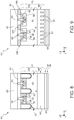
Figures 2-7 are cross-sectional views of the present MOSFET device in successive manufacturing steps; -
Figure 8 shows a different embodiment of the present vertical conduction power MOSFET device; -
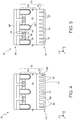
Figure 9 shows yet a further embodiment of the present vertical conduction power MOSFET device. - Described hereinafter are steps for manufacturing a vertical conduction power MOSFET device, which can be used in electronic apparatuses, especially apparatuses operating at low reference voltages.
- In particular, the manufacturing steps described below lead to the production of a MOSFET device having a general structure similar to the one illustrated in
Figure 1 . Consequently, the elements that are in common with the ones already described with reference toFigure 1 are designated by the same reference numbers increased by 50. - In detail,
Figure 2 is a cross-sectional view of awafer 50 of semiconductor material, for example of N-doped silicon, that has been processed in a way known to the person skilled in the art, for example in a way similar to what is described in the European patent application No.3396718 . In particular, in thewafer 50 there have already been provided thesubstrate 52 and the epitaxial layer 54 (which form thebody 70 having a first and asecond surface active regions 55, thesource regions 56, the first and secondenriched regions insulated-gate regions 59, thedrift region 60 and thedielectric insulation region 61. In addition, on the dielectric insulation region 61 ametal contact layer 48 has already been deposited, which fillscontact trenches 49 dug in the dielectric insulation region 61 (where it forms the metal contact regions 63) and has a surface portion 48' that extends over thedielectric insulation region 61 itself. - Furthermore, a
patterning layer 82, made, for example, of photosensitive material such as resist, has been deposited on thesecond surface 70B of thebody 70 and has been patterned via lithographic processes to form a plurality ofcavities 83, which have, for example, a circular cross-section with a diameter comprised between 0.5 µm and 3 µm, in particular between 1 µm and 2 µm. -
Figure 3 shows thewafer 50 following a chemical etching carried out on thesecond surface 70B of thebody 70. Chemical etching enables selective removal of portions of thesubstrate 52 at thecavities 83, thus forming a plurality oftrenches 84 that extend along the first axis Z for a high depth. For instance, for a substrate having a depth of 250 µm, thetrenches 84 may have a depth comprised between 150 µm and 250 µm; however, these values are not limiting, and thetrenches 84 may extend throughout the entire thickness of the substrate until reaching a minimum distance from theepitaxial layer 54, typically not less than 1 µm. Likewise, in the case of a thinner or thicker substrate, thetrenches 84 may extend only through part of thesubstrate 52 or until reaching a minimum distance from theepitaxial layer 54 of no less than 1 µm. - In particular, the fact that the
trenches 84 extend to a minimum distance from theepitaxial layer 54 helps ensuring that the thickness of theepitaxial layer 54 complies with the value defined at the design stage, and therefore it is not affected by the manufacturing steps that form thetrenches 84 or by the subsequent manufacturing steps. In fact, the minimum distance is evaluated at the design stage to take into account the process variabilities and tolerances of such manufacturing steps. - In practice, the
substrate 52 is now formed by the alternation oftrenches 84 andsemiconductor columns 81. - Formation of the
trenches 84 can be carried out by means of processes known to the person skilled in the art such as, stain etching, metal-assisted chemical etching and reactive-ion etching. - Next, as illustrated in
Figure 4 , thepatterning layer 82 is removed and ametal layer 85 of conductive material is deposited, for example a transition metal, such as titanium or tungsten if thesubstrate 52 has a doping of an N-type, or cobalt or chromium if thesubstrate 52 has a doping of a P-type. - The
metal layer 85 is deposited to completely fill thetrenches 84 and form a surface portion 85' that covers thesecond surface 70B of thebody 70. - In
Figure 5 , thewafer 50 is subjected to annealing, at a temperature comprised between 700°C and 900°C, for a time, which depends upon the temperature, comprised between 1 and 2 min. - The above thermal budget is sufficiently low not to affect the structures previously formed (
active regions 55,source regions 56, first and secondenriched regions 57, 58) but enables the portions ofsubstrate 52 in contact with themetal layer 85 to chemically react with themetal layer 85 itself, to form a highly conductive silicide. For instance, in the case where themetal layer 85 is of titanium, titanium silicide (TiSi2) is obtained. At the end of the annealing process, theentire substrate 52 has undergone the silicidation reaction. In this way, all the silicon of thesubstrate 52 has been transformed into silicide, while, in this embodiment, only part of themetal layer 85 in thetrenches 84 has been consumed, also this having been transformed into silicide. Thewafer 50 thus has, underneath theepitaxial layer 54, ametal drain layer 90 formed by silicide columns 91 (deriving from silicidation of thesemiconductor columns 81 and of part of the metal of the trenches 84), which surround columns of metal material 92 (remaining portion of themetal layer 85, not reacted into silicide). Alternatively, according to the metals used, the dimensions and the process parameters, all the metal present in thetrenches 84 may completely undergo the silicidation reaction, as shown hereinafter inFigure 8 . - The
metal drain layer 90 thus formed has a conductivity that is higher than that of the doped semiconductor material, for example N-doped silicon, of which thesubstrate 52 was made; this conductivity is also higher than in the case of a substrate having trenches filled with metal material surrounded by columns of semiconductor material, given that now the entire area of themetal drain layer 90 has an extremely high conductivity. In practice, the present solution enables a considerable reduction of the resistance Rs associated with thesubstrate 52, which now comprises a much larger surface with extremely low resistivity available for the flow of current. - Next,
Figure 6 , thewafer 50 undergoes chemical etching according to processes known to the person skilled in the art, for example anisotropic dry chemical etching, to remove the surface portion 48' of themetal contact layer 48. Afirst metallization layer 86, for example of aluminium, is then deposited on thedielectric insulation region 61 and on themetal contact regions 63, thus forming thesource terminal 62. - Finally,
Figure 7 , a second and athird metallization layer metal drain layer 90, to form thedrain terminal 53. Thesecond metallization layer 87, for example consisting of a compound of nickel and palladium or nickel and vanadium, favours the ohmic contact with theunderlying metal layer 85. Thethird metallization layer 88, made, for example of gold, silver or palladium, prevents oxidation of thefirst metallization layer 87. - The
wafer 50 is then diced, and each resulting die, after usual steps of electrical connection and packaging, forms aMOSFET device 51. - Thanks to the fact that the
substrate 52, now corresponding to themetal drain layer 90, consists completely of metal, as discussed above, thepresent MOSFET device 51 has a very low substrate resistance Rs, maintaining, at the same time, mechanical stability and low manufacturing costs. In fact, the manufacturing steps described above can easily be integrated in the process for manufacturing current power MOSFET devices and do not entail complex or costly manufacturing procedures. -
Figure 8 shows aMOSFET device 101 according to a further embodiment. TheMOSFET device 101 has undergone manufacturing steps similar to those of theMOSFET device 51 and thus has a similar structure; consequently, the elements that are in common are designated by the same reference numbers. Here, at the end of annealing, all the metal present in thetrenches 84 has reacted completely and also the area where the trenches were present is occupied by silicide. In practice, asilicide region 141 extends over theentire substrate 52 to form ametal drain layer 140, entirely consisting of silicide, arranged between theepitaxial layer 54 and thedrain terminal 53. It is evident that also in this case themetal drain layer 140 has a particularly low substrate resistance Rs since it is entirely made of material with extremely low resistivity. - Alternatively, a
MOSFET device 151 may be provided, as illustrated inFigure 9 . Also here, the elements that are in common with those of theMOSFET device 51 are designated by the same reference numbers. In this embodiment, thesemiconductor columns 81 ofFigure 4 have completely reacted with themetal layer 85 to formsilicide columns 91, while only part of thetrenches 84 have reacted to form the columns ofmetal material 92, in a way similar to what is illustrated inFigure 5 . Unlike theMOSFET device 51,insulated-gate regions 109 have been obtained, in a way known to the person skilled in the art, on top of theepitaxial layer 54 and within thedielectric insulation region 61. - Finally, it is clear that modifications and variations may be made to the
MOSFET device - For instance, the various embodiments described may be combined to provide further solutions.
- For example, the manufacturing process described above may be adjusted so that almost the
whole substrate 52 is transformed into silicide. In particular, the silicide columns or the silicide region may extend, along the first axis Z, from thesecond surface 70B of thebody 70 to a distance, for example of about 1 µm, from the interface between thesubstrate 52 and theepitaxial layer 54, which is much smaller than the thickness of thesubstrate 52 that has reacted into silicide. By virtue of this distance, the thickness of theepitaxial layer 54 may be unaffected by variabilities of the manufacturing process and therefore may comply with the value defined at the design stage. - Moreover, it is clear to the person skilled in the art that, in the
wafer 50, the interface between thesubstrate 52 and theepitaxial layer 54 may comprise a transition region, which extends along the first axis Z. In this transition region, the doping level varies between the doping level of thesubstrate 52 and the doping level of theepitaxial layer 54. Therefore, a boundary of thesubstrate 52, for example used to evaluate the thickness thereof, may be considered to lie where the doping level starts decreasing from the value of the doping level of thesubstrate 52. In this case, thetrenches 84 are formed to extend up to a minimum distance from the boundary of thesubstrate 52, so that thesilicide columns 91 or thesilicide region 141 do not extend within the transition region. - In addition, the manufacturing process described may be used for reducing the substrate resistance of other vertical conduction power devices, for example devices that have a different design of the insulated-gate regions, diodes such as a Triode for alternating current (Triac) or bipolar devices such as a thyristor, a Silicon Controlled Rectifier (SRC) or an Insulated-Gate Bipolar Transistor (IGBT), where it is necessary to have a resistance, of the current path between the two conduction terminals, that is as low as possible.
- Finally, the types of doping of the substrate, the epitaxial layer, the active regions, the source regions and the first and second enriched regions may be reversed.
Claims (13)
- A vertical conduction electronic power device (51, 101, 151) comprising:a body (70) having a first and a second surface (70A, 70B) and comprising an epitaxial layer (54), of semiconductor material, and a substrate (90; 140), the epitaxial layer being delimited by the first surface (70A) of the body and the substrate being delimited by the second surface (70B) of the body, the epitaxial layer housing at least a first and a second conduction region (56, 60) having a first conductivity type (N) and an active channel region (55) having a second conductivity type (P);a plurality of insulated-gate regions (59; 109), which extend over the first surface (70A) of the body (70) or within the epitaxial layer (54);wherein the substrate (90; 140) has at least one silicide region (91; 141), which extends from the second surface (70B) of the body (70) towards the epitaxial layer, wherein the substrate (140) is completely formed by the silicide region (141) or the substrate (90) is formed by a plurality of silicide regions (91), which include the at least one silicide region, extend from the second surface (70B) of the body (70) towards the epitaxial layer (54) and surround a plurality of metal regions (92).
- The device according to the preceding claim, wherein the at least one silicide region extends to the epitaxial layer.
- The device according to any one of the preceding claims, which forms a vertical conduction power transistor.
- The device according to any one of the preceding claims, further comprising: a first conduction terminal (62) superimposed on the first surface (70A) of the body (70) and in electrical contact with the first conduction region (56); and a second conduction terminal (53) superimposed on the second surface (70B) of the body (70) and in direct electrical contact with the at least one silicide region (91, 141).
- A method for manufacturing a vertical conduction electronic power device (51; 101; 151), starting from a wafer (50) of semiconductor material including an epitaxial layer (54) and a substrate (52) and having a first and a second surface (70A, 70B), the method comprising:forming a plurality of insulated-gate regions (59; 109) on the first surface (70A) of the wafer (50) or within the epitaxial layer;forming a first and a second conduction region (56, 60), of a first conductivity type, within the epitaxial layer;forming an active channel region (55), of a second conductivity type, within the epitaxial layer; andforming, in the substrate (52), at least one silicide region (91; 141), which extends from the second surface (70B) of the body (70) towards the epitaxial layer, thereby the substrate (140) is completely formed by the silicide region (141) or the substrate (90) is formed by a plurality of silicide regions (91), which include the at least one silicide region, extend from the second surface (70B) of the body (70) towards the epitaxial layer (54) and surround a plurality of metal regions (92).
- The method according to the preceding claim, wherein forming at least one silicide region comprises:forming trenches (84) in the substrate (52) starting from the second surface (70B) of the wafer (50), the trenches (84) being separated from one another by columns (81) of semiconductor material;filling the trenches (84) with filling regions (85) of metal material; andannealing the wafer (50) so that the semiconductor material of the columns (81) reacts with the metal material of the filling regions (85), to form at least one silicide region (91; 141).
- The method according to the preceding claim, wherein annealing is continued until all the semiconductor material of the columns (81) is transformed into silicide.
- The method according to claim 6 or 7, wherein annealing occurs at a temperature comprised between 700°C and 900°C for a time comprised between 1 min and 2 min.
- The method according to any one of the claims 6-8, wherein the substrate has a depth and the trenches extend approximately throughout the entire depth of the substrate, for example up to a distance of at least 1 µm from the epitaxial layer (54).
- The method according to the preceding claim, wherein the trenches (84) extend for a depth comprised between 150 µm and 250 µm and have a width comprised between 1 µm and 3 µm.
- The method according to any one of claims 5-10, further comprising forming a first metallization region (86) on the first surface (70A) and forming a second metallization region (87-88) on the second surface (70B), wherein forming at least one silicide region is carried out after forming the first and second conduction regions (56, 60) and prior to forming the first metallization region (86) and forming the second metallization region (87-88).
- The method according to any one of claims 6-11, wherein the substrate (52) has a doping of a N-type and the metal material of the filling regions (85) is a material chosen in the group comprising titanium and tungsten.
- The method according to any one of claims 6-11, wherein the substrate (52) has a doping of a P-type, and the metal material of the filling regions (85) is a material chosen in the group comprising cobalt or chromium.
Applications Claiming Priority (1)
| Application Number | Priority Date | Filing Date | Title |
|---|---|---|---|
| IT102020000001942A IT202000001942A1 (en) | 2020-01-31 | 2020-01-31 | ELECTRONIC POWER DEVICE WITH VERTICAL CONDUCTION WITH REDUCED IGNITION RESISTANCE AND RELATED MANUFACTURING PROCESS |
Publications (2)
| Publication Number | Publication Date |
|---|---|
| EP3859789A1 true EP3859789A1 (en) | 2021-08-04 |
| EP3859789B1 EP3859789B1 (en) | 2023-12-27 |
Family
ID=70228718
Family Applications (1)
| Application Number | Title | Priority Date | Filing Date |
|---|---|---|---|
| EP21154045.5A Active EP3859789B1 (en) | 2020-01-31 | 2021-01-28 | Vertical conduction electronic power device having a reduced on resistance and manufacturing process thereof |
Country Status (4)
| Country | Link |
|---|---|
| US (1) | US12046655B2 (en) |
| EP (1) | EP3859789B1 (en) |
| CN (2) | CN113206154B (en) |
| IT (1) | IT202000001942A1 (en) |
Families Citing this family (3)
| Publication number | Priority date | Publication date | Assignee | Title |
|---|---|---|---|---|
| IT201800007780A1 (en) | 2018-08-02 | 2020-02-02 | St Microelectronics Srl | SILICON CARBIDE MOSFET DEVICE AND ITS MANUFACTURING METHOD |
| IT202000001942A1 (en) * | 2020-01-31 | 2021-07-31 | St Microelectronics Srl | ELECTRONIC POWER DEVICE WITH VERTICAL CONDUCTION WITH REDUCED IGNITION RESISTANCE AND RELATED MANUFACTURING PROCESS |
| CN113990933B (en) * | 2021-10-28 | 2023-05-26 | 电子科技大学 | Semiconductor longitudinal device and preparation method thereof |
Citations (6)
| Publication number | Priority date | Publication date | Assignee | Title |
|---|---|---|---|---|
| US20020197832A1 (en) | 2001-06-08 | 2002-12-26 | Volker Lehmann | Method for fabricating a semiconductor component and semiconductor component |
| US20070272980A1 (en) * | 2006-05-05 | 2007-11-29 | Angelo Magri | Semiconductor device with vertical current flow and low substrate resistance and manufacturing process thereof |
| US20120313162A1 (en) | 2011-06-10 | 2012-12-13 | Kabushiki Kaisha Toshiba | Semiconductor device, method for manufacturing metal film, and method for manufacturing semiconductor device |
| US20140048904A1 (en) | 2012-08-20 | 2014-02-20 | Infineon Technologies Ag | Semiconductor Device, Integrated Circuit and Manufacturing Method Thereof |
| US20160372572A1 (en) | 2014-12-04 | 2016-12-22 | Shuk-Wa FUNG | Trench gate power semiconductor field effect transistor |
| EP3396718A1 (en) | 2017-04-28 | 2018-10-31 | STMicroelectronics S.r.l. | Power mos device having an integrated current sensor and manufacturing process thereof |
Family Cites Families (7)
| Publication number | Priority date | Publication date | Assignee | Title |
|---|---|---|---|---|
| JP5121475B2 (en) * | 2008-01-28 | 2013-01-16 | 株式会社東芝 | Semiconductor memory device |
| JP5995435B2 (en) * | 2011-08-02 | 2016-09-21 | ローム株式会社 | Semiconductor device and manufacturing method thereof |
| JP5728339B2 (en) * | 2011-09-08 | 2015-06-03 | 株式会社東芝 | Semiconductor device and manufacturing method of semiconductor device |
| JP2015041638A (en) * | 2013-08-20 | 2015-03-02 | 住友電気工業株式会社 | Silicon carbide semiconductor device and manufacturing method thereof |
| CN105448981A (en) * | 2014-06-20 | 2016-03-30 | 北大方正集团有限公司 | VDMOS device, drain electrode structure thereof, and manufacturing method |
| JP7225873B2 (en) * | 2019-02-07 | 2023-02-21 | 富士電機株式会社 | Semiconductor device and method for manufacturing semiconductor device |
| IT202000001942A1 (en) * | 2020-01-31 | 2021-07-31 | St Microelectronics Srl | ELECTRONIC POWER DEVICE WITH VERTICAL CONDUCTION WITH REDUCED IGNITION RESISTANCE AND RELATED MANUFACTURING PROCESS |
-
2020
- 2020-01-31 IT IT102020000001942A patent/IT202000001942A1/en unknown
-
2021
- 2021-01-28 EP EP21154045.5A patent/EP3859789B1/en active Active
- 2021-01-28 US US17/161,059 patent/US12046655B2/en active Active
- 2021-02-01 CN CN202110139503.7A patent/CN113206154B/en active Active
- 2021-02-01 CN CN202120281925.3U patent/CN214588867U/en active Active
Patent Citations (6)
| Publication number | Priority date | Publication date | Assignee | Title |
|---|---|---|---|---|
| US20020197832A1 (en) | 2001-06-08 | 2002-12-26 | Volker Lehmann | Method for fabricating a semiconductor component and semiconductor component |
| US20070272980A1 (en) * | 2006-05-05 | 2007-11-29 | Angelo Magri | Semiconductor device with vertical current flow and low substrate resistance and manufacturing process thereof |
| US20120313162A1 (en) | 2011-06-10 | 2012-12-13 | Kabushiki Kaisha Toshiba | Semiconductor device, method for manufacturing metal film, and method for manufacturing semiconductor device |
| US20140048904A1 (en) | 2012-08-20 | 2014-02-20 | Infineon Technologies Ag | Semiconductor Device, Integrated Circuit and Manufacturing Method Thereof |
| US20160372572A1 (en) | 2014-12-04 | 2016-12-22 | Shuk-Wa FUNG | Trench gate power semiconductor field effect transistor |
| EP3396718A1 (en) | 2017-04-28 | 2018-10-31 | STMicroelectronics S.r.l. | Power mos device having an integrated current sensor and manufacturing process thereof |
Also Published As
| Publication number | Publication date |
|---|---|
| US20210242323A1 (en) | 2021-08-05 |
| US12046655B2 (en) | 2024-07-23 |
| CN113206154A (en) | 2021-08-03 |
| EP3859789B1 (en) | 2023-12-27 |
| IT202000001942A1 (en) | 2021-07-31 |
| CN113206154B (en) | 2025-10-17 |
| CN214588867U (en) | 2021-11-02 |
Similar Documents
| Publication | Publication Date | Title |
|---|---|---|
| KR101729935B1 (en) | Method of forming an insulated gate field effect transistor device having a shield electrode structure | |
| CN102856182B (en) | Manufacture method and the structure of Iusulated gate semiconductor device | |
| KR101728741B1 (en) | Method of forming an insulated gate field effect transistor device having a shield electrode structure | |
| CN103426771B (en) | The method of insulated gate semiconductor device of the manufacture with shield electrode structure | |
| US9837358B2 (en) | Source-gate region architecture in a vertical power semiconductor device | |
| EP3859789B1 (en) | Vertical conduction electronic power device having a reduced on resistance and manufacturing process thereof | |
| CN114725202A (en) | Semiconductor device | |
| US10128368B2 (en) | Double gate trench power transistor and manufacturing method thereof | |
| CN107910269B (en) | Power semiconductor device and method of manufacturing the same | |
| CN107910266A (en) | Power semiconductor and its manufacture method | |
| CN107910268B (en) | Power semiconductor device and method of manufacturing the same | |
| US8987820B1 (en) | Lateral double diffused metal-oxide-semiconductor device and method for fabricating the same | |
| KR102500888B1 (en) | Split Gate Power MOSFET and Method for Manufacturing The Same | |
| CN107910271A (en) | Power semiconductor and its manufacture method | |
| US20120119381A1 (en) | Semiconductor device with vertical current flow and low substrate resistance and manufacturing process thereof | |
| JP2026050161A (en) | Semiconductor device and method for manufacturing the same | |
| CN120730806A (en) | Reverse conducting IGBT device with low efficiency injection anode and manufacturing process thereof | |
| CN119325257A (en) | Self-aligned buried gate metal MOSFET and method of manufacture | |
| HK1191444A (en) | Method of making an insulated gate semiconductor device having a shield electrode structure | |
| HK1144493A1 (en) | Contact structure for semiconductor device having trench shield electrode and method | |
| HK1157934B (en) | Method of forming an insulated gate field effect transistor device having a shield electrode structure | |
| HK1144493B (en) | Contact structure for semiconductor device having trench shield electrode and method | |
| HK1191444B (en) | Method of making an insulated gate semiconductor device having a shield electrode structure | |
| HK1144494A (en) | Trench shielding structure for semiconductor device and method | |
| HK1144494B (en) | Trench shielding structure for semiconductor device and method |
Legal Events
| Date | Code | Title | Description |
|---|---|---|---|
| PUAI | Public reference made under article 153(3) epc to a published international application that has entered the european phase |
Free format text: ORIGINAL CODE: 0009012 |
|
| STAA | Information on the status of an ep patent application or granted ep patent |
Free format text: STATUS: THE APPLICATION HAS BEEN PUBLISHED |
|
| AK | Designated contracting states |
Kind code of ref document: A1 Designated state(s): AL AT BE BG CH CY CZ DE DK EE ES FI FR GB GR HR HU IE IS IT LI LT LU LV MC MK MT NL NO PL PT RO RS SE SI SK SM TR |
|
| STAA | Information on the status of an ep patent application or granted ep patent |
Free format text: STATUS: REQUEST FOR EXAMINATION WAS MADE |
|
| 17P | Request for examination filed |
Effective date: 20220202 |
|
| RBV | Designated contracting states (corrected) |
Designated state(s): AL AT BE BG CH CY CZ DE DK EE ES FI FR GB GR HR HU IE IS IT LI LT LU LV MC MK MT NL NO PL PT RO RS SE SI SK SM TR |
|
| GRAP | Despatch of communication of intention to grant a patent |
Free format text: ORIGINAL CODE: EPIDOSNIGR1 |
|
| STAA | Information on the status of an ep patent application or granted ep patent |
Free format text: STATUS: GRANT OF PATENT IS INTENDED |
|
| INTG | Intention to grant announced |
Effective date: 20230719 |
|
| GRAS | Grant fee paid |
Free format text: ORIGINAL CODE: EPIDOSNIGR3 |
|
| GRAA | (expected) grant |
Free format text: ORIGINAL CODE: 0009210 |
|
| STAA | Information on the status of an ep patent application or granted ep patent |
Free format text: STATUS: THE PATENT HAS BEEN GRANTED |
|
| AK | Designated contracting states |
Kind code of ref document: B1 Designated state(s): AL AT BE BG CH CY CZ DE DK EE ES FI FR GB GR HR HU IE IS IT LI LT LU LV MC MK MT NL NO PL PT RO RS SE SI SK SM TR |
|
| REG | Reference to a national code |
Ref country code: GB Ref legal event code: FG4D |
|
| REG | Reference to a national code |
Ref country code: CH Ref legal event code: EP |
|
| REG | Reference to a national code |
Ref country code: DE Ref legal event code: R096 Ref document number: 602021007960 Country of ref document: DE |
|
| REG | Reference to a national code |
Ref country code: IE Ref legal event code: FG4D |
|
| PG25 | Lapsed in a contracting state [announced via postgrant information from national office to epo] |
Ref country code: GR Free format text: LAPSE BECAUSE OF FAILURE TO SUBMIT A TRANSLATION OF THE DESCRIPTION OR TO PAY THE FEE WITHIN THE PRESCRIBED TIME-LIMIT Effective date: 20240328 |
|
| REG | Reference to a national code |
Ref country code: LT Ref legal event code: MG9D |
|
| PG25 | Lapsed in a contracting state [announced via postgrant information from national office to epo] |
Ref country code: LT Free format text: LAPSE BECAUSE OF FAILURE TO SUBMIT A TRANSLATION OF THE DESCRIPTION OR TO PAY THE FEE WITHIN THE PRESCRIBED TIME-LIMIT Effective date: 20231227 |
|
| PG25 | Lapsed in a contracting state [announced via postgrant information from national office to epo] |
Ref country code: ES Free format text: LAPSE BECAUSE OF FAILURE TO SUBMIT A TRANSLATION OF THE DESCRIPTION OR TO PAY THE FEE WITHIN THE PRESCRIBED TIME-LIMIT Effective date: 20231227 |
|
| PG25 | Lapsed in a contracting state [announced via postgrant information from national office to epo] |
Ref country code: LT Free format text: LAPSE BECAUSE OF FAILURE TO SUBMIT A TRANSLATION OF THE DESCRIPTION OR TO PAY THE FEE WITHIN THE PRESCRIBED TIME-LIMIT Effective date: 20231227 Ref country code: GR Free format text: LAPSE BECAUSE OF FAILURE TO SUBMIT A TRANSLATION OF THE DESCRIPTION OR TO PAY THE FEE WITHIN THE PRESCRIBED TIME-LIMIT Effective date: 20240328 Ref country code: FI Free format text: LAPSE BECAUSE OF FAILURE TO SUBMIT A TRANSLATION OF THE DESCRIPTION OR TO PAY THE FEE WITHIN THE PRESCRIBED TIME-LIMIT Effective date: 20231227 Ref country code: ES Free format text: LAPSE BECAUSE OF FAILURE TO SUBMIT A TRANSLATION OF THE DESCRIPTION OR TO PAY THE FEE WITHIN THE PRESCRIBED TIME-LIMIT Effective date: 20231227 Ref country code: BG Free format text: LAPSE BECAUSE OF FAILURE TO SUBMIT A TRANSLATION OF THE DESCRIPTION OR TO PAY THE FEE WITHIN THE PRESCRIBED TIME-LIMIT Effective date: 20240327 |
|
| REG | Reference to a national code |
Ref country code: NL Ref legal event code: MP Effective date: 20231227 |
|
| REG | Reference to a national code |
Ref country code: AT Ref legal event code: MK05 Ref document number: 1645367 Country of ref document: AT Kind code of ref document: T Effective date: 20231227 |
|
| PG25 | Lapsed in a contracting state [announced via postgrant information from national office to epo] |
Ref country code: NL Free format text: LAPSE BECAUSE OF FAILURE TO SUBMIT A TRANSLATION OF THE DESCRIPTION OR TO PAY THE FEE WITHIN THE PRESCRIBED TIME-LIMIT Effective date: 20231227 |
|
| PG25 | Lapsed in a contracting state [announced via postgrant information from national office to epo] |
Ref country code: SE Free format text: LAPSE BECAUSE OF FAILURE TO SUBMIT A TRANSLATION OF THE DESCRIPTION OR TO PAY THE FEE WITHIN THE PRESCRIBED TIME-LIMIT Effective date: 20231227 Ref country code: RS Free format text: LAPSE BECAUSE OF FAILURE TO SUBMIT A TRANSLATION OF THE DESCRIPTION OR TO PAY THE FEE WITHIN THE PRESCRIBED TIME-LIMIT Effective date: 20231227 Ref country code: NO Free format text: LAPSE BECAUSE OF FAILURE TO SUBMIT A TRANSLATION OF THE DESCRIPTION OR TO PAY THE FEE WITHIN THE PRESCRIBED TIME-LIMIT Effective date: 20240327 Ref country code: NL Free format text: LAPSE BECAUSE OF FAILURE TO SUBMIT A TRANSLATION OF THE DESCRIPTION OR TO PAY THE FEE WITHIN THE PRESCRIBED TIME-LIMIT Effective date: 20231227 Ref country code: LV Free format text: LAPSE BECAUSE OF FAILURE TO SUBMIT A TRANSLATION OF THE DESCRIPTION OR TO PAY THE FEE WITHIN THE PRESCRIBED TIME-LIMIT Effective date: 20231227 Ref country code: HR Free format text: LAPSE BECAUSE OF FAILURE TO SUBMIT A TRANSLATION OF THE DESCRIPTION OR TO PAY THE FEE WITHIN THE PRESCRIBED TIME-LIMIT Effective date: 20231227 |
|
| PG25 | Lapsed in a contracting state [announced via postgrant information from national office to epo] |
Ref country code: IS Free format text: LAPSE BECAUSE OF FAILURE TO SUBMIT A TRANSLATION OF THE DESCRIPTION OR TO PAY THE FEE WITHIN THE PRESCRIBED TIME-LIMIT Effective date: 20240427 |
|
| PG25 | Lapsed in a contracting state [announced via postgrant information from national office to epo] |
Ref country code: CZ Free format text: LAPSE BECAUSE OF FAILURE TO SUBMIT A TRANSLATION OF THE DESCRIPTION OR TO PAY THE FEE WITHIN THE PRESCRIBED TIME-LIMIT Effective date: 20231227 Ref country code: AT Free format text: LAPSE BECAUSE OF FAILURE TO SUBMIT A TRANSLATION OF THE DESCRIPTION OR TO PAY THE FEE WITHIN THE PRESCRIBED TIME-LIMIT Effective date: 20231227 |
|
| PG25 | Lapsed in a contracting state [announced via postgrant information from national office to epo] |
Ref country code: SK Free format text: LAPSE BECAUSE OF FAILURE TO SUBMIT A TRANSLATION OF THE DESCRIPTION OR TO PAY THE FEE WITHIN THE PRESCRIBED TIME-LIMIT Effective date: 20231227 |
|
| PG25 | Lapsed in a contracting state [announced via postgrant information from national office to epo] |
Ref country code: SM Free format text: LAPSE BECAUSE OF FAILURE TO SUBMIT A TRANSLATION OF THE DESCRIPTION OR TO PAY THE FEE WITHIN THE PRESCRIBED TIME-LIMIT Effective date: 20231227 Ref country code: SK Free format text: LAPSE BECAUSE OF FAILURE TO SUBMIT A TRANSLATION OF THE DESCRIPTION OR TO PAY THE FEE WITHIN THE PRESCRIBED TIME-LIMIT Effective date: 20231227 Ref country code: RO Free format text: LAPSE BECAUSE OF FAILURE TO SUBMIT A TRANSLATION OF THE DESCRIPTION OR TO PAY THE FEE WITHIN THE PRESCRIBED TIME-LIMIT Effective date: 20231227 Ref country code: IT Free format text: LAPSE BECAUSE OF FAILURE TO SUBMIT A TRANSLATION OF THE DESCRIPTION OR TO PAY THE FEE WITHIN THE PRESCRIBED TIME-LIMIT Effective date: 20231227 Ref country code: IS Free format text: LAPSE BECAUSE OF FAILURE TO SUBMIT A TRANSLATION OF THE DESCRIPTION OR TO PAY THE FEE WITHIN THE PRESCRIBED TIME-LIMIT Effective date: 20240427 Ref country code: EE Free format text: LAPSE BECAUSE OF FAILURE TO SUBMIT A TRANSLATION OF THE DESCRIPTION OR TO PAY THE FEE WITHIN THE PRESCRIBED TIME-LIMIT Effective date: 20231227 Ref country code: CZ Free format text: LAPSE BECAUSE OF FAILURE TO SUBMIT A TRANSLATION OF THE DESCRIPTION OR TO PAY THE FEE WITHIN THE PRESCRIBED TIME-LIMIT Effective date: 20231227 Ref country code: AT Free format text: LAPSE BECAUSE OF FAILURE TO SUBMIT A TRANSLATION OF THE DESCRIPTION OR TO PAY THE FEE WITHIN THE PRESCRIBED TIME-LIMIT Effective date: 20231227 |
|
| PG25 | Lapsed in a contracting state [announced via postgrant information from national office to epo] |
Ref country code: PL Free format text: LAPSE BECAUSE OF FAILURE TO SUBMIT A TRANSLATION OF THE DESCRIPTION OR TO PAY THE FEE WITHIN THE PRESCRIBED TIME-LIMIT Effective date: 20231227 Ref country code: PT Free format text: LAPSE BECAUSE OF FAILURE TO SUBMIT A TRANSLATION OF THE DESCRIPTION OR TO PAY THE FEE WITHIN THE PRESCRIBED TIME-LIMIT Effective date: 20240429 |
|
| PG25 | Lapsed in a contracting state [announced via postgrant information from national office to epo] |
Ref country code: PT Free format text: LAPSE BECAUSE OF FAILURE TO SUBMIT A TRANSLATION OF THE DESCRIPTION OR TO PAY THE FEE WITHIN THE PRESCRIBED TIME-LIMIT Effective date: 20240429 Ref country code: PL Free format text: LAPSE BECAUSE OF FAILURE TO SUBMIT A TRANSLATION OF THE DESCRIPTION OR TO PAY THE FEE WITHIN THE PRESCRIBED TIME-LIMIT Effective date: 20231227 |
|
| REG | Reference to a national code |
Ref country code: CH Ref legal event code: PL |
|
| PG25 | Lapsed in a contracting state [announced via postgrant information from national office to epo] |
Ref country code: LU Free format text: LAPSE BECAUSE OF NON-PAYMENT OF DUE FEES Effective date: 20240128 |
|
| PG25 | Lapsed in a contracting state [announced via postgrant information from national office to epo] |
Ref country code: LU Free format text: LAPSE BECAUSE OF NON-PAYMENT OF DUE FEES Effective date: 20240128 Ref country code: MC Free format text: LAPSE BECAUSE OF FAILURE TO SUBMIT A TRANSLATION OF THE DESCRIPTION OR TO PAY THE FEE WITHIN THE PRESCRIBED TIME-LIMIT Effective date: 20231227 |
|
| REG | Reference to a national code |
Ref country code: DE Ref legal event code: R097 Ref document number: 602021007960 Country of ref document: DE |
|
| PG25 | Lapsed in a contracting state [announced via postgrant information from national office to epo] |
Ref country code: DK Free format text: LAPSE BECAUSE OF FAILURE TO SUBMIT A TRANSLATION OF THE DESCRIPTION OR TO PAY THE FEE WITHIN THE PRESCRIBED TIME-LIMIT Effective date: 20231227 |
|
| PG25 | Lapsed in a contracting state [announced via postgrant information from national office to epo] |
Ref country code: BE Free format text: LAPSE BECAUSE OF NON-PAYMENT OF DUE FEES Effective date: 20240131 |
|
| PG25 | Lapsed in a contracting state [announced via postgrant information from national office to epo] |
Ref country code: CH Free format text: LAPSE BECAUSE OF NON-PAYMENT OF DUE FEES Effective date: 20240131 |
|
| PG25 | Lapsed in a contracting state [announced via postgrant information from national office to epo] |
Ref country code: DK Free format text: LAPSE BECAUSE OF FAILURE TO SUBMIT A TRANSLATION OF THE DESCRIPTION OR TO PAY THE FEE WITHIN THE PRESCRIBED TIME-LIMIT Effective date: 20231227 Ref country code: CH Free format text: LAPSE BECAUSE OF NON-PAYMENT OF DUE FEES Effective date: 20240131 Ref country code: BE Free format text: LAPSE BECAUSE OF NON-PAYMENT OF DUE FEES Effective date: 20240131 |
|
| PLBE | No opposition filed within time limit |
Free format text: ORIGINAL CODE: 0009261 |
|
| STAA | Information on the status of an ep patent application or granted ep patent |
Free format text: STATUS: NO OPPOSITION FILED WITHIN TIME LIMIT |
|
| REG | Reference to a national code |
Ref country code: BE Ref legal event code: MM Effective date: 20240131 |
|
| REG | Reference to a national code |
Ref country code: DE Ref legal event code: R079 Ref document number: 602021007960 Country of ref document: DE Free format text: PREVIOUS MAIN CLASS: H01L0029780000 Ipc: H10D0030600000 |
|
| 26N | No opposition filed |
Effective date: 20240930 |
|
| PG25 | Lapsed in a contracting state [announced via postgrant information from national office to epo] |
Ref country code: FR Free format text: LAPSE BECAUSE OF NON-PAYMENT OF DUE FEES Effective date: 20240227 |
|
| PG25 | Lapsed in a contracting state [announced via postgrant information from national office to epo] |
Ref country code: IE Free format text: LAPSE BECAUSE OF NON-PAYMENT OF DUE FEES Effective date: 20240128 |
|
| PG25 | Lapsed in a contracting state [announced via postgrant information from national office to epo] |
Ref country code: IE Free format text: LAPSE BECAUSE OF NON-PAYMENT OF DUE FEES Effective date: 20240128 Ref country code: FR Free format text: LAPSE BECAUSE OF NON-PAYMENT OF DUE FEES Effective date: 20240227 |
|
| PG25 | Lapsed in a contracting state [announced via postgrant information from national office to epo] |
Ref country code: SI Free format text: LAPSE BECAUSE OF FAILURE TO SUBMIT A TRANSLATION OF THE DESCRIPTION OR TO PAY THE FEE WITHIN THE PRESCRIBED TIME-LIMIT Effective date: 20231227 |
|
| PG25 | Lapsed in a contracting state [announced via postgrant information from national office to epo] |
Ref country code: CY Free format text: LAPSE BECAUSE OF FAILURE TO SUBMIT A TRANSLATION OF THE DESCRIPTION OR TO PAY THE FEE WITHIN THE PRESCRIBED TIME-LIMIT; INVALID AB INITIO Effective date: 20210128 |
|
| PG25 | Lapsed in a contracting state [announced via postgrant information from national office to epo] |
Ref country code: HU Free format text: LAPSE BECAUSE OF FAILURE TO SUBMIT A TRANSLATION OF THE DESCRIPTION OR TO PAY THE FEE WITHIN THE PRESCRIBED TIME-LIMIT; INVALID AB INITIO Effective date: 20210128 |
|
| GBPC | Gb: european patent ceased through non-payment of renewal fee |
Effective date: 20250128 |
|
| PG25 | Lapsed in a contracting state [announced via postgrant information from national office to epo] |
Ref country code: GB Free format text: LAPSE BECAUSE OF NON-PAYMENT OF DUE FEES Effective date: 20250128 |
|
| PG25 | Lapsed in a contracting state [announced via postgrant information from national office to epo] |
Ref country code: TR Free format text: LAPSE BECAUSE OF FAILURE TO SUBMIT A TRANSLATION OF THE DESCRIPTION OR TO PAY THE FEE WITHIN THE PRESCRIBED TIME-LIMIT Effective date: 20231227 |
|
| PGFP | Annual fee paid to national office [announced via postgrant information from national office to epo] |
Ref country code: DE Payment date: 20251217 Year of fee payment: 6 |