EP3396718A1 - Power mos device having an integrated current sensor and manufacturing process thereof - Google Patents
Power mos device having an integrated current sensor and manufacturing process thereof Download PDFInfo
- Publication number
- EP3396718A1 EP3396718A1 EP18168154.5A EP18168154A EP3396718A1 EP 3396718 A1 EP3396718 A1 EP 3396718A1 EP 18168154 A EP18168154 A EP 18168154A EP 3396718 A1 EP3396718 A1 EP 3396718A1
- Authority
- EP
- European Patent Office
- Prior art keywords
- region
- detection
- mos transistor
- insulated gate
- node
- Prior art date
- Legal status (The legal status is an assumption and is not a legal conclusion. Google has not performed a legal analysis and makes no representation as to the accuracy of the status listed.)
- Granted
Links
Images




Classifications
-
- H—ELECTRICITY
- H10—SEMICONDUCTOR DEVICES; ELECTRIC SOLID-STATE DEVICES NOT OTHERWISE PROVIDED FOR
- H10D—INORGANIC ELECTRIC SEMICONDUCTOR DEVICES
- H10D89/00—Aspects of integrated devices not covered by groups H10D84/00 - H10D88/00
- H10D89/60—Integrated devices comprising arrangements for electrical or thermal protection, e.g. protection circuits against electrostatic discharge [ESD]
- H10D89/601—Integrated devices comprising arrangements for electrical or thermal protection, e.g. protection circuits against electrostatic discharge [ESD] for devices having insulated gate electrodes, e.g. for IGFETs or IGBTs
-
- H—ELECTRICITY
- H10—SEMICONDUCTOR DEVICES; ELECTRIC SOLID-STATE DEVICES NOT OTHERWISE PROVIDED FOR
- H10D—INORGANIC ELECTRIC SEMICONDUCTOR DEVICES
- H10D89/00—Aspects of integrated devices not covered by groups H10D84/00 - H10D88/00
-
- H—ELECTRICITY
- H10—SEMICONDUCTOR DEVICES; ELECTRIC SOLID-STATE DEVICES NOT OTHERWISE PROVIDED FOR
- H10D—INORGANIC ELECTRIC SEMICONDUCTOR DEVICES
- H10D30/00—Field-effect transistors [FET]
- H10D30/01—Manufacture or treatment
- H10D30/021—Manufacture or treatment of FETs having insulated gates [IGFET]
-
- H—ELECTRICITY
- H10—SEMICONDUCTOR DEVICES; ELECTRIC SOLID-STATE DEVICES NOT OTHERWISE PROVIDED FOR
- H10D—INORGANIC ELECTRIC SEMICONDUCTOR DEVICES
- H10D30/00—Field-effect transistors [FET]
- H10D30/01—Manufacture or treatment
- H10D30/021—Manufacture or treatment of FETs having insulated gates [IGFET]
- H10D30/028—Manufacture or treatment of FETs having insulated gates [IGFET] of double-diffused metal oxide semiconductor [DMOS] FETs
- H10D30/0291—Manufacture or treatment of FETs having insulated gates [IGFET] of double-diffused metal oxide semiconductor [DMOS] FETs of vertical DMOS [VDMOS] FETs
- H10D30/0297—Manufacture or treatment of FETs having insulated gates [IGFET] of double-diffused metal oxide semiconductor [DMOS] FETs of vertical DMOS [VDMOS] FETs using recessing of the gate electrodes, e.g. to form trench gate electrodes
-
- H—ELECTRICITY
- H10—SEMICONDUCTOR DEVICES; ELECTRIC SOLID-STATE DEVICES NOT OTHERWISE PROVIDED FOR
- H10D—INORGANIC ELECTRIC SEMICONDUCTOR DEVICES
- H10D30/00—Field-effect transistors [FET]
- H10D30/60—Insulated-gate field-effect transistors [IGFET]
- H10D30/64—Double-diffused metal-oxide semiconductor [DMOS] FETs
- H10D30/66—Vertical DMOS [VDMOS] FETs
- H10D30/668—Vertical DMOS [VDMOS] FETs having trench gate electrodes, e.g. UMOS transistors
-
- H—ELECTRICITY
- H10—SEMICONDUCTOR DEVICES; ELECTRIC SOLID-STATE DEVICES NOT OTHERWISE PROVIDED FOR
- H10D—INORGANIC ELECTRIC SEMICONDUCTOR DEVICES
- H10D30/00—Field-effect transistors [FET]
- H10D30/60—Insulated-gate field-effect transistors [IGFET]
- H10D30/64—Double-diffused metal-oxide semiconductor [DMOS] FETs
- H10D30/66—Vertical DMOS [VDMOS] FETs
- H10D30/669—Vertical DMOS [VDMOS] FETs having voltage-sensing or current-sensing structures, e.g. emulator sections or overcurrent sensing cells
-
- H—ELECTRICITY
- H10—SEMICONDUCTOR DEVICES; ELECTRIC SOLID-STATE DEVICES NOT OTHERWISE PROVIDED FOR
- H10D—INORGANIC ELECTRIC SEMICONDUCTOR DEVICES
- H10D62/00—Semiconductor bodies, or regions thereof, of devices having potential barriers
- H10D62/10—Shapes, relative sizes or dispositions of the regions of the semiconductor bodies; Shapes of the semiconductor bodies
-
- H—ELECTRICITY
- H10—SEMICONDUCTOR DEVICES; ELECTRIC SOLID-STATE DEVICES NOT OTHERWISE PROVIDED FOR
- H10D—INORGANIC ELECTRIC SEMICONDUCTOR DEVICES
- H10D62/00—Semiconductor bodies, or regions thereof, of devices having potential barriers
- H10D62/10—Shapes, relative sizes or dispositions of the regions of the semiconductor bodies; Shapes of the semiconductor bodies
- H10D62/124—Shapes, relative sizes or dispositions of the regions of semiconductor bodies or of junctions between the regions
-
- H—ELECTRICITY
- H10—SEMICONDUCTOR DEVICES; ELECTRIC SOLID-STATE DEVICES NOT OTHERWISE PROVIDED FOR
- H10D—INORGANIC ELECTRIC SEMICONDUCTOR DEVICES
- H10D62/00—Semiconductor bodies, or regions thereof, of devices having potential barriers
- H10D62/10—Shapes, relative sizes or dispositions of the regions of the semiconductor bodies; Shapes of the semiconductor bodies
- H10D62/17—Semiconductor regions connected to electrodes not carrying current to be rectified, amplified or switched, e.g. channel regions
- H10D62/393—Body regions of DMOS transistors or IGBTs
-
- H—ELECTRICITY
- H10—SEMICONDUCTOR DEVICES; ELECTRIC SOLID-STATE DEVICES NOT OTHERWISE PROVIDED FOR
- H10D—INORGANIC ELECTRIC SEMICONDUCTOR DEVICES
- H10D64/00—Electrodes of devices having potential barriers
- H10D64/20—Electrodes characterised by their shapes, relative sizes or dispositions
- H10D64/23—Electrodes carrying the current to be rectified, amplified, oscillated or switched, e.g. sources, drains, anodes or cathodes
- H10D64/251—Source or drain electrodes for field-effect devices
- H10D64/256—Source or drain electrodes for field-effect devices for lateral devices wherein the source or drain electrodes are recessed in semiconductor bodies
-
- H—ELECTRICITY
- H10—SEMICONDUCTOR DEVICES; ELECTRIC SOLID-STATE DEVICES NOT OTHERWISE PROVIDED FOR
- H10D—INORGANIC ELECTRIC SEMICONDUCTOR DEVICES
- H10D84/00—Integrated devices formed in or on semiconductor substrates that comprise only semiconducting layers, e.g. on Si wafers or on GaAs-on-Si wafers
- H10D84/101—Integrated devices comprising main components and built-in components, e.g. IGBT having built-in freewheel diode
- H10D84/141—VDMOS having built-in components
-
- H—ELECTRICITY
- H10—SEMICONDUCTOR DEVICES; ELECTRIC SOLID-STATE DEVICES NOT OTHERWISE PROVIDED FOR
- H10D—INORGANIC ELECTRIC SEMICONDUCTOR DEVICES
- H10D84/00—Integrated devices formed in or on semiconductor substrates that comprise only semiconducting layers, e.g. on Si wafers or on GaAs-on-Si wafers
- H10D84/80—Integrated devices formed in or on semiconductor substrates that comprise only semiconducting layers, e.g. on Si wafers or on GaAs-on-Si wafers characterised by the integration of at least one component covered by groups H10D12/00 or H10D30/00, e.g. integration of IGFETs
- H10D84/811—Combinations of field-effect devices and one or more diodes, capacitors or resistors
-
- H—ELECTRICITY
- H10—SEMICONDUCTOR DEVICES; ELECTRIC SOLID-STATE DEVICES NOT OTHERWISE PROVIDED FOR
- H10D—INORGANIC ELECTRIC SEMICONDUCTOR DEVICES
- H10D30/00—Field-effect transistors [FET]
- H10D30/01—Manufacture or treatment
- H10D30/021—Manufacture or treatment of FETs having insulated gates [IGFET]
- H10D30/028—Manufacture or treatment of FETs having insulated gates [IGFET] of double-diffused metal oxide semiconductor [DMOS] FETs
- H10D30/0281—Manufacture or treatment of FETs having insulated gates [IGFET] of double-diffused metal oxide semiconductor [DMOS] FETs of lateral DMOS [LDMOS] FETs
- H10D30/0287—Manufacture or treatment of FETs having insulated gates [IGFET] of double-diffused metal oxide semiconductor [DMOS] FETs of lateral DMOS [LDMOS] FETs using recessing of the source electrodes
-
- H—ELECTRICITY
- H10—SEMICONDUCTOR DEVICES; ELECTRIC SOLID-STATE DEVICES NOT OTHERWISE PROVIDED FOR
- H10D—INORGANIC ELECTRIC SEMICONDUCTOR DEVICES
- H10D30/00—Field-effect transistors [FET]
- H10D30/60—Insulated-gate field-effect transistors [IGFET]
- H10D30/64—Double-diffused metal-oxide semiconductor [DMOS] FETs
- H10D30/66—Vertical DMOS [VDMOS] FETs
- H10D30/663—Vertical DMOS [VDMOS] FETs having both source contacts and drain contacts on the same surface, i.e. up-drain VDMOS
Definitions
- the present invention relates to a power MOS device having an integrated current sensor and to the manufacturing process thereof.
- a power MOS device is used to supply a load with a current , which is usually desired to know .
- Existing power devices therefore often have current detection structures integrated in the power device.
- FIG. 1 An example of an electric diagram of a known power device integrating a sensor for detecting current is shown in Figure 1 .
- a power MOS device 1 includes a power MOS transistor 2, the gate terminal of which is coupled to a drive node 6, the drain terminal is coupled to a power supply node 7 and the source terminal is coupled to a first terminal of a load element 5, having a second terminal coupled to a reference-potential line (ground) 9.
- the power MOS device 1 also includes a detection MOS transistor 3, the gate terminal of which is coupled to the drive node 6, the drain terminal is coupled to the power supply node 7 and the source terminal is coupled to a detection node 8.
- a detection resistor 4 is arranged between the detection node 8 and the reference-potential line 9.
- the detection resistor may be arranged between the source terminals of the MOS transistors 2, 3.
- the power supply node 7 receives a power supply voltage V S .
- the drive node 6 receives a drive signal D S .
- the drive signal D S controls the power MOS transistor 2 and the detection MOS transistor 3, turning them on via the respective gate terminals.
- the current flowing through the resistor 4 is monitored by measuring the voltage on the detection node 8.
- I r P 2 P 3 I L
- P 2 is the perimeter of the channel of the power MOS transistor 2
- P 3 is the perimeter of the channel of the detection MOS transistor 3
- I r is the current flowing through the detection resistor 4
- I L is the current flowing through the load element 5 and supplied by the power MOS transistor 2.
- the voltage drop on the detection resistor 4 reduces the gate-source voltage (V GS ) of the detection MOS transistor 3. Consequently, the latter is not subject to the same operating conditions as the power MOS transistor 2.
- This electrical misalignment introduces a systematic error in the measurement of the current supplied to the load element 5. Furthermore, the error varies depending on the electrical operating region of the power MOS transistor 2.
- the error is minimal in the saturation region. Conversely, the error is greatest in the linear region and for voltages V GS close to the threshold value. On the other hand, any adjustment for compensating for the error may have unwanted effects on the cost and/or size of the device.
- the aim of the present invention is to provide a power MOS device having an integrated current sensor and a manufacturing process thereof overcoming the drawbacks of the prior art.
- Figure 2 shows a power MOS device 10 comprising a power MOS transistor 12 and a detection MOS transistor 13.
- the power MOS transistor 12 has a gate terminal coupled to a drive node 16, a drain terminal coupled to a power supply node 17 and a source terminal forming a load node 11.
- Figure 2 also shows a load 15 (typically outside the power MOS device 10) intended to be coupled between the load node 11 and a reference-potential line (ground).
- the detection MOS transistor 13 has a gate terminal coupled to the drive node 16, a drain terminal forming a detection node 18 and a source terminal coupled to the load node 11.
- a detection resistor 14 has a first terminal coupled to the power supply node 17 and a second terminal coupled to the detection node 18.
- the power supply node 17 receives a power supply voltage V S and the drive node 16 receives a drive signal D S , in a known manner.
- the detection MOS transistor 13 and the detection resistor 14 detect the current supplied by the power MOS transistor 12 to the load 15.
- the power MOS transistor 12 and the detection MOS transistor 13 have the same voltage drop V GS between the gate and source terminals, and are therefore under the same biasing conditions. Therefore, they conduct respective currents I 1 , I 2 proportional to one another according to the equation (1).
- the current I 2 flowing in the detection MOS transistor 13 also flows in the detection resistor 14 and may be determined from the voltage drop on the detection resistor 14, by detecting the potential on the detection node 18.
- the power MOS device 10 addresses the problem of electrical misalignment between the power MOS transistor 12 and the detection MOS transistor 13, since they are biased in exactly the same manner, as previously specified.
- the power MOS device 10 is therefore not affected by the electrical misalignment and systematic error of the known power device in Figure 1 .
- both currents I 1 (flowing in the power MOS transistor 12) and I 2 (flowing in the detection MOS transistor 13) are supplied to the load 15. Consequently, the power MOS device 10has a high efficiency and enables a very wide choice of the area ratio between the MOS transistors 12 and 13.
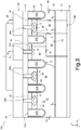
- Figures 3 and 4 show a possible implementation of the power MOS device 10 in Figure 2 .
- Figure 3 is a cross-section of only one portion of the structure in Figure 4 and the entire structure is obtained by flipping Figure 3 about the right-hand edge of same and continuing on both sides.
- the power MOS device 10 is integrated in a die 100 of semiconductor material including a semiconductor body 19 (for example of silicon), having a first conductivity type (for example N) and first and second surfaces 19A, 19B.
- a semiconductor body 19 for example of silicon
- a first conductivity type for example N
- the semiconductor body 19 includes a substrate 21 and an epitaxial layer 23 arranged on top of one another and respectively forming the second and first surfaces 19B, 19A.
- the substrate 21 has a much greater doping level than the epitaxial layer 23 (for example, the substrate 21 has a doping level greater than 10 19 atoms/cm 3 and the epitaxial layer 23 has a doping level comprised between 10 14 and 10 15 atoms/cm 3 ).
- the epitaxial layer 23 includes a drift region 22 having the same conductivity type as the epitaxial layer, but a higher doping level, suited to the breakdown voltage to be sustained (for example greater than 10 16 atoms/cm 3 ).
- the drift region 22 extends between the first surface 19A and the substrate 21 through the entire thickness of the epitaxial layer 23 and, in plan view ( Figure 4 ), is frame-shaped extending close to the periphery of the die 100.
- the epitaxial layer 23 also accommodates a plurality of insulated gate regions 37A-37E (hereinafter referred to as active, inactive and detection gate regions). As shown in Figure 3 , the insulated gate regions 37A-37E extend from the first surface 19A towards the substrate 21 and, in the top view of Figure 4 , parallel to each other and to an axis Y of a Cartesian coordinate system XYZ. Each insulated gate region 37A-37E includes a conductive trench gate region 26, for example of polysilicon, surrounded by an insulating gate layer 27, for example of silicon oxide. The trench gate regions 26 are all electrically coupled together.
- Pairs of adjacent insulated gate regions 37A-37E define respective portions of the epitaxial layer 23 extending parallel to the axis Y.
- the pairs of insulated gate regions 37A-37E delimit two coupling portions 40 (only one shown in Figure 3 ), a plurality of active portions 41 (only one shown in Figure 3 ), two inactive portions 42 (only one shown in Figure 3 ), and two detection portions 43 (only one shown in Figure 3 ).
- the active portions 41 and the inactive portions 42 are formed within the drift region 22.
- Figure 3 shows an active portion 41 arranged between a first and a second active gate regions 37A, 37B and an inactive portion 42 arranged between the second active gate region 37B and an inactive gate region 37C.
- the inactive gate region 42 extends approximately along the longitudinal internal edge (parallel to axis Y) of the drift region 22.
- the coupling portions 40 and the detection portions 43 are arranged in the zone of the epitaxial layer 23 surrounded by the drift region 22.
- Figure 3 shows a coupling portion 40 arranged between the inactive gate region 37C and a first detection gate region 37D, and a detection portion 43 arranged between the first detection gate region 37D and a second detection gate region 37E.
- the active portion 41 accommodates an active channel region 53, of P-type, a first active enriched region 54, of P-type, with a higher doping level than the active channel region 53 (for example with a doping level greater than 5.10 17 atoms/cm 3 ), a second active enriched region 70, of P-type, with a doping level greater than the first active enriched region 54, and an active source region 50 of N-type (for example with a doping level greater than 10 19 atoms/cm 3 ).
- the active source region 50 extends from the first surface 19A
- the active channel region 53 extends beneath the active source region 50
- the first active enriched region 54 extends inside the active channel region 53
- the second active enriched region 70 extends above the first active enriched region 54, at the interface between the active source region 50 and the active channel region 53.
- the detection portion 43 accommodates a detection channel region 57 of P-type, a first enriched detection region 58 of P-type and a greater doping level than the detection channel region 57, a second enriched detection region 73 of P-type and a greater doping level than the first enriched detection region 58, and a detection source region 52 of N-type.
- the detection source region 52 extends from the first surface 19A
- the detection channel region 57 extends beneath the detection source region 52
- the first enriched detection region 58 extends inside the detection channel region 57
- the second enriched detection region 73 extends above the first enriched detection region 58, at the interface between the detection source region 52 and the detection channel region 57.
- the inactive portion 42 accommodates a pseudo-channel region 55 of P-type, a first inactive enriched region of P-type 56 and a higher doping level than the pseudo-channel region 55, and a second inactive enriched region 71 of P-type and a higher doping level than the first inactive enriched region 56.
- the pseudo-channel region 55 extends from the first surface 19A
- the first inactive enriched region 56 extends inside the pseudo-channel region 55
- the second inactive enriched region 71 extends above the first inactive enriched region 56.
- An upper portion of the coupling portion 40 accommodates an enrichment region 51 of N-type and a high doping level (for example equal to the doping level of the active source region 50 and detection source region 52), extending from the first surface 19A. Furthermore, the coupling portion 40 accommodates an enriched coupling region 72 approximately beneath the enrichment region 51.
- the drift region 22 and the regions contained therein form the power MOS transistor 12 of Figure 2
- the detection portion 43 and the regions contained therein form the detection MOS transistor 13 of Figure 2
- the portion of the epitaxial layer beneath the coupling portion 40 and the detection portion 43 define a resistive detection portion 44.
- This forms the detection resistor 14 of Figure 2 represented here by three resistive elements R 1 , R 2 and R 3 , wherein R 1 is connected in series to the parallel circuit formed by R 2 and R 3 .
- the area of the power MOS transistor 12 (approximately corresponding to the area of the drift region 22) is much greater than the area of the detection MOS transistor 13 (which approximately corresponds to the area of the detection portions 43, only one whereof is shown in Figure 3 ) .
- a drain metallization layer 20 (for example comprising three superposed layers of titanium, nickel and gold) extends beneath the second surface 19B and form the drain terminal of the power MOS transistor 12 and of the detection MOS transistor 13, as well as the power supply node 17 in Figure 2 .
- an insulating layer 24 extends above the first surface 19A.
- First and second contact regions 28A, 28B of conductive material extend through the insulating layer 24 as well as in the epitaxial layer 23.
- Each first contact region 28A extends vertically (along a direction Z of the Cartesian coordinate system XYZ) inside a respective portion 41-43 of the epitaxial layer 23, through the channel regions 53, 55, 57 into the second enriched regions 70, 71, 73.
- Each contact region 28B (only one whereof is shown in Figure 3 ) extends vertically (in direction Z) inside a respective portion 40 of the epitaxial layer 23, through the enrichment region 51 into the enriched region 72.
- a source metallization layer 25 of conductive material (such as aluminium) is arranged above the insulating layer 24 and forms (see in particular Figure 4 ) a source metallization region 30 and a detection metallization region 31.
- the source metallization region 30 is trident-shaped, having two outer arms 60, an inner arm 62 and a base 61.
- the outer arms 60 extend parallel to axis Y, substantially above the drift region 22;
- the base 61 extends parallel to axis X above the drift region 22;
- the inner arm 62 extends parallel to axis Y, substantially above the detection portion 43.
- the detection metallization region 31 is U-shaped, substantially complementary to the shape of the source metallization region 30, and has two arms 64 extending above the coupling portions 40 and between the arms 61, 62 of the source metallization region 30.
- the arms 64 of the source metallization region 30 are connected to a pad 65.
- the die 100 also accommodates bias and connection structures of the trench gate region 26 and a pad for the source metallization region 30, not shown.
- the source metallization region 30 is in electrical contact with the contact regions 28A, so as to contact the source regions 53, 57 of the MOS transistors 12, 13.
- the detection metallization region 31 is in electrical contact with the contact regions 28B, so as to contact the coupling portions 40.
- the source metallization region 30 forms the load node 11 of Figure 2 and the detection metallization region 31 forms the detection node 18.
- the first contact regions 28A extend practically for the entire length (in direction Y) of the metallization layer 25, while the second contact regions 28B extend for a length (in direction Y) lower than the length of the coupling and detection portions 40, 43 so as to end at a distance d (for example 6-10 ⁇ m) from the transverse edge parallel to axis X and close to the base 61 of the source metallization region 30 of the drift region 22.
- d for example 6-10 ⁇ m
- the power supply voltage V S is supplied to the drain metallization layer 20 and the drive signal D S is supplied to the gate regions 37A-37E. Furthermore, the pad 65 (corresponding to the node 18 of Figure 2 ) is connected to the detection circuit (not shown) for detecting the potential of the same node.
- the current I 1 supplied by the power MOS transistor 12 flows between the drain metallization layer 20 and the source regions 50, through the drift region 22 and the active channel regions 53.
- the current I 2 supplied by the detection transistor 13 flows between the drain metallization layer 20 and the source regions 52, through the resistive detection portion 44, the detection portions 43 and the detection channel regions 57.
- the voltage drop across the resistive detection portion 44 is detected via the coupling portion 40, the second contact 28B and the detection metallization region 31, enabling detection of the drop on the detection resistor 14 and therefore the current I 2 as well as, using the known surface area ratio, the current I 1 +I 2 supplied to the load.
- the coupling portion 40 dose not contribute to the current I 2 , since the detection node 18 is coupled to an input of the detection circuit (not shown) that is normally high-impedance. Consequently, no current flows through the coupling portion 40 and therefore the resistivity of this coupling portion 40 does not affect the current I 2 .
- Figure 5 shows the plot of the ratio between the areas of the MOS transistors 12, 13 (here defined as K S ) as a function of the variation of the resistance value R S of the detection resistor 14 for the known MOS device 1 of Figure 1 , indicated in Figure 5 with A, and for the power MOS device 10 in Figure 2 , indicated with B, on the basis of simulations carried out by the applicant.
- the curves A and B are obtained by varying the resistance R S of the detection resistor 4 of Figure 1 and of the detection resistor 14 of Figure 2 with respect to a target value defined as the value at which, when the current I 2 flows in the detection resistor 4 and in the detection resistor 14, a voltage drop V KS exists across these resistors, whose value is correlated to the sensitivity of the detection circuit (not shown).
- the voltage drop V KS is compared to a constant threshold value by the detection circuit to generate an intervention signal.
- the parameter K S has a near-constant value.
- the curve A shows that, by varying the resistance R S of the detection resistor 4 by ⁇ 33% with respect to the target value, a variation in the parameter K S of ⁇ 25% is obtained. Consequently, by varying the resistance value R S of the detection resistor 4, and therefore the voltage drop V KS across it, the parameter K S , and therefore the ratio between the areas of the MOS transistors 2, 3, varies considerably and undesirably.
- the curve B (for the power device 10 of Figure 2 ), for the same range of the resistance value of the detection resistor 14, shows a variation in the parameter K S of ⁇ 1.3% in the resistance shown range, and therefore a low variability, as desired.
- Figure 6 shows the behaviour of some electrical quantities as a function of the gate/source voltage V GS of the MOS transistors 12, 13, by biasing the power MOS transistor 12 so as to have a drain/source voltage (V DS ) of 0.1 V, with a gate/source voltage (V GS ) variable between 0 and 5 V.
- V DS drain/source voltage
- V GS gate/source voltage
- the curve C shows the plot of the drain current I D
- the curve D shows plot of the voltage V KS detected on the detection node 18.
- the curves C and D have been measured by the applicant.
- Figures 7-15 show manufacturing steps of the power MOS device 10 shown in Figures 3 and 4 , only for the active area of the device, and therefore omitting the edge areas and the external pads.
- the epitaxial layer 23 is initially grown on the substrate 21, thereby forming the semiconductor body 19.
- the thickness and the doping concentration of the epitaxial layer 23 is such as to ensure the desired breakdown and output impedance performance in the power MOS transistor 12, in a manner known to the person skilled in the art.
- a first protective layer 80 for example of silicon oxide (SiO 2 ) is deposited or thermally grown on the first surface 19A. Then, using known photolithography and ion implantation techniques, shown schematically by arrows 83, an implanted region 82 of N-type is formed, intended to form the drift region 22.
- SiO 2 silicon oxide
- the first protective layer 80 is removed and a plurality of gate trenches 90 is formed from the first surface 19A using known masked wet/dry etching techniques.
- the gate trenches 90 are then filled by thermally growing an insulating gate layer and depositing a filling layer, for example polysilicon of the first conductivity type, doped in situ.
- the portions of the insulating gate layer and of the filling layer on top of the first surface 19A are removed, for example through anisotropic dry etching, soh as to form the trench gate regions 26 and the insulating gate layer 27. thereby, the insulated gate regions 37A-37E are obtained, that delimit the coupling portions 40, the active portions 41, the inactive portions 42 and the detection portions 43.
- a second protective layer 97 of insulating material is deposited on the first surface 19A and a first photoresist mask 91 is formed using known photolithography techniques.
- An ion implantation process indicated in Figure 11 by a plurality of arrows 92, is used to implant P-type ion dopant species, such as boron, thus forming the channel regions 53, 55, 57.
- the first photoresist mask 91 is then removed.
- N-type ionic dopant species such as arsenic
- a second photoresist mask 93 to form the source regions 50, 52 and the enrichment region 51, as shown by arrows 94.
- the second photoresist mask 93 is then removed.
- a high-energy implantation of P-type ionic dopant species such as boron, is performed, as shown by arrows 96.
- the implantation parameters are in particular selected to form the enriched regions 54, 56, 58 at a distance of approximately 600 nm from the first surface 19A, in a known manner. in detail, the enriched regions 54, 58 are formed beneath the source regions 50, 52.
- the third photoresist mask 95 is then removed.
- a dielectric layer 98 for example of silicon oxide, is deposited to form, together with the second protective layer 97, the insulating layer 24 of Figure 3 .
- Contact trenches 102 are then formed in the regions intended to contain the contact regions 28A and 28B.
- the second enriched regions 70-73 are then implanted.
- the contact trenches 102 are then filled with metal material (such as titanium and/or tungsten), thereby forming the plurality of contact regions 28A, 28B.
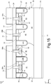
- the source metallization layer 25 is deposited on the upper surface of the insulating layer 24.
- the source metallization region 30 and the detection metallization region 31 are defined using known selective photolithography and etching techniques.
- the drain metallization layer 20 is deposited on the second surface 19B, thus forming the MOS device 10 in Figure 3 .
- Figures 16-17 show a different embodiment of the power MOS device 10. More specifically, Figures 16 and 17 show a power MOS device 210 including a connection MOS transistor 201.
- the power MOS device 210 has a general structure similar to the power MOS device 10 in Figure 2 , so parts similar to those shown and described with reference to Figure 2 are indicated in Figures 16 and 17 using reference signs increased by 200, and are not further described.
- connection MOS transistor 201 is coupled to the detection node 218 and is controlled using the drive signal D S . More specifically, the connection MOS transistor 201 has a gate terminal coupled to the drive node 216, a drain terminal coupled to the detection resistor 214 via the detection node 218 and a source terminal coupled to the external circuitry (not shown) at a detection terminal 202.
- the power MOS device 210 behaves in a manner similar to the manner described for the power MOS device 10 in Figure 2 .
- connection MOS transistor 201 enables the detection resistor 214 to be connected to and disconnected from the external circuitry connected to the detection node 218. In fact, when the power supply voltage V S is low, the connection MOS transistor 201 is off and disconnects the detection resistor 214 from the external circuitry.
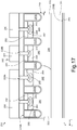
- the power MOS device 210 of Figure 16 may be implemented as shown in Figure 17 .
- the structure of the power MOS device 210 has a structure similar to the power MOS device 10 shown in Figure 2 , except for the fact that the coupling portion 240 accommodates a connection channel region 259 of P-type, in turn accommodating a connection source region 251.
- the connection channel region 259 is similar to the channel regions 254-257 (and to the channel regions 54-57 of Figure 3 ) and may be formed simultaneously with them, by modifying the mask 91 of Figure 11 .
- the connection source region 251 is similar to the enrichment region 51 ( Figure 3 ) and is made in a similar manner ( Figure 12 ).
- Figure 18 shows a different embodiment of the power MOS device, indicated here by 310, including the connection MOS transistor 301.
- the structure of the power MOS device 310 is overall similar to the structure of the power MOS device 210 of Figure 16 and differs only in that the gate terminal of the connection MOS transistor 301 is connected to a dedicated connection terminal 320 receiving a secondary drive signal D S2 .
- the power MOS device 310 is the same as the device of Figure 16 , so similar parts are indicated in Figure 18 using reference signs increased by 100, and are not further described.
- connection MOS transistor 301 has the same function as the connection MOS transistor 201 of Figure 16 , but can be controlled via the drive signal D S2 , regardless of the voltages present in the power MOS device 310. Accordingly, connection of the detection node 318 to the external circuitry for monitoring the current supplied to the load 315 by the power MOS device 310 can be controlled, giving the user greater freedom when monitoring this current.
- the power device described herein has numerous advantages. Indeed, by virtue of the positioning of the detection resistor 14; 214; 314 it is possible to prevent a systematic error and therefore any electrical misalignment between the power MOS transistor 12; 212; 312 and the detection MOS transistor 13; 213; 313, enabling then to operate under the same bias conditions. Furthermore, the inactive portion 42; 242 between the coupling portion 40; 240 and the active portion 41; 241 provides a low-resistance current path and prevents the current to be measured from flowing towards the active portion 41; 241 instead of in the coupling portion 40; 240, and therefore towards the detection node 18; 218. This is also true of the circuit in Figure 18 , having the same implementation shown in Figure 17 .
Landscapes
- Metal-Oxide And Bipolar Metal-Oxide Semiconductor Integrated Circuits (AREA)
Abstract
Description
- This application claims priority from Italian Patent Application No.
102017000046614 filed on April 28, 2017 - The present invention relates to a power MOS device having an integrated current sensor and to the manufacturing process thereof.
- As is known, in power electronic applications, a power MOS device is used to supply a load with a current , which is usually desired to know . Existing power devices therefore often have current detection structures integrated in the power device.
- Many such devices are based on the same MOS technology used for the power device.
- An example of an electric diagram of a known power device integrating a sensor for detecting current is shown in
Figure 1 . - Here, a
power MOS device 1 includes apower MOS transistor 2, the gate terminal of which is coupled to adrive node 6, the drain terminal is coupled to apower supply node 7 and the source terminal is coupled to a first terminal of aload element 5, having a second terminal coupled to a reference-potential line (ground) 9. - Furthermore, the
power MOS device 1 also includes adetection MOS transistor 3, the gate terminal of which is coupled to thedrive node 6, the drain terminal is coupled to thepower supply node 7 and the source terminal is coupled to adetection node 8. - A
detection resistor 4 is arranged between thedetection node 8 and the reference-potential line 9. Alternatively, the detection resistor may be arranged between the source terminals of theMOS transistors - Here, in use, the
power supply node 7 receives a power supply voltage VS. Thedrive node 6 receives a drive signal DS. - The drive signal DS controls the
power MOS transistor 2 and thedetection MOS transistor 3, turning them on via the respective gate terminals. The current flowing through theresistor 4 is monitored by measuring the voltage on thedetection node 8. - Indeed, the current flowing through the
detection resistor 4 and the current flowing through theload element 5 are proportional to one another according to the following equation:
power MOS transistor 2, P3 is the perimeter of the channel of thedetection MOS transistor 3, Ir is the current flowing through thedetection resistor 4 and IL is the current flowing through theload element 5 and supplied by thepower MOS transistor 2. - With the solution of
Figure 1 , by properly dimensioning theMOS transistors detection resistor 4 to be significantly less than the current IL flowing through the load element 5 (for example, 1000 times lower). - The structure shown in
Figure 1 is disadvantageous since there is an electrical misalignment between thepower MOS transistor 2 and thedetection MOS transistor 3 caused by the voltage drop on thedetection resistor 4. - Indeed, the voltage drop on the
detection resistor 4 reduces the gate-source voltage (VGS) of thedetection MOS transistor 3. Consequently, the latter is not subject to the same operating conditions as thepower MOS transistor 2. - This electrical misalignment introduces a systematic error in the measurement of the current supplied to the
load element 5. Furthermore, the error varies depending on the electrical operating region of thepower MOS transistor 2. - In particular, the error is minimal in the saturation region. Conversely, the error is greatest in the linear region and for voltages VGS close to the threshold value. On the other hand, any adjustment for compensating for the error may have unwanted effects on the cost and/or size of the device.
- The aim of the present invention is to provide a power MOS device having an integrated current sensor and a manufacturing process thereof overcoming the drawbacks of the prior art.
- According to the present invention, a power MOS device and the manufacturing process thereof are provided, as defined in the attached claims.
- For a better understanding of the present invention, preferred embodiments thereof will be described only as non-limiting examples, with reference to the attached drawings, wherein:
-
Figure 1 shows the electric diagram of a known power MOS device with an integrated current sensor, -
Figure 2 shows the electric diagram of the present power MOS device, -
Figure 3 shows a cross section of a portion of a possible implementation of the power MOS device ofFigure 2 , -
Figure 4 is a top view of the power MOS device ofFigure 3 , -
Figure 5 shows the behaviour of characteristic quantities of the power MOS device ofFigure 2 , -
Figure 6 shows the behaviour of electrical quantities of the power MOS device ofFigure 2 , -
Figures 7-15 are cross-sections of a silicon die in successive manufacturing steps of the power MOS device ofFigure 3 , -
Figure 16 is an electric diagram of another embodiment of the present power MOS device, -
Figure 17 is a cross-section of the power MOS device inFigure 16 , and -
Figure 18 is a electric diagram of an alternative embodiment of the present power MOS device. -
Figure 2 shows apower MOS device 10 comprising apower MOS transistor 12 and adetection MOS transistor 13. - The
power MOS transistor 12 has a gate terminal coupled to adrive node 16, a drain terminal coupled to apower supply node 17 and a source terminal forming aload node 11.Figure 2 also shows a load 15 (typically outside the power MOS device 10) intended to be coupled between theload node 11 and a reference-potential line (ground). - The
detection MOS transistor 13 has a gate terminal coupled to thedrive node 16, a drain terminal forming adetection node 18 and a source terminal coupled to theload node 11. - A
detection resistor 14 has a first terminal coupled to thepower supply node 17 and a second terminal coupled to thedetection node 18. - In use, the
power supply node 17 receives a power supply voltage VS and thedrive node 16 receives a drive signal DS, in a known manner. - Furthermore, the
detection MOS transistor 13 and thedetection resistor 14 detect the current supplied by thepower MOS transistor 12 to theload 15. - In fact, the
power MOS transistor 12 and thedetection MOS transistor 13 have the same voltage drop VGS between the gate and source terminals, and are therefore under the same biasing conditions. Therefore, they conduct respective currents I1, I2 proportional to one another according to the equation (1). - The current I2 flowing in the
detection MOS transistor 13 also flows in thedetection resistor 14 and may be determined from the voltage drop on thedetection resistor 14, by detecting the potential on thedetection node 18. - The
power MOS device 10 addresses the problem of electrical misalignment between thepower MOS transistor 12 and thedetection MOS transistor 13, since they are biased in exactly the same manner, as previously specified. Thepower MOS device 10 is therefore not affected by the electrical misalignment and systematic error of the known power device inFigure 1 . - In the
power MOS device 10, both currents I1 (flowing in the power MOS transistor 12) and I2 (flowing in the detection MOS transistor 13) are supplied to theload 15. Consequently, the power MOS device 10has a high efficiency and enables a very wide choice of the area ratio between theMOS transistors -
Figures 3 and4 show a possible implementation of thepower MOS device 10 inFigure 2 . In particular,Figure 3 is a cross-section of only one portion of the structure inFigure 4 and the entire structure is obtained by flippingFigure 3 about the right-hand edge of same and continuing on both sides. - The
power MOS device 10 is integrated in adie 100 of semiconductor material including a semiconductor body 19 (for example of silicon), having a first conductivity type (for example N) and first andsecond surfaces - The
semiconductor body 19 includes asubstrate 21 and anepitaxial layer 23 arranged on top of one another and respectively forming the second andfirst surfaces substrate 21 has a much greater doping level than the epitaxial layer 23 (for example, thesubstrate 21 has a doping level greater than 1019 atoms/cm3 and theepitaxial layer 23 has a doping level comprised between 1014 and 1015 atoms/cm3). - The
epitaxial layer 23 includes adrift region 22 having the same conductivity type as the epitaxial layer, but a higher doping level, suited to the breakdown voltage to be sustained (for example greater than 1016 atoms/cm3). Thedrift region 22 extends between thefirst surface 19A and thesubstrate 21 through the entire thickness of theepitaxial layer 23 and, in plan view (Figure 4 ), is frame-shaped extending close to the periphery of thedie 100. - The
epitaxial layer 23 also accommodates a plurality of insulatedgate regions 37A-37E (hereinafter referred to as active, inactive and detection gate regions). As shown inFigure 3 , theinsulated gate regions 37A-37E extend from thefirst surface 19A towards thesubstrate 21 and, in the top view ofFigure 4 , parallel to each other and to an axis Y of a Cartesian coordinate system XYZ. Each insulatedgate region 37A-37E includes a conductivetrench gate region 26, for example of polysilicon, surrounded by aninsulating gate layer 27, for example of silicon oxide. Thetrench gate regions 26 are all electrically coupled together. - Pairs of adjacent
insulated gate regions 37A-37E define respective portions of theepitaxial layer 23 extending parallel to the axis Y. In particular, in the present embodiment, the pairs ofinsulated gate regions 37A-37E delimit two coupling portions 40 (only one shown inFigure 3 ), a plurality of active portions 41 (only one shown inFigure 3 ), two inactive portions 42 (only one shown inFigure 3 ), and two detection portions 43 (only one shown inFigure 3 ). - The
active portions 41 and theinactive portions 42 are formed within thedrift region 22. In particular,Figure 3 shows anactive portion 41 arranged between a first and a secondactive gate regions inactive portion 42 arranged between the secondactive gate region 37B and aninactive gate region 37C. As shown inFigure 3 , theinactive gate region 42 extends approximately along the longitudinal internal edge (parallel to axis Y) of thedrift region 22. - The
coupling portions 40 and thedetection portions 43 are arranged in the zone of theepitaxial layer 23 surrounded by thedrift region 22. In particular,Figure 3 shows acoupling portion 40 arranged between theinactive gate region 37C and a firstdetection gate region 37D, and adetection portion 43 arranged between the firstdetection gate region 37D and a seconddetection gate region 37E. - The
active portion 41 accommodates anactive channel region 53, of P-type, a first active enrichedregion 54, of P-type, with a higher doping level than the active channel region 53 (for example with a doping level greater than 5.1017 atoms/cm3), a second active enrichedregion 70, of P-type, with a doping level greater than the first active enrichedregion 54, and anactive source region 50 of N-type (for example with a doping level greater than 1019 atoms/cm3). In detail, theactive source region 50 extends from thefirst surface 19A, theactive channel region 53 extends beneath theactive source region 50, the first active enrichedregion 54 extends inside theactive channel region 53, and the second active enrichedregion 70 extends above the first active enrichedregion 54, at the interface between theactive source region 50 and theactive channel region 53. - Similarly, the
detection portion 43 accommodates adetection channel region 57 of P-type, a first enricheddetection region 58 of P-type and a greater doping level than thedetection channel region 57, a second enricheddetection region 73 of P-type and a greater doping level than the first enricheddetection region 58, and adetection source region 52 of N-type. Thedetection source region 52 extends from thefirst surface 19A, thedetection channel region 57 extends beneath thedetection source region 52, the first enricheddetection region 58 extends inside thedetection channel region 57, and the second enricheddetection region 73 extends above the first enricheddetection region 58, at the interface between thedetection source region 52 and thedetection channel region 57. - The
inactive portion 42 accommodates apseudo-channel region 55 of P-type, a first inactive enriched region of P-type 56 and a higher doping level than thepseudo-channel region 55, and a second inactive enrichedregion 71 of P-type and a higher doping level than the first inactive enrichedregion 56. Thepseudo-channel region 55 extends from thefirst surface 19A, the first inactive enrichedregion 56 extends inside thepseudo-channel region 55, and the second inactive enrichedregion 71 extends above the first inactive enrichedregion 56. - An upper portion of the
coupling portion 40 accommodates anenrichment region 51 of N-type and a high doping level (for example equal to the doping level of theactive source region 50 and detection source region 52), extending from thefirst surface 19A. Furthermore, thecoupling portion 40 accommodates an enrichedcoupling region 72 approximately beneath theenrichment region 51. - In practice, the
drift region 22 and the regions contained therein form thepower MOS transistor 12 ofFigure 2 , thedetection portion 43 and the regions contained therein form thedetection MOS transistor 13 ofFigure 2 . As explained in greater detail below, the portion of the epitaxial layer beneath thecoupling portion 40 and thedetection portion 43 define aresistive detection portion 44. This forms thedetection resistor 14 ofFigure 2 , represented here by three resistive elements R1, R2 and R3, wherein R1 is connected in series to the parallel circuit formed by R2 and R3. - Furthermore, as shown in the top view of
Figure 4 , the area of the power MOS transistor 12 (approximately corresponding to the area of the drift region 22) is much greater than the area of the detection MOS transistor 13 (which approximately corresponds to the area of thedetection portions 43, only one whereof is shown inFigure 3 ) . - A drain metallization layer 20 (for example comprising three superposed layers of titanium, nickel and gold) extends beneath the
second surface 19B and form the drain terminal of thepower MOS transistor 12 and of thedetection MOS transistor 13, as well as thepower supply node 17 inFigure 2 . - Furthermore, an insulating
layer 24, for example of silicon oxide (SiO2) extends above thefirst surface 19A. First andsecond contact regions layer 24 as well as in theepitaxial layer 23. Eachfirst contact region 28A extends vertically (along a direction Z of the Cartesian coordinate system XYZ) inside a respective portion 41-43 of theepitaxial layer 23, through thechannel regions regions contact region 28B (only one whereof is shown inFigure 3 ) extends vertically (in direction Z) inside arespective portion 40 of theepitaxial layer 23, through theenrichment region 51 into the enrichedregion 72. - A
source metallization layer 25 of conductive material (such as aluminium) is arranged above the insulatinglayer 24 and forms (see in particularFigure 4 ) asource metallization region 30 and adetection metallization region 31. As shown in particular inFigure 4 , thesource metallization region 30 is trident-shaped, having twoouter arms 60, aninner arm 62 and abase 61. Theouter arms 60 extend parallel to axis Y, substantially above thedrift region 22; thebase 61 extends parallel to axis X above thedrift region 22; and theinner arm 62 extends parallel to axis Y, substantially above thedetection portion 43. Thedetection metallization region 31 is U-shaped, substantially complementary to the shape of thesource metallization region 30, and has twoarms 64 extending above thecoupling portions 40 and between thearms source metallization region 30. Thearms 64 of thesource metallization region 30 are connected to apad 65. Thedie 100 also accommodates bias and connection structures of thetrench gate region 26 and a pad for thesource metallization region 30, not shown. - The
source metallization region 30 is in electrical contact with thecontact regions 28A, so as to contact thesource regions MOS transistors detection metallization region 31 is in electrical contact with thecontact regions 28B, so as to contact thecoupling portions 40. In practice, thesource metallization region 30 forms theload node 11 ofFigure 2 and thedetection metallization region 31 forms thedetection node 18. - As shown in
Figure 4 , thefirst contact regions 28A extend practically for the entire length (in direction Y) of themetallization layer 25, while thesecond contact regions 28B extend for a length (in direction Y) lower than the length of the coupling anddetection portions base 61 of thesource metallization region 30 of thedrift region 22. - In use, the power supply voltage VS is supplied to the
drain metallization layer 20 and the drive signal DS is supplied to thegate regions 37A-37E. Furthermore, the pad 65 (corresponding to thenode 18 ofFigure 2 ) is connected to the detection circuit (not shown) for detecting the potential of the same node. The current I1 supplied by thepower MOS transistor 12 flows between thedrain metallization layer 20 and thesource regions 50, through thedrift region 22 and theactive channel regions 53. - The presence of the
inactive portion 42 on the edge of thedrift region 22 between theactive portion 41 and thecoupling portion 40, as well as the distance d between the transverse edge (parallel to axis X inFigure 4 ) of thedrift region 22 and the end of thesecond contact regions 28B prevent the current I1 from flowing towards thecoupling region 40, causing a voltage drop on this latter and a detection error. - The current I2 supplied by the
detection transistor 13 flows between thedrain metallization layer 20 and thesource regions 52, through theresistive detection portion 44, thedetection portions 43 and thedetection channel regions 57. - The voltage drop across the
resistive detection portion 44 is detected via thecoupling portion 40, thesecond contact 28B and thedetection metallization region 31, enabling detection of the drop on thedetection resistor 14 and therefore the current I2 as well as, using the known surface area ratio, the current I1+I2 supplied to the load. - It can be seen that the
coupling portion 40 dose not contribute to the current I2, since thedetection node 18 is coupled to an input of the detection circuit (not shown) that is normally high-impedance. Consequently, no current flows through thecoupling portion 40 and therefore the resistivity of thiscoupling portion 40 does not affect the current I2. -
Figure 5 shows the plot of the ratio between the areas of theMOS transistors 12, 13 (here defined as KS) as a function of the variation of the resistance value RS of thedetection resistor 14 for the knownMOS device 1 ofFigure 1 , indicated inFigure 5 with A, and for thepower MOS device 10 inFigure 2 , indicated with B, on the basis of simulations carried out by the applicant. In particular, the curves A and B are obtained by varying the resistance RS of thedetection resistor 4 ofFigure 1 and of thedetection resistor 14 ofFigure 2 with respect to a target value defined as the value at which, when the current I2 flows in thedetection resistor 4 and in thedetection resistor 14, a voltage drop VKS exists across these resistors, whose value is correlated to the sensitivity of the detection circuit (not shown). The voltage drop VKS is compared to a constant threshold value by the detection circuit to generate an intervention signal. In general, the parameter KS has a near-constant value. - In particular, the curve A (for the known
device 1 ofFigure 1 ) shows that, by varying the resistance RS of thedetection resistor 4 by ±33% with respect to the target value, a variation in the parameter KS of ±25% is obtained. Consequently, by varying the resistance value RS of thedetection resistor 4, and therefore the voltage drop VKS across it, the parameter KS, and therefore the ratio between the areas of theMOS transistors - Conversely, the curve B (for the
power device 10 ofFigure 2 ), for the same range of the resistance value of thedetection resistor 14, shows a variation in the parameter KS of ± 1.3% in the resistance shown range, and therefore a low variability, as desired. - In practice therefore, the designer has greater freedom to select the resistance value RS of the
detection resistor 14, regardless of the desired area ratio for theMOS transistors -
Figure 6 shows the behaviour of some electrical quantities as a function of the gate/source voltage VGS of theMOS transistors power MOS transistor 12 so as to have a drain/source voltage (VDS) of 0.1 V, with a gate/source voltage (VGS) variable between 0 and 5 V. In particular, the curve C shows the plot of the drain current ID, and the curve D shows plot of the voltage VKS detected on thedetection node 18. The curves C and D have been measured by the applicant. - More specifically, after the
power MOS transistor 12 has been turned on, VGS ≈ 2 V, the drain current ID increases and the voltage on thedetection node 18 drops correspondingly, confirming the correct detection of the current in thepower MOS transistor 12. -
Figures 7-15 show manufacturing steps of thepower MOS device 10 shown inFigures 3 and4 , only for the active area of the device, and therefore omitting the edge areas and the external pads. - With reference to
Figure 7 , theepitaxial layer 23 is initially grown on thesubstrate 21, thereby forming thesemiconductor body 19. The thickness and the doping concentration of theepitaxial layer 23 is such as to ensure the desired breakdown and output impedance performance in thepower MOS transistor 12, in a manner known to the person skilled in the art. - Subsequently,
Figure 8 , a firstprotective layer 80, for example of silicon oxide (SiO2) is deposited or thermally grown on thefirst surface 19A. Then, using known photolithography and ion implantation techniques, shown schematically byarrows 83, an implantedregion 82 of N-type is formed, intended to form thedrift region 22. - Thereafter,
Figure 9 , a heat treatment is performed to diffuse the ions of the implantedregion 82, thereby obtaining thedrift region 22. - Subsequently,
Figure 10 , the firstprotective layer 80 is removed and a plurality ofgate trenches 90 is formed from thefirst surface 19A using known masked wet/dry etching techniques. Thegate trenches 90 are then filled by thermally growing an insulating gate layer and depositing a filling layer, for example polysilicon of the first conductivity type, doped in situ. The portions of the insulating gate layer and of the filling layer on top of thefirst surface 19A are removed, for example through anisotropic dry etching, soh as to form thetrench gate regions 26 and the insulatinggate layer 27. thereby, theinsulated gate regions 37A-37E are obtained, that delimit thecoupling portions 40, theactive portions 41, theinactive portions 42 and thedetection portions 43. - Then,
Figure 11 , a secondprotective layer 97 of insulating material is deposited on thefirst surface 19A and afirst photoresist mask 91 is formed using known photolithography techniques. An ion implantation process, indicated inFigure 11 by a plurality ofarrows 92, is used to implant P-type ion dopant species, such as boron, thus forming thechannel regions first photoresist mask 91 is then removed. - Then,
Figure 12 , N-type ionic dopant species, such as arsenic, are implanted using asecond photoresist mask 93 to form thesource regions enrichment region 51, as shown byarrows 94. Thesecond photoresist mask 93 is then removed. - Using a
third photoresist mask 95,Figure 13 , a high-energy implantation of P-type ionic dopant species, such as boron, is performed, as shown byarrows 96. The implantation parameters are in particular selected to form the enrichedregions first surface 19A, in a known manner. in detail, the enrichedregions source regions third photoresist mask 95 is then removed. - Subsequently,
Figure 14 , adielectric layer 98, for example of silicon oxide, is deposited to form, together with the secondprotective layer 97, the insulatinglayer 24 ofFigure 3 . Contacttrenches 102 are then formed in the regions intended to contain thecontact regions contact trenches 102 are then filled with metal material (such as titanium and/or tungsten), thereby forming the plurality ofcontact regions - Finally,
Figure 15 , thesource metallization layer 25 is deposited on the upper surface of the insulatinglayer 24. Thesource metallization region 30 and thedetection metallization region 31 are defined using known selective photolithography and etching techniques. Furthermore, thedrain metallization layer 20 is deposited on thesecond surface 19B, thus forming theMOS device 10 inFigure 3 . -
Figures 16-17 show a different embodiment of thepower MOS device 10. More specifically,Figures 16 and17 show apower MOS device 210 including aconnection MOS transistor 201. Thepower MOS device 210 has a general structure similar to thepower MOS device 10 inFigure 2 , so parts similar to those shown and described with reference toFigure 2 are indicated inFigures 16 and17 using reference signs increased by 200, and are not further described. - The
connection MOS transistor 201 is coupled to thedetection node 218 and is controlled using the drive signal DS. More specifically, theconnection MOS transistor 201 has a gate terminal coupled to thedrive node 216, a drain terminal coupled to thedetection resistor 214 via thedetection node 218 and a source terminal coupled to the external circuitry (not shown) at adetection terminal 202. - In use, the
power MOS device 210 behaves in a manner similar to the manner described for thepower MOS device 10 inFigure 2 . - More specifically, the
connection MOS transistor 201 enables thedetection resistor 214 to be connected to and disconnected from the external circuitry connected to thedetection node 218. In fact, when the power supply voltage VS is low, theconnection MOS transistor 201 is off and disconnects thedetection resistor 214 from the external circuitry. - The
power MOS device 210 ofFigure 16 may be implemented as shown inFigure 17 . - As visible, the structure of the
power MOS device 210 has a structure similar to thepower MOS device 10 shown inFigure 2 , except for the fact that thecoupling portion 240 accommodates aconnection channel region 259 of P-type, in turn accommodating aconnection source region 251. Theconnection channel region 259 is similar to the channel regions 254-257 (and to the channel regions 54-57 ofFigure 3 ) and may be formed simultaneously with them, by modifying themask 91 ofFigure 11 . Theconnection source region 251 is similar to the enrichment region 51 (Figure 3 ) and is made in a similar manner (Figure 12 ). -
Figure 18 shows a different embodiment of the power MOS device, indicated here by 310, including theconnection MOS transistor 301. The structure of thepower MOS device 310 is overall similar to the structure of thepower MOS device 210 ofFigure 16 and differs only in that the gate terminal of theconnection MOS transistor 301 is connected to adedicated connection terminal 320 receiving a secondary drive signal DS2. In all other aspects, thepower MOS device 310 is the same as the device ofFigure 16 , so similar parts are indicated inFigure 18 using reference signs increased by 100, and are not further described. - In use, the
connection MOS transistor 301 has the same function as theconnection MOS transistor 201 ofFigure 16 , but can be controlled via the drive signal DS2, regardless of the voltages present in thepower MOS device 310. Accordingly, connection of thedetection node 318 to the external circuitry for monitoring the current supplied to theload 315 by thepower MOS device 310 can be controlled, giving the user greater freedom when monitoring this current. - The power device described herein has numerous advantages. Indeed, by virtue of the positioning of the
detection resistor 14; 214; 314 it is possible to prevent a systematic error and therefore any electrical misalignment between thepower MOS transistor 12; 212; 312 and thedetection MOS transistor 13; 213; 313, enabling then to operate under the same bias conditions. Furthermore, theinactive portion 42; 242 between thecoupling portion 40; 240 and theactive portion 41; 241 provides a low-resistance current path and prevents the current to be measured from flowing towards theactive portion 41; 241 instead of in thecoupling portion 40; 240, and therefore towards thedetection node 18; 218. This is also true of the circuit inFigure 18 , having the same implementation shown inFigure 17 . - It is evident that modifications and variations may be made to the device and method described and illustrated without thereby departing from the scope of the present invention, as defined in the attached claims. For example, the conductivity types may be inverted.
Claims (15)
- A power MOS device (10; 210; 310) comprising:a power MOS transistor (12; 212; 312) having a first conduction terminal, a gate terminal and a second conduction terminal, the first conduction terminal of the power MOS transistor (12; 212; 312) being coupled to a reference-potential node (17; 217; 317), the gate terminal of the power MOS transistor (12; 212; 312) being coupled to a drive node (16; 216; 316) and the second conduction terminal of the power MOS transistor (12; 212; 312) being coupled to a load node (11; 211; 311),a detection MOS transistor (13; 213; 313) having a first conduction terminal, a gate terminal and a second conduction terminal, the first conduction terminal of the detection MOS transistor (13; 213; 313) being coupled to a detection node (18; 218; 318), the gate terminal of the detection MOS transistor (13; 213; 313) being coupled to the drive node (16; 216; 316) and the second conduction terminal of the detection MOS transistor (13; 213; 313) being coupled to the load node (11; 211; 311),a detection resistor (14; 214; 314) having first and second terminals, the first terminal being coupled to the reference-potential node (17; 217; 317) and the second terminal being coupled to the detection node (18; 218; 318).
- The device according to claim 1, further comprising a switch (201; 301) electrically coupled to the second terminal of the detection resistor and configured to selectively electrically couple the detection resistor to the detection node (218; 318).
- The device according to claim 2, wherein the switch includes a connection MOS transistor (201; 301) having a first conduction terminal, a control terminal and a second conduction terminal, the first conduction terminal of the connection MOS transistor (201; 301) being coupled to the detection node (218; 318), the control terminal of the connection MOS transistor (201; 301) being configured to receive a drive signal (DS, DS2) and the second conduction terminal of the connection MOS transistor (201; 301) forming a detection terminal (202; 302).
- The device according to claim 3, wherein the control terminal of the connection MOS transistor (201; 301) is coupled to the drive node (216).
- The device according to any one of claims 1-4, comprising:a semiconductor body (19; 219) having a first conductivity type, a first surface (19A; 219A) and a second surface (19B; 219B),a plurality of insulated gate regions (37A-37E; 237A-237E) extending inside the semiconductor body (19; 219) from the first surface (19A; 219A),a first channel region (53; 253) of a second conductivity type, extending between a first insulated gate region (37A; 237A) and a second insulated gate region (37B; 237B), adjacent to each other, of the plurality of insulated gate regions (37A-37E; 237A-237E),a second channel region (57; 257) of the second conductivity type, extending inside the body between a third insulated gate region (37D; 237D) and a fourth insulated gate region (37E; 237E), adjacent to each other, of the plurality of insulated gate regions (37A-37E; 237A-237E),a first source region (50; 250) of the first conductivity type, extending between the first channel region (53; 253) and the first surface (19A; 219A) of the semiconductor body (19; 219), the first source region (50; 250), the first channel region (53; 253), the first insulated gate region (37A; 237A) and the second insulated gate region (37B; 237B) forming the power MOS transistor (12; 212; 312),a second source region (52; 252), of the first conductivity type, extending between the second channel region (57; 257) and the first surface (19A; 219A) of the semiconductor body (19; 219), the second source region (52; 252), the second channel region (57; 257), the third insulated gate region (37D; 237D) and the fourth insulated gate region (37E; 237E) forming the detection MOS transistor (13; 213; 313);a portion of the semiconductor body (19; 219) extending beneath the first surface (19A; 219A) of the semiconductor body (19; 219), between the third insulated gate region (37D; 237D) and a fifth insulated gate region (37C; 237C) of the plurality of insulated gate regions (37A-37E; 237A-237E) forming a coupling portion (40; 240),a first contact region (28B; 228B) extending from the first surface (19A; 219A) into the coupling portion (40; 240) and forming the detection node (18; 218; 318),a resistive detection portion (44; 244) of the semiconductor body (19; 219) arranged beneath the coupling portion (40; 240) and forming the detection resistor (14; 214; 314).
- The device according to claim 5, further comprising an enrichment region (51; 251) having the first conductivity type and a higher doping level than the body (19; 219), the enrichment region (51; 251) extending between the coupling portion (40; 240) and the first surface (19A; 219A) of the semiconductor body (19; 219) .
- The device according to claim 6 when dependent on claims 3 or 4 and 5, further comprising a connection channel region (259) having the second conductivity type, the connection channel region (259) extending inside the semiconductor body (219) beneath the enrichment region (251), and forming the connection MOS transistor (201; 301), together with the enrichment region (251), the coupling portion (240), the third insulated gate region (237D) and the fifth insulated gate region (237C).
- The device according to any of claims 5-7, further comprising a drift region (22; 222) having the first conductivity type and a higher doping level than the body (19; 219), the drift region (22; 222) extending between the first surface (19A; 219A) and the second surface (19B; 219B), accommodating the first insulated gate region (37A; 237A) and the second insulated gate region (37B; 237B), and being laterally delimited in part by the first insulated gate region (37C; 237C), the portion of the drift region (22; 222) arranged between the second gate region (37B; 237B) and the fifth gate region (37C; 237C) forming an inactive portion (42; 242).
- The device according to any of claims 5-8, further comprising a second contact region (28A; 228A) and a third contact region (28A; 228A) extending from the first surface (19A; 219A) into the body (19; 219), the second contact region (28A; 228A) extending through the first source region (50; 250) and the first channel region (53; 253), the third contact region (28A; 228A) extending through the second source region (52; 252) and the second channel region (57; 257), the second contact region (28A; 228A) and the third contact region (28A; 228A) being in electrical contact with a source metallization region (30; 230) extending above the first surface (19A; 219A), the first contact region (28B; 228B) being in electrical contact with a detection metallization region (31; 231); the source metallization region (30; 230)and the detection metallization region (31; 231) being formed on a same metallization level (25; 225).
- A process for manufacturing a device (10; 210; 310) comprising forming, in a semiconductor body (19; 219) having a first surface (19A; 219A) and a second surface (19B; 219B):a power MOS transistor (12; 212; 312) having a first conduction region, a gate region and a second conduction region, the first conduction region of the power MOS transistor (12; 212; 312) being coupled to a reference potential node (17; 217; 317), the second conduction region of the power MOS transistor (12; 212; 312) being coupled to a load node (11; 211; 311) and the gate region of the power MOS transistor (12; 212; 312) being coupled to a drive node (16; 216; 316),a detection MOS transistor (13; 213; 313) having a first conduction region, a gate region and a second conduction region, the first conduction region of the detection MOS transistor (13; 213; 313) being coupled to a detection node (18; 218; 318), the second conduction region of the detection MOS transistor (13; 213; 313) being coupled to the load node (11; 211; 311) and the gate region of the detection MOS transistor (13; 213; 313) being coupled to the drive node (16; 216; 316), anda detection resistor (14; 214; 314) having a first terminal coupled to the reference-potential node (17; 217; 317) and a second terminal coupled to the detection node (18; 218; 318),the process further comprising:forming a first metallization region (30; 230) on the first surface (19A; 219A) and in electrical contact with the second conduction region of the power MOS transistor (12; 212; 312) and the second conduction region of the detection MOS transistor (13; 213; 313),forming a detection metallization region (31; 231) on the first surface (19A; 219A) coupled to the detection node (18; 218; 318), andforming a second metallization region (20; 220) on the second surface (19B; 219B) and in electrical contact with the first conduction region of the power MOS transistor (12; 212; 312) and coupled to the reference-potential node (17; 217; 317).
- A process according to claim 10, wherein the semiconductor body (19; 219) has a first conductivity type and forming a power MOS transistor (12; 212; 312) and a detection MOS transistor (13; 213; 313) comprise:forming a plurality of insulated gate regions (37A-37E; 237A-237E) inside the semiconductor body (19; 219) from the first surface (19A; 219A), the plurality of insulated gate regions (37A-37E; 237A-237E) including a first insulated gate region (37A; 237A), a second insulated gate region (37B; 237B), a third insulated gate region (37D; 237D), a fourth insulated gate region (37E; 237E) and a fifth insulated gate region (37C; 237C), a portion of the semiconductor body (19; 219) between the third insulated gate region (37D; 237D) and the fifth insulated gate region (37C; 237C) forming a coupling portion (40; 240),introducing ionic dopant species of a second conductivity type into a first portion (41; 241) of the semiconductor body (19; 219) arranged between the first insulated gate region (37A; 237A) and the second insulated gate region (37B; 237B) and into a second portion (43; 243) of the body arranged between the third insulated gate region (37D; 237D) and the fourth insulated gate region (37E; 237E) to form a first channel region (53; 253) and a second channel region (57; 257),introducing ionic dopant species of the first conductivity type into the first channel region (53; 253) and the second channel region (57; 257) to form the second conduction region (50; 250) of the power MOS transistor (12; 212; 312) and the second conduction region (52; 252) of the detection MOS transistor (13; 213; 313), andforming contact regions (28A, 28B; 228A, 228B) inside the first portion (41; 241), the second portion (43; 243) and the coupling portion (40; 240), the contact regions (28A, 28B; 228A, 228B) extending from the first surface (19A; 219A) towards the second surface (19B; 219B).
- A process according to claim 11, further comprising introducing ionic dopant species of the first conductivity type into the coupling portion (40; 240), forming an enrichment region (51; 251) adjacent to the first surface (19A; 219A).
- A process according to claim 12, further comprising introducing ionic dopant species of the second conductivity type into the coupling portion (240), forming a connection channel region (259) extending inside the semiconductor body (219) beneath the enrichment region (251).
- A process according to any of claims 11-13, further comprising, before forming a plurality of insulated gate regions (37A-37E; 237A-237E), diffusing ionic dopant species of the first conductivity type into the semiconductor body (19; 219), in an area intended to contain the first insulated gate region (37A; 237A) and the second insulated gate region (37B; 237B), forming a drift region (22; 222) extending between the first surface (19A; 219A) and the second surface (19B; 219B) and intended to be laterally delimited in part by the fifth gate region (37C; 237C).
- A process according to any one of claims 10-14, further comprising forming a metallization layer (25; 225) above the first surface (19A; 219A) and shaping the metallization layer (25; 225) to form the detection metallization region (31; 231) and the first metallization region (30; 230).
Applications Claiming Priority (1)
| Application Number | Priority Date | Filing Date | Title |
|---|---|---|---|
| IT102017000046614A IT201700046614A1 (en) | 2017-04-28 | 2017-04-28 | MOS POWER DEVICE WITH INTEGRATED CURRENT SENSOR AND ITS MANUFACTURING PROCESS |
Publications (2)
| Publication Number | Publication Date |
|---|---|
| EP3396718A1 true EP3396718A1 (en) | 2018-10-31 |
| EP3396718B1 EP3396718B1 (en) | 2021-10-06 |
Family
ID=59811882
Family Applications (1)
| Application Number | Title | Priority Date | Filing Date |
|---|---|---|---|
| EP18168154.5A Active EP3396718B1 (en) | 2017-04-28 | 2018-04-19 | Power mos device having an integrated current sensor and manufacturing process thereof |
Country Status (4)
| Country | Link |
|---|---|
| US (2) | US10943896B2 (en) |
| EP (1) | EP3396718B1 (en) |
| CN (3) | CN116364714A (en) |
| IT (1) | IT201700046614A1 (en) |
Cited By (1)
| Publication number | Priority date | Publication date | Assignee | Title |
|---|---|---|---|---|
| IT202000001942A1 (en) | 2020-01-31 | 2021-07-31 | St Microelectronics Srl | ELECTRONIC POWER DEVICE WITH VERTICAL CONDUCTION WITH REDUCED IGNITION RESISTANCE AND RELATED MANUFACTURING PROCESS |
Families Citing this family (4)
| Publication number | Priority date | Publication date | Assignee | Title |
|---|---|---|---|---|
| IT201700046614A1 (en) * | 2017-04-28 | 2018-10-28 | St Microelectronics Srl | MOS POWER DEVICE WITH INTEGRATED CURRENT SENSOR AND ITS MANUFACTURING PROCESS |
| IT201800007780A1 (en) | 2018-08-02 | 2020-02-02 | St Microelectronics Srl | SILICON CARBIDE MOSFET DEVICE AND ITS MANUFACTURING METHOD |
| CN112289787B (en) * | 2020-09-17 | 2024-01-26 | 南京通华芯微电子有限公司 | A MOS device with multiple control functions |
| TWI867430B (en) * | 2023-02-13 | 2024-12-21 | 通嘉科技股份有限公司 | High-voltage tolerant device and detection circuit |
Citations (7)
| Publication number | Priority date | Publication date | Assignee | Title |
|---|---|---|---|---|
| US4931844A (en) * | 1988-03-09 | 1990-06-05 | Ixys Corporation | High power transistor with voltage, current, power, resistance, and temperature sensing capability |
| JPH05167077A (en) * | 1991-12-12 | 1993-07-02 | Nec Kansai Ltd | Semiconductor device |
| US5408141A (en) * | 1993-01-04 | 1995-04-18 | Texas Instruments Incorporated | Sensed current driving device |
| JPH10326897A (en) * | 1997-03-25 | 1998-12-08 | Hitachi Ltd | Trench gate semiconductor device with current detection cell |
| US7932553B2 (en) * | 2007-12-24 | 2011-04-26 | Denso Corporation | Semiconductor device including a plurality of cells |
| JP2012060069A (en) * | 2010-09-13 | 2012-03-22 | Denso Corp | Semiconductor device |
| US20130001792A1 (en) * | 2011-06-30 | 2013-01-03 | Renesas Electronics Corporation | Semiconductor device |
Family Cites Families (11)
| Publication number | Priority date | Publication date | Assignee | Title |
|---|---|---|---|---|
| EP1450411A1 (en) * | 2003-02-21 | 2004-08-25 | STMicroelectronics S.r.l. | MOS power device with high integration density and manufacturing process thereof |
| CN103022115B (en) * | 2008-01-29 | 2015-09-02 | 富士电机株式会社 | Semiconductor device |
| DE112009004805B4 (en) * | 2009-05-28 | 2019-03-28 | Toyota Jidosha Kabushiki Kaisha | SEMICONDUCTOR DEVICE |
| JP5553652B2 (en) * | 2010-03-18 | 2014-07-16 | ルネサスエレクトロニクス株式会社 | Semiconductor substrate and semiconductor device |
| US9349854B2 (en) * | 2013-10-04 | 2016-05-24 | Infineon Technologies Ag | Semiconductor device and method of manufacturing the same |
| DE102014106825B4 (en) * | 2014-05-14 | 2019-06-27 | Infineon Technologies Ag | Semiconductor device |
| DE102014113254B4 (en) * | 2014-09-15 | 2017-07-13 | Infineon Technologies Austria Ag | Semiconductor device with current sensor |
| DE102014114230B4 (en) * | 2014-09-30 | 2021-10-07 | Infineon Technologies Ag | Semiconductor device and manufacturing method therefor |
| DE102014226161B4 (en) * | 2014-12-17 | 2017-10-26 | Infineon Technologies Ag | Semiconductor device with overload current capability |
| CN106601710B (en) * | 2015-10-19 | 2021-01-29 | 富士电机株式会社 | Semiconductor device and method for manufacturing semiconductor device |
| IT201700046614A1 (en) * | 2017-04-28 | 2018-10-28 | St Microelectronics Srl | MOS POWER DEVICE WITH INTEGRATED CURRENT SENSOR AND ITS MANUFACTURING PROCESS |
-
2017
- 2017-04-28 IT IT102017000046614A patent/IT201700046614A1/en unknown
-
2018
- 2018-04-12 CN CN202310285620.3A patent/CN116364714A/en active Pending
- 2018-04-12 CN CN201820518315.9U patent/CN208722876U/en active Active
- 2018-04-12 CN CN201810326240.9A patent/CN108807366B/en active Active
- 2018-04-19 EP EP18168154.5A patent/EP3396718B1/en active Active
- 2018-04-27 US US15/965,759 patent/US10943896B2/en active Active
-
2021
- 2021-02-23 US US17/182,773 patent/US11610880B2/en active Active
Patent Citations (7)
| Publication number | Priority date | Publication date | Assignee | Title |
|---|---|---|---|---|
| US4931844A (en) * | 1988-03-09 | 1990-06-05 | Ixys Corporation | High power transistor with voltage, current, power, resistance, and temperature sensing capability |
| JPH05167077A (en) * | 1991-12-12 | 1993-07-02 | Nec Kansai Ltd | Semiconductor device |
| US5408141A (en) * | 1993-01-04 | 1995-04-18 | Texas Instruments Incorporated | Sensed current driving device |
| JPH10326897A (en) * | 1997-03-25 | 1998-12-08 | Hitachi Ltd | Trench gate semiconductor device with current detection cell |
| US7932553B2 (en) * | 2007-12-24 | 2011-04-26 | Denso Corporation | Semiconductor device including a plurality of cells |
| JP2012060069A (en) * | 2010-09-13 | 2012-03-22 | Denso Corp | Semiconductor device |
| US20130001792A1 (en) * | 2011-06-30 | 2013-01-03 | Renesas Electronics Corporation | Semiconductor device |
Cited By (3)
| Publication number | Priority date | Publication date | Assignee | Title |
|---|---|---|---|---|
| IT202000001942A1 (en) | 2020-01-31 | 2021-07-31 | St Microelectronics Srl | ELECTRONIC POWER DEVICE WITH VERTICAL CONDUCTION WITH REDUCED IGNITION RESISTANCE AND RELATED MANUFACTURING PROCESS |
| EP3859789A1 (en) | 2020-01-31 | 2021-08-04 | STMicroelectronics S.r.l. | Vertical conduction electronic power device having a reduced on resistance and manufacturing process thereof |
| US12046655B2 (en) | 2020-01-31 | 2024-07-23 | Stmicroelectronics S.R.L. | Vertical conduction electronic power device having a reduced on resistance and manufacturing process thereof |
Also Published As
| Publication number | Publication date |
|---|---|
| US20180315746A1 (en) | 2018-11-01 |
| US10943896B2 (en) | 2021-03-09 |
| US11610880B2 (en) | 2023-03-21 |
| CN108807366B (en) | 2023-03-31 |
| EP3396718B1 (en) | 2021-10-06 |
| CN116364714A (en) | 2023-06-30 |
| US20210183849A1 (en) | 2021-06-17 |
| IT201700046614A1 (en) | 2018-10-28 |
| CN108807366A (en) | 2018-11-13 |
| CN208722876U (en) | 2019-04-09 |
Similar Documents
| Publication | Publication Date | Title |
|---|---|---|
| US11610880B2 (en) | Power MOS device having an integrated current sensor and manufacturing process thereof | |
| JP5655255B2 (en) | Power integrated circuit device | |
| CN101819972B (en) | A gate-drain clamp and electrostatic discharge protection circuit for breakdown protection of power devices | |
| CN100388523C (en) | Magnetic Field Sensors with Hall Elements | |
| EP3039440B1 (en) | Vertical hall effect sensor | |
| US9343381B2 (en) | Semiconductor component with integrated crack sensor and method for detecting a crack in a semiconductor component | |
| US12408374B2 (en) | Transistor arrangement with a load transistor and a sense transistor | |
| US20190296149A1 (en) | Semiconductor device | |
| CN109830527A (en) | Semiconductor structure and its manufacturing method and semiconductor devices | |
| CN109309079B (en) | Semiconductor test structure, manufacturing method and square resistance measuring method | |
| CN112349715A (en) | Power semiconductor device with temperature and voltage detection function and manufacturing method thereof | |
| CN102386182B (en) | Device and method for integrating sensing field effect transistor in discrete power MOS field effect transistor | |
| CN105895701A (en) | Semiconductor Device Comprising a Transistor Array and a Termination Region and Method of Manufacturing Such a Semiconductor Device | |
| US8018018B2 (en) | Temperature sensing device | |
| CN209981209U (en) | Semiconductor structure | |
| US11063146B2 (en) | Back-to-back power field-effect transistors with associated current sensors | |
| US12504340B2 (en) | Pressure detection device and manufacturing method | |
| US20250172438A1 (en) | Semiconductor die and corresponding method | |
| DE102020107747B4 (en) | TRANSISTOR ARRANGEMENT WITH A LOAD TRANSISTOR AND A SENSING TRANSISTOR AND ELECTRONIC CIRCUIT WITH THESE | |
| JP3214457B2 (en) | Method for manufacturing semiconductor device | |
| CN116964421A (en) | Temperature sensor integrated in transistor array | |
| Wu et al. | A new high-temperature thermal sensor based on large-grain polysilicon on insulator |
Legal Events
| Date | Code | Title | Description |
|---|---|---|---|
| PUAI | Public reference made under article 153(3) epc to a published international application that has entered the european phase |
Free format text: ORIGINAL CODE: 0009012 |
|
| STAA | Information on the status of an ep patent application or granted ep patent |
Free format text: STATUS: THE APPLICATION HAS BEEN PUBLISHED |
|
| AK | Designated contracting states |
Kind code of ref document: A1 Designated state(s): AL AT BE BG CH CY CZ DE DK EE ES FI FR GB GR HR HU IE IS IT LI LT LU LV MC MK MT NL NO PL PT RO RS SE SI SK SM TR |
|
| AX | Request for extension of the european patent |
Extension state: BA ME |
|
| STAA | Information on the status of an ep patent application or granted ep patent |
Free format text: STATUS: REQUEST FOR EXAMINATION WAS MADE |
|
| 17P | Request for examination filed |
Effective date: 20190429 |
|
| RBV | Designated contracting states (corrected) |
Designated state(s): AL AT BE BG CH CY CZ DE DK EE ES FI FR GB GR HR HU IE IS IT LI LT LU LV MC MK MT NL NO PL PT RO RS SE SI SK SM TR |
|
| GRAP | Despatch of communication of intention to grant a patent |
Free format text: ORIGINAL CODE: EPIDOSNIGR1 |
|
| STAA | Information on the status of an ep patent application or granted ep patent |
Free format text: STATUS: GRANT OF PATENT IS INTENDED |
|
| INTG | Intention to grant announced |
Effective date: 20210430 |
|
| GRAS | Grant fee paid |
Free format text: ORIGINAL CODE: EPIDOSNIGR3 |
|
| GRAA | (expected) grant |
Free format text: ORIGINAL CODE: 0009210 |
|
| STAA | Information on the status of an ep patent application or granted ep patent |
Free format text: STATUS: THE PATENT HAS BEEN GRANTED |
|
| AK | Designated contracting states |
Kind code of ref document: B1 Designated state(s): AL AT BE BG CH CY CZ DE DK EE ES FI FR GB GR HR HU IE IS IT LI LT LU LV MC MK MT NL NO PL PT RO RS SE SI SK SM TR |
|
| REG | Reference to a national code |
Ref country code: GB Ref legal event code: FG4D |
|
| REG | Reference to a national code |
Ref country code: CH Ref legal event code: EP Ref country code: AT Ref legal event code: REF Ref document number: 1436960 Country of ref document: AT Kind code of ref document: T Effective date: 20211015 |
|
| REG | Reference to a national code |
Ref country code: IE Ref legal event code: FG4D |
|
| REG | Reference to a national code |
Ref country code: DE Ref legal event code: R096 Ref document number: 602018024491 Country of ref document: DE |
|
| REG | Reference to a national code |
Ref country code: LT Ref legal event code: MG9D |
|
| REG | Reference to a national code |
Ref country code: NL Ref legal event code: MP Effective date: 20211006 |
|
| REG | Reference to a national code |
Ref country code: AT Ref legal event code: MK05 Ref document number: 1436960 Country of ref document: AT Kind code of ref document: T Effective date: 20211006 |
|
| PG25 | Lapsed in a contracting state [announced via postgrant information from national office to epo] |
Ref country code: RS Free format text: LAPSE BECAUSE OF FAILURE TO SUBMIT A TRANSLATION OF THE DESCRIPTION OR TO PAY THE FEE WITHIN THE PRESCRIBED TIME-LIMIT Effective date: 20211006 Ref country code: LT Free format text: LAPSE BECAUSE OF FAILURE TO SUBMIT A TRANSLATION OF THE DESCRIPTION OR TO PAY THE FEE WITHIN THE PRESCRIBED TIME-LIMIT Effective date: 20211006 Ref country code: FI Free format text: LAPSE BECAUSE OF FAILURE TO SUBMIT A TRANSLATION OF THE DESCRIPTION OR TO PAY THE FEE WITHIN THE PRESCRIBED TIME-LIMIT Effective date: 20211006 Ref country code: BG Free format text: LAPSE BECAUSE OF FAILURE TO SUBMIT A TRANSLATION OF THE DESCRIPTION OR TO PAY THE FEE WITHIN THE PRESCRIBED TIME-LIMIT Effective date: 20220106 Ref country code: AT Free format text: LAPSE BECAUSE OF FAILURE TO SUBMIT A TRANSLATION OF THE DESCRIPTION OR TO PAY THE FEE WITHIN THE PRESCRIBED TIME-LIMIT Effective date: 20211006 |
|
| PG25 | Lapsed in a contracting state [announced via postgrant information from national office to epo] |
Ref country code: IS Free format text: LAPSE BECAUSE OF FAILURE TO SUBMIT A TRANSLATION OF THE DESCRIPTION OR TO PAY THE FEE WITHIN THE PRESCRIBED TIME-LIMIT Effective date: 20220206 Ref country code: SE Free format text: LAPSE BECAUSE OF FAILURE TO SUBMIT A TRANSLATION OF THE DESCRIPTION OR TO PAY THE FEE WITHIN THE PRESCRIBED TIME-LIMIT Effective date: 20211006 Ref country code: PT Free format text: LAPSE BECAUSE OF FAILURE TO SUBMIT A TRANSLATION OF THE DESCRIPTION OR TO PAY THE FEE WITHIN THE PRESCRIBED TIME-LIMIT Effective date: 20220207 Ref country code: PL Free format text: LAPSE BECAUSE OF FAILURE TO SUBMIT A TRANSLATION OF THE DESCRIPTION OR TO PAY THE FEE WITHIN THE PRESCRIBED TIME-LIMIT Effective date: 20211006 Ref country code: NO Free format text: LAPSE BECAUSE OF FAILURE TO SUBMIT A TRANSLATION OF THE DESCRIPTION OR TO PAY THE FEE WITHIN THE PRESCRIBED TIME-LIMIT Effective date: 20220106 Ref country code: NL Free format text: LAPSE BECAUSE OF FAILURE TO SUBMIT A TRANSLATION OF THE DESCRIPTION OR TO PAY THE FEE WITHIN THE PRESCRIBED TIME-LIMIT Effective date: 20211006 Ref country code: LV Free format text: LAPSE BECAUSE OF FAILURE TO SUBMIT A TRANSLATION OF THE DESCRIPTION OR TO PAY THE FEE WITHIN THE PRESCRIBED TIME-LIMIT Effective date: 20211006 Ref country code: HR Free format text: LAPSE BECAUSE OF FAILURE TO SUBMIT A TRANSLATION OF THE DESCRIPTION OR TO PAY THE FEE WITHIN THE PRESCRIBED TIME-LIMIT Effective date: 20211006 Ref country code: GR Free format text: LAPSE BECAUSE OF FAILURE TO SUBMIT A TRANSLATION OF THE DESCRIPTION OR TO PAY THE FEE WITHIN THE PRESCRIBED TIME-LIMIT Effective date: 20220107 Ref country code: ES Free format text: LAPSE BECAUSE OF FAILURE TO SUBMIT A TRANSLATION OF THE DESCRIPTION OR TO PAY THE FEE WITHIN THE PRESCRIBED TIME-LIMIT Effective date: 20211006 |
|
| REG | Reference to a national code |
Ref country code: DE Ref legal event code: R097 Ref document number: 602018024491 Country of ref document: DE |
|
| PG25 | Lapsed in a contracting state [announced via postgrant information from national office to epo] |
Ref country code: SM Free format text: LAPSE BECAUSE OF FAILURE TO SUBMIT A TRANSLATION OF THE DESCRIPTION OR TO PAY THE FEE WITHIN THE PRESCRIBED TIME-LIMIT Effective date: 20211006 Ref country code: SK Free format text: LAPSE BECAUSE OF FAILURE TO SUBMIT A TRANSLATION OF THE DESCRIPTION OR TO PAY THE FEE WITHIN THE PRESCRIBED TIME-LIMIT Effective date: 20211006 Ref country code: RO Free format text: LAPSE BECAUSE OF FAILURE TO SUBMIT A TRANSLATION OF THE DESCRIPTION OR TO PAY THE FEE WITHIN THE PRESCRIBED TIME-LIMIT Effective date: 20211006 Ref country code: EE Free format text: LAPSE BECAUSE OF FAILURE TO SUBMIT A TRANSLATION OF THE DESCRIPTION OR TO PAY THE FEE WITHIN THE PRESCRIBED TIME-LIMIT Effective date: 20211006 Ref country code: DK Free format text: LAPSE BECAUSE OF FAILURE TO SUBMIT A TRANSLATION OF THE DESCRIPTION OR TO PAY THE FEE WITHIN THE PRESCRIBED TIME-LIMIT Effective date: 20211006 Ref country code: CZ Free format text: LAPSE BECAUSE OF FAILURE TO SUBMIT A TRANSLATION OF THE DESCRIPTION OR TO PAY THE FEE WITHIN THE PRESCRIBED TIME-LIMIT Effective date: 20211006 |
|
| PLBE | No opposition filed within time limit |
Free format text: ORIGINAL CODE: 0009261 |
|
| STAA | Information on the status of an ep patent application or granted ep patent |
Free format text: STATUS: NO OPPOSITION FILED WITHIN TIME LIMIT |
|
| 26N | No opposition filed |
Effective date: 20220707 |
|
| PG25 | Lapsed in a contracting state [announced via postgrant information from national office to epo] |
Ref country code: AL Free format text: LAPSE BECAUSE OF FAILURE TO SUBMIT A TRANSLATION OF THE DESCRIPTION OR TO PAY THE FEE WITHIN THE PRESCRIBED TIME-LIMIT Effective date: 20211006 |
|
| PG25 | Lapsed in a contracting state [announced via postgrant information from national office to epo] |
Ref country code: SI Free format text: LAPSE BECAUSE OF FAILURE TO SUBMIT A TRANSLATION OF THE DESCRIPTION OR TO PAY THE FEE WITHIN THE PRESCRIBED TIME-LIMIT Effective date: 20211006 |
|
| REG | Reference to a national code |
Ref country code: CH Ref legal event code: PL |
|
| GBPC | Gb: european patent ceased through non-payment of renewal fee |
Effective date: 20220419 |
|
| REG | Reference to a national code |
Ref country code: BE Ref legal event code: MM Effective date: 20220430 |
|
| PG25 | Lapsed in a contracting state [announced via postgrant information from national office to epo] |
Ref country code: MC Free format text: LAPSE BECAUSE OF FAILURE TO SUBMIT A TRANSLATION OF THE DESCRIPTION OR TO PAY THE FEE WITHIN THE PRESCRIBED TIME-LIMIT Effective date: 20211006 Ref country code: LU Free format text: LAPSE BECAUSE OF NON-PAYMENT OF DUE FEES Effective date: 20220419 Ref country code: LI Free format text: LAPSE BECAUSE OF NON-PAYMENT OF DUE FEES Effective date: 20220430 Ref country code: GB Free format text: LAPSE BECAUSE OF NON-PAYMENT OF DUE FEES Effective date: 20220419 Ref country code: FR Free format text: LAPSE BECAUSE OF NON-PAYMENT OF DUE FEES Effective date: 20220430 Ref country code: CH Free format text: LAPSE BECAUSE OF NON-PAYMENT OF DUE FEES Effective date: 20220430 |
|
| PG25 | Lapsed in a contracting state [announced via postgrant information from national office to epo] |
Ref country code: BE Free format text: LAPSE BECAUSE OF NON-PAYMENT OF DUE FEES Effective date: 20220430 |
|
| PG25 | Lapsed in a contracting state [announced via postgrant information from national office to epo] |
Ref country code: IE Free format text: LAPSE BECAUSE OF NON-PAYMENT OF DUE FEES Effective date: 20220419 |
|
| PG25 | Lapsed in a contracting state [announced via postgrant information from national office to epo] |
Ref country code: IT Free format text: LAPSE BECAUSE OF FAILURE TO SUBMIT A TRANSLATION OF THE DESCRIPTION OR TO PAY THE FEE WITHIN THE PRESCRIBED TIME-LIMIT Effective date: 20211006 |
|
| PG25 | Lapsed in a contracting state [announced via postgrant information from national office to epo] |
Ref country code: HU Free format text: LAPSE BECAUSE OF FAILURE TO SUBMIT A TRANSLATION OF THE DESCRIPTION OR TO PAY THE FEE WITHIN THE PRESCRIBED TIME-LIMIT; INVALID AB INITIO Effective date: 20180419 |
|
| PG25 | Lapsed in a contracting state [announced via postgrant information from national office to epo] |
Ref country code: MK Free format text: LAPSE BECAUSE OF FAILURE TO SUBMIT A TRANSLATION OF THE DESCRIPTION OR TO PAY THE FEE WITHIN THE PRESCRIBED TIME-LIMIT Effective date: 20211006 Ref country code: CY Free format text: LAPSE BECAUSE OF FAILURE TO SUBMIT A TRANSLATION OF THE DESCRIPTION OR TO PAY THE FEE WITHIN THE PRESCRIBED TIME-LIMIT Effective date: 20211006 |
|
| PG25 | Lapsed in a contracting state [announced via postgrant information from national office to epo] |
Ref country code: TR Free format text: LAPSE BECAUSE OF FAILURE TO SUBMIT A TRANSLATION OF THE DESCRIPTION OR TO PAY THE FEE WITHIN THE PRESCRIBED TIME-LIMIT Effective date: 20211006 |
|
| PG25 | Lapsed in a contracting state [announced via postgrant information from national office to epo] |
Ref country code: MT Free format text: LAPSE BECAUSE OF FAILURE TO SUBMIT A TRANSLATION OF THE DESCRIPTION OR TO PAY THE FEE WITHIN THE PRESCRIBED TIME-LIMIT Effective date: 20211006 |
|
| REG | Reference to a national code |
Ref country code: DE Ref legal event code: R079 Ref document number: 602018024491 Country of ref document: DE Free format text: PREVIOUS MAIN CLASS: H01L0029780000 Ipc: H10D0030600000 |
|
| PGFP | Annual fee paid to national office [announced via postgrant information from national office to epo] |
Ref country code: DE Payment date: 20250319 Year of fee payment: 8 |