EP3856502B1 - Method for mounting functional elements in a lens - Google Patents
Method for mounting functional elements in a lens Download PDFInfo
- Publication number
- EP3856502B1 EP3856502B1 EP19798537.7A EP19798537A EP3856502B1 EP 3856502 B1 EP3856502 B1 EP 3856502B1 EP 19798537 A EP19798537 A EP 19798537A EP 3856502 B1 EP3856502 B1 EP 3856502B1
- Authority
- EP
- European Patent Office
- Prior art keywords
- camera
- foil
- functional elements
- functional
- flexible printed
- Prior art date
- Legal status (The legal status is an assumption and is not a legal conclusion. Google has not performed a legal analysis and makes no representation as to the accuracy of the status listed.)
- Active
Links
Images





Classifications
-
- B—PERFORMING OPERATIONS; TRANSPORTING
- B29—WORKING OF PLASTICS; WORKING OF SUBSTANCES IN A PLASTIC STATE IN GENERAL
- B29C—SHAPING OR JOINING OF PLASTICS; SHAPING OF MATERIAL IN A PLASTIC STATE, NOT OTHERWISE PROVIDED FOR; AFTER-TREATMENT OF THE SHAPED PRODUCTS, e.g. REPAIRING
- B29C35/00—Heating, cooling or curing, e.g. crosslinking or vulcanising; Apparatus therefor
- B29C35/02—Heating or curing, e.g. crosslinking or vulcanizing during moulding, e.g. in a mould
-
- B—PERFORMING OPERATIONS; TRANSPORTING
- B29—WORKING OF PLASTICS; WORKING OF SUBSTANCES IN A PLASTIC STATE IN GENERAL
- B29C—SHAPING OR JOINING OF PLASTICS; SHAPING OF MATERIAL IN A PLASTIC STATE, NOT OTHERWISE PROVIDED FOR; AFTER-TREATMENT OF THE SHAPED PRODUCTS, e.g. REPAIRING
- B29C39/00—Shaping by casting, i.e. introducing the moulding material into a mould or between confining surfaces without significant moulding pressure; Apparatus therefor
- B29C39/22—Component parts, details or accessories; Auxiliary operations
- B29C39/42—Casting under special conditions, e.g. vacuum
-
- B—PERFORMING OPERATIONS; TRANSPORTING
- B29—WORKING OF PLASTICS; WORKING OF SUBSTANCES IN A PLASTIC STATE IN GENERAL
- B29D—PRODUCING PARTICULAR ARTICLES FROM PLASTICS OR FROM SUBSTANCES IN A PLASTIC STATE
- B29D11/00—Producing optical elements, e.g. lenses or prisms
- B29D11/00009—Production of simple or compound lenses
-
- B—PERFORMING OPERATIONS; TRANSPORTING
- B29—WORKING OF PLASTICS; WORKING OF SUBSTANCES IN A PLASTIC STATE IN GENERAL
- B29D—PRODUCING PARTICULAR ARTICLES FROM PLASTICS OR FROM SUBSTANCES IN A PLASTIC STATE
- B29D11/00—Producing optical elements, e.g. lenses or prisms
- B29D11/00009—Production of simple or compound lenses
- B29D11/00413—Production of simple or compound lenses made by moulding between two mould parts which are not in direct contact with one another, e.g. comprising a seal between or on the edges
-
- B—PERFORMING OPERATIONS; TRANSPORTING
- B29—WORKING OF PLASTICS; WORKING OF SUBSTANCES IN A PLASTIC STATE IN GENERAL
- B29D—PRODUCING PARTICULAR ARTICLES FROM PLASTICS OR FROM SUBSTANCES IN A PLASTIC STATE
- B29D11/00—Producing optical elements, e.g. lenses or prisms
- B29D11/00009—Production of simple or compound lenses
- B29D11/0048—Moulds for lenses
-
- B—PERFORMING OPERATIONS; TRANSPORTING
- B29—WORKING OF PLASTICS; WORKING OF SUBSTANCES IN A PLASTIC STATE IN GENERAL
- B29D—PRODUCING PARTICULAR ARTICLES FROM PLASTICS OR FROM SUBSTANCES IN A PLASTIC STATE
- B29D11/00—Producing optical elements, e.g. lenses or prisms
- B29D11/0073—Optical laminates
-
- B—PERFORMING OPERATIONS; TRANSPORTING
- B29—WORKING OF PLASTICS; WORKING OF SUBSTANCES IN A PLASTIC STATE IN GENERAL
- B29D—PRODUCING PARTICULAR ARTICLES FROM PLASTICS OR FROM SUBSTANCES IN A PLASTIC STATE
- B29D11/00—Producing optical elements, e.g. lenses or prisms
- B29D11/0074—Production of other optical elements not provided for in B29D11/00009- B29D11/0073
- B29D11/00807—Producing lenses combined with electronics, e.g. chips
-
- G—PHYSICS
- G02—OPTICS
- G02B—OPTICAL ELEMENTS, SYSTEMS OR APPARATUS
- G02B3/00—Simple or compound lenses
-
- G—PHYSICS
- G02—OPTICS
- G02B—OPTICAL ELEMENTS, SYSTEMS OR APPARATUS
- G02B5/00—Optical elements other than lenses
- G02B5/04—Prisms
-
- H—ELECTRICITY
- H04—ELECTRIC COMMUNICATION TECHNIQUE
- H04N—PICTORIAL COMMUNICATION, e.g. TELEVISION
- H04N23/00—Cameras or camera modules comprising electronic image sensors; Control thereof
- H04N23/50—Constructional details
- H04N23/55—Optical parts specially adapted for electronic image sensors; Mounting thereof
-
- H—ELECTRICITY
- H04—ELECTRIC COMMUNICATION TECHNIQUE
- H04N—PICTORIAL COMMUNICATION, e.g. TELEVISION
- H04N23/00—Cameras or camera modules comprising electronic image sensors; Control thereof
- H04N23/70—Circuitry for compensating brightness variation in the scene
- H04N23/72—Combination of two or more compensation controls
-
- H—ELECTRICITY
- H05—ELECTRIC TECHNIQUES NOT OTHERWISE PROVIDED FOR
- H05K—PRINTED CIRCUITS; CASINGS OR CONSTRUCTIONAL DETAILS OF ELECTRIC APPARATUS; MANUFACTURE OF ASSEMBLAGES OF ELECTRICAL COMPONENTS
- H05K13/00—Apparatus or processes specially adapted for manufacturing or adjusting assemblages of electric components
- H05K13/04—Mounting of components, e.g. of leadless components
-
- H—ELECTRICITY
- H10—SEMICONDUCTOR DEVICES; ELECTRIC SOLID-STATE DEVICES NOT OTHERWISE PROVIDED FOR
- H10F—INORGANIC SEMICONDUCTOR DEVICES SENSITIVE TO INFRARED RADIATION, LIGHT, ELECTROMAGNETIC RADIATION OF SHORTER WAVELENGTH OR CORPUSCULAR RADIATION
- H10F39/00—Integrated devices, or assemblies of multiple devices, comprising at least one element covered by group H10F30/00, e.g. radiation detectors comprising photodiode arrays
- H10F39/80—Constructional details of image sensors
- H10F39/809—Constructional details of image sensors of hybrid image sensors
-
- B—PERFORMING OPERATIONS; TRANSPORTING
- B29—WORKING OF PLASTICS; WORKING OF SUBSTANCES IN A PLASTIC STATE IN GENERAL
- B29C—SHAPING OR JOINING OF PLASTICS; SHAPING OF MATERIAL IN A PLASTIC STATE, NOT OTHERWISE PROVIDED FOR; AFTER-TREATMENT OF THE SHAPED PRODUCTS, e.g. REPAIRING
- B29C39/00—Shaping by casting, i.e. introducing the moulding material into a mould or between confining surfaces without significant moulding pressure; Apparatus therefor
- B29C39/02—Shaping by casting, i.e. introducing the moulding material into a mould or between confining surfaces without significant moulding pressure; Apparatus therefor for making articles of definite length, i.e. discrete articles
- B29C39/10—Shaping by casting, i.e. introducing the moulding material into a mould or between confining surfaces without significant moulding pressure; Apparatus therefor for making articles of definite length, i.e. discrete articles incorporating preformed parts or layers, e.g. casting around inserts or for coating articles
Definitions
- the present invention relates to a method for mounting functional elements in a lens.
- Miniaturization of cameras and other optical elements provide fields for new applications relating to the vision of users.
- US 2015/0009309 shows an optical frame for glasses with an build-in camera and an actuator for said camera.
- the camera is positioned on the frame outside of the lenses.
- US 2017/0090564 discloses systems and methods for providing a display of a wearable device and is related to elements for an eye-tracking device. Such devices need illumination; usually provided by LEDs and cameras directed towards the eye for determining the gaze. It is disclosed that the illuminating elements can be provided on or in a lens of glasses. These LEDs as well as sensors for sensing the light reflected from an illuminated eye can be provided on flexible printed circuits which are oriented to minimize the visible profile thereof.
- WO 2006/091873 shows manufacturing methods for embedded optical systems, wherein different optical elements as mirrors, etc. are integrated within a glass body being prepared by providing a mould assembly, attaching the optical elements to a wall of the mould cavity and introducing an optical polymerizable casting compound into the mould cavity to obtain the optical component after curing.
- WO 2015/162498 discloses an eyewear lens production using multi-layer additive techniques, where radiation polymerizable material is applied to the lens substrate and irradiated later on with controlled radiation so that an additive layer is formed at the selected irradiated areas according to the intended layer design.
- EP 2 848 979 provides disclosure for different methods and apparatuses for providing variable optic inserts into ophthalmic lenses.
- US 2017/0074494 provides over-moulded LEDs in virtual reality headsets.
- US 2014/273316 A1 discloses methods and apparatus to form organic semiconductor transistors upon three-dimensionally formed insert devices.
- the three-dimensional surfaces incorporate with organic semiconductor-based thin film transistors, electrical interconnects, and energization elements into an insert for incorporation into ophthalmic lenses.
- the formed insert may be directly used as an ophthalmic device or incorporated into an ophthalmic device.
- US 9,636,050 B1 discloses a body-mountable device with two polymer layers and a structure with a sensor between these polymer layers. Forming the body-mountable device involves positioning the structure on the first polymer layer and then forming, in a molding piece, the second polymer layer over the structure positioned on the first polymer layer.
- the molding piece includes a surface that supports the second polymer layer during its formation and a protrusion that extends from the surface to the sensor through the second polymer layer in formation.
- the body-mountable device that is removed from the molding piece has a channel to the sensor formed by the protrusion.
- Such functional elements can be light sources as LED's and miniature cameras as well as passive functional elements as crystals, e.g. diamonds or other light reflecting or diffracting elements as mirrors or gratings.
- the present invention relates to methods for mounting functional elements in a lens according to independent claims 1, 2 and 9.
- Such a method for mounting functional elements in a lens comprises the steps of: mounting the functional elements on a foil, applying a closed contour alignment surface of an alignment tool having a central opening surrounded by the closed contour on the foil portion opposite to the mounted function elements, applying underpressure on the central opening to maintain the foil portion with the mounted functional elements on the alignment tool, cutting a flap comprising the foil portion and supporting the functional elements out of the foil, positioning and aligning the flap through actuators, fixing the position of the flap against the adjacent foil surface, embedding the foil with the mounted functional elements in a predetermined distance to the front surface of a casting mould, and casting and curing the lens with the embedded foil.
- the step of mounting the functional element on a foil can be preceded by placing the functional element on a flexible printed circuit board (FPCB) and affix it there.
- the flexible printed circuit board can be provided near and at the edges of the lens to be fabricated and comprise contact plates for active functional elements as cameras and light sources as LEDs.
- the method for mounting functional elements in a lens comprises the steps of: mounting the functional elements on a FPCB and affix it there, mounting the FPCB with the affixed functional elements on a foil and affix it there, applying a closed contour alignment surface of an alignment tool having a central opening surrounded by the closed contour on the foil portion opposite to the mounted function elements, applying underpressure on the central opening to maintain the foil portion with the mounted functional elements on the alignment tool, cutting a hole in the foil portion with the functional elements supported by the FPCB or cutting a flap comprising the foil portion and the functional elements supported by the FPCB out of the foil, respectively, positioning and aligning the functional elements supported by the FPCB on the cut-out foil portion or the flap with the functional elements supported by the FPCB through actuators, respectively, fixing the position of the cut-out foil portion with the functional elements on the FPCB or the position of the flap against the adjacent foil surface, embedding the foil with the mounted functional elements on the FPCB in a predetermined distance to the front surface of
- the method can have a step of placing the functional element on a flexible printed board circuit and affix it there with positioning the flexible printed board circuit on the surface of a mould, especially in complementary recesses, and applying underpressure from the mould side through at least one vacuum channel in the mould, wherein the functional element is positioned by a functional element alignment tool through the vacuum channel on the flexible printed board circuit.
- a further method for mounting functional elements in a lens comprises the steps of mounting a functional element on a flexible printed board circuit, providing an alignment element on a foil having a predetermined mounting surface for the functional element, positioning the functional element on the alignment element, fixing the position of the functional element on the alignment element, embedding the foil with the mounted functional elements in a predetermined distance to the front surface of a mould, and casting and curing the lens with the embedded foil.
- Mounting a functional element on a flexible printed circuit board can comprise providing a vacuum channel in a mould holding the flexible printed circuit board and within which vacuum channel the functional element is held with play before being positioned on the alignment element.
- the functional element to be placed can comprise at least one camera or a light emitting element or a passive element.
- the alignment step comprises connecting the camera to a visualizing unit and providing a light source emitting light in a predetermined direction and positioning and aligning the camera based on the images obtained on the visualizing unit from the camera.
- the alignment step comprises providing a camera and a visualizing unit, wherein the camera receives light from the light source, and positioning and aligning the light source is based on the images obtained on the visualizing unit from the camera.
- the alignment step comprises providing a light source, a camera and a visualizing unit, wherein the camera receives light from the passive element illuminated by the light source, and positioning and aligning the passive element is based on the images obtained on the visualizing unit from the camera.
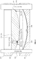
- Fig. 1 shows a flow chart of a method producing an optical element according to an embodiment of the invention.
- the flow chart is explained in connection with Fig. 2 showing a schematical cross-section view of a device 210 for producing the optical element according to a method according to Fig. 1 at one method step as well as Fig. 3A to Fig. 3D .
- Fig. 3A shows a schematical cross-section view of one mould as first part 211 of the alignment device of the device of Fig. 2 at an earlier method step
- Fig. 3B shows a schematical cross-section view of another mould being the second part 212 of the alignment device 210 of Fig. 2 at an earlier method step
- Fig. 3C shows the mould 212 of Fig.
- Fig. 3D shows the device 210 of Fig. 2 at a later method step.
- the first and second parts 211 and 212, respectively, as first and second parts of the alignment device are only used for the alignment.
- the lenses are cast with different (glass) moulds. These parts are therefore only used to align the flex with the foil.
- the embodiment related to Fig. 1 , 2 and 3A to 3D relates to embedding opto-electronic elements in lenses with a defined position as well as a defined spatial alignment, based on a multi-stage process.
- the position of the opto-electronic element is related to the position in the lens in relationship to a coordinate system of the lens.
- the spatial alignment is related to the main axis and direction of the optical element, e.g. the direction 231 in Fig. 3D .
- the optical element produced according to the method can be used for eye tracking functionality through embedded miniature cameras as well as illuminating elements. These functional elements are called active elements, since they either emit light or detect light.
- Other functional elements can be passive elements as crystals as e.g. diamonds or mirror pieces or gratings, which simply reflect, transmit or diffract light directed on these passive elements. The effect of such passive elements are therefore related based on the position and orientation of e.g. the crystal or diffracting structure.
- One advantage of the method according to the invention is based on the predetermined correct positioning and alignment according to a predefined angle in relationship to the lens geometry.
- Passive functional elements 230 can be mounted directly on the foil 216 and aligned afterwards in an alignment step similar to step 115 explained later through alignment tool with vacuum sleeve 225.
- the following description explicitly allows placement of active and passive functional elements, since a FPCB is involved, provided on the mould 212 opposite to mould 211 supporting the foil 216.
- the method steps of the method without a FPCB are - beside the use of the FPCB as intermediate external contact element provided directly between the functional element 230 and the foil 216 - identical.
- the method as shown in Fig. 1 starts with a foil-forming step 111, within which a foil 216 is formed to match the curvature of the lens.
- the mould 211 can comprise one or more through going holes (not shown, from the flat exterior surface towards the concave surface in Fig. 3A ) to hold the foil 216 through applying vacuum from the back side or the mould 211 can be made out of a micro-porous air permeable aluminium compound material as e.g. Metapor ® to allow applying vacuum through the entire back side of the mould 211.
- the next step in the method relates to mounting the functional elements on a flexible printed circuit board (FPCB).
- This step 112 mentions functional elements, which could be electronic elements such as cameras and/or LEDs as active elements.
- Fig. 3B shows the mould 212 as second tool in the cross sectional view
- Fig. 3C shows the mould 212 from above with the foil path 221 for the FPCB portion 221' to be positioned on its surface.
- the mould 212 comprises here an elliptic recess 217 on the outside convex surface, which recess 217 comprises here six contacts having received the reference numeral 222 for the smaller contact plates 222 and 223 for the larger contact plates.
- the elliptic shape of elliptic recess 217 is chosen to provide a closed recess around the center of the lens to be produced. It is possible to have a non-closed shape as a C and it is possible to have a square shape, if the glass to be produced is also essentially square.
- the recesses 217 are complimentary to the form of the flexible printed circuit board 220 to be positioned on the surface and in the recesses and they are preferably fitting the design of the frame of the eye-wear to be near the edge of the frame but inside the frame of the eye wear.
- At the position of the opto-electronic elements at least one through-going hole 215 is prepared in mould 212 to fix the flexible printed circuit board 220 by means of vacuum from the opposite side of the tool mould 212.
- the second mould 212 can comprise the same alignment pin bores 214 as the first mould 211 to precisely align on one side the flexible printed circuit board 220 with the opto-electronic elements 230 with respect to the foil 216 and the second mould 212 face to the first mould 211 as shown in Fig. 2 .
- a second alignment tool is used to execute the method step 115 with an alignment of the camera or cameras and LEDs in the mould to fix the camera(s) at a specific position and angle.
- Method step 114 is related to applying a cut-out around the cameras 230 by using a die cutting tool from the foil. This step can be performed earlier in the process sequence. It can be seen in Fig. 3D that the foil 216, in the cross section view, is interrupted at the cutting edge 227. The cut-out around the camera 230 can have the shape of a C so that the camera 230 is positioned on the flap remaining attached to the foil 216 at line 228 (perpendicular to the drawing plan). Positioned on the sleeve 225 of the second camera alignment tool, the camera 230 can be angled by passively aligning the cut-out of the foil while holding the formed foil 216 with vacuum in place as shown in Fig. 3D . This is done preferably by holding the foil cut-out with a rubber tip, known e.g. from die bonding pick up tools, aligned at the desired angle.
- a rubber tip known e.g. from die bonding pick up tools
- the flexible conductor 221 can be positioned in the according recess and the cameras/LEDs are placed in the vacuum bore holes to attach the flex on the foil.
- Fig. 3D shows the second alignment tool provided in the mould 211.
- the alignment tool comprises a vacuum sleeve 225 applied in a passage 226, which passage can by itself under a separate vacuum to maintain flexible printed circuit board 220 with camera 230 at the correct side. Movement of the vacuum sleeve 225 is effected with an applied internal vacuum and positions and orients the camera 230 and its central axis 231. The axis 231 is oriented as well as the position of the base of the camera 230 chip. Then a liquid adhesive medium e.g. an index matched UV-curable adhesive is added at spot 232 especially around the camera 230 on the border edge of the above mentioned e.g.
- a liquid adhesive medium e.g. an index matched UV-curable adhesive is added at spot 232 especially around the camera 230 on the border edge of the above mentioned e.g.
- this method step 116 is followed by embedding method step 117, wherein the foil 216 with the attached aligned opto-electronic element(s), as e.g. camera 230, LEDs or passive elements, is mounted to the front of a back mould at a defined distance.
- Fig. 3D shows the foil on first mould 211 but it is also possible that the foil 216 is positioned in a distance from the mould 211 in order to obtain better orientation of such a camera.
- the foil is actually mounted on the back of a front mould at a defined distance with the naked foil side facing to the front mould, but both cases are possible.
- the mould cavity itself is formed by aligning front and back mould 211 and 212, i.e. first and second mould, with the attached foil 216 by applying a tape or gasket to seal the mould cavity when the usual production step 118 follows, wherein the mould cavity is filled with curable resin and cured e.g. by applying UV-irradiation or heat.
- Fig. 3D the foil is on the alignment tool with the aligned camera in its fixed position.
- the foil is then fixed on a(nother) glass mould e.g. by applying the foil fixation method of WO 2018/087011 .
- Fig. 4 shows a flow chart of a further method producing an optical element according to an embodiment of the invention.
- the flow chart is explained in connection with Fig. 5 showing a schematical cross-section view of a device 310 for producing the optical element according to a method according to Fig. 4 at one method step, wherein Fig. 6 shows the device 310 of Fig. 5 at a later method step and Fig. 7 shows a detail view of the device 310 of Fig. 6 .
- the method according to the flowchart of Fig. 4 is related to a passive alignment of cameras, wherein a FPCB 353 can be used as substrate for the attachment of the opto-electronic elements by applying printable connectors.
- the printable connector of this embodiment is then attached to a prism 350.
- step 313 comprises positioning of the FPCB 353 with the camera 230 in the corresponding opening 351 which is a vacuum channel having a front part enclosing the camera 230 with play avoiding imposing a specific orientation of camera 230.
- the front part of the vacuum channel 351 is an indentation 352 with a central hole to steadily apply suction on the camera 230 in the indentation to maintain it prior to fixation in a still orientable way.
- the camera 230 can be angled applying a cut out as explained in connection with Fig. 1 to 3D or by using the wedge or prism 350.
- the camera 230 can be aligned and electrically connected applying a part produced by e.g. MID Technology (moulded interconnect device technology). That allows producing miniature conductive elements with a high degree of freedom regarding the 3D design. It is the outer surface and angle of the prism which determines the orientation of the camera. Therefore, the method used in connection with Fig. 5 is a passive method.
- Fig. 7 shows the mounted FPCB 353 with camera 230 on prism 350.
- the FPCB 353 portion is flexible enough to adopt the contour surface of prism 350.
- the thickness of the FPCB 353 is exaggerated to better show this specific element. Since the thickness is constant at the attachment of the camera 230, the camera adopts the orientation of the prism 350 and inherits the position on the prism. This means that corner 354, better the folding line at the edge of the prism 350 is not necessarily the folding line as shown in Fig. 5 but will be determined by the positioning of the camera 230 on the side surface of the prism and will follow the form of the prism 350.
- the realization with the FPCB is shown with the wedge instead of cut-out, but this wedge method could also be combined with the printed conductor instead of the shown FPCB.
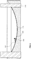
- Fig. 8 shows a flow chart of a method producing an optical element according to a further embodiment of the invention, which is explained in connection with Fig. 9 showing a schematical cross-section view of a further device 410 for producing the optical element according to the method according to Fig. 8 at a specific method step.
- the foil forming step 111 to match the curvature of the lens is preceded by two further steps.
- One step 411 is related to printing the conductors on a flat foil, e.g. by screen printing and curing the conductors.
- the second step 412 is related to mounting of optoelectronic elements such as cameras 230 and/or LEDs on the prepared flat foil with conductors.
- a cut-out is created in the foil for a flap with the camera mounted thereon and a following positioning and alignment procedure with the alignment tool or the element as camera 230 is placed on the wedge or prism wherein the conductors can be e.g. applied according to MID Technology to conform to the additional form of the prism 350 allowing for direct alignment of the camera on the wedge.
- Fig. 9 shows an active alignment tool 420 with alignment reference structure 423 being e.g. an LED array used for adjusting the position and angle of the camera 230 by a vacuum tool 225.
- the camera 230 is connected to the supply unit and the camera 230 is used to align it by evaluating the image of the reference structure 423 which will change following change of position and orientation of camera 230.
- the arrows 421 and 422 represent micrometre screws which are positioned at the vacuum channel 225 in order to displace it against the flexible printed circuit board with the attached camera 230 which is then aligned in a different way towards the reference structure 423.
- Reference numeral 421 represents tilting and rotation of the camera, while reference numeral 422 represents a linear positioning movement.
- Fig. 10 shows a further device 410, wherein the alignment tool comprises a micrometer screw device 420 which provide the lateral displacement 422 as well as the rotation and tilting 421 as indicated in Fig. 9 .
- LIST OF REFERENCE SIGNS 111 foil forming step 223 further FPCB contact 112 functional element mounting 225 vacuum sleeve step on FPCB 226 passage 113 alignment and fixation of 227 cutting edge FPCB 228 foil flap / cut-out 114 cut-out of camera 230 camera 115 alignment of camera 231 central axis 116 fixation of aligned camera 232 liquid adhesive spot 117 positioning of foil with 310 device functional element in mould 313 positioning of prism 118 filling of mould with polymer 314 positioning step and curing of polymer 315 foil mounting step 210 device 350 prism 211 first mould 351 vacuum channel 212 second mould 352 indention with central hole 213 alignment pin 353 printed connector 214 alignment bore 354 corner 215 vacuum channel 410 device 216 foil 411 printing conduct
Landscapes
- Engineering & Computer Science (AREA)
- Mechanical Engineering (AREA)
- Health & Medical Sciences (AREA)
- Manufacturing & Machinery (AREA)
- Ophthalmology & Optometry (AREA)
- Physics & Mathematics (AREA)
- Microelectronics & Electronic Packaging (AREA)
- Signal Processing (AREA)
- Multimedia (AREA)
- General Physics & Mathematics (AREA)
- Optics & Photonics (AREA)
- Thermal Sciences (AREA)
- Oral & Maxillofacial Surgery (AREA)
- Studio Devices (AREA)
- Led Device Packages (AREA)
- Camera Bodies And Camera Details Or Accessories (AREA)
- Mounting And Adjusting Of Optical Elements (AREA)
- Eyeglasses (AREA)
- Light Receiving Elements (AREA)
Description
- The present invention relates to a method for mounting functional elements in a lens.
- Miniaturization of cameras and other optical elements provide fields for new applications relating to the vision of users.
-
US 2015/0009309 shows an optical frame for glasses with an build-in camera and an actuator for said camera. The camera is positioned on the frame outside of the lenses. -
US 2017/0090564 discloses systems and methods for providing a display of a wearable device and is related to elements for an eye-tracking device. Such devices need illumination; usually provided by LEDs and cameras directed towards the eye for determining the gaze. It is disclosed that the illuminating elements can be provided on or in a lens of glasses. These LEDs as well as sensors for sensing the light reflected from an illuminated eye can be provided on flexible printed circuits which are oriented to minimize the visible profile thereof. -
WO 2006/091873 shows manufacturing methods for embedded optical systems, wherein different optical elements as mirrors, etc. are integrated within a glass body being prepared by providing a mould assembly, attaching the optical elements to a wall of the mould cavity and introducing an optical polymerizable casting compound into the mould cavity to obtain the optical component after curing. -
WO 2015/162498 discloses an eyewear lens production using multi-layer additive techniques, where radiation polymerizable material is applied to the lens substrate and irradiated later on with controlled radiation so that an additive layer is formed at the selected irradiated areas according to the intended layer design. -
EP 2 848 979 provides disclosure for different methods and apparatuses for providing variable optic inserts into ophthalmic lenses. -
US 2017/0074494 provides over-moulded LEDs in virtual reality headsets. -
US 2014/273316 A1 discloses methods and apparatus to form organic semiconductor transistors upon three-dimensionally formed insert devices. The three-dimensional surfaces incorporate with organic semiconductor-based thin film transistors, electrical interconnects, and energization elements into an insert for incorporation into ophthalmic lenses. The formed insert may be directly used as an ophthalmic device or incorporated into an ophthalmic device. -
US 9,636,050 B1 - Based on the prior art it is an object of the invention to provide an improved method for placing and orienting functional elements in lenses. Such functional elements can be light sources as LED's and miniature cameras as well as passive functional elements as crystals, e.g. diamonds or other light reflecting or diffracting elements as mirrors or gratings. The present invention relates to methods for mounting functional elements in a lens according to independent claims 1, 2 and 9.
- Such a method for mounting functional elements in a lens comprises the steps of: mounting the functional elements on a foil, applying a closed contour alignment surface of an alignment tool having a central opening surrounded by the closed contour on the foil portion opposite to the mounted function elements, applying underpressure on the central opening to maintain the foil portion with the mounted functional elements on the alignment tool, cutting a flap comprising the foil portion and supporting the functional elements out of the foil, positioning and aligning the flap through actuators, fixing the position of the flap against the adjacent foil surface, embedding the foil with the mounted functional elements in a predetermined distance to the front surface of a casting mould, and casting and curing the lens with the embedded foil. Here, no specific FPCB is provided on the mould opposite to the mould supporting the foil and having the central opening for positioning and aligning the functional elements in view of the foil. Then passive functional elements can be contacted directly and active functional elements are to be contacted through the foil portion, e.g. by contact elements passing through the foil.
- The step of mounting the functional element on a foil can be preceded by placing the functional element on a flexible printed circuit board (FPCB) and affix it there. The flexible printed circuit board can be provided near and at the edges of the lens to be fabricated and comprise contact plates for active functional elements as cameras and light sources as LEDs. Then the method for mounting functional elements in a lens comprises the steps of: mounting the functional elements on a FPCB and affix it there, mounting the FPCB with the affixed functional elements on a foil and affix it there, applying a closed contour alignment surface of an alignment tool having a central opening surrounded by the closed contour on the foil portion opposite to the mounted function elements, applying underpressure on the central opening to maintain the foil portion with the mounted functional elements on the alignment tool, cutting a hole in the foil portion with the functional elements supported by the FPCB or cutting a flap comprising the foil portion and the functional elements supported by the FPCB out of the foil, respectively, positioning and aligning the functional elements supported by the FPCB on the cut-out foil portion or the flap with the functional elements supported by the FPCB through actuators, respectively, fixing the position of the cut-out foil portion with the functional elements on the FPCB or the position of the flap against the adjacent foil surface, embedding the foil with the mounted functional elements on the FPCB in a predetermined distance to the front surface of a casting mould, and casting and curing the lens with the embedded foil.
- The method can have a step of placing the functional element on a flexible printed board circuit and affix it there with positioning the flexible printed board circuit on the surface of a mould, especially in complementary recesses, and applying underpressure from the mould side through at least one vacuum channel in the mould, wherein the functional element is positioned by a functional element alignment tool through the vacuum channel on the flexible printed board circuit.
- A further method for mounting functional elements in a lens comprises the steps of mounting a functional element on a flexible printed board circuit, providing an alignment element on a foil having a predetermined mounting surface for the functional element, positioning the functional element on the alignment element, fixing the position of the functional element on the alignment element, embedding the foil with the mounted functional elements in a predetermined distance to the front surface of a mould, and casting and curing the lens with the embedded foil.
- Mounting a functional element on a flexible printed circuit board can comprise providing a vacuum channel in a mould holding the flexible printed circuit board and within which vacuum channel the functional element is held with play before being positioned on the alignment element.
- The functional element to be placed can comprise at least one camera or a light emitting element or a passive element.
- When the functional element to be placed comprises at least one camera, then the alignment step comprises connecting the camera to a visualizing unit and providing a light source emitting light in a predetermined direction and positioning and aligning the camera based on the images obtained on the visualizing unit from the camera.
- When the functional element to be placed comprises at least one light source, then the alignment step comprises providing a camera and a visualizing unit, wherein the camera receives light from the light source, and positioning and aligning the light source is based on the images obtained on the visualizing unit from the camera.
- Finally, when the functional element to be placed comprises a passive element reflecting or diffracting incoming light, then the alignment step comprises providing a light source, a camera and a visualizing unit, wherein the camera receives light from the passive element illuminated by the light source, and positioning and aligning the passive element is based on the images obtained on the visualizing unit from the camera.
- Further embodiments of the invention are laid down in the dependent claims.
- Preferred embodiments of the invention are described in the following with reference to the drawings, which are for the purpose of illustrating the present preferred embodiments of the invention and not for the purpose of limiting the same. In the drawings,
- Fig. 1
- shows a flow chart of a method producing an optical element according to an embodiment of the invention;
- Fig. 2
- shows a schematical cross-section view of a device for producing the optical element according to a method according to
Fig. 1 during one of the method steps; - Fig. 3A
- shows a schematical cross-section view of one mould of the device of
Fig. 2 at an earlier method step; - Fig. 3B
- shows a schematical cross-section view of a further mould of the device of
Fig. 2 at an earlier method step; - Fig. 3C
- shows the mould of
Fig. 3B in a view from above; - Fig. 3D
- shows the device of
Fig. 2 at a later method step; - Fig. 4
- shows a flow chart of a further method producing an optical element according to an embodiment of the invention;
- Fig. 5
- shows a schematical cross-section view of a device for producing the optical element according to a method according to
Fig. 4 at one method step; - Fig. 6
- shows the device of
Fig. 5 at a later method step; - Fig. 7
- shows a detail view of the device of
Fig. 6 ; - Fig. 8
- shows a flow chart of a method producing an optical element according to an embodiment of the invention;
- Fig. 9
- shows a schematical cross-section view of a device for producing the optical element according to a method according to
Fig. 8 at one method step, and - Fig. 10
- shows a schematical cross-section view of a further device for producing the optical element according to a method according to
Fig. 8 at one method step. -
Fig. 1 shows a flow chart of a method producing an optical element according to an embodiment of the invention. The flow chart is explained in connection withFig. 2 showing a schematical cross-section view of adevice 210 for producing the optical element according to a method according toFig. 1 at one method step as well asFig. 3A to Fig. 3D .Fig. 3A shows a schematical cross-section view of one mould asfirst part 211 of the alignment device of the device ofFig. 2 at an earlier method step,Fig. 3B shows a schematical cross-section view of another mould being thesecond part 212 of thealignment device 210 ofFig. 2 at an earlier method step,Fig. 3C shows themould 212 ofFig. 3A in a view from above, andFig. 3D shows thedevice 210 ofFig. 2 at a later method step. The first andsecond parts Fig. 1 ,2 and3A to 3D relates to embedding opto-electronic elements in lenses with a defined position as well as a defined spatial alignment, based on a multi-stage process. The position of the opto-electronic element is related to the position in the lens in relationship to a coordinate system of the lens. The spatial alignment is related to the main axis and direction of the optical element, e.g. thedirection 231 inFig. 3D . The optical element produced according to the method can be used for eye tracking functionality through embedded miniature cameras as well as illuminating elements. These functional elements are called active elements, since they either emit light or detect light. Other functional elements can be passive elements as crystals as e.g. diamonds or mirror pieces or gratings, which simply reflect, transmit or diffract light directed on these passive elements. The effect of such passive elements are therefore related based on the position and orientation of e.g. the crystal or diffracting structure. - One advantage of the method according to the invention is based on the predetermined correct positioning and alignment according to a predefined angle in relationship to the lens geometry. Passive
functional elements 230 can be mounted directly on thefoil 216 and aligned afterwards in an alignment step similar to step 115 explained later through alignment tool withvacuum sleeve 225. The following description explicitly allows placement of active and passive functional elements, since a FPCB is involved, provided on themould 212 opposite tomould 211 supporting thefoil 216. The method steps of the method without a FPCB are - beside the use of the FPCB as intermediate external contact element provided directly between thefunctional element 230 and the foil 216 - identical. - The method as shown in
Fig. 1 starts with a foil-formingstep 111, within which afoil 216 is formed to match the curvature of the lens. Themould 211 can comprise one or more through going holes (not shown, from the flat exterior surface towards the concave surface inFig. 3A ) to hold thefoil 216 through applying vacuum from the back side or themould 211 can be made out of a micro-porous air permeable aluminium compound material as e.g. Metapor® to allow applying vacuum through the entire back side of themould 211. - The next step in the method relates to mounting the functional elements on a flexible printed circuit board (FPCB). This
step 112 mentions functional elements, which could be electronic elements such as cameras and/or LEDs as active elements.Fig. 3B shows themould 212 as second tool in the cross sectional view, whereasFig. 3C shows themould 212 from above with thefoil path 221 for the FPCB portion 221' to be positioned on its surface. As shown inFig. 3C , themould 212 comprises here anelliptic recess 217 on the outside convex surface, whichrecess 217 comprises here six contacts having received thereference numeral 222 for thesmaller contact plates 222 and 223 for the larger contact plates. The elliptic shape ofelliptic recess 217 is chosen to provide a closed recess around the center of the lens to be produced. It is possible to have a non-closed shape as a C and it is possible to have a square shape, if the glass to be produced is also essentially square. Therecesses 217 are complimentary to the form of the flexible printedcircuit board 220 to be positioned on the surface and in the recesses and they are preferably fitting the design of the frame of the eye-wear to be near the edge of the frame but inside the frame of the eye wear. - At the position of the opto-electronic elements at least one through-going
hole 215 is prepared inmould 212 to fix the flexible printedcircuit board 220 by means of vacuum from the opposite side of thetool mould 212. Thesecond mould 212 can comprise the same alignment pin bores 214 as thefirst mould 211 to precisely align on one side the flexible printedcircuit board 220 with the opto-electronic elements 230 with respect to thefoil 216 and thesecond mould 212 face to thefirst mould 211 as shown inFig. 2 . A second alignment tool, not shown in this drawing, is used to execute themethod step 115 with an alignment of the camera or cameras and LEDs in the mould to fix the camera(s) at a specific position and angle. -
Method step 114 is related to applying a cut-out around thecameras 230 by using a die cutting tool from the foil. This step can be performed earlier in the process sequence. It can be seen inFig. 3D that thefoil 216, in the cross section view, is interrupted at thecutting edge 227. The cut-out around thecamera 230 can have the shape of a C so that thecamera 230 is positioned on the flap remaining attached to thefoil 216 at line 228 (perpendicular to the drawing plan). Positioned on thesleeve 225 of the second camera alignment tool, thecamera 230 can be angled by passively aligning the cut-out of the foil while holding the formedfoil 216 with vacuum in place as shown inFig. 3D . This is done preferably by holding the foil cut-out with a rubber tip, known e.g. from die bonding pick up tools, aligned at the desired angle. - The
flexible conductor 221 can be positioned in the according recess and the cameras/LEDs are placed in the vacuum bore holes to attach the flex on the foil. -
Fig. 3D shows the second alignment tool provided in themould 211. The alignment tool comprises avacuum sleeve 225 applied in apassage 226, which passage can by itself under a separate vacuum to maintain flexible printedcircuit board 220 withcamera 230 at the correct side. Movement of thevacuum sleeve 225 is effected with an applied internal vacuum and positions and orients thecamera 230 and itscentral axis 231. Theaxis 231 is oriented as well as the position of the base of thecamera 230 chip. Then a liquid adhesive medium e.g. an index matched UV-curable adhesive is added atspot 232 especially around thecamera 230 on the border edge of the above mentioned e.g. C-shaped cut-out contour to executemethod step 116, wherein the alignment of thecamera 230 is fixed using said adhesive 232 while the position is still maintained by the second alignment tool with application of a vacuum on thevacuum sleeve 225. If the cut-out contour is C-shaped, then the contour of the adhesive 232 has as such also the shape of the C closing the gap at theedge 227. - Then, this
method step 116 is followed by embeddingmethod step 117, wherein thefoil 216 with the attached aligned opto-electronic element(s), ase.g. camera 230, LEDs or passive elements, is mounted to the front of a back mould at a defined distance.Fig. 3D shows the foil onfirst mould 211 but it is also possible that thefoil 216 is positioned in a distance from themould 211 in order to obtain better orientation of such a camera. Within a different approach, the foil is actually mounted on the back of a front mould at a defined distance with the naked foil side facing to the front mould, but both cases are possible. - Then, the mould cavity itself is formed by aligning front and
back mould foil 216 by applying a tape or gasket to seal the mould cavity when theusual production step 118 follows, wherein the mould cavity is filled with curable resin and cured e.g. by applying UV-irradiation or heat. - In
Fig. 3D the foil is on the alignment tool with the aligned camera in its fixed position. The foil is then fixed on a(nother) glass mould e.g. by applying the foil fixation method ofWO 2018/087011 . -
Fig. 4 then shows a flow chart of a further method producing an optical element according to an embodiment of the invention. The flow chart is explained in connection withFig. 5 showing a schematical cross-section view of adevice 310 for producing the optical element according to a method according toFig. 4 at one method step, whereinFig. 6 shows thedevice 310 ofFig. 5 at a later method step andFig. 7 shows a detail view of thedevice 310 ofFig. 6 . - Same features receive the same reference numerals. This is also true for identical or very similar steps in the method step of
Fig. 2 . - The
initial steps Fig. 1 to 3D . - The method according to the flowchart of
Fig. 4 is related to a passive alignment of cameras, wherein aFPCB 353 can be used as substrate for the attachment of the opto-electronic elements by applying printable connectors. The printable connector of this embodiment is then attached to aprism 350. - In a different approach the printed conductor is printed directly on the surface of the
wedge 350 or it can be printed on theflat foil 216 wherein the surface mount of theoptoelectronic element 230 is done on the printed conductors and finally in step 119 the mould cavity is filled with a curable resin and cured by a UV radiation.Reference numeral 353 would either be a FPCB or - in case printed conductors are used - would be directly placed on the conductor on the wedge (e.g. by MID technology). Here,step 313 comprises positioning of theFPCB 353 with thecamera 230 in thecorresponding opening 351 which is a vacuum channel having a front part enclosing thecamera 230 with play avoiding imposing a specific orientation ofcamera 230. The front part of thevacuum channel 351 is anindentation 352 with a central hole to steadily apply suction on thecamera 230 in the indentation to maintain it prior to fixation in a still orientable way. - The
camera 230 can be angled applying a cut out as explained in connection withFig. 1 to 3D or by using the wedge orprism 350. Here thecamera 230 can be aligned and electrically connected applying a part produced by e.g. MID Technology (moulded interconnect device technology). That allows producing miniature conductive elements with a high degree of freedom regarding the 3D design. It is the outer surface and angle of the prism which determines the orientation of the camera. Therefore, the method used in connection withFig. 5 is a passive method. -
Fig. 7 shows the mountedFPCB 353 withcamera 230 onprism 350. TheFPCB 353 portion is flexible enough to adopt the contour surface ofprism 350. The thickness of theFPCB 353 is exaggerated to better show this specific element. Since the thickness is constant at the attachment of thecamera 230, the camera adopts the orientation of theprism 350 and inherits the position on the prism. This means thatcorner 354, better the folding line at the edge of theprism 350 is not necessarily the folding line as shown inFig. 5 but will be determined by the positioning of thecamera 230 on the side surface of the prism and will follow the form of theprism 350. InFigs. 6 and7 the realization with the FPCB is shown with the wedge instead of cut-out, but this wedge method could also be combined with the printed conductor instead of the shown FPCB. -
Fig. 8 shows a flow chart of a method producing an optical element according to a further embodiment of the invention, which is explained in connection withFig. 9 showing a schematical cross-section view of afurther device 410 for producing the optical element according to the method according toFig. 8 at a specific method step. - Within an alternative process sequence the
foil forming step 111 to match the curvature of the lens is preceded by two further steps. Onestep 411 is related to printing the conductors on a flat foil, e.g. by screen printing and curing the conductors. Thesecond step 412 is related to mounting of optoelectronic elements such ascameras 230 and/or LEDs on the prepared flat foil with conductors. - Then as in the previously described method, in a
positioning step 413, a cut-out is created in the foil for a flap with the camera mounted thereon and a following positioning and alignment procedure with the alignment tool or the element ascamera 230 is placed on the wedge or prism wherein the conductors can be e.g. applied according to MID Technology to conform to the additional form of theprism 350 allowing for direct alignment of the camera on the wedge. - Then the steps of foil embedding 117 and lens casting 118 follow as explained above.
-
Fig. 9 shows anactive alignment tool 420 withalignment reference structure 423 being e.g. an LED array used for adjusting the position and angle of thecamera 230 by avacuum tool 225. Thecamera 230 is connected to the supply unit and thecamera 230 is used to align it by evaluating the image of thereference structure 423 which will change following change of position and orientation ofcamera 230. Thearrows vacuum channel 225 in order to displace it against the flexible printed circuit board with the attachedcamera 230 which is then aligned in a different way towards thereference structure 423.Reference numeral 421 represents tilting and rotation of the camera, whilereference numeral 422 represents a linear positioning movement. -
Fig. 10 shows afurther device 410, wherein the alignment tool comprises amicrometer screw device 420 which provide thelateral displacement 422 as well as the rotation and tilting 421 as indicated inFig. 9 .LIST OF REFERENCE SIGNS 111 foil forming step 223 further FPCB contact 112 functional element mounting 225 vacuum sleeve step on FPCB 226 passage 113 alignment and fixation of 227 cutting edge FPCB 228 foil flap / cut-out 114 cut-out of camera 230 camera 115 alignment of camera 231 central axis 116 fixation of aligned camera 232 liquid adhesive spot 117 positioning of foil with 310 device functional element in mould 313 positioning of prism 118 filling of mould with polymer 314 positioning step and curing of polymer 315 foil mounting step 210 device 350 prism 211 first mould 351 vacuum channel 212 second mould 352 indention with central hole 213 alignment pin 353 printed connector 214 alignment bore 354 corner 215 vacuum channel 410 device 216 foil 411 printing conductors 217 groove 412 mounting electronic elements 218 recess on foil with conductors 220 flexible printed circuit board 413 positioning step 221 hole for opto-electronic 420 alignment tool element 421 rotation actuator 221' FPCB conducting path 422 linear displacement actuator 222 hole for opto- electronic element 423 alignment reference structure
Claims (15)
- A method for mounting functional elements (230) in a lens comprising the steps of:- mounting the functional elements (230) on a foil (216) and affix it there,- applying a closed contour alignment surface of an alignment tool (225) having a central opening surrounded by the closed contour on a foil portion opposite to the mounted function elements (230),- applying underpressure on the central opening to maintain the foil portion with the mounted functional elements (230) on the alignment tool (225),- cutting a hole in the foil portion with the functional elements (230) or cutting a flap (114) comprising the foil portion and the functional elements (230) out of the foil, respectively,- positioning and aligning (115) the functional elements (230) on the cut-out foil portion or the flap (114) with the functional elements (230) through actuators (421, 422), respectively,- fixing (116) the position of the cut-out foil portion with the functional elements (230) or the position of the flap (114) against the adjacent foil surface,- embedding (117) the foil (216) with the mounted functional elements (230) in a predetermined distance to the front surface of a casting mould, and- casting (118) and curing the lens with the embedded foil.
- A method for mounting functional elements (230) in a lens comprising the steps of:- mounting the functional elements (230) on a flexible printed circuit board (220) and affix it there,- mounting the flexible printed circuit board (220) with the affixed functional elements (230) on a foil (216) and affix it there,- applying a closed contour alignment surface of an alignment tool (225) having a central opening surrounded by the closed contour on the foil portion opposite to the mounted function elements (230),- applying underpressure on the central opening to maintain the foil portion with the mounted functional elements (230) on the alignment tool (225),- cutting a hole in the foil portion with the functional elements (230) supported by the flexible printed circuit board (220) or cutting a flap (114) comprising the foil portion and the functional elements (230) supported by the flexible printed circuit board (220) out of the foil, respectively,- positioning and aligning (115) the functional elements (230) supported by the flexible printed circuit board (220) on the cut-out foil portion or the flap (114) with the functional elements (230) supported by the flexible printed circuit board (220) through actuators (421, 422), respectively,- fixing (116) the position of the cut-out foil portion with the functional elements (230) on the flexible printed circuit board (220) or the position of the flap (114) against the adjacent foil surface,- embedding (117) the foil (216) with the mounted functional elements (230) on the flexible printed circuit board (220) in a predetermined distance to the front surface of a casting mould, and- casting (118) and curing the lens with the embedded foil.
- The method according to claim 2, wherein the step of placing the functional element (230) on the flexible printed circuit board and affix it there comprises positioning the flexible printed circuit board on the surface of a mould, especially in complementary recesses, and applying underpressure from the mould side through at least one vacuum channel in the mould, wherein the functional element is positioned by a functional element alignment tool through the vacuum channel on the flexible printed circuit board.
- The method according to any one of claims 1 to 3, wherein the functional element to be placed comprises at least one camera (230) or a light emitting element or a passive element.
- The method according to claim 4, wherein the functional element to be placed comprises at least one camera (230) and the alignment step comprises connecting the camera to a visualizing unit and providing a light delivering source, as a light source emitting light or a simple structure such as a reference grid that is aligned specifically, in a predetermined direction and positioning and aligning the camera based on the images obtained on the visualizing unit from the camera.
- The method according to claim 4, wherein the functional element to be placed comprises at least one light source and the alignment step comprises providing a camera and a visualizing unit, wherein the camera receives light from the light source, and positioning and aligning the light source is based on the images obtained on the visualizing unit from the camera.
- The method according to claim 4, wherein the functional element to be placed comprises a passive element reflecting or diffracting incoming light and wherein the alignment step comprises providing a light source, a camera and a visualizing unit, wherein the camera receives light from the passive element illuminated by the light source, and positioning and aligning the passive element is based on the images obtained on the visualizing unit from the camera.
- The method according to claim 7, wherein the passive element is a crystal, a mirror element or a grating.
- A method for mounting functional elements (230) in a lens comprising the steps of:- providing an alignment element (350) on a foil (216) having a predetermined mounting surface for the functional element (230),- positioning the functional element (230) on the alignment element (350),- fixing (116) the position of the functional element (230) on the alignment element (350),- embedding (117) the foil (216) with the mounted functional elements (230) in a predetermined distance to the front surface of a mould (212), and- casting (118) and curing the lens with the embedded foil.
- The method according to claim 9, including the step of initially mounting a functional element (230) on a flexible printed circuit board.
- The method according to claim 9 or 10, wherein mounting a functional element (230) on a flexible printed board circuit comprises providing a vacuum channel in a mould holding the flexible printed circuit board and within which vacuum channel the functional element is held with play before being positioned on the alignment element (350).
- The method according to any of claims 9 to 11, wherein the functional element to be placed comprises at least one camera (230) or a light emitting element or a passive element.
- The method according to claim 12, wherein the functional element to be placed comprises at least one camera (230) and wherein the method comprises connecting the camera to a visualizing unit and providing a light delivering source, as a light source emitting light or a simple structure such as a reference grid that is aligned specifically, in a predetermined direction and positioning and aligning the camera based on the images obtained on the visualizing unit from the camera.
- The method according to claim 12, wherein the functional element to be placed comprises at least one light source and wherein the method comprises providing a camera and a visualizing unit, wherein the camera receives light from the light source, and positioning and aligning the light source based on the images obtained on the visualizing unit from the camera.
- The method according to claim 12, wherein the functional element to be placed comprises a passive element reflecting or diffracting incoming light and wherein the method comprises providing a light source, a camera and a visualizing unit, wherein the camera receives light from the passive element illuminated by the light source, and positioning and aligning the passive element based on the images obtained on the visualizing unit from the camera.
Applications Claiming Priority (3)
| Application Number | Priority Date | Filing Date | Title |
|---|---|---|---|
| CH11672018 | 2018-09-25 | ||
| EP18214660.5A EP3670162A1 (en) | 2018-12-20 | 2018-12-20 | Method for mounting functional elements in a lens and device therefor |
| PCT/EP2019/075939 WO2020064879A1 (en) | 2018-09-25 | 2019-09-25 | Method for mounting functional elements in a lens |
Publications (2)
| Publication Number | Publication Date |
|---|---|
| EP3856502A1 EP3856502A1 (en) | 2021-08-04 |
| EP3856502B1 true EP3856502B1 (en) | 2022-10-12 |
Family
ID=68470455
Family Applications (1)
| Application Number | Title | Priority Date | Filing Date |
|---|---|---|---|
| EP19798537.7A Active EP3856502B1 (en) | 2018-09-25 | 2019-09-25 | Method for mounting functional elements in a lens |
Country Status (8)
| Country | Link |
|---|---|
| US (2) | US11697257B2 (en) |
| EP (1) | EP3856502B1 (en) |
| JP (1) | JP2022502708A (en) |
| KR (1) | KR20210086613A (en) |
| CN (1) | CN113260498B (en) |
| CA (1) | CA3114306A1 (en) |
| ES (1) | ES2930442T3 (en) |
| WO (1) | WO2020064879A1 (en) |
Families Citing this family (5)
| Publication number | Priority date | Publication date | Assignee | Title |
|---|---|---|---|---|
| KR20210086613A (en) * | 2018-09-25 | 2021-07-08 | 메타머티리얼 아이앤씨. | How to mount a plurality of functional elements on a lens |
| EP4267380A1 (en) | 2020-12-24 | 2023-11-01 | Luxottica S.r.l. | Eyeglass lens with decorative element |
| EP4237218B1 (en) * | 2021-01-21 | 2024-03-20 | Tobii AB | Improvements relating to lenses |
| US20250236080A1 (en) * | 2022-04-21 | 2025-07-24 | Addoptics B.V. | Method of manufacturing a mould for an optical element |
| CN117103557B (en) * | 2023-07-13 | 2026-04-17 | 荣谕科技(成都)有限公司 | Method for manufacturing eye-tracking glasses |
Family Cites Families (27)
| Publication number | Priority date | Publication date | Assignee | Title |
|---|---|---|---|---|
| WO1999023524A1 (en) * | 1997-10-30 | 1999-05-14 | The Microoptical Corporation | Eyeglass interface system |
| US6986579B2 (en) * | 1999-07-02 | 2006-01-17 | E-Vision, Llc | Method of manufacturing an electro-active lens |
| FR2871586B1 (en) * | 2004-06-11 | 2006-09-29 | Essilor Int | OPHTHALMIC GLASS WITH ELECTRO-OPTICAL FUNCTION |
| US20060192306A1 (en) | 2005-02-25 | 2006-08-31 | The Microoptical Corporation | Manufacturing methods for embedded optical system |
| US20070069418A1 (en) * | 2005-09-28 | 2007-03-29 | Chih-Yuan Liao | In mold manufacturing of an object comprising a functional element |
| JP4828932B2 (en) * | 2005-12-22 | 2011-11-30 | 伊藤光学工業株式会社 | Mold and method for polarizing plastic lens |
| WO2008051578A2 (en) | 2006-10-25 | 2008-05-02 | Volk Donald A | Multi-layered multifocal lens with blended refractive index |
| NL1034496C2 (en) | 2007-10-10 | 2009-04-16 | Anteryon B V | Method for manufacturing an assembly of lenses, as well as a camera provided with such an assembly. |
| CN102548725A (en) * | 2009-09-24 | 2012-07-04 | 旭硝子株式会社 | Mold release film and method for manufacturing light emitting diode |
| US8348461B2 (en) * | 2009-10-30 | 2013-01-08 | Ruud Lighting, Inc. | LED apparatus and method for accurate lens alignment |
| WO2011124764A1 (en) * | 2010-04-06 | 2011-10-13 | Oy Ics Intelligent Control Systems Ltd | Laminate structure with embedded cavities for use with solar cells and related method of manufacture |
| US20150009309A1 (en) | 2011-07-08 | 2015-01-08 | Google Inc. | Optical Frame for Glasses and the Like with Built-In Camera and Special Actuator Feature |
| WO2014077338A1 (en) * | 2012-11-14 | 2014-05-22 | ホーヤ レンズ マニュファクチャリング フィリピン インク | Method for manuf acturing polarizing plastic lens |
| US8894201B2 (en) | 2013-03-15 | 2014-11-25 | Johnson & Johnson Vision Care, Inc. | Methods and ophthalmic devices with thin film transistors |
| CH708048A2 (en) | 2013-05-13 | 2014-11-14 | Abatek Internat Ag | Officials with key functions. |
| SG10201405242WA (en) | 2013-09-17 | 2015-04-29 | Johnson & Johnson Vision Care | Variable optic ophthalmic device including liquid crystal elements |
| US9636050B1 (en) | 2013-11-07 | 2017-05-02 | Verily Life Sciences Llc | Methods and apparatus for forming a channel through a polymer layer using a protrusion |
| US9782942B2 (en) | 2013-12-30 | 2017-10-10 | Verily Life Sciences Llc | Methods and apparatus for positioning a structure on a polymer layer |
| EP3120181B1 (en) | 2014-03-18 | 2025-05-07 | Essilor International | A process for manufacturing an ophthalmic lens equipped with an insert |
| US10816827B2 (en) * | 2014-03-19 | 2020-10-27 | Essilor International | Process for manufacturing an ophthalmic lens equipped with an insert |
| US9933632B2 (en) | 2014-03-26 | 2018-04-03 | Indizen Optical Technologies, S.L. | Eyewear lens production by multi-layer additive techniques |
| CH709485B1 (en) | 2014-04-11 | 2018-07-13 | Interglass Tech Ag | Method for producing a lens by casting. |
| US9535254B2 (en) | 2014-12-31 | 2017-01-03 | Oculus Vr, Llc | Overmolded LEDs and fabric in virtual reality headsets |
| TWI698326B (en) * | 2015-01-14 | 2020-07-11 | 德商科思創德意志股份有限公司 | Process for producing an optical casting with a holographic optical element and optical casting |
| CN114035685B (en) | 2015-09-24 | 2024-11-22 | 托比股份公司 | Wearable devices capable of eye tracking |
| KR102487334B1 (en) * | 2016-11-03 | 2023-01-10 | 메타머티리얼 아이앤씨. | Method for manufacturing lenses with embedded foils |
| KR20210086613A (en) * | 2018-09-25 | 2021-07-08 | 메타머티리얼 아이앤씨. | How to mount a plurality of functional elements on a lens |
-
2019
- 2019-09-25 KR KR1020217010102A patent/KR20210086613A/en not_active Ceased
- 2019-09-25 EP EP19798537.7A patent/EP3856502B1/en active Active
- 2019-09-25 ES ES19798537T patent/ES2930442T3/en active Active
- 2019-09-25 US US17/280,166 patent/US11697257B2/en active Active
- 2019-09-25 WO PCT/EP2019/075939 patent/WO2020064879A1/en not_active Ceased
- 2019-09-25 JP JP2021517863A patent/JP2022502708A/en active Pending
- 2019-09-25 CA CA3114306A patent/CA3114306A1/en active Pending
- 2019-09-25 CN CN201980063169.2A patent/CN113260498B/en active Active
-
2023
- 2023-05-15 US US18/197,270 patent/US20230278301A1/en not_active Abandoned
Also Published As
| Publication number | Publication date |
|---|---|
| ES2930442T3 (en) | 2022-12-13 |
| WO2020064879A1 (en) | 2020-04-02 |
| CA3114306A1 (en) | 2020-04-02 |
| KR20210086613A (en) | 2021-07-08 |
| CN113260498A (en) | 2021-08-13 |
| US11697257B2 (en) | 2023-07-11 |
| CN113260498B (en) | 2023-03-21 |
| JP2022502708A (en) | 2022-01-11 |
| EP3856502A1 (en) | 2021-08-04 |
| US20230278301A1 (en) | 2023-09-07 |
| US20210339490A1 (en) | 2021-11-04 |
Similar Documents
| Publication | Publication Date | Title |
|---|---|---|
| US20230278301A1 (en) | Method for mounting functional elements in a lens | |
| US7141450B2 (en) | Flip-chip alignment method | |
| JP5601000B2 (en) | Imaging device | |
| RU2616757C2 (en) | Method of making lightguide device, lightguide device and virtual images mapping device | |
| CN107277316B (en) | Display device and method of manufacturing the same | |
| US20120086784A1 (en) | Three dimensional image pick-up device and manufacturing method thereof | |
| EP2808912B1 (en) | Method for assembling a circuit carrier with a housing component, and an optical unit | |
| CN102741729B (en) | A method of manufacturing a lens for providing an optical display | |
| US20210132384A1 (en) | Tilted In-Field Light Sources | |
| KR20240068647A (en) | Spectacle lenses with eye tracking components | |
| EP3670162A1 (en) | Method for mounting functional elements in a lens and device therefor | |
| CN106132675B (en) | Method for manufacturing an ophthalmic lens equipped with an insert, intermediate product and ophthalmic lens element | |
| EP3371649B1 (en) | Microdisplay module having a reduced size | |
| HK40059511A (en) | Method for mounting functional elements in a lens | |
| EP3376099A1 (en) | Led lighting arrangement | |
| JP2007005494A (en) | Component mounting apparatus, component mounting method, position adjusting apparatus, and position adjusting method | |
| CN119008788A (en) | Optical module and processing method thereof | |
| CN118584699A (en) | Eye tracking glasses | |
| JP2004201328A (en) | Image sensor positioning system and method | |
| JP2009182381A (en) | Imaging module | |
| JP4467656B2 (en) | Focus detection apparatus and position adjustment method | |
| TWI475276B (en) | Optical sub-assembly and packaging method thereof | |
| GB2309796A (en) | Surface mount module and production method thereof | |
| US20250321414A1 (en) | Semiconductor device mounted on a system board | |
| CN116980725B (en) | Camera module with illumination function |
Legal Events
| Date | Code | Title | Description |
|---|---|---|---|
| STAA | Information on the status of an ep patent application or granted ep patent |
Free format text: STATUS: UNKNOWN |
|
| STAA | Information on the status of an ep patent application or granted ep patent |
Free format text: STATUS: THE INTERNATIONAL PUBLICATION HAS BEEN MADE |
|
| PUAI | Public reference made under article 153(3) epc to a published international application that has entered the european phase |
Free format text: ORIGINAL CODE: 0009012 |
|
| STAA | Information on the status of an ep patent application or granted ep patent |
Free format text: STATUS: REQUEST FOR EXAMINATION WAS MADE |
|
| 17P | Request for examination filed |
Effective date: 20210420 |
|
| AK | Designated contracting states |
Kind code of ref document: A1 Designated state(s): AL AT BE BG CH CY CZ DE DK EE ES FI FR GB GR HR HU IE IS IT LI LT LU LV MC MK MT NL NO PL PT RO RS SE SI SK SM TR |
|
| DAV | Request for validation of the european patent (deleted) | ||
| DAX | Request for extension of the european patent (deleted) | ||
| REG | Reference to a national code |
Ref country code: DE Ref legal event code: R079 Ref document number: 602019020617 Country of ref document: DE Free format text: PREVIOUS MAIN CLASS: B29D0011000000 Ipc: B29C0039100000 |
|
| RAP3 | Party data changed (applicant data changed or rights of an application transferred) |
Owner name: TOBII AB Owner name: METAMATERIAL INC. |
|
| GRAP | Despatch of communication of intention to grant a patent |
Free format text: ORIGINAL CODE: EPIDOSNIGR1 |
|
| STAA | Information on the status of an ep patent application or granted ep patent |
Free format text: STATUS: GRANT OF PATENT IS INTENDED |
|
| RIC1 | Information provided on ipc code assigned before grant |
Ipc: B29C 39/42 20060101ALI20220331BHEP Ipc: B29D 11/00 20060101ALI20220331BHEP Ipc: B29C 39/10 20060101AFI20220331BHEP |
|
| INTG | Intention to grant announced |
Effective date: 20220422 |
|
| GRAS | Grant fee paid |
Free format text: ORIGINAL CODE: EPIDOSNIGR3 |
|
| GRAA | (expected) grant |
Free format text: ORIGINAL CODE: 0009210 |
|
| STAA | Information on the status of an ep patent application or granted ep patent |
Free format text: STATUS: THE PATENT HAS BEEN GRANTED |
|
| AK | Designated contracting states |
Kind code of ref document: B1 Designated state(s): AL AT BE BG CH CY CZ DE DK EE ES FI FR GB GR HR HU IE IS IT LI LT LU LV MC MK MT NL NO PL PT RO RS SE SI SK SM TR |
|
| REG | Reference to a national code |
Ref country code: GB Ref legal event code: FG4D |
|
| REG | Reference to a national code |
Ref country code: CH Ref legal event code: EP |
|
| REG | Reference to a national code |
Ref country code: DE Ref legal event code: R096 Ref document number: 602019020617 Country of ref document: DE |
|
| REG | Reference to a national code |
Ref country code: IE Ref legal event code: FG4D |
|
| REG | Reference to a national code |
Ref country code: AT Ref legal event code: REF Ref document number: 1523887 Country of ref document: AT Kind code of ref document: T Effective date: 20221115 |
|
| REG | Reference to a national code |
Ref country code: ES Ref legal event code: FG2A Ref document number: 2930442 Country of ref document: ES Kind code of ref document: T3 Effective date: 20221213 |
|
| REG | Reference to a national code |
Ref country code: LT Ref legal event code: MG9D |
|
| REG | Reference to a national code |
Ref country code: NL Ref legal event code: MP Effective date: 20221012 |
|
| REG | Reference to a national code |
Ref country code: AT Ref legal event code: MK05 Ref document number: 1523887 Country of ref document: AT Kind code of ref document: T Effective date: 20221012 |
|
| PG25 | Lapsed in a contracting state [announced via postgrant information from national office to epo] |
Ref country code: NL Free format text: LAPSE BECAUSE OF FAILURE TO SUBMIT A TRANSLATION OF THE DESCRIPTION OR TO PAY THE FEE WITHIN THE PRESCRIBED TIME-LIMIT Effective date: 20221012 |
|
| PG25 | Lapsed in a contracting state [announced via postgrant information from national office to epo] |
Ref country code: SE Free format text: LAPSE BECAUSE OF FAILURE TO SUBMIT A TRANSLATION OF THE DESCRIPTION OR TO PAY THE FEE WITHIN THE PRESCRIBED TIME-LIMIT Effective date: 20221012 Ref country code: PT Free format text: LAPSE BECAUSE OF FAILURE TO SUBMIT A TRANSLATION OF THE DESCRIPTION OR TO PAY THE FEE WITHIN THE PRESCRIBED TIME-LIMIT Effective date: 20230213 Ref country code: NO Free format text: LAPSE BECAUSE OF FAILURE TO SUBMIT A TRANSLATION OF THE DESCRIPTION OR TO PAY THE FEE WITHIN THE PRESCRIBED TIME-LIMIT Effective date: 20230112 Ref country code: LT Free format text: LAPSE BECAUSE OF FAILURE TO SUBMIT A TRANSLATION OF THE DESCRIPTION OR TO PAY THE FEE WITHIN THE PRESCRIBED TIME-LIMIT Effective date: 20221012 Ref country code: FI Free format text: LAPSE BECAUSE OF FAILURE TO SUBMIT A TRANSLATION OF THE DESCRIPTION OR TO PAY THE FEE WITHIN THE PRESCRIBED TIME-LIMIT Effective date: 20221012 Ref country code: AT Free format text: LAPSE BECAUSE OF FAILURE TO SUBMIT A TRANSLATION OF THE DESCRIPTION OR TO PAY THE FEE WITHIN THE PRESCRIBED TIME-LIMIT Effective date: 20221012 |
|
| PG25 | Lapsed in a contracting state [announced via postgrant information from national office to epo] |
Ref country code: RS Free format text: LAPSE BECAUSE OF FAILURE TO SUBMIT A TRANSLATION OF THE DESCRIPTION OR TO PAY THE FEE WITHIN THE PRESCRIBED TIME-LIMIT Effective date: 20221012 Ref country code: PL Free format text: LAPSE BECAUSE OF FAILURE TO SUBMIT A TRANSLATION OF THE DESCRIPTION OR TO PAY THE FEE WITHIN THE PRESCRIBED TIME-LIMIT Effective date: 20221012 Ref country code: LV Free format text: LAPSE BECAUSE OF FAILURE TO SUBMIT A TRANSLATION OF THE DESCRIPTION OR TO PAY THE FEE WITHIN THE PRESCRIBED TIME-LIMIT Effective date: 20221012 Ref country code: IS Free format text: LAPSE BECAUSE OF FAILURE TO SUBMIT A TRANSLATION OF THE DESCRIPTION OR TO PAY THE FEE WITHIN THE PRESCRIBED TIME-LIMIT Effective date: 20230212 Ref country code: HR Free format text: LAPSE BECAUSE OF FAILURE TO SUBMIT A TRANSLATION OF THE DESCRIPTION OR TO PAY THE FEE WITHIN THE PRESCRIBED TIME-LIMIT Effective date: 20221012 Ref country code: GR Free format text: LAPSE BECAUSE OF FAILURE TO SUBMIT A TRANSLATION OF THE DESCRIPTION OR TO PAY THE FEE WITHIN THE PRESCRIBED TIME-LIMIT Effective date: 20230113 |
|
| P01 | Opt-out of the competence of the unified patent court (upc) registered |
Effective date: 20230523 |
|
| REG | Reference to a national code |
Ref country code: DE Ref legal event code: R097 Ref document number: 602019020617 Country of ref document: DE |
|
| PG25 | Lapsed in a contracting state [announced via postgrant information from national office to epo] |
Ref country code: SM Free format text: LAPSE BECAUSE OF FAILURE TO SUBMIT A TRANSLATION OF THE DESCRIPTION OR TO PAY THE FEE WITHIN THE PRESCRIBED TIME-LIMIT Effective date: 20221012 Ref country code: RO Free format text: LAPSE BECAUSE OF FAILURE TO SUBMIT A TRANSLATION OF THE DESCRIPTION OR TO PAY THE FEE WITHIN THE PRESCRIBED TIME-LIMIT Effective date: 20221012 Ref country code: EE Free format text: LAPSE BECAUSE OF FAILURE TO SUBMIT A TRANSLATION OF THE DESCRIPTION OR TO PAY THE FEE WITHIN THE PRESCRIBED TIME-LIMIT Effective date: 20221012 Ref country code: DK Free format text: LAPSE BECAUSE OF FAILURE TO SUBMIT A TRANSLATION OF THE DESCRIPTION OR TO PAY THE FEE WITHIN THE PRESCRIBED TIME-LIMIT Effective date: 20221012 Ref country code: CZ Free format text: LAPSE BECAUSE OF FAILURE TO SUBMIT A TRANSLATION OF THE DESCRIPTION OR TO PAY THE FEE WITHIN THE PRESCRIBED TIME-LIMIT Effective date: 20221012 |
|
| PLBE | No opposition filed within time limit |
Free format text: ORIGINAL CODE: 0009261 |
|
| STAA | Information on the status of an ep patent application or granted ep patent |
Free format text: STATUS: NO OPPOSITION FILED WITHIN TIME LIMIT |
|
| PG25 | Lapsed in a contracting state [announced via postgrant information from national office to epo] |
Ref country code: SK Free format text: LAPSE BECAUSE OF FAILURE TO SUBMIT A TRANSLATION OF THE DESCRIPTION OR TO PAY THE FEE WITHIN THE PRESCRIBED TIME-LIMIT Effective date: 20221012 Ref country code: AL Free format text: LAPSE BECAUSE OF FAILURE TO SUBMIT A TRANSLATION OF THE DESCRIPTION OR TO PAY THE FEE WITHIN THE PRESCRIBED TIME-LIMIT Effective date: 20221012 |
|
| 26N | No opposition filed |
Effective date: 20230713 |
|
| PGFP | Annual fee paid to national office [announced via postgrant information from national office to epo] |
Ref country code: IT Payment date: 20230908 Year of fee payment: 5 |
|
| PG25 | Lapsed in a contracting state [announced via postgrant information from national office to epo] |
Ref country code: SI Free format text: LAPSE BECAUSE OF FAILURE TO SUBMIT A TRANSLATION OF THE DESCRIPTION OR TO PAY THE FEE WITHIN THE PRESCRIBED TIME-LIMIT Effective date: 20221012 |
|
| REG | Reference to a national code |
Ref country code: CH Ref legal event code: PL |
|
| PG25 | Lapsed in a contracting state [announced via postgrant information from national office to epo] |
Ref country code: LU Free format text: LAPSE BECAUSE OF NON-PAYMENT OF DUE FEES Effective date: 20230925 |
|
| REG | Reference to a national code |
Ref country code: BE Ref legal event code: MM Effective date: 20230930 |
|
| PG25 | Lapsed in a contracting state [announced via postgrant information from national office to epo] |
Ref country code: LU Free format text: LAPSE BECAUSE OF NON-PAYMENT OF DUE FEES Effective date: 20230925 Ref country code: MC Free format text: LAPSE BECAUSE OF FAILURE TO SUBMIT A TRANSLATION OF THE DESCRIPTION OR TO PAY THE FEE WITHIN THE PRESCRIBED TIME-LIMIT Effective date: 20221012 |
|
| REG | Reference to a national code |
Ref country code: IE Ref legal event code: MM4A |
|
| PG25 | Lapsed in a contracting state [announced via postgrant information from national office to epo] |
Ref country code: IE Free format text: LAPSE BECAUSE OF NON-PAYMENT OF DUE FEES Effective date: 20230925 |
|
| PG25 | Lapsed in a contracting state [announced via postgrant information from national office to epo] |
Ref country code: CH Free format text: LAPSE BECAUSE OF NON-PAYMENT OF DUE FEES Effective date: 20230930 |
|
| PG25 | Lapsed in a contracting state [announced via postgrant information from national office to epo] |
Ref country code: IE Free format text: LAPSE BECAUSE OF NON-PAYMENT OF DUE FEES Effective date: 20230925 Ref country code: CH Free format text: LAPSE BECAUSE OF NON-PAYMENT OF DUE FEES Effective date: 20230930 |
|
| PG25 | Lapsed in a contracting state [announced via postgrant information from national office to epo] |
Ref country code: BE Free format text: LAPSE BECAUSE OF NON-PAYMENT OF DUE FEES Effective date: 20230930 |
|
| PG25 | Lapsed in a contracting state [announced via postgrant information from national office to epo] |
Ref country code: BG Free format text: LAPSE BECAUSE OF FAILURE TO SUBMIT A TRANSLATION OF THE DESCRIPTION OR TO PAY THE FEE WITHIN THE PRESCRIBED TIME-LIMIT Effective date: 20221012 |
|
| PG25 | Lapsed in a contracting state [announced via postgrant information from national office to epo] |
Ref country code: BG Free format text: LAPSE BECAUSE OF FAILURE TO SUBMIT A TRANSLATION OF THE DESCRIPTION OR TO PAY THE FEE WITHIN THE PRESCRIBED TIME-LIMIT Effective date: 20221012 |
|
| PG25 | Lapsed in a contracting state [announced via postgrant information from national office to epo] |
Ref country code: IT Free format text: LAPSE BECAUSE OF NON-PAYMENT OF DUE FEES Effective date: 20240925 |
|
| PG25 | Lapsed in a contracting state [announced via postgrant information from national office to epo] |
Ref country code: CY Free format text: LAPSE BECAUSE OF FAILURE TO SUBMIT A TRANSLATION OF THE DESCRIPTION OR TO PAY THE FEE WITHIN THE PRESCRIBED TIME-LIMIT; INVALID AB INITIO Effective date: 20190925 |
|
| PG25 | Lapsed in a contracting state [announced via postgrant information from national office to epo] |
Ref country code: HU Free format text: LAPSE BECAUSE OF FAILURE TO SUBMIT A TRANSLATION OF THE DESCRIPTION OR TO PAY THE FEE WITHIN THE PRESCRIBED TIME-LIMIT; INVALID AB INITIO Effective date: 20190925 |
|
| PGFP | Annual fee paid to national office [announced via postgrant information from national office to epo] |
Ref country code: DE Payment date: 20250918 Year of fee payment: 7 |
|
| PGFP | Annual fee paid to national office [announced via postgrant information from national office to epo] |
Ref country code: GB Payment date: 20250919 Year of fee payment: 7 |
|
| PGFP | Annual fee paid to national office [announced via postgrant information from national office to epo] |
Ref country code: FR Payment date: 20250917 Year of fee payment: 7 |
|
| PG25 | Lapsed in a contracting state [announced via postgrant information from national office to epo] |
Ref country code: TR Free format text: LAPSE BECAUSE OF FAILURE TO SUBMIT A TRANSLATION OF THE DESCRIPTION OR TO PAY THE FEE WITHIN THE PRESCRIBED TIME-LIMIT Effective date: 20221012 |
|
| PGFP | Annual fee paid to national office [announced via postgrant information from national office to epo] |
Ref country code: ES Payment date: 20251013 Year of fee payment: 7 |