EP3855710B1 - Lens, active light-emitting module and terminal - Google Patents
Lens, active light-emitting module and terminal Download PDFInfo
- Publication number
- EP3855710B1 EP3855710B1 EP19873420.4A EP19873420A EP3855710B1 EP 3855710 B1 EP3855710 B1 EP 3855710B1 EP 19873420 A EP19873420 A EP 19873420A EP 3855710 B1 EP3855710 B1 EP 3855710B1
- Authority
- EP
- European Patent Office
- Prior art keywords
- lens
- antistatic
- terminal
- conducting wire
- optical element
- Prior art date
- Legal status (The legal status is an assumption and is not a legal conclusion. Google has not performed a legal analysis and makes no representation as to the accuracy of the status listed.)
- Active
Links
Images











Classifications
-
- G—PHYSICS
- G02—OPTICS
- G02B—OPTICAL ELEMENTS, SYSTEMS OR APPARATUS
- G02B7/00—Mountings, adjusting means, or light-tight connections, for optical elements
- G02B7/02—Mountings, adjusting means, or light-tight connections, for optical elements for lenses
-
- G—PHYSICS
- G06—COMPUTING OR CALCULATING; COUNTING
- G06F—ELECTRIC DIGITAL DATA PROCESSING
- G06F21/00—Security arrangements for protecting computers, components thereof, programs or data against unauthorised activity
- G06F21/30—Authentication, i.e. establishing the identity or authorisation of security principals
- G06F21/31—User authentication
- G06F21/32—User authentication using biometric data, e.g. fingerprints, iris scans or voiceprints
-
- G—PHYSICS
- G01—MEASURING; TESTING
- G01S—RADIO DIRECTION-FINDING; RADIO NAVIGATION; DETERMINING DISTANCE OR VELOCITY BY USE OF RADIO WAVES; LOCATING OR PRESENCE-DETECTING BY USE OF THE REFLECTION OR RERADIATION OF RADIO WAVES; ANALOGOUS ARRANGEMENTS USING OTHER WAVES
- G01S17/00—Systems using the reflection or reradiation of electromagnetic waves other than radio waves, e.g. lidar systems
- G01S17/88—Lidar systems specially adapted for specific applications
- G01S17/89—Lidar systems specially adapted for specific applications for mapping or imaging
-
- G—PHYSICS
- G06—COMPUTING OR CALCULATING; COUNTING
- G06F—ELECTRIC DIGITAL DATA PROCESSING
- G06F1/00—Details not covered by groups G06F3/00 - G06F13/00 and G06F21/00
- G06F1/16—Constructional details or arrangements
- G06F1/1613—Constructional details or arrangements for portable computers
- G06F1/1633—Constructional details or arrangements of portable computers not specific to the type of enclosures covered by groups G06F1/1615 - G06F1/1626
- G06F1/1684—Constructional details or arrangements related to integrated I/O peripherals not covered by groups G06F1/1635 - G06F1/1675
- G06F1/1686—Constructional details or arrangements related to integrated I/O peripherals not covered by groups G06F1/1635 - G06F1/1675 the I/O peripheral being an integrated camera
-
- G—PHYSICS
- G06—COMPUTING OR CALCULATING; COUNTING
- G06F—ELECTRIC DIGITAL DATA PROCESSING
- G06F3/00—Input arrangements for transferring data to be processed into a form capable of being handled by the computer; Output arrangements for transferring data from processing unit to output unit, e.g. interface arrangements
- G06F3/01—Input arrangements or combined input and output arrangements for interaction between user and computer
- G06F3/011—Arrangements for interaction with the human body, e.g. for user immersion in virtual reality
- G06F3/013—Eye tracking input arrangements
-
- G—PHYSICS
- G06—COMPUTING OR CALCULATING; COUNTING
- G06F—ELECTRIC DIGITAL DATA PROCESSING
- G06F3/00—Input arrangements for transferring data to be processed into a form capable of being handled by the computer; Output arrangements for transferring data from processing unit to output unit, e.g. interface arrangements
- G06F3/01—Input arrangements or combined input and output arrangements for interaction between user and computer
- G06F3/017—Gesture based interaction, e.g. based on a set of recognized hand gestures
-
- G—PHYSICS
- G06—COMPUTING OR CALCULATING; COUNTING
- G06F—ELECTRIC DIGITAL DATA PROCESSING
- G06F3/00—Input arrangements for transferring data to be processed into a form capable of being handled by the computer; Output arrangements for transferring data from processing unit to output unit, e.g. interface arrangements
- G06F3/01—Input arrangements or combined input and output arrangements for interaction between user and computer
- G06F3/03—Arrangements for converting the position or the displacement of a member into a coded form
- G06F3/041—Digitisers, e.g. for touch screens or touch pads, characterised by the transducing means
- G06F3/044—Digitisers, e.g. for touch screens or touch pads, characterised by the transducing means by capacitive means
-
- G—PHYSICS
- G06—COMPUTING OR CALCULATING; COUNTING
- G06F—ELECTRIC DIGITAL DATA PROCESSING
- G06F3/00—Input arrangements for transferring data to be processed into a form capable of being handled by the computer; Output arrangements for transferring data from processing unit to output unit, e.g. interface arrangements
- G06F3/01—Input arrangements or combined input and output arrangements for interaction between user and computer
- G06F3/048—Interaction techniques based on graphical user interfaces [GUI]
- G06F3/0487—Interaction techniques based on graphical user interfaces [GUI] using specific features provided by the input device, e.g. functions controlled by the rotation of a mouse with dual sensing arrangements, or of the nature of the input device, e.g. tap gestures based on pressure sensed by a digitiser
- G06F3/0488—Interaction techniques based on graphical user interfaces [GUI] using specific features provided by the input device, e.g. functions controlled by the rotation of a mouse with dual sensing arrangements, or of the nature of the input device, e.g. tap gestures based on pressure sensed by a digitiser using a touch-screen or digitiser, e.g. input of commands through traced gestures
- G06F3/04883—Interaction techniques based on graphical user interfaces [GUI] using specific features provided by the input device, e.g. functions controlled by the rotation of a mouse with dual sensing arrangements, or of the nature of the input device, e.g. tap gestures based on pressure sensed by a digitiser using a touch-screen or digitiser, e.g. input of commands through traced gestures for inputting data by handwriting, e.g. gesture or text
-
- H—ELECTRICITY
- H04—ELECTRIC COMMUNICATION TECHNIQUE
- H04M—TELEPHONIC COMMUNICATION
- H04M1/00—Substation equipment, e.g. for use by subscribers
- H04M1/02—Constructional features of telephone sets
- H04M1/0202—Portable telephone sets, e.g. cordless phones, mobile phones or bar type handsets
- H04M1/026—Details of the structure or mounting of specific components
-
- H—ELECTRICITY
- H04—ELECTRIC COMMUNICATION TECHNIQUE
- H04M—TELEPHONIC COMMUNICATION
- H04M1/00—Substation equipment, e.g. for use by subscribers
- H04M1/02—Constructional features of telephone sets
- H04M1/0202—Portable telephone sets, e.g. cordless phones, mobile phones or bar type handsets
- H04M1/026—Details of the structure or mounting of specific components
- H04M1/0264—Details of the structure or mounting of specific components for a camera module assembly
-
- H—ELECTRICITY
- H04—ELECTRIC COMMUNICATION TECHNIQUE
- H04M—TELEPHONIC COMMUNICATION
- H04M1/00—Substation equipment, e.g. for use by subscribers
- H04M1/02—Constructional features of telephone sets
- H04M1/0202—Portable telephone sets, e.g. cordless phones, mobile phones or bar type handsets
- H04M1/026—Details of the structure or mounting of specific components
- H04M1/0266—Details of the structure or mounting of specific components for a display module assembly
-
- H—ELECTRICITY
- H05—ELECTRIC TECHNIQUES NOT OTHERWISE PROVIDED FOR
- H05F—STATIC ELECTRICITY; NATURALLY-OCCURRING ELECTRICITY
- H05F3/00—Carrying-off electrostatic charges
-
- G—PHYSICS
- G01—MEASURING; TESTING
- G01B—MEASURING LENGTH, THICKNESS OR SIMILAR LINEAR DIMENSIONS; MEASURING ANGLES; MEASURING AREAS; MEASURING IRREGULARITIES OF SURFACES OR CONTOURS
- G01B11/00—Measuring arrangements characterised by the use of optical techniques
- G01B11/24—Measuring arrangements characterised by the use of optical techniques for measuring contours or curvatures
- G01B11/25—Measuring arrangements characterised by the use of optical techniques for measuring contours or curvatures by projecting a pattern, e.g. one or more lines, moiré fringes on the object
- G01B11/254—Projection of a pattern, viewing through a pattern, e.g. moiré
-
- G—PHYSICS
- G06—COMPUTING OR CALCULATING; COUNTING
- G06F—ELECTRIC DIGITAL DATA PROCESSING
- G06F2203/00—Indexing scheme relating to G06F3/00 - G06F3/048
- G06F2203/041—Indexing scheme relating to G06F3/041 - G06F3/045
- G06F2203/04104—Multi-touch detection in digitiser, i.e. details about the simultaneous detection of a plurality of touching locations, e.g. multiple fingers or pen and finger
-
- G—PHYSICS
- G06—COMPUTING OR CALCULATING; COUNTING
- G06F—ELECTRIC DIGITAL DATA PROCESSING
- G06F2203/00—Indexing scheme relating to G06F3/00 - G06F3/048
- G06F2203/041—Indexing scheme relating to G06F3/041 - G06F3/045
- G06F2203/04108—Touchless 2D- digitiser, i.e. digitiser detecting the X/Y position of the input means, finger or stylus, also when it does not touch, but is proximate to the digitiser's interaction surface without distance measurement in the Z direction
-
- H—ELECTRICITY
- H04—ELECTRIC COMMUNICATION TECHNIQUE
- H04M—TELEPHONIC COMMUNICATION
- H04M2250/00—Details of telephonic subscriber devices
- H04M2250/02—Details of telephonic subscriber devices including a Bluetooth® interface
-
- H—ELECTRICITY
- H04—ELECTRIC COMMUNICATION TECHNIQUE
- H04M—TELEPHONIC COMMUNICATION
- H04M2250/00—Details of telephonic subscriber devices
- H04M2250/04—Details of telephonic subscriber devices including near field communication means, e.g. RFID
-
- H—ELECTRICITY
- H04—ELECTRIC COMMUNICATION TECHNIQUE
- H04M—TELEPHONIC COMMUNICATION
- H04M2250/00—Details of telephonic subscriber devices
- H04M2250/06—Details of telephonic subscriber devices including a wireless LAN interface
-
- H—ELECTRICITY
- H04—ELECTRIC COMMUNICATION TECHNIQUE
- H04M—TELEPHONIC COMMUNICATION
- H04M2250/00—Details of telephonic subscriber devices
- H04M2250/12—Details of telephonic subscriber devices including a sensor for measuring a physical value, e.g. temperature or motion
-
- H—ELECTRICITY
- H04—ELECTRIC COMMUNICATION TECHNIQUE
- H04M—TELEPHONIC COMMUNICATION
- H04M2250/00—Details of telephonic subscriber devices
- H04M2250/22—Details of telephonic subscriber devices including a touch pad, a touch sensor or a touch detector
Definitions
- the present invention relates to the field of electronic terminal device technologies, and in particular, to a lens, an active light emitting module, and a terminal.
- the 3D sensing technology is a hot research topic in an electronic terminal device (for example, a mobile phone) field.
- the 3D sensing technology is a deep sensing technology that can further improve a facial recognition or iris recognition function and enhance a facial and object recognition function of a terminal camera, and is applicable to functions such as augmented reality, a game, and self-driving.
- Active light emitting modules such as structured light and a ToF (Time Of Flight, time of flight) are integrated into a terminal, so that a 3D sensing function can be implemented.
- This type of active light emitting module usually includes a laser and a lens disposed in a light emitting direction of the laser.
- the laser can emit laser light
- the lens includes an optical element such as a diffractive optical element (Diffractive Optical Element, DOE for short) or a diffuser (Diffuser) that is configured to disperse light or diffuse light. If the optical element such as the diffractive optical element or the diffuser in the lens is damaged or falls off, the laser light emitted by the laser may leak out, and direct exposure of the laser light to human eyes may damage human eye vision. Therefore, a damage or fall-off status of the optical element such as the diffractive optical element or the diffuser needs to be monitored.
- CN 108 594 563 A discloses a structured light projective module, an image capturing apparatus and electronic equipment.
- the structured light projective module comprises a laser transmitter, an optical assembly and a circuit board assembly; the laser transmitter is used for transmitting laser; the optical assembly is arranged on the light emitting optical path of the laser transmitter, and the laser passes through the optical assembly to form a laser pattern; the optical assembly is provided with a detection element which is used for outputting an electric signal for detecting whether the optical assembly is cracked or not; the circuit board assembly comprises a first connecting board, a bent board and a second connecting board which are connected in sequence; the detection element is connected with the first connecting board through the second connecting board and the bent board; and the laser transmitter is arranged on the first connecting board.
- CN 107 870 186 A discloses an optical module with a safety monitoring function.
- the optical module comprises an optical component, a transparent substrate and a control circuit, wherein a transparent conductive thin film is attached to the transparent substrate; the transparent substrate is fixedly arranged outside the optical component through a support piece, and is used for protecting the optical component; the control circuit is electrically connected with the transparent conductive thin film, and is used for monitoring a change of the transparent conductive thin film and evaluating the integrity of the transparent substrate to further judge the integrity of the optical component.
- the transparent substrate is arranged outside the optical component, and thetransparent conductive thin film is attached to the surface of the transparent substrate to monitor the change of the transparent conductive thin film in real time and indirectly evaluate and judge the integrity of the transparent substrate to further judge the integrity of the optical component, so that the safety monitoring function is realized.
- KR 2005 0020516 A discloses a device for discharging an ESD (Electrostatic Discharge) applied to a camera lens window of a mobile terminal to solve a problem that performance of a camera is degraded when ESD is applied to a window of the camera.
- US 2015/077654 A1 discloses a touch panel having a light transmitting area and a light shielding area adjacent to the light transmitting area.
- the touch panel includes a cover plate, a first decoration layer, a touch-sensing element and a metal conductive layer.
- the first decoration layer is disposed on the cover plate and located in the light shielding area.
- the first decoration layer has at least one hollow area.
- the touch-sensing element is disposed on the cover plate and at least located in the light transmitting area.
- the metal conductive layer is disposed on the first decoration layer, located in the light shielding area and surrounds the touch-sensing element. A portion of the metal conductive layer surrounds the hollow area.
- the present invention provides a lens of claim 1, an active light emitting module of claim 13, and a terminal of claim 15, to protect a conductive layer on an optical element and reduce a risk that the conductive layer is damaged by static electricity.
- a lens includes a lens tube and an optical element mounted in the lens tube.
- the lens tube has a top surface, and a conductive layer is disposed on a surface that is of the optical element and that faces a side on which the top surface is located.
- the lens further includes: an antistatic structure disposed on the top surface, and an electrostatic conducting wire disposed in a tube wall or on an inner surface or an outer surface of the lens tube. One end of the electrostatic conducting wire is electrically connected to the antistatic structure, and the other end is grounded. In this way, the antistatic structure can guide static electricity passing through the antistatic structure to a ground terminal through the electrostatic conducting wire.
- the antistatic structure can further absorb static electricity near the antistatic structure, and then guide the absorbed static electricity to the ground terminal through the electrostatic conducting wire. In this way, the antistatic structure guides at least a part of static electricity close to the conductive layer to the ground terminal, reduces an amount of static electricity entering the conductive layer, and effectively reduces a risk that the conductive layer is damaged by the static electricity.
- the antistatic structure includes a frame-shaped conductive film.
- An orthographic projection of the frame-shaped conductive film on a plane defined by the optical element surrounds the conductive layer.
- the frame-shaped conductive film is electrically connected to the electrostatic conducting wire.
- the antistatic structure includes an antistatic electrode, and the antistatic electrode is electrically connected to the electrostatic conducting wire.
- the antistatic structure includes a plurality of antistatic electrodes and at least one first electrode connection wire. The plurality of antistatic electrodes are electrically connected to each other through the at least one first electrode connection wire. One of the plurality of antistatic electrodes is electrically connected to the electrostatic conducting wire. In this way, static electricity passing through the antistatic electrode and static electricity around the antistatic electrode are guided to the ground terminal through the antistatic electrode, reducing the amount of the static electricity entering the conductive layer.
- the conductive layer includes a detection line.
- the lens further includes two conducting wires.
- the two conducting wires are disposed inside the tube wall or on the inner surface or the outer surface of the lens tube, two ends of the detection line are respectively connected to an external positive terminal and an external negative terminal through the two conducting wires, and the negative terminal is grounded.
- the electrostatic conducting wire and the conducting wire connected to the negative terminal may be configured as a same conductive line, to simplify a structure and a manufacturing process of the lens.
- the lens further includes a second electrode connection wire.
- One end of the second electrode connection wire is electrically connected to the antistatic structure, and the other end is electrically connected to the conducting wire connected to the negative terminal.
- the antistatic structure is electrically connected, through the second electrode connection wire, to the conducting wire that is connected to the negative terminal and that is grounded, so that the antistatic structure is grounded.
- the second electrode connection wire and the conducting wire connected to the negative terminal are both disposed inside the tube wall of the lens tube, or are both disposed on the outer surface of the lens tube, or are both disposed on the inner surface of the lens tube.
- the second electrode connection wire and the conducting wire connected to the negative terminal may be formed in a same step. This helps simplify the manufacturing process of the lens.
- a part that is of the antistatic structure and that is connected to the second electrode connection wire is located between two ends that are of the two conducting wires and that are connected to the detection line. In this way, a distance between the part that is of the antistatic structure and that is connected to the second electrode connection wire and an end that is connected to the conducting wire of the negative terminal and that is connected to the detection line is relatively short. This helps shorten a length of the second electrode connection wire.
- a material of the lens tube is metal direct molding plastic
- the antistatic structure is a conductive structure manufactured by using a metal direct molding process
- the antistatic structure is a conductive coating manufactured by using an electroplating process.
- a manner of manufacturing the antistatic structure by using the metal direct molding process is simple, and no additional conductive material needs to be prepared for forming the antistatic structure.
- resistivity of the antistatic structure is less than resistivity of the conductive layer, so as to effectively attract and guide static electricity that is to enter the conductive layer.
- a material of the antistatic structure is metal.
- the metal has a low resistivity, and can quickly attract and conduct static electricity. This helps improve an antistatic capability of the antistatic structure.
- an edge that is of an orthographic projection of at least a part of the antistatic structure on a plane defined by the optical element and that is close to the optical element coincides with an edge that is close to the optical element and that is in the top surface covered by the part of the antistatic structure, to minimize, as much as possible, a spacing between the optical element and the orthographic projection of the antistatic structure on the plane defined by the optical element, and improve an antistatic capability of the antistatic electrode to protect the conductive layer attach to the optical element.
- the lens further includes a protective layer covering the antistatic structure, to prevent the antistatic structure from being corroded by factors such as water vapor and oxygen in an external environment, and protect the antistatic structure.
- an active light emitting module includes a bottom substrate and a lens mounted on the bottom substrate.
- the lens is the lens according to any one of the foregoing.
- a ground terminal is disposed on the bottom substrate, and an electrostatic conducting wire of the lens is electrically connected to the ground terminal.
- an antistatic structure of the lens can guide at least a part of static electricity of a conductive layer that is to enter the lens and that is attached to an optical element to the ground terminal through an electrostatic conducting wire, reducing a risk that the conductive layer is damaged by the static electricity, and helping prolong a service life of the active light emitting module.
- a positive terminal and a negative terminal are disposed on the bottom substrate, and the negative terminal is electrically connected to the ground terminal, or the negative terminal and the ground terminal are configured as a same terminal.
- the conductive layer of the optical element of the lens includes a detection line, two ends of the detection line are electrically connected to the positive terminal and the negative terminal respectively through two conducting wires, and the electrostatic conducting wire and the conducting wire connected to the negative terminal are configured as a same conductive line.
- a lens tube of the lens and the bottom substrate form a receptacle, and both the positive terminal and the negative terminal are located inside or outside the receptacle.
- a terminal includes the active light emitting module according to any one of the foregoing. Because a conductive layer in the active light emitting module has a relatively low risk of being damaged by static electricity and a relatively long service life, the terminal including the active light emitting module has relatively high reliability.
- first and second are merely intended for a purpose of description, and shall not be understood as an indication or implication of relative importance or implicit indication of a quantity of indicated technical features. Therefore, a feature limited by “first” or “second” may explicitly or implicitly include one or more features.
- a plurality of means two or more than two.
- Embodiments of the present invention provide a lens and an active light emitting module.
- the lens and the active light emitting module may be applied to any terminal such as a mobile phone, a wearable device, an AR (augmented reality) or a VR (virtual reality) device, a tablet computer, a notebook computer, a UMPC (ultra-mobile personal computer), a netbook, or a PDA (personal digital assistant). This is not limited in the embodiments of the present invention.
- the terminal in the embodiments of the present invention may be a mobile phone 100.
- the mobile phone 100 is used as an example below to describe the embodiments in detail.
- the mobile phone 100 may specifically include components such as a processor 101, a radio frequency (RF) circuit 102, a memory 103, a touchscreen 104, a Bluetooth apparatus 105, one or more sensors 106, a Wi-Fi apparatus 107, a positioning apparatus 108, an audio circuit 109, a peripheral interface 110, and a power supply apparatus 111. These components may perform communication by using one or more communications buses or signal cables (not shown in FIG. 2 ).
- a hardware structure shown in FIG. 2 does not constitute a limitation on the mobile phone, and the mobile phone 100 may include more or fewer components than those shown in the figure, or may combine some components, or may have different component arrangements.
- the processor 101 is a control center of the mobile phone 100.
- the processor 101 is connected to all parts of the mobile phone 100 through various interfaces and lines, and performs various functions of the mobile phone 100 and processes data by running or executing an application (App for short) stored in the memory 103 and invoking data stored in the memory 103.
- the processor 101 may include one or more processing units.
- the processor 101 may be a Kirin 960 chip manufactured by Huawei Technologies Co., Ltd.
- the radio frequency circuit 102 may be configured to receive and send a radio signal in an information receiving/sending process or a call process. Particularly, the radio frequency circuit 102 may receive downlink data from a base station, and then send the downlink data to the processor 101 for processing. In addition, the radio frequency circuit 202 sends related uplink data to the base station.
- the radio frequency circuit usually includes but is not limited to an antenna, at least one amplifier, a transceiver, a coupler, a low noise amplifier, a duplexer, and the like.
- the radio frequency circuit 102 may further communicate with another device through wireless communication.
- the wireless communication may use any communication standard or protocol, including but not limited to a global system for mobile communications, a general packet radio service, code division multiple access, wideband code division multiple access, long term evolution, an e-mail, an SMS message service, and the like.
- the memory 103 is configured to store the application and the data.
- the processor 101 performs the various functions of the mobile phone 100 and data processing by running the application and the data that are stored in the memory 103.
- the memory 103 mainly includes a program storage area and a data storage area.
- the program storage area may store an operating system and an application required by at least one function (such as a sound playback function or an image playback function).
- the data storage area may store data (such as audio data or a phone book) created based on use of the mobile phone 100.
- the memory 103 may include a high-speed random access memory, and may further include a non-volatile memory such as a magnetic disk storage device, a flash memory device, or another volatile solid-state storage device.
- the memory 103 may store various operating systems such as an iOS operating system developed by Apple and an Android operating system developed by Google.
- the touchscreen 104 may include a touchpad 104-1 and a display 104-2.
- the touchpad 104-1 may collect a touch event performed by a user of the mobile phone 100 on or near the touchpad 104-1 (for example, an operation performed by the user on the touchpad 104-1 or near the touchpad 104-1 by using any proper object such as a finger or a stylus), and send collected touch information to another component such as the processor 101.
- the touch event performed by the user near the touchpad 104-1 may be referred to as a floating touch.
- the floating touch may mean that the user does not need to directly touch the touchpad for selecting, moving, or dragging an object (for example, an icon), and the user only needs to be near the terminal to perform a desired function.
- terms such as "touch” and "contact” do not implicitly mean to directly touch the touchscreen, but to be near or close to the touchscreen.
- two types of capacitance sensors a mutual-capacitance sensor and a self-capacitance sensor may be disposed in the touchpad 104-1.
- the two types of capacitance sensors may be arranged in an array on the touchpad 104-1 alternately.
- the mutual-capacitance sensor is configured to implement a normal conventional multipoint touch, in other words, detect a gesture generated when the user touches the touchpad 104-1.
- the self-capacitance sensor may generate a signal stronger than that of the mutual-capacitance sensor, to detect finger induction farther away from the touchpad 104-1.
- the mobile phone 100 can detect a gesture of the user above the screen, for example, in a position 20 mm above the touchpad 104-1.
- the touchpad 104-1 that can support the floating touch may be implemented in a capacitive type, an infrared light sensing type, an ultrasonic wave type, or the like.
- the touchpad 104-1 may be implemented in a plurality of types such as a resistive type, a capacitive type, an infrared type, and a surface acoustic wave type.
- the display 104-2 may be configured to display information entered by the user, information provided for the user, and various menus of the mobile phone 100.
- the display 104-2 may be configured in a form of a liquid crystal display, an organic light emitting diode, or the like.
- the touchpad 104-1 may cover the display 104-2.
- the touchpad 104-1 After detecting the touch event on or near the touchpad 104-1, the touchpad 104-1 transfers the touch event to the processor 101 to determine a type of the touch event. Then, the processor 101 may provide corresponding visual output on the display 104-2 based on the type of the touch event.
- the touchpad 104-1 and the display 104-2 are used as two independent components to implement input and output functions of the mobile phone 100, in some embodiments, the touchpad 104-1 and the display 104-2 may be integrated to implement the input and output functions of the mobile phone 100.
- the touchscreen 104 is formed by stacking layers of materials. In the embodiments of the present invention, only the touchpad (layer) and the display (layer) are displayed, and another layer is not recorded in the embodiments of the present invention.
- the touchpad 104-1 may cover the display 104-2, and a size of the touchpad 104-1 is greater than a size of the display 104-2, so that the display 104-2 is entirely covered by the touchpad 104-1.
- the touchpad 104-1 may be configured on a front side of the mobile phone 100 in a full panel form, in other words, any touch performed by the user on the front side of the mobile phone 100 can be sensed by the mobile phone.
- the touchpad 104-1 is configured on the front side of the mobile phone 100 in the full panel form
- the display 104-2 may also be configured on the front side of the mobile phone 100 in the full panel form. In this way, a bezel-less structure can be implemented on the front side of the mobile phone.
- the mobile phone 100 may further have a fingerprint recognition function.
- a fingerprint reader 112 may be disposed on a rear side (for example, below a rear-facing camera) of the mobile phone 100, or the fingerprint reader 112 may be disposed on a front side (for example, below the touchscreen 104) of the mobile phone 100.
- a fingerprint collection device 112 may be configured in the touchscreen 104 to implement the fingerprint recognition function.
- the fingerprint collection device 112 may be integrated into the touchscreen 104 to implement the fingerprint recognition function of the mobile phone 100.
- the fingerprint collection device 112 is configured in the touchscreen 104, and may be a part of the touchscreen 104, or may be configured in the touchscreen 104 in another manner.
- the fingerprint collection device 112 may be further implemented as a full-panel fingerprint collection device. Therefore, the touchscreen 104 may be considered as a panel on which fingerprint recognition can be performed at any position.
- the fingerprint collection device 112 may send a collected fingerprint to the processor 101, so that the processor 101 processes the fingerprint (for example, fingerprint verification).
- a main component of the fingerprint collection device 112 in the embodiments of the present invention is a fingerprint sensor.
- the fingerprint sensor may use any type of sensing technology, including but not limited to an optical sensing technology, a capacitive sensing technology, a piezoelectric sensing technology, an ultrasonic sensing technology, or the like.
- the mobile phone 100 may further include the Bluetooth apparatus 105, configured to exchange data between the mobile phone 100 and another short-distance terminal (for example, a mobile phone or a smartwatch).
- the Bluetooth apparatus 105 in the embodiments of the present invention may be an integrated circuit, a Bluetooth chip, or the like.
- the mobile phone 100 may further include at least one type of sensor 106, such as a light sensor, a motion sensor, or another sensor.
- the light sensor may include an ambient light sensor and a proximity sensor.
- the ambient light sensor may adjust luminance of the display of the touchscreen 104 based on intensity of ambient light.
- the proximity sensor may power off the display when the mobile phone 100 moves to an ear.
- an accelerometer sensor may detect values of acceleration in all directions (usually on three axes), may detect a value and a direction of gravity when the mobile phone is still.
- the accelerometer sensor may be used in an application for identifying a mobile phone posture (such as switching between a landscape mode and a portrait mode, a related game, or magnetometer posture calibration), a function related to vibration recognition (such as a pedometer or a knock), or the like.
- Other sensors such as a gyroscope, a barometer, a hygrometer, a thermometer, and an infrared sensor may be further configured in the mobile phone 100. Details are not described herein.
- the Wi-Fi apparatus 107 is configured to provide the mobile phone 100 with network access that complies with a Wi-Fi-related standard protocol.
- the mobile phone 100 may gain access to a Wi-Fi access point through the Wi-Fi apparatus 107, to help the user to receive and send an email, browse a web page, gain access to a streaming media, and the like.
- the Wi-Fi apparatus 107 provides wireless broadband internet access for the user.
- the Wi-Fi apparatus 107 may alternatively be used as a Wi-Fi wireless access point, and may provide Wi-Fi network access for another terminal.
- the positioning apparatus 108 is configured to provide a geographical location for the mobile phone 100. It may be understood that the positioning apparatus 108 may be specifically a receiver of a positioning system such as a global positioning system (GPS), a BeiDou navigation satellite system, or a Russian GLONASS. After receiving the geographical location sent by the positioning system, the positioning apparatus 108 sends the information to the processor 101 for processing, or sends the information to the memory 103 for storage. In some other embodiments, the positioning apparatus 108 may be further a receiver of an assisted global positioning system (AGPS). The AGPS system serves as an assisted server to assist the positioning apparatus 108 in completing ranging and positioning services.
- AGPS assisted global positioning system
- the assisted positioning server communicates, through a wireless communications network, with the positioning apparatus 108 (namely, a GPS receiver) of a terminal such as the mobile phone 100 and provides positioning assistance.
- the positioning apparatus 108 may alternatively be a positioning technology based on a Wi-Fi access point.
- Each Wi-Fi access point has a globally unique MAC address, and a terminal can scan and collect a broadcast signal of a surrounding Wi-Fi access point when Wi-Fi is enabled. Therefore, a MAC address that is broadcast by the Wi-Fi access point can be obtained.
- the terminal sends such data (for example, the MAC address) that can identify the Wi-Fi access point to a location server through the wireless communications network.
- the location server retrieves a geographical location of each Wi-Fi access point, obtains a geographical location of the terminal through calculation with reference to strength of the Wi-Fi broadcast signal, and sends the geographical location of the terminal to the positioning apparatus 108 of the terminal.
- the audio circuit 109, a speaker 113, and a microphone 114 may provide an audio interface between the user and the mobile phone 100.
- the audio circuit 109 may convert received audio data into an electrical signal and then transmit the electrical signal to the speaker 113, and the speaker 113 converts the electrical signal into a sound signal for output.
- the microphone 114 converts a collected sound signal into an electrical signal, and the audio circuit 109 receives the electrical signal and converts the electrical signal into audio data, and then outputs the audio data to the RF circuit 102 to send the audio data to, for example, another mobile phone, or outputs the audio data to the memory 103 for further processing.
- the peripheral interface 110 is configured to provide various interfaces for an external input/output device (for example, a keyboard, a mouse, an external display, an external memory, or a subscriber identification module card).
- an external input/output device for example, a keyboard, a mouse, an external display, an external memory, or a subscriber identification module card.
- the peripheral interface 710 is connected to the mouse through a universal serial bus (USB) interface, and the peripheral interface 710 is connected, through a metal contact on a card slot of the subscriber identification module card, to the subscriber identification module (SIM) card provided by a telecom operator.
- SIM subscriber identification module
- the peripheral interface 110 may be configured to couple the external input/output peripheral device to the processor 101 and the memory 103.
- the mobile phone 100 may further include the power supply apparatus 111 (for example, a battery and a power management chip) that supplies power to the components.
- the battery may be logically connected to the processor 101 by using the power management chip, to implement functions such as charging management, discharging management, and power consumption management by using the power supply apparatus 111.
- the mobile phone 100 may further include a camera (a front-facing camera and/or a rear-facing camera), a flash, a micro projection apparatus, a near field communication (NFC) apparatus, and the like. Details are not described herein.
- a camera a front-facing camera and/or a rear-facing camera
- a flash a micro projection apparatus
- NFC near field communication
- a 3D sensing module may be integrated into the terminal such as the mobile phone 100, so that the terminal implements a 3D sensing function.
- a common digital camera can obtain only a flat color image without image depth information. This means that when seeing a photo, the user knows only a width and a height of a face of a person, but does not know a three-dimensional structure of the face of the person, for example, a height of the nose bridge relative to cheeks, and a depth of eye sockets relative to the cheeks.
- the image depth information is obtained through 3D sensing, so that the terminal implements facial recognition or gesture control. For example, the mobile phone is unlocked by recognizing a facial feature of the user, or when the user makes a swipe gesture in front of the mobile phone, the terminal may be controlled to delete an email.
- the following two technologies are mainly used to implement 3D sensing.
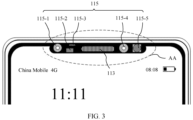
- a TOF or structured light 3D sensing module may be disposed on the top of the mobile phone 100, for example, at a "notch" location (namely, a region AA shown in FIG. 2 ) of the mobile phone 100.
- a structured light 3D sensing module 115 is integrated into the mobile phone 100.
- the structured light 3D sensing module 115 is arranged in the mobile phone 100 in the following form.
- the structured light 3D sensing module 115 includes modules such as an infrared camera 115-1, a flood illuminator 115-2, a short-distance sensor 115-3, an infrared image sensor 115-4, and a dot projector 115-5.
- a low-power laser for example, a VCSEL
- a lens including a component such as a diffuser are disposed in the flood illuminator 115-2.
- a high-power laser for example, a VCSEL
- a lens including a component such as a diffractive optical element are disposed in the dot projector 115-5.
- a process in which the structured light 3D sensing module 115 performs facial recognition is as follows: When an object (for example, a face) approaches the mobile phone 100, the short-distance sensor 115-3 senses that the object approaches the mobile phone 100, so that the short-distance sensor 115-3 sends, to the processor 101 of the mobile phone 100, a signal indicating that the object approaches.
- the processor 101 receives the signal indicating that the object approaches, and controls the flood illuminator 115-2 to be started, and the low-power laser in the flood illuminator 115-2 projects infrared laser light onto a surface of the object.
- the surface of the object reflects the infrared laser light projected by the flood illuminator 115-2, and the infrared camera 115-1 captures the infrared laser light reflected by the surface of the object, to obtain image information of the surface of the object, and then uploads the obtained image information to the processor 101.
- the processor 101 determines, based on the uploaded image information, whether the object approaching the mobile phone 100 is the face.
- the processor 101 controls the dot projector 115-5 to be started.
- the high-power laser in the dot projector 115-5 emits infrared laser light, and an element such as the diffractive optical element in the dot projector 115-5 performs an operation on the infrared laser light to form many (for example, approximately 30,000) structured light spots, and projects the structured light spots onto a surface of the face.
- An array formed by the structured light spots is reflected by different locations on the surface of the face.
- the infrared camera 115-1 captures the structured light spots reflected by the surface of the face, to obtain depth information of the different locations on the surface of the face, and then uploads the obtained depth information to the processor 101.
- the processor 101 compares and calculates the uploaded depth information and user's facial feature data that is pre-stored in the mobile phone 100, and identifies whether the face approaching the mobile phone 100 is the face of the user of the mobile phone 100, and if the face approaching the mobile phone 100 is the face of the user of the mobile phone 100, the processor 101 controls the mobile phone 100 to be unlocked; or if the face approaching the mobile phone 100 is not the face of the user of the mobile phone 100, the processor 101 controls the mobile phone 100 to remain in a locked state.
- the TOF or structured light 3D sensing module includes a module that can emit laser light, for example, a module that is in the TOF 3D sensing module and that includes a high-power laser, or the dot projector 115-5 and the flood illuminator 115-2 that are in the structured light 3D sensing module 115.
- This type of module is referred to as an active light emitting module below.
- FIG. 4a shows a typical structure of an active light emitting module 1.
- the active light emitting module 1 mainly includes a lens 11, a bottom substrate 17, a laser 18, and a microprocessor (MCU, Microcontroller Unit) 19.
- the lens 11 includes a lens tube 12, a lens component 13, and an optical element 14.
- the lens tube 12 is mounted on one side of the bottom substrate 17, and forms a receptacle BB with the bottom substrate 17.
- a holding structure 15 is disposed at an end that is inside the lens tube 12 and that is away from the bottom substrate 17.
- the holding structure 15 is a ring structure, and is disposed on an inner surface of the lens tube 12, to form a clear aperture GG.
- the laser 18, the microprocessor 19, the lens component 13, and the optical element 14 are all mounted in the receptacle BB.
- the laser 18 and the microprocessor 19 are mounted on the bottom substrate 17.
- the lens component 13 is mounted between the holding structure 15 and the bottom substrate 17.
- An edge of the optical element 14 is fastened, by using an adhesive 16, to a surface that is of the holding structure 15 and that is opposite to the laser 18.
- a microstructure layer 14-1 is disposed on a surface that is of the optical element 14 and that faces the laser 18, and the microstructure layer 14-1 includes a microstructure such as a diffraction grating or a dot, so that the optical element 14 has a specific function.
- a type of the laser 18 may be specifically a VCSEL, a DFB (Distributed Feedback Laser, distributed feedback laser), an edge-emitting laser, or the like.
- the lens component 13 includes at least one optical lens. When the lens component 13 includes a plurality of optical lenses, the lens component 13 is formed by superimposing the plurality of optical lenses.
- the optical lens may be, for example, a convex lens.
- the lens component 13 is configured to collimate and converge laser light emitted by the laser 18.
- a type of the optical element 14 may be specifically a diffuser, a diffractive optical element, a Fresnel lens, or the like.
- the optical element 14 may be specifically a diffuser, and the microstructure layer 14-1 of the optical element 14 includes a diffusion microstructure such as the dot.
- the optical element 14 may be specifically a diffractive optical element (DOE), and the microstructure layer 14-1 of the optical element 14 includes a diffraction grating microstructure.
- DOE diffractive optical element
- the active light emitting module 1 may be mounted in a terminal such as the mobile phone 100, a side of the laser 18 (namely, a light emitting side) in the active light emitting module 1 is close to inside of the terminal, and a side of the optical element 14 (namely, a light output side) faces outside of the terminal, to project laser light outward.
- the microprocessor 19 is connected to a processor integrated on a mainboard of the terminal. For example, if the active light emitting module 1 is applied to the mobile phone 100, the microprocessor 19 of the active light emitting module 1 is connected to the processor 101 of the mobile phone 100.
- the microprocessor 19 is connected to the laser 18, and controls the laser 18 to transmit laser light.
- the laser light passes through the lens component 13, passes through the clear aperture GG, and then is emitted out of the active light emitting module 1 through the optical element 14.
- the optical element 14 in the active light emitting module 1 may be damaged or fall off due to water penetration, erosion, or the like.
- the laser light emitted by the laser 18 in the active light emitting module 1 leak out and is directed onto a human eye. Consequently, the human eye may be damaged. If the laser 18 in the active light emitting module 1 emits high-power laser light, damage to the human eye is more serious.
- a damage or fall-off status of the optical element 14 in the active light emitting module 1 needs to be monitored, so that when the optical element 14 is damaged or falls off, a response measure such as turning off the laser 18 is taken in a timely manner, to avoid leakage of the laser light emitted by the laser 18.
- a conductive layer is disposed on a surface of the optical element 14 to monitor the damage or fall-off status of the optical element 14. For details, refer to FIG. 5a to FIG. 5c .
- a conductive layer 20 is disposed on the surface that is of the optical element 14 and that is opposite to the laser 18. According to the invention, the conductive layer 20 includes a detection line 20-1.
- a material of the detection line 20-1 is a transparent conductive material such as ITO (indium tin oxide), IZO (indium zinc oxide), IGZO (indium gallium zinc oxide), or ITZO (indium tin zinc oxide).
- ITO indium tin oxide
- IZO indium zinc oxide
- IGZO indium gallium zinc oxide
- ITZO indium tin zinc oxide
- the conductive layer 20 further includes conductive pads 20-2 that are respectively disposed on the two ends of the detection line 20-1.
- a conductive electrode 22 is disposed above the conductive pad 20-2 and an end that is of the conducting wire 21 and that is connected to the detection line 20-1, so that the detection line 20-1 is electrically connected to the conducting wire 21 through the conductive pad 20-2 and the conductive electrode 22.
- the microprocessor 19 provides a voltage for an entire monitoring circuit, and monitors a resistance value of the detection line 20-1 or a voltage value at two ends of the detection line 20-1 in real time.
- the resistance value of the detection line 20-1 or the voltage value at both ends of the detection line 20-1 changes abnormally, for example, the resistance value of the detection line 20-1 exceeds a set resistance threshold range, or the voltage value at both ends of the detection line 20-1 exceeds a set voltage threshold range, it indicates that the monitoring circuit is open-circuited.
- the detection line 20-1 may be broken, or an open circuit may occur at a joint between the detection line 20-1 and the conducting wire 21.
- a reason why the detection line 20-1 is broken may be that the optical element 14 to which the detection line 20-1 is attached is damaged, and a reason why the open circuit occurs at the joint between the detection line 20-1 and the conducting wire 21 may be that the optical element 14 to which the detection line 20-1 is attached falls off. Therefore, when the microprocessor 19 detects that the resistance value of the detection line 20-1 exceeds the set resistance threshold range, or that the voltage value at both ends of the detection line 20-1 exceeds the set voltage threshold range, it may be determined that the optical element 14 is damaged or falls off.
- the microprocessor 19 controls a power supply 2 to stop supplying power to the laser 18, and the laser 18 is turned off, thereby effectively preventing the laser light emitted by the laser 18 from leaking out and being directly onto the human eye, so that the damage to the human eye is avoided.
- the detection line 20-1 is broken, or the joint between the detection line 20-1 and the conducting wire 21 is disconnected. Therefore, in this case, the resistance value that is of the detection line 20-1 and that is monitored by the microprocessor 19 becomes very large or even infinite ( ⁇ ), or the voltage value at the two ends of the detection line 20-1 is close to or equal to a voltage value provided by the microprocessor 19 for the entire monitoring circuit.
- the "set resistance threshold range” mentioned above may be set to a numerical range that fluctuates around a resistance value R obtained when the detection line 20-1 is not broken.
- the “set resistance threshold range” may be set to be greater than or equal to 80%R and less than or equal to 120%R.
- the “set resistance threshold range” may be set to be greater than or equal to 8 K ⁇ and less than or equal to 12 K ⁇ .
- the "set voltage threshold range” mentioned above may be set to a numerical range that fluctuates around a voltage value U that is shared by the detection line 20-1 in the entire monitoring circuit and that is obtained when the detection line 20-1 is not broken.
- the “set voltage threshold range” may be set to be greater than or equal to 80%U and less than or equal to 120%U.
- the “set voltage threshold range” may be set to be greater than or equal to 0.64 V and less than or equal to 0.96 V
- the conductive layer 20 needs to be disposed on the surface that is of the optical element 14 and that is opposite to the laser 18, that is, the conductive layer 20 is disposed on a surface that is of the optical element 14 and that faces outside of the module.
- the conductive layer 20 is disposed on the surface that is of the optical element 14 and that faces the outside of the module. Therefore, the static electricity easily enters the conductive layer 20. A voltage of the static electricity is very high, and the conductive layer 20 is damaged.
- the detection line 20-1 in the conductive layer 20 is broken, and a monitoring function of the detection line 20-1 on the damage or fall-off status of the optical element 14 fails.
- the static electricity entering the conductive layer 20 may be conducted to the microprocessor 19 along the conducting wire 21 connected to the conductive layer 20, to damage the microprocessor 19.
- the embodiments of the present invention provide a lens.
- the lens 11 is applied to the active light emitting module 1, and the lens 11 includes the lens tube 12 and the optical element 14.
- the lens tube 12 has a top surface 12a and a bottom surface (not shown in the figure) opposite to the top surface 12a.
- the bottom surface is connected to the bottom substrate 17 of the active light emitting module 1.
- the top surface 12a is located on a side that is of the lens tube 12 and that is away from the bottom substrate 17.
- the top surface 12a is a frame-shaped surface.
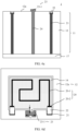
- the holding structure 15 is disposed on a side on which the top surface 12a is located in the lens tube 12. Referring to FIG. 4b , the holding structure 15 is a ring structure, and is disposed on the inner surface of the lens tube 12, to form the clear aperture GG.
- the optical element 14 is mounted in the lens tube 12 and is located on a side on which the top surface 12a of the lens tube 12 is located.
- the edge of the optical element 14 is fastened, by using the adhesive 16, to a surface that is of the holding structure 15 and that faces a side on which the top surface 12a of the lens tube 12 is located.
- the conductive layer 20 configured to monitor the damage or fall-off status of the optical element 14 is disposed on a surface that is of the optical element 14 and that faces the side on which the top surface 12a of the lens tube 12 is located.
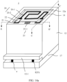
- the lens 11 further includes an antistatic structure 23 disposed on the top surface 12a of the lens tube 12, and an electrostatic conducting wire 24 disposed inside a tube wall or on an inner surface or an outer surface of the lens tube 12.
- the antistatic structure 23 and the electrostatic conducting wire 24 are both electrically conductive, and the two are electrically connected.
- one end that is of the electrostatic conducting wire 24 and that is away from the antistatic structure 23 is grounded. For example, as shown in FIG.
- a ground terminal 25 is disposed on the bottom substrate 17 of the active light emitting module 1, and the end that is of the electrostatic conducting wire 24 and that is away from the antistatic structure 23 may be connected to the ground terminal 25, so that the antistatic structure 23 and the electrostatic conducting wire 24 are grounded.
- the antistatic structure 23 can guide static electricity passing through the antistatic structure 23 to the ground terminal through the electrostatic conducting wire 24, and the antistatic structure 23 can further attract static electricity near the antistatic structure 23, and then guide the attracted static electricity to the ground terminal through the electrostatic conducting wire 24.
- the antistatic structure 23 is located in at least a part of an area around the conductive layer 20, so that the antistatic structure 23 can guide at least a part of static electricity close to the conductive layer 20 to the ground terminal 25, reducing an amount of static electricity entering the conductive layer 20, effectively reducing a risk that the conductive layer 20 is damaged by the static electricity, and therefore protecting the conductive layer 20. Further, because the antistatic structure 23 reduces the amount of static electricity entering the conductive layer 20, a risk that the static electricity enters the microprocessor 19 along the conducting wire 21 connected to the conductive layer 20 and damages the microprocessor 19 is also reduced.
- the antistatic structure 23 includes at least one antistatic electrode 23-1.
- the antistatic structure 23 includes one antistatic electrode 23-1.
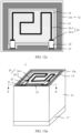
- An orthographic projection of the antistatic electrode 23-1 on a plane defined by the optical element 14 is located in a surrounding area of the optical element 14 in which the conductive layer 20 is located, so that static electricity passing through the antistatic electrode 23-1 and around the antistatic electrode 23-1 can be guided to the ground terminal 25.
- the antistatic structure 23 includes a plurality of antistatic electrodes 23-1, and the plurality of antistatic electrodes 23-1 are electrically connected to each other through a first electrode connection wire 23-2, so that the plurality of antistatic electrodes 23-1 may be grounded through one electrostatic conducting wire 24.
- the plurality of antistatic electrodes 23-1 are disposed at intervals on the top surface 12a of the lens tube 12. Further, the plurality of antistatic electrodes 23-1 are disposed at equal intervals around the optical element 14 in which the conductive layer 20 is located, so that an antistatic capability of the antistatic structure 23 to guide static electricity in all areas around the conductive layer 20 can be improved.
- electrical connection may not be performed between the plurality of antistatic electrodes 23-1, and each antistatic electrode 23-1 is independently grounded through the electrostatic conducting wire 24.
- one antistatic electrode 23-1 may be disposed on one side of each side of the optical element 14.
- the antistatic electrode 23-1 may be in a square shape, for example, in a rectangle shape.
- two antistatic electrodes 23-1 may be disposed on one side of each long side of the optical element 14, and one antistatic electrode 23-1 may be disposed on one side of each short side of the optical element 14.
- the antistatic electrode 23-1 may be in a square shape, for example, in a rectangle shape.
- one antistatic electrode 23-1 may be disposed in each of four corners of the optical element 14.
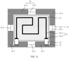
- the antistatic electrode 23-1 may be in an L shape. It can be imagined that the plurality of antistatic electrodes 23-1 may further be disposed in other manners. These are not listed one by one herein.
- a smaller spacing d between the orthographic projection of the antistatic electrode 23-1 on the plane defined by the optical element 14 and the optical element 14 is preferred.
- an antistatic capability of the antistatic electrode 23-1 to protect the conductive layer 20 attached to the optical element 14 can be improved as much as possible.
- an edge that is of the orthographic projection of the antistatic electrode 23-1 on the plane defined by the optical element 14 and that is close to the optical element 14 coincides with a corresponding inner side edge of the top surface 12a, to minimize, as much as possible, the spacing d between the orthographic projection of the antistatic electrode 23-1 on the plane defined by the optical element 14 and the optical element 14.
- a length L of the antistatic electrode 23-1 may be set to any value. This is not limited in the embodiments of the present invention.
- the length L of the antistatic electrode 23-1 is less than or equal to a length of a side of the optical element 14 corresponding to the antistatic electrode 23-1.
- a shape of the antistatic electrode 23-1 may be set to any shape. This is not limited in the embodiments of the present invention.
- the shape of the antistatic electrode 23-1 is a rectangle (as shown in FIG. 6d , FIG. 7a , and FIG. 7b ), or the shape of the antistatic electrode 23-1 is an L shape (as shown in FIG. 7c ).
- shapes and sizes of the plurality of antistatic electrodes 23-1 may be the same, to simplify process steps of manufacturing the plurality of antistatic electrodes 23-1.
- the antistatic structure 23 is a frame-shaped conductive film, and extends along the frame-shaped top surface 12a of the lens tube 12, so that the antistatic structure 23 completely surrounds the conductive layer 20 within an area framed by the antistatic structure 23, and can guide static electricity from all areas around the conductive layer 20 to the ground terminal 25, greatly improving an antistatic effect of the antistatic structure 23 on the conductive layer 20.
- widths of all parts of the frame-shaped conductive film used as the antistatic structure 23 are equal or unequal.
- Two ends of the detection line 20-1 of the conductive layer 20 are respectively connected to two conducting wires 21.
- the antistatic structure 23 avoids, at a position at an end (which is specifically referred to an end that is of the conducting wire 21 and that is connected to the detection line 20-1, and the end is referred to as a detection line connecting end below) of the conducting wire 21, the detection line connecting end of the conducting wire 21, so as to avoid an electrical connection to the detection line connecting end of the conducting wire 21.
- widths of parts except the position of the corresponding detection line connecting end of the conducting wire 21 are equal.
- a spacing d' between each other position and the optical element 14 is equal.
- the antistatic capabilities of parts except the position of the corresponding detection line connecting end of the conducting wire 21 are uniform and consistent.
- a smaller spacing d' is preferred. In this way, an antistatic capability of the antistatic structure 23 to protect the conductive layer 20 attached to the optical element 14 can be improved as much as possible.
- an edge that is of the remaining part and that is close to the optical element 14 coincides with a corresponding inner side edge of the top surface 12a, to reduce the spacing d' as much as possible.
- a fracture Q may be disposed on the frame-shaped conductive film of the antistatic structure 23.
- the fracture Q may be disposed at any position except a position that is of the antistatic structure 23 and that is electrically connected to the electrostatic conducting wire 24. In this way, both a conductive film from one side of the fracture Q to the position that is of the antistatic structure 23 and that is electrically connected to the electrostatic conducting wire 24 and a conductive film from the other side of the fracture Q to the position that is of the antistatic structure 23 and that is electrically connected to the electrostatic conducting wire 24 can be grounded through the electrostatic conducting wire 24.
- the fracture Q may be disposed on a side of any side of the optical element 14, provided that the fracture Q is away from the position that is of the antistatic structure 23 and that is electrically connected to the electrostatic conducting wire 24.
- the optical element 14 includes a first side and a second side that are opposite to each other. The position that is of the antistatic structure 23 and that is electrically connected to the electrostatic conducting wire 24 is located on a side of the first side of the optical element, and the fracture Q is disposed on a side of the second side of the optical element.
- the position that is of the antistatic structure 23 and that is electrically connected to the electrostatic conducting wire 24 is located on a side of a midpoint position of the first side of the optical element, and the fracture Q is disposed on a side of a midpoint position of the second side of the optical element.
- the conductive film from one side of the fracture Q to the position that is of the antistatic structure 23 and that is electrically connected to the electrostatic conducting wire 24 and the conductive film from the other side of the fracture Q to the position that is of the antistatic structure 23 and that is electrically connected to the electrostatic conducting wire 24 have an equal or approximately equal length. This helps improve the antistatic capability of the antistatic structure 23.
- a material of the antistatic structure 23 may be a material with a relatively low resistivity.
- the material of the antistatic structure 23 may be a material with a resistivity less than the resistivity of the conductive layer 20, so as to effectively attract and guide static electricity that is to enter the conductive layer 20.
- a metal material such as copper (Cu), chromium (Cr), or silver (Ag) may be used as the material of the antistatic structure 23.
- a material of the antistatic electrode 23-1 may be selected according to the foregoing principle.
- a material of the first electrode connection wire 23-2 may be the same as the material of the antistatic electrode 23-1. In this way, the antistatic electrode 23-1 and the first electrode connection wire 23-2 may be manufactured in a same step, thereby simplifying process steps.
- a material of the lens tube 12 is LDS (Laser Direct structuring, laser direct structuring) plastic.
- the LDS plastic is a modified plastic that includes an organic metal complex. After being irradiated by a laser, the organic metal complex in the LDS plastic can release metal particles, so that a laser irradiated area becomes electrically conductive.
- the antistatic structure 23 may be manufactured by using an LDS technology.
- a manufacturing process is generally as follows: An area of the antistatic structure 23 to be formed on the top surface 12a of the lens tube 12 is irradiated by using a laser, so that metal particles are released from an organic metal complex in the laser irradiated area, and the LDS plastic material in the laser irradiated area is activated and becomes conductive, to form a pattern of the antistatic structure 23.
- a process of manufacturing the antistatic structure 23 by using the LDS technology is simple, and no additional conductive material needs to be prepared for forming the antistatic structure 23.
- the antistatic structure 23 may be manufactured by using any one of processes such as electroplating, screen printing, coating, magnetron sputtering, and photolithography. This is not limited in the present invention.
- a formed antistatic structure 23 may be directly fastened to the top surface 12a of the lens tube 12 by pasting, welding, or the like.
- the antistatic structure 23 and the electrostatic conducting wire 24 may be connected by welding, to ensure that the antistatic structure 23 is electrically connected to the electrostatic conducting wire 24.
- a protective layer may be covered on the antistatic structure 23, to prevent the antistatic structure 23 from being corroded by factors such as water vapor and oxygen in an external environment, and protect the antistatic structure 23.
- a material of the protective layer may be an organic or inorganic material that has water and oxygen isolation and erosion resistance performance.
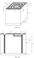
- the electrostatic conducting wire 24 extends inside the tube wall of the lens tube 12.
- One end of the electrostatic conducting wire 24 extends to the antistatic structure 23, and the other end extends to the ground terminal 25 of the bottom substrate 17.
- the electrostatic conducting wire 24 is disposed inside the tube wall of the lens tube 12, so that the electrostatic conducting wire 24 can be prevented from being corroded by the factors such as water vapor and oxygen in the external environment while implementing grounding of the antistatic structure 23, to protect the electrostatic conducting wire 24.
- an insert molding (Insert Molding) technology may be used to integrally mold the electrostatic conducting wire 24 and the lens tube 12.
- a channel may be formed in the lens tube 12, and then a solution of the material of the electrostatic conducting wire 24 is injected into the channel, to form the electrostatic conducting wire 24.
- the electrostatic conducting wire 24 extends on an outer surface of the lens tube 12.
- the electrostatic conducting wire 24 extends on an inner surface of the lens tube 12.
- the electrostatic conducting wire 24 may be formed on the outer surface or the inner surface of the lens tube 12 through coating, printing, pasting, or the like.
- a protective layer may be formed on the electrostatic conducting wire 24 to cover the electrostatic conducting wire 24, to prevent the electrostatic conducting wire 24 from being exposed and being corroded.
- a material of the protective layer may be an organic or inorganic material that has water and oxygen isolation and erosion resistance performance.
- a material of the electrostatic conducting wire 24 may be a material having conductive performance, for example, a metal conductive material such as silver (Ag), copper (Cu), or chromium (Cr), a semiconductor conductive material, or an oxide conductive material. Further, the material of the electrostatic conducting wire 24 may be the same as a material of the antistatic structure 23, to reduce contact resistance between the electrostatic conducting wire 24 and the antistatic structure 23.
- a metal conductive material such as silver (Ag), copper (Cu), or chromium (Cr)
- the material of the electrostatic conducting wire 24 may be the same as a material of the antistatic structure 23, to reduce contact resistance between the electrostatic conducting wire 24 and the antistatic structure 23.
- two ends of the detection line 20-1 of the conductive layer 20 are respectively connected, through two conducting wires 21, to the microprocessor 19 disposed on the bottom substrate 17 of the active light emitting module 1.
- the two conducting wires 21 extend in the lens tube 12, or on an inner surface or an outer surface of the lens tube 12. Referring to FIG. 5a , a manner in which the two conducting wires 21 are connected to the microprocessor 19 is as follows: A positive terminal e and a negative terminal f are disposed on the bottom substrate 17 of the active light emitting module 1, the two conducting wires 21 are respectively connected to the positive terminal e and the negative terminal f, and the positive terminal e and the negative terminal f are respectively connected to two ports of the microprocessor 19.
- the negative terminal f is connected to the ground terminal 25 disposed on the bottom substrate 17, or the negative terminal and the ground terminal 25 are configured as a same terminal. In this way, it is equivalent to that the conducting wire 21 that is in the two conducting wires 21 and that is connected to the negative terminal f is grounded. Because one end that is of the electrostatic conducting wire 24 connected to the antistatic structure 23 and that is away from the antistatic structure 23 needs to be grounded, and the electrostatic conducting wire 24 extends in the lens tube 12, or on the inner surface or the outer surface of the lens tube 12, as shown in FIG. 10a to FIG. 10c , FIG. 11a to FIG. 11c , FIG. 12a to FIG. 12c , and FIG. 13a to FIG.
- the electrostatic conducting wire 24 may reuse the conducting wire 21 (the conducting wire 21 is referred to as a negative electrode ground wire below) that is connected to the negative terminal f and that is grounded in the two conducting wires 21. That is, the electrostatic conducting wire 24 and the negative electrode ground wire are configured as a same conductive line. In this way, a structure and a manufacturing process of the lens 11 can be simplified.
- the electrostatic conducting wire 24 and the negative electrode ground wire are configured as a same conductive line, because the negative electrode ground wire (namely, the electrostatic conducting wire 24) is grounded, static electricity transmitted to the negative electrode ground wire (namely, the electrostatic conducting wire 24) through the antistatic structure 23 is preferably transmitted (flowing) to the ground terminal, and is not transmitted to the conductive layer 20 along the negative electrode ground wire (namely, the electrostatic conducting wire 24). In this way, it is ensured that an electrostatic protection effect of the antistatic structure 23 on the conductive layer 20 is achieved.
- the lens 11 further includes a second electrode connection wire 26.
- the second electrode connection wire 26 electrically connects the antistatic structure 23 and the negative electrode ground wire, so that the negative electrode ground wire is used as the electrostatic conducting wire 24.
- the antistatic structure 23 is grounded through the second electrode connection wire 26 and the negative electrode ground wire (namely, the electrostatic conducting wire 24).
- the antistatic structure 23 includes one antistatic electrode 23-1.
- the antistatic electrode 23-1 may be disposed between ends that are of the two conducting wires 21 and that are connected to the detection line 20-1 (that is, between the two conductive electrodes 22). In this way, a distance between the antistatic electrode 23-1 and the negative electrode ground wire is relatively short. This helps shorten a length of the second electrode connection wire 26.
- the antistatic structure 23 includes a plurality of antistatic electrodes 23-1
- the plurality of antistatic electrodes 23-1 are connected to each other through the first electrode connection wire 23-2
- an antistatic electrode 23-1 that is in the plurality of antistatic electrodes 23-1 and that is closest to the negative electrode ground wire is connected to the negative electrode ground wire through the second electrode connection wire 26.
- the antistatic electrode 23-1 that is in the plurality of antistatic electrodes 23-1 and that is closest to the negative electrode ground wire is disposed between the ends that are of the two conducting wires 21 and that are connected to the detection line 20-1 (that is, between the two conductive electrodes 22).
- FIG. 12a to FIG. 12c for a lens 11 in which the antistatic structure 23 is a frame-shaped conductive film.
- a joint of the antistatic structure 23 and the second electrode connection wire 26 may be disposed between ends that are of the two conducting wires 21 and that are connected to the detection line 20-1 (that is, between the two conductive electrodes 22). In this way, a distance between the negative electrode ground wire and the joint of the antistatic structure 23 and the second electrode connection wire 26 is relatively short. This helps shorten a length of the second electrode connection wire 26.
- the second electrode connection wire 26 may be disposed inside the tube wall, or on the outer surface or the inner surface of the lens tube 12. This is not limited in the embodiments of the present invention.
- the second electrode connection wire 26 and the negative electrode ground wire (namely, the electrostatic conducting wire 24) may be disposed in a same manner.
- both the second electrode connection wire 26 and the negative electrode ground wire (namely, the electrostatic conducting wire 24) are disposed inside the tube wall of the lens tube 12, or both are disposed on the outer surface of the lens tube 12, or both are disposed on the inner surface of the lens tube.
- FIG. 10a to FIG. 10c , and FIG. 12a to FIG. 12c show examples in which both are disposed inside the tube wall of the lens 12.
- the second electrode connection wire 26 and the negative electrode ground wire (namely, the electrostatic conducting wire 24) may be formed in a same step. This helps simplify the manufacturing process of the lens 11.
- a material of the second electrode connection wire 26 may be a material having conductive performance, for example, a metal conductive material such as silver (Ag), copper (Cu), or chromium (Cr), a semiconductor conductive material, or an oxide conductive material. Further, the material of the second electrode connection wire 26 may be the same as that of the negative electrode ground wire (namely, the electrostatic conducting wire 24), so that the second electrode connection wire 26 and the negative electrode ground wire (namely, the electrostatic conducting wire 24) may be formed in a same step.
- a metal conductive material such as silver (Ag), copper (Cu), or chromium (Cr)
- the material of the second electrode connection wire 26 may be the same as that of the negative electrode ground wire (namely, the electrostatic conducting wire 24), so that the second electrode connection wire 26 and the negative electrode ground wire (namely, the electrostatic conducting wire 24) may be formed in a same step.
- the electrostatic conducting wire 24 and the negative electrode ground wire are configured as a same conductive line, for example, in FIG. 11a to FIG. 11c and FIG. 13a to FIG. 13c , a part of an end that is close to the negative electrode ground wire and that is connected to the detection wire 20-1 in the antistatic structure 23 extends to an end that is of the negative electrode ground wire and that is connected to the detection wire 20-1, so that the antistatic structure 23 is electrically connected to the negative electrode ground wire, the negative electrode ground wire is used as the electrostatic conducting wire 24, and the antistatic structure 23 is grounded through the negative electrode ground wire (namely, an electrostatic conducting wire 24).
- the antistatic structure 23 includes one antistatic electrode 23-1.
- the antistatic electrode 23-1 may be disposed between ends that are of the two conducting wires 21 and that are connected to the detection line 20-1 (that is, between the two conductive electrodes 22).
- the part of the end that is close to the negative electrode ground wire and that is connected to the detection wire 20-1 in the antistatic structure 23 extends to the end that is of the negative electrode ground wire and that is connected to the detection wire 20-1.
- the antistatic electrode 23-1 can be electrically connected to the negative electrode ground wire without an additional structure used to electrically connect the antistatic electrode 23-1 and the negative electrode ground wire.
- the structure is simple and easy to implement.
- the antistatic structure 23 includes a plurality of antistatic electrodes 23-1
- the plurality of antistatic electrodes 23-1 are connected to each other through the first electrode connection wire 23-2, and an antistatic electrode 23-1 that is in the plurality of antistatic electrodes 23-1 and that is closest to the negative electrode ground wire is extended to an end that is of the negative electrode ground wire and that is connected to the detection line 20-1, so that the plurality of antistatic electrodes 23-1 are electrically connected to the negative electrode ground wire.
- the antistatic electrode 23-1 that is in the plurality of antistatic electrodes 23-1 and that is closest to the negative electrode ground wire is disposed between the ends that are of the two conducting wires 21 and that are connected to the detection line 20-1 (that is, between the two conductive electrodes 22).
- the antistatic electrode 23-1 is electrically connected to the negative electrode ground wire, refer to FIG. 11b and FIG. 11c .
- FIG. 13a to FIG. 13c for a lens 11 in which the antistatic structure 23 is a frame-shaped conductive film.
- a part of an end that is close to the negative electrode ground wire and that is connected to the detection wire 20-1 in the antistatic structure 23 may be extended to an end that is of the negative electrode ground wire and that is connected to the detection line 20-1, so that the antistatic structure 23 is electrically connected to the negative electrode ground wire.
- the lens 11 further includes the lens component 13.
- the lens component 13 is mounted inside the lens tube 12, and is located on a side that is of the holding structure 15 and that is opposite to the optical element 14.
- the lens component 13 may be fastened inside the lens tube 12 through bonding, clamping, embedding, or the like.
- the lens component 13 includes at least one optical lens.
- the lens component 13 is formed by superimposing the plurality of optical lenses.
- the optical lens may be, for example, a convex lens.
- the lens component 13 is configured to collimate and converge light passing through the lens component 13.
- the embodiments of the present invention further provide an active light emitting module.
- the active light emitting module 1 includes at least the lens 11, the bottom substrate 17, the laser 18, and the microprocessor 19 that are provided in the embodiments of the present invention.
- the lens 11 includes the lens tube 12, the lens component 13, and the optical element 14.
- the lens tube 12 is mounted on one side of the bottom substrate 17, and forms a receptacle BB with the bottom substrate 17.
- the laser 18, the microprocessor 19, the lens component 13, and the optical element 14 are all mounted in the receptacle BB.
- the conductive layer 20 configured to monitor the damage or fall-off status of the optical element 14 is disposed on the surface that is of the optical element 14 and that is opposite to the laser 18.
- the antistatic structure 23 is disposed on the top surface 12a of the lens tube 12.
- the electrostatic conducting wire 24 is disposed inside the tube wall, or on the inner surface or the outer surface of the lens tube 12.
- the ground terminal 25 is disposed on the bottom substrate 17.
- One end of the electrostatic conducting wire 24 is connected to the antistatic structure 23, and the other end is connected to the ground terminal 25, so that the antistatic structure 23 is grounded.
- the antistatic structure 23 can guide static electricity passing through the antistatic structure 23 to the ground terminal through the electrostatic conducting wire 24, and the antistatic structure 23 can further attract static electricity near the antistatic structure 23, and then guide the attracted static electricity to the ground terminal through the electrostatic conducting wire 24. This effectively reduces a risk that the conductive layer 20 is damaged by the static electricity, and protects the conductive layer 20 and the microprocessor 19 connected to the conductive layer 20.
- the ground terminal 25 may be disposed in the receptacle BB. In this way, an end that is of the electrostatic conducting wire 24 and that is connected to the ground terminal 25 needs to extend to inside of the receptacle BB, and is electrically connected to the ground terminal 25.
- the ground terminal 25 may further be disposed outside the receptacle BB. In this way, the end that is of the electrostatic conducting wire 24 and that is connected to the ground terminal 25 needs to extend to the inside of the receptacle BB, and is electrically connected to the ground terminal 25.
- two ends of the detection line 20-1 of the conductive layer 20 of the optical element 14 are separately connected, through two conducting wires 21, to the microprocessor 19 disposed on the bottom substrate 17 of the active light emitting module 1.
- a manner in which the two conducting wires 21 are connected to the microprocessor 19 is as follows: The positive terminal e and the negative terminal f are disposed on the bottom substrate 17, the two conducting wires 21 are respectively connected to the positive terminal e and the negative terminal f, and the positive terminal e and the negative terminal f are respectively connected to two ports of the microprocessor 19.
- the negative terminal and the ground terminal 25 are configured as a same terminal.
- the conducting wire 21 (namely, the negative electrode ground wire) that is in the two conducting wires 21 and that is connected to the negative terminal f is grounded.
- the electrostatic conducting wire 24 connected to the antistatic structure 23 and the negative electrode ground wire are configured as a same conductive line, and the antistatic structure 23 and the negative electrode ground wire (namely, the electrostatic conducting wire 24) are electrically connected.
- the positive terminal e and the negative terminal f are disposed outside the receptacle BB, and ends that are of the two conducting wires 21 and that are connected to the positive terminal e and the negative terminal f (namely, the ground terminal 25) extend to outside of the receptacle BB to connect to a corresponding electrical terminal (namely, the positive terminal e or the negative terminal f).
- a protruding part 12-1 is disposed on an outer surface of the lens tube 12, and the protruding part 12-1 is located at least above the positive terminal e and the negative terminal f.
- the ends that are of the two conducting wires 21, which are the positive terminal e and the negative terminal f, may extend to the protruding part 12-1, so as to extend to an upper part of the positive terminal e and the negative terminal f, and be connected to the corresponding electrical terminal.
- the positive terminal e and the negative terminal f may alternatively be disposed inside the receptacle BB, and the ends that are of the two conducting wires 21 and that are connected to the positive terminal e and the negative terminal f (namely, the ground terminal 25) extend to inside of the receptacle BB to connect to the corresponding electrical terminal (namely, the positive terminal e or the negative terminal f).
- the active light emitting module 1 is any module that can emit laser light, for example, the module that is in the TOF 3D sensing module and that includes the high-power laser, or the dot projector 115-5 and the flood illuminator 115-2 that are in the structured light 3D sensing module 115.
- an embodiment of the present invention further provides a terminal.
- the terminal includes the active light emitting module 1 provided in the embodiments of the present invention, configured to provide specified laser light (for example, if the active light emitting module 1 is the dot projector 115-5, the specified light that needs to be provided by the active light emitting module 1 is structured light), to assist the terminal in implementing a 3D sensing function.
- the active light emitting module 1 is mounted in a terminal such as the mobile phone 100, a side of the laser 18 (namely, a light emitting side) in the active light emitting module 1 is close to inside of the terminal, and a side of the optical element 14 (namely, a light output side) faces outside of the terminal, to project the specified laser light outward.
- a side of the laser 18 namely, a light emitting side
- a side of the optical element 14 namely, a light output side
Landscapes
- Engineering & Computer Science (AREA)
- Theoretical Computer Science (AREA)
- Physics & Mathematics (AREA)
- General Engineering & Computer Science (AREA)
- General Physics & Mathematics (AREA)
- Signal Processing (AREA)
- Human Computer Interaction (AREA)
- Computer Hardware Design (AREA)
- Computer Security & Cryptography (AREA)
- Optics & Photonics (AREA)
- Electromagnetism (AREA)
- Radar, Positioning & Navigation (AREA)
- Remote Sensing (AREA)
- Computer Networks & Wireless Communication (AREA)
- Software Systems (AREA)
- Telephone Function (AREA)
- Studio Devices (AREA)
Description
- The present invention relates to the field of electronic terminal device technologies, and in particular, to a lens, an active light emitting module, and a terminal.
- Currently, a 3D sensing technology is a hot research topic in an electronic terminal device (for example, a mobile phone) field. The 3D sensing technology is a deep sensing technology that can further improve a facial recognition or iris recognition function and enhance a facial and object recognition function of a terminal camera, and is applicable to functions such as augmented reality, a game, and self-driving.
- Active light emitting modules such as structured light and a ToF (Time Of Flight, time of flight) are integrated into a terminal, so that a 3D sensing function can be implemented. This type of active light emitting module usually includes a laser and a lens disposed in a light emitting direction of the laser. The laser can emit laser light, and the lens includes an optical element such as a diffractive optical element (Diffractive Optical Element, DOE for short) or a diffuser (Diffuser) that is configured to disperse light or diffuse light. If the optical element such as the diffractive optical element or the diffuser in the lens is damaged or falls off, the laser light emitted by the laser may leak out, and direct exposure of the laser light to human eyes may damage human eye vision. Therefore, a damage or fall-off status of the optical element such as the diffractive optical element or the diffuser needs to be monitored.
- By disposing a conductive layer on a surface of the optical element, a change of an electrical signal on the conductive layer is monitored in real time, so that the damage or fall-off status of the optical element can be monitored. However, in processes such as production of an optical element, assembly of an active light emitting module, and use of a terminal, static electricity is generated. The static electricity enters the conductive layer, and damages the conductive layer. Consequently, a monitoring function of the conductive layer fails.
CN 108 594 563 A discloses a structured light projective module, an image capturing apparatus and electronic equipment. The structured light projective module comprises a laser transmitter, an optical assembly and a circuit board assembly; the laser transmitter is used for transmitting laser; the optical assembly is arranged on the light emitting optical path of the laser transmitter, and the laser passes through the optical assembly to form a laser pattern; the optical assembly is provided with a detection element which is used for outputting an electric signal for detecting whether the optical assembly is cracked or not; the circuit board assembly comprises a first connecting board, a bent board and a second connecting board which are connected in sequence; the detection element is connected with the first connecting board through the second connecting board and the bent board; and the laser transmitter is arranged on the first connecting board. By virtue of the embodiments of the structured light projective module, the image capturing apparatus and the electronic equipment, electrical connection of the detection element and a processor can be realized through the bendable circuit board, so that the processor can judge whether the optical assembly is cracked or not according to the electric signal output by the detection element, thereby improving the use safety of the structured light projective module.
CN 107 870 186 A discloses an optical module with a safety monitoring function. The optical module comprises an optical component, a transparent substrate and a control circuit, wherein a transparent conductive thin film is attached to the transparent substrate; the transparent substrate is fixedly arranged outside the optical component through a support piece, and is used for protecting the optical component; the control circuit is electrically connected with the transparent conductive thin film, and is used for monitoring a change of the transparent conductive thin film and evaluating the integrity of the transparent substrate to further judge the integrity of the optical component. According to the optical module, the transparent substrate is arranged outside the optical component, and thetransparent conductive thin film is attached to the surface of the transparent substrate to monitor the change of the transparent conductive thin film in real time and indirectly evaluate and judge the integrity of the transparent substrate to further judge the integrity of the optical component, so that the safety monitoring function is realized.
KR 2005 0020516 A
US 2015/077654 A1 discloses a touch panel having a light transmitting area and a light shielding area adjacent to the light transmitting area. The touch panel includes a cover plate, a first decoration layer, a touch-sensing element and a metal conductive layer. The first decoration layer is disposed on the cover plate and located in the light shielding area. The first decoration layer has at least one hollow area. The touch-sensing element is disposed on the cover plate and at least located in the light transmitting area. The metal conductive layer is disposed on the first decoration layer, located in the light shielding area and surrounds the touch-sensing element. A portion of the metal conductive layer surrounds the hollow area. - The present invention provides a lens of
claim 1, an active light emitting module ofclaim 13, and a terminal ofclaim 15, to protect a conductive layer on an optical element and reduce a risk that the conductive layer is damaged by static electricity. - To achieve the foregoing objective, the following technical solutions are used in the present invention.
- According to a first aspect of the present invention, a lens is provided. The lens includes a lens tube and an optical element mounted in the lens tube. The lens tube has a top surface, and a conductive layer is disposed on a surface that is of the optical element and that faces a side on which the top surface is located. The lens further includes: an antistatic structure disposed on the top surface, and an electrostatic conducting wire disposed in a tube wall or on an inner surface or an outer surface of the lens tube. One end of the electrostatic conducting wire is electrically connected to the antistatic structure, and the other end is grounded. In this way, the antistatic structure can guide static electricity passing through the antistatic structure to a ground terminal through the electrostatic conducting wire. The antistatic structure can further absorb static electricity near the antistatic structure, and then guide the absorbed static electricity to the ground terminal through the electrostatic conducting wire. In this way, the antistatic structure guides at least a part of static electricity close to the conductive layer to the ground terminal, reduces an amount of static electricity entering the conductive layer, and effectively reduces a risk that the conductive layer is damaged by the static electricity.
- With reference to the first aspect, in a possible design, the antistatic structure includes a frame-shaped conductive film. An orthographic projection of the frame-shaped conductive film on a plane defined by the optical element surrounds the conductive layer. The frame-shaped conductive film is electrically connected to the electrostatic conducting wire. In this way, the antistatic structure completely surrounds the conductive layer within an area framed by the antistatic structure, so that static electricity from all areas around the conductive layer can be guided to the ground terminal, greatly improving an antistatic effect of the antistatic structure on the conductive layer.
- With reference to the first aspect, in a possible design, the antistatic structure includes an antistatic electrode, and the antistatic electrode is electrically connected to the electrostatic conducting wire. Alternatively, the antistatic structure includes a plurality of antistatic electrodes and at least one first electrode connection wire. The plurality of antistatic electrodes are electrically connected to each other through the at least one first electrode connection wire. One of the plurality of antistatic electrodes is electrically connected to the electrostatic conducting wire. In this way, static electricity passing through the antistatic electrode and static electricity around the antistatic electrode are guided to the ground terminal through the antistatic electrode, reducing the amount of the static electricity entering the conductive layer.
- According to the first aspect, the conductive layer includes a detection line. The lens further includes two conducting wires. The two conducting wires are disposed inside the tube wall or on the inner surface or the outer surface of the lens tube, two ends of the detection line are respectively connected to an external positive terminal and an external negative terminal through the two conducting wires, and the negative terminal is grounded. The electrostatic conducting wire and the conducting wire connected to the negative terminal may be configured as a same conductive line, to simplify a structure and a manufacturing process of the lens.
- Optionally, the lens further includes a second electrode connection wire. One end of the second electrode connection wire is electrically connected to the antistatic structure, and the other end is electrically connected to the conducting wire connected to the negative terminal. In this way, the antistatic structure is electrically connected, through the second electrode connection wire, to the conducting wire that is connected to the negative terminal and that is grounded, so that the antistatic structure is grounded.
- Optionally, the second electrode connection wire and the conducting wire connected to the negative terminal are both disposed inside the tube wall of the lens tube, or are both disposed on the outer surface of the lens tube, or are both disposed on the inner surface of the lens tube. In this way, the second electrode connection wire and the conducting wire connected to the negative terminal may be formed in a same step. This helps simplify the manufacturing process of the lens.
- A part that is of the antistatic structure and that is connected to the second electrode connection wire is located between two ends that are of the two conducting wires and that are connected to the detection line. In this way, a distance between the part that is of the antistatic structure and that is connected to the second electrode connection wire and an end that is connected to the conducting wire of the negative terminal and that is connected to the detection line is relatively short. This helps shorten a length of the second electrode connection wire.
- With reference to the first aspect, in a possible design, a material of the lens tube is metal direct molding plastic, and the antistatic structure is a conductive structure manufactured by using a metal direct molding process; or the antistatic structure is a conductive coating manufactured by using an electroplating process. A manner of manufacturing the antistatic structure by using the metal direct molding process is simple, and no additional conductive material needs to be prepared for forming the antistatic structure.
- With reference to the first aspect, in a possible design, resistivity of the antistatic structure is less than resistivity of the conductive layer, so as to effectively attract and guide static electricity that is to enter the conductive layer.
- Optionally, a material of the antistatic structure is metal. The metal has a low resistivity, and can quickly attract and conduct static electricity. This helps improve an antistatic capability of the antistatic structure.
- With reference to the first aspect, in a possible design, an edge that is of an orthographic projection of at least a part of the antistatic structure on a plane defined by the optical element and that is close to the optical element coincides with an edge that is close to the optical element and that is in the top surface covered by the part of the antistatic structure, to minimize, as much as possible, a spacing between the optical element and the orthographic projection of the antistatic structure on the plane defined by the optical element, and improve an antistatic capability of the antistatic electrode to protect the conductive layer attach to the optical element.
- With reference to the first aspect, in the foregoing possible designs and optional schemes of the foregoing possible designs, the lens further includes a protective layer covering the antistatic structure, to prevent the antistatic structure from being corroded by factors such as water vapor and oxygen in an external environment, and protect the antistatic structure.
- According to a second aspect of the present invention, an active light emitting module is provided. The active light emitting module includes a bottom substrate and a lens mounted on the bottom substrate. The lens is the lens according to any one of the foregoing. A ground terminal is disposed on the bottom substrate, and an electrostatic conducting wire of the lens is electrically connected to the ground terminal. In this way, an antistatic structure of the lens can guide at least a part of static electricity of a conductive layer that is to enter the lens and that is attached to an optical element to the ground terminal through an electrostatic conducting wire, reducing a risk that the conductive layer is damaged by the static electricity, and helping prolong a service life of the active light emitting module.
- According to the second aspect, a positive terminal and a negative terminal are disposed on the bottom substrate, and the negative terminal is electrically connected to the ground terminal, or the negative terminal and the ground terminal are configured as a same terminal. The conductive layer of the optical element of the lens includes a detection line, two ends of the detection line are electrically connected to the positive terminal and the negative terminal respectively through two conducting wires, and the electrostatic conducting wire and the conducting wire connected to the negative terminal are configured as a same conductive line. In this way, a structure and a manufacturing process of the lens is simplified.
- Optionally, a lens tube of the lens and the bottom substrate form a receptacle, and both the positive terminal and the negative terminal are located inside or outside the receptacle.
- According to a third aspect of the present invention, a terminal is provided. The terminal includes the active light emitting module according to any one of the foregoing. Because a conductive layer in the active light emitting module has a relatively low risk of being damaged by static electricity and a relatively long service life, the terminal including the active light emitting module has relatively high reliability.
-
-
FIG. 1 is a schematic structural diagram of a terminal according to an embodiment of the present invention; -
FIG. 2 is a schematic diagram of an application scenario of an active light emitting module according to an embodiment of the present invention; -
FIG. 3 is a partially enlarged diagram ofFIG. 2 ; -
FIG. 4a is a schematic diagram of a typical structure of an active light emitting module; -
FIG. 4b is a top view of a lens tube in an active light emitting module; -
FIG. 5a is a schematic diagram 1 of an application scenario of a lens according to an embodiment of the present invention; -
FIG. 5b is a schematic diagram 2 of an application scenario of a lens according to an embodiment of the present invention; -
FIG. 5c is a sectional view ofFIG. 5b along a dashed line CC'; -
FIG. 6a is a three-dimensional diagram of a first type of active light emitting module according to an embodiment of the present invention; -
FIG. 6b is a sectional view ofFIG. 6a along a dashed line DD'; -
FIG. 6c is a sectional view ofFIG. 6a along a dashed line EE'; -
FIG. 6d is a top view of a first type of active light emitting module according to an embodiment of the present invention; -
FIG. 7a is a top view of a second type of active light emitting module according to an embodiment of the present invention; -
FIG. 7b is a top view of a third type of active light emitting module according to an embodiment of the present invention; -
FIG. 7c is a top view of a fourth type of active light emitting module according to an embodiment of the present invention; -
FIG. 8a is a three-dimensional diagram of a fifth type of active light emitting module according to an embodiment of the present invention; -
FIG. 8b is a sectional view ofFIG. 8a along a dashed line DD'; -
FIG. 8c is a sectional view ofFIG. 8a along a dashed line EE'; -
FIG. 8d is a top view of a fifth type of active light emitting module according to an embodiment of the present invention; -
FIG. 8e is a top view of a sixth type of active light emitting module according to an embodiment of the present invention; -
FIG. 9a is a sectional view of a seventh type of active light emitting module according to an embodiment of the present invention; -
FIG. 9b is a sectional view of an eighth type of active light emitting module according to an embodiment of the present invention; -
FIG. 10a is a three-dimensional diagram of a ninth type of active light emitting module according to an embodiment of the present invention; -
FIG. 10b is a sectional view ofFIG. 10a along a dashed line EE'; -
FIG. 10c is a top view of a ninth type of active light emitting module according to an embodiment of the present invention; -
FIG. 11a is a three-dimensional diagram of a tenth type of active light emitting module according to an embodiment of the present invention; -
FIG. 11b is a sectional view ofFIG. 11a along a dashed line EE'; -
FIG. 11c is a top view of a tenth type of active light emitting module according to an embodiment of the present invention; -
FIG. 12a is a three-dimensional diagram of an eleventh type of active light emitting module according to an embodiment of the present invention; -
FIG. 12b is a sectional view ofFIG. 12a along a dashed line EE'; -
FIG. 12c is a top view of an eleventh type of active light emitting module according to an embodiment of the present invention; -
FIG. 13a is a three-dimensional diagram of a twelfth type of active light emitting module according to an embodiment of the present invention; -
FIG. 13b is a sectional view ofFIG. 13a along a dashed line EE'; -
FIG. 13c is a top view of a twelfth type of active light emitting module according to an embodiment of the present invention; -
FIG. 14a is a three-dimensional diagram of a thirteenth type of active light emitting module according to an embodiment of the present invention; -
FIG. 14b is a sectional view ofFIG. 14a along a dashed line CC'; and -
FIG. 14c is a sectional view ofFIG. 14a along a dashed line EE'. - The following terms "first" and "second" are merely intended for a purpose of description, and shall not be understood as an indication or implication of relative importance or implicit indication of a quantity of indicated technical features. Therefore, a feature limited by "first" or "second" may explicitly or implicitly include one or more features. In the descriptions of the embodiments of the present invention, unless stated otherwise, "a plurality of" means two or more than two.
- Embodiments of the present invention provide a lens and an active light emitting module. The lens and the active light emitting module may be applied to any terminal such as a mobile phone, a wearable device, an AR (augmented reality) or a VR (virtual reality) device, a tablet computer, a notebook computer, a UMPC (ultra-mobile personal computer), a netbook, or a PDA (personal digital assistant). This is not limited in the embodiments of the present invention.
- As shown in
FIG. 1 andFIG. 2 , the terminal in the embodiments of the present invention may be amobile phone 100. Themobile phone 100 is used as an example below to describe the embodiments in detail. - As shown in
FIG. 1 , themobile phone 100 may specifically include components such as aprocessor 101, a radio frequency (RF)circuit 102, amemory 103, atouchscreen 104, aBluetooth apparatus 105, one ormore sensors 106, a Wi-Fi apparatus 107, apositioning apparatus 108, anaudio circuit 109, aperipheral interface 110, and apower supply apparatus 111. These components may perform communication by using one or more communications buses or signal cables (not shown inFIG. 2 ). A person skilled in the art may understand that a hardware structure shown inFIG. 2 does not constitute a limitation on the mobile phone, and themobile phone 100 may include more or fewer components than those shown in the figure, or may combine some components, or may have different component arrangements. - The following describes in detail the components of the
mobile phone 100 with reference toFIG. 1 . - The
processor 101 is a control center of themobile phone 100. Theprocessor 101 is connected to all parts of themobile phone 100 through various interfaces and lines, and performs various functions of themobile phone 100 and processes data by running or executing an application (App for short) stored in thememory 103 and invoking data stored in thememory 103. In some embodiments, theprocessor 101 may include one or more processing units. For example, theprocessor 101 may be a Kirin 960 chip manufactured by Huawei Technologies Co., Ltd. - The
radio frequency circuit 102 may be configured to receive and send a radio signal in an information receiving/sending process or a call process. Particularly, theradio frequency circuit 102 may receive downlink data from a base station, and then send the downlink data to theprocessor 101 for processing. In addition, the radio frequency circuit 202 sends related uplink data to the base station. The radio frequency circuit usually includes but is not limited to an antenna, at least one amplifier, a transceiver, a coupler, a low noise amplifier, a duplexer, and the like. In addition, theradio frequency circuit 102 may further communicate with another device through wireless communication. The wireless communication may use any communication standard or protocol, including but not limited to a global system for mobile communications, a general packet radio service, code division multiple access, wideband code division multiple access, long term evolution, an e-mail, an SMS message service, and the like. - The
memory 103 is configured to store the application and the data. Theprocessor 101 performs the various functions of themobile phone 100 and data processing by running the application and the data that are stored in thememory 103. Thememory 103 mainly includes a program storage area and a data storage area. The program storage area may store an operating system and an application required by at least one function (such as a sound playback function or an image playback function). The data storage area may store data (such as audio data or a phone book) created based on use of themobile phone 100. In addition, thememory 103 may include a high-speed random access memory, and may further include a non-volatile memory such as a magnetic disk storage device, a flash memory device, or another volatile solid-state storage device. Thememory 103 may store various operating systems such as an iOS operating system developed by Apple and an Android operating system developed by Google. - The
touchscreen 104 may include a touchpad 104-1 and a display 104-2. The touchpad 104-1 may collect a touch event performed by a user of themobile phone 100 on or near the touchpad 104-1 (for example, an operation performed by the user on the touchpad 104-1 or near the touchpad 104-1 by using any proper object such as a finger or a stylus), and send collected touch information to another component such as theprocessor 101. - The touch event performed by the user near the touchpad 104-1 may be referred to as a floating touch. The floating touch may mean that the user does not need to directly touch the touchpad for selecting, moving, or dragging an object (for example, an icon), and the user only needs to be near the terminal to perform a desired function. In an application scenario of the floating touch, terms such as "touch" and "contact" do not implicitly mean to directly touch the touchscreen, but to be near or close to the touchscreen.
- Specifically, two types of capacitance sensors: a mutual-capacitance sensor and a self-capacitance sensor may be disposed in the touchpad 104-1. The two types of capacitance sensors may be arranged in an array on the touchpad 104-1 alternately. The mutual-capacitance sensor is configured to implement a normal conventional multipoint touch, in other words, detect a gesture generated when the user touches the touchpad 104-1. The self-capacitance sensor may generate a signal stronger than that of the mutual-capacitance sensor, to detect finger induction farther away from the touchpad 104-1. Therefore, when a finger of the user hovers over a screen, because the signal generated by the self-capacitance sensor is stronger than the signal generated by the mutual-capacitance sensor, the
mobile phone 100 can detect a gesture of the user above the screen, for example, in aposition 20 mm above the touchpad 104-1. - Optionally, the touchpad 104-1 that can support the floating touch may be implemented in a capacitive type, an infrared light sensing type, an ultrasonic wave type, or the like. In addition, the touchpad 104-1 may be implemented in a plurality of types such as a resistive type, a capacitive type, an infrared type, and a surface acoustic wave type. The display 104-2 may be configured to display information entered by the user, information provided for the user, and various menus of the
mobile phone 100. The display 104-2 may be configured in a form of a liquid crystal display, an organic light emitting diode, or the like. The touchpad 104-1 may cover the display 104-2. After detecting the touch event on or near the touchpad 104-1, the touchpad 104-1 transfers the touch event to theprocessor 101 to determine a type of the touch event. Then, theprocessor 101 may provide corresponding visual output on the display 104-2 based on the type of the touch event. - Although in
FIG. 1 , the touchpad 104-1 and the display 104-2 are used as two independent components to implement input and output functions of themobile phone 100, in some embodiments, the touchpad 104-1 and the display 104-2 may be integrated to implement the input and output functions of themobile phone 100. - It may be understood that the
touchscreen 104 is formed by stacking layers of materials. In the embodiments of the present invention, only the touchpad (layer) and the display (layer) are displayed, and another layer is not recorded in the embodiments of the present invention. In addition, in some other embodiments of the present invention, the touchpad 104-1 may cover the display 104-2, and a size of the touchpad 104-1 is greater than a size of the display 104-2, so that the display 104-2 is entirely covered by the touchpad 104-1. Alternatively, the touchpad 104-1 may be configured on a front side of themobile phone 100 in a full panel form, in other words, any touch performed by the user on the front side of themobile phone 100 can be sensed by the mobile phone. In this way, full touch experience on the front side of the mobile phone can be implemented. In some other embodiments, the touchpad 104-1 is configured on the front side of themobile phone 100 in the full panel form, and the display 104-2 may also be configured on the front side of themobile phone 100 in the full panel form. In this way, a bezel-less structure can be implemented on the front side of the mobile phone. - In the embodiments of the present invention, the
mobile phone 100 may further have a fingerprint recognition function. For example, afingerprint reader 112 may be disposed on a rear side (for example, below a rear-facing camera) of themobile phone 100, or thefingerprint reader 112 may be disposed on a front side (for example, below the touchscreen 104) of themobile phone 100. For another example, afingerprint collection device 112 may be configured in thetouchscreen 104 to implement the fingerprint recognition function. In other words, thefingerprint collection device 112 may be integrated into thetouchscreen 104 to implement the fingerprint recognition function of themobile phone 100. In this case, thefingerprint collection device 112 is configured in thetouchscreen 104, and may be a part of thetouchscreen 104, or may be configured in thetouchscreen 104 in another manner. In addition, thefingerprint collection device 112 may be further implemented as a full-panel fingerprint collection device. Therefore, thetouchscreen 104 may be considered as a panel on which fingerprint recognition can be performed at any position. Thefingerprint collection device 112 may send a collected fingerprint to theprocessor 101, so that theprocessor 101 processes the fingerprint (for example, fingerprint verification). A main component of thefingerprint collection device 112 in the embodiments of the present invention is a fingerprint sensor. The fingerprint sensor may use any type of sensing technology, including but not limited to an optical sensing technology, a capacitive sensing technology, a piezoelectric sensing technology, an ultrasonic sensing technology, or the like. - The
mobile phone 100 may further include theBluetooth apparatus 105, configured to exchange data between themobile phone 100 and another short-distance terminal (for example, a mobile phone or a smartwatch). TheBluetooth apparatus 105 in the embodiments of the present invention may be an integrated circuit, a Bluetooth chip, or the like. - The
mobile phone 100 may further include at least one type ofsensor 106, such as a light sensor, a motion sensor, or another sensor. Specifically, the light sensor may include an ambient light sensor and a proximity sensor. The ambient light sensor may adjust luminance of the display of thetouchscreen 104 based on intensity of ambient light. The proximity sensor may power off the display when themobile phone 100 moves to an ear. As a type of the motion sensor, an accelerometer sensor may detect values of acceleration in all directions (usually on three axes), may detect a value and a direction of gravity when the mobile phone is still. The accelerometer sensor may be used in an application for identifying a mobile phone posture (such as switching between a landscape mode and a portrait mode, a related game, or magnetometer posture calibration), a function related to vibration recognition (such as a pedometer or a knock), or the like. Other sensors such as a gyroscope, a barometer, a hygrometer, a thermometer, and an infrared sensor may be further configured in themobile phone 100. Details are not described herein. - The Wi-
Fi apparatus 107 is configured to provide themobile phone 100 with network access that complies with a Wi-Fi-related standard protocol. Themobile phone 100 may gain access to a Wi-Fi access point through the Wi-Fi apparatus 107, to help the user to receive and send an email, browse a web page, gain access to a streaming media, and the like. The Wi-Fi apparatus 107 provides wireless broadband internet access for the user. In some other embodiments, the Wi-Fi apparatus 107 may alternatively be used as a Wi-Fi wireless access point, and may provide Wi-Fi network access for another terminal. - The
positioning apparatus 108 is configured to provide a geographical location for themobile phone 100. It may be understood that thepositioning apparatus 108 may be specifically a receiver of a positioning system such as a global positioning system (GPS), a BeiDou navigation satellite system, or a Russian GLONASS. After receiving the geographical location sent by the positioning system, thepositioning apparatus 108 sends the information to theprocessor 101 for processing, or sends the information to thememory 103 for storage. In some other embodiments, thepositioning apparatus 108 may be further a receiver of an assisted global positioning system (AGPS). The AGPS system serves as an assisted server to assist thepositioning apparatus 108 in completing ranging and positioning services. In this case, the assisted positioning server communicates, through a wireless communications network, with the positioning apparatus 108 (namely, a GPS receiver) of a terminal such as themobile phone 100 and provides positioning assistance. In some other embodiments, thepositioning apparatus 108 may alternatively be a positioning technology based on a Wi-Fi access point. Each Wi-Fi access point has a globally unique MAC address, and a terminal can scan and collect a broadcast signal of a surrounding Wi-Fi access point when Wi-Fi is enabled. Therefore, a MAC address that is broadcast by the Wi-Fi access point can be obtained. The terminal sends such data (for example, the MAC address) that can identify the Wi-Fi access point to a location server through the wireless communications network. The location server retrieves a geographical location of each Wi-Fi access point, obtains a geographical location of the terminal through calculation with reference to strength of the Wi-Fi broadcast signal, and sends the geographical location of the terminal to thepositioning apparatus 108 of the terminal. - The
audio circuit 109, aspeaker 113, and amicrophone 114 may provide an audio interface between the user and themobile phone 100. Theaudio circuit 109 may convert received audio data into an electrical signal and then transmit the electrical signal to thespeaker 113, and thespeaker 113 converts the electrical signal into a sound signal for output. In addition, themicrophone 114 converts a collected sound signal into an electrical signal, and theaudio circuit 109 receives the electrical signal and converts the electrical signal into audio data, and then outputs the audio data to theRF circuit 102 to send the audio data to, for example, another mobile phone, or outputs the audio data to thememory 103 for further processing. - The
peripheral interface 110 is configured to provide various interfaces for an external input/output device (for example, a keyboard, a mouse, an external display, an external memory, or a subscriber identification module card). For example, the peripheral interface 710 is connected to the mouse through a universal serial bus (USB) interface, and the peripheral interface 710 is connected, through a metal contact on a card slot of the subscriber identification module card, to the subscriber identification module (SIM) card provided by a telecom operator. Theperipheral interface 110 may be configured to couple the external input/output peripheral device to theprocessor 101 and thememory 103. - The
mobile phone 100 may further include the power supply apparatus 111 (for example, a battery and a power management chip) that supplies power to the components. The battery may be logically connected to theprocessor 101 by using the power management chip, to implement functions such as charging management, discharging management, and power consumption management by using thepower supply apparatus 111. - Although not shown in
FIG. 1 , themobile phone 100 may further include a camera (a front-facing camera and/or a rear-facing camera), a flash, a micro projection apparatus, a near field communication (NFC) apparatus, and the like. Details are not described herein. - A 3D sensing module may be integrated into the terminal such as the
mobile phone 100, so that the terminal implements a 3D sensing function. A common digital camera can obtain only a flat color image without image depth information. This means that when seeing a photo, the user knows only a width and a height of a face of a person, but does not know a three-dimensional structure of the face of the person, for example, a height of the nose bridge relative to cheeks, and a depth of eye sockets relative to the cheeks. The image depth information is obtained through 3D sensing, so that the terminal implements facial recognition or gesture control. For example, the mobile phone is unlocked by recognizing a facial feature of the user, or when the user makes a swipe gesture in front of the mobile phone, the terminal may be controlled to delete an email. - The following two technologies are mainly used to implement 3D sensing.
- (1) TOF (Time Of Flight, time of flight) technology: A high-power laser (for example, a VCSEL (Vertical-Cavity Surface-Emitting Laser, single-point vertical cavity surface emitting laser)) is used to emit infrared laser light to a surface of an object, the laser light is reflected through the surface of the object, and the reflected laser light is captured by an infrared image sensor. Because a light speed of the laser light is known, the infrared image sensor can be used to measure times of reflecting the laser light at different depth locations on the surface of the object, and obtain distances (depths) of the different locations on the surface of the object through calculation.
- (2) Structured light (Structured Light) technology: A laser is used to produce different light patterns (light with a specific structure feature is referred to as the structured light). After being projected onto a surface of an object, the light patterns are reflected at different depth locations on the surface of the object, and the reflected light patterns are distorted. For example, light of a linear stripe that is emitted by the laser is projected onto a finger. Because a surface of the finger is in a three-dimensional arc shape, the linear stripe reflected by the arc-shaped surface of the finger becomes an arc-shaped stripe. After the arc-shaped stripe is captured by an infrared image sensor, the terminal may reversely deduce a three-dimensional structure of the finger based on the reflected arc-shaped stripe.
- As shown in
FIG. 2 , in an example of themobile phone 100, a TOF or structured light 3D sensing module may be disposed on the top of themobile phone 100, for example, at a "notch" location (namely, a region AA shown inFIG. 2 ) of themobile phone 100. - As shown in
FIG. 3 , for example, a structured light3D sensing module 115 is integrated into themobile phone 100. The structured light3D sensing module 115 is arranged in themobile phone 100 in the following form. The structured light3D sensing module 115 includes modules such as an infrared camera 115-1, a flood illuminator 115-2, a short-distance sensor 115-3, an infrared image sensor 115-4, and a dot projector 115-5. A low-power laser (for example, a VCSEL) and a lens including a component such as a diffuser are disposed in the flood illuminator 115-2. A high-power laser (for example, a VCSEL) and a lens including a component such as a diffractive optical element are disposed in the dot projector 115-5. - For example, a process in which the structured light
3D sensing module 115 performs facial recognition is as follows: When an object (for example, a face) approaches themobile phone 100, the short-distance sensor 115-3 senses that the object approaches themobile phone 100, so that the short-distance sensor 115-3 sends, to theprocessor 101 of themobile phone 100, a signal indicating that the object approaches. Theprocessor 101 receives the signal indicating that the object approaches, and controls the flood illuminator 115-2 to be started, and the low-power laser in the flood illuminator 115-2 projects infrared laser light onto a surface of the object. The surface of the object reflects the infrared laser light projected by the flood illuminator 115-2, and the infrared camera 115-1 captures the infrared laser light reflected by the surface of the object, to obtain image information of the surface of the object, and then uploads the obtained image information to theprocessor 101. Theprocessor 101 determines, based on the uploaded image information, whether the object approaching themobile phone 100 is the face. - When determining that the object approaching the
mobile phone 100 is the face, theprocessor 101 controls the dot projector 115-5 to be started. The high-power laser in the dot projector 115-5 emits infrared laser light, and an element such as the diffractive optical element in the dot projector 115-5 performs an operation on the infrared laser light to form many (for example, approximately 30,000) structured light spots, and projects the structured light spots onto a surface of the face. An array formed by the structured light spots is reflected by different locations on the surface of the face. The infrared camera 115-1 captures the structured light spots reflected by the surface of the face, to obtain depth information of the different locations on the surface of the face, and then uploads the obtained depth information to theprocessor 101. Theprocessor 101 compares and calculates the uploaded depth information and user's facial feature data that is pre-stored in themobile phone 100, and identifies whether the face approaching themobile phone 100 is the face of the user of themobile phone 100, and if the face approaching themobile phone 100 is the face of the user of themobile phone 100, theprocessor 101 controls themobile phone 100 to be unlocked; or if the face approaching themobile phone 100 is not the face of the user of themobile phone 100, theprocessor 101 controls themobile phone 100 to remain in a locked state. - The TOF or structured light 3D sensing module includes a module that can emit laser light, for example, a module that is in the TOF 3D sensing module and that includes a high-power laser, or the dot projector 115-5 and the flood illuminator 115-2 that are in the structured light
3D sensing module 115. This type of module is referred to as an active light emitting module below. -
FIG. 4a shows a typical structure of an activelight emitting module 1. The activelight emitting module 1 mainly includes alens 11, abottom substrate 17, alaser 18, and a microprocessor (MCU, Microcontroller Unit) 19. Thelens 11 includes alens tube 12, alens component 13, and anoptical element 14. Thelens tube 12 is mounted on one side of thebottom substrate 17, and forms a receptacle BB with thebottom substrate 17. In addition, referring toFIG. 4b , a holdingstructure 15 is disposed at an end that is inside thelens tube 12 and that is away from thebottom substrate 17. The holdingstructure 15 is a ring structure, and is disposed on an inner surface of thelens tube 12, to form a clear aperture GG. Thelaser 18, themicroprocessor 19, thelens component 13, and theoptical element 14 are all mounted in the receptacle BB. Thelaser 18 and themicroprocessor 19 are mounted on thebottom substrate 17. Thelens component 13 is mounted between the holdingstructure 15 and thebottom substrate 17. An edge of theoptical element 14 is fastened, by using an adhesive 16, to a surface that is of the holdingstructure 15 and that is opposite to thelaser 18. In a possible design, a microstructure layer 14-1 is disposed on a surface that is of theoptical element 14 and that faces thelaser 18, and the microstructure layer 14-1 includes a microstructure such as a diffraction grating or a dot, so that theoptical element 14 has a specific function. - In the active
light emitting module 1, a type of thelaser 18 may be specifically a VCSEL, a DFB (Distributed Feedback Laser, distributed feedback laser), an edge-emitting laser, or the like. Thelens component 13 includes at least one optical lens. When thelens component 13 includes a plurality of optical lenses, thelens component 13 is formed by superimposing the plurality of optical lenses. The optical lens may be, for example, a convex lens. Thelens component 13 is configured to collimate and converge laser light emitted by thelaser 18. A type of theoptical element 14 may be specifically a diffuser, a diffractive optical element, a Fresnel lens, or the like. For example, if the activelight emitting module 1 is a module that is in a TOF 3D sensing module and that includes a high-power laser, or is a flood illuminator in a structured light 3D sensing module, theoptical element 14 may be specifically a diffuser, and the microstructure layer 14-1 of theoptical element 14 includes a diffusion microstructure such as the dot. If the activelight emitting module 1 is a dot projector in the structured light 3D sensing module, theoptical element 14 may be specifically a diffractive optical element (DOE), and the microstructure layer 14-1 of theoptical element 14 includes a diffraction grating microstructure. - The active
light emitting module 1 may be mounted in a terminal such as themobile phone 100, a side of the laser 18 (namely, a light emitting side) in the activelight emitting module 1 is close to inside of the terminal, and a side of the optical element 14 (namely, a light output side) faces outside of the terminal, to project laser light outward. In the activelight emitting module 1, themicroprocessor 19 is connected to a processor integrated on a mainboard of the terminal. For example, if the activelight emitting module 1 is applied to themobile phone 100, themicroprocessor 19 of the activelight emitting module 1 is connected to theprocessor 101 of themobile phone 100. Themicroprocessor 19 is connected to thelaser 18, and controls thelaser 18 to transmit laser light. The laser light passes through thelens component 13, passes through the clear aperture GG, and then is emitted out of the activelight emitting module 1 through theoptical element 14. - In an actual use process of the terminal, as a use time is prolonged, reliability of the active
light emitting module 1 in the terminal is reduced due to aging, and theoptical element 14 in the activelight emitting module 1 may be damaged or fall off due to water penetration, erosion, or the like. In this case, the laser light emitted by thelaser 18 in the activelight emitting module 1 leak out and is directed onto a human eye. Consequently, the human eye may be damaged. If thelaser 18 in the activelight emitting module 1 emits high-power laser light, damage to the human eye is more serious. - Therefore, a damage or fall-off status of the
optical element 14 in the activelight emitting module 1 needs to be monitored, so that when theoptical element 14 is damaged or falls off, a response measure such as turning off thelaser 18 is taken in a timely manner, to avoid leakage of the laser light emitted by thelaser 18. In a related technology, a conductive layer is disposed on a surface of theoptical element 14 to monitor the damage or fall-off status of theoptical element 14. For details, refer toFIG. 5a to FIG. 5c . Aconductive layer 20 is disposed on the surface that is of theoptical element 14 and that is opposite to thelaser 18. According to the invention, theconductive layer 20 includes a detection line 20-1. A material of the detection line 20-1 is a transparent conductive material such as ITO (indium tin oxide), IZO (indium zinc oxide), IGZO (indium gallium zinc oxide), or ITZO (indium tin zinc oxide). Two ends of the detection line 20-1 are connected to themicroprocessor 19 through conductingwires 21. The detection line 20-1, the conductingwires 21, and themicroprocessor 19 form a loop, and the loop is referred to as a monitoring circuit below. - Still referring to
FIG. 5a to FIG. 5c , theconductive layer 20 further includes conductive pads 20-2 that are respectively disposed on the two ends of the detection line 20-1. Aconductive electrode 22 is disposed above the conductive pad 20-2 and an end that is of theconducting wire 21 and that is connected to the detection line 20-1, so that the detection line 20-1 is electrically connected to theconducting wire 21 through the conductive pad 20-2 and theconductive electrode 22. - In the foregoing monitoring circuit, the
microprocessor 19 provides a voltage for an entire monitoring circuit, and monitors a resistance value of the detection line 20-1 or a voltage value at two ends of the detection line 20-1 in real time. When the resistance value of the detection line 20-1 or the voltage value at both ends of the detection line 20-1 changes abnormally, for example, the resistance value of the detection line 20-1 exceeds a set resistance threshold range, or the voltage value at both ends of the detection line 20-1 exceeds a set voltage threshold range, it indicates that the monitoring circuit is open-circuited. The detection line 20-1 may be broken, or an open circuit may occur at a joint between the detection line 20-1 and theconducting wire 21. A reason why the detection line 20-1 is broken may be that theoptical element 14 to which the detection line 20-1 is attached is damaged, and a reason why the open circuit occurs at the joint between the detection line 20-1 and theconducting wire 21 may be that theoptical element 14 to which the detection line 20-1 is attached falls off. Therefore, when themicroprocessor 19 detects that the resistance value of the detection line 20-1 exceeds the set resistance threshold range, or that the voltage value at both ends of the detection line 20-1 exceeds the set voltage threshold range, it may be determined that theoptical element 14 is damaged or falls off. When determining that theoptical element 14 is damaged or falls off, themicroprocessor 19 controls apower supply 2 to stop supplying power to thelaser 18, and thelaser 18 is turned off, thereby effectively preventing the laser light emitted by thelaser 18 from leaking out and being directly onto the human eye, so that the damage to the human eye is avoided. - It should be noted that when the
optical element 14 is damaged or falls off, the detection line 20-1 is broken, or the joint between the detection line 20-1 and theconducting wire 21 is disconnected. Therefore, in this case, the resistance value that is of the detection line 20-1 and that is monitored by themicroprocessor 19 becomes very large or even infinite (∞), or the voltage value at the two ends of the detection line 20-1 is close to or equal to a voltage value provided by themicroprocessor 19 for the entire monitoring circuit. - The "set resistance threshold range" mentioned above may be set to a numerical range that fluctuates around a resistance value R obtained when the detection line 20-1 is not broken. For example, the "set resistance threshold range" may be set to be greater than or equal to 80%R and less than or equal to 120%R. For example, if the resistance value R obtained when the detection line 20-1 is not broken is 10 KΩ, the "set resistance threshold range" may be set to be greater than or equal to 8 KΩ and less than or equal to 12 KΩ.
- The "set voltage threshold range" mentioned above may be set to a numerical range that fluctuates around a voltage value U that is shared by the detection line 20-1 in the entire monitoring circuit and that is obtained when the detection line 20-1 is not broken. For example, the "set voltage threshold range" may be set to be greater than or equal to 80%U and less than or equal to 120%U. For example, if the voltage value U that is shared by the detection line 20-1 in the entire monitoring circuit and that is obtained when the detection line 20-1 is not broken is 0.8 V, the "set voltage threshold range" may be set to be greater than or equal to 0.64 V and less than or equal to 0.96 V
- In the foregoing technical solution of monitoring the damage or fall-off status of the
optical element 14 in real time, theconductive layer 20 needs to be disposed on the surface that is of theoptical element 14 and that is opposite to thelaser 18, that is, theconductive layer 20 is disposed on a surface that is of theoptical element 14 and that faces outside of the module. In a process such as production of theoptical element 14, assembly of the activelight emitting module 1, and use of the terminal, static electricity is generated. In addition, theconductive layer 20 is disposed on the surface that is of theoptical element 14 and that faces the outside of the module. Therefore, the static electricity easily enters theconductive layer 20. A voltage of the static electricity is very high, and theconductive layer 20 is damaged. Consequently, the detection line 20-1 in theconductive layer 20 is broken, and a monitoring function of the detection line 20-1 on the damage or fall-off status of theoptical element 14 fails. In addition, the static electricity entering theconductive layer 20 may be conducted to themicroprocessor 19 along theconducting wire 21 connected to theconductive layer 20, to damage themicroprocessor 19. - For the foregoing problem, the embodiments of the present invention provide a lens. As shown in
FIG. 6a to FIG. 6d andFIG. 8a to FIG. 8d , thelens 11 is applied to the activelight emitting module 1, and thelens 11 includes thelens tube 12 and theoptical element 14. - The
lens tube 12 has atop surface 12a and a bottom surface (not shown in the figure) opposite to thetop surface 12a. The bottom surface is connected to thebottom substrate 17 of the activelight emitting module 1. Thetop surface 12a is located on a side that is of thelens tube 12 and that is away from thebottom substrate 17. Thetop surface 12a is a frame-shaped surface. In some embodiments, the holdingstructure 15 is disposed on a side on which thetop surface 12a is located in thelens tube 12. Referring toFIG. 4b , the holdingstructure 15 is a ring structure, and is disposed on the inner surface of thelens tube 12, to form the clear aperture GG. - The
optical element 14 is mounted in thelens tube 12 and is located on a side on which thetop surface 12a of thelens tube 12 is located. For example, the edge of theoptical element 14 is fastened, by using the adhesive 16, to a surface that is of the holdingstructure 15 and that faces a side on which thetop surface 12a of thelens tube 12 is located. Theconductive layer 20 configured to monitor the damage or fall-off status of theoptical element 14 is disposed on a surface that is of theoptical element 14 and that faces the side on which thetop surface 12a of thelens tube 12 is located. - The
lens 11 further includes anantistatic structure 23 disposed on thetop surface 12a of thelens tube 12, and anelectrostatic conducting wire 24 disposed inside a tube wall or on an inner surface or an outer surface of thelens tube 12. Theantistatic structure 23 and theelectrostatic conducting wire 24 are both electrically conductive, and the two are electrically connected. In addition, one end that is of theelectrostatic conducting wire 24 and that is away from theantistatic structure 23 is grounded. For example, as shown inFIG. 6b , when thelens tube 12 is applied to the activelight emitting module 1, aground terminal 25 is disposed on thebottom substrate 17 of the activelight emitting module 1, and the end that is of theelectrostatic conducting wire 24 and that is away from theantistatic structure 23 may be connected to theground terminal 25, so that theantistatic structure 23 and theelectrostatic conducting wire 24 are grounded. - The
antistatic structure 23 can guide static electricity passing through theantistatic structure 23 to the ground terminal through theelectrostatic conducting wire 24, and theantistatic structure 23 can further attract static electricity near theantistatic structure 23, and then guide the attracted static electricity to the ground terminal through theelectrostatic conducting wire 24. Because the frame-shapedtop surface 12a of thelens tube 12 surrounds theconductive layer 20, and theantistatic structure 23 is disposed on thetop surface 12a, theantistatic structure 23 is located in at least a part of an area around theconductive layer 20, so that theantistatic structure 23 can guide at least a part of static electricity close to theconductive layer 20 to theground terminal 25, reducing an amount of static electricity entering theconductive layer 20, effectively reducing a risk that theconductive layer 20 is damaged by the static electricity, and therefore protecting theconductive layer 20. Further, because theantistatic structure 23 reduces the amount of static electricity entering theconductive layer 20, a risk that the static electricity enters themicroprocessor 19 along theconducting wire 21 connected to theconductive layer 20 and damages themicroprocessor 19 is also reduced. - In a possible design, as shown in
FIG. 6a to FIG. 6d andFIG. 7a to FIG. 7c , theantistatic structure 23 includes at least one antistatic electrode 23-1. For example, refer toFIG. 6a andFIG. 6d . Theantistatic structure 23 includes one antistatic electrode 23-1. An orthographic projection of the antistatic electrode 23-1 on a plane defined by theoptical element 14 is located in a surrounding area of theoptical element 14 in which theconductive layer 20 is located, so that static electricity passing through the antistatic electrode 23-1 and around the antistatic electrode 23-1 can be guided to theground terminal 25. - For example, refer to
FIG. 7a to FIG. 7c . Theantistatic structure 23 includes a plurality of antistatic electrodes 23-1, and the plurality of antistatic electrodes 23-1 are electrically connected to each other through a first electrode connection wire 23-2, so that the plurality of antistatic electrodes 23-1 may be grounded through oneelectrostatic conducting wire 24. The plurality of antistatic electrodes 23-1 are disposed at intervals on thetop surface 12a of thelens tube 12. Further, the plurality of antistatic electrodes 23-1 are disposed at equal intervals around theoptical element 14 in which theconductive layer 20 is located, so that an antistatic capability of theantistatic structure 23 to guide static electricity in all areas around theconductive layer 20 can be improved. - In a possible design, electrical connection may not be performed between the plurality of antistatic electrodes 23-1, and each antistatic electrode 23-1 is independently grounded through the
electrostatic conducting wire 24. - Optionally, for a rectangular
optical element 14, as shown inFIG. 7a , one antistatic electrode 23-1 may be disposed on one side of each side of theoptical element 14. The antistatic electrode 23-1 may be in a square shape, for example, in a rectangle shape. As shown inFIG. 7b , two antistatic electrodes 23-1 may be disposed on one side of each long side of theoptical element 14, and one antistatic electrode 23-1 may be disposed on one side of each short side of theoptical element 14. The antistatic electrode 23-1 may be in a square shape, for example, in a rectangle shape. As shown inFIG. 7c , one antistatic electrode 23-1 may be disposed in each of four corners of theoptical element 14. The antistatic electrode 23-1 may be in an L shape. It can be imagined that the plurality of antistatic electrodes 23-1 may further be disposed in other manners. These are not listed one by one herein. - Based on the foregoing design, referring to
FIG. 6d again, a smaller spacing d between the orthographic projection of the antistatic electrode 23-1 on the plane defined by theoptical element 14 and theoptical element 14 is preferred. In this way, an antistatic capability of the antistatic electrode 23-1 to protect theconductive layer 20 attached to theoptical element 14 can be improved as much as possible. For example, an edge that is of the orthographic projection of the antistatic electrode 23-1 on the plane defined by theoptical element 14 and that is close to theoptical element 14 coincides with a corresponding inner side edge of thetop surface 12a, to minimize, as much as possible, the spacing d between the orthographic projection of the antistatic electrode 23-1 on the plane defined by theoptical element 14 and theoptical element 14. - It should be noted that, still referring to
FIG. 6d , a length L of the antistatic electrode 23-1 may be set to any value. This is not limited in the embodiments of the present invention. For example, the length L of the antistatic electrode 23-1 is less than or equal to a length of a side of theoptical element 14 corresponding to the antistatic electrode 23-1. A shape of the antistatic electrode 23-1 may be set to any shape. This is not limited in the embodiments of the present invention. For example, the shape of the antistatic electrode 23-1 is a rectangle (as shown inFIG. 6d ,FIG. 7a , andFIG. 7b ), or the shape of the antistatic electrode 23-1 is an L shape (as shown inFIG. 7c ). - In addition, for a scheme that a plurality of antistatic electrodes 23-1 are disposed on the
top surface 12a of thelens tube 12, shapes and sizes of the plurality of antistatic electrodes 23-1 may be the same, to simplify process steps of manufacturing the plurality of antistatic electrodes 23-1. - In another possible design, as shown in
FIG. 8a to FIG. 8d , theantistatic structure 23 is a frame-shaped conductive film, and extends along the frame-shapedtop surface 12a of thelens tube 12, so that theantistatic structure 23 completely surrounds theconductive layer 20 within an area framed by theantistatic structure 23, and can guide static electricity from all areas around theconductive layer 20 to theground terminal 25, greatly improving an antistatic effect of theantistatic structure 23 on theconductive layer 20. - Based on the foregoing design, widths of all parts of the frame-shaped conductive film used as the
antistatic structure 23 are equal or unequal. For example, refer toFIG. 8a andFIG. 8d . Two ends of the detection line 20-1 of theconductive layer 20 are respectively connected to two conductingwires 21. Theantistatic structure 23 avoids, at a position at an end (which is specifically referred to an end that is of theconducting wire 21 and that is connected to the detection line 20-1, and the end is referred to as a detection line connecting end below) of theconducting wire 21, the detection line connecting end of theconducting wire 21, so as to avoid an electrical connection to the detection line connecting end of theconducting wire 21. In theantistatic structure 23, widths of parts except the position of the corresponding detection line connecting end of theconducting wire 21 are equal. In theantistatic structure 23, a width of a part of the position of the corresponding detection line connecting end of theconducting wire 21 is less than a width of a remaining part, for example, s1=s2=s3>s4. In this way, it is ensured that each area around theconductive layer 20 is protected by theantistatic structure 23, and in theantistatic structure 23, antistatic capabilities of parts except the position of the corresponding detection line connecting end are uniform and consistent, so that overall reliability of thelens 11 can be improved. - Still referring to
FIG. 8d , in the orthographic projection of theantistatic structure 23 on the plane defined by theoptical element 14, except the position of the corresponding detection line connecting end of theconducting wire 21, a spacing d' between each other position and theoptical element 14 is equal. In this way, in theantistatic structure 23, the antistatic capabilities of parts except the position of the corresponding detection line connecting end of theconducting wire 21 are uniform and consistent. In addition, a smaller spacing d' is preferred. In this way, an antistatic capability of theantistatic structure 23 to protect theconductive layer 20 attached to theoptical element 14 can be improved as much as possible. For example, in the orthographic projection of theantistatic structure 23 on the plane defined by theoptical element 14, except the position of the corresponding detection line connecting end of theconducting wire 21, an edge that is of the remaining part and that is close to theoptical element 14 coincides with a corresponding inner side edge of thetop surface 12a, to reduce the spacing d' as much as possible. - In a possible design, referring to
FIG. 8e , a fracture Q may be disposed on the frame-shaped conductive film of theantistatic structure 23. The fracture Q may be disposed at any position except a position that is of theantistatic structure 23 and that is electrically connected to theelectrostatic conducting wire 24. In this way, both a conductive film from one side of the fracture Q to the position that is of theantistatic structure 23 and that is electrically connected to theelectrostatic conducting wire 24 and a conductive film from the other side of the fracture Q to the position that is of theantistatic structure 23 and that is electrically connected to theelectrostatic conducting wire 24 can be grounded through theelectrostatic conducting wire 24. - For example, for the rectangular
optical element 14, the fracture Q may be disposed on a side of any side of theoptical element 14, provided that the fracture Q is away from the position that is of theantistatic structure 23 and that is electrically connected to theelectrostatic conducting wire 24. Optionally, theoptical element 14 includes a first side and a second side that are opposite to each other. The position that is of theantistatic structure 23 and that is electrically connected to theelectrostatic conducting wire 24 is located on a side of the first side of the optical element, and the fracture Q is disposed on a side of the second side of the optical element. Further, the position that is of theantistatic structure 23 and that is electrically connected to theelectrostatic conducting wire 24 is located on a side of a midpoint position of the first side of the optical element, and the fracture Q is disposed on a side of a midpoint position of the second side of the optical element. In this way, the conductive film from one side of the fracture Q to the position that is of theantistatic structure 23 and that is electrically connected to theelectrostatic conducting wire 24 and the conductive film from the other side of the fracture Q to the position that is of theantistatic structure 23 and that is electrically connected to theelectrostatic conducting wire 24 have an equal or approximately equal length. This helps improve the antistatic capability of theantistatic structure 23. - In some embodiments, a material of the
antistatic structure 23 may be a material with a relatively low resistivity. For example, the material of theantistatic structure 23 may be a material with a resistivity less than the resistivity of theconductive layer 20, so as to effectively attract and guide static electricity that is to enter theconductive layer 20. Optionally, a metal material such as copper (Cu), chromium (Cr), or silver (Ag) may be used as the material of theantistatic structure 23. - It should be noted that, as shown in
FIG. 6a to FIG. 6d ,FIG. 7a , andFIG. 7b , for a design in which theantistatic structure 23 includes the antistatic electrode 23-1, a material of the antistatic electrode 23-1 may be selected according to the foregoing principle. Further, as shown inFIG. 7a andFIG. 7b , for a design in which theantistatic structure 23 further includes a first electrode connection wire 23-2, a material of the first electrode connection wire 23-2 may be the same as the material of the antistatic electrode 23-1. In this way, the antistatic electrode 23-1 and the first electrode connection wire 23-2 may be manufactured in a same step, thereby simplifying process steps. - In some embodiments, a material of the
lens tube 12 is LDS (Laser Direct structuring, laser direct structuring) plastic. The LDS plastic is a modified plastic that includes an organic metal complex. After being irradiated by a laser, the organic metal complex in the LDS plastic can release metal particles, so that a laser irradiated area becomes electrically conductive. Theantistatic structure 23 may be manufactured by using an LDS technology. A manufacturing process is generally as follows: An area of theantistatic structure 23 to be formed on thetop surface 12a of thelens tube 12 is irradiated by using a laser, so that metal particles are released from an organic metal complex in the laser irradiated area, and the LDS plastic material in the laser irradiated area is activated and becomes conductive, to form a pattern of theantistatic structure 23. A process of manufacturing theantistatic structure 23 by using the LDS technology is simple, and no additional conductive material needs to be prepared for forming theantistatic structure 23. - In some other embodiments, the
antistatic structure 23 may be manufactured by using any one of processes such as electroplating, screen printing, coating, magnetron sputtering, and photolithography. This is not limited in the present invention. - In still other embodiments, a formed
antistatic structure 23 may be directly fastened to thetop surface 12a of thelens tube 12 by pasting, welding, or the like. Theantistatic structure 23 and theelectrostatic conducting wire 24 may be connected by welding, to ensure that theantistatic structure 23 is electrically connected to theelectrostatic conducting wire 24. - In a possible design, a protective layer may be covered on the
antistatic structure 23, to prevent theantistatic structure 23 from being corroded by factors such as water vapor and oxygen in an external environment, and protect theantistatic structure 23. A material of the protective layer may be an organic or inorganic material that has water and oxygen isolation and erosion resistance performance. - For a disposing manner of the
electrostatic conducting wire 24, in some embodiments, as shown inFIG. 6b , theelectrostatic conducting wire 24 extends inside the tube wall of thelens tube 12. One end of theelectrostatic conducting wire 24 extends to theantistatic structure 23, and the other end extends to theground terminal 25 of thebottom substrate 17. Theelectrostatic conducting wire 24 is disposed inside the tube wall of thelens tube 12, so that theelectrostatic conducting wire 24 can be prevented from being corroded by the factors such as water vapor and oxygen in the external environment while implementing grounding of theantistatic structure 23, to protect theelectrostatic conducting wire 24. - In the foregoing design shown in
FIG. 6b , an insert molding (Insert Molding) technology may be used to integrally mold theelectrostatic conducting wire 24 and thelens tube 12. Alternatively, a channel may be formed in thelens tube 12, and then a solution of the material of theelectrostatic conducting wire 24 is injected into the channel, to form theelectrostatic conducting wire 24. - In another design, as shown in
FIG. 9a , theelectrostatic conducting wire 24 extends on an outer surface of thelens tube 12. Alternatively, as shown inFIG. 9b , theelectrostatic conducting wire 24 extends on an inner surface of thelens tube 12. In the design shown inFIG. 9a andFIG. 9b , theelectrostatic conducting wire 24 may be formed on the outer surface or the inner surface of thelens tube 12 through coating, printing, pasting, or the like. In addition, a protective layer may be formed on theelectrostatic conducting wire 24 to cover theelectrostatic conducting wire 24, to prevent theelectrostatic conducting wire 24 from being exposed and being corroded. A material of the protective layer may be an organic or inorganic material that has water and oxygen isolation and erosion resistance performance. - A material of the
electrostatic conducting wire 24 may be a material having conductive performance, for example, a metal conductive material such as silver (Ag), copper (Cu), or chromium (Cr), a semiconductor conductive material, or an oxide conductive material. Further, the material of theelectrostatic conducting wire 24 may be the same as a material of theantistatic structure 23, to reduce contact resistance between theelectrostatic conducting wire 24 and theantistatic structure 23. - In some embodiments of the present invention, two ends of the detection line 20-1 of the
conductive layer 20 are respectively connected, through two conductingwires 21, to themicroprocessor 19 disposed on thebottom substrate 17 of the activelight emitting module 1. The twoconducting wires 21 extend in thelens tube 12, or on an inner surface or an outer surface of thelens tube 12. Referring toFIG. 5a , a manner in which the two conductingwires 21 are connected to themicroprocessor 19 is as follows: A positive terminal e and a negative terminal f are disposed on thebottom substrate 17 of the activelight emitting module 1, the two conductingwires 21 are respectively connected to the positive terminal e and the negative terminal f, and the positive terminal e and the negative terminal f are respectively connected to two ports of themicroprocessor 19. The negative terminal f is connected to theground terminal 25 disposed on thebottom substrate 17, or the negative terminal and theground terminal 25 are configured as a same terminal. In this way, it is equivalent to that theconducting wire 21 that is in the two conductingwires 21 and that is connected to the negative terminal f is grounded. Because one end that is of theelectrostatic conducting wire 24 connected to theantistatic structure 23 and that is away from theantistatic structure 23 needs to be grounded, and theelectrostatic conducting wire 24 extends in thelens tube 12, or on the inner surface or the outer surface of thelens tube 12, as shown inFIG. 10a to FIG. 10c ,FIG. 11a to FIG. 11c ,FIG. 12a to FIG. 12c , andFIG. 13a to FIG. 13c , theelectrostatic conducting wire 24 may reuse the conducting wire 21 (theconducting wire 21 is referred to as a negative electrode ground wire below) that is connected to the negative terminal f and that is grounded in the two conductingwires 21. That is, theelectrostatic conducting wire 24 and the negative electrode ground wire are configured as a same conductive line. In this way, a structure and a manufacturing process of thelens 11 can be simplified. - It should be noted that although the
electrostatic conducting wire 24 and the negative electrode ground wire are configured as a same conductive line, because the negative electrode ground wire (namely, the electrostatic conducting wire 24) is grounded, static electricity transmitted to the negative electrode ground wire (namely, the electrostatic conducting wire 24) through theantistatic structure 23 is preferably transmitted (flowing) to the ground terminal, and is not transmitted to theconductive layer 20 along the negative electrode ground wire (namely, the electrostatic conducting wire 24). In this way, it is ensured that an electrostatic protection effect of theantistatic structure 23 on theconductive layer 20 is achieved. - Based on the foregoing design, for example, refer to
FIG. 10a to FIG. 10c andFIG. 12a to FIG. 12c . Thelens 11 further includes a secondelectrode connection wire 26. The secondelectrode connection wire 26 electrically connects theantistatic structure 23 and the negative electrode ground wire, so that the negative electrode ground wire is used as theelectrostatic conducting wire 24. Theantistatic structure 23 is grounded through the secondelectrode connection wire 26 and the negative electrode ground wire (namely, the electrostatic conducting wire 24). - In a possible design, refer to
FIG. 10a to FIG. 10c for alens 11 in which theantistatic structure 23 includes one antistatic electrode 23-1. The antistatic electrode 23-1 may be disposed between ends that are of the two conductingwires 21 and that are connected to the detection line 20-1 (that is, between the two conductive electrodes 22). In this way, a distance between the antistatic electrode 23-1 and the negative electrode ground wire is relatively short. This helps shorten a length of the secondelectrode connection wire 26. - In another possible design, for a
lens 11 in which theantistatic structure 23 includes a plurality of antistatic electrodes 23-1, the plurality of antistatic electrodes 23-1 are connected to each other through the first electrode connection wire 23-2, and an antistatic electrode 23-1 that is in the plurality of antistatic electrodes 23-1 and that is closest to the negative electrode ground wire is connected to the negative electrode ground wire through the secondelectrode connection wire 26. This helps shorten a length of the secondelectrode connection wire 26. Further, the antistatic electrode 23-1 that is in the plurality of antistatic electrodes 23-1 and that is closest to the negative electrode ground wire is disposed between the ends that are of the two conductingwires 21 and that are connected to the detection line 20-1 (that is, between the two conductive electrodes 22). For a disposing manner of the antistatic electrode 23-1 and the secondelectrode connection wire 26 connected to the antistatic electrode 23-1, refer toFIG. 9b . - In still another possible design, refer to
FIG. 12a to FIG. 12c for alens 11 in which theantistatic structure 23 is a frame-shaped conductive film. A joint of theantistatic structure 23 and the secondelectrode connection wire 26 may be disposed between ends that are of the two conductingwires 21 and that are connected to the detection line 20-1 (that is, between the two conductive electrodes 22). In this way, a distance between the negative electrode ground wire and the joint of theantistatic structure 23 and the secondelectrode connection wire 26 is relatively short. This helps shorten a length of the secondelectrode connection wire 26. - The second
electrode connection wire 26 may be disposed inside the tube wall, or on the outer surface or the inner surface of thelens tube 12. This is not limited in the embodiments of the present invention. Optionally, the secondelectrode connection wire 26 and the negative electrode ground wire (namely, the electrostatic conducting wire 24) may be disposed in a same manner. For example, both the secondelectrode connection wire 26 and the negative electrode ground wire (namely, the electrostatic conducting wire 24) are disposed inside the tube wall of thelens tube 12, or both are disposed on the outer surface of thelens tube 12, or both are disposed on the inner surface of the lens tube.FIG. 10a to FIG. 10c , andFIG. 12a to FIG. 12c show examples in which both are disposed inside the tube wall of thelens 12. In this way, the secondelectrode connection wire 26 and the negative electrode ground wire (namely, the electrostatic conducting wire 24) may be formed in a same step. This helps simplify the manufacturing process of thelens 11. - A material of the second
electrode connection wire 26 may be a material having conductive performance, for example, a metal conductive material such as silver (Ag), copper (Cu), or chromium (Cr), a semiconductor conductive material, or an oxide conductive material. Further, the material of the secondelectrode connection wire 26 may be the same as that of the negative electrode ground wire (namely, the electrostatic conducting wire 24), so that the secondelectrode connection wire 26 and the negative electrode ground wire (namely, the electrostatic conducting wire 24) may be formed in a same step. - Based on a design in which the
electrostatic conducting wire 24 and the negative electrode ground wire are configured as a same conductive line, for example, inFIG. 11a to FIG. 11c andFIG. 13a to FIG. 13c , a part of an end that is close to the negative electrode ground wire and that is connected to the detection wire 20-1 in theantistatic structure 23 extends to an end that is of the negative electrode ground wire and that is connected to the detection wire 20-1, so that theantistatic structure 23 is electrically connected to the negative electrode ground wire, the negative electrode ground wire is used as theelectrostatic conducting wire 24, and theantistatic structure 23 is grounded through the negative electrode ground wire (namely, an electrostatic conducting wire 24). - In a possible design, refer to
FIG. 11a to FIG. 11c for alens 11 in which theantistatic structure 23 includes one antistatic electrode 23-1. The antistatic electrode 23-1 may be disposed between ends that are of the two conductingwires 21 and that are connected to the detection line 20-1 (that is, between the two conductive electrodes 22). The part of the end that is close to the negative electrode ground wire and that is connected to the detection wire 20-1 in theantistatic structure 23 extends to the end that is of the negative electrode ground wire and that is connected to the detection wire 20-1. In this way, the antistatic electrode 23-1 can be electrically connected to the negative electrode ground wire without an additional structure used to electrically connect the antistatic electrode 23-1 and the negative electrode ground wire. The structure is simple and easy to implement. - In another possible design, for a
lens 11 in which theantistatic structure 23 includes a plurality of antistatic electrodes 23-1, the plurality of antistatic electrodes 23-1 are connected to each other through the first electrode connection wire 23-2, and an antistatic electrode 23-1 that is in the plurality of antistatic electrodes 23-1 and that is closest to the negative electrode ground wire is extended to an end that is of the negative electrode ground wire and that is connected to the detection line 20-1, so that the plurality of antistatic electrodes 23-1 are electrically connected to the negative electrode ground wire. Further, the antistatic electrode 23-1 that is in the plurality of antistatic electrodes 23-1 and that is closest to the negative electrode ground wire is disposed between the ends that are of the two conductingwires 21 and that are connected to the detection line 20-1 (that is, between the two conductive electrodes 22). For a disposing manner in which the antistatic electrode 23-1 is electrically connected to the negative electrode ground wire, refer toFIG. 11b and FIG. 11c . - In still another possible design, refer to
FIG. 13a to FIG. 13c for alens 11 in which theantistatic structure 23 is a frame-shaped conductive film. A part of an end that is close to the negative electrode ground wire and that is connected to the detection wire 20-1 in theantistatic structure 23 may be extended to an end that is of the negative electrode ground wire and that is connected to the detection line 20-1, so that theantistatic structure 23 is electrically connected to the negative electrode ground wire. - It should be noted that, in some embodiments of the present invention, referring to
FIG. 6b , thelens 11 further includes thelens component 13. Thelens component 13 is mounted inside thelens tube 12, and is located on a side that is of the holdingstructure 15 and that is opposite to theoptical element 14. Thelens component 13 may be fastened inside thelens tube 12 through bonding, clamping, embedding, or the like. Thelens component 13 includes at least one optical lens. When thelens component 13 includes a plurality of optical lenses, thelens component 13 is formed by superimposing the plurality of optical lenses. The optical lens may be, for example, a convex lens. Thelens component 13 is configured to collimate and converge light passing through thelens component 13. - Based on the foregoing description of the
lens 11 provided in the embodiments of the present invention, the embodiments of the present invention further provide an active light emitting module. As shown inFIG. 6a to FIG. 6d andFIG. 8a to FIG. 8d , the activelight emitting module 1 includes at least thelens 11, thebottom substrate 17, thelaser 18, and themicroprocessor 19 that are provided in the embodiments of the present invention. Thelens 11 includes thelens tube 12, thelens component 13, and theoptical element 14. Thelens tube 12 is mounted on one side of thebottom substrate 17, and forms a receptacle BB with thebottom substrate 17. Thelaser 18, themicroprocessor 19, thelens component 13, and theoptical element 14 are all mounted in the receptacle BB. Theconductive layer 20 configured to monitor the damage or fall-off status of theoptical element 14 is disposed on the surface that is of theoptical element 14 and that is opposite to thelaser 18. - The
antistatic structure 23 is disposed on thetop surface 12a of thelens tube 12. Theelectrostatic conducting wire 24 is disposed inside the tube wall, or on the inner surface or the outer surface of thelens tube 12. Theground terminal 25 is disposed on thebottom substrate 17. One end of theelectrostatic conducting wire 24 is connected to theantistatic structure 23, and the other end is connected to theground terminal 25, so that theantistatic structure 23 is grounded. Theantistatic structure 23 can guide static electricity passing through theantistatic structure 23 to the ground terminal through theelectrostatic conducting wire 24, and theantistatic structure 23 can further attract static electricity near theantistatic structure 23, and then guide the attracted static electricity to the ground terminal through theelectrostatic conducting wire 24. This effectively reduces a risk that theconductive layer 20 is damaged by the static electricity, and protects theconductive layer 20 and themicroprocessor 19 connected to theconductive layer 20. - In a possible design, as shown in
FIG. 6b andFIG. 8b , theground terminal 25 may be disposed in the receptacle BB. In this way, an end that is of theelectrostatic conducting wire 24 and that is connected to theground terminal 25 needs to extend to inside of the receptacle BB, and is electrically connected to theground terminal 25. Certainly, theground terminal 25 may further be disposed outside the receptacle BB. In this way, the end that is of theelectrostatic conducting wire 24 and that is connected to theground terminal 25 needs to extend to the inside of the receptacle BB, and is electrically connected to theground terminal 25. - In some embodiments, referring to
FIG. 5a , andFIG. 14a toFIG. 14c , two ends of the detection line 20-1 of theconductive layer 20 of theoptical element 14 are separately connected, through two conductingwires 21, to themicroprocessor 19 disposed on thebottom substrate 17 of the activelight emitting module 1. A manner in which the two conductingwires 21 are connected to themicroprocessor 19 is as follows: The positive terminal e and the negative terminal f are disposed on thebottom substrate 17, the two conductingwires 21 are respectively connected to the positive terminal e and the negative terminal f, and the positive terminal e and the negative terminal f are respectively connected to two ports of themicroprocessor 19. The negative terminal and theground terminal 25 are configured as a same terminal. In other words, the conducting wire 21 (namely, the negative electrode ground wire) that is in the two conductingwires 21 and that is connected to the negative terminal f is grounded. Theelectrostatic conducting wire 24 connected to theantistatic structure 23 and the negative electrode ground wire are configured as a same conductive line, and theantistatic structure 23 and the negative electrode ground wire (namely, the electrostatic conducting wire 24) are electrically connected. - In the foregoing design, for a possible design, refer to
FIG. 14a to FIG. 14c . The positive terminal e and the negative terminal f (namely, the ground terminal 25) are disposed outside the receptacle BB, and ends that are of the two conductingwires 21 and that are connected to the positive terminal e and the negative terminal f (namely, the ground terminal 25) extend to outside of the receptacle BB to connect to a corresponding electrical terminal (namely, the positive terminal e or the negative terminal f). Optionally, a protruding part 12-1 is disposed on an outer surface of thelens tube 12, and the protruding part 12-1 is located at least above the positive terminal e and the negative terminal f. In this way, the ends that are of the two conductingwires 21, which are the positive terminal e and the negative terminal f, may extend to the protruding part 12-1, so as to extend to an upper part of the positive terminal e and the negative terminal f, and be connected to the corresponding electrical terminal. - Certainly, the positive terminal e and the negative terminal f (namely, the ground terminal 25) may alternatively be disposed inside the receptacle BB, and the ends that are of the two conducting
wires 21 and that are connected to the positive terminal e and the negative terminal f (namely, the ground terminal 25) extend to inside of the receptacle BB to connect to the corresponding electrical terminal (namely, the positive terminal e or the negative terminal f). - It should be noted that the active
light emitting module 1 provided in the embodiments of the present invention is any module that can emit laser light, for example, the module that is in the TOF 3D sensing module and that includes the high-power laser, or the dot projector 115-5 and the flood illuminator 115-2 that are in the structured light3D sensing module 115. - Based on the foregoing descriptions of the active
light emitting module 1 provided in the embodiments of the present invention, an embodiment of the present invention further provides a terminal. The terminal includes the activelight emitting module 1 provided in the embodiments of the present invention, configured to provide specified laser light (for example, if the activelight emitting module 1 is the dot projector 115-5, the specified light that needs to be provided by the activelight emitting module 1 is structured light), to assist the terminal in implementing a 3D sensing function. The activelight emitting module 1 is mounted in a terminal such as themobile phone 100, a side of the laser 18 (namely, a light emitting side) in the activelight emitting module 1 is close to inside of the terminal, and a side of the optical element 14 (namely, a light output side) faces outside of the terminal, to project the specified laser light outward. - The foregoing descriptions are merely specific implementations of the present invention, but are not intended to limit the protection scope of the present invention. Therefore, the protection scope of the present invention shall be subject to the protection scope of the claims.
Claims (15)
- A lens (11), comprising a lens tube (12) and an optical element (14) mounted in the lens tube (12), wherein the lens tube (12) has a top surface (12a), and a conductive layer (20) is disposed on a surface that is of the optical element (14) and that faces a side on which the top surface (12a) is located; and the lens (11) further comprises:an antistatic structure (23) disposed on the top surface (12a); andan electrostatic conducting wire (24) disposed inside a tube wall or on an inner surface or an outer surface of the lens tube (12), wherein one end of the electrostatic conducting wire (24) is electrically connected to the antistatic structure (23), and the other end is grounded;wherein the conductive layer (20) comprises a detection line (20-1);the lens (11) further comprises two conducting wires (21), wherein the two conducting wires (21) are disposed inside the tube wall or on the inner surface or the outer surface of the lens tube (12), two ends of the detection line (20-1) are respectively connected to an external positive terminal and an external negative terminal through the two conducting wires (21), and the negative terminal is grounded.
- The lens (11) according to claim 1, wherein the antistatic structure (23) comprises a frame-shaped conductive film, an orthographic projection of the frame-shaped conductive film on a plane defined by the optical element (14) surrounds the conductive layer (20), and the frame-shaped conductive film is electrically connected to the electrostatic conducting wire (24).
- The lens (11) according to claim 1, wherein the antistatic structure (23) comprises an antistatic electrode (23-1), and the antistatic electrode (23-1) is electrically connected to the electrostatic conducting wire (24); or
the antistatic structure (23) comprises a plurality of antistatic electrodes (23-1) and at least one first electrode connection wire, the plurality of antistatic electrodes (23-1) are electrically connected to each other through the at least one first electrode connection wire, and one of the plurality of antistatic electrodes (23-1) is electrically connected to the electrostatic conducting wire (24). - The lens (11) according to claim 1, wherein
the electrostatic conducting wire (24) and the conducting wire (21) connected to the negative terminal are configured as a same conductive line. - The lens (11) according to claim 4, wherein the lens (11) further comprises a second electrode connection wire (26), one end of the second electrode connection wire (26) is electrically connected to the antistatic structure (23), and the other end is electrically connected to the conducting wire (21) connected to the negative terminal.
- The lens (11) according to claim 5, wherein the second electrode connection wire (26) and the conducting wire (21) connected to the negative terminal are both disposed inside the tube wall of the lens tube (12), or are both disposed on the outer surface of the lens tube (12), or are both disposed on the inner surface of the lens tube (12).
- The lens (11) according to claim 4, wherein a part that is of the antistatic structure (23) and that is connected to the second electrode connection wire (26) is located between two ends that are of the two conducting wires (21) and that are connected to the detection line (20-1).
- The lens (11) according to claim 1, wherein a material of the lens tube (12) is metal direct molding plastic, and the antistatic structure (23) is a conductive structure manufactured by using a metal direct molding process; or
the antistatic structure (23) is a conductive coating manufactured by using an electroplating process. - The lens (11) according to claim 1, wherein resistivity of the antistatic structure (23) is less than resistivity of the conductive layer (20).
- The lens (11) according to claim 9, wherein a material of the antistatic structure (23) is metal.
- The lens (11) according to claim 1, wherein an edge that is of an orthographic projection of at least a part of the antistatic structure (23) on a plane defined by the optical element (14) and that is close to the optical element (14) coincides with an edge that is close to the optical element (14) and that is in the top surface (12a) covered by the part of the antistatic structure (23).
- The lens (11) according to any one of claims 1 to 11, wherein the lens (11) further comprises a protective layer covering the antistatic structure (23).
- An active light emitting module, comprising a bottom substrate (17), wherein the active light emitting module further comprises a lens (11) mounted on the bottom substrate (17), and the lens (11) is the lens (11) according to any one of claims 1 to 12; and
a ground terminal (25) is disposed on the bottom substrate (17), and an electrostatic conducting wire (24) of the lens (11) is electrically connected to the ground terminal (25). - The active light emitting module according to claim 13, wherein a positive terminal and a negative terminal are disposed on the bottom substrate (17), and the negative terminal is electrically connected to the ground terminal (25), or the negative terminal and the ground terminal (25) are configured as a same terminal; and
a conductive layer (20) of an optical element (14) of the lens (11) comprises a detection line (20-1), two ends of the detection line (20-1) are electrically connected to the positive terminal and the negative terminal respectively through two conducting wires (21), and the electrostatic conducting wire (24) and the conducting wire (21) connected to the negative terminal are configured as a same conductive line. - A terminal, wherein the terminal comprises the active light emitting module according to any one of claims 13 to 14.
Applications Claiming Priority (2)
| Application Number | Priority Date | Filing Date | Title |
|---|---|---|---|
| CN201811198378.1A CN109379460B (en) | 2018-10-15 | 2018-10-15 | Camera lens, active illuminating module and terminal |
| PCT/CN2019/110842 WO2020078285A1 (en) | 2018-10-15 | 2019-10-12 | Lens, active light-emitting module and terminal |
Publications (3)
| Publication Number | Publication Date |
|---|---|
| EP3855710A1 EP3855710A1 (en) | 2021-07-28 |
| EP3855710A4 EP3855710A4 (en) | 2021-11-17 |
| EP3855710B1 true EP3855710B1 (en) | 2024-08-21 |
Family
ID=65399894
Family Applications (1)
| Application Number | Title | Priority Date | Filing Date |
|---|---|---|---|
| EP19873420.4A Active EP3855710B1 (en) | 2018-10-15 | 2019-10-12 | Lens, active light-emitting module and terminal |
Country Status (4)
| Country | Link |
|---|---|
| US (1) | US11982859B2 (en) |
| EP (1) | EP3855710B1 (en) |
| CN (2) | CN109379460B (en) |
| WO (1) | WO2020078285A1 (en) |
Families Citing this family (17)
| Publication number | Priority date | Publication date | Assignee | Title |
|---|---|---|---|---|
| DE102018120508A1 (en) * | 2018-08-22 | 2020-02-27 | Osram Opto Semiconductors Gmbh | Optoelectronic device and method for controlling an optoelectronic device |
| CN109379460B (en) * | 2018-10-15 | 2019-11-26 | 华为技术有限公司 | Camera lens, active illuminating module and terminal |
| CN110058777B (en) | 2019-03-13 | 2022-03-29 | 华为技术有限公司 | Method for starting shortcut function and electronic equipment |
| CN109994921B (en) * | 2019-04-29 | 2020-09-11 | 维沃移动通信有限公司 | Laser projection modules and terminal equipment |
| JP2021086005A (en) * | 2019-11-28 | 2021-06-03 | セイコーエプソン株式会社 | Head mount display |
| US20220412794A1 (en) * | 2019-11-29 | 2022-12-29 | Ams Sensors Singapore Pte. Ltd. | Apparatus for Monitoring Mechanical Integrity of an Eye-safety Component of an Illuminator |
| US12212119B2 (en) * | 2020-04-23 | 2025-01-28 | Analog Devices International Unlimited Company | Laser system |
| GB202009972D0 (en) * | 2020-06-30 | 2020-08-12 | Ams Sensors Singapore Pte Ltd | Method for use in manufacturing an optical emitter arrangement |
| GB202009948D0 (en) * | 2020-06-30 | 2020-08-12 | Ams Sensors Singapore Pte Ltd | Optical device and manufacturing method |
| GB202009959D0 (en) * | 2020-06-30 | 2020-08-12 | Ams Sensors Singapore Pte Ltd | Proximity sensing for optical emitter safety |
| CN112217982A (en) * | 2020-12-08 | 2021-01-12 | 武汉仟目激光有限公司 | Compact TOF camera module for 3D sensing |
| US12541877B2 (en) * | 2021-07-16 | 2026-02-03 | Rockchip Electronics Co., Ltd. | Structured-light projector, camera assembly, and electronic device |
| JP2023054547A (en) * | 2021-10-04 | 2023-04-14 | ソニーセミコンダクタソリューションズ株式会社 | Light source device, distance measuring device and equipment |
| CN114627194B (en) * | 2022-02-21 | 2024-07-19 | 厦门华联电子股份有限公司 | LED lamp luminous state detection method and device |
| CN114690957B (en) * | 2022-03-31 | 2023-03-31 | 业成科技(成都)有限公司 | Embedded touch display device |
| CN115190246B (en) * | 2022-08-01 | 2024-08-23 | 维沃移动通信有限公司 | Cameras and electronic equipment |
| CN121729588A (en) | 2023-08-14 | 2026-03-24 | 特里纳米克斯股份有限公司 | Interlocking of optical lenses for optical elements |
Family Cites Families (27)
| Publication number | Priority date | Publication date | Assignee | Title |
|---|---|---|---|---|
| JP4242723B2 (en) * | 2003-07-31 | 2009-03-25 | 京セラ株式会社 | Electronic equipment |
| US7120987B2 (en) | 2003-08-05 | 2006-10-17 | Avery Dennison Corporation | Method of making RFID device |
| KR100966700B1 (en) | 2003-08-23 | 2010-06-29 | 엘지전자 주식회사 | ESD discharge device applied to camera lens window of portable terminal |
| TWI462193B (en) | 2008-09-04 | 2014-11-21 | 卓恩民 | Fingerprint sensing chip packaging method and package structure thereof |
| JP2013026973A (en) * | 2011-07-25 | 2013-02-04 | Kyocera Corp | Portable electronic apparatus |
| US9313387B2 (en) | 2012-03-05 | 2016-04-12 | Lg Innotek Co., Ltd. | Camera module with actuator mounting structure |
| JP5958116B2 (en) * | 2012-06-26 | 2016-07-27 | リコーイメージング株式会社 | Lens barrel |
| TWM458567U (en) | 2012-12-11 | 2013-08-01 | H P B Optoelectronic Co Ltd | Photography camera lens |
| TW201512916A (en) | 2013-09-18 | 2015-04-01 | Wintek Corp | Touch panel |
| US9544574B2 (en) | 2013-12-06 | 2017-01-10 | Google Inc. | Selecting camera pairs for stereoscopic imaging |
| JP2015169924A (en) * | 2014-03-11 | 2015-09-28 | キヤノン株式会社 | Interchangeable lens unit |
| US10153449B2 (en) * | 2014-10-16 | 2018-12-11 | Semiconductor Energy Laboratory Co., Ltd. | Light-emitting element, light-emitting device, electronic device, and lighting device |
| KR102302887B1 (en) * | 2015-06-30 | 2021-09-17 | 엘지디스플레이 주식회사 | Mobile terminal |
| US10021371B2 (en) | 2015-11-24 | 2018-07-10 | Dell Products, Lp | Method and apparatus for gross-level user and input detection using similar or dissimilar camera pair |
| KR102471184B1 (en) * | 2016-01-08 | 2022-11-25 | 엘지이노텍 주식회사 | Camera module |
| CN205750071U (en) | 2016-05-09 | 2016-11-30 | 群光电子(苏州)有限公司 | A kind of fast automatic focusing camera module |
| CN206835231U (en) * | 2017-06-30 | 2018-01-02 | 广东欧珀移动通信有限公司 | Imaging device component and electronic installation |
| CN207283659U (en) * | 2017-08-31 | 2018-04-27 | 广东欧珀移动通信有限公司 | Grounding assembly, camera module and mobile terminal |
| CN107454295A (en) | 2017-08-31 | 2017-12-08 | 广东欧珀移动通信有限公司 | Camera components and mobile terminals |
| CN107800939A (en) | 2017-11-30 | 2018-03-13 | 成都宸鸿科技有限公司 | A kind of high speed camera of machine vision screening machine |
| CN107870186A (en) * | 2017-12-18 | 2018-04-03 | 深圳奥比中光科技有限公司 | A kind of optics module containing safety monitoring function |
| CN108319034B (en) * | 2018-02-27 | 2020-08-14 | Oppo广东移动通信有限公司 | Laser Projection Modules, Depth Cameras and Electronics |
| CN108594563A (en) * | 2018-04-03 | 2018-09-28 | Oppo广东移动通信有限公司 | Structured light projection module, image capturing device and electronic equipment |
| CN108449450B (en) * | 2018-03-26 | 2020-01-17 | Oppo广东移动通信有限公司 | Display assembly and electronic device |
| CN108333706A (en) * | 2018-05-03 | 2018-07-27 | 浙江舜宇光学有限公司 | Lens barrel, camera lens and camera module |
| CN109379460B (en) * | 2018-10-15 | 2019-11-26 | 华为技术有限公司 | Camera lens, active illuminating module and terminal |
| KR102901613B1 (en) * | 2020-10-23 | 2025-12-18 | 삼성전자주식회사 | Display apparatus and light apparatus thereof |
-
2018
- 2018-10-15 CN CN201811198378.1A patent/CN109379460B/en active Active
-
2019
- 2019-10-12 CN CN201980067407.7A patent/CN112889260B/en active Active
- 2019-10-12 EP EP19873420.4A patent/EP3855710B1/en active Active
- 2019-10-12 WO PCT/CN2019/110842 patent/WO2020078285A1/en not_active Ceased
- 2019-10-12 US US17/285,207 patent/US11982859B2/en active Active
Also Published As
| Publication number | Publication date |
|---|---|
| CN109379460A (en) | 2019-02-22 |
| CN109379460B (en) | 2019-11-26 |
| CN112889260B (en) | 2022-09-02 |
| US11982859B2 (en) | 2024-05-14 |
| EP3855710A4 (en) | 2021-11-17 |
| CN112889260A (en) | 2021-06-01 |
| US20210341702A1 (en) | 2021-11-04 |
| EP3855710A1 (en) | 2021-07-28 |
| WO2020078285A1 (en) | 2020-04-23 |
Similar Documents
| Publication | Publication Date | Title |
|---|---|---|
| US11982859B2 (en) | Lens, active light emitting module, and terminal | |
| US20250379418A1 (en) | Optical Element, Optical Element Monitoring System and Method, Active Light Emitting Module, and Terminal | |
| US12335422B2 (en) | Handheld electronic device | |
| KR102877508B1 (en) | Handheld electronic device | |
| US20230224393A1 (en) | Handheld electronic device | |
| KR20210141116A (en) | An electronic device comprising antennas for arrival of angle measurement | |
| KR102319372B1 (en) | Electronic device comprising biometric sensor | |
| TW201930998A (en) | Electronic device and method of switching a camera module | |
| KR102755658B1 (en) | Handheld electronic device | |
| CN116418901A (en) | Hand-held electronic equipment | |
| KR102918534B1 (en) | Handheld electronic device | |
| CN109240024B (en) | A structured light bracket and terminal equipment | |
| CN109348607B (en) | A light-emitting module bracket and terminal equipment | |
| RU2788435C2 (en) | Optical element, system and method for monitoring of optical element, active light-emitting module and terminal device | |
| BR112021007049B1 (en) | Optical element, active light-emitting module, terminal, and optical element monitoring system. |
Legal Events
| Date | Code | Title | Description |
|---|---|---|---|
| STAA | Information on the status of an ep patent application or granted ep patent |
Free format text: STATUS: THE INTERNATIONAL PUBLICATION HAS BEEN MADE |
|
| PUAI | Public reference made under article 153(3) epc to a published international application that has entered the european phase |
Free format text: ORIGINAL CODE: 0009012 |
|
| STAA | Information on the status of an ep patent application or granted ep patent |
Free format text: STATUS: REQUEST FOR EXAMINATION WAS MADE |
|
| 17P | Request for examination filed |
Effective date: 20210421 |
|
| AK | Designated contracting states |
Kind code of ref document: A1 Designated state(s): AL AT BE BG CH CY CZ DE DK EE ES FI FR GB GR HR HU IE IS IT LI LT LU LV MC MK MT NL NO PL PT RO RS SE SI SK SM TR |
|
| A4 | Supplementary search report drawn up and despatched |
Effective date: 20211020 |
|
| RIC1 | Information provided on ipc code assigned before grant |
Ipc: G06F 21/32 20130101ALN20211014BHEP Ipc: H04N 13/00 20180101ALI20211014BHEP Ipc: G06T 7/00 20170101ALI20211014BHEP Ipc: G01S 7/00 20060101ALI20211014BHEP Ipc: G06F 3/044 20060101ALI20211014BHEP Ipc: G06F 3/0488 20130101ALI20211014BHEP Ipc: H04M 1/02 20060101AFI20211014BHEP |
|
| DAV | Request for validation of the european patent (deleted) | ||
| DAX | Request for extension of the european patent (deleted) | ||
| GRAP | Despatch of communication of intention to grant a patent |
Free format text: ORIGINAL CODE: EPIDOSNIGR1 |
|
| STAA | Information on the status of an ep patent application or granted ep patent |
Free format text: STATUS: GRANT OF PATENT IS INTENDED |
|
| RIC1 | Information provided on ipc code assigned before grant |
Ipc: G06F 21/32 20130101ALN20240328BHEP Ipc: G06F 3/01 20060101ALI20240328BHEP Ipc: G06F 1/16 20060101ALI20240328BHEP Ipc: G01S 17/89 20200101ALI20240328BHEP Ipc: H04N 13/00 20180101ALI20240328BHEP Ipc: G06T 7/00 20170101ALI20240328BHEP Ipc: G01S 7/00 20060101ALI20240328BHEP Ipc: G06F 3/044 20060101ALI20240328BHEP Ipc: G06F 3/0488 20130101ALI20240328BHEP Ipc: H04M 1/02 20060101AFI20240328BHEP |
|
| RIC1 | Information provided on ipc code assigned before grant |
Ipc: G06F 21/32 20130101ALN20240402BHEP Ipc: G06F 3/01 20060101ALI20240402BHEP Ipc: G06F 1/16 20060101ALI20240402BHEP Ipc: G01S 17/89 20200101ALI20240402BHEP Ipc: H04N 13/00 20180101ALI20240402BHEP Ipc: G06T 7/00 20170101ALI20240402BHEP Ipc: G01S 7/00 20060101ALI20240402BHEP Ipc: G06F 3/044 20060101ALI20240402BHEP Ipc: G06F 3/0488 20130101ALI20240402BHEP Ipc: H04M 1/02 20060101AFI20240402BHEP |
|
| INTG | Intention to grant announced |
Effective date: 20240423 |
|
| GRAS | Grant fee paid |
Free format text: ORIGINAL CODE: EPIDOSNIGR3 |
|
| GRAA | (expected) grant |
Free format text: ORIGINAL CODE: 0009210 |
|
| STAA | Information on the status of an ep patent application or granted ep patent |
Free format text: STATUS: THE PATENT HAS BEEN GRANTED |
|
| AK | Designated contracting states |
Kind code of ref document: B1 Designated state(s): AL AT BE BG CH CY CZ DE DK EE ES FI FR GB GR HR HU IE IS IT LI LT LU LV MC MK MT NL NO PL PT RO RS SE SI SK SM TR |
|
| REG | Reference to a national code |
Ref country code: GB Ref legal event code: FG4D |
|
| REG | Reference to a national code |
Ref country code: CH Ref legal event code: EP |
|
| REG | Reference to a national code |
Ref country code: IE Ref legal event code: FG4D |
|
| REG | Reference to a national code |
Ref country code: DE Ref legal event code: R096 Ref document number: 602019057618 Country of ref document: DE |
|
| REG | Reference to a national code |
Ref country code: LT Ref legal event code: MG9D |
|
| REG | Reference to a national code |
Ref country code: NL Ref legal event code: MP Effective date: 20240821 |
|
| PG25 | Lapsed in a contracting state [announced via postgrant information from national office to epo] |
Ref country code: NO Free format text: LAPSE BECAUSE OF FAILURE TO SUBMIT A TRANSLATION OF THE DESCRIPTION OR TO PAY THE FEE WITHIN THE PRESCRIBED TIME-LIMIT Effective date: 20241121 |
|
| REG | Reference to a national code |
Ref country code: AT Ref legal event code: MK05 Ref document number: 1716697 Country of ref document: AT Kind code of ref document: T Effective date: 20240821 |
|
| PG25 | Lapsed in a contracting state [announced via postgrant information from national office to epo] |
Ref country code: PT Free format text: LAPSE BECAUSE OF FAILURE TO SUBMIT A TRANSLATION OF THE DESCRIPTION OR TO PAY THE FEE WITHIN THE PRESCRIBED TIME-LIMIT Effective date: 20241223 Ref country code: NL Free format text: LAPSE BECAUSE OF FAILURE TO SUBMIT A TRANSLATION OF THE DESCRIPTION OR TO PAY THE FEE WITHIN THE PRESCRIBED TIME-LIMIT Effective date: 20240821 Ref country code: GR Free format text: LAPSE BECAUSE OF FAILURE TO SUBMIT A TRANSLATION OF THE DESCRIPTION OR TO PAY THE FEE WITHIN THE PRESCRIBED TIME-LIMIT Effective date: 20241122 Ref country code: PL Free format text: LAPSE BECAUSE OF FAILURE TO SUBMIT A TRANSLATION OF THE DESCRIPTION OR TO PAY THE FEE WITHIN THE PRESCRIBED TIME-LIMIT Effective date: 20240821 Ref country code: FI Free format text: LAPSE BECAUSE OF FAILURE TO SUBMIT A TRANSLATION OF THE DESCRIPTION OR TO PAY THE FEE WITHIN THE PRESCRIBED TIME-LIMIT Effective date: 20240821 |
|
| PG25 | Lapsed in a contracting state [announced via postgrant information from national office to epo] |
Ref country code: BG Free format text: LAPSE BECAUSE OF FAILURE TO SUBMIT A TRANSLATION OF THE DESCRIPTION OR TO PAY THE FEE WITHIN THE PRESCRIBED TIME-LIMIT Effective date: 20240821 |
|
| PG25 | Lapsed in a contracting state [announced via postgrant information from national office to epo] |
Ref country code: LV Free format text: LAPSE BECAUSE OF FAILURE TO SUBMIT A TRANSLATION OF THE DESCRIPTION OR TO PAY THE FEE WITHIN THE PRESCRIBED TIME-LIMIT Effective date: 20240821 |
|
| PG25 | Lapsed in a contracting state [announced via postgrant information from national office to epo] |
Ref country code: AT Free format text: LAPSE BECAUSE OF FAILURE TO SUBMIT A TRANSLATION OF THE DESCRIPTION OR TO PAY THE FEE WITHIN THE PRESCRIBED TIME-LIMIT Effective date: 20240821 Ref country code: IS Free format text: LAPSE BECAUSE OF FAILURE TO SUBMIT A TRANSLATION OF THE DESCRIPTION OR TO PAY THE FEE WITHIN THE PRESCRIBED TIME-LIMIT Effective date: 20241221 |
|
| PG25 | Lapsed in a contracting state [announced via postgrant information from national office to epo] |
Ref country code: HR Free format text: LAPSE BECAUSE OF FAILURE TO SUBMIT A TRANSLATION OF THE DESCRIPTION OR TO PAY THE FEE WITHIN THE PRESCRIBED TIME-LIMIT Effective date: 20240821 |
|
| PG25 | Lapsed in a contracting state [announced via postgrant information from national office to epo] |
Ref country code: RS Free format text: LAPSE BECAUSE OF FAILURE TO SUBMIT A TRANSLATION OF THE DESCRIPTION OR TO PAY THE FEE WITHIN THE PRESCRIBED TIME-LIMIT Effective date: 20241121 Ref country code: ES Free format text: LAPSE BECAUSE OF FAILURE TO SUBMIT A TRANSLATION OF THE DESCRIPTION OR TO PAY THE FEE WITHIN THE PRESCRIBED TIME-LIMIT Effective date: 20240821 |
|
| PG25 | Lapsed in a contracting state [announced via postgrant information from national office to epo] |
Ref country code: RS Free format text: LAPSE BECAUSE OF FAILURE TO SUBMIT A TRANSLATION OF THE DESCRIPTION OR TO PAY THE FEE WITHIN THE PRESCRIBED TIME-LIMIT Effective date: 20241121 Ref country code: PT Free format text: LAPSE BECAUSE OF FAILURE TO SUBMIT A TRANSLATION OF THE DESCRIPTION OR TO PAY THE FEE WITHIN THE PRESCRIBED TIME-LIMIT Effective date: 20241223 Ref country code: PL Free format text: LAPSE BECAUSE OF FAILURE TO SUBMIT A TRANSLATION OF THE DESCRIPTION OR TO PAY THE FEE WITHIN THE PRESCRIBED TIME-LIMIT Effective date: 20240821 Ref country code: NO Free format text: LAPSE BECAUSE OF FAILURE TO SUBMIT A TRANSLATION OF THE DESCRIPTION OR TO PAY THE FEE WITHIN THE PRESCRIBED TIME-LIMIT Effective date: 20241121 Ref country code: NL Free format text: LAPSE BECAUSE OF FAILURE TO SUBMIT A TRANSLATION OF THE DESCRIPTION OR TO PAY THE FEE WITHIN THE PRESCRIBED TIME-LIMIT Effective date: 20240821 Ref country code: LV Free format text: LAPSE BECAUSE OF FAILURE TO SUBMIT A TRANSLATION OF THE DESCRIPTION OR TO PAY THE FEE WITHIN THE PRESCRIBED TIME-LIMIT Effective date: 20240821 Ref country code: IS Free format text: LAPSE BECAUSE OF FAILURE TO SUBMIT A TRANSLATION OF THE DESCRIPTION OR TO PAY THE FEE WITHIN THE PRESCRIBED TIME-LIMIT Effective date: 20241221 Ref country code: HR Free format text: LAPSE BECAUSE OF FAILURE TO SUBMIT A TRANSLATION OF THE DESCRIPTION OR TO PAY THE FEE WITHIN THE PRESCRIBED TIME-LIMIT Effective date: 20240821 Ref country code: GR Free format text: LAPSE BECAUSE OF FAILURE TO SUBMIT A TRANSLATION OF THE DESCRIPTION OR TO PAY THE FEE WITHIN THE PRESCRIBED TIME-LIMIT Effective date: 20241122 Ref country code: FI Free format text: LAPSE BECAUSE OF FAILURE TO SUBMIT A TRANSLATION OF THE DESCRIPTION OR TO PAY THE FEE WITHIN THE PRESCRIBED TIME-LIMIT Effective date: 20240821 Ref country code: ES Free format text: LAPSE BECAUSE OF FAILURE TO SUBMIT A TRANSLATION OF THE DESCRIPTION OR TO PAY THE FEE WITHIN THE PRESCRIBED TIME-LIMIT Effective date: 20240821 Ref country code: BG Free format text: LAPSE BECAUSE OF FAILURE TO SUBMIT A TRANSLATION OF THE DESCRIPTION OR TO PAY THE FEE WITHIN THE PRESCRIBED TIME-LIMIT Effective date: 20240821 Ref country code: AT Free format text: LAPSE BECAUSE OF FAILURE TO SUBMIT A TRANSLATION OF THE DESCRIPTION OR TO PAY THE FEE WITHIN THE PRESCRIBED TIME-LIMIT Effective date: 20240821 |
|
| PG25 | Lapsed in a contracting state [announced via postgrant information from national office to epo] |
Ref country code: RO Free format text: LAPSE BECAUSE OF FAILURE TO SUBMIT A TRANSLATION OF THE DESCRIPTION OR TO PAY THE FEE WITHIN THE PRESCRIBED TIME-LIMIT Effective date: 20240821 Ref country code: DK Free format text: LAPSE BECAUSE OF FAILURE TO SUBMIT A TRANSLATION OF THE DESCRIPTION OR TO PAY THE FEE WITHIN THE PRESCRIBED TIME-LIMIT Effective date: 20240821 Ref country code: SM Free format text: LAPSE BECAUSE OF FAILURE TO SUBMIT A TRANSLATION OF THE DESCRIPTION OR TO PAY THE FEE WITHIN THE PRESCRIBED TIME-LIMIT Effective date: 20240821 |
|
| PG25 | Lapsed in a contracting state [announced via postgrant information from national office to epo] |
Ref country code: EE Free format text: LAPSE BECAUSE OF FAILURE TO SUBMIT A TRANSLATION OF THE DESCRIPTION OR TO PAY THE FEE WITHIN THE PRESCRIBED TIME-LIMIT Effective date: 20240821 |
|
| PG25 | Lapsed in a contracting state [announced via postgrant information from national office to epo] |
Ref country code: CZ Free format text: LAPSE BECAUSE OF FAILURE TO SUBMIT A TRANSLATION OF THE DESCRIPTION OR TO PAY THE FEE WITHIN THE PRESCRIBED TIME-LIMIT Effective date: 20240821 |
|
| PG25 | Lapsed in a contracting state [announced via postgrant information from national office to epo] |
Ref country code: SK Free format text: LAPSE BECAUSE OF FAILURE TO SUBMIT A TRANSLATION OF THE DESCRIPTION OR TO PAY THE FEE WITHIN THE PRESCRIBED TIME-LIMIT Effective date: 20240821 Ref country code: IT Free format text: LAPSE BECAUSE OF FAILURE TO SUBMIT A TRANSLATION OF THE DESCRIPTION OR TO PAY THE FEE WITHIN THE PRESCRIBED TIME-LIMIT Effective date: 20240821 |
|
| REG | Reference to a national code |
Ref country code: DE Ref legal event code: R097 Ref document number: 602019057618 Country of ref document: DE |
|
| REG | Reference to a national code |
Ref country code: CH Ref legal event code: PL |
|
| PLBE | No opposition filed within time limit |
Free format text: ORIGINAL CODE: 0009261 |
|
| STAA | Information on the status of an ep patent application or granted ep patent |
Free format text: STATUS: NO OPPOSITION FILED WITHIN TIME LIMIT |
|
| PG25 | Lapsed in a contracting state [announced via postgrant information from national office to epo] |
Ref country code: MC Free format text: LAPSE BECAUSE OF FAILURE TO SUBMIT A TRANSLATION OF THE DESCRIPTION OR TO PAY THE FEE WITHIN THE PRESCRIBED TIME-LIMIT Effective date: 20240821 |
|
| PG25 | Lapsed in a contracting state [announced via postgrant information from national office to epo] |
Ref country code: BE Free format text: LAPSE BECAUSE OF NON-PAYMENT OF DUE FEES Effective date: 20241031 Ref country code: LU Free format text: LAPSE BECAUSE OF NON-PAYMENT OF DUE FEES Effective date: 20241012 |
|
| PG25 | Lapsed in a contracting state [announced via postgrant information from national office to epo] |
Ref country code: CH Free format text: LAPSE BECAUSE OF NON-PAYMENT OF DUE FEES Effective date: 20241031 |
|
| 26N | No opposition filed |
Effective date: 20250522 |
|
| REG | Reference to a national code |
Ref country code: BE Ref legal event code: MM Effective date: 20241031 |
|
| PG25 | Lapsed in a contracting state [announced via postgrant information from national office to epo] |
Ref country code: SE Free format text: LAPSE BECAUSE OF FAILURE TO SUBMIT A TRANSLATION OF THE DESCRIPTION OR TO PAY THE FEE WITHIN THE PRESCRIBED TIME-LIMIT Effective date: 20240821 |
|
| PGFP | Annual fee paid to national office [announced via postgrant information from national office to epo] |
Ref country code: GB Payment date: 20250904 Year of fee payment: 7 |
|
| PGFP | Annual fee paid to national office [announced via postgrant information from national office to epo] |
Ref country code: FR Payment date: 20250908 Year of fee payment: 7 |
|
| PG25 | Lapsed in a contracting state [announced via postgrant information from national office to epo] |
Ref country code: IE Free format text: LAPSE BECAUSE OF NON-PAYMENT OF DUE FEES Effective date: 20241012 |
|
| PGFP | Annual fee paid to national office [announced via postgrant information from national office to epo] |
Ref country code: DE Payment date: 20250902 Year of fee payment: 7 |
|
| PG25 | Lapsed in a contracting state [announced via postgrant information from national office to epo] |
Ref country code: CY Free format text: LAPSE BECAUSE OF FAILURE TO SUBMIT A TRANSLATION OF THE DESCRIPTION OR TO PAY THE FEE WITHIN THE PRESCRIBED TIME-LIMIT; INVALID AB INITIO Effective date: 20191012 |
|
| PG25 | Lapsed in a contracting state [announced via postgrant information from national office to epo] |
Ref country code: HU Free format text: LAPSE BECAUSE OF FAILURE TO SUBMIT A TRANSLATION OF THE DESCRIPTION OR TO PAY THE FEE WITHIN THE PRESCRIBED TIME-LIMIT; INVALID AB INITIO Effective date: 20191012 |
|
| PG25 | Lapsed in a contracting state [announced via postgrant information from national office to epo] |
Ref country code: TR Free format text: LAPSE BECAUSE OF FAILURE TO SUBMIT A TRANSLATION OF THE DESCRIPTION OR TO PAY THE FEE WITHIN THE PRESCRIBED TIME-LIMIT Effective date: 20240821 |
|
| PG25 | Lapsed in a contracting state [announced via postgrant information from national office to epo] |
Ref country code: SI Free format text: LAPSE BECAUSE OF FAILURE TO SUBMIT A TRANSLATION OF THE DESCRIPTION OR TO PAY THE FEE WITHIN THE PRESCRIBED TIME-LIMIT Effective date: 20240821 |
|
| PG25 | Lapsed in a contracting state [announced via postgrant information from national office to epo] |
Ref country code: LT Free format text: LAPSE BECAUSE OF FAILURE TO SUBMIT A TRANSLATION OF THE DESCRIPTION OR TO PAY THE FEE WITHIN THE PRESCRIBED TIME-LIMIT Effective date: 20240821 |