EP3855585A1 - Method of operating a pulse generator circuit related pulse generator circuit and laser system - Google Patents
Method of operating a pulse generator circuit related pulse generator circuit and laser system Download PDFInfo
- Publication number
- EP3855585A1 EP3855585A1 EP20306464.7A EP20306464A EP3855585A1 EP 3855585 A1 EP3855585 A1 EP 3855585A1 EP 20306464 A EP20306464 A EP 20306464A EP 3855585 A1 EP3855585 A1 EP 3855585A1
- Authority
- EP
- European Patent Office
- Prior art keywords
- circuit
- electronic switch
- output terminals
- interval
- resonant
- Prior art date
- Legal status (The legal status is an assumption and is not a legal conclusion. Google has not performed a legal analysis and makes no representation as to the accuracy of the status listed.)
- Granted
Links
Images



Classifications
-
- H—ELECTRICITY
- H01—ELECTRIC ELEMENTS
- H01S—DEVICES USING THE PROCESS OF LIGHT AMPLIFICATION BY STIMULATED EMISSION OF RADIATION [LASER] TO AMPLIFY OR GENERATE LIGHT; DEVICES USING STIMULATED EMISSION OF ELECTROMAGNETIC RADIATION IN WAVE RANGES OTHER THAN OPTICAL
- H01S5/00—Semiconductor lasers
- H01S5/04—Processes or apparatus for excitation, e.g. pumping, e.g. by electron beams
- H01S5/042—Electrical excitation ; Circuits therefor
-
- H—ELECTRICITY
- H01—ELECTRIC ELEMENTS
- H01S—DEVICES USING THE PROCESS OF LIGHT AMPLIFICATION BY STIMULATED EMISSION OF RADIATION [LASER] TO AMPLIFY OR GENERATE LIGHT; DEVICES USING STIMULATED EMISSION OF ELECTROMAGNETIC RADIATION IN WAVE RANGES OTHER THAN OPTICAL
- H01S5/00—Semiconductor lasers
- H01S5/04—Processes or apparatus for excitation, e.g. pumping, e.g. by electron beams
- H01S5/042—Electrical excitation ; Circuits therefor
- H01S5/0428—Electrical excitation ; Circuits therefor for applying pulses to the laser
-
- H—ELECTRICITY
- H03—ELECTRONIC CIRCUITRY
- H03K—PULSE TECHNIQUE
- H03K3/00—Circuits for generating electric pulses; Monostable, bistable or multistable circuits
- H03K3/02—Generators characterised by the type of circuit or by the means used for producing pulses
-
- G—PHYSICS
- G01—MEASURING; TESTING
- G01S—RADIO DIRECTION-FINDING; RADIO NAVIGATION; DETERMINING DISTANCE OR VELOCITY BY USE OF RADIO WAVES; LOCATING OR PRESENCE-DETECTING BY USE OF THE REFLECTION OR RERADIATION OF RADIO WAVES; ANALOGOUS ARRANGEMENTS USING OTHER WAVES
- G01S7/00—Details of systems according to groups G01S13/00, G01S15/00, G01S17/00
- G01S7/48—Details of systems according to groups G01S13/00, G01S15/00, G01S17/00 of systems according to group G01S17/00
- G01S7/483—Details of pulse systems
- G01S7/484—Transmitters
-
- H—ELECTRICITY
- H01—ELECTRIC ELEMENTS
- H01S—DEVICES USING THE PROCESS OF LIGHT AMPLIFICATION BY STIMULATED EMISSION OF RADIATION [LASER] TO AMPLIFY OR GENERATE LIGHT; DEVICES USING STIMULATED EMISSION OF ELECTROMAGNETIC RADIATION IN WAVE RANGES OTHER THAN OPTICAL
- H01S5/00—Semiconductor lasers
- H01S5/06—Arrangements for controlling the laser output parameters, e.g. by operating on the active medium
- H01S5/062—Arrangements for controlling the laser output parameters, e.g. by operating on the active medium by varying the potential of the electrodes
- H01S5/06209—Arrangements for controlling the laser output parameters, e.g. by operating on the active medium by varying the potential of the electrodes in single-section lasers
- H01S5/06216—Pulse modulation or generation
-
- H—ELECTRICITY
- H03—ELECTRONIC CIRCUITRY
- H03K—PULSE TECHNIQUE
- H03K17/00—Electronic switching or gating, i.e. not by contact-making and –breaking
- H03K17/51—Electronic switching or gating, i.e. not by contact-making and –breaking characterised by the components used
- H03K17/56—Electronic switching or gating, i.e. not by contact-making and –breaking characterised by the components used by the use, as active elements, of semiconductor devices
- H03K17/687—Electronic switching or gating, i.e. not by contact-making and –breaking characterised by the components used by the use, as active elements, of semiconductor devices the devices being field-effect transistors
- H03K17/6871—Electronic switching or gating, i.e. not by contact-making and –breaking characterised by the components used by the use, as active elements, of semiconductor devices the devices being field-effect transistors the output circuit comprising more than one controlled field-effect transistor
-
- H—ELECTRICITY
- H01—ELECTRIC ELEMENTS
- H01S—DEVICES USING THE PROCESS OF LIGHT AMPLIFICATION BY STIMULATED EMISSION OF RADIATION [LASER] TO AMPLIFY OR GENERATE LIGHT; DEVICES USING STIMULATED EMISSION OF ELECTROMAGNETIC RADIATION IN WAVE RANGES OTHER THAN OPTICAL
- H01S5/00—Semiconductor lasers
- H01S5/02—Structural details or components not essential to laser action
- H01S5/026—Monolithically integrated components, e.g. waveguides, monitoring photo-detectors, drivers
- H01S5/0261—Non-optical elements, e.g. laser driver components, heaters
-
- H—ELECTRICITY
- H01—ELECTRIC ELEMENTS
- H01S—DEVICES USING THE PROCESS OF LIGHT AMPLIFICATION BY STIMULATED EMISSION OF RADIATION [LASER] TO AMPLIFY OR GENERATE LIGHT; DEVICES USING STIMULATED EMISSION OF ELECTROMAGNETIC RADIATION IN WAVE RANGES OTHER THAN OPTICAL
- H01S5/00—Semiconductor lasers
- H01S5/06—Arrangements for controlling the laser output parameters, e.g. by operating on the active medium
- H01S5/068—Stabilisation of laser output parameters
- H01S5/0683—Stabilisation of laser output parameters by monitoring the optical output parameters
- H01S5/06835—Stabilising during pulse modulation or generation
Definitions
- the embodiments of the present description refer to a pulse generator circuit, such as a pulse generator circuit for laser diodes.
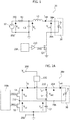
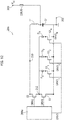
- Figure 1 shows an exemplary pulse generator circuit 20 configured to provide a current pulse to a load 30.
- the pulse generator circuit 20 comprises:
- the load 30 is a laser diode D, i.e. the laser diode D is connected ( e.g. directly) between the terminals 204 and 206.
- the pulse generator circuit 20 is configured as laser diode driver.
- narrow current pulses having rise and fall times in a range between 50 ps (picoseconds) and 300 ps, typically in the range of 100 ps, have to be applied to the diode D.
- a current pulse may be applied to the diode D by closing the electronic switch Q1, whereby the diode D is connected to the supply voltage Vcc.
- a capacitor C 1 is added in order to stabilize the supply voltage Vcc.
- this capacitor C 1 is connected ( e.g. directly) between the input terminals 200 and 202.
- a resistance R 1 connected in series with the capacitor C 1 , which may represent parasitic resistances or a resistor intentionally connected between the terminal 200 and the capacitor C 1 . Accordingly, during a charge phase (switch Q1 opened), the capacitor C 1 is charged (via the resistance R 1 ) to a voltage V 1 corresponding approximately to the supply voltage Vcc. Conversely, when the switch Q1 is closed, the diode D is connected to the capacitor C 1 .
- the respective drive signal DRV for controlling the switching of the electronic switch Q1 may be provided by a control circuit 208 and driver circuit 210.
- the generation of several pulses within a very short time frame is almost impossible with the architecture shown in Figure 1 , because the capacitor C 1 has to be recharged.
- the input voltage Vcc has to be greater than the laser diode drop voltage in order to generate the required di / dt ratio.
- using a supply voltage Vcc being higher than the laser diode voltage drop may generate safety issues in case the switch Q1 is permanently closed, e.g. due to a fault.
- the conductive traces used to connect the diode D to the capacitor C 1 may have associated stray inductances, schematically shown in Figure 1 via an inductance L 1 connected between the load 30 and the capacitor C 1 .
- the stray inductance L 1 cannot be minimized to obtain required di / dt, such as 100ps rise and fall times with a high current pulse amplitude, because the length of the commutation loop is also strongly influenced by capacitances of the circuit, and it is also difficult to obtain a total stray inductance below several nH.
- the maximum obtainable di / dt is usually smaller than 40A/ns and the rise time is often greater than 1 ns.
- this inductance may result in voltage overshoots which may damage the laser diode D.
- one or more of the above objects are achieved by a method of operating a pulse generator circuit having the distinctive elements set forth specifically in the ensuing claims.
- Embodiments moreover concern a related pulse generator circuit and laser system.
- various embodiments of the present disclosure relate to a pulse generator circuit configured to apply a current pulse to a load.
- the pulse generator circuit may be used in a laser system, such as a LiDAR system.
- the pulse generator circuit comprises a positive and a negative input terminal for receiving a supply voltage and two output terminals for providing the current pulse to the load.
- an inductance and a capacitance are connected in series between a first node and the negative input terminal, thereby forming an LC resonant circuit having a given resonant period.
- a charge circuit is configured to charge the capacitance via the supply voltage.
- the inductance such as an inductor
- the capacitance such as a capacitor
- the charge circuit may comprise a resistance, such as a resistor, and optionally an electronic switch connected between the positive supply terminal and an intermediate node between the inductance and the capacitance.
- a first electronic switch is connected between the two output terminals and configured to selectively short-circuit the two output terminals as a function of a first drive signal
- a second electronic switch is configured to selectively connect the two output terminals in parallel with the LC resonant circuit as a function of a second drive signal.
- the first and the second electronic switch may be connected in series between the first node and the negative input terminal, wherein the two output terminals may be connected to the first node and an intermediate node between the first and the second electronic switch.
- the second and the first electronic switch may be connected in series between the first node and the negative input terminal, and the two output terminals may be connected to an intermediate node between the first and the second electronic switch, and the negative input terminal.
- a control circuit is configured to generate the first and the second drive signals. Specifically, in various embodiments, the control circuit is configured to drive the first and second electronic switch during each switching cycle with four switching periods. Specifically, for a first time-interval, the control circuit closes the first electronic switch and opens the second electronic switch, wherein the two output terminals are disconnected from the LC resonant circuit and the capacitance is charged via the charge circuit. For a following second time-interval, the control circuit closes both the first and the second electronic switch, wherein the two output terminals are connected in parallel with the LC resonant circuit and the two output terminals are short-circuited, whereby the LC resonant circuit oscillates with the given resonant period.
- the control circuit opens the first electronic switch and closes the second electronic switch, wherein the two output terminals are connected in parallel with the LC resonant circuit and the LC resonant circuit provides a current to the two output terminals.
- the control circuit closes both the first and the second electronic switch, wherein the two output terminals are connected in parallel with the LC resonant circuit and the two output terminals are short-circuited, whereby the LC resonant circuit oscillates with the given resonant period.
- the control circuit is configured to start the third time-interval when the current provided by the LC resonant circuit reaches (approximately) the given maximum current value.
- the control circuit may be configured to use a (constant) duration for the second time-interval, which is selected in a range between 90% and 110%, preferably between 95% and 105%, of one-fourth (1/4) of the given resonant period.
- the control circuit may be configured to receive data identifying a requested current amplitude to be provided to the two output terminals, and determine the duration of the second time-interval as a function of the data identifying a requested current amplitude.
- the duration of the third time-interval is selected in a range between 500ps and 20ns, preferably between 1 ns and 2 ns.
- the control circuit is configured to start the first time-interval when the current provided by the LC resonant circuit reaches (approximately) zero.
- the duration of the fourth time-interval may be selected such that the sum of the durations of the second, third and fourth time-interval in a range between 90% and 110%, preferably between 95% and 105%, of the given resonant period (or a multiple thereof), and preferably corresponds to the given resonant period (or a multiple thereof).
- the LC oscillator circuit is free to oscillate during the second time-interval and the fourth time-interval.
- the second time- interval is used to set the current flowing through the inductance, which is then provided at the start of the third time-interval to the output terminals.
- the oscillation of the LC resonant circuit itself is used during the fourth time-interval in order to recover the remaining energy stored in the inductance at the end of the third time-interval.
- the current flowing through the inductance becomes negative during the fourth time-interval, thereby charging the capacitance.
- the control circuit is configured to start then the next first time-interval when the current flowing through the inductance reaches then zero.
- the inductance may be in a range between 1 nH (nano-henry) to 1 uH (micro-henry), preferably between 5 and 50 nH, and the capacitance may be in a range between 100 nF (nano-farad) to 10 uF (micro-farad), preferably between 200 and 800 nF.
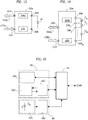
- Figure 2A shows an embodiment of a pulse generator circuit 20a, such as a laser diode driver.
- the pulse generator circuit 20a comprises:
- the load 30 is a laser diode D, i . e . the laser diode D is connected (e.g. directly) between the terminals 204 and 206.
- the pulse generator circuit 20a and optionally the laser diode D may be integrated in an integrated circuit.
- the integrated circuit may comprise two power supply pads (of the die of the integrated circuit) or pins (of a respective package of the integrated circuit) connected to the terminals 200/202, and optionally (if the diode D is not integrated in the integrated circuit) and two further pads or pins for connection to the diode D.
- the pulse generator circuit 20a comprises:
- Figure 2B, 2C, 2D and 2E show possible embodiments of charge circuits 220a, 220b, 220c and 220d.
- the charge circuit 220 is configured to charge the capacitor Cr via the supply voltage Vcc.
- the charge circuit 220 may be connected ( e.g. directly):
- Figure 2B shows an embodiment of a charge circuit 220a, wherein a resistance R is connected ( e.g. directly) between the terminal 200 and the capacitor Cr, e.g. between the terminal 200 and the intermediate node between the inductor Lr and the capacitor Cr.
- the capacitor Cr is charged when the voltage V cr at the capacitor is smaller than the supply voltage Vcc.
- the charge circuit 220 is configured to selectively charge the capacitor Cr when the electronic switch S2 is opened.
- Figure 2C shows an embodiment of a charge circuit 220b, wherein a resistance R and an electronic switch SR are connected ( e.g. directly) in series between the terminal 200 and the capacitor Cr, e.g. between the terminal 200 and the intermediate node between the inductor Lr and the capacitor Cr.
- such an electronic switch SR may be implemented with a controllable electronic switch, such as a FET, or a diode.
- control circuit 208a may be configured to also generate the drive signal for the electronic switch SR.
- this drive signal may correspond to the inverted version of the dive signal DRV2 for the electronic switch S2.
- the resistance R may be a parasitic resistance or may be implemented with a resistor.
- the resistance R is in a range between 0.1 ohm and 300ohm.
- the resistance may also be small ( e.g . between 0.02 Ohm and 10 Ohm), because the electronic switch SR may be used to decouple the LC resonant circuit.
- the resistance R may also correspond to the switch-on resistance of the electronic switch SR.
- the resistance R should be greater (e.g . between 100 Ohm and 300 Ohm) in order to decouple the oscillation of the LC resonant circuit from the supply voltage.
- the inductor Lr and the capacitor Cr may be external with respect to the integrated circuit of the pulse generator circuit 20a.
- the inductor Lr and the capacitor Cr may be connected in series between the pins/pads of such an integrated circuit which are connected to the terminals 204 and 202 of the pulse generator circuit 20a.
- the inductance of the inductor Lr is in a range between 1 nH to 1 uH, preferably between 5 and 50 nH, and the capacitance of the capacitor Cr is in a range between 100 nF to 10 uF, preferably between 200 and 800 nF.
- the electronic switches may be Field-Effect Transistors (FET), such as Metal-Oxide-Semiconductor Field-Effect Transistors (MOSFET) or preferably Gallium nitride (GaN) transistors.
- FET Field-Effect Transistors
- MOSFET Metal-Oxide-Semiconductor Field-Effect Transistors
- GaN Gallium nitride
- the control circuit 208a may be configured to generate drive signals DRV1 and DRV2 for the gate terminals of the FETs S1 and S2.
- the control circuit 208a may comprise FET driver circuits for generating the drive signals DRV1 and DRV2, such as a high-side driver for the FET S1 and a low-side driver circuit for the FET S2.
- the electronic switches S1 and S2 are n-channel FET. Accordingly, in this case, the drain terminal of the FET S1 is connected ( e.g. directly) to the terminal 204/node 210, the source terminal of the FET S1 is connected ( e.g. directly) to the terminal 206/node 212, the drain terminal of the FET S2 is connected ( e.g. directly) to the terminal 206/node 212 and the source terminal of the FET S2 is connected ( e.g. directly) to the terminal 202.
- Figure 4 shows in this respect an embodiment of the drive signals DRV1 and DRV2 generated by the control circuit 208a
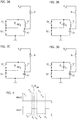
- Figures 3A, 3B, 3C and 3D show the respective switching states of the pulse generator circuit 20a.
- the control circuit 208a closes the first electronic switch S1 (e.g. by setting the signal DRV1 to high) and opens the second electronic switch S2 ( e.g. by setting the signal DRV1 to low), whereby the load 30/diode D is short-circuited.
- the resonant circuit Lr/Cr is connected via the charge circuit 220, such as a resistance R, to the supply voltage Vcc, whereby the capacitor Cr is charged.
- the control circuit 208a closes the first electronic switch S1 ( e.g. by setting the signal DRV1 to high) and closes the second electronic switch S2 ( e.g. by setting the signal DRV1 to high).
- the control circuit 208a opens the first electronic switch S1 ( e.g. by setting the signal DRV1 to low) and closes the second electronic switch S2 ( e.g. by setting the signal DRV1 to high).
- the load 30/diode D is connected in in parallel with the resonant circuit Lr/Cr, and is thus powered via the current i CR flowing through the resonant circuit L r / Cr.
- the time-interval T 3 represents the switch-on interval T ON of the load 30.
- the control circuit 208a closes the first electronic switch S1 ( e.g. by setting the signal DRV1 to high) and closes the second electronic switch S2 ( e.g. by setting the signal DRV1 to high).
- the load 30/diode D and also the resonant circuit Lr/Cr are short circuited, whereby the resonant circuit oscillates with the resonant frequency Fr.
- the control circuit 208a closes the first electronic switch S1 ( e.g. by setting the signal DRV1 to high) and opens the second electronic switch S2 ( e.g. by setting the signal DRV1 to low), whereby the load 30/diode D is short-circuited.
- the resonant circuit Lr/Cr is connected via the charge circuit 220, such as a resistance R, to the supply voltage Vcc, whereby the capacitor Cr is charged.
- control circuit 208a may start a new cycle comprising the phases T 2 , T 3 and T 4 .
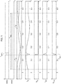
- Figure 5 shows in this respect embodiments of the waveforms of:
- the electronic switches S1 and S2 may be FET. Accordingly, in this case, the current i S1 corresponds to the drain-source current of the FET S1, and the voltage V S1 corresponds to the drain-source voltage of the FET S1. Moreover, Figure 5 shows for this case also a possible waveform of the gate-source voltage V GS1 generated at the gate terminal of the FET S1 in response to the drive signal DRV1.
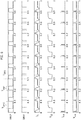
- Figure 6 shows in the context of a plurality of switching cycles embodiments of waveforms of:
- the electronic switch S2 may be opened in this way at zero current, i.e. at the instants when the current i S1 is zero. Moreover, the voltage V Cr reaches in this case its maximum value, thereby improving the recharging of the capacitor Cr.
- an approximate value of the switch-on time T ON2 may be used.
- the actual switch-on time T ON2 ' used by the control circuit 208a may be in a range between 90% and 110% of the "ideal" value T ON2 shown in equation (2), preferably between 95% and 105%.
- the charge circuit 220 such as a resistance R (optionally connected via a switch SR to the capacitor Cr), charges the capacitor Cr during the time interval T 1 substantially to the value of the supply voltage Vcc.
- the time T ON corresponds to the desired laser diode pulse current duration.
- the control unit 208a may select the value of the current i out to be provided to the load 30/laser diode D.
- the actual switch-on time T 2 ' used by the control circuit 208a may be in a range between 90% and 110% of the value T 2 shown in equation (4), preferably between 95% and 105%.
- the time T 2 is constant (even though this time may be settable/programmable) in order to generate pulses with the same current value.
- control circuit 208a When the control circuit 208a then closes the switch S1 at the instant t 3 (end of interval T 3 ), the load 30/laser diode D is short-circuited and the current iout goes to zero. In parallel, the LC resonant circuit continues to oscillate until the control circuit 208a opens the electronic switch S2. As mentioned before, the control unit 208a may open the electronic switch S2 at the instants when the current i CR crosses zero.
- the capacitor Cr is recharged via the charge circuit 220.
- the capacitor Cr may already be recharged in part with the residual energy stored in the resonant loop.
- the inductor Lr essentially implements a current source. This is particularly useful for diodes, such a laser diodes D, insofar as diodes require rather a requested current than a requested voltage. Moreover, this permits that the supply voltage Vcc is smaller than the voltage-drop of the laser diode D because the current i Cr will flow through the diode regardless the value of the voltage-drop.
- Figure 7 shows a possible embodiment of a printed circuit layout adapted to be used to mount the electronic switches S1/S2, the diode D, and the control circuit 208a.
- the electronic switches are FETs.
- the electronic switch S1 comprises a gate terminal GT 1 , at least one source terminal ST 1 and at least one drain terminal DT 1 .
- the electronic switch S2 comprises a gate terminal GT 2 , at least one source terminal ST 2 and at least one drain terminal DT 2 .
- the printed circuit board may comprise:
- the components S1, S2, D and/or 208a may have a respective package with pins or may be mounted directly on the PCB, or by using chip-on-chip technology.
- such electronic switches may have a width W in the range of 1 mm.
- circuit arrangements which comprise:
- Figure 8 shows an embodiment wherein a different connection is used.
- the pulse generator circuit 20a comprises again:
- the output terminals 204 and 206 were connected ( e.g. directly) to the node 210 and the intermediate node 212 between the electronic switches S1 and S2. Accordingly, the (high-side) electronic switch S1 was configured to short-circuit the output terminals 204 and 206, i.e. the load 30, and the (low-side) electronic switch S2 was configured to connect the output terminals 204 and 206, i.e. the load 30, in parallel with the LC resonant circuit.
- the output terminals 204 and 206 are connected ( e.g. directly) to the intermediate node 212 between the electronic switches S1/S2 and the terminal 202, respectively. Accordingly, the low-side switch (connected between the node 212 and the terminal 202) is now configured to short-circuit the output terminals 204 and 206, i.e. the load 30, and corresponds thus now to the electronic switch S1. Conversely, the high-side electronic switch is now configured to connect the output terminals 204 and 206, i.e. the load 30, in parallel with the LC resonant circuit ( i.e. between the node 210 and the terminal 202) and corresponds thus now to the electronic switch S2.
- Figure 10 shows in this respect an embodiment of the drive signals DRV1 and DRV2 generated by the control circuit 208a, and Figures 9A, 9B, 9C show the respective switching states of the pulse generator circuit.
- the drive signals DRV1 and DRV2 generated by the control circuit 208a correspond to the drive signals shown in Figure 4 (except for the voltage levels in order to e.g. generate the required gate-source voltages). Accordingly, the respective description concerning the time-intervals T 1 , T 2 , T 3 and T 4 apply also to the embodiment shown in Figure 8 .
- Figure 9A shows the switching state for the time-interval T 1 (electronic switch S1 closed and electronic switch S2 opened).
- Figure 9B shows the switching state for the time-intervals T 2 and T 4 (electronic switches S1 and S2 closed).
- Figure 9C shows the switching state for the time-interval T 3 (electronic switch S1 opened and electronic switch S2 closed).
- the pulse generator circuit 20a may also be configured to sequentially apply pulses to a plurality of loads, such as a number N of laser diodes D 1 , D 2 ..D N .
- Figure 11 shows an embodiment, wherein the laser diodes D 1 , D 2 ..D N are connected in series between the node 212 and the terminal 202.
- the pulse generator circuit 20a comprises:
- the drive signal DRV2 corresponds to the drive signal DRV2 described in the foregoing.
- the control circuit 208a may be configured to apply the drive signal DRV1 described in the foregoing during each switching cycle to a respective single switch or plurality of switches S1 1 ..S1 N , i.e. in general to a respective subset of the switches S1 1 ..S1 N . Accordingly, a current pulse can be applied to one or more laser diodes D 1 ..D N when one or more switches S1 1 ..S1 N are opened during the time interval T 3 of a given switching cycle.
- the pulse generator circuit 20a may apply a current pulse sequentially to all laser diodes, by opening sequentially during N switching cycles always a different electronic switch S1 1 ..S1 N .
- Figure 12 shows an embodiment, wherein the laser diodes D 1 ..D N are connected in parallel between the node 212 and the terminal 202. Moreover, each electronic switch has connected in series a respective electronic switch S3 1 ..S3 N , i.e. each of the diodes D 1 ..D N is connected with a respective electronic switch S3 1 ..S3 N between the node 212 and the terminal 202.
- the pulse generator circuit 20a comprises again:
- the drive signals DRV1 and DRV2 correspond to the drive signals described in the foregoing, thereby generating during each time interval T 3 of the switching cycles a current pulse.
- the control circuit 208a may be configured to generate the drive signals DRV3 1 ..DRV3 N in order to close during each switching cycle a respective single switch S3 1 ..S3 N or plurality of switches S3 1 ..S3 N . Accordingly, a current pulse can be applied to one or more laser diodes D 1 ..D N when one or more switches S3 1 ..S3 N are closed during the time interval T 3 of a given switching cycle.
- the pulse generator circuit 20a may again apply a current pulse sequentially to all laser diodes, by closing sequentially during N switching cycles always a different electronic switch S3 1 ..S3 N .
- the solutions shown in Figures 11 and 12 may similarly be used when the diodes D 1 ..D N are connected between the node 210 and the node 212.
- the electronic switch S2 could be connected between the node 212 and the terminal 202, and the electronic switches S1 1 ..S1 N could be connected between the node 210 and the node 212, wherein a respective laser diode D 1 ..D N is connected in parallel with each electronic switch S1 1 ..S1 N .
- each of the laser diodes D mentioned in the foregoing could also be implemented with a plurality of laser diodes connected in parallel or preferably in series.
- the pulse generator circuit 20a and optionally the load 30/laser diodes D may be integrated in an integrated circuit.
- Figure 13 shows an embodiment, wherein the integrated circuit comprises pads/pins 204 and 206 for connection to an external diode D.
- Such an integrated circuit may comprise a communication interface 216, such as an Inter-Integrated Circuit (I 2 C) or Serial Peripheral Interface (SPI), connected to one or more pads/pins 214 of the integrated circuit.
- the control circuit 208a may be configured to use this communication interface 216 in order to receive control commands CTRL and/or send diagnostic data DIAG.
- the control commands CTRL may include instruction indicating whether a current pulse should be applied to the diode D and/or data identifying the amplitude of the current pulse, e.g. data identifying the duration of the time interval T 2 .
- the diagnostic data DIAG may comprise data indicating the amplitude of the current pulse applied to the diode D.
- the pulse generator circuit 20a may comprise a current sensor connected in series with the diode D, the switch S2 or with the RC resonant circuit.
- Figure 14 shows that the integrated circuit may also be connected to a plurality of external diodes D 1 ..D N , such as an array or matrix of laser diodes as they are often used in LiDAR systems.
- the integrated circuit comprises a pad/pin 204 and a plurality of pads/pins 206 1 ..206 N for connection to external diodes D 1 ..D N .
- FIG. 15 shows an embodiment of an electronic system comprising a pulse generator circuit 20a as described in the foregoing.
- the electronic system is a LiDAR system comprising:
- control and processing circuit 40 may be configured to exchange data COM with another electronic circuit, such as in order to send the processed data, e.g. data being indicative of the distance of one or more objects from the LiDAR system.
Landscapes
- Physics & Mathematics (AREA)
- General Physics & Mathematics (AREA)
- Condensed Matter Physics & Semiconductors (AREA)
- Electromagnetism (AREA)
- Optics & Photonics (AREA)
- Engineering & Computer Science (AREA)
- Computer Networks & Wireless Communication (AREA)
- Radar, Positioning & Navigation (AREA)
- Remote Sensing (AREA)
- Semiconductor Lasers (AREA)
- Electronic Switches (AREA)
Abstract
- for a first time-interval (T1 ) close the first electronic switch (S1) and open the second electronic switch (S2), wherein the capacitance (Cr) is charged via the charge circuit (220);
- for a following second time-interval (T2 ) close both the first (S1) and the second (S2) electronic switch, wherein the LC resonant circuit (Lr, Cr) oscillates with a given resonant period (Tr);
- for a following third time-interval (T3 , TON ) open the first electronic switch (S1) and close the second electronic switch (S2), wherein the LC resonant circuit (Lr, Cr) provides a current (icr ) to the two output terminals (204, 206); and
- for a following fourth time-interval (T2 ) close both the first (S1) and the second (S2) electronic switch, wherein the LC resonant circuit (Lr, Cr) oscillates with the given resonant period (Tr).
Description
- The embodiments of the present description refer to a pulse generator circuit, such as a pulse generator circuit for laser diodes.
- In many applications it may be required to generate narrow high current pulses.
-
Figure 1 shows an exemplarypulse generator circuit 20 configured to provide a current pulse to aload 30. - In the example considered, the
pulse generator circuit 20 comprises: - a positive and a
negative supply terminal DC voltage source 10, thereby receiving a supply voltage Vcc, - a positive and a
negative output terminal load 30 for providing an output current Iout and an output voltage Vout to theload 30, wherein thepositive output terminal 204 is coupled and typically directly connected to thepositive input terminal 200, and - an electronic switch Q1, such as a Field-Effect Transistor (FET), such as a n-channel FET, configured to selectively connect the
negative output terminal 206 to thenegative input terminal 202. - For example, in
Figure 1 , theload 30 is a laser diode D, i.e. the laser diode D is connected (e.g. directly) between theterminals pulse generator circuit 20 is configured as laser diode driver. For example, in many applications, such as in a Light Detection and Ranging (LiDAR) system, narrow current pulses having rise and fall times in a range between 50 ps (picoseconds) and 300 ps, typically in the range of 100 ps, have to be applied to the diode D. - In the example considered, a current pulse may be applied to the diode D by closing the electronic switch Q1, whereby the diode D is connected to the supply voltage Vcc.
- As shown in
Figure 1 , often a capacitor C1 is added in order to stabilize the supply voltage Vcc. Specifically, typically this capacitor C1 is connected (e.g. directly) between theinput terminals Figure 1 is also shown a resistance R1 connected in series with the capacitor C1, which may represent parasitic resistances or a resistor intentionally connected between theterminal 200 and the capacitor C1. Accordingly, during a charge phase (switch Q1 opened), the capacitor C1 is charged (via the resistance R1) to a voltage V1 corresponding approximately to the supply voltage Vcc. Conversely, when the switch Q1 is closed, the diode D is connected to the capacitor C1. For example, the respective drive signal DRV for controlling the switching of the electronic switch Q1 may be provided by acontrol circuit 208 anddriver circuit 210. - On the one hand, the generation of several pulses within a very short time frame is almost impossible with the architecture shown in
Figure 1 , because the capacitor C1 has to be recharged. On the other hand, the input voltage Vcc has to be greater than the laser diode drop voltage in order to generate the required di/dt ratio. However, using a supply voltage Vcc being higher than the laser diode voltage drop may generate safety issues in case the switch Q1 is permanently closed, e.g. due to a fault. - Moreover, the conductive traces used to connect the diode D to the capacitor C1 may have associated stray inductances, schematically shown in
Figure 1 via an inductance L1 connected between theload 30 and the capacitor C1. Often the stray inductance L1 cannot be minimized to obtain required di/dt, such as 100ps rise and fall times with a high current pulse amplitude, because the length of the commutation loop is also strongly influenced by capacitances of the circuit, and it is also difficult to obtain a total stray inductance below several nH. For this reason, the maximum obtainable di/dt is usually smaller than 40A/ns and the rise time is often greater than 1 ns. Moreover, this inductance may result in voltage overshoots which may damage the laser diode D. - The above issues also imply that the value of the output current Iout provided to the laser diode D is difficult to be controlled, because the current Iout depends on the impedance of the commutation loop. For example, a parasitic output capacitance of the
laser driver circuit 20 may enlarge the real current pulse seen by the laser diode D. - Considering the foregoing, it is therefore an object of various embodiments to provide improved solutions for pulse generator circuits.
- According to one or more embodiments, one or more of the above objects are achieved by a method of operating a pulse generator circuit having the distinctive elements set forth specifically in the ensuing claims. Embodiments moreover concern a related pulse generator circuit and laser system.
- The claims form an integral part of the technical teaching of the description provided herein.
- As mentioned before, various embodiments of the present disclosure relate to a pulse generator circuit configured to apply a current pulse to a load. For example, the pulse generator circuit may be used in a laser system, such as a LiDAR system.
- In various embodiments, the pulse generator circuit comprises a positive and a negative input terminal for receiving a supply voltage and two output terminals for providing the current pulse to the load. In various embodiments, an inductance and a capacitance are connected in series between a first node and the negative input terminal, thereby forming an LC resonant circuit having a given resonant period. In various embodiments, a charge circuit is configured to charge the capacitance via the supply voltage. For example, in various embodiments, the inductance, such as an inductor, is connected to the first node and the capacitance, such as a capacitor, is connected to the negative input terminal. In this case, the charge circuit may comprise a resistance, such as a resistor, and optionally an electronic switch connected between the positive supply terminal and an intermediate node between the inductance and the capacitance.
- In various embodiments, a first electronic switch is connected between the two output terminals and configured to selectively short-circuit the two output terminals as a function of a first drive signal, and a second electronic switch is configured to selectively connect the two output terminals in parallel with the LC resonant circuit as a function of a second drive signal. For example, the first and the second electronic switch may be connected in series between the first node and the negative input terminal, wherein the two output terminals may be connected to the first node and an intermediate node between the first and the second electronic switch. Alternatively, the second and the first electronic switch may be connected in series between the first node and the negative input terminal, and the two output terminals may be connected to an intermediate node between the first and the second electronic switch, and the negative input terminal.
- In various embodiments, a control circuit is configured to generate the first and the second drive signals. Specifically, in various embodiments, the control circuit is configured to drive the first and second electronic switch during each switching cycle with four switching periods. Specifically, for a first time-interval, the control circuit closes the first electronic switch and opens the second electronic switch, wherein the two output terminals are disconnected from the LC resonant circuit and the capacitance is charged via the charge circuit. For a following second time-interval, the control circuit closes both the first and the second electronic switch, wherein the two output terminals are connected in parallel with the LC resonant circuit and the two output terminals are short-circuited, whereby the LC resonant circuit oscillates with the given resonant period. For a following third time-interval, the control circuit opens the first electronic switch and closes the second electronic switch, wherein the two output terminals are connected in parallel with the LC resonant circuit and the LC resonant circuit provides a current to the two output terminals. For a following fourth time-interval, the control circuit closes both the first and the second electronic switch, wherein the two output terminals are connected in parallel with the LC resonant circuit and the two output terminals are short-circuited, whereby the LC resonant circuit oscillates with the given resonant period.
- Accordingly, during the second time-interval, the current provided by the LC resonant circuit oscillates with a given maximum current value. In various embodiments, the control circuit is configured to start the third time-interval when the current provided by the LC resonant circuit reaches (approximately) the given maximum current value. For example, the control circuit may be configured to use a (constant) duration for the second time-interval, which is selected in a range between 90% and 110%, preferably between 95% and 105%, of one-fourth (1/4) of the given resonant period. Alternatively, the control circuit may be configured to receive data identifying a requested current amplitude to be provided to the two output terminals, and determine the duration of the second time-interval as a function of the data identifying a requested current amplitude.
- In various embodiments, the duration of the third time-interval is selected in a range between 500ps and 20ns, preferably between 1 ns and 2 ns.
- In various embodiments, the control circuit is configured to start the first time-interval when the current provided by the LC resonant circuit reaches (approximately) zero. For example, the duration of the fourth time-interval may be selected such that the sum of the durations of the second, third and fourth time-interval in a range between 90% and 110%, preferably between 95% and 105%, of the given resonant period (or a multiple thereof), and preferably corresponds to the given resonant period (or a multiple thereof).
- Accordingly, in various embodiments, the LC oscillator circuit is free to oscillate during the second time-interval and the fourth time-interval. Specifically, the second time- interval is used to set the current flowing through the inductance, which is then provided at the start of the third time-interval to the output terminals. Moreover, the oscillation of the LC resonant circuit itself is used during the fourth time-interval in order to recover the remaining energy stored in the inductance at the end of the third time-interval. Specifically, for this purpose, in various embodiments, the current flowing through the inductance becomes negative during the fourth time-interval, thereby charging the capacitance. Preferably, the control circuit is configured to start then the next first time-interval when the current flowing through the inductance reaches then zero.
- For example, in various embodiments, the inductance may be in a range between 1 nH (nano-henry) to 1 uH (micro-henry), preferably between 5 and 50 nH, and the capacitance may be in a range between 100 nF (nano-farad) to 10 uF (micro-farad), preferably between 200 and 800 nF.
- The embodiments of the present disclosure will now be described with reference to the annexed plates of drawings, which are provided purely to way of non-limiting example and in which:
The features and advantages of the present invention will become apparent from the following detailed description of practical embodiments thereof, shown by way of non-limiting example in the accompanying drawings, in which: -
Figure 1 shows a circuit schematic of a pulse generator circuit; -
Figures 2A ,2B, 2C, 2D and 2E show a circuit schematic of a first embodiment of a pulse generator circuit; -
Figures 3A, 3B, 3C and 3D show embodiments of the switching states of the pulse generator circuit ofFigure 2 ; -
Figure 4 shows an embodiment of drive signals used in the pulse generator circuit ofFigure 2 ; -
Figures 5 and6 shows exemplary waveforms of the pulse generator circuit ofFigure 2 ; -
Figure 7 shows schematically an embodiment of an integrated circuit layout able to implement the pulse generator circuit ofFigure 2 ; -
Figure 8 shows a circuit schematic of a second embodiment of a pulse generator circuit; -
Figures 9A, 9B and 9C shows embodiments of the switching states of the pulse generator circuit ofFigure 8 ; -
Figure 10 shows an embodiment of drive signals used in the pulse generator circuit ofFigure 8 ; -
Figure 11 shows a circuit schematic of a third embodiment of a pulse generator circuit; -
Figure 12 shows a circuit schematic of a fourth embodiment of a pulse generator circuit; -
Figures 13 and 14 show embodiments of integrated circuits comprising a pulse generator circuit according to the present disclosure; and -
Figure 15 shows a laser system comprising one or more pulse generator circuits according to the present disclosure. - In the ensuing description, various specific details are illustrated aimed at enabling an in-depth understanding of the embodiments. The embodiments may be provided without one or more of the specific details, or with other methods, components, materials, etc. In other cases, known structures, materials, or operations are not shown or described in detail so that various aspects of the embodiments will not be obscured.
- Reference to "an embodiment" or "one embodiment" in the framework of this description is meant to indicate that a particular configuration, structure, or characteristic described in relation to the embodiment is comprised in at least one embodiment. Hence, phrases such as "in an embodiment", "in one embodiment", or the like that may be present in various points of this description do not necessarily refer to one and the same embodiment. Moreover, particular conformations, structures, or characteristics may be combined in any adequate way in one or more embodiments.
- The references used herein are only provided for convenience and hence do not define the sphere of protection or the scope of the embodiments.
- In
Figures 2 to 15 described below, parts, elements or components that have already been described with reference toFigure 1 are designated by the same references used previously in these figures. The description of these elements has already been made and will not be repeated in what follows in order not to burden the present detailed description. -
Figure 2A shows an embodiment of apulse generator circuit 20a, such as a laser diode driver. - In the embodiment considered, the
pulse generator circuit 20a comprises: - a positive and a
negative supply terminal negative terminal 202 represents a reference voltage, such as ground; and - a positive and a
negative output terminal load 30 for providing an output current Iout to theload 30. - For example, in various embodiments, the
load 30 is a laser diode D, i.e. the laser diode D is connected (e.g. directly) between theterminals pulse generator circuit 20a and optionally the laser diode D may be integrated in an integrated circuit. Accordingly, in this case, the integrated circuit may comprise two power supply pads (of the die of the integrated circuit) or pins (of a respective package of the integrated circuit) connected to theterminals 200/202, and optionally (if the diode D is not integrated in the integrated circuit) and two further pads or pins for connection to the diode D. - In the embodiment considered, the
pulse generator circuit 20a comprises: - an LC resonant circuit comprising an inductor Lr and a capacitor Cr connected (e.g. directly) in series between a
node 210 and the terminal 202, wherein e.g. the inductor Lr is connected to thenode 210 and the capacitor Cr is connected to the terminal 202; - a
charge circuit 220 configured to charge the capacitor Cr; - a first electronic switch S1 (having a current-path) connected (e.g. directly) between the
node 210 and anode 212 connected (e.g. directly) to the terminal 206, i.e. the electronic switch S1 is connected in parallel with theload 30 and is thus configured to selectively short-circuit theoutput terminals 204/206, i.e. theload 30; and - a second electronic S2 (having a current-path) connected (e.g. directly) in series between the
node 212 and the terminal 202, i.e. the second electronic S2 is configured to selectively connect theoutput terminals 204/206, i.e. theload 30, in parallel with the LC resonant circuit Lr/Cr; and - a
control circuit 208a configured to generate drive signals DRV1 and DRV2 for the control terminals of the electronic switches S1 and S2. - For example,
Figure 2B, 2C, 2D and 2E show possible embodiments ofcharge circuits - In general, the
charge circuit 220 is configured to charge the capacitor Cr via the supply voltage Vcc. For example, thecharge circuit 220 may be connected (e.g. directly): - between the terminal 200 and the
node 210, thereby charging the capacitor Cr through the inductor Lr, or - preferably, between the terminal 200 and the intermediate node between the
node 210, thereby directly charging the capacitor Cr. - For example,
Figure 2B shows an embodiment of acharge circuit 220a, wherein a resistance R is connected (e.g. directly) between the terminal 200 and the capacitor Cr, e.g. between the terminal 200 and the intermediate node between the inductor Lr and the capacitor Cr. - Thus, in this case, the capacitor Cr is charged when the voltage Vcr at the capacitor is smaller than the supply voltage Vcc.
- In various embodiments, the
charge circuit 220 is configured to selectively charge the capacitor Cr when the electronic switch S2 is opened. - For example,
Figure 2C shows an embodiment of acharge circuit 220b, wherein a resistance R and an electronic switch SR are connected (e.g. directly) in series between the terminal 200 and the capacitor Cr, e.g. between the terminal 200 and the intermediate node between the inductor Lr and the capacitor Cr. - As shown in
Figures 2D and 2E , such an electronic switch SR may be implemented with a controllable electronic switch, such as a FET, or a diode. - Accordingly, the
control circuit 208a may be configured to also generate the drive signal for the electronic switch SR. For example, this drive signal may correspond to the inverted version of the dive signal DRV2 for the electronic switch S2. - In various embodiments, the resistance R may be a parasitic resistance or may be implemented with a resistor. For example, in various embodiments the resistance R is in a range between 0.1 ohm and 300ohm. In general, when the electronic switch SR is used, the resistance may also be small (e.g. between 0.02 Ohm and 10 Ohm), because the electronic switch SR may be used to decouple the LC resonant circuit. For example, in this case, the resistance R may also correspond to the switch-on resistance of the electronic switch SR. Conversely, in the absence of an electronic switch SR, the resistance R should be greater (e.g. between 100 Ohm and 300 Ohm) in order to decouple the oscillation of the LC resonant circuit from the supply voltage.
- In various embodiments, the inductor Lr and the capacitor Cr may be external with respect to the integrated circuit of the
pulse generator circuit 20a. For example, the inductor Lr and the capacitor Cr may be connected in series between the pins/pads of such an integrated circuit which are connected to theterminals pulse generator circuit 20a. - In various embodiments the inductance of the inductor Lr is in a range between 1 nH to 1 uH, preferably between 5 and 50 nH, and the capacitance of the capacitor Cr is in a range between 100 nF to 10 uF, preferably between 200 and 800 nF.
- In various embodiments, the electronic switches may be Field-Effect Transistors (FET), such as Metal-Oxide-Semiconductor Field-Effect Transistors (MOSFET) or preferably Gallium nitride (GaN) transistors. Accordingly, the
control circuit 208a may be configured to generate drive signals DRV1 and DRV2 for the gate terminals of the FETs S1 and S2. For this purpose, thecontrol circuit 208a may comprise FET driver circuits for generating the drive signals DRV1 and DRV2, such as a high-side driver for the FET S1 and a low-side driver circuit for the FET S2. - For example, in various embodiments, the electronic switches S1 and S2 are n-channel FET. Accordingly, in this case, the drain terminal of the FET S1 is connected (e.g. directly) to the terminal 204/
node 210, the source terminal of the FET S1 is connected (e.g. directly) to the terminal 206/node 212, the drain terminal of the FET S2 is connected (e.g. directly) to the terminal 206/node 212 and the source terminal of the FET S2 is connected (e.g. directly) to the terminal 202. -
Figure 4 shows in this respect an embodiment of the drive signals DRV1 and DRV2 generated by thecontrol circuit 208a, andFigures 3A, 3B, 3C and 3D show the respective switching states of thepulse generator circuit 20a. - Specifically, during/for a first time-interval T1 (see also
Figure 3A ), thecontrol circuit 208a closes the first electronic switch S1 (e.g. by setting the signal DRV1 to high) and opens the second electronic switch S2 (e.g. by setting the signal DRV1 to low), whereby theload 30/diode D is short-circuited. Moreover, the resonant circuit Lr/Cr is connected via thecharge circuit 220, such as a resistance R, to the supply voltage Vcc, whereby the capacitor Cr is charged. - At an instant t1 (end of the interval T1 ) the
control circuit 208a closes the first electronic switch S1 (e.g. by setting the signal DRV1 to high) and closes the second electronic switch S2 (e.g. by setting the signal DRV1 to high). Thus, during/for a following second time-interval T2 (see alsoFigure 3B ) theload 30/diode D is short-circuited, and also the resonant circuit Lr/Cr is short circuited, which thus oscillates with a given resonant frequency Fr:
- At an instant t2 (end of the interval T2 ) the
control circuit 208a opens the first electronic switch S1 (e.g. by setting the signal DRV1 to low) and closes the second electronic switch S2 (e.g. by setting the signal DRV1 to high). Thus, during/for a following third time-interval T3 (see alsoFigure 3C ), theload 30/diode D is connected in in parallel with the resonant circuit Lr/Cr, and is thus powered via the current iCR flowing through the resonant circuit Lr/Cr. Thus, the time-interval T3 represents the switch-on interval TON of theload 30. - At an instant t3 (end of the interval T3 ) the
control circuit 208a closes the first electronic switch S1 (e.g. by setting the signal DRV1 to high) and closes the second electronic switch S2 (e.g. by setting the signal DRV1 to high). Thus, during/for a following fourth time-interval T4 (see alsoFigure 3D ), theload 30/diode D and also the resonant circuit Lr/Cr are short circuited, whereby the resonant circuit oscillates with the resonant frequency Fr. - At an instant t4 (end of the interval T4 ) the
control circuit 208a closes the first electronic switch S1 (e.g. by setting the signal DRV1 to high) and opens the second electronic switch S2 (e.g. by setting the signal DRV1 to low), whereby theload 30/diode D is short-circuited. Moreover, the resonant circuit Lr/Cr is connected via thecharge circuit 220, such as a resistance R, to the supply voltage Vcc, whereby the capacitor Cr is charged. - Thus, by closing the electronic switch S2 after a time-interval T1 /at a next instant t'1 the
control circuit 208a may start a new cycle comprising the phases T2, T3 and T4. -
Figure 5 shows in this respect embodiments of the waveforms of: - the drive signals DRV1 and DRV2,
- the voltage VCr at the capacitor Cr and the current iCr flowing through the capacitor Cr, i.e. the current flowing through the LC resonant circuit;
- the current iS1 flowing through the (current path) of the electronic switch S1;
- the voltage VS1 at the electronic switch S1;
- the output current iout, i.e. the current flowing through the
load 30/laser diode D. - As mentioned before, in various embodiments, the electronic switches S1 and S2 may be FET. Accordingly, in this case, the current iS1 corresponds to the drain-source current of the FET S1, and the voltage VS1 corresponds to the drain-source voltage of the FET S1. Moreover,
Figure 5 shows for this case also a possible waveform of the gate-source voltage VGS1 generated at the gate terminal of the FET S1 in response to the drive signal DRV1. -
Figure 6 shows in the context of a plurality of switching cycles embodiments of waveforms of: - the drive signals DRV1 and DRV2,
- the current iS1 flowing through the (current path) of the electronic switch S1;
- the voltage VS2 at the electronic switch S1;
- the output current iout, i.e. the current flowing through the
load 30/laser diode D. - the output voltage Vout, i.e. the voltage at the
load 30/laser diode D. - Thus, in the embodiments described with respect to the operation shown in
Figures 5 and6 , the drive signals DRV1 and DRV2 are pulsed signals having given switching durations Tsw1 = TON1 + TOFF1 and TSW2 = TON2 + TOFF2, with TSW1 = TSW2. Specifically, in various embodiments: - the switch-on time TON1 of the switch S1 (e.g. when the drive signal DRV1 is set to high) corresponds to T1 + T2 + T4, and the switch-off time TOFF1 of the switch S1 (e.g. when the drive signal DRV1 is set to low) corresponds to T3 = TON; and
- the switch-on time TON2 of the switch S2 (e.g. when the drive signal DRV2 is set to high) corresponds to T2 + T3 + T4, and the switch-off time TOFF2 of the switch S2 (e.g. when the drive signal DRV2 is set to low) corresponds to T1 .
- In various embodiments, the switch-on time TON2 of the electronic switch S2 corresponds (approximately) to a multiple of a period Tr = 1/Fr of the oscillation, i.e.:

- The inventors have observed that the electronic switch S2 may be opened in this way at zero current, i.e. at the instants when the current iS1 is zero. Moreover, the voltage VCr reaches in this case its maximum value, thereby improving the recharging of the capacitor Cr. Generally, also an approximate value of the switch-on time TON2 may be used. For example, in various embodiments, the actual switch-on time TON2 ' used by the
control circuit 208a may be in a range between 90% and 110% of the "ideal" value TON2 shown in equation (2), preferably between 95% and 105%. - Thus, in various embodiments, the
charge circuit 220, such as a resistance R (optionally connected via a switch SR to the capacitor Cr), charges the capacitor Cr during the time interval T1 substantially to the value of the supply voltage Vcc. - Next, the
control unit 208a closes the switch S2 for a duration TON2 close to 1/Fr (or a multiple thereof), where Fr = 1/(2 π Lr Cr) is the resonant frequency of the LC resonant circuit. Accordingly, the values Vcc, Lr and Cr define the resonant peak current imax flowing through the LC resonant tank:
- The
control unit 208a opens then the switch S1 for the time-interval TOFF1 = T3 = TON. For example, in various embodiments, the time TON corresponds to the desired laser diode pulse current duration. Specifically, when the electronic switch S1 is opened, the current provided by the LC resonant circuit is forced to flow immediately through theoutput terminals 204/206, i.e. theload 30/laser diode D. - Thus, by controlling the duration of the interval T2, the
control unit 208a may select the value of the current iout to be provided to theload 30/laser diode D. For example, in various embodiments, the duration of the time interval T2 corresponds to the instants when the resonant current iCr reaches its peak value imax, e.g.:
- Generally, also an approximate value of the above time T2 may be used. For example, in various embodiments, the actual switch-on time T2 ' used by the
control circuit 208a may be in a range between 90% and 110% of the value T2 shown in equation (4), preferably between 95% and 105%. - In various embodiments, the time T2 is constant (even though this time may be settable/programmable) in order to generate pulses with the same current value.
- When the
control circuit 208a then closes the switch S1 at the instant t3 (end of interval T3 ), theload 30/laser diode D is short-circuited and the current iout goes to zero. In parallel, the LC resonant circuit continues to oscillate until thecontrol circuit 208a opens the electronic switch S2. As mentioned before, thecontrol unit 208a may open the electronic switch S2 at the instants when the current iCR crosses zero. - Once the electronic switch S2 is opened, the capacitor Cr is recharged via the
charge circuit 220. As mentioned before, due to the additional time interval T4 (which permits to obtain a duration TON2 close to 1/Fr) the capacitor Cr may already be recharged in part with the residual energy stored in the resonant loop. - Accordingly, in the embodiment considered, the inductor Lr essentially implements a current source. This is particularly useful for diodes, such a laser diodes D, insofar as diodes require rather a requested current than a requested voltage. Moreover, this permits that the supply voltage Vcc is smaller than the voltage-drop of the laser diode D because the current iCr will flow through the diode regardless the value of the voltage-drop.
-
Figure 7 shows a possible embodiment of a printed circuit layout adapted to be used to mount the electronic switches S1/S2, the diode D, and thecontrol circuit 208a. - In the embodiment considered, the electronic switches are FETs. Specifically, the electronic switch S1 comprises a gate terminal GT1, at least one source terminal ST1 and at least one drain terminal DT1. Similarly, the electronic switch S2 comprises a gate terminal GT2, at least one source terminal ST2 and at least one drain terminal DT2.
- Accordingly, the printed circuit board may comprise:
- a first metallic area/track MA1 for connecting the gate terminal GT1 to the terminal of the
control circuit 208a providing the drive signal DRV1; - a second metallic area/track MA2 for connecting the drain terminal DT1 to the terminal 204/anode of the diode D;
- a third metallic area/track MA1 for connecting the source terminal ST1 to the terminal 206/cathode of the diode D and the drain terminal DT2;
- a fourth metallic area/track MA4 for connecting the gate terminal GT2 to the terminal of the
control circuit 208a providing the drive signal DRV2; and - a fifth metallic area/track MA5 for connecting the source terminal ST2 to the terminal 202, such as a ground pin of the
control circuit 208a. - In general, the components S1, S2, D and/or 208a may have a respective package with pins or may be mounted directly on the PCB, or by using chip-on-chip technology. For example, just to provide a dimensional reference, such electronic switches (without package) may have a width W in the range of 1 mm.
- Generally, also other circuit arrangements may be used, which comprise:
- an LC resonant circuit comprising an inductor Lr and a capacitor Cr connected in series;
- a charge circuit 229 configured to charge the capacitor Cr via the supply voltage Vcc, such as the resistor R and/or an electronic switch SR connected between the supply voltage Vcc and the capacitor Cr;
- a first electronic switch S1 configured to selectively short-circuit the output terminals, i.e. the
load 30/laser diode D; - a second electronic switch S2 configured to selectively connect the output terminals, i.e. the
load 30/laser diode D, to the LC resonant circuit; and - a
control circuit 208a configured to control the switching of the first and second electronic switch S1 and S2 with the following sequence of time intervals:- during a first time-interval T1, close the first electronic switch S1 and open the second electronic switch S2;
- during a second time-interval T2 , close the first electronic switch S1 and close the second electronic switch S2;
- during a third time-interval T1, open the first electronic switch S1 and close the second electronic switch S2; and
- during a fourth time-interval T4, close the first electronic switch S1 and close the second electronic switch S2.
- For example,
Figure 8 shows an embodiment wherein a different connection is used. - Specifically, in the embodiment considered, the
pulse generator circuit 20a comprises again: - a positive and a
negative supply terminal negative terminal 202 represents again a reference voltage, such as ground; - a positive and a
negative output terminal load 30 for providing an output current Iout to theload 30/laser diode D; - an LC resonant circuit comprising an inductor Lr and a capacitor Cr connected (e.g. directly) in series between a
node 210 and the terminal 202; - a
charge circuit 220, e.g., implemented with a resistance R connected (e.g. directly) between the terminal 200 and the intermediate node between the inductor Lr and the capacitor Cr; - two electronic switches S1 and S2, such as (n-channel) FET, connected (e.g. directly) between the
node 210 and the terminal 202. - In
Figure 2 , theoutput terminals node 210 and theintermediate node 212 between the electronic switches S1 and S2. Accordingly, the (high-side) electronic switch S1 was configured to short-circuit theoutput terminals load 30, and the (low-side) electronic switch S2 was configured to connect theoutput terminals load 30, in parallel with the LC resonant circuit. - Conversely, in the embodiment considered, the
output terminals intermediate node 212 between the electronic switches S1/S2 and the terminal 202, respectively. Accordingly, the low-side switch (connected between thenode 212 and the terminal 202) is now configured to short-circuit theoutput terminals load 30, and corresponds thus now to the electronic switch S1. Conversely, the high-side electronic switch is now configured to connect theoutput terminals load 30, in parallel with the LC resonant circuit (i.e. between thenode 210 and the terminal 202) and corresponds thus now to the electronic switch S2. -
Figure 10 shows in this respect an embodiment of the drive signals DRV1 and DRV2 generated by thecontrol circuit 208a, andFigures 9A, 9B, 9C show the respective switching states of the pulse generator circuit. - Specifically, as shown in
Figure 10 , the drive signals DRV1 and DRV2 generated by thecontrol circuit 208a correspond to the drive signals shown inFigure 4 (except for the voltage levels in order to e.g. generate the required gate-source voltages). Accordingly, the respective description concerning the time-intervals T1 , T2, T3 and T4 apply also to the embodiment shown inFigure 8 . - For example,
Figure 9A shows the switching state for the time-interval T1 (electronic switch S1 closed and electronic switch S2 opened).Figure 9B shows the switching state for the time-intervals T2 and T4 (electronic switches S1 and S2 closed). Finally,Figure 9C shows the switching state for the time-interval T3 (electronic switch S1 opened and electronic switch S2 closed). - In various embodiments, the
pulse generator circuit 20a may also be configured to sequentially apply pulses to a plurality of loads, such as a number N of laser diodes D1, D2..DN. - For example,
Figure 11 shows an embodiment, wherein the laser diodes D1, D2..DN are connected in series between thenode 212 and the terminal 202. - In the embodiment considered, the
pulse generator circuit 20a comprises: - a positive and a
negative supply terminal negative terminal 202 represents again a reference voltage, such as ground; - an LC resonant circuit comprising an inductor Lr and a capacitor Cr connected (e.g. directly) in series between the
node 210 and the terminal 202; - a
charge circuit 220, e.g., implemented with a resistance R connected (e.g. directly) between the terminal 200 and the intermediate node between the inductor Lr and the capacitor Cr; - an electronic switch S2 configured to connected the
node 212 to the LC resonant circuit, i.e. the electronic switch S2 is configured to connected the series connection of laser diodes D1, D2..DN in parallel with the LC resonant circuit, i.e. between thenode 210 and the terminal 202; - N electronic switches S11..S1N, wherein each of the N electronic switches S11..S1N is configured to short-circuit a respective laser diode D1..DN;
- a
control circuit 208a configured to generate the drive signal DRV2 for the electronic switch S2 and drive signals DRV11..DRV1N for the electronic switches S11..S1N. - Specifically, in the embodiment considered, the drive signal DRV2 corresponds to the drive signal DRV2 described in the foregoing. Moreover, the
control circuit 208a may be configured to apply the drive signal DRV1 described in the foregoing during each switching cycle to a respective single switch or plurality of switches S11..S1N, i.e. in general to a respective subset of the switches S11..S1N. Accordingly, a current pulse can be applied to one or more laser diodes D1..DN when one or more switches S11..S1N are opened during the time interval T3 of a given switching cycle. With this solution it is thus possible to apply a current pulse to a plurality of laser diodes either at the same time or during different switching cycles. For example, in the way thepulse generator circuit 20a may apply a current pulse sequentially to all laser diodes, by opening sequentially during N switching cycles always a different electronic switch S11..S1N. - Conversely,
Figure 12 shows an embodiment, wherein the laser diodes D1..DN are connected in parallel between thenode 212 and the terminal 202. Moreover, each electronic switch has connected in series a respective electronic switch S31..S3N, i.e. each of the diodes D1..DN is connected with a respective electronic switch S31..S3N between thenode 212 and the terminal 202. - In the embodiment considered, the
pulse generator circuit 20a comprises again: - a positive and a
negative supply terminal negative terminal 202 represents again a reference voltage, such as ground; - an LC resonant circuit comprising an inductor Lr and a capacitor Cr connected (e.g. directly) in series between a
node 210 and the terminal 202; - a
charge circuit 220, e.g., implemented with a resistance R connected (e.g. directly) between the terminal 200 and the intermediate node between the inductor Lr and the capacitor Cr; - an electronic switch S2 configured to connected the
node 212 to the LC resonant circuit, i.e. the electronic switch S2 is configured to connect the parallel connection of laser diodes D1, D2..DN in parallel with the LC resonant circuit, i.e. between thenode 210 and the terminal 202; - an electronic switch S1 configured to short-circuit the parallel connection of laser diode D1..DN; and
- a
control circuit 208a configured to generate the drive signals DRV1 and DRV2 for the electronic switches S1 and S2 and drive signals DRV31..DRV3N for the electronic switches S31..S3N. - Specifically, in the embodiment considered, the drive signals DRV1 and DRV2 correspond to the drive signals described in the foregoing, thereby generating during each time interval T3 of the switching cycles a current pulse. Moreover, the
control circuit 208a may be configured to generate the drive signals DRV31..DRV3N in order to close during each switching cycle a respective single switch S31..S3N or plurality of switches S31..S3N. Accordingly, a current pulse can be applied to one or more laser diodes D1..DN when one or more switches S31..S3N are closed during the time interval T3 of a given switching cycle. With this solution it is thus again possible to apply a current pulse to a plurality of laser diodes either at the same time or with different timing. For example, in the way thepulse generator circuit 20a may again apply a current pulse sequentially to all laser diodes, by closing sequentially during N switching cycles always a different electronic switch S31..S3N. - In general, the solutions shown in
Figures 11 and12 may similarly be used when the diodes D1..DN are connected between thenode 210 and thenode 212. In this case, only the position of the electronic switches S1 and S2 have to be inverted. For example, for the case shown inFigure 11 , the electronic switch S2 could be connected between thenode 212 and the terminal 202, and the electronic switches S11..S1N could be connected between thenode 210 and thenode 212, wherein a respective laser diode D1..DN is connected in parallel with each electronic switch S11..S1N. - In general, each of the laser diodes D mentioned in the foregoing could also be implemented with a plurality of laser diodes connected in parallel or preferably in series.
- As described in the foregoing, the
pulse generator circuit 20a and optionally theload 30/laser diodes D may be integrated in an integrated circuit. - For example,
Figure 13 shows an embodiment, wherein the integrated circuit comprises pads/pins 204 and 206 for connection to an external diode D. - Moreover,
Figure 13 highlights that such an integrated circuit may comprise acommunication interface 216, such as an Inter-Integrated Circuit (I2C) or Serial Peripheral Interface (SPI), connected to one or more pads/pins 214 of the integrated circuit. For example, thecontrol circuit 208a may be configured to use thiscommunication interface 216 in order to receive control commands CTRL and/or send diagnostic data DIAG. For example, the control commands CTRL may include instruction indicating whether a current pulse should be applied to the diode D and/or data identifying the amplitude of the current pulse, e.g. data identifying the duration of the time interval T2 . Conversely, the diagnostic data DIAG may comprise data indicating the amplitude of the current pulse applied to the diode D. For example, for this purpose thepulse generator circuit 20a may comprise a current sensor connected in series with the diode D, the switch S2 or with the RC resonant circuit. - Similarly,
Figure 14 shows that the integrated circuit may also be connected to a plurality of external diodes D1..DN, such as an array or matrix of laser diodes as they are often used in LiDAR systems. For example, inFigure 14 , the integrated circuit comprises a pad/pin 204 and a plurality of pads/pins 2061..206N for connection to external diodes D1..DN. -
Figure 15 shows an embodiment of an electronic system comprising apulse generator circuit 20a as described in the foregoing. Specifically, in the embodiment considered, the electronic system is a LiDAR system comprising: - a
transmitter portion 42 comprising:- one or more
pulse generator circuits 20a configured to apply current pulses to a plurality of laser diodes, e.g. according to a given timing scheme; - a Micro-Electro-Mechanical Systems (MEMS)
mirror 420 having associated arespective control circuit 422 in order to send actuation commands to theMEMS mirror 420 and optionally to receive position data from theMEMS mirror 420;
- one or more
- a
receiver portion 44 comprising a plurality ofoptical sensors 440, such as photo diodes DR, configured to provide a signal to arespective measurement circuit 442; and - a control and
processing circuit 40 configured to provide control information to thepulse generator circuits 20a and thecontrol circuit 422 associated with theMEMS mirror 420, and to receive and process the data received from themeasurement circuit 440. - In various embodiment, the control and
processing circuit 40 may be configured to exchange data COM with another electronic circuit, such as in order to send the processed data, e.g. data being indicative of the distance of one or more objects from the LiDAR system. - Accordingly, one or more of the described embodiments have the following advantages:
- a fast switching with rise and fall times in the lOOps range may be obtained, which permits the generation of current pulses with a duration in the 1ns range (e.g. the duration of the time-interval T3 may be selected in a range between 500ps and 20ns, preferably between 1 ns and 2 ns) with a current amplitude imax selected in a range between 5A and 200A, preferably between 10A and 50A.
- an easy control of the amplitude of the current pulse is possible by adapting the duration of the time interval T2 ;
- the switching loop may be implemented directly in an integrated circuit, which permits to reduce parasitic inductances inside the commutation loop, e.g. below 0.1nH; and
- the value of the supply voltage Vcc may be smaller than laser diode voltage drop.
- Of course, without prejudice to the principle of the invention, the details of construction and the embodiments may vary widely with respect to what has been described and illustrated herein purely by way of example, without thereby departing from the scope of the present invention, as defined by the ensuing claims.
Claims (15)
- A method of operating a pulse generator circuit (20a) configured to apply a current pulse to a load (30), wherein said pulse generator circuit (20a) comprises:- a positive (200) and a negative (202) input terminal for receiving a supply voltage (Vcc);- two output terminals (204, 206) for providing said current pulse to said load (30);- an LC resonant circuit (Lr, Cr) comprising an inductance (Lr) and a capacitance (Cr) connected in series between a first node (210) and said negative input terminal (202), wherein said LC resonant circuit (Lr, Cr) has a given resonant period (Tr);- a charge circuit (220) configured to charge said capacitance (Cr) via said supply voltage (Vcc);- a first electronic switch (S1) connected between said two output terminals (204, 206) and configured to selectively short-circuit said two output terminals (204, 206) as a function of a first drive signal (DRV1); and- a second electronic switch (S2) configured to selectively connect said two output terminals (204, 206) in parallel with said LC resonant circuit (Lr, Cr) as a function of a second drive signal (DRV2);
wherein the method comprises generating said first (DRV1) and said second (DRV2) drive signals in order to repeat the following steps during each switching cycle of a sequence of switching cycles:- for a first time-interval (T1 ) close said first electronic switch (S1) and open said second electronic switch (S2), wherein said two output terminals (204, 206) are disconnected from said LC resonant circuit (Lr, Cr) and said LC resonant circuit (Lr, Cr) is charged via said charge circuit (R) ;- for a following second time-interval (T2 ) close said first electronic switch (S1) and close said second electronic switch (S2), wherein said two output terminals (204, 206) are connected in parallel with said LC resonant circuit (Lr, Cr) and said two output terminals (204, 206) are short-circuited, whereby said LC resonant circuit (Lr, Cr) oscillates with said given resonant period (Tr);- for a following third time-interval (T3, TON ) open said first electronic switch (S1) and close said second electronic switch (S2), wherein said two output terminals (204, 206) are connected in parallel with said LC resonant circuit (Lr, Cr) and said LC resonant circuit (Lr, Cr) provides a current (iCr ) to said two output terminals (204, 206); and- for a following fourth time-interval (T4 ) close said first electronic switch (S1) and close said second electronic switch (S2), wherein said two output terminals (204, 206) are connected in parallel with said LC resonant circuit (Lr, Cr) and said two output terminals (204, 206) are short-circuited, whereby said LC resonant circuit (Lr, Cr) oscillates with said given resonant period (Tr). - The method according to Claim 1, wherein the inductance (Lr) is in a range between 1 nH to 1 uH, preferably between 5 and 50 nH, and the capacitance (Cr) is in a range between 100 nF to 10 uF, preferably between 200 and 800 nF.
- The method according to any of the previous claims, wherein the current provided by said LC resonant circuit (Lr, Cr) oscillates with a given maximum current value (imax ) and wherein to the method comprises starting said third time-interval (T3, TON ) when said current provided by said LC resonant circuit (Lr, Cr) reaches said given maximum current value (imax ).
- The method according to any of the previous claims, wherein the duration of said second time-interval (T2 ) is selected in a range between 90% and 110%, preferably between 95% and 105%, of one-fourth of said given resonant period (Tr).
- The method according to Claim 1 or Claim 2, wherein the current provided by said LC resonant circuit (Lr, Cr) oscillates with a given maximum current value (imax ) and wherein to the method comprises:- receiving data (CTRL) identifying a requested current amplitude to be provided to said two output terminals (204, 206); and- determining the duration of said second time-interval (T2 ) as a function of said data (CTRL) identifying a requested current amplitude.
- The method according to any of the previous claims, wherein method comprises starting said first time-interval (T1 ) when said current provided by said LC resonant circuit (Lr, Cr) reaches zero.
- The method according to any of the previous claims, wherein the duration of said fourth time-interval (T4 ) is selected such that the sum of the duration of said second (T3 ), third (T3, TON ) and fourth (T4 ) time-interval in a range between 90% and 110%, preferably between 95% and 105%, of said given resonant period (Tr), and preferably corresponds to said given resonant period (Tr).
- The method according to any of the previous claims, wherein the duration of said third time-interval (T3, TON ) is selected in a range between 500ps and 20ns, preferably between 1 ns and 2 ns.
- The method according to any of the previous claims, wherein:- said first (S1) and said second (S2) electronic switch (S1) are connected in series between said first node (210) and said negative input terminal (202), and wherein said two output terminals (204, 206) are connected to said first node (210) and an intermediate node (212) between said first (S1) and said second (S2) electronic switch, respectively.
- The method according to any of the previous Claims 1 to 8, wherein:- said second (S2) and said first (S1) electronic switch (S1) are connected in series between said first node (210) and said negative input terminal (202), and wherein said two output terminals (204, 206) are connected to an intermediate node (212) between said first (S1) and said second (S2) electronic switch and said negative input terminal (202), respectively.
- The method according to any of the previous claims, wherein said inductance (Lr) is connected to said first node (210) and said capacitance (Cr) is connected to said negative input terminal (202), and said charge circuit (220) comprises a resistance (R) and optionally an electronic switch (SR) connected between said positive supply terminal (200) and an intermediate node between said inductance (Lr) and said capacitance (Cr).
- The method according to any of the previous claims, wherein the pulse generator circuit (20a) comprises:- a plurality of said first electronic switches (S11..S1N) connected in series, wherein respective output terminals are connected to each of said plurality of first electronic switches (S11..S1N), or- a plurality of third electronic switches (S31..S3N), each electronic switch configured to connect respective output terminals in parallel to said first electronic switch (S1).
- A pulse generator circuit (20a) configured to apply a current pulse to a load (30), wherein said pulse generator circuit (20a) comprises:- a positive (200) and a negative (202) input terminal for receiving a supply voltage (Vcc);- two output terminals (204, 206) for providing said current pulse to said load (30);- an LC resonant circuit (Lr, Cr) comprising an inductance (Lr) and a capacitance (Cr) connected in series between a first node (210) and said negative input terminal (202), wherein said LC resonant circuit (Lr, Cr) has a given resonant period (Tr);- a charge circuit (220) configured to charge said capacitance (Cr) via said supply voltage (Vcc);- a first electronic switch (S1) connected between said two output terminals (204, 206) and configured to selectively short-circuit said two output terminals (204, 206) as a function of a first drive signal (DRV1);- a second electronic switch (S2) configured to selectively connect said two output terminals (204, 206) in parallel with said LC resonant circuit (Lr, Cr) as a function of a second drive signal (DRV2); and- a control circuit (208a) configured to generate said first (DRV1) and said second (DRV2) drive signals according to the method according to any of the previous claims.
- A laser system, comprising a pulse generator circuit (20a) according to Claim 13, and a laser diode (D) connected to said two output terminals (204, 206).
- The laser system according to Claim 14, wherein said laser system is a LiDAR system comprising:- a transmitter portion (42) comprising:- one or more pulse generator circuits (20a) configured to apply current pulses to a plurality of laser diodes (D1..DN),- a MEMS mirror (420) with associated control circuit (422);- a receiver portion (44) comprising a plurality of optical sensors (440) with associated measurement circuit (442); and- a control and processing circuit (40) configured to control said one or more pulse generator circuits (20a) and said control circuit (422) associated with the MEMS mirror (420), and to receive and process data received from said measurement circuit (442).
Applications Claiming Priority (1)
| Application Number | Priority Date | Filing Date | Title |
|---|---|---|---|
| IT102019000025132A IT201900025132A1 (en) | 2019-12-20 | 2019-12-20 | PULSE GENERATOR CIRCUIT, RELATIVE LASER SYSTEM AND PROCEDURE |
Publications (2)
| Publication Number | Publication Date |
|---|---|
| EP3855585A1 true EP3855585A1 (en) | 2021-07-28 |
| EP3855585B1 EP3855585B1 (en) | 2022-07-06 |
Family
ID=70009315
Family Applications (1)
| Application Number | Title | Priority Date | Filing Date |
|---|---|---|---|
| EP20306464.7A Active EP3855585B1 (en) | 2019-12-20 | 2020-11-30 | Method of operating a pulse generator circuit related pulse generator circuit and laser system |
Country Status (4)
| Country | Link |
|---|---|
| US (1) | US12278460B2 (en) |
| EP (1) | EP3855585B1 (en) |
| CN (1) | CN113014230B (en) |
| IT (1) | IT201900025132A1 (en) |
Cited By (2)
| Publication number | Priority date | Publication date | Assignee | Title |
|---|---|---|---|---|
| US20240215169A1 (en) * | 2022-12-21 | 2024-06-27 | Waymo Llc | Transmitter Charging Module for Light Detection and Ranging (Lidar) Device |
| WO2025262603A1 (en) * | 2024-06-20 | 2025-12-26 | Silanna Asia Pte Ltd | Rapid refresh pulsed light-emitting diode driver |
Families Citing this family (6)
| Publication number | Priority date | Publication date | Assignee | Title |
|---|---|---|---|---|
| US11482836B2 (en) * | 2020-01-28 | 2022-10-25 | Stmicroelectronics (Grenoble 2) Sas | Laser diode driver circuits and methods of operating thereof |
| IT202000016423A1 (en) | 2020-07-07 | 2022-01-07 | St Microelectronics Srl | PULSE GENERATOR CIRCUIT, CORRESPONDING SYSTEM AND PROCEDURE |
| IT202000016396A1 (en) | 2020-07-07 | 2022-01-07 | St Microelectronics Srl | PULSE GENERATOR CIRCUIT, CORRESPONDING SYSTEM AND PROCEDURE |
| IT202100000227A1 (en) | 2021-01-07 | 2022-07-07 | St Microelectronics Srl | ELECTRONIC MODULE FOR THE GENERATION OF LIGHT PULSE FOR LIDAR APPLICATIONS, AND METHOD OF MANUFACTURING THE ELECTRONIC MODULE |
| WO2023050290A1 (en) * | 2021-09-30 | 2023-04-06 | 深圳市汇顶科技股份有限公司 | Sine wave pulse signal generating circuit and related electronic apparatus |
| IT202200025605A1 (en) | 2022-12-14 | 2024-06-14 | St Microelectronics Rousset | Driver circuit, laser driver, laser illumination module, LIDAR apparatus and corresponding operating procedures |
Citations (3)
| Publication number | Priority date | Publication date | Assignee | Title |
|---|---|---|---|---|
| US20030016711A1 (en) * | 2001-07-19 | 2003-01-23 | Crawford Ian D. | High-power pulsed laser diode driver |
| JP2009260030A (en) * | 2008-04-16 | 2009-11-05 | Seiko Epson Corp | Laser diode driving device, driving method, light source device, and projector |
| US20190229493A1 (en) * | 2018-01-22 | 2019-07-25 | Argo AI, LLC | Circuit for Driving a Laser and Method Therefor |
Family Cites Families (26)
| Publication number | Priority date | Publication date | Assignee | Title |
|---|---|---|---|---|
| JPS6188579A (en) | 1984-10-08 | 1986-05-06 | Nec Corp | Driving circuit for laser diode |
| JPH0670587B2 (en) | 1991-12-05 | 1994-09-07 | 株式会社ジャパンエナジー | Photometric device |
| CA2159842A1 (en) | 1994-12-05 | 1996-06-06 | Joe A. Ortiz | Diode drive current source |
| JP3226815B2 (en) * | 1996-03-08 | 2001-11-05 | 日本電気株式会社 | Driving circuit and driving method for capacitive load |
| JP3914047B2 (en) | 2001-12-20 | 2007-05-16 | Necエレクトロニクス株式会社 | Oscillator circuit |
| US7723926B2 (en) | 2006-05-15 | 2010-05-25 | Supertex, Inc. | Shunting type PWM dimming circuit for individually controlling brightness of series connected LEDS operated at constant current and method therefor |
| US9860946B2 (en) | 2009-06-15 | 2018-01-02 | Maxim Integrated Products, Inc. | Circuit topology for driving high-voltage LED series connected strings |
| CN102097934A (en) | 2011-02-25 | 2011-06-15 | 浙江大学 | Hysteresis mode buck DC/DC (direct current/direct current) switch converter |
| US20150002115A1 (en) * | 2013-07-01 | 2015-01-01 | Texas Instruments Incorporated | Series-capacitor buck converter multiphase controller |
| US9368936B1 (en) | 2013-09-30 | 2016-06-14 | Google Inc. | Laser diode firing system |
| RU2672260C2 (en) | 2014-02-27 | 2018-11-13 | Денмаркс Текниске Университет | On and off controlled resonant dc-dc power converter |
| KR20160016190A (en) | 2014-08-04 | 2016-02-15 | 삼성전자주식회사 | Buck converter for using variable pulse |
| US10158211B2 (en) | 2015-09-22 | 2018-12-18 | Analog Devices, Inc. | Pulsed laser diode driver |
| DE102016116369A1 (en) | 2016-09-01 | 2018-03-01 | Osram Opto Semiconductors Gmbh | Driver circuit for optoelectronic components |
| US9935618B1 (en) | 2016-09-30 | 2018-04-03 | Tower Semiconductor Ltd. | Schmitt trigger circuit with hysteresis determined by modified polysilicon gate dopants |
| US10256605B2 (en) | 2016-10-14 | 2019-04-09 | Waymo Llc | GaNFET as energy store for fast laser pulser |
| US10048358B2 (en) | 2016-12-30 | 2018-08-14 | Panosense Inc. | Laser power calibration and correction |
| US10574026B2 (en) * | 2017-03-23 | 2020-02-25 | Infineon Technologies Ag | Circuit and method for driving a laser diode |
| JP6816661B2 (en) * | 2017-06-26 | 2021-01-20 | Tdk株式会社 | FET drive circuit |
| JP6812912B2 (en) * | 2017-06-26 | 2021-01-13 | Tdk株式会社 | FET drive circuit |
| EP3629462B1 (en) * | 2018-09-26 | 2023-11-08 | Inventronics GmbH | Electronic converter and corresponding lighting system, and method of operating an electronic converter |
| US11240894B2 (en) | 2018-11-30 | 2022-02-01 | Ricoh Company, Ltd. | Drive circuit, light emitting device, distance measurement apparatus, and mobile body |
| CN111868553A (en) | 2019-01-09 | 2020-10-30 | 深圳市大疆创新科技有限公司 | A light emitting device, a distance measuring device, and a mobile platform |
| US11728621B2 (en) | 2019-06-05 | 2023-08-15 | Stmicroelectronics (Research & Development) Limited | Voltage controlled steered VCSEL driver |
| US11837848B2 (en) | 2019-09-30 | 2023-12-05 | Analog Modules, Inc. | High PRF, high efficiency laser diode driver power supply |
| IT202000016396A1 (en) | 2020-07-07 | 2022-01-07 | St Microelectronics Srl | PULSE GENERATOR CIRCUIT, CORRESPONDING SYSTEM AND PROCEDURE |
-
2019
- 2019-12-20 IT IT102019000025132A patent/IT201900025132A1/en unknown
-
2020
- 2020-11-30 EP EP20306464.7A patent/EP3855585B1/en active Active
- 2020-12-16 US US17/123,712 patent/US12278460B2/en active Active
- 2020-12-21 CN CN202011517885.4A patent/CN113014230B/en active Active
Patent Citations (3)
| Publication number | Priority date | Publication date | Assignee | Title |
|---|---|---|---|---|
| US20030016711A1 (en) * | 2001-07-19 | 2003-01-23 | Crawford Ian D. | High-power pulsed laser diode driver |
| JP2009260030A (en) * | 2008-04-16 | 2009-11-05 | Seiko Epson Corp | Laser diode driving device, driving method, light source device, and projector |
| US20190229493A1 (en) * | 2018-01-22 | 2019-07-25 | Argo AI, LLC | Circuit for Driving a Laser and Method Therefor |
Cited By (2)
| Publication number | Priority date | Publication date | Assignee | Title |
|---|---|---|---|---|
| US20240215169A1 (en) * | 2022-12-21 | 2024-06-27 | Waymo Llc | Transmitter Charging Module for Light Detection and Ranging (Lidar) Device |
| WO2025262603A1 (en) * | 2024-06-20 | 2025-12-26 | Silanna Asia Pte Ltd | Rapid refresh pulsed light-emitting diode driver |
Also Published As
| Publication number | Publication date |
|---|---|
| US20210218223A1 (en) | 2021-07-15 |
| US12278460B2 (en) | 2025-04-15 |
| CN113014230A (en) | 2021-06-22 |
| CN113014230B (en) | 2024-06-28 |
| EP3855585B1 (en) | 2022-07-06 |
| IT201900025132A1 (en) | 2021-06-20 |
Similar Documents
| Publication | Publication Date | Title |
|---|---|---|
| EP3855585B1 (en) | Method of operating a pulse generator circuit related pulse generator circuit and laser system | |
| US12244118B2 (en) | Pulsed laser diode driver | |
| US7141957B2 (en) | Converter circuit and control method for same | |
| EP1568132B1 (en) | Driver for switching circuit and drive method | |
| US7091752B2 (en) | Method and apparatus for simplifying the control of a switch | |
| US20110044079A1 (en) | Circuit and Method for Controlling the Power Supply of a Consumer with Current Pulses Having Steep Flanks | |
| CN109378704A (en) | Circuit and method for driving a laser diode | |
| CN113904212A (en) | Pulse generator circuit, related system, and method | |
| US7522429B2 (en) | DC-DC converter | |
| EP1360756A2 (en) | Switching fet circuit | |
| CN118402183A (en) | Driver circuit and method for providing pulses | |
| US9391529B2 (en) | Power converter including a secondary synchronous rectification control module | |
| US7151328B2 (en) | Auxiliary power source and method for operating the auxiliary power source, as well as circuit arrangement for switching a load | |
| US20240146023A1 (en) | Single-fet pulsed laser diode driver | |
| CN114583929A (en) | Overcurrent protection circuit and overcurrent protection method of DC power supply | |
| US12149048B2 (en) | Configurable high-frequency pulsed laser diode driver capacitor refresh circuit | |
| WO2025262603A1 (en) | Rapid refresh pulsed light-emitting diode driver | |
| US12431686B2 (en) | Single-FET pulsed laser diode driver | |
| US20250350091A1 (en) | Ultra-narrow pulse emission laser diode driver | |
| US12438338B2 (en) | Auto flux timing for current resonant laser diode driver |
Legal Events
| Date | Code | Title | Description |
|---|---|---|---|
| PUAI | Public reference made under article 153(3) epc to a published international application that has entered the european phase |
Free format text: ORIGINAL CODE: 0009012 |
|
| STAA | Information on the status of an ep patent application or granted ep patent |
Free format text: STATUS: REQUEST FOR EXAMINATION WAS MADE |
|
| 17P | Request for examination filed |
Effective date: 20201130 |
|
| AK | Designated contracting states |
Kind code of ref document: A1 Designated state(s): AL AT BE BG CH CY CZ DE DK EE ES FI FR GB GR HR HU IE IS IT LI LT LU LV MC MK MT NL NO PL PT RO RS SE SI SK SM TR |
|
| GRAP | Despatch of communication of intention to grant a patent |
Free format text: ORIGINAL CODE: EPIDOSNIGR1 |
|
| STAA | Information on the status of an ep patent application or granted ep patent |
Free format text: STATUS: GRANT OF PATENT IS INTENDED |
|
| INTG | Intention to grant announced |
Effective date: 20220311 |
|
| GRAS | Grant fee paid |
Free format text: ORIGINAL CODE: EPIDOSNIGR3 |
|
| GRAA | (expected) grant |
Free format text: ORIGINAL CODE: 0009210 |
|
| STAA | Information on the status of an ep patent application or granted ep patent |
Free format text: STATUS: THE PATENT HAS BEEN GRANTED |
|
| AK | Designated contracting states |
Kind code of ref document: B1 Designated state(s): AL AT BE BG CH CY CZ DE DK EE ES FI FR GB GR HR HU IE IS IT LI LT LU LV MC MK MT NL NO PL PT RO RS SE SI SK SM TR |
|
| REG | Reference to a national code |
Ref country code: AT Ref legal event code: REF Ref document number: 1503552 Country of ref document: AT Kind code of ref document: T Effective date: 20220715 Ref country code: CH Ref legal event code: EP |
|
| REG | Reference to a national code |
Ref country code: DE Ref legal event code: R096 Ref document number: 602020003900 Country of ref document: DE |
|
| REG | Reference to a national code |
Ref country code: IE Ref legal event code: FG4D |
|
| REG | Reference to a national code |
Ref country code: LT Ref legal event code: MG9D |
|
| REG | Reference to a national code |
Ref country code: NL Ref legal event code: MP Effective date: 20220706 |
|
| PG25 | Lapsed in a contracting state [announced via postgrant information from national office to epo] |
Ref country code: SE Free format text: LAPSE BECAUSE OF FAILURE TO SUBMIT A TRANSLATION OF THE DESCRIPTION OR TO PAY THE FEE WITHIN THE PRESCRIBED TIME-LIMIT Effective date: 20220706 Ref country code: RS Free format text: LAPSE BECAUSE OF FAILURE TO SUBMIT A TRANSLATION OF THE DESCRIPTION OR TO PAY THE FEE WITHIN THE PRESCRIBED TIME-LIMIT Effective date: 20220706 Ref country code: PT Free format text: LAPSE BECAUSE OF FAILURE TO SUBMIT A TRANSLATION OF THE DESCRIPTION OR TO PAY THE FEE WITHIN THE PRESCRIBED TIME-LIMIT Effective date: 20221107 Ref country code: NO Free format text: LAPSE BECAUSE OF FAILURE TO SUBMIT A TRANSLATION OF THE DESCRIPTION OR TO PAY THE FEE WITHIN THE PRESCRIBED TIME-LIMIT Effective date: 20221006 Ref country code: NL Free format text: LAPSE BECAUSE OF FAILURE TO SUBMIT A TRANSLATION OF THE DESCRIPTION OR TO PAY THE FEE WITHIN THE PRESCRIBED TIME-LIMIT Effective date: 20220706 Ref country code: LV Free format text: LAPSE BECAUSE OF FAILURE TO SUBMIT A TRANSLATION OF THE DESCRIPTION OR TO PAY THE FEE WITHIN THE PRESCRIBED TIME-LIMIT Effective date: 20220706 Ref country code: LT Free format text: LAPSE BECAUSE OF FAILURE TO SUBMIT A TRANSLATION OF THE DESCRIPTION OR TO PAY THE FEE WITHIN THE PRESCRIBED TIME-LIMIT Effective date: 20220706 Ref country code: FI Free format text: LAPSE BECAUSE OF FAILURE TO SUBMIT A TRANSLATION OF THE DESCRIPTION OR TO PAY THE FEE WITHIN THE PRESCRIBED TIME-LIMIT Effective date: 20220706 Ref country code: ES Free format text: LAPSE BECAUSE OF FAILURE TO SUBMIT A TRANSLATION OF THE DESCRIPTION OR TO PAY THE FEE WITHIN THE PRESCRIBED TIME-LIMIT Effective date: 20220706 |
|
| REG | Reference to a national code |
Ref country code: AT Ref legal event code: MK05 Ref document number: 1503552 Country of ref document: AT Kind code of ref document: T Effective date: 20220706 |
|
| PG25 | Lapsed in a contracting state [announced via postgrant information from national office to epo] |
Ref country code: PL Free format text: LAPSE BECAUSE OF FAILURE TO SUBMIT A TRANSLATION OF THE DESCRIPTION OR TO PAY THE FEE WITHIN THE PRESCRIBED TIME-LIMIT Effective date: 20220706 Ref country code: IS Free format text: LAPSE BECAUSE OF FAILURE TO SUBMIT A TRANSLATION OF THE DESCRIPTION OR TO PAY THE FEE WITHIN THE PRESCRIBED TIME-LIMIT Effective date: 20221106 Ref country code: HR Free format text: LAPSE BECAUSE OF FAILURE TO SUBMIT A TRANSLATION OF THE DESCRIPTION OR TO PAY THE FEE WITHIN THE PRESCRIBED TIME-LIMIT Effective date: 20220706 Ref country code: GR Free format text: LAPSE BECAUSE OF FAILURE TO SUBMIT A TRANSLATION OF THE DESCRIPTION OR TO PAY THE FEE WITHIN THE PRESCRIBED TIME-LIMIT Effective date: 20221007 |
|
| REG | Reference to a national code |
Ref country code: DE Ref legal event code: R097 Ref document number: 602020003900 Country of ref document: DE |
|
| PG25 | Lapsed in a contracting state [announced via postgrant information from national office to epo] |
Ref country code: SM Free format text: LAPSE BECAUSE OF FAILURE TO SUBMIT A TRANSLATION OF THE DESCRIPTION OR TO PAY THE FEE WITHIN THE PRESCRIBED TIME-LIMIT Effective date: 20220706 Ref country code: RO Free format text: LAPSE BECAUSE OF FAILURE TO SUBMIT A TRANSLATION OF THE DESCRIPTION OR TO PAY THE FEE WITHIN THE PRESCRIBED TIME-LIMIT Effective date: 20220706 Ref country code: DK Free format text: LAPSE BECAUSE OF FAILURE TO SUBMIT A TRANSLATION OF THE DESCRIPTION OR TO PAY THE FEE WITHIN THE PRESCRIBED TIME-LIMIT Effective date: 20220706 Ref country code: CZ Free format text: LAPSE BECAUSE OF FAILURE TO SUBMIT A TRANSLATION OF THE DESCRIPTION OR TO PAY THE FEE WITHIN THE PRESCRIBED TIME-LIMIT Effective date: 20220706 Ref country code: AT Free format text: LAPSE BECAUSE OF FAILURE TO SUBMIT A TRANSLATION OF THE DESCRIPTION OR TO PAY THE FEE WITHIN THE PRESCRIBED TIME-LIMIT Effective date: 20220706 |
|
| PLBE | No opposition filed within time limit |
Free format text: ORIGINAL CODE: 0009261 |
|
| STAA | Information on the status of an ep patent application or granted ep patent |
Free format text: STATUS: NO OPPOSITION FILED WITHIN TIME LIMIT |
|
| PG25 | Lapsed in a contracting state [announced via postgrant information from national office to epo] |
Ref country code: SK Free format text: LAPSE BECAUSE OF FAILURE TO SUBMIT A TRANSLATION OF THE DESCRIPTION OR TO PAY THE FEE WITHIN THE PRESCRIBED TIME-LIMIT Effective date: 20220706 Ref country code: EE Free format text: LAPSE BECAUSE OF FAILURE TO SUBMIT A TRANSLATION OF THE DESCRIPTION OR TO PAY THE FEE WITHIN THE PRESCRIBED TIME-LIMIT Effective date: 20220706 |
|
| 26N | No opposition filed |
Effective date: 20230411 |
|
| PG25 | Lapsed in a contracting state [announced via postgrant information from national office to epo] |
Ref country code: MC Free format text: LAPSE BECAUSE OF FAILURE TO SUBMIT A TRANSLATION OF THE DESCRIPTION OR TO PAY THE FEE WITHIN THE PRESCRIBED TIME-LIMIT Effective date: 20220706 Ref country code: AL Free format text: LAPSE BECAUSE OF FAILURE TO SUBMIT A TRANSLATION OF THE DESCRIPTION OR TO PAY THE FEE WITHIN THE PRESCRIBED TIME-LIMIT Effective date: 20220706 |
|
| REG | Reference to a national code |
Ref country code: BE Ref legal event code: MM Effective date: 20221130 |
|
| PG25 | Lapsed in a contracting state [announced via postgrant information from national office to epo] |
Ref country code: SI Free format text: LAPSE BECAUSE OF FAILURE TO SUBMIT A TRANSLATION OF THE DESCRIPTION OR TO PAY THE FEE WITHIN THE PRESCRIBED TIME-LIMIT Effective date: 20220706 Ref country code: LU Free format text: LAPSE BECAUSE OF NON-PAYMENT OF DUE FEES Effective date: 20221130 |
|
| PG25 | Lapsed in a contracting state [announced via postgrant information from national office to epo] |
Ref country code: IE Free format text: LAPSE BECAUSE OF NON-PAYMENT OF DUE FEES Effective date: 20221130 |
|
| PG25 | Lapsed in a contracting state [announced via postgrant information from national office to epo] |
Ref country code: FR Free format text: LAPSE BECAUSE OF NON-PAYMENT OF DUE FEES Effective date: 20221130 Ref country code: BE Free format text: LAPSE BECAUSE OF NON-PAYMENT OF DUE FEES Effective date: 20221130 |
|
| PG25 | Lapsed in a contracting state [announced via postgrant information from national office to epo] |
Ref country code: IT Free format text: LAPSE BECAUSE OF FAILURE TO SUBMIT A TRANSLATION OF THE DESCRIPTION OR TO PAY THE FEE WITHIN THE PRESCRIBED TIME-LIMIT Effective date: 20220706 |
|
| PG25 | Lapsed in a contracting state [announced via postgrant information from national office to epo] |
Ref country code: CY Free format text: LAPSE BECAUSE OF FAILURE TO SUBMIT A TRANSLATION OF THE DESCRIPTION OR TO PAY THE FEE WITHIN THE PRESCRIBED TIME-LIMIT Effective date: 20220706 |
|
| PG25 | Lapsed in a contracting state [announced via postgrant information from national office to epo] |
Ref country code: MK Free format text: LAPSE BECAUSE OF FAILURE TO SUBMIT A TRANSLATION OF THE DESCRIPTION OR TO PAY THE FEE WITHIN THE PRESCRIBED TIME-LIMIT Effective date: 20220706 |
|
| REG | Reference to a national code |
Ref country code: CH Ref legal event code: PL |
|
| PG25 | Lapsed in a contracting state [announced via postgrant information from national office to epo] |
Ref country code: CH Free format text: LAPSE BECAUSE OF NON-PAYMENT OF DUE FEES Effective date: 20231130 |
|
| PG25 | Lapsed in a contracting state [announced via postgrant information from national office to epo] |
Ref country code: CH Free format text: LAPSE BECAUSE OF NON-PAYMENT OF DUE FEES Effective date: 20231130 Ref country code: BG Free format text: LAPSE BECAUSE OF FAILURE TO SUBMIT A TRANSLATION OF THE DESCRIPTION OR TO PAY THE FEE WITHIN THE PRESCRIBED TIME-LIMIT Effective date: 20220706 |
|
| PG25 | Lapsed in a contracting state [announced via postgrant information from national office to epo] |
Ref country code: MT Free format text: LAPSE BECAUSE OF FAILURE TO SUBMIT A TRANSLATION OF THE DESCRIPTION OR TO PAY THE FEE WITHIN THE PRESCRIBED TIME-LIMIT Effective date: 20220706 |
|
| GBPC | Gb: european patent ceased through non-payment of renewal fee |
Effective date: 20241130 |
|
| PG25 | Lapsed in a contracting state [announced via postgrant information from national office to epo] |
Ref country code: HU Free format text: LAPSE BECAUSE OF FAILURE TO SUBMIT A TRANSLATION OF THE DESCRIPTION OR TO PAY THE FEE WITHIN THE PRESCRIBED TIME-LIMIT; INVALID AB INITIO Effective date: 20201130 |
|
| PG25 | Lapsed in a contracting state [announced via postgrant information from national office to epo] |
Ref country code: GB Free format text: LAPSE BECAUSE OF NON-PAYMENT OF DUE FEES Effective date: 20241130 |
|
| PG25 | Lapsed in a contracting state [announced via postgrant information from national office to epo] |
Ref country code: TR Free format text: LAPSE BECAUSE OF FAILURE TO SUBMIT A TRANSLATION OF THE DESCRIPTION OR TO PAY THE FEE WITHIN THE PRESCRIBED TIME-LIMIT Effective date: 20220706 |
|
| PGFP | Annual fee paid to national office [announced via postgrant information from national office to epo] |
Ref country code: DE Payment date: 20251022 Year of fee payment: 6 |
|
| PG25 | Lapsed in a contracting state [announced via postgrant information from national office to epo] |
Ref country code: CH Free format text: THE PATENT HAS BEEN ANNULLED BY A DECISION OF A NATIONAL AUTHORITY Effective date: 20231130 |