EP3855484A1 - Substrate for semiconductor device - Google Patents
Substrate for semiconductor device Download PDFInfo
- Publication number
- EP3855484A1 EP3855484A1 EP18942258.7A EP18942258A EP3855484A1 EP 3855484 A1 EP3855484 A1 EP 3855484A1 EP 18942258 A EP18942258 A EP 18942258A EP 3855484 A1 EP3855484 A1 EP 3855484A1
- Authority
- EP
- European Patent Office
- Prior art keywords
- sintered body
- ceramic sintered
- circuit plate
- semiconductor device
- substrate
- Prior art date
- Legal status (The legal status is an assumption and is not a legal conclusion. Google has not performed a legal analysis and makes no representation as to the accuracy of the status listed.)
- Granted
Links
Images


Classifications
-
- C—CHEMISTRY; METALLURGY
- C04—CEMENTS; CONCRETE; ARTIFICIAL STONE; CERAMICS; REFRACTORIES
- C04B—LIME, MAGNESIA; SLAG; CEMENTS; COMPOSITIONS THEREOF, e.g. MORTARS, CONCRETE OR LIKE BUILDING MATERIALS; ARTIFICIAL STONE; CERAMICS; REFRACTORIES; TREATMENT OF NATURAL STONE
- C04B35/00—Shaped ceramic products characterised by their composition; Ceramics compositions; Processing powders of inorganic compounds preparatory to the manufacturing of ceramic products
- C04B35/01—Shaped ceramic products characterised by their composition; Ceramics compositions; Processing powders of inorganic compounds preparatory to the manufacturing of ceramic products based on oxide ceramics
- C04B35/10—Shaped ceramic products characterised by their composition; Ceramics compositions; Processing powders of inorganic compounds preparatory to the manufacturing of ceramic products based on oxide ceramics based on aluminium oxide
- C04B35/111—Fine ceramics
- C04B35/117—Composites
- C04B35/119—Composites with zirconium oxide
-
- C—CHEMISTRY; METALLURGY
- C04—CEMENTS; CONCRETE; ARTIFICIAL STONE; CERAMICS; REFRACTORIES
- C04B—LIME, MAGNESIA; SLAG; CEMENTS; COMPOSITIONS THEREOF, e.g. MORTARS, CONCRETE OR LIKE BUILDING MATERIALS; ARTIFICIAL STONE; CERAMICS; REFRACTORIES; TREATMENT OF NATURAL STONE
- C04B37/00—Joining burned ceramic articles with other burned ceramic articles or other articles by heating
- C04B37/02—Joining burned ceramic articles with other burned ceramic articles or other articles by heating with metallic articles
- C04B37/021—Joining burned ceramic articles with other burned ceramic articles or other articles by heating with metallic articles in a direct manner, e.g. direct copper bonding [DCB]
-
- C—CHEMISTRY; METALLURGY
- C04—CEMENTS; CONCRETE; ARTIFICIAL STONE; CERAMICS; REFRACTORIES
- C04B—LIME, MAGNESIA; SLAG; CEMENTS; COMPOSITIONS THEREOF, e.g. MORTARS, CONCRETE OR LIKE BUILDING MATERIALS; ARTIFICIAL STONE; CERAMICS; REFRACTORIES; TREATMENT OF NATURAL STONE
- C04B37/00—Joining burned ceramic articles with other burned ceramic articles or other articles by heating
- C04B37/02—Joining burned ceramic articles with other burned ceramic articles or other articles by heating with metallic articles
- C04B37/023—Joining burned ceramic articles with other burned ceramic articles or other articles by heating with metallic articles characterised by the interlayer used
- C04B37/025—Joining burned ceramic articles with other burned ceramic articles or other articles by heating with metallic articles characterised by the interlayer used consisting of glass or ceramic material
-
- H—ELECTRICITY
- H05—ELECTRIC TECHNIQUES NOT OTHERWISE PROVIDED FOR
- H05K—PRINTED CIRCUITS; CASINGS OR CONSTRUCTIONAL DETAILS OF ELECTRIC APPARATUS; MANUFACTURE OF ASSEMBLAGES OF ELECTRICAL COMPONENTS
- H05K1/00—Printed circuits
- H05K1/02—Details
- H05K1/03—Use of materials for the substrate
- H05K1/0306—Inorganic insulating substrates, e.g. ceramic, glass
-
- H—ELECTRICITY
- H05—ELECTRIC TECHNIQUES NOT OTHERWISE PROVIDED FOR
- H05K—PRINTED CIRCUITS; CASINGS OR CONSTRUCTIONAL DETAILS OF ELECTRIC APPARATUS; MANUFACTURE OF ASSEMBLAGES OF ELECTRICAL COMPONENTS
- H05K1/00—Printed circuits
- H05K1/02—Details
- H05K1/09—Use of materials for the conductive, e.g. metallic pattern
-
- H—ELECTRICITY
- H10—SEMICONDUCTOR DEVICES; ELECTRIC SOLID-STATE DEVICES NOT OTHERWISE PROVIDED FOR
- H10W—GENERIC PACKAGES, INTERCONNECTIONS, CONNECTORS OR OTHER CONSTRUCTIONAL DETAILS OF DEVICES COVERED BY CLASS H10
- H10W40/00—Arrangements for thermal protection or thermal control
- H10W40/20—Arrangements for cooling
- H10W40/22—Arrangements for cooling characterised by their shape, e.g. having conical or cylindrical projections
-
- H—ELECTRICITY
- H10—SEMICONDUCTOR DEVICES; ELECTRIC SOLID-STATE DEVICES NOT OTHERWISE PROVIDED FOR
- H10W—GENERIC PACKAGES, INTERCONNECTIONS, CONNECTORS OR OTHER CONSTRUCTIONAL DETAILS OF DEVICES COVERED BY CLASS H10
- H10W40/00—Arrangements for thermal protection or thermal control
- H10W40/20—Arrangements for cooling
- H10W40/25—Arrangements for cooling characterised by their materials
- H10W40/255—Arrangements for cooling characterised by their materials having a laminate or multilayered structure, e.g. direct bond copper [DBC] ceramic substrates
-
- H—ELECTRICITY
- H10—SEMICONDUCTOR DEVICES; ELECTRIC SOLID-STATE DEVICES NOT OTHERWISE PROVIDED FOR
- H10W—GENERIC PACKAGES, INTERCONNECTIONS, CONNECTORS OR OTHER CONSTRUCTIONAL DETAILS OF DEVICES COVERED BY CLASS H10
- H10W70/00—Package substrates; Interposers; Redistribution layers [RDL]
- H10W70/60—Insulating or insulated package substrates; Interposers; Redistribution layers
- H10W70/67—Insulating or insulated package substrates; Interposers; Redistribution layers characterised by their insulating layers or insulating parts
- H10W70/69—Insulating materials thereof
- H10W70/692—Ceramics or glasses
-
- C—CHEMISTRY; METALLURGY
- C04—CEMENTS; CONCRETE; ARTIFICIAL STONE; CERAMICS; REFRACTORIES
- C04B—LIME, MAGNESIA; SLAG; CEMENTS; COMPOSITIONS THEREOF, e.g. MORTARS, CONCRETE OR LIKE BUILDING MATERIALS; ARTIFICIAL STONE; CERAMICS; REFRACTORIES; TREATMENT OF NATURAL STONE
- C04B2235/00—Aspects relating to ceramic starting mixtures or sintered ceramic products
- C04B2235/02—Composition of constituents of the starting material or of secondary phases of the final product
- C04B2235/30—Constituents and secondary phases not being of a fibrous nature
- C04B2235/32—Metal oxides, mixed metal oxides, or oxide-forming salts thereof, e.g. carbonates, nitrates, (oxy)hydroxides, chlorides
- C04B2235/3201—Alkali metal oxides or oxide-forming salts thereof
-
- C—CHEMISTRY; METALLURGY
- C04—CEMENTS; CONCRETE; ARTIFICIAL STONE; CERAMICS; REFRACTORIES
- C04B—LIME, MAGNESIA; SLAG; CEMENTS; COMPOSITIONS THEREOF, e.g. MORTARS, CONCRETE OR LIKE BUILDING MATERIALS; ARTIFICIAL STONE; CERAMICS; REFRACTORIES; TREATMENT OF NATURAL STONE
- C04B2235/00—Aspects relating to ceramic starting mixtures or sintered ceramic products
- C04B2235/02—Composition of constituents of the starting material or of secondary phases of the final product
- C04B2235/30—Constituents and secondary phases not being of a fibrous nature
- C04B2235/32—Metal oxides, mixed metal oxides, or oxide-forming salts thereof, e.g. carbonates, nitrates, (oxy)hydroxides, chlorides
- C04B2235/3205—Alkaline earth oxides or oxide forming salts thereof, e.g. beryllium oxide
- C04B2235/3206—Magnesium oxides or oxide-forming salts thereof
-
- C—CHEMISTRY; METALLURGY
- C04—CEMENTS; CONCRETE; ARTIFICIAL STONE; CERAMICS; REFRACTORIES
- C04B—LIME, MAGNESIA; SLAG; CEMENTS; COMPOSITIONS THEREOF, e.g. MORTARS, CONCRETE OR LIKE BUILDING MATERIALS; ARTIFICIAL STONE; CERAMICS; REFRACTORIES; TREATMENT OF NATURAL STONE
- C04B2235/00—Aspects relating to ceramic starting mixtures or sintered ceramic products
- C04B2235/02—Composition of constituents of the starting material or of secondary phases of the final product
- C04B2235/30—Constituents and secondary phases not being of a fibrous nature
- C04B2235/32—Metal oxides, mixed metal oxides, or oxide-forming salts thereof, e.g. carbonates, nitrates, (oxy)hydroxides, chlorides
- C04B2235/3205—Alkaline earth oxides or oxide forming salts thereof, e.g. beryllium oxide
- C04B2235/3208—Calcium oxide or oxide-forming salts thereof, e.g. lime
-
- C—CHEMISTRY; METALLURGY
- C04—CEMENTS; CONCRETE; ARTIFICIAL STONE; CERAMICS; REFRACTORIES
- C04B—LIME, MAGNESIA; SLAG; CEMENTS; COMPOSITIONS THEREOF, e.g. MORTARS, CONCRETE OR LIKE BUILDING MATERIALS; ARTIFICIAL STONE; CERAMICS; REFRACTORIES; TREATMENT OF NATURAL STONE
- C04B2235/00—Aspects relating to ceramic starting mixtures or sintered ceramic products
- C04B2235/02—Composition of constituents of the starting material or of secondary phases of the final product
- C04B2235/30—Constituents and secondary phases not being of a fibrous nature
- C04B2235/32—Metal oxides, mixed metal oxides, or oxide-forming salts thereof, e.g. carbonates, nitrates, (oxy)hydroxides, chlorides
- C04B2235/3217—Aluminum oxide or oxide forming salts thereof, e.g. bauxite, alpha-alumina
-
- C—CHEMISTRY; METALLURGY
- C04—CEMENTS; CONCRETE; ARTIFICIAL STONE; CERAMICS; REFRACTORIES
- C04B—LIME, MAGNESIA; SLAG; CEMENTS; COMPOSITIONS THEREOF, e.g. MORTARS, CONCRETE OR LIKE BUILDING MATERIALS; ARTIFICIAL STONE; CERAMICS; REFRACTORIES; TREATMENT OF NATURAL STONE
- C04B2235/00—Aspects relating to ceramic starting mixtures or sintered ceramic products
- C04B2235/02—Composition of constituents of the starting material or of secondary phases of the final product
- C04B2235/30—Constituents and secondary phases not being of a fibrous nature
- C04B2235/32—Metal oxides, mixed metal oxides, or oxide-forming salts thereof, e.g. carbonates, nitrates, (oxy)hydroxides, chlorides
- C04B2235/3224—Rare earth oxide or oxide forming salts thereof, e.g. scandium oxide
- C04B2235/3225—Yttrium oxide or oxide-forming salts thereof
-
- C—CHEMISTRY; METALLURGY
- C04—CEMENTS; CONCRETE; ARTIFICIAL STONE; CERAMICS; REFRACTORIES
- C04B—LIME, MAGNESIA; SLAG; CEMENTS; COMPOSITIONS THEREOF, e.g. MORTARS, CONCRETE OR LIKE BUILDING MATERIALS; ARTIFICIAL STONE; CERAMICS; REFRACTORIES; TREATMENT OF NATURAL STONE
- C04B2235/00—Aspects relating to ceramic starting mixtures or sintered ceramic products
- C04B2235/02—Composition of constituents of the starting material or of secondary phases of the final product
- C04B2235/30—Constituents and secondary phases not being of a fibrous nature
- C04B2235/32—Metal oxides, mixed metal oxides, or oxide-forming salts thereof, e.g. carbonates, nitrates, (oxy)hydroxides, chlorides
- C04B2235/3231—Refractory metal oxides, their mixed metal oxides, or oxide-forming salts thereof
- C04B2235/3244—Zirconium oxides, zirconates, hafnium oxides, hafnates, or oxide-forming salts thereof
-
- C—CHEMISTRY; METALLURGY
- C04—CEMENTS; CONCRETE; ARTIFICIAL STONE; CERAMICS; REFRACTORIES
- C04B—LIME, MAGNESIA; SLAG; CEMENTS; COMPOSITIONS THEREOF, e.g. MORTARS, CONCRETE OR LIKE BUILDING MATERIALS; ARTIFICIAL STONE; CERAMICS; REFRACTORIES; TREATMENT OF NATURAL STONE
- C04B2235/00—Aspects relating to ceramic starting mixtures or sintered ceramic products
- C04B2235/02—Composition of constituents of the starting material or of secondary phases of the final product
- C04B2235/30—Constituents and secondary phases not being of a fibrous nature
- C04B2235/34—Non-metal oxides, non-metal mixed oxides, or salts thereof that form the non-metal oxides upon heating, e.g. carbonates, nitrates, (oxy)hydroxides, chlorides
- C04B2235/3418—Silicon oxide, silicic acids or oxide forming salts thereof, e.g. silica sol, fused silica, silica fume, cristobalite, quartz or flint
-
- C—CHEMISTRY; METALLURGY
- C04—CEMENTS; CONCRETE; ARTIFICIAL STONE; CERAMICS; REFRACTORIES
- C04B—LIME, MAGNESIA; SLAG; CEMENTS; COMPOSITIONS THEREOF, e.g. MORTARS, CONCRETE OR LIKE BUILDING MATERIALS; ARTIFICIAL STONE; CERAMICS; REFRACTORIES; TREATMENT OF NATURAL STONE
- C04B2235/00—Aspects relating to ceramic starting mixtures or sintered ceramic products
- C04B2235/60—Aspects relating to the preparation, properties or mechanical treatment of green bodies or pre-forms
- C04B2235/602—Making the green bodies or pre-forms by moulding
- C04B2235/6025—Tape casting, e.g. with a doctor blade
-
- C—CHEMISTRY; METALLURGY
- C04—CEMENTS; CONCRETE; ARTIFICIAL STONE; CERAMICS; REFRACTORIES
- C04B—LIME, MAGNESIA; SLAG; CEMENTS; COMPOSITIONS THEREOF, e.g. MORTARS, CONCRETE OR LIKE BUILDING MATERIALS; ARTIFICIAL STONE; CERAMICS; REFRACTORIES; TREATMENT OF NATURAL STONE
- C04B2235/00—Aspects relating to ceramic starting mixtures or sintered ceramic products
- C04B2235/65—Aspects relating to heat treatments of ceramic bodies such as green ceramics or pre-sintered ceramics, e.g. burning, sintering or melting processes
- C04B2235/656—Aspects relating to heat treatments of ceramic bodies such as green ceramics or pre-sintered ceramics, e.g. burning, sintering or melting processes characterised by specific heating conditions during heat treatment
- C04B2235/6567—Treatment time
-
- C—CHEMISTRY; METALLURGY
- C04—CEMENTS; CONCRETE; ARTIFICIAL STONE; CERAMICS; REFRACTORIES
- C04B—LIME, MAGNESIA; SLAG; CEMENTS; COMPOSITIONS THEREOF, e.g. MORTARS, CONCRETE OR LIKE BUILDING MATERIALS; ARTIFICIAL STONE; CERAMICS; REFRACTORIES; TREATMENT OF NATURAL STONE
- C04B2235/00—Aspects relating to ceramic starting mixtures or sintered ceramic products
- C04B2235/65—Aspects relating to heat treatments of ceramic bodies such as green ceramics or pre-sintered ceramics, e.g. burning, sintering or melting processes
- C04B2235/658—Atmosphere during thermal treatment
- C04B2235/6583—Oxygen containing atmosphere, e.g. with changing oxygen pressures
-
- C—CHEMISTRY; METALLURGY
- C04—CEMENTS; CONCRETE; ARTIFICIAL STONE; CERAMICS; REFRACTORIES
- C04B—LIME, MAGNESIA; SLAG; CEMENTS; COMPOSITIONS THEREOF, e.g. MORTARS, CONCRETE OR LIKE BUILDING MATERIALS; ARTIFICIAL STONE; CERAMICS; REFRACTORIES; TREATMENT OF NATURAL STONE
- C04B2235/00—Aspects relating to ceramic starting mixtures or sintered ceramic products
- C04B2235/65—Aspects relating to heat treatments of ceramic bodies such as green ceramics or pre-sintered ceramics, e.g. burning, sintering or melting processes
- C04B2235/658—Atmosphere during thermal treatment
- C04B2235/6583—Oxygen containing atmosphere, e.g. with changing oxygen pressures
- C04B2235/6585—Oxygen containing atmosphere, e.g. with changing oxygen pressures at an oxygen percentage above that of air
-
- C—CHEMISTRY; METALLURGY
- C04—CEMENTS; CONCRETE; ARTIFICIAL STONE; CERAMICS; REFRACTORIES
- C04B—LIME, MAGNESIA; SLAG; CEMENTS; COMPOSITIONS THEREOF, e.g. MORTARS, CONCRETE OR LIKE BUILDING MATERIALS; ARTIFICIAL STONE; CERAMICS; REFRACTORIES; TREATMENT OF NATURAL STONE
- C04B2235/00—Aspects relating to ceramic starting mixtures or sintered ceramic products
- C04B2235/70—Aspects relating to sintered or melt-casted ceramic products
-
- C—CHEMISTRY; METALLURGY
- C04—CEMENTS; CONCRETE; ARTIFICIAL STONE; CERAMICS; REFRACTORIES
- C04B—LIME, MAGNESIA; SLAG; CEMENTS; COMPOSITIONS THEREOF, e.g. MORTARS, CONCRETE OR LIKE BUILDING MATERIALS; ARTIFICIAL STONE; CERAMICS; REFRACTORIES; TREATMENT OF NATURAL STONE
- C04B2235/00—Aspects relating to ceramic starting mixtures or sintered ceramic products
- C04B2235/70—Aspects relating to sintered or melt-casted ceramic products
- C04B2235/95—Products characterised by their size, e.g. microceramics
-
- C—CHEMISTRY; METALLURGY
- C04—CEMENTS; CONCRETE; ARTIFICIAL STONE; CERAMICS; REFRACTORIES
- C04B—LIME, MAGNESIA; SLAG; CEMENTS; COMPOSITIONS THEREOF, e.g. MORTARS, CONCRETE OR LIKE BUILDING MATERIALS; ARTIFICIAL STONE; CERAMICS; REFRACTORIES; TREATMENT OF NATURAL STONE
- C04B2235/00—Aspects relating to ceramic starting mixtures or sintered ceramic products
- C04B2235/70—Aspects relating to sintered or melt-casted ceramic products
- C04B2235/96—Properties of ceramic products, e.g. mechanical properties such as strength, toughness, wear resistance
- C04B2235/9607—Thermal properties, e.g. thermal expansion coefficient
-
- C—CHEMISTRY; METALLURGY
- C04—CEMENTS; CONCRETE; ARTIFICIAL STONE; CERAMICS; REFRACTORIES
- C04B—LIME, MAGNESIA; SLAG; CEMENTS; COMPOSITIONS THEREOF, e.g. MORTARS, CONCRETE OR LIKE BUILDING MATERIALS; ARTIFICIAL STONE; CERAMICS; REFRACTORIES; TREATMENT OF NATURAL STONE
- C04B2237/00—Aspects relating to ceramic laminates or to joining of ceramic articles with other articles by heating
- C04B2237/30—Composition of layers of ceramic laminates or of ceramic or metallic articles to be joined by heating, e.g. Si substrates
- C04B2237/40—Metallic
- C04B2237/402—Aluminium
-
- C—CHEMISTRY; METALLURGY
- C04—CEMENTS; CONCRETE; ARTIFICIAL STONE; CERAMICS; REFRACTORIES
- C04B—LIME, MAGNESIA; SLAG; CEMENTS; COMPOSITIONS THEREOF, e.g. MORTARS, CONCRETE OR LIKE BUILDING MATERIALS; ARTIFICIAL STONE; CERAMICS; REFRACTORIES; TREATMENT OF NATURAL STONE
- C04B2237/00—Aspects relating to ceramic laminates or to joining of ceramic articles with other articles by heating
- C04B2237/30—Composition of layers of ceramic laminates or of ceramic or metallic articles to be joined by heating, e.g. Si substrates
- C04B2237/40—Metallic
- C04B2237/407—Copper
-
- C—CHEMISTRY; METALLURGY
- C04—CEMENTS; CONCRETE; ARTIFICIAL STONE; CERAMICS; REFRACTORIES
- C04B—LIME, MAGNESIA; SLAG; CEMENTS; COMPOSITIONS THEREOF, e.g. MORTARS, CONCRETE OR LIKE BUILDING MATERIALS; ARTIFICIAL STONE; CERAMICS; REFRACTORIES; TREATMENT OF NATURAL STONE
- C04B2237/00—Aspects relating to ceramic laminates or to joining of ceramic articles with other articles by heating
- C04B2237/50—Processing aspects relating to ceramic laminates or to the joining of ceramic articles with other articles by heating
- C04B2237/54—Oxidising the surface before joining
-
- C—CHEMISTRY; METALLURGY
- C04—CEMENTS; CONCRETE; ARTIFICIAL STONE; CERAMICS; REFRACTORIES
- C04B—LIME, MAGNESIA; SLAG; CEMENTS; COMPOSITIONS THEREOF, e.g. MORTARS, CONCRETE OR LIKE BUILDING MATERIALS; ARTIFICIAL STONE; CERAMICS; REFRACTORIES; TREATMENT OF NATURAL STONE
- C04B2237/00—Aspects relating to ceramic laminates or to joining of ceramic articles with other articles by heating
- C04B2237/50—Processing aspects relating to ceramic laminates or to the joining of ceramic articles with other articles by heating
- C04B2237/58—Forming a gradient in composition or in properties across the laminate or the joined articles
- C04B2237/582—Forming a gradient in composition or in properties across the laminate or the joined articles by joining layers or articles of the same composition but having different additives
-
- C—CHEMISTRY; METALLURGY
- C04—CEMENTS; CONCRETE; ARTIFICIAL STONE; CERAMICS; REFRACTORIES
- C04B—LIME, MAGNESIA; SLAG; CEMENTS; COMPOSITIONS THEREOF, e.g. MORTARS, CONCRETE OR LIKE BUILDING MATERIALS; ARTIFICIAL STONE; CERAMICS; REFRACTORIES; TREATMENT OF NATURAL STONE
- C04B2237/00—Aspects relating to ceramic laminates or to joining of ceramic articles with other articles by heating
- C04B2237/50—Processing aspects relating to ceramic laminates or to the joining of ceramic articles with other articles by heating
- C04B2237/70—Forming laminates or joined articles comprising layers of a specific, unusual thickness
- C04B2237/704—Forming laminates or joined articles comprising layers of a specific, unusual thickness of one or more of the ceramic layers or articles
-
- C—CHEMISTRY; METALLURGY
- C04—CEMENTS; CONCRETE; ARTIFICIAL STONE; CERAMICS; REFRACTORIES
- C04B—LIME, MAGNESIA; SLAG; CEMENTS; COMPOSITIONS THEREOF, e.g. MORTARS, CONCRETE OR LIKE BUILDING MATERIALS; ARTIFICIAL STONE; CERAMICS; REFRACTORIES; TREATMENT OF NATURAL STONE
- C04B2237/00—Aspects relating to ceramic laminates or to joining of ceramic articles with other articles by heating
- C04B2237/50—Processing aspects relating to ceramic laminates or to the joining of ceramic articles with other articles by heating
- C04B2237/70—Forming laminates or joined articles comprising layers of a specific, unusual thickness
- C04B2237/706—Forming laminates or joined articles comprising layers of a specific, unusual thickness of one or more of the metallic layers or articles
-
- H—ELECTRICITY
- H10—SEMICONDUCTOR DEVICES; ELECTRIC SOLID-STATE DEVICES NOT OTHERWISE PROVIDED FOR
- H10W—GENERIC PACKAGES, INTERCONNECTIONS, CONNECTORS OR OTHER CONSTRUCTIONAL DETAILS OF DEVICES COVERED BY CLASS H10
- H10W40/00—Arrangements for thermal protection or thermal control
- H10W40/10—Arrangements for heating
Definitions
- the present invention relates to a substrate for a semiconductor device.
- a DBOC substrate Direct Bonding of Copper Substrate
- a DBOA substrate Direct Bonding of Aluminum Substrate including an aluminum plate on the surface of a ceramic sintered body
- PATENT LITERATURE 1 discloses a substrate for a semiconductor device including a ceramic sintered body containing alumina, partially stabilized zirconia, and magnesia.
- the content of partially stabilized zirconia is 1 to 30 wt%
- the content of magnesia is 0.05 to 0.50 wt%.
- the molar fraction of yttria in partially stabilized zirconia is 0.015 to 0.035, and 80 to 100% of the zirconia crystals contained in the ceramic sintered body are tetragonal phases.
- the ceramic sintered body described in PATENT LITERATURE 1 is supposed to be capable of preventing cracks from occurring at the bonding interface between the ceramic sintered body and the circuit plate or the aluminum plate and improving the thermal conductivity.
- PATENT LITERATURE 2 discloses a substrate for a semiconductor device including a ceramic sintered body containing alumina, zirconia, and yttria.
- the content of zirconia is 2 to 15 wt%
- the average particle size of alumina is 2 to 8 ⁇ m.
- the ceramic sintered body described in PATENT LITERATURE 2 is supposed to be capable of improving the thermal conductivity.
- An object of the present invention is to provide a substrate for a semiconductor device capable of achieving both to reduce thermal resistance and prevent cracks.
- the substrate for a semiconductor device includes a ceramic sintered body, a first circuit plate, and a second circuit plate.
- the ceramic sintered body is formed in a plate shape and has a first main surface and a second main surface.
- the first circuit plate is arranged on the first main surface and is constituted of copper or aluminum.
- the second circuit plate is arranged on the second main surface and is constituted of copper or aluminum.
- the ceramic sintered body contains Al, Zr, Y and Mg. In the ceramic sintered body, when the Mg content in terms of MgO is S1 mass% and the Zr content in terms of ZrO 2 is S2 mass%, the following formula (1) is established.
- the present invention it is possible to provide a substrate for a semiconductor device capable of achieving both to reduce thermal resistance and prevent cracks.
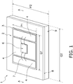
- FIG. 1 is a cross-sectional view of a semiconductor device 1 according to the embodiment.
- FIG. 2 is a cross-sectional view of A-A of FIG.
- the semiconductor device 1 is used as power module in various electronic devices such as an automobile, an air conditioner, an industrial robot, a commercial elevator, a household microwave oven, an IH electric rice cooker, power generation (wind power generation, solar power generation, fuel cell, or the like), electric railway, UPS (uninterruptible power supply) or the like.
- the semiconductor device 1 includes a semiconductor device substrate 2, a semiconductor chip 6, a bonding wire 7, a heat sink 8, and a heat radiating portion 9.
- the semiconductor device substrate 2 is a so-called DBOC substrate (Direct Bonding of Copper Substrate) or a DBOA substrate (Direct Bonding of Aluminum Substrate).
- DBOC substrate Direct Bonding of Copper Substrate
- DBOA substrate Direct Bonding of Aluminum Substrate
- the size and plane shape of the semiconductor device substrate 2 are not particularly limited but can be, for example, a square or rectangle having a vertical length P1 of 25 to 40 mm and a horizontal length Q1 of 35 to 50 mm.
- the thickness of each component constituting the semiconductor device substrate 2 will be described later.
- the semiconductor device substrate 2 includes a ceramic sintered body 3, a first circuit plate 4, and a second circuit plate 4'.
- the ceramic sintered body 3 is an insulator for the semiconductor device substrate 2.
- the ceramic sintered body 3 is formed in a flat plate shape.
- the ceramic sintered body 3 includes a first main surface F1 and a second main surface F2 on the opposite side of the first main surface. The constituent elements of the ceramic sintered body 3 will be described later.
- the first circuit plate 4 is arranged on the first main surface F1 of the ceramic sintered body 3.
- the first circuit plate 4 is constituted of copper or aluminum.
- the first circuit plate 4 is formed in a flat plate shape.
- the first circuit plate 4 is directly bonded to the first main surface F1 of the ceramic sintered body 3.
- the first circuit plate 4 according to the present embodiment is composed of three plate members, whereby a transmission circuit is formed.
- the plane shape of the first circuit plate 4 is not particularly limited, and a desired transmission circuit may be formed by a plurality of plate members.
- the coverage of the first main surface F1 by the first circuit plate 4 is not particularly limited but can be, for example, 85% or more and 95% or less.
- the coverage of the first main surface F1 by the first circuit plate 4 is obtained by dividing the total area of the first circuit plate 4 by the total area of the first main surface F1 in the plan view of the first main surface F1.
- the second circuit plate 4' is arranged on the second main surface F2 of the ceramic sintered body 3.
- the second circuit plate 4' is constituted of copper or aluminum.
- the second circuit plate 4' is formed in a flat plate shape.
- the second circuit plate 4' is directly bonded to the second main surface F2 of the ceramic sintered body 3.
- the second circuit plate 4' is a single plate member.
- the coverage of the second main surface F2 by the second circuit plate 4' is not particularly limited but can be, for example, 90% or more and 96% or less.
- the coverage of the second main surface F2 by the second circuit plate 4' is obtained by dividing the total area of the second circuit plate 4' by the total area of the second main surface F2 in the plan view of the semiconductor device substrate 2.
- the coverage of the second main surface F2 by the second circuit plate 4' may be the same as the coverage of the first main surface F1 by the first circuit plate 4 or may be larger than the coverage of the first main surface F1 by the first circuit plate 4.
- the total area of the second circuit plate 4' may be the same as the total area of the first circuit plate 4 or may be larger than the total area of the first circuit plate 4.
- the method for manufacturing the semiconductor device substrate 2 is not particularly limited, and for example, it can be manufactured as follows. First, a laminated body is formed in which the first circuit plate 4 is arranged on the first main surface F1 side of the ceramic sintered body 3 and the second circuit plate 4' is arranged on the second main surface F2 side of the ceramic sintered body 3. Next, the laminate is heated for about 10 minutes under nitrogen atmosphere conditions of 1070 degrees C to 1075 degrees C. As a result, a Cu-O eutectic liquid phase is generated at the interface where the ceramic sintered body 3 and the first and second circuit plates 4 and 4' are bonded (hereinafter, collectively referred to as "bonding interface"), and the first and second main surfaces F1 and F2 of the sintered body 3 get wet. Next, the Cu-O eutectic liquid phase is solidified by cooling the laminate, and the first and second copper plates 4 and 4' are bonded to the ceramic sintered body 3.
- the first copper plate 4 on which a transmission circuit is formed is bonded to the surface of the ceramic sintered body 3 in the semiconductor device substrate 2.
- the transmission circuit may be formed by a subtractive method or an additive method.
- the semiconductor chip 6 is bonded to the first circuit plate 4.
- the bonding wire 7 connects the semiconductor chip 6 and the first circuit plate 4.
- the heat sink 8 is bonded to the second circuit plate 4'.
- the heat sink 8 absorbs the heat of the semiconductor chip 6 transmitted via the semiconductor device substrate 2.
- the heat sink 8 can be constituted of, for example, copper or the like.
- the size and shape of the heat sink 8 are not particularly limited.
- the heat radiating portion 9 is attached to the heat sink 8.
- the heat radiating portion 9 radiates the heat of the semiconductor chip 6 transmitted via the semiconductor device substrate 2 and the heat sink 8 to the outside air.
- the heat radiating portion 9 can be constituted of, for example, aluminum or the like.
- the size and shape of the heat radiating portion 9 are not particularly limited.
- the heat radiating portion 9 preferably includes a plurality of fin portions 9a. As a result, it is possible to improve the heat radiating efficiency of the heat radiating portion 9.
- the plane size and plane shape of the heat sink 8 and the heat radiating portion 9 are not particularly limited but may be, for example, a square or rectangle having a vertical length P2 of 25 to 40 mm and a horizontal length Q2 of 35 to 50 mm.
- the ceramic sintered body 3 contains Al (aluminum), Zr (zirconium), Y (yttrium), and Mg (magnesium).
- the Al content in the ceramic sintered body 3 can be 75 mass% or more and 92.5 mass% or less in terms of Al 2 O 3 .
- the Al content in the ceramic sintered body 3 is preferably 75 mass% or more and 85 mass% or less in terms of Al 2 O 3 .
- the Zr content (described later, S2) in the ceramic sintered body 3 can be 5 % or more and 27.5 mass% or less in terms of ZrO 2 and is preferably 7.5 mass% or more and 25 mass% or less in terms of ZrO 2 and further preferably 17.5 mass% or more and 23.5 mass% or less in terms of ZrO 2 .
- the Y content in the ceramic sintered body 3 can be 0.3 mass% or more and 2.0 mass% or less in terms of Y 2 O 3 .
- the Y content in the ceramic sintered body 3 is preferably 0.7 mass% or more and 2.0 mass% or less in terms of Y 2 O 3 .
- the Mg content (S1 described later) in the ceramic sintered body 3 can be larger than 0.08 mass% and less than 1.18 mass% in terms of MgO.
- Mg content it is possible to prevent excessive growth of alumina and zirconia crystals and improve the mechanical strength of the ceramic sintered body 3. As a result, it is considered that it contributes to prevent cracks from occurring at the bonding interface. Further, it is considered that it is possible to prevent the excessive generation of MgAl 2 O 4 crystals in the ceramic sintered body 3 and prevent the excessive reaction at the bonding interface at the time of circuit plate bonding. As a result, it is considered that it contributes to prevent voids from generating at the bonding interface.
- the ceramic sintered body 3 may contain at least one of Hf (hafnium), Si (silicon), Ca (calcium), Na (sodium) and K (potassium), and the balance other than these.
- the element contained in the balance may be an element that is intentionally added or an element that is unavoidably mixed.
- the elements contained in the balance are not particularly limited, examples thereof include Fe (iron), Ti (titanium), Mn (manganese), or the like.
- the content of the constituent elements of the ceramic sintered body 3 is calculated in terms of oxide as described above, the constituent elements of the ceramic sintered body 3 may or may not exist in the form of oxide.
- the constituent elements of the ceramic sintered body 3 may or may not exist in the form of oxide.
- at least one of Y, Mg and Ca may not exist in the form of an oxide and may be dissolved in Zr02.
- the content of the constituent elements of the ceramic sintered body 3 in terms of oxide is calculated as follows. First, the constituent elements of the ceramic sintered body 3 are qualitatively analyzed using an energy dispersive analyzer (EDS) attached to a fluorescent X-ray analyzer (XRF) or a scanning electron microscope (SEM). Next, each element detected by this qualitative analysis is quantitatively analyzed using an ICP emission spectroscopic analyzer. Next, the content of each element measured by this quantitative analysis is converted into an oxide.
- EDS energy dispersive analyzer
- XRF fluorescent X-ray analyzer
- SEM scanning electron microscope
- the thickness T1 mm of the first circuit plate may be the same as the thickness T2 mm of the second circuit plate or may be larger than the thickness T2 mm of the second circuit plate.
- the ceramic sintered body 3 may be deformed concavely toward the second circuit plate 4' at the time of bonding the circuit plates. Therefore, when the total area of the second circuit plate 4' is larger than the total area of the first circuit plate 4, the thickness T1 mm of the first circuit plate is preferably larger than the thickness T2 mm of the second circuit plate.
- FIG. 2 is a flowchart showing a method for manufacturing the ceramic sintered body 3.
- step S1 in addition to Al 2 O 3 , ZrO 2 , Y 2 O 3 and MgO, powder materials such as HfO 2 , SiO 2 , CaO, Na 2 O, K 2 O or the like are prepared as desired.
- each of ZrO 2 and Y 2 O 3 may be a single powder material, a powder material of ZrO 2 partially stabilized by Y 2 O 3 may be used. Further, Mg, Ca, and alkali metals (Na and K) may be carbonate powders.
- step S2 the prepared powder material is pulverized and mixed by, for example, a ball mill.
- step S3 an organic binder (for example, polyvinyl butyral), a solvent (xylene, toluene, or the like) and a plasticizer (dioctyl phthalate) are added to the pulverized and mixed powder material to form a slurry-like substance.
- organic binder for example, polyvinyl butyral
- solvent xylene, toluene, or the like
- plasticizer dioctyl phthalate
- step S4 the slurry-like substance is molded into a desired shape by a desired molding means (for example, mold press, cold hydrostatic press, injection molding, doctor blade method, extrusion molding method, or the like) to form a ceramic molded product.
- a desired molding means for example, mold press, cold hydrostatic press, injection molding, doctor blade method, extrusion molding method, or the like.
- step S5 the ceramic molded product is fired in an oxygen atmosphere or an air atmosphere (at 150 degrees C to 1620 degrees C, 0.7 hours to 1.0 hours).
- the semiconductor device 1 including the configurations illustrated in FIGS. 1 and 2 was manufactured, and the thermal resistance of the semiconductor device 1 and the number of thermal cycles in which cracks were generated were measured.
- powder materials of Al 2 O 3 , ZrO 2 , Y 2 O 3 and MgO were prepared, and the powder materials were pulverized and mixed by a ball mill.
- the ZrO 2 content S2 and the MgO content S1 were changed for each sample as illustrated in Table 1, and the balance was regarded as Al 2 O 3 .
- polyvinyl butyral as an organic binder xylene as a solvent, and dioctyl phthalate as a plasticizer were added to the pulverized and mixed powder material to form a slurry-like substance.
- a ceramic molded body was produced by molding a slurry-like substance into a sheet by the doctor blade method. At this time, by changing the gate height of the blade, the thickness of the ceramic molded body was adjusted for each sample so that the thickness T3 of the ceramic sintered body 3 became the value illustrated in Table 1.
- the ceramic molded product was fired in an air atmosphere (at 1600 degrees C, to 0.8 hours) to prepare a ceramic sintered body 3.
- the vertical length P1 of the ceramic sintered body 3 was 40 mm, and the horizontal length Q1 was 40 mm.
- the first circuit plate 4 constituted of oxygen-free copper conforming to JIS C1020 one sheet having a vertical length of 37.4 mm x a horizontal length of 19.8 mm and two sheets having a vertical length of 37.4 mm x a horizontal length of 7.8 mm
- the second circuit plate 4' one sheet having a vertical length of 37.4 mm and a horizontal length of 37.4 mm
- the thickness T1 of the first circuit plate 4 and the thickness T2 of the second circuit plate 4' were different for each sample as illustrated in Table 1.
- the outer surfaces of the first and second circuit plates 4 and 4' were oxidized by heating to 300 degrees C in the atmosphere.
- the laminate in which the ceramic sintered body 3 was sandwiched between the first and second circuit plates 4, 4' was heated at 1070 degrees C for 10 minutes in the nitrogen (N 2 ) atmosphere.
- the first and second circuit plates 4, 4' were bonded to the ceramic sintered body 3 by cooling the laminate.
- the coverage of the first main surface F1 by the first circuit plate 4 was 82.7%, and the coverage of the second main surface F2 by the second circuit plate 4' was 87.4%.
- a copper heat sink 8 (length 60 mm x width 60 mm x thickness 3 mm) to which an aluminum heat sink 9 (length 60 mm x width 60 mm x thickness 6.5 mm) is attached was bonded to the second circuit plate 4'.
- the Si semiconductor chip 6 is bonded to the first circuit plate 4, and also the bonding wire 7 was attached to the Si semiconductor chip 6 (length 10 mm ⁇ width 10 mm ⁇ thickness 0.35 mm) and the first circuit plate 4.
- the thermal resistance R J-a (degrees C/W) of the semiconductor device 1 was measured from the following formula (8) by energizing the Si semiconductor chip 6 and generating heat.
- T j is the element temperature (degrees C) of the Si semiconductor chip 6
- Ta is the ambient temperature (degrees C) of the Si semiconductor chip 6
- Q is the electric power (W) supplied to the Si semiconductor chip 6.
- R J ⁇ a T j ⁇ T a / Q
- the relative thickness with respect to the ceramic sintered body 3 having a low thermal conductivity and the first and second circuit plates 4 and 4' having a high thermal conductivity was not optimized, so that the thermal conductivity of the semiconductor device substrate 2 as a whole was high.
- the semiconductor device substrate according to the present invention can be used in various electronic devices.
Landscapes
- Chemical & Material Sciences (AREA)
- Engineering & Computer Science (AREA)
- Ceramic Engineering (AREA)
- Materials Engineering (AREA)
- Structural Engineering (AREA)
- Organic Chemistry (AREA)
- Microelectronics & Electronic Packaging (AREA)
- Inorganic Chemistry (AREA)
- Manufacturing & Machinery (AREA)
- Composite Materials (AREA)
- Cooling Or The Like Of Semiconductors Or Solid State Devices (AREA)
- Compositions Of Oxide Ceramics (AREA)
Abstract
Description
- The present invention relates to a substrate for a semiconductor device.
- As a substrate for a semiconductor device used for a power transistor module or the like, a DBOC substrate (Direct Bonding of Copper Substrate) including a copper plate on the surface of a ceramic sintered body or a DBOA substrate (Direct Bonding of Aluminum Substrate) including an aluminum plate on the surface of a ceramic sintered body is known.
-
PATENT LITERATURE 1 discloses a substrate for a semiconductor device including a ceramic sintered body containing alumina, partially stabilized zirconia, and magnesia. In the ceramic sintered body described inPATENT LITERATURE 1, the content of partially stabilized zirconia is 1 to 30 wt%, and the content of magnesia is 0.05 to 0.50 wt%. The molar fraction of yttria in partially stabilized zirconia is 0.015 to 0.035, and 80 to 100% of the zirconia crystals contained in the ceramic sintered body are tetragonal phases. The ceramic sintered body described in PATENTLITERATURE 1 is supposed to be capable of preventing cracks from occurring at the bonding interface between the ceramic sintered body and the circuit plate or the aluminum plate and improving the thermal conductivity. -
PATENT LITERATURE 2 discloses a substrate for a semiconductor device including a ceramic sintered body containing alumina, zirconia, and yttria. In the ceramic sintered body described inPATENT LITERATURE 2, the content of zirconia is 2 to 15 wt%, and the average particle size of alumina is 2 to 8 µm. The ceramic sintered body described in PATENTLITERATURE 2 is supposed to be capable of improving the thermal conductivity. -
- [Patent Literature 1]
JP 4717960B - [Patent Literature 2]
JP 2015-534280A - However, in
PATENT LITERATURE 1, although the thermal conductivity of the ceramic sintered body itself is examined, the thermal resistance of the semiconductor device substrate as a whole including the circuit plate (circuit plate or aluminum plate) has not been examined. - Similarly, in PATENT
LITERATURE 2, the thermal resistance of the semiconductor device substrate as a whole is not examined, and cracks at the bonding interface are not examined either. - Therefore, as a result of diligent studies by the present inventor, a new finding that the combination of the composition of the ceramic sintered body and the thickness of each constituent member affects the thermal resistance of the substrate for semiconductor device and the cracks at the bonding interface has been obtained.
- An object of the present invention is to provide a substrate for a semiconductor device capable of achieving both to reduce thermal resistance and prevent cracks.
- The substrate for a semiconductor device according to the present invention includes a ceramic sintered body, a first circuit plate, and a second circuit plate. The ceramic sintered body is formed in a plate shape and has a first main surface and a second main surface. The first circuit plate is arranged on the first main surface and is constituted of copper or aluminum. The second circuit plate is arranged on the second main surface and is constituted of copper or aluminum. The ceramic sintered body contains Al, Zr, Y and Mg. In the ceramic sintered body, when the Mg content in terms of MgO is S1 mass% and the Zr content in terms of ZrO2 is S2 mass%, the following formula (1) is established. When the thickness of the first circuit plate is T1 mm, the thickness of the second circuit plate is T2 mm, and the thickness of the ceramic sintered body is T3 mm, the following formulas (2), (3), and (4) are established.




- According to the present invention, it is possible to provide a substrate for a semiconductor device capable of achieving both to reduce thermal resistance and prevent cracks.
-
-
FIG. 1 is a perspective view showing a configuration of a semiconductor device according to an embodiment. -
FIG. 2 is a cross-sectional view of A-A inFIG. 1 . -
FIG. 3 is a flowchart for explaining a method of manufacturing a substrate for a semiconductor device according to an embodiment. - Hereinafter, the configuration of the semiconductor device according to the present invention will be described with reference to the drawings.
-
FIG. 1 is a cross-sectional view of asemiconductor device 1 according to the embodiment.FIG. 2 is a cross-sectional view of A-A of FIG. - The
semiconductor device 1 is used as power module in various electronic devices such as an automobile, an air conditioner, an industrial robot, a commercial elevator, a household microwave oven, an IH electric rice cooker, power generation (wind power generation, solar power generation, fuel cell, or the like), electric railway, UPS (uninterruptible power supply) or the like. - The
semiconductor device 1 includes asemiconductor device substrate 2, asemiconductor chip 6, abonding wire 7, aheat sink 8, and aheat radiating portion 9. - The
semiconductor device substrate 2 is a so-called DBOC substrate (Direct Bonding of Copper Substrate) or a DBOA substrate (Direct Bonding of Aluminum Substrate). - The size and plane shape of the
semiconductor device substrate 2 are not particularly limited but can be, for example, a square or rectangle having a vertical length P1 of 25 to 40 mm and a horizontal length Q1 of 35 to 50 mm. The thickness of each component constituting thesemiconductor device substrate 2 will be described later. - The
semiconductor device substrate 2 includes a ceramicsintered body 3, afirst circuit plate 4, and a second circuit plate 4'. - The ceramic sintered
body 3 is an insulator for thesemiconductor device substrate 2. The ceramic sinteredbody 3 is formed in a flat plate shape. The ceramic sinteredbody 3 includes a first main surface F1 and a second main surface F2 on the opposite side of the first main surface. The constituent elements of the ceramic sinteredbody 3 will be described later. - The
first circuit plate 4 is arranged on the first main surface F1 of the ceramic sinteredbody 3. Thefirst circuit plate 4 is constituted of copper or aluminum. Thefirst circuit plate 4 is formed in a flat plate shape. Thefirst circuit plate 4 is directly bonded to the first main surface F1 of the ceramic sinteredbody 3. Thefirst circuit plate 4 according to the present embodiment is composed of three plate members, whereby a transmission circuit is formed. However, the plane shape of thefirst circuit plate 4 is not particularly limited, and a desired transmission circuit may be formed by a plurality of plate members. - The coverage of the first main surface F1 by the
first circuit plate 4 is not particularly limited but can be, for example, 85% or more and 95% or less. The coverage of the first main surface F1 by thefirst circuit plate 4 is obtained by dividing the total area of thefirst circuit plate 4 by the total area of the first main surface F1 in the plan view of the first main surface F1. - The second circuit plate 4' is arranged on the second main surface F2 of the ceramic sintered
body 3. The second circuit plate 4' is constituted of copper or aluminum. The second circuit plate 4' is formed in a flat plate shape. The second circuit plate 4' is directly bonded to the second main surface F2 of the ceramic sinteredbody 3. The second circuit plate 4' is a single plate member. - The coverage of the second main surface F2 by the second circuit plate 4' is not particularly limited but can be, for example, 90% or more and 96% or less. The coverage of the second main surface F2 by the second circuit plate 4' is obtained by dividing the total area of the second circuit plate 4' by the total area of the second main surface F2 in the plan view of the
semiconductor device substrate 2. The coverage of the second main surface F2 by the second circuit plate 4' may be the same as the coverage of the first main surface F1 by thefirst circuit plate 4 or may be larger than the coverage of the first main surface F1 by thefirst circuit plate 4. The total area of the second circuit plate 4' may be the same as the total area of thefirst circuit plate 4 or may be larger than the total area of thefirst circuit plate 4. - The method for manufacturing the
semiconductor device substrate 2 is not particularly limited, and for example, it can be manufactured as follows. First, a laminated body is formed in which thefirst circuit plate 4 is arranged on the first main surface F1 side of the ceramicsintered body 3 and the second circuit plate 4' is arranged on the second main surface F2 side of the ceramicsintered body 3. Next, the laminate is heated for about 10 minutes under nitrogen atmosphere conditions of 1070 degrees C to 1075 degrees C. As a result, a Cu-O eutectic liquid phase is generated at the interface where the ceramicsintered body 3 and the first andsecond circuit plates 4 and 4' are bonded (hereinafter, collectively referred to as "bonding interface"), and the first and second main surfaces F1 and F2 of thesintered body 3 get wet. Next, the Cu-O eutectic liquid phase is solidified by cooling the laminate, and the first andsecond copper plates 4 and 4' are bonded to the ceramicsintered body 3. - The
first copper plate 4 on which a transmission circuit is formed is bonded to the surface of the ceramicsintered body 3 in thesemiconductor device substrate 2. The transmission circuit may be formed by a subtractive method or an additive method. - The
semiconductor chip 6 is bonded to thefirst circuit plate 4. Thebonding wire 7 connects thesemiconductor chip 6 and thefirst circuit plate 4. - The
heat sink 8 is bonded to the second circuit plate 4'. Theheat sink 8 absorbs the heat of thesemiconductor chip 6 transmitted via thesemiconductor device substrate 2. Theheat sink 8 can be constituted of, for example, copper or the like. The size and shape of theheat sink 8 are not particularly limited. - The
heat radiating portion 9 is attached to theheat sink 8. Theheat radiating portion 9 radiates the heat of thesemiconductor chip 6 transmitted via thesemiconductor device substrate 2 and theheat sink 8 to the outside air. Theheat radiating portion 9 can be constituted of, for example, aluminum or the like. The size and shape of theheat radiating portion 9 are not particularly limited. Theheat radiating portion 9 preferably includes a plurality offin portions 9a. As a result, it is possible to improve the heat radiating efficiency of theheat radiating portion 9. - The plane size and plane shape of the
heat sink 8 and theheat radiating portion 9 are not particularly limited but may be, for example, a square or rectangle having a vertical length P2 of 25 to 40 mm and a horizontal length Q2 of 35 to 50 mm. - The ceramic
sintered body 3 contains Al (aluminum), Zr (zirconium), Y (yttrium), and Mg (magnesium). - The Al content in the ceramic
sintered body 3 can be 75 mass% or more and 92.5 mass% or less in terms of Al2O3. The Al content in the ceramicsintered body 3 is preferably 75 mass% or more and 85 mass% or less in terms of Al2O3. - The Zr content (described later, S2) in the ceramic
sintered body 3 can be 5 % or more and 27.5 mass% or less in terms of ZrO2 and is preferably 7.5 mass% or more and 25 mass% or less in terms of ZrO2 and further preferably 17.5 mass% or more and 23.5 mass% or less in terms of ZrO2. - It is considered that by setting the Zr content to 7.5 mass% or more in terms of ZrO2, it is possible to prevent the linear thermal expansion coefficient α of the ceramic
sintered body 3 from becoming too small, and it is possible to reduce the difference in the linear thermal expansion coefficient of the ceramicsintered body 3 and the first andsecond circuit plates 4 and 4'. As a result, it is considered that it contributes to prevent cracks from occurring at the bonding interface. This effect can be further improved by setting the Zr content to 17.5 mass% or more in terms of ZrO2. - It is considered that by setting the Zr content to 25 mass% or less in terms of ZrO2, it is possible to prevent an excessive reaction at the bonding interface at the time of circuit plate bonding, and it is possible to prevent voids from forming at the bonding interface. As a result, it is considered that it contributes to prevent cracks at the bonding interface. This effect can be further improved by setting the Zr content to 23.5 mass% or less in terms of ZrO2.
- The Y content in the ceramic
sintered body 3 can be 0.3 mass% or more and 2.0 mass% or less in terms of Y2O3. The Y content in the ceramicsintered body 3 is preferably 0.7 mass% or more and 2.0 mass% or less in terms of Y2O3. - It is considered that by setting the Y content to 0.3 mass% or more in terms of Y2O3, it is possible to prevent the peak intensity ratio of the monoclinic crystal phase from being excessive among the ZrO2 crystal phases contained in the ceramic
sintered body 3 as the crystal phase. As a result, it is considered that the mechanical strength of the ceramicsintered body 3 can be improved, so that it contributes to prevent cracks from occurring at the bonding interface. - It is considered that by setting the Y content to 2.0 mass% or less in terms of Y2O3, it is possible to prevent the peak intensity ratio of the monoclinic crystal phase from being too small among the ZrO2 crystal phases contained in the ceramic
sintered body 3 as the crystal phase. As a result, it is considered that the mechanical strength of the ceramicsintered body 3 can be improved, so that it contributes to prevent cracks from occurring at the bonding interface. - The Mg content (S1 described later) in the ceramic
sintered body 3 can be larger than 0.08 mass% and less than 1.18 mass% in terms of MgO. - It is considered that by increasing the Mg content to more than 0.08 mass% in terms of MgO, it is possible to sinter the ceramic
sintered body 3 without excessively raising the firing temperature, and it is possible to prevent Al2O3 particles and ZrO2 particles from coarsening. As a result, it is considered that the mechanical strength of the ceramicsintered body 3 can be improved, so that contributes to prevent cracks from occurring at the bonding interface. Further, it is considered that it is possible to generate a sufficient amount of MgAl2O4 (spinel) crystals in the ceramicsintered body 3, and it is possible to improve the wettability with the Cu-O eutectic liquid phase at the time of bonding the circuit plate. As a result, it is considered that it contributes to prevent voids from occurring at the bonding interface. - It is considered that by setting the Mg content to less than 1.18 mass% in terms of MgO, it is possible to prevent excessive growth of alumina and zirconia crystals and improve the mechanical strength of the ceramic
sintered body 3. As a result, it is considered that it contributes to prevent cracks from occurring at the bonding interface. Further, it is considered that it is possible to prevent the excessive generation of MgAl2O4 crystals in the ceramicsintered body 3 and prevent the excessive reaction at the bonding interface at the time of circuit plate bonding. As a result, it is considered that it contributes to prevent voids from generating at the bonding interface. - The ceramic
sintered body 3 may contain at least one of Hf (hafnium), Si (silicon), Ca (calcium), Na (sodium) and K (potassium), and the balance other than these. The element contained in the balance may be an element that is intentionally added or an element that is unavoidably mixed. Although the elements contained in the balance are not particularly limited, examples thereof include Fe (iron), Ti (titanium), Mn (manganese), or the like. - Although in the present embodiment, the content of the constituent elements of the ceramic
sintered body 3 is calculated in terms of oxide as described above, the constituent elements of the ceramicsintered body 3 may or may not exist in the form of oxide. For example, at least one of Y, Mg and Ca may not exist in the form of an oxide and may be dissolved in Zr02. - Note that the content of the constituent elements of the ceramic
sintered body 3 in terms of oxide is calculated as follows. First, the constituent elements of the ceramicsintered body 3 are qualitatively analyzed using an energy dispersive analyzer (EDS) attached to a fluorescent X-ray analyzer (XRF) or a scanning electron microscope (SEM). Next, each element detected by this qualitative analysis is quantitatively analyzed using an ICP emission spectroscopic analyzer. Next, the content of each element measured by this quantitative analysis is converted into an oxide. - (Composition of ceramic
sintered body 3 and thickness of each component) - Next, the combination of the composition of the ceramic
sintered body 3 and the thicknesses of the ceramicsintered body 3, thefirst circuit plate 4 and the second circuit plate 4'will be described. - When the Mg content in the ceramic
sintered body 3 in terms of MgO is S1 mass% and the Zr content in terms of ZrO2 is S2 mass%, the following formula (1) is established.
- When the thickness of the first circuit plate is T1 mm, the thickness of the second circuit plate is T2 mm, and the thickness of the ceramic sintered body is T3 mm, the following formulas (2), (3), (4) are established.


- By establishing the above formulas (1) to (4), it is possible to prevent cracks from occurring at the bonding interface even if the ceramic
sintered body 3 is subjected to a thermal cycle and also decrease the heat resistance rate of thesemiconductor device substrate 2 as a whole. Although the mechanism by which such an effect is obtained is not always clear, it is considered to be a synergistic effect of that the mechanical strength of the ceramicsintered body 3 is increased by satisfying upper limit value of the formulas (1) and (2) and the formula (4) and that the optimization of the relative thickness of the ceramicsintered body 3 having a low thermal conductivity and the first andsecond circuit plates 4 and 4' having a high thermal conductivity by satisfying the lower limit value of the formula (2) and the formula (3). - As illustrated in the formula (3), the thickness T1 mm of the first circuit plate may be the same as the thickness T2 mm of the second circuit plate or may be larger than the thickness T2 mm of the second circuit plate. However, if the total area of the second circuit plate 4' is larger than the total area of the
first circuit plate 4, the ceramicsintered body 3 may be deformed concavely toward the second circuit plate 4' at the time of bonding the circuit plates. Therefore, when the total area of the second circuit plate 4' is larger than the total area of thefirst circuit plate 4, the thickness T1 mm of the first circuit plate is preferably larger than the thickness T2 mm of the second circuit plate. - Regarding the content S2 of Zr in the ceramic
sintered body 3 in terms of ZrO2, it is preferable that the following formula (5) is established.
- By establishing the formula (5), as described above, it is possible to further increase the mechanical strength of the ceramic sintered body, so that it is possible to further prevent cracks from occurring at the bonding interface.
- Regarding the Zr content S2 in the ceramic
sintered body 3 in terms of ZrO2, it is more preferable that the following formula (6) is established.
- By establishing the formula (6), it is possible to further increase the mechanical strength of the ceramic
sintered body 3, so that it is possible to prevent cracks from occurring at the bonding interface. - Regarding the Mg content S1 in the ceramic
sintered body 3 in terms of MgO, it is more preferable that the following formula (7) is established.
- By establishing the formula (7), as described above, it is possible to further increase the mechanical strength of the ceramic
sintered body 3, so that it is possible to prevent cracks from occurring at the bonding interface. - With reference to
FIG. 2 , a method for manufacturing the ceramicsintered body 3 will be described.FIG. 2 is a flowchart showing a method for manufacturing the ceramicsintered body 3. - In step S1, in addition to Al2O3, ZrO2, Y2O3 and MgO, powder materials such as HfO2, SiO2, CaO, Na2O, K2O or the like are prepared as desired.
- Note that although each of ZrO2 and Y2O3 may be a single powder material, a powder material of ZrO2 partially stabilized by Y2O3 may be used. Further, Mg, Ca, and alkali metals (Na and K) may be carbonate powders.
- In step S2, the prepared powder material is pulverized and mixed by, for example, a ball mill.
- In step S3, an organic binder (for example, polyvinyl butyral), a solvent (xylene, toluene, or the like) and a plasticizer (dioctyl phthalate) are added to the pulverized and mixed powder material to form a slurry-like substance.
- In step S4, the slurry-like substance is molded into a desired shape by a desired molding means (for example, mold press, cold hydrostatic press, injection molding, doctor blade method, extrusion molding method, or the like) to form a ceramic molded product. At this time, in order to establish the above formulas (2) to (4) regarding the thickness T3 of the ceramic
sintered body 3 in relation to the thickness T1 of the first circuit plate and the thickness T2 of the second circuit plate, the thickness of the ceramic molded body is adjusted in consideration of the firing shrinkage rate in step S5. - In step S5, the ceramic molded product is fired in an oxygen atmosphere or an air atmosphere (at 150 degrees C to 1620 degrees C, 0.7 hours to 1.0 hours).
- As Sample Nos. 1 to 72, the
semiconductor device 1 including the configurations illustrated inFIGS. 1 and2 was manufactured, and the thermal resistance of thesemiconductor device 1 and the number of thermal cycles in which cracks were generated were measured. - First, powder materials of Al2O3, ZrO2, Y2O3 and MgO were prepared, and the powder materials were pulverized and mixed by a ball mill. At this time, the ZrO2 content S2 and the MgO content S1 were changed for each sample as illustrated in Table 1, and the balance was regarded as Al2O3.
- Next, polyvinyl butyral as an organic binder, xylene as a solvent, and dioctyl phthalate as a plasticizer were added to the pulverized and mixed powder material to form a slurry-like substance.
- Next, a ceramic molded body was produced by molding a slurry-like substance into a sheet by the doctor blade method. At this time, by changing the gate height of the blade, the thickness of the ceramic molded body was adjusted for each sample so that the thickness T3 of the ceramic
sintered body 3 became the value illustrated in Table 1. - Next, the ceramic molded product was fired in an air atmosphere (at 1600 degrees C, to 0.8 hours) to prepare a ceramic
sintered body 3. The vertical length P1 of the ceramicsintered body 3 was 40 mm, and the horizontal length Q1 was 40 mm. - Next, the
first circuit plate 4 constituted of oxygen-free copper conforming to JIS C1020 (one sheet having a vertical length of 37.4 mm x a horizontal length of 19.8 mm and two sheets having a vertical length of 37.4 mm x a horizontal length of 7.8 mm) and the second circuit plate 4' (one sheet having a vertical length of 37.4 mm and a horizontal length of 37.4 mm) were prepared. The thickness T1 of thefirst circuit plate 4 and the thickness T2 of the second circuit plate 4' were different for each sample as illustrated in Table 1. - Next, the outer surfaces of the first and
second circuit plates 4 and 4'were oxidized by heating to 300 degrees C in the atmosphere. - Next, the laminate in which the ceramic
sintered body 3 was sandwiched between the first andsecond circuit plates 4, 4' was heated at 1070 degrees C for 10 minutes in the nitrogen (N2) atmosphere. - Next, the first and
second circuit plates 4, 4' were bonded to the ceramicsintered body 3 by cooling the laminate. The coverage of the first main surface F1 by thefirst circuit plate 4 was 82.7%, and the coverage of the second main surface F2 by the second circuit plate 4' was 87.4%. - Next, by using solder, a copper heat sink 8 (length 60 mm x width 60 mm x
thickness 3 mm) to which an aluminum heat sink 9 (length 60 mm x width 60 mm x thickness 6.5 mm) is attached was bonded to the second circuit plate 4'. - Next, by using solder, the
Si semiconductor chip 6 is bonded to thefirst circuit plate 4, and also thebonding wire 7 was attached to the Si semiconductor chip 6 (length 10 mm × width 10 mm × thickness 0.35 mm) and thefirst circuit plate 4. - Regarding sample Nos. 1 to 72, the thermal resistance RJ-a (degrees C/W) of the
semiconductor device 1 was measured from the following formula (8) by energizing theSi semiconductor chip 6 and generating heat. However, in the formula (8), Tj is the element temperature (degrees C) of theSi semiconductor chip 6, Ta is the ambient temperature (degrees C) of theSi semiconductor chip 6, and Q is the electric power (W) supplied to theSi semiconductor chip 6.
- In Table 1, regarding each of sample Nos. 1 to 72, the average value of the thermal resistance of 10 pieces is described. In Table 1, samples having a thermal resistance (degrees C/W) of 0.805 or more is evaluated as "x", and samples having a thermal resistance of 0.790 or more and 0.805 or less is evaluated as "Δ", and samples having a thermal resistance of 0.790 or less is evaluated as "○".
- Regarding sample Nos. 1 to 72, the cycle of "first at -40 degrees C for 30 minutes, secondly at 25 degrees C for 5 minutes, thirdly at 125 degrees C for 30 minutes, and finally at 25 degrees C for 5 minutes" was repeated until cracks occurred in the ceramic
sintered body 3. - In Table 1, regarding each of sample Nos. 1 to 72, the number of cycles in which cracks occur in any of the 10 pieces is described as the number of crack generation cycles. In Table 1, samples having 51 or more crack generation cycles (times) are evaluated as "○", samples having 31 or more and 50 or less are evaluated as "Δ", and samples having 30 or less are evaluated as "x".
[Table 1] Sample Ceramic sintered body composition Range of formula (1) Substrate for semiconductor device Characterization Evaluated results S1:MgO S2:ZrO2 -0.004×S2+0.171 -0.032×S2+1.427 T1 T2 T3 (T1+T2)/T3 Thermal resistance (degrees C/W) Number of crack generation cycles (mass%) (mass%) (mass%) (mass%) (mm) (mm) (mm) No.1 0.52 5 0.15 1.27 0.30 0.30 0.25 2.40 0.768 ○ 35 Δ Δ No.2 0.13 7.5 0.14 1.19 0.30 0.30 0.25 2.40 0.770 ○ 25 × × No.3 0.16 7.5 0.14 1.19 0.30 0.30 0.25 2.40 0.770 ○ 35 Δ Δ No.4 1.17 7.5 0.14 1.19 0.30 0.30 0.25 2.40 0.770 ○ 40 Δ Δ No.5 1.20 7.5 0.14 1.19 0.30 0.30 0.25 2.40 0.770 ○ 30 × × No.6 0.53 7.5 0.14 1.19 0.20 0.20 0.32 1.25 0.806 × 40 Δ × No.7 0.53 7.5 0.14 1.19 0.30 0.30 0.32 1.88 0.787 ○ 35 Δ Δ No.8 0.53 7.5 0.14 1.19 0.30 0.30 0.25 2.40 0.770 ○ 55 O O No.9 0.53 7.5 0.14 1.19 0.50 0.50 0.32 3.13 0.763 ○ 40 Δ Δ No.10 0.53 7.5 0.14 1.19 0.60 0.60 0.32 3.75 0.753 ○ 30 × × No.11 0.53 7.5 0.14 1.19 0.10 0.10 0.20 1.00 0.813 × 35 Δ × No.12 0.12 10 0.13 1.11 0.30 0.30 0.25 2.40 0.772 ○ 30 × × No.13 0.15 10 0.13 1.11 0.30 0.30 0.25 2.40 0.772 ○ 35 Δ Δ No.14 1.09 10 0.13 1.11 0.30 0.30 0.25 2.40 0.772 ○ 40 Δ Δ No.15 1.12 10 0.13 1.11 0.30 0.30 0.25 2.40 0.772 ○ 30 × × No.16 0.50 10 0.13 1.11 0.20 0.20 0.32 1.25 0.809 × 45 Δ × No.17 0.50 10 0.13 1.11 0.30 0.30 0.32 1.88 0.790 Δ 50 Δ Δ No.18 0.50 10 0.13 1.11 0.30 0.30 0.25 2.40 0.772 ○ 55 ○ O No.19 0.50 10 0.13 1.11 0.50 0.50 0.32 3.13 0.765 ○ 40 Δ Δ No.20 0.50 10 0.13 1.11 0.60 0.60 0.32 3.75 0.755 ○ 30 × × No.21 0.50 10 0.13 1.11 0.10 0.10 0.20 1.00 0.817 × 40 Δ × No.22 0.10 15 0.11 0.95 0.30 0.30 0.25 2.40 0.777 ○ 30 × × No.23 0.13 15 0.11 0.95 0.30 0.30 0.25 2.40 0.777 ○ 60 ○ O No.24 0.93 15 0.11 0.95 0.30 0.30 0.25 2.40 0.777 ○ 70 ○ O No.25 0.96 15 0.11 0.95 0.30 0.30 0.25 2.40 0.777 ○ 25 × × No.26 0.42 15 0.11 0.95 0.20 0.20 0.32 1.25 0.813 × 80 ○ × No.27 0.42 15 0.11 0.95 0.30 0.30 0.32 1.88 0.796 Δ 70 ○ O No.28 0.42 15 0.11 0.95 0.30 0.30 0.25 2.40 0.777 ○ 60 ○ O No.29 0.42 15 0.11 0.95 0.50 0.50 0.32 3.13 0.770 ○ 55 O O No.30 0.42 15 0.11 0.95 0.60 0.60 0.32 3.75 0.760 ○ 30 × × No.31 0.42 15 0.11 0.95 0.10 0.10 0.20 1.00 0.825 × 55 ○ × No.32 0.09 17.5 0.10 0.87 0.30 0.30 0.25 2.40 0.780 ○ 30 × × No.33 0.12 17.5 0.10 0.87 0.30 0.30 0.25 2.40 0.780 ○ 125 ⊚ ⊚ No.34 0.85 17.5 0.10 0.87 0.30 0.30 0.25 2.40 0.780 ○ 150 ⊚ ⊚ No.35 0.88 17.5 0.10 0.87 0.30 0.30 0.25 2.40 0.780 ○ 30 × × No.36 0.39 17.5 0.10 0.87 0.20 0.20 0.32 1.25 0.815 × 90 ○ × No.37 0.39 17.5 0.10 0.87 0.30 0.30 0.32 1.88 0.798 Δ 125 ⊚ ⊚ No.38 0.39 17.5 0.10 0.87 0.30 0.30 0.25 2.40 0.780 ○ 125 ⊚ ⊚ No.39 0.39 17.5 0.10 0.87 0.50 0.50 0.32 3.13 0.773 ○ 125 ⊚ ⊚ No.40 0.39 17.5 0.10 0.87 0.60 0.60 0.32 3.75 0.762 ○ 30 × ⊚ No.41 0.50 17.5 0.10 0.87 0.10 0.10 0.20 1.00 0.828 × 100 ○ × No.42 0.08 20 0.09 0.79 0.30 0.30 0.25 2.40 0.784 ○ 25 × × No.43 0.11 20 0.09 0.79 0.30 0.30 0.25 2.40 0.784 ○ 175 ⊚ ⊚ No.44 0.77 20 0.09 0.79 0.30 0.30 0.25 2.40 0.784 ○ 150 ⊚ ⊚ No.45 0.80 20 0.09 0.79 0.30 0.30 0.25 2.40 0.784 ○ 30 × × No.46 0.35 20 0.09 0.79 0.20 0.20 0.32 1.25 0.820 × 125 ⊚ × No.47 0.35 20 0.09 0.79 0.30 0.30 0.32 1.88 0.800 Δ 125 ⊚ ⊚ No.48 0.35 20 0.09 0.79 0.30 0.30 0.25 2.40 0.784 ○ 175 ⊚ ⊚ No.49 0.35 20 0.09 0.79 0.50 0.50 0.32 3.13 0.777 ○ 125 ⊚ ⊚ No.50 0.35 20 0.09 0.79 0.60 0.60 0.32 3.75 0.766 ○ 30 × × No.51 0.35 20 0.09 0.79 0.10 0.10 0.20 1.00 0.832 × 125 ⊚ × No.52 0.07 23.5 0.08 0.68 0.30 0.30 0.25 2.40 0.787 ○ 30 × × No.53 0.10 23.5 0.08 0.68 0.30 0.30 0.25 2.40 0.787 ○ 150 ⊚ ⊚ No.54 0.66 23.5 0.08 0.68 0.30 0.30 0.25 2.40 0.787 ○ 150 ⊚ ⊚ No.55 0.69 23.5 0.08 0.68 0.30 0.30 0.25 2.40 0.787 ○ 30 × × No.56 0.30 23.5 0.08 0.68 0.20 0.20 0.32 1.25 0.823 × 100 ○ × No.57 0.30 23.5 0.08 0.68 0.30 0.30 0.32 1.88 0.802 Δ 125 ⊚ ⊚ No.58 0.30 23.5 0.08 0.68 0.30 0.30 0.25 2.40 0.787 ○ 150 ⊚ ⊚ No.59 0.30 23.5 0.08 0.68 0.50 0.50 0.32 3.13 0.780 ○ 125 ⊚ ⊚ No.60 0.30 23.5 0.08 0.68 0.60 0.60 0.32 3.75 0.768 ○ 25 × × No.61 0.50 23.5 0.08 0.68 0.10 0.10 0.20 1.00 0.835 × 80 ○ × No.62 0.06 25 0.07 0.63 0.30 0.30 0.25 2.40 0.791 Δ 30 × × No.63 0.09 25 0.07 0.63 0.30 0.30 0.25 2.40 0.791 Δ 60 ○ ○ No.64 0.61 25 0.07 0.63 0.30 0.30 0.25 2.40 0.791 Δ 70 ○ ○ No.65 0.64 25 0.07 0.63 0.30 0.30 0.25 2.40 0.791 Δ 30 × × No.66 0.28 25 0.07 0.63 0.20 0.20 0.32 1.25 0.827 × 55 ○ × No.67 0.28 25 0.07 0.63 0.30 0.30 0.32 1.88 0.804 Δ 60 ○ ○ No.68 0.28 25 0.07 0.63 0.30 0.30 0.25 2.40 0.791 Δ 80 ○ ○ No.69 0.28 25 0.07 0.63 0.50 0.50 0.32 3.13 0.784 ○ 55 O ○ No.70 0.28 25 0.07 0.63 0.60 0.60 0.32 3.75 0.772 ○ 25 × × No.71 0.28 25 0.07 0.63 0.10 0.10 0.20 1.00 0.842 × 60 ○ × No.72 0.22 27.5 0.06 0.55 0.30 0.30 0.25 2.40 0.795 Δ 35 Δ Δ - As illustrated in Table 1, in the samples in which all of the above formulas (1) to (4) were established, it was possible to prevent cracks from occurring at the bonding interface even if the ceramic
sintered body 3 was subjected to a thermal cycle, and also the thermal resistivity of thesemiconductor device substrate 2 as a whole could be reduced. - On the other hand, at the sample Nos. 2, 5, 12, 15, 22, 25, 32, 35, 42, 45, 52, 55, 62, and 65 which do not satisfy the formula (1), the mechanical strength of the ceramic
sintered body 3 was not sufficient, so that cracks were likely to occur at the bonding interface. Further, at the sample Nos. 10, 20, 30, 40, 50, 60, and 70 which do not satisfy upper limit value of the formula (2), the mechanical strength of the ceramicsintered body 3 was not sufficient, so that cracks were likely to occur at the bonding interface. In addition, at the sample Nos. 6, 11, 16, 21, 26, 31, 36, 41, 46, 51, 56, 61, 77, and 71 which do not satisfy the lower limit of the formula (2), the relative thickness with respect to the ceramicsintered body 3 having a low thermal conductivity and the first andsecond circuit plates 4 and 4' having a high thermal conductivity was not optimized, so that the thermal conductivity of thesemiconductor device substrate 2 as a whole was high. - In addition, according to comparing sample No.1 and sample Nos. 8 and 18, in the sample in which the above-mentioned formula (5) is established, it was possible to further prevent cracks from occurring at the bonding interface between the ceramic
sintered body 3 and the first andsecond circuit plates 4, 4'. - Further, in the sample in which the above-mentioned formula (6) is established, it was possible to further prevent cracks from occurring at the bonding interface between the ceramic
sintered body 3 and the first andsecond circuit plates 4, 4'. Note that this effect could be particularly improved in the samples in which the content of Zr in terms of ZrO2 was 17.5 mass% or more and 23.5 mass% or less. - According to the present invention, it is possible to both reduce the thermal resistance of the semiconductor device substrate and prevent cracks at the same time. Therefore, the semiconductor device substrate according to the present invention can be used in various electronic devices.
-
- 1 ...
- Semiconductor device
- 2 ...
- Substrate for semiconductor device
- 3 ...
- Ceramic sintered body
- 4, 4'...
- Copper plate
- 6 ...
- Semiconductor chip
- 7 ...
- Bonding wire
- 8 ...
- Heat sink
- 9 ...
- Heat radiating portion
Claims (4)
- A substrate for semiconductor device comprising:a ceramic sintered body formed in a plate shape and including a first main surface and a second main surface;a first circuit plate arranged on the first main surface and constituted of copper or aluminum; anda second circuit plate arranged on the second main surface and constituted of copper or aluminum, whereinthe ceramic sintered body contains Al, Zr, Y and Mg;when the Mg content in terms of MgO in the ceramic sintered body is S1 mass% and the Zr content in terms of ZrO2 in the ceramic sintered body is S2 mass%, a following formula (1) is established; andwhen a thickness of the first circuit plate is T1 mm, a thickness of the second circuit plate is T2 mm, and a thickness of the ceramic sintered body is T3 mm, following formulas (2), (3), and (4) are established.



- The substrate for a semiconductor device according to claim 1, wherein
in the ceramic sintered body, a following formula (5) is established.
- The substrate for a semiconductor device according to claim 1, wherein
in the ceramic sintered body, a following formula (6) is established.
- The substrate for a semiconductor device according to any one of claims 1 to 3, wherein
in the ceramic sintered body, a following formula (7) is established.
Applications Claiming Priority (1)
| Application Number | Priority Date | Filing Date | Title |
|---|---|---|---|
| PCT/JP2018/044943 WO2020115869A1 (en) | 2018-12-06 | 2018-12-06 | Substrate for semiconductor device |
Publications (3)
| Publication Number | Publication Date |
|---|---|
| EP3855484A1 true EP3855484A1 (en) | 2021-07-28 |
| EP3855484A4 EP3855484A4 (en) | 2022-06-01 |
| EP3855484B1 EP3855484B1 (en) | 2023-03-08 |
Family
ID=70974153
Family Applications (1)
| Application Number | Title | Priority Date | Filing Date |
|---|---|---|---|
| EP18942258.7A Active EP3855484B1 (en) | 2018-12-06 | 2018-12-06 | Substrate for semiconductor device |
Country Status (5)
| Country | Link |
|---|---|
| US (1) | US20210249319A1 (en) |
| EP (1) | EP3855484B1 (en) |
| JP (1) | JP7176002B2 (en) |
| CN (1) | CN112805822B (en) |
| WO (1) | WO2020115869A1 (en) |
Families Citing this family (1)
| Publication number | Priority date | Publication date | Assignee | Title |
|---|---|---|---|---|
| DE102023103850A1 (en) * | 2023-02-16 | 2024-08-22 | Rogers Germany Gmbh | Metal-ceramic substrate and method for producing a metal-ceramic substrate |
Family Cites Families (16)
| Publication number | Priority date | Publication date | Assignee | Title |
|---|---|---|---|---|
| EP0097944B1 (en) * | 1982-06-29 | 1988-06-01 | Kabushiki Kaisha Toshiba | Method for directly bonding ceramic and metal members and laminated body of the same |
| JP3176815B2 (en) * | 1995-01-19 | 2001-06-18 | 富士電機株式会社 | Substrate for semiconductor device |
| JP5172738B2 (en) * | 2000-10-27 | 2013-03-27 | 株式会社東芝 | Semiconductor module and electronic device using the same |
| US6677059B2 (en) * | 2000-12-12 | 2004-01-13 | Tdk Corporation | EL device and making method |
| JP4081299B2 (en) * | 2002-05-23 | 2008-04-23 | 京セラ株式会社 | Glass ceramic sintered body and wiring board |
| JP4965287B2 (en) * | 2007-03-14 | 2012-07-04 | 東京エレクトロン株式会社 | Mounting table |
| WO2010114126A1 (en) | 2009-04-03 | 2010-10-07 | 株式会社住友金属エレクトロデバイス | Sintered ceramic and substrate comprising same for semiconductor device |
| JP5841329B2 (en) * | 2009-12-25 | 2016-01-13 | 株式会社日本セラテック | Manufacturing method of ceramic joined body |
| EP2637204B8 (en) * | 2010-11-01 | 2017-05-31 | Nippon Steel & Sumikin Electronics Devices Inc. | An electronic component element housing package |
| JP5836862B2 (en) * | 2012-03-26 | 2015-12-24 | 京セラ株式会社 | Electronic component mounting substrate and electronic device |
| DE102012110322B4 (en) | 2012-10-29 | 2014-09-11 | Rogers Germany Gmbh | Metal-ceramic substrate and method for producing a metal-ceramic substrate |
| JP6213993B2 (en) | 2014-01-21 | 2017-10-18 | Ngkエレクトロデバイス株式会社 | Electronic component mounting board |
| WO2016029762A1 (en) * | 2014-08-28 | 2016-03-03 | Byd Company Limited | Ceramic substrate, manufacturing method thereof, and power module |
| EP3210956B1 (en) * | 2016-02-26 | 2018-04-11 | Heraeus Deutschland GmbH & Co. KG | Copper ceramic composite |
| EP3210951B9 (en) * | 2016-02-26 | 2021-05-19 | Heraeus Deutschland GmbH & Co. KG | Copper ceramic composite |
| US20200413534A1 (en) * | 2018-02-27 | 2020-12-31 | Mitsubishi Materials Corporation | Insulated circuit board |
-
2018
- 2018-12-06 WO PCT/JP2018/044943 patent/WO2020115869A1/en not_active Ceased
- 2018-12-06 JP JP2020558757A patent/JP7176002B2/en active Active
- 2018-12-06 EP EP18942258.7A patent/EP3855484B1/en active Active
- 2018-12-06 CN CN201880098366.3A patent/CN112805822B/en active Active
-
2021
- 2021-04-28 US US17/242,631 patent/US20210249319A1/en not_active Abandoned
Also Published As
| Publication number | Publication date |
|---|---|
| WO2020115869A1 (en) | 2020-06-11 |
| US20210249319A1 (en) | 2021-08-12 |
| EP3855484A4 (en) | 2022-06-01 |
| JP7176002B2 (en) | 2022-11-21 |
| JPWO2020115869A1 (en) | 2021-09-30 |
| CN112805822B (en) | 2024-09-10 |
| CN112805822A (en) | 2021-05-14 |
| EP3855484B1 (en) | 2023-03-08 |
Similar Documents
| Publication | Publication Date | Title |
|---|---|---|
| US11897817B2 (en) | Ceramic sintered body and substrate for semiconductor device | |
| US10308560B2 (en) | High thermal conductive silicon nitride sintered body, and silicon nitride substrate and silicon nitride circuit board and semiconductor apparatus using the same | |
| KR101757648B1 (en) | Sintered ceramic and substrate comprising same for semiconductor device | |
| CN106796910B (en) | Ceramic structure, member for substrate holding device, and method for producing ceramic structure | |
| US20210246072A1 (en) | Ceramic sintered body and substrate for semiconductor devices | |
| EP2377839A1 (en) | Silicon nitride substrate manufacturing method, silicon nitride substrate, silicon nitride circuit substrate, and semiconductor module | |
| KR20110028375A (en) | Silicon nitride substrate, its manufacturing method, silicon nitride circuit board and semiconductor module using same | |
| JPWO2020027077A1 (en) | Silicon nitride sintered body, silicon nitride substrate, and silicon nitride circuit board | |
| WO2024053619A1 (en) | Ceramic substrate, and semiconductor device substrate provided with same | |
| US20050215417A1 (en) | Dense cordierite based sintered body and method of manufacturing the same | |
| US6599637B1 (en) | Silicon nitride composite substrate | |
| EP3855484B1 (en) | Substrate for semiconductor device | |
| JP7251001B2 (en) | Ceramic sintered bodies and substrates for semiconductor devices | |
| JP2015138830A (en) | Electronic component mounting substrate | |
| WO2022208900A1 (en) | Ceramic sintered body and substrate for semiconductor device | |
| KR20250170396A (en) | Aluminium nitride sintered body, method for preparing aluminium nitride sintered body and ceramic board | |
| WO2024069888A1 (en) | Substrate for semiconductor device and method for producing same | |
| WO2026079279A1 (en) | Joined body, magnesia ceramic composition, powder, magnesia ceramic plate, and method for producing joined body |
Legal Events
| Date | Code | Title | Description |
|---|---|---|---|
| STAA | Information on the status of an ep patent application or granted ep patent |
Free format text: STATUS: THE INTERNATIONAL PUBLICATION HAS BEEN MADE |
|
| PUAI | Public reference made under article 153(3) epc to a published international application that has entered the european phase |
Free format text: ORIGINAL CODE: 0009012 |
|
| STAA | Information on the status of an ep patent application or granted ep patent |
Free format text: STATUS: REQUEST FOR EXAMINATION WAS MADE |
|
| 17P | Request for examination filed |
Effective date: 20210422 |
|
| AK | Designated contracting states |
Kind code of ref document: A1 Designated state(s): AL AT BE BG CH CY CZ DE DK EE ES FI FR GB GR HR HU IE IS IT LI LT LU LV MC MK MT NL NO PL PT RO RS SE SI SK SM TR |
|
| DAV | Request for validation of the european patent (deleted) | ||
| DAX | Request for extension of the european patent (deleted) | ||
| REG | Reference to a national code |
Ref country code: DE Ref legal event code: R079 Ref document number: 602018047149 Country of ref document: DE Free format text: PREVIOUS MAIN CLASS: H01L0023150000 Ipc: H01L0023373000 |
|
| A4 | Supplementary search report drawn up and despatched |
Effective date: 20220503 |
|
| RIC1 | Information provided on ipc code assigned before grant |
Ipc: C04B 35/119 20060101ALI20220426BHEP Ipc: H05K 1/03 20060101ALI20220426BHEP Ipc: H05K 1/02 20060101ALI20220426BHEP Ipc: H01L 23/36 20060101ALI20220426BHEP Ipc: C04B 37/02 20060101ALI20220426BHEP Ipc: H01L 23/15 20060101ALI20220426BHEP Ipc: H01L 23/373 20060101AFI20220426BHEP |
|
| GRAP | Despatch of communication of intention to grant a patent |
Free format text: ORIGINAL CODE: EPIDOSNIGR1 |
|
| STAA | Information on the status of an ep patent application or granted ep patent |
Free format text: STATUS: GRANT OF PATENT IS INTENDED |
|
| INTG | Intention to grant announced |
Effective date: 20221107 |
|
| GRAS | Grant fee paid |
Free format text: ORIGINAL CODE: EPIDOSNIGR3 |
|
| GRAA | (expected) grant |
Free format text: ORIGINAL CODE: 0009210 |
|
| STAA | Information on the status of an ep patent application or granted ep patent |
Free format text: STATUS: THE PATENT HAS BEEN GRANTED |
|
| AK | Designated contracting states |
Kind code of ref document: B1 Designated state(s): AL AT BE BG CH CY CZ DE DK EE ES FI FR GB GR HR HU IE IS IT LI LT LU LV MC MK MT NL NO PL PT RO RS SE SI SK SM TR |
|
| REG | Reference to a national code |
Ref country code: CH Ref legal event code: EP Ref country code: AT Ref legal event code: REF Ref document number: 1553160 Country of ref document: AT Kind code of ref document: T Effective date: 20230315 |
|
| REG | Reference to a national code |
Ref country code: DE Ref legal event code: R096 Ref document number: 602018047149 Country of ref document: DE |
|
| REG | Reference to a national code |
Ref country code: IE Ref legal event code: FG4D |
|
| REG | Reference to a national code |
Ref country code: LT Ref legal event code: MG9D |
|
| REG | Reference to a national code |
Ref country code: NL Ref legal event code: MP Effective date: 20230308 |
|
| PG25 | Lapsed in a contracting state [announced via postgrant information from national office to epo] |
Ref country code: RS Free format text: LAPSE BECAUSE OF FAILURE TO SUBMIT A TRANSLATION OF THE DESCRIPTION OR TO PAY THE FEE WITHIN THE PRESCRIBED TIME-LIMIT Effective date: 20230308 Ref country code: NO Free format text: LAPSE BECAUSE OF FAILURE TO SUBMIT A TRANSLATION OF THE DESCRIPTION OR TO PAY THE FEE WITHIN THE PRESCRIBED TIME-LIMIT Effective date: 20230608 Ref country code: LV Free format text: LAPSE BECAUSE OF FAILURE TO SUBMIT A TRANSLATION OF THE DESCRIPTION OR TO PAY THE FEE WITHIN THE PRESCRIBED TIME-LIMIT Effective date: 20230308 Ref country code: LT Free format text: LAPSE BECAUSE OF FAILURE TO SUBMIT A TRANSLATION OF THE DESCRIPTION OR TO PAY THE FEE WITHIN THE PRESCRIBED TIME-LIMIT Effective date: 20230308 Ref country code: HR Free format text: LAPSE BECAUSE OF FAILURE TO SUBMIT A TRANSLATION OF THE DESCRIPTION OR TO PAY THE FEE WITHIN THE PRESCRIBED TIME-LIMIT Effective date: 20230308 Ref country code: ES Free format text: LAPSE BECAUSE OF FAILURE TO SUBMIT A TRANSLATION OF THE DESCRIPTION OR TO PAY THE FEE WITHIN THE PRESCRIBED TIME-LIMIT Effective date: 20230308 |
|
| REG | Reference to a national code |
Ref country code: AT Ref legal event code: MK05 Ref document number: 1553160 Country of ref document: AT Kind code of ref document: T Effective date: 20230308 |
|
| PG25 | Lapsed in a contracting state [announced via postgrant information from national office to epo] |
Ref country code: SE Free format text: LAPSE BECAUSE OF FAILURE TO SUBMIT A TRANSLATION OF THE DESCRIPTION OR TO PAY THE FEE WITHIN THE PRESCRIBED TIME-LIMIT Effective date: 20230308 Ref country code: NL Free format text: LAPSE BECAUSE OF FAILURE TO SUBMIT A TRANSLATION OF THE DESCRIPTION OR TO PAY THE FEE WITHIN THE PRESCRIBED TIME-LIMIT Effective date: 20230308 Ref country code: GR Free format text: LAPSE BECAUSE OF FAILURE TO SUBMIT A TRANSLATION OF THE DESCRIPTION OR TO PAY THE FEE WITHIN THE PRESCRIBED TIME-LIMIT Effective date: 20230609 Ref country code: FI Free format text: LAPSE BECAUSE OF FAILURE TO SUBMIT A TRANSLATION OF THE DESCRIPTION OR TO PAY THE FEE WITHIN THE PRESCRIBED TIME-LIMIT Effective date: 20230308 |
|
| PG25 | Lapsed in a contracting state [announced via postgrant information from national office to epo] |
Ref country code: SM Free format text: LAPSE BECAUSE OF FAILURE TO SUBMIT A TRANSLATION OF THE DESCRIPTION OR TO PAY THE FEE WITHIN THE PRESCRIBED TIME-LIMIT Effective date: 20230308 Ref country code: RO Free format text: LAPSE BECAUSE OF FAILURE TO SUBMIT A TRANSLATION OF THE DESCRIPTION OR TO PAY THE FEE WITHIN THE PRESCRIBED TIME-LIMIT Effective date: 20230308 Ref country code: PT Free format text: LAPSE BECAUSE OF FAILURE TO SUBMIT A TRANSLATION OF THE DESCRIPTION OR TO PAY THE FEE WITHIN THE PRESCRIBED TIME-LIMIT Effective date: 20230710 Ref country code: EE Free format text: LAPSE BECAUSE OF FAILURE TO SUBMIT A TRANSLATION OF THE DESCRIPTION OR TO PAY THE FEE WITHIN THE PRESCRIBED TIME-LIMIT Effective date: 20230308 Ref country code: CZ Free format text: LAPSE BECAUSE OF FAILURE TO SUBMIT A TRANSLATION OF THE DESCRIPTION OR TO PAY THE FEE WITHIN THE PRESCRIBED TIME-LIMIT Effective date: 20230308 Ref country code: AT Free format text: LAPSE BECAUSE OF FAILURE TO SUBMIT A TRANSLATION OF THE DESCRIPTION OR TO PAY THE FEE WITHIN THE PRESCRIBED TIME-LIMIT Effective date: 20230308 |
|
| PG25 | Lapsed in a contracting state [announced via postgrant information from national office to epo] |
Ref country code: SK Free format text: LAPSE BECAUSE OF FAILURE TO SUBMIT A TRANSLATION OF THE DESCRIPTION OR TO PAY THE FEE WITHIN THE PRESCRIBED TIME-LIMIT Effective date: 20230308 Ref country code: PL Free format text: LAPSE BECAUSE OF FAILURE TO SUBMIT A TRANSLATION OF THE DESCRIPTION OR TO PAY THE FEE WITHIN THE PRESCRIBED TIME-LIMIT Effective date: 20230308 Ref country code: IS Free format text: LAPSE BECAUSE OF FAILURE TO SUBMIT A TRANSLATION OF THE DESCRIPTION OR TO PAY THE FEE WITHIN THE PRESCRIBED TIME-LIMIT Effective date: 20230708 |
|
| REG | Reference to a national code |
Ref country code: DE Ref legal event code: R097 Ref document number: 602018047149 Country of ref document: DE |
|
| PLBE | No opposition filed within time limit |
Free format text: ORIGINAL CODE: 0009261 |
|
| STAA | Information on the status of an ep patent application or granted ep patent |
Free format text: STATUS: NO OPPOSITION FILED WITHIN TIME LIMIT |
|
| PG25 | Lapsed in a contracting state [announced via postgrant information from national office to epo] |
Ref country code: SI Free format text: LAPSE BECAUSE OF FAILURE TO SUBMIT A TRANSLATION OF THE DESCRIPTION OR TO PAY THE FEE WITHIN THE PRESCRIBED TIME-LIMIT Effective date: 20230308 Ref country code: DK Free format text: LAPSE BECAUSE OF FAILURE TO SUBMIT A TRANSLATION OF THE DESCRIPTION OR TO PAY THE FEE WITHIN THE PRESCRIBED TIME-LIMIT Effective date: 20230308 |
|
| 26N | No opposition filed |
Effective date: 20231211 |
|
| PG25 | Lapsed in a contracting state [announced via postgrant information from national office to epo] |
Ref country code: IT Free format text: LAPSE BECAUSE OF FAILURE TO SUBMIT A TRANSLATION OF THE DESCRIPTION OR TO PAY THE FEE WITHIN THE PRESCRIBED TIME-LIMIT Effective date: 20230308 |
|
| REG | Reference to a national code |
Ref country code: CH Ref legal event code: PL |
|
| PG25 | Lapsed in a contracting state [announced via postgrant information from national office to epo] |
Ref country code: LU Free format text: LAPSE BECAUSE OF NON-PAYMENT OF DUE FEES Effective date: 20231206 |
|
| PG25 | Lapsed in a contracting state [announced via postgrant information from national office to epo] |
Ref country code: MC Free format text: LAPSE BECAUSE OF FAILURE TO SUBMIT A TRANSLATION OF THE DESCRIPTION OR TO PAY THE FEE WITHIN THE PRESCRIBED TIME-LIMIT Effective date: 20230308 |
|
| GBPC | Gb: european patent ceased through non-payment of renewal fee |
Effective date: 20231206 |
|
| REG | Reference to a national code |
Ref country code: BE Ref legal event code: MM Effective date: 20231231 |
|
| PG25 | Lapsed in a contracting state [announced via postgrant information from national office to epo] |
Ref country code: MC Free format text: LAPSE BECAUSE OF FAILURE TO SUBMIT A TRANSLATION OF THE DESCRIPTION OR TO PAY THE FEE WITHIN THE PRESCRIBED TIME-LIMIT Effective date: 20230308 Ref country code: LU Free format text: LAPSE BECAUSE OF NON-PAYMENT OF DUE FEES Effective date: 20231206 |
|
| REG | Reference to a national code |
Ref country code: IE Ref legal event code: MM4A |
|
| PG25 | Lapsed in a contracting state [announced via postgrant information from national office to epo] |
Ref country code: IE Free format text: LAPSE BECAUSE OF NON-PAYMENT OF DUE FEES Effective date: 20231206 |
|
| PG25 | Lapsed in a contracting state [announced via postgrant information from national office to epo] |
Ref country code: GB Free format text: LAPSE BECAUSE OF NON-PAYMENT OF DUE FEES Effective date: 20231206 |
|
| PG25 | Lapsed in a contracting state [announced via postgrant information from national office to epo] |
Ref country code: BE Free format text: LAPSE BECAUSE OF NON-PAYMENT OF DUE FEES Effective date: 20231231 |
|
| PG25 | Lapsed in a contracting state [announced via postgrant information from national office to epo] |
Ref country code: FR Free format text: LAPSE BECAUSE OF NON-PAYMENT OF DUE FEES Effective date: 20231231 |
|
| PG25 | Lapsed in a contracting state [announced via postgrant information from national office to epo] |
Ref country code: CH Free format text: LAPSE BECAUSE OF NON-PAYMENT OF DUE FEES Effective date: 20231231 |
|
| PG25 | Lapsed in a contracting state [announced via postgrant information from national office to epo] |
Ref country code: IE Free format text: LAPSE BECAUSE OF NON-PAYMENT OF DUE FEES Effective date: 20231206 Ref country code: GB Free format text: LAPSE BECAUSE OF NON-PAYMENT OF DUE FEES Effective date: 20231206 Ref country code: FR Free format text: LAPSE BECAUSE OF NON-PAYMENT OF DUE FEES Effective date: 20231231 Ref country code: CH Free format text: LAPSE BECAUSE OF NON-PAYMENT OF DUE FEES Effective date: 20231231 Ref country code: BE Free format text: LAPSE BECAUSE OF NON-PAYMENT OF DUE FEES Effective date: 20231231 |
|
| PG25 | Lapsed in a contracting state [announced via postgrant information from national office to epo] |
Ref country code: BG Free format text: LAPSE BECAUSE OF FAILURE TO SUBMIT A TRANSLATION OF THE DESCRIPTION OR TO PAY THE FEE WITHIN THE PRESCRIBED TIME-LIMIT Effective date: 20230308 |
|
| PG25 | Lapsed in a contracting state [announced via postgrant information from national office to epo] |
Ref country code: BG Free format text: LAPSE BECAUSE OF FAILURE TO SUBMIT A TRANSLATION OF THE DESCRIPTION OR TO PAY THE FEE WITHIN THE PRESCRIBED TIME-LIMIT Effective date: 20230308 |
|
| PG25 | Lapsed in a contracting state [announced via postgrant information from national office to epo] |
Ref country code: CY Free format text: LAPSE BECAUSE OF FAILURE TO SUBMIT A TRANSLATION OF THE DESCRIPTION OR TO PAY THE FEE WITHIN THE PRESCRIBED TIME-LIMIT; INVALID AB INITIO Effective date: 20181206 |
|
| PG25 | Lapsed in a contracting state [announced via postgrant information from national office to epo] |
Ref country code: HU Free format text: LAPSE BECAUSE OF FAILURE TO SUBMIT A TRANSLATION OF THE DESCRIPTION OR TO PAY THE FEE WITHIN THE PRESCRIBED TIME-LIMIT; INVALID AB INITIO Effective date: 20181206 |
|
| REG | Reference to a national code |
Ref country code: DE Ref legal event code: R079 Ref document number: 602018047149 Country of ref document: DE Free format text: PREVIOUS MAIN CLASS: H01L0023373000 Ipc: H10W0040250000 |
|
| PG25 | Lapsed in a contracting state [announced via postgrant information from national office to epo] |
Ref country code: TR Free format text: LAPSE BECAUSE OF FAILURE TO SUBMIT A TRANSLATION OF THE DESCRIPTION OR TO PAY THE FEE WITHIN THE PRESCRIBED TIME-LIMIT Effective date: 20230308 |
|
| PGFP | Annual fee paid to national office [announced via postgrant information from national office to epo] |
Ref country code: DE Payment date: 20251028 Year of fee payment: 8 |