EP3855480A1 - Controlled induced warping of electronic substrates - Google Patents
Controlled induced warping of electronic substrates Download PDFInfo
- Publication number
- EP3855480A1 EP3855480A1 EP21153263.5A EP21153263A EP3855480A1 EP 3855480 A1 EP3855480 A1 EP 3855480A1 EP 21153263 A EP21153263 A EP 21153263A EP 3855480 A1 EP3855480 A1 EP 3855480A1
- Authority
- EP
- European Patent Office
- Prior art keywords
- warping
- package
- layer
- corrective
- electronic substrate
- Prior art date
- Legal status (The legal status is an assumption and is not a legal conclusion. Google has not performed a legal analysis and makes no representation as to the accuracy of the status listed.)
- Pending
Links
Images



Classifications
-
- H—ELECTRICITY
- H10—SEMICONDUCTOR DEVICES; ELECTRIC SOLID-STATE DEVICES NOT OTHERWISE PROVIDED FOR
- H10W—GENERIC PACKAGES, INTERCONNECTIONS, CONNECTORS OR OTHER CONSTRUCTIONAL DETAILS OF DEVICES COVERED BY CLASS H10
- H10W42/00—Arrangements for protection of devices
- H10W42/121—Arrangements for protection of devices protecting against mechanical damage
-
- H—ELECTRICITY
- H10—SEMICONDUCTOR DEVICES; ELECTRIC SOLID-STATE DEVICES NOT OTHERWISE PROVIDED FOR
- H10P—GENERIC PROCESSES OR APPARATUS FOR THE MANUFACTURE OR TREATMENT OF DEVICES COVERED BY CLASS H10
- H10P14/00—Formation of materials, e.g. in the shape of layers or pillars
- H10P14/40—Formation of materials, e.g. in the shape of layers or pillars of conductive or resistive materials
- H10P14/412—Deposition of metallic or metal-silicide materials
-
- H—ELECTRICITY
- H10—SEMICONDUCTOR DEVICES; ELECTRIC SOLID-STATE DEVICES NOT OTHERWISE PROVIDED FOR
- H10W—GENERIC PACKAGES, INTERCONNECTIONS, CONNECTORS OR OTHER CONSTRUCTIONAL DETAILS OF DEVICES COVERED BY CLASS H10
- H10W74/00—Encapsulations, e.g. protective coatings
- H10W74/01—Manufacture or treatment
-
- H—ELECTRICITY
- H10—SEMICONDUCTOR DEVICES; ELECTRIC SOLID-STATE DEVICES NOT OTHERWISE PROVIDED FOR
- H10W—GENERIC PACKAGES, INTERCONNECTIONS, CONNECTORS OR OTHER CONSTRUCTIONAL DETAILS OF DEVICES COVERED BY CLASS H10
- H10W74/00—Encapsulations, e.g. protective coatings
- H10W74/10—Encapsulations, e.g. protective coatings characterised by their shape or disposition
- H10W74/131—Encapsulations, e.g. protective coatings characterised by their shape or disposition the semiconductor body being only partially enclosed
- H10W74/137—Encapsulations, e.g. protective coatings characterised by their shape or disposition the semiconductor body being only partially enclosed the encapsulations being directly on the semiconductor body
-
- H—ELECTRICITY
- H10—SEMICONDUCTOR DEVICES; ELECTRIC SOLID-STATE DEVICES NOT OTHERWISE PROVIDED FOR
- H10W—GENERIC PACKAGES, INTERCONNECTIONS, CONNECTORS OR OTHER CONSTRUCTIONAL DETAILS OF DEVICES COVERED BY CLASS H10
- H10W74/00—Encapsulations, e.g. protective coatings
- H10W74/10—Encapsulations, e.g. protective coatings characterised by their shape or disposition
- H10W74/131—Encapsulations, e.g. protective coatings characterised by their shape or disposition the semiconductor body being only partially enclosed
- H10W74/147—Encapsulations, e.g. protective coatings characterised by their shape or disposition the semiconductor body being only partially enclosed the encapsulations being multilayered
-
- H—ELECTRICITY
- H10—SEMICONDUCTOR DEVICES; ELECTRIC SOLID-STATE DEVICES NOT OTHERWISE PROVIDED FOR
- H10W—GENERIC PACKAGES, INTERCONNECTIONS, CONNECTORS OR OTHER CONSTRUCTIONAL DETAILS OF DEVICES COVERED BY CLASS H10
- H10W74/00—Encapsulations, e.g. protective coatings
- H10W74/40—Encapsulations, e.g. protective coatings characterised by their materials
- H10W74/43—Encapsulations, e.g. protective coatings characterised by their materials comprising oxides, nitrides or carbides, e.g. ceramics or glasses
-
- H—ELECTRICITY
- H10—SEMICONDUCTOR DEVICES; ELECTRIC SOLID-STATE DEVICES NOT OTHERWISE PROVIDED FOR
- H10W—GENERIC PACKAGES, INTERCONNECTIONS, CONNECTORS OR OTHER CONSTRUCTIONAL DETAILS OF DEVICES COVERED BY CLASS H10
- H10W74/00—Encapsulations, e.g. protective coatings
- H10W74/40—Encapsulations, e.g. protective coatings characterised by their materials
- H10W74/481—Encapsulations, e.g. protective coatings characterised by their materials comprising semiconductor materials
Definitions
- the subject matter disclosed herein is directed generally to electronic circuitry and more particularly to semiconducting dies upon which functional circuits are fabricated.
- Integrated circuit (IC) packages are small blocks of semiconducting material upon which semiconducting dies and/or functional circuits are fabricated, e.g., via lithography, additive manufacturing, etc.
- IC integrated circuit
- IC packages are small blocks of semiconducting material upon which semiconducting dies and/or functional circuits are fabricated, e.g., via lithography, additive manufacturing, etc.
- lithography additive manufacturing
- warping of up to 25% of the package thickness has been observed. Warping in the package or its components may lead to further manufacturability issues, e.g., during lithography or spin-on operations.
- warped packages integrated into end products may experience opens, head-on-pillow defects, and other die interconnect issues which may lead to electrical failures.
- package warping may complicate or prevent z-height miniaturization efforts by requiring mechanical designs to accommodate the warping. There is currently no method for addressing these challenges via the flattening of warped packages.
- the IC package includes one or more electronic substrate layers having an active side (e.g., face) and an inactive side opposite the active side, one or more semiconducting dues and/or functional circuitry fabricated on the active side.
- the IC package is subject to a degree of inherent warping toward the active side, the warping associated with the fabrication of the die and functional circuitry.
- the inactive side e.g., face
- the inactive side may have one or more corrective layers deposited thereon via thin film deposition (TFD) instrumentation and techniques.
- TFD thin film deposition
- a method for induced warping of an IC package or its components includes determining a degree of inherent warping toward an active side of an electronic substrate of the IC package, the inherent warping associated with the fabrication of semiconducting die/s and functional circuitry upon the active side.
- the method includes determining a degree of desired induced warping stress (e.g., counter-warping) toward an inactive side of the electronic substrate, the inactive side opposite the active side.
- the method includes implementing the desired induced warping stress by applying, via thin film deposition (TFD), at least one corrective layer to the inactive side.
- TFD thin film deposition
- a letter following a reference numeral is intended to reference an embodiment of the feature or element that may be similar, but not necessarily identical, to a previously described element or feature bearing the same reference numeral (e.g., 1, 1a, 1b).
- reference numeral e.g. 1, 1a, 1b
- Such shorthand notations are used for purposes of convenience only and should not be construed to limit the disclosure in any way unless expressly stated to the contrary.
- the semiconducting die 100 may include electronic substrates 102 and an active layer 104 upon which one or more semiconducting dies 106 and/or additional functional circuitry may be fabricated.
- the electronic substrates 102 may be fashioned of silicon or any other appropriate semiconducting material.
- the active layer 104 may include, for example, additive layers or other functional circuitry fabricated upon the electronic substrates 102 (e.g., onto an active side of the electronic substrate) or upon any additive layers deposited thereon, resulting in an inherent warping 108 toward the active layer (e.g., due to internal compressive stressed within the active layer).
- An induced warping stress may be imparted to the IC package 100 by utilizing thin film deposition (TFD) instrumentation to deposit (110) or bond one or more corrective layers 112 on the inactive side (114) of the electronic substrates 102 (e.g., the side opposite the active layer/active side 104).
- TMD thin film deposition
- the corrective layers 112 are applied to the inactive side 114 of the electronic substrates 102 (e.g., and condense thereon as thin films), the functionality of the active layer 104 is unaffected.
- the corrective layers 112 may be deposited via physical vapor deposition (PVD), sputtering deposition, electroplating, or any other like instrumentation and process.
- the precise direction and amount of induced warping necessary to achieve the substantially horizontal IC package 100a may depend on a variety of parameters.
- the material composition as well as the thickness and dimensions (e.g., x/y) of the electronic substrates 102 and/or semiconducting die 106 may affect the necessary direction and degree of induced warping 116 to correct the inherent warping (108, FIG. 1 ).
- parameters may also be determined for optimal deposition of the corrective layers 112.
- the corrective layers 112 may include copper or other metallic elements or compounds.
- the corrective layers 112 may include ceramic layers, metalloids, amorphous (e.g., glassy) semiconducting materials, or any appropriate combinations thereof.
- corrective layers 112 of a particular thickness By selecting corrective layers 112 of a particular thickness and depositing the corrective layers to the inactive side 114 at a particular deposition rate (e.g., between 5 Angstroms per second ( ⁇ /s) and 120 ⁇ /s), significant corrective deflections of the electronic substrates 102 may be achieved. For example, higher deposition rates of corrective layers 112 primarily comprising copper may be associated with higher residual stresses and therefore higher degrees of induced warping 116. Similarly, the number of corrective layers 112 deposited may be selected with a particular degree of induced warping 116 in mind, as described below.
- a particular deposition rate e.g., between 5 Angstroms per second ( ⁇ /s) and 120 ⁇ /s
- determination of the optimal deposition parameters and deposition of the corrective layers 112 may occur during the active layer manufacturing phase of the production process of the IC package 100a. In other embodiments, parameter determination and deposition of the corrective layers 112 may occur during other phases of the production process or based on other types of IC package 100a, e.g., during reflow soldering or in response to warping issues associated with flip-chip packages and thin ball grid arrays.
- the IC packages 100b-c may be implemented and may function similarly to the IC packages 100, 100a of FIGS. 1 and 2 , except that the IC packages 100b-c may incorporate multiple corrective layers 112a-n deposited on the inactive side 114 via TFD (e.g., at lower deposition rates (e.g., 5 ⁇ /s or less) so as to minimize impact stress).
- a first corrective layer 112a may be bonded (110a) to the inactive side 114 of the IC package 100b at a particular deposition rate.
- a second corrective layer 112b may be deposited upon (110b) or bonded to the first corrective layer 112a, inducing a further warping 116a-b of the IC package 100b.
- the continued deposition of multiple corrective layers 112a-n may provide, through each successive corrective layer, additional induced warping (116a-b) toward the inactive layer 114 such that the inherent warping (108, FIG. 1 ) of the IC package 100b may be reduced or even reversed, resulting in the substantially horizontal IC package 100c shown by FIG. 3C .
- the IC package 100d may be implemented and may function similarly to the IC packages 100, 100a-c of FIGS. 1 through 3C , except that one or more corrective layers 112a-n may be removable layers configured for temporary induced warping.
- an outer corrective layer 112n may be partially or fully removed (402) from the electronic substrate 102, fully or partially relieving the corresponding internal compressive and tensile stresses and thereby relieving the corresponding induced warping (116a-b, FIGS. 3B-C ).
- the method 500 for induced warping of an integrated circuit (IC) package may be implemented with respect to the IC packages 100, 100-d of FIGS. 1 through 4 , and may incorporate the following steps.
- the degree of inherent warping toward the active side of an electronic substrate of the IC package due to the fabrication of a semiconducting die and/or functional circuitry on the active side is determined.
- parameters associated with the semiconducting die or with the electronic substrates may be determined, e.g., the dimensions of the substrate, the thickness of the substrate, or the material composition of the substrate.
- a desired degree of induced warping stress toward the inactive side (e.g., opposite the active side) of the electronic substrate is determined.
- the desired material composition of corrective layers applicable to the inactive side to correctively warp the substrate to the desired degree may be determined, as well as the desired number of layers to be applied (if more than one corrective layer is to be applied).
- the desired degree of induced warping stress is implemented by applying at least one corrective layer to the active side via thin film deposition (TFD).
- TFD thin film deposition
- the corrective layer/s may be applied at a predetermined deposition rate, or to a predetermined thickness, based on the determined parameters.
- the method 500 may include an additional step 508. At the step 508, a portion (partial or full) of the at least one applied corrective layer is partially or fully removed from the inactive side upon which it was deposited to remove the corresponding induced warping stress.
- embodiments of the methods disclosed herein may include one or more of the steps described herein. Further, such steps may be carried out in any desired order and two or more of the steps may be carried out simultaneously with one another. Two or more of the steps disclosed herein may be combined in a single step, and in some embodiments, one or more of the steps may be carried out as two or more sub-steps. Further, other steps or sub-steps may be carried in addition to, or as substitutes to one or more of the steps disclosed herein.
Landscapes
- Internal Circuitry In Semiconductor Integrated Circuit Devices (AREA)
Abstract
Description
- The subject matter disclosed herein is directed generally to electronic circuitry and more particularly to semiconducting dies upon which functional circuits are fabricated.
- Integrated circuit (IC) packages are small blocks of semiconducting material upon which semiconducting dies and/or functional circuits are fabricated, e.g., via lithography, additive manufacturing, etc. For example, when a functional circuit is built on the active side of the package, remnant internal stresses will be induced in the substrate causing warping in the direction of the active layer. Warping of up to 25% of the package thickness has been observed. Warping in the package or its components may lead to further manufacturability issues, e.g., during lithography or spin-on operations. Additionally, warped packages integrated into end products may experience opens, head-on-pillow defects, and other die interconnect issues which may lead to electrical failures. Finally, package warping may complicate or prevent z-height miniaturization efforts by requiring mechanical designs to accommodate the warping. There is currently no method for addressing these challenges via the flattening of warped packages.
- An integrated circuit (IC) package is disclosed. In embodiments, the IC package includes one or more electronic substrate layers having an active side (e.g., face) and an inactive side opposite the active side, one or more semiconducting dues and/or functional circuitry fabricated on the active side. The IC package is subject to a degree of inherent warping toward the active side, the warping associated with the fabrication of the die and functional circuitry. To induce a desired degree of counter-warping of the electronic substrates toward the inactive side, the inactive side (e.g., face) may have one or more corrective layers deposited thereon via thin film deposition (TFD) instrumentation and techniques.
- A method for induced warping of an IC package or its components is also disclosed. In embodiments, the method includes determining a degree of inherent warping toward an active side of an electronic substrate of the IC package, the inherent warping associated with the fabrication of semiconducting die/s and functional circuitry upon the active side. The method includes determining a degree of desired induced warping stress (e.g., counter-warping) toward an inactive side of the electronic substrate, the inactive side opposite the active side. The method includes implementing the desired induced warping stress by applying, via thin film deposition (TFD), at least one corrective layer to the inactive side.
- This Summary is provided solely as an introduction to subject matter that is fully described in the Detailed Description and Drawings. The Summary should not be considered to describe essential features nor be used to determine the scope of the Claims. Moreover, it is to be understood that both the foregoing Summary and the following Detailed Description are example and explanatory only and are not necessarily restrictive of the subject matter claimed.
- The detailed description is described with reference to the accompanying figures. The use of the same reference numbers in different instances in the description and the figures may indicate similar or identical items. Various embodiments or examples ("examples") of the present disclosure are disclosed in the following detailed description and the accompanying drawings. The drawings are not necessarily to scale. In general, operations of disclosed processes may be performed in an arbitrary order, unless otherwise provided in the claims. In the drawings:
-
FIG. 1 is a diagrammatic cross section illustrating an integrated circuit (IC) package in accordance with example embodiments of this disclosure; -
FIG. 2 is a diagrammatic cross section illustrating the IC package ofFIG. 1 ; -
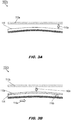
FIGS. 3A through 3C are diagrammatic cross sections illustrating induced warping operations of the IC package ofFIG. 1 ; -
FIG. 4 is a diagrammatic cross section illustrating operations on the IC package ofFIG. 1 ; and -
FIG. 5 is a flow diagram illustrating a method for induced warping of an IC package in accordance with example embodiments of this disclosure. - Before explaining one or more embodiments of the disclosure in detail, it is to be understood that the embodiments are not limited in their application to the details of construction and the arrangement of the components or steps or methodologies set forth in the following description or illustrated in the drawings. In the following detailed description of embodiments, numerous specific details may be set forth in order to provide a more thorough understanding of the disclosure. However, it will be apparent to one of ordinary skill in the art having the benefit of the instant disclosure that the embodiments disclosed herein may be practiced without some of these specific details. In other instances, well-known features may not be described in detail to avoid unnecessarily complicating the instant disclosure.
- As used herein a letter following a reference numeral is intended to reference an embodiment of the feature or element that may be similar, but not necessarily identical, to a previously described element or feature bearing the same reference numeral (e.g., 1, 1a, 1b). Such shorthand notations are used for purposes of convenience only and should not be construed to limit the disclosure in any way unless expressly stated to the contrary.
- Further, unless expressly stated to the contrary, "or" refers to an inclusive or and not to an exclusive or. For example, a condition A or B is satisfied by any one of the following: A is true (or present) and B is false (or not present), A is false (or not present) and B is true (or present), and both A and B are true (or present).
- In addition, use of "a" or "an" may be employed to describe elements and components of embodiments disclosed herein. This is done merely for convenience and "a" and "an" are intended to include "one" or "at least one," and the singular also includes the plural unless it is obvious that it is meant otherwise.
- Finally, as used herein any reference to "one embodiment" or "some embodiments" means that a particular element, feature, structure, or characteristic described in connection with the embodiment is included in at least one embodiment disclosed herein. The appearances of the phrase "in some embodiments" in various places in the specification are not necessarily all referring to the same embodiment, and embodiments may include one or more of the features expressly described or inherently present herein, or any combination or sub-combination of two or more such features, along with any other features which may not necessarily be expressly described or inherently present in the instant disclosure.
- Referring to
FIG. 1 , an integrated circuit (IC)package 100 is disclosed. Thesemiconducting die 100 may includeelectronic substrates 102 and anactive layer 104 upon which one or more semiconducting dies 106 and/or additional functional circuitry may be fabricated. - In embodiments, the
electronic substrates 102 may be fashioned of silicon or any other appropriate semiconducting material. Theactive layer 104 may include, for example, additive layers or other functional circuitry fabricated upon the electronic substrates 102 (e.g., onto an active side of the electronic substrate) or upon any additive layers deposited thereon, resulting in aninherent warping 108 toward the active layer (e.g., due to internal compressive stressed within the active layer). An induced warping stress may be imparted to theIC package 100 by utilizing thin film deposition (TFD) instrumentation to deposit (110) or bond one or morecorrective layers 112 on the inactive side (114) of the electronic substrates 102 (e.g., the side opposite the active layer/active side 104). As thecorrective layers 112 are applied to theinactive side 114 of the electronic substrates 102 (e.g., and condense thereon as thin films), the functionality of theactive layer 104 is unaffected. For example, depending on the desired degree of induced warping (and, e.g., the corresponding amount of compressive or tensile stress to induce within the active layer 104), thecorrective layers 112 may be deposited via physical vapor deposition (PVD), sputtering deposition, electroplating, or any other like instrumentation and process. - Referring also to
FIG. 2 , theIC package 100a may be implemented and may function similarly to theIC package 100 ofFIG. 1 , except that residual stresses within thecorrective layers 112 bonded to theinactive side 114 may induce compressive stresses (116a) and/or tensile stresses (116b) contributing to correctively warp (116) theelectronic substrates 102 of theIC package 100 ofFIG. 1 in the direction of theinactive side 114, such that theelectronic substrates 102 and/orsemiconducting die 106 are warped into a horizontal or near-horizontal orientation (as shown by theIC package 100a ofFIG. 2 ). - In embodiments, the precise direction and amount of induced warping necessary to achieve the substantially
horizontal IC package 100a may depend on a variety of parameters. For example, the material composition as well as the thickness and dimensions (e.g., x/y) of theelectronic substrates 102 and/orsemiconducting die 106 may affect the necessary direction and degree of inducedwarping 116 to correct the inherent warping (108,FIG. 1 ). Similarly, parameters may also be determined for optimal deposition of thecorrective layers 112. For example, thecorrective layers 112 may include copper or other metallic elements or compounds. In some embodiments, thecorrective layers 112 may include ceramic layers, metalloids, amorphous (e.g., glassy) semiconducting materials, or any appropriate combinations thereof. By selectingcorrective layers 112 of a particular thickness and depositing the corrective layers to theinactive side 114 at a particular deposition rate (e.g., between 5 Angstroms per second (Å/s) and 120 Å/s), significant corrective deflections of theelectronic substrates 102 may be achieved. For example, higher deposition rates ofcorrective layers 112 primarily comprising copper may be associated with higher residual stresses and therefore higher degrees of inducedwarping 116. Similarly, the number ofcorrective layers 112 deposited may be selected with a particular degree of inducedwarping 116 in mind, as described below. - In some embodiments, determination of the optimal deposition parameters and deposition of the
corrective layers 112 may occur during the active layer manufacturing phase of the production process of theIC package 100a. In other embodiments, parameter determination and deposition of thecorrective layers 112 may occur during other phases of the production process or based on other types ofIC package 100a, e.g., during reflow soldering or in response to warping issues associated with flip-chip packages and thin ball grid arrays. - Referring also to
FIGS. 3A through 3C , the IC packages 100b-c may be implemented and may function similarly to the IC packages 100, 100a ofFIGS. 1 and 2 , except that the IC packages 100b-c may incorporate multiplecorrective layers 112a-n deposited on theinactive side 114 via TFD (e.g., at lower deposition rates (e.g., 5 Å/s or less) so as to minimize impact stress). For example, referring in particular toFIG. 3A , a firstcorrective layer 112a may be bonded (110a) to theinactive side 114 of theIC package 100b at a particular deposition rate. Referring in particular toFIG. 3B , a secondcorrective layer 112b may be deposited upon (110b) or bonded to the firstcorrective layer 112a, inducing a further warping 116a-b of theIC package 100b. Referring in particular toFIG. 3C , the continued deposition of multiplecorrective layers 112a-n may provide, through each successive corrective layer, additional induced warping (116a-b) toward theinactive layer 114 such that the inherent warping (108,FIG. 1 ) of theIC package 100b may be reduced or even reversed, resulting in the substantiallyhorizontal IC package 100c shown byFIG. 3C . - Referring to
FIG. 4 , theIC package 100d may be implemented and may function similarly to the IC packages 100, 100a-c ofFIGS. 1 through 3C , except that one or morecorrective layers 112a-n may be removable layers configured for temporary induced warping. For example, an outercorrective layer 112n may be partially or fully removed (402) from theelectronic substrate 102, fully or partially relieving the corresponding internal compressive and tensile stresses and thereby relieving the corresponding induced warping (116a-b,FIGS. 3B-C ). - Referring to
FIG. 5 , themethod 500 for induced warping of an integrated circuit (IC) package may be implemented with respect to the IC packages 100, 100-d ofFIGS. 1 through 4 , and may incorporate the following steps. - At a
step 502, the degree of inherent warping toward the active side of an electronic substrate of the IC package due to the fabrication of a semiconducting die and/or functional circuitry on the active side is determined. For example, parameters associated with the semiconducting die or with the electronic substrates may be determined, e.g., the dimensions of the substrate, the thickness of the substrate, or the material composition of the substrate. - At a
step 504, a desired degree of induced warping stress toward the inactive side (e.g., opposite the active side) of the electronic substrate is determined. For example, the desired material composition of corrective layers applicable to the inactive side to correctively warp the substrate to the desired degree may be determined, as well as the desired number of layers to be applied (if more than one corrective layer is to be applied). - At a
step 506, the desired degree of induced warping stress is implemented by applying at least one corrective layer to the active side via thin film deposition (TFD). For example, the corrective layer/s may be applied at a predetermined deposition rate, or to a predetermined thickness, based on the determined parameters. - The
method 500 may include anadditional step 508. At thestep 508, a portion (partial or full) of the at least one applied corrective layer is partially or fully removed from the inactive side upon which it was deposited to remove the corresponding induced warping stress. - It is to be understood that embodiments of the methods disclosed herein may include one or more of the steps described herein. Further, such steps may be carried out in any desired order and two or more of the steps may be carried out simultaneously with one another. Two or more of the steps disclosed herein may be combined in a single step, and in some embodiments, one or more of the steps may be carried out as two or more sub-steps. Further, other steps or sub-steps may be carried in addition to, or as substitutes to one or more of the steps disclosed herein.
- Although inventive concepts have been described with reference to the embodiments illustrated in the attached drawing figures, equivalents may be employed and substitutions made herein without departing from the scope of the claims. Components illustrated and described herein are merely examples of a system/device and components that may be used to implement embodiments of the inventive concepts and may be replaced with other devices and components without departing from the scope of the claims. Furthermore, any dimensions, degrees, and/or numerical ranges provided herein are to be understood as non-limiting examples unless otherwise specified in the claims.
Claims (14)
- An integrated circuit, IC, package, comprising:at least one semiconducting die (100);an electronic substrate (102) having an active side (104) and an inactive side (114) opposite the active side, at least one of the semiconducting die and functional circuitry fabricated on the active side,at least one of the semiconducting die and the electronic substrate associated with an inherent warping toward the active side,andthe inactive side (114) having at least one corrective layer (112) deposited thereupon via thin film deposition, TFD, the at least one corrective layer configured for desired induced warping of the electronic substrate toward the inactive layer.
- The IC package of claim 1, wherein the at least one corrective layer is deposited based on at least one predetermined parameter.
- The IC package of claim 2, wherein the at least one corrective layer has a predetermined thickness based on the at least one predetermined parameter.
- The IC package of claim 2, wherein the at least one corrective layer is deposited at a predetermined rate based on the at least one predetermined parameter.
- The IC package of claim 2, 3 or 4, wherein the at least one predetermined parameter corresponds to at least one of the semiconducting die, the electronic substrate, and the inherent warping.
- The IC package of claim 2, 3 or 4, wherein the at least one predetermined parameter corresponds to at least one of the corrective layer and the desired induced warping.
- The IC package of any preceding claim, wherein the at least one corrective layer includes at least one of:a ceramic layer;an amorphous semiconducting layer;a metalloid layer; anda metallic layer.
- The IC package of any preceding claim, wherein:the desired induced warping includes a temporary induced warping:andthe at least one corrective layer is at least partially removable.
- The IC package of any preceding claim, wherein the IC package includes at least one of a flip-chip assembly and a ball grid array.
- A method for induced warping of an integrated circuit, IC, package, the method comprising:determining a degree of inherent warping toward an active side of an electronic substrate, the inherent warping associated with the fabrication of at least one of a semiconducting die and functional circuitry upon the active side;determining a degree of desired induced warping stress toward an inactive side of the electronic substrate, the inactive side opposite the active side;andimplementing the desired induced warping stress by applying, via thin film deposition,TFD, at least one corrective layer to the inactive side.
- The method of claim 10, wherein:determining a degree of desired induced warping stress toward an inactive side of the electronic substrate, the inactive side opposite the active side, includes: determining at least one parameter corresponding to at least one of the semiconducting die, the electronic substrate, the degree of inherent warping, the electronic substrate, and the desired induced warping stress;andimplementing the desired induced warping stress by applying, via thin film deposition, TFD, at least one corrective layer to the inactive side includes: applying the at least one corrective layer to the inactive side based on the at least one determined parameter.
- The method of claim 11, wherein implementing the desired induced warping stress by applying, via thin film deposition, TFD, at least one corrective layer to the inactive side includes:
applying the at least one corrective layer at a predetermined rate based on the at least one determined parameter. - The method of claim 11, wherein implementing the desired induced warping stress by applying, via thin film deposition, TFD, at least one corrective layer to the inactive side includes:
applying the at least one corrective layer to a predetermined thickness based on the at least one determined parameter. - The method of any of claims 10 to 13, further comprising:
at least partially restoring the inherent warping by at least partially removing the at least one corrective layer.
Applications Claiming Priority (1)
| Application Number | Priority Date | Filing Date | Title |
|---|---|---|---|
| US16/750,382 US11239182B2 (en) | 2020-01-23 | 2020-01-23 | Controlled induced warping of electronic substrates |
Publications (1)
| Publication Number | Publication Date |
|---|---|
| EP3855480A1 true EP3855480A1 (en) | 2021-07-28 |
Family
ID=74236064
Family Applications (1)
| Application Number | Title | Priority Date | Filing Date |
|---|---|---|---|
| EP21153263.5A Pending EP3855480A1 (en) | 2020-01-23 | 2021-01-25 | Controlled induced warping of electronic substrates |
Country Status (2)
| Country | Link |
|---|---|
| US (1) | US11239182B2 (en) |
| EP (1) | EP3855480A1 (en) |
Citations (5)
| Publication number | Priority date | Publication date | Assignee | Title |
|---|---|---|---|---|
| US20050253235A1 (en) * | 2004-05-11 | 2005-11-17 | Kazumi Hara | Semiconductor chip and circuit board, manufacturing method of same, and electronic equipment |
| US20100013077A1 (en) * | 2008-07-21 | 2010-01-21 | Samsaung Electronics Co., Ltd. | Semiconductor device |
| US20150115393A1 (en) * | 2012-01-27 | 2015-04-30 | Skyworks Solutions, Inc. | Methods of stress balancing in gallium arsenide wafer processing |
| US20150155242A1 (en) * | 2013-12-03 | 2015-06-04 | United Microelectronics Corporation | Integrated semiconductor device and method for fabricating the same |
| US20180082960A1 (en) * | 2016-09-16 | 2018-03-22 | Ii-Vi Optoelectronic Devices, Inc. | Metallic, tunable thin film stress compensation for epitaxial wafers |
Family Cites Families (15)
| Publication number | Priority date | Publication date | Assignee | Title |
|---|---|---|---|---|
| JP2000012744A (en) * | 1998-06-19 | 2000-01-14 | Fujitsu Ltd | Semiconductor device and manufacturing method thereof |
| US6507100B1 (en) | 2000-06-28 | 2003-01-14 | Advanced Micro Devices, Inc. | Cu-balanced substrate |
| JP2002368224A (en) | 2001-06-04 | 2002-12-20 | Sony Corp | Functional device and method of manufacturing the same |
| US7449780B2 (en) | 2003-03-31 | 2008-11-11 | Intel Corporation | Apparatus to minimize thermal impedance using copper on die backside |
| US20100109169A1 (en) | 2008-04-29 | 2010-05-06 | United Test And Assembly Center Ltd | Semiconductor package and method of making the same |
| CN104137257B (en) | 2011-12-21 | 2017-11-21 | 英特尔公司 | The semiconductor element and CTE engineering tube cores pair of encapsulation |
| US9048298B1 (en) | 2012-03-29 | 2015-06-02 | Amkor Technology, Inc. | Backside warpage control structure and fabrication method |
| US10134689B1 (en) | 2013-02-28 | 2018-11-20 | Maxim Integrated Products, Inc. | Warpage compensation metal for wafer level packaging technology |
| US9601406B2 (en) | 2013-03-01 | 2017-03-21 | Intel Corporation | Copper nanorod-based thermal interface material (TIM) |
| US9184041B2 (en) | 2013-06-25 | 2015-11-10 | Taiwan Semiconductor Manufacturing Co., Ltd. | Integrated circuit with backside structures to reduce substrate warp |
| US9967971B2 (en) | 2015-11-12 | 2018-05-08 | International Business Machines Corporation | Method of reducing warpage of an orgacnic substrate |
| US10170339B2 (en) * | 2016-10-25 | 2019-01-01 | Nanya Technology Corporation | Semiconductor structure and a manufacturing method thereof |
| WO2019005152A1 (en) | 2017-06-30 | 2019-01-03 | Intel Corporation | Die back side structures for warpage control |
| US20190206753A1 (en) | 2017-12-30 | 2019-07-04 | Intel Corporation | Bicontinuous porous ceramic composite for semiconductor package applications |
| US10504858B2 (en) | 2018-04-27 | 2019-12-10 | Taiwan Semiconductor Manufacturing Co., Ltd. | Package structure and method of fabricating the same |
-
2020
- 2020-01-23 US US16/750,382 patent/US11239182B2/en active Active
-
2021
- 2021-01-25 EP EP21153263.5A patent/EP3855480A1/en active Pending
Patent Citations (6)
| Publication number | Priority date | Publication date | Assignee | Title |
|---|---|---|---|---|
| US20050253235A1 (en) * | 2004-05-11 | 2005-11-17 | Kazumi Hara | Semiconductor chip and circuit board, manufacturing method of same, and electronic equipment |
| US7387945B2 (en) * | 2004-05-11 | 2008-06-17 | Seiko Epson Corporation | Semiconductor chip, semiconductor device and electronic equipment including warpage control film, and manufacturing method of same |
| US20100013077A1 (en) * | 2008-07-21 | 2010-01-21 | Samsaung Electronics Co., Ltd. | Semiconductor device |
| US20150115393A1 (en) * | 2012-01-27 | 2015-04-30 | Skyworks Solutions, Inc. | Methods of stress balancing in gallium arsenide wafer processing |
| US20150155242A1 (en) * | 2013-12-03 | 2015-06-04 | United Microelectronics Corporation | Integrated semiconductor device and method for fabricating the same |
| US20180082960A1 (en) * | 2016-09-16 | 2018-03-22 | Ii-Vi Optoelectronic Devices, Inc. | Metallic, tunable thin film stress compensation for epitaxial wafers |
Also Published As
| Publication number | Publication date |
|---|---|
| US20210233866A1 (en) | 2021-07-29 |
| US11239182B2 (en) | 2022-02-01 |
Similar Documents
| Publication | Publication Date | Title |
|---|---|---|
| US5407863A (en) | Method of manufacturing semiconductor device | |
| KR100313706B1 (en) | Redistributed Wafer Level Chip Size Package And Method For Manufacturing The Same | |
| KR102478822B1 (en) | Semiconductor device with anti-warp layer | |
| US20200091089A1 (en) | Silicon wafer manufacturing method | |
| JP4466925B2 (en) | Barrier film for flexible copper substrate and sputtering target for barrier film formation | |
| EP2158601A1 (en) | Under bump metallization structure having a seed layer for electroless nickel deposition | |
| JP2004185890A (en) | Metal mask | |
| JP3975439B2 (en) | Metal mask | |
| US11239182B2 (en) | Controlled induced warping of electronic substrates | |
| KR102716370B1 (en) | Mask-support assembly and producing method thereof | |
| US7675286B2 (en) | Magnetoresistive sensor device | |
| FI61588C (en) | FOERFARANDE FOER UTFOERANDE AV ELEKTRISKT LEDANDE GENOMFOERINGAR I TUNNFILMER | |
| US20130328203A1 (en) | Method for applying a final metal layer for wafer level packaging and associated device | |
| DE112014006817T5 (en) | Transducer element and method of manufacturing a transducer element | |
| US7166921B2 (en) | Aluminum alloy film for wiring and sputter target material for forming the film | |
| EP3855481A1 (en) | Controlled induced warping of electronic substrates via electroplating | |
| KR20120115130A (en) | Manufacturing method of semiconductor device and semiconductor device | |
| KR20120040749A (en) | Method for forming cu wiring | |
| TW201307184A (en) | Thin film structure for high density inductance and redistribution in wafer level packaging | |
| KR102142752B1 (en) | Fe-Ni BASED FOIL HAVING RESIN ADHESION, METHOD FOR PREPARING THE Fe-Ni BASED FOIL, MASK FOR DEPOSITION AND METHOD FOR PREPARING THE MASK | |
| US6083375A (en) | Process for producing corrosion-resistant terminal metal pads for thin film packages | |
| JPH0414821A (en) | Manufacture of semiconductor device | |
| US8252363B2 (en) | Method of thinning a block transferred to a substrate | |
| JPH06310512A (en) | Copper wiring and its formation | |
| KR20190045189A (en) | Method of manufacturing silicon epitaxial wafer and method of manufacturing semiconductor device |
Legal Events
| Date | Code | Title | Description |
|---|---|---|---|
| PUAI | Public reference made under article 153(3) epc to a published international application that has entered the european phase |
Free format text: ORIGINAL CODE: 0009012 |
|
| STAA | Information on the status of an ep patent application or granted ep patent |
Free format text: STATUS: THE APPLICATION HAS BEEN PUBLISHED |
|
| AK | Designated contracting states |
Kind code of ref document: A1 Designated state(s): AL AT BE BG CH CY CZ DE DK EE ES FI FR GB GR HR HU IE IS IT LI LT LU LV MC MK MT NL NO PL PT RO RS SE SI SK SM TR |
|
| STAA | Information on the status of an ep patent application or granted ep patent |
Free format text: STATUS: REQUEST FOR EXAMINATION WAS MADE |
|
| 17P | Request for examination filed |
Effective date: 20220128 |
|
| RBV | Designated contracting states (corrected) |
Designated state(s): AL AT BE BG CH CY CZ DE DK EE ES FI FR GB GR HR HU IE IS IT LI LT LU LV MC MK MT NL NO PL PT RO RS SE SI SK SM TR |
|
| STAA | Information on the status of an ep patent application or granted ep patent |
Free format text: STATUS: EXAMINATION IS IN PROGRESS |
|
| 17Q | First examination report despatched |
Effective date: 20250306 |