EP3855415B1 - Display device - Google Patents
Display device Download PDFInfo
- Publication number
- EP3855415B1 EP3855415B1 EP19881855.1A EP19881855A EP3855415B1 EP 3855415 B1 EP3855415 B1 EP 3855415B1 EP 19881855 A EP19881855 A EP 19881855A EP 3855415 B1 EP3855415 B1 EP 3855415B1
- Authority
- EP
- European Patent Office
- Prior art keywords
- facet
- drive board
- display device
- housing
- display panel
- Prior art date
- Legal status (The legal status is an assumption and is not a legal conclusion. Google has not performed a legal analysis and makes no representation as to the accuracy of the status listed.)
- Active
Links
Images


Classifications
-
- G—PHYSICS
- G09—EDUCATION; CRYPTOGRAPHY; DISPLAY; ADVERTISING; SEALS
- G09F—DISPLAYING; ADVERTISING; SIGNS; LABELS OR NAME-PLATES; SEALS
- G09F9/00—Indicating arrangements for variable information in which the information is built-up on a support by selection or combination of individual elements
-
- G—PHYSICS
- G09—EDUCATION; CRYPTOGRAPHY; DISPLAY; ADVERTISING; SEALS
- G09F—DISPLAYING; ADVERTISING; SIGNS; LABELS OR NAME-PLATES; SEALS
- G09F9/00—Indicating arrangements for variable information in which the information is built-up on a support by selection or combination of individual elements
- G09F9/30—Indicating arrangements for variable information in which the information is built-up on a support by selection or combination of individual elements in which the desired character or characters are formed by combining individual elements
-
- G—PHYSICS
- G02—OPTICS
- G02F—OPTICAL DEVICES OR ARRANGEMENTS FOR THE CONTROL OF LIGHT BY MODIFICATION OF THE OPTICAL PROPERTIES OF THE MEDIA OF THE ELEMENTS INVOLVED THEREIN; NON-LINEAR OPTICS; FREQUENCY-CHANGING OF LIGHT; OPTICAL LOGIC ELEMENTS; OPTICAL ANALOGUE/DIGITAL CONVERTERS
- G02F1/00—Devices or arrangements for the control of the intensity, colour, phase, polarisation or direction of light arriving from an independent light source, e.g. switching, gating or modulating; Non-linear optics
- G02F1/01—Devices or arrangements for the control of the intensity, colour, phase, polarisation or direction of light arriving from an independent light source, e.g. switching, gating or modulating; Non-linear optics for the control of the intensity, phase, polarisation or colour
- G02F1/13—Devices or arrangements for the control of the intensity, colour, phase, polarisation or direction of light arriving from an independent light source, e.g. switching, gating or modulating; Non-linear optics for the control of the intensity, phase, polarisation or colour based on liquid crystals, e.g. single liquid crystal display cells
- G02F1/133—Constructional arrangements; Operation of liquid crystal cells; Circuit arrangements
- G02F1/1333—Constructional arrangements; Manufacturing methods
- G02F1/133308—Support structures for LCD panels, e.g. frames or bezels
-
- G—PHYSICS
- G02—OPTICS
- G02F—OPTICAL DEVICES OR ARRANGEMENTS FOR THE CONTROL OF LIGHT BY MODIFICATION OF THE OPTICAL PROPERTIES OF THE MEDIA OF THE ELEMENTS INVOLVED THEREIN; NON-LINEAR OPTICS; FREQUENCY-CHANGING OF LIGHT; OPTICAL LOGIC ELEMENTS; OPTICAL ANALOGUE/DIGITAL CONVERTERS
- G02F1/00—Devices or arrangements for the control of the intensity, colour, phase, polarisation or direction of light arriving from an independent light source, e.g. switching, gating or modulating; Non-linear optics
- G02F1/01—Devices or arrangements for the control of the intensity, colour, phase, polarisation or direction of light arriving from an independent light source, e.g. switching, gating or modulating; Non-linear optics for the control of the intensity, phase, polarisation or colour
- G02F1/13—Devices or arrangements for the control of the intensity, colour, phase, polarisation or direction of light arriving from an independent light source, e.g. switching, gating or modulating; Non-linear optics for the control of the intensity, phase, polarisation or colour based on liquid crystals, e.g. single liquid crystal display cells
- G02F1/133—Constructional arrangements; Operation of liquid crystal cells; Circuit arrangements
- G02F1/1333—Constructional arrangements; Manufacturing methods
- G02F1/133308—Support structures for LCD panels, e.g. frames or bezels
- G02F1/13332—Front frames
-
- G—PHYSICS
- G02—OPTICS
- G02F—OPTICAL DEVICES OR ARRANGEMENTS FOR THE CONTROL OF LIGHT BY MODIFICATION OF THE OPTICAL PROPERTIES OF THE MEDIA OF THE ELEMENTS INVOLVED THEREIN; NON-LINEAR OPTICS; FREQUENCY-CHANGING OF LIGHT; OPTICAL LOGIC ELEMENTS; OPTICAL ANALOGUE/DIGITAL CONVERTERS
- G02F1/00—Devices or arrangements for the control of the intensity, colour, phase, polarisation or direction of light arriving from an independent light source, e.g. switching, gating or modulating; Non-linear optics
- G02F1/01—Devices or arrangements for the control of the intensity, colour, phase, polarisation or direction of light arriving from an independent light source, e.g. switching, gating or modulating; Non-linear optics for the control of the intensity, phase, polarisation or colour
- G02F1/13—Devices or arrangements for the control of the intensity, colour, phase, polarisation or direction of light arriving from an independent light source, e.g. switching, gating or modulating; Non-linear optics for the control of the intensity, phase, polarisation or colour based on liquid crystals, e.g. single liquid crystal display cells
- G02F1/133—Constructional arrangements; Operation of liquid crystal cells; Circuit arrangements
- G02F1/1333—Constructional arrangements; Manufacturing methods
- G02F1/1345—Conductors connecting electrodes to cell terminals
- G02F1/13452—Conductors connecting driver circuitry and terminals of panels
-
- H—ELECTRICITY
- H05—ELECTRIC TECHNIQUES NOT OTHERWISE PROVIDED FOR
- H05K—PRINTED CIRCUITS; CASINGS OR CONSTRUCTIONAL DETAILS OF ELECTRIC APPARATUS; MANUFACTURE OF ASSEMBLAGES OF ELECTRICAL COMPONENTS
- H05K1/00—Printed circuits
- H05K1/02—Details
- H05K1/0277—Bendability or stretchability details
- H05K1/028—Bending or folding regions of flexible printed circuits
-
- G—PHYSICS
- G02—OPTICS
- G02F—OPTICAL DEVICES OR ARRANGEMENTS FOR THE CONTROL OF LIGHT BY MODIFICATION OF THE OPTICAL PROPERTIES OF THE MEDIA OF THE ELEMENTS INVOLVED THEREIN; NON-LINEAR OPTICS; FREQUENCY-CHANGING OF LIGHT; OPTICAL LOGIC ELEMENTS; OPTICAL ANALOGUE/DIGITAL CONVERTERS
- G02F1/00—Devices or arrangements for the control of the intensity, colour, phase, polarisation or direction of light arriving from an independent light source, e.g. switching, gating or modulating; Non-linear optics
- G02F1/01—Devices or arrangements for the control of the intensity, colour, phase, polarisation or direction of light arriving from an independent light source, e.g. switching, gating or modulating; Non-linear optics for the control of the intensity, phase, polarisation or colour
- G02F1/13—Devices or arrangements for the control of the intensity, colour, phase, polarisation or direction of light arriving from an independent light source, e.g. switching, gating or modulating; Non-linear optics for the control of the intensity, phase, polarisation or colour based on liquid crystals, e.g. single liquid crystal display cells
- G02F1/133—Constructional arrangements; Operation of liquid crystal cells; Circuit arrangements
- G02F1/1333—Constructional arrangements; Manufacturing methods
- G02F1/133308—Support structures for LCD panels, e.g. frames or bezels
- G02F1/133328—Segmented frames
-
- G—PHYSICS
- G02—OPTICS
- G02F—OPTICAL DEVICES OR ARRANGEMENTS FOR THE CONTROL OF LIGHT BY MODIFICATION OF THE OPTICAL PROPERTIES OF THE MEDIA OF THE ELEMENTS INVOLVED THEREIN; NON-LINEAR OPTICS; FREQUENCY-CHANGING OF LIGHT; OPTICAL LOGIC ELEMENTS; OPTICAL ANALOGUE/DIGITAL CONVERTERS
- G02F1/00—Devices or arrangements for the control of the intensity, colour, phase, polarisation or direction of light arriving from an independent light source, e.g. switching, gating or modulating; Non-linear optics
- G02F1/01—Devices or arrangements for the control of the intensity, colour, phase, polarisation or direction of light arriving from an independent light source, e.g. switching, gating or modulating; Non-linear optics for the control of the intensity, phase, polarisation or colour
- G02F1/13—Devices or arrangements for the control of the intensity, colour, phase, polarisation or direction of light arriving from an independent light source, e.g. switching, gating or modulating; Non-linear optics for the control of the intensity, phase, polarisation or colour based on liquid crystals, e.g. single liquid crystal display cells
- G02F1/133—Constructional arrangements; Operation of liquid crystal cells; Circuit arrangements
- G02F1/1333—Constructional arrangements; Manufacturing methods
- G02F1/133308—Support structures for LCD panels, e.g. frames or bezels
- G02F1/133334—Electromagnetic shields
-
- G—PHYSICS
- G02—OPTICS
- G02F—OPTICAL DEVICES OR ARRANGEMENTS FOR THE CONTROL OF LIGHT BY MODIFICATION OF THE OPTICAL PROPERTIES OF THE MEDIA OF THE ELEMENTS INVOLVED THEREIN; NON-LINEAR OPTICS; FREQUENCY-CHANGING OF LIGHT; OPTICAL LOGIC ELEMENTS; OPTICAL ANALOGUE/DIGITAL CONVERTERS
- G02F2202/00—Materials and properties
- G02F2202/28—Adhesive materials or arrangements
-
- H—ELECTRICITY
- H05—ELECTRIC TECHNIQUES NOT OTHERWISE PROVIDED FOR
- H05K—PRINTED CIRCUITS; CASINGS OR CONSTRUCTIONAL DETAILS OF ELECTRIC APPARATUS; MANUFACTURE OF ASSEMBLAGES OF ELECTRICAL COMPONENTS
- H05K2201/00—Indexing scheme relating to printed circuits covered by H05K1/00
- H05K2201/10—Details of components or other objects attached to or integrated in a printed circuit board
- H05K2201/10007—Types of components
- H05K2201/10128—Display
Definitions
- This application relates to the field of electronic technologies, and in particular, to a display device.
- a drive board that drives a display panel of the display device to perform display is parallel to the display panel and is disposed at a location of a lower bezel of the display device.
- a width of the lower bezel is restricted by a width of the drive board.
- International patent application WO 2013/089030 A1 discloses a display device with: a display panel having on the front side a display region on which an image is displayed, and a frame-like non-display region for surrounding the display region; a drive substrate for controlling the display and drive operations of the display panel; a flexible wire which electrically connects the display panel with the drive substrate and which is folded so that the drive substrate is disposed on the front side of the display panel; and a frame which has a frame-shaped main body disposed on the front side of the display panel so as to cover the non-display region, and a storage part disposed within the frame-like main body and for storing the drive substrate.
- This application provides a display device on which a narrow bezel can be implemented.
- the display device includes a display part.
- the display part includes a display panel, a bezel, a drive board, and a flexible printed circuit board electrically connected to the display panel and the drive board.
- the bezel is located on one side of the display panel and protrudes relative to a surface on which the display panel is located.
- An accommodating cavity is provided in the bezel.
- the drive board is fixed in the accommodating cavity, and the drive board and the display panel are disposed at an included angle.
- the drive board includes a front facet on which a connection line is disposed and a back facet.
- the flexible printed circuit board includes a first end, a second end, and a fixed section located between the first end and the second end. The second end is fixedly connected to the display panel.
- the fixed section is fixed to the back facet and faces the display panel.
- the first end is fixed to the front facet and is away from the display panel.
- the drive board is disposed in the accommodating cavity, and the drive board and the display panel are disposed at the included angle. Therefore, the drive board and the display panel are disposed in a non-parallel manner, so that a projection of the drive board on a plane on which the display panel is located is reduced, and a width of a bezel used to cover the drive board can be reduced.
- the first end of the flexible printed circuit board is fixed to the front facet of the drive board and is electrically connected to the connection line, and the fixed section is fixed to the back facet of the drive board, so that when the flexible printed circuit board is subsequently pulled, a force-bearing location on the flexible printed circuit board is the fixed section, and the first end is not pulled, thereby preventing the first end from being detached from the drive board due to pulling.
- a section between the fixed section and the second end of the flexible printed circuit board is curved, so that a length of the flexible printed circuit board between the drive board and the display panel is greater than a distance between the drive board and the display panel, and the flexible printed circuit board has specific stretching space, thereby avoiding damage to the flexible printed circuit board due to pulling in a process in which the flexible printed circuit board is electrically connected to the drive board and the display panel, and facilitating installation of the drive board and the flexible printed circuit board in the display device.
- the included angle between the drive board and the display panel is greater than or equal to 90°, to minimize the projection of the drive board on the plane on which the display panel is located, and minimize the width of the bezel.
- the included angle between the drive board and the display panel is greater than or equal to 90°, so that an angle formed by bending the section between the second end and the fixed section of the flexible printed circuit board is greater than or equal to 90°, thereby avoiding damage to the flexible printed circuit board due to an excessively large bending degree of the flexible printed circuit board.
- the fixed section is fixed to the back facet by using an adhesive
- the drive board includes a bottom facet and a top facet that are connected to the front facet and the back facet and that are disposed opposite to each other, the bottom facet is close to the display panel
- the flexible printed circuit board extends from the front facet to the back facet through the top facet
- a thickness of the adhesive gradually increases in a direction from the top facet to the bottom facet.
- the thickness of the adhesive gradually increases in the direction from the top facet to the bottom facet, so that a specific angle is formed between the fixed section and the back facet, to increase the angle formed by bending the section between the second end and the fixed section of the flexible printed circuit board. Therefore, a bending degree of the flexible printed circuit board can be further reduced, thereby avoiding damage to the flexible printed circuit board due to an excessively large bending degree of the flexible printed circuit board.
- the adhesive may include a plurality of sub-areas disposed at intervals in the direction from the top facet to the bottom facet.
- the plurality of sub-areas are used to fix the fixed section at a plurality of points, to achieve a better fixing effect.
- a section, between adjacent sub-areas, of the fixed section is curved, so that when one fixing point is detached, the curved fixed section can provide stretching space to avoid further detaching of another fixing point.
- the drive board includes a bottom facet and a top facet that are connected to the front facet and the back facet and that are disposed opposite to each other, the bottom facet is close to the display panel, a groove is recessed on the top facet in a direction towards the bottom facet, and a part of the flexible printed circuit board is accommodated in the groove.
- the groove is provided on the top facet of the drive board, and the flexible printed circuit board extends to the back facet through the groove, so that the flexible printed circuit board does not protrude at an edge of the flexible printed circuit board when bypassing the drive board, thereby avoiding damage caused to the flexible printed circuit board by an inner wall of the accommodating cavity when the drive board is fixed in the accommodating cavity.
- a fixing structure such as an adhesive may be disposed in the groove, so that a part of the flexible printed circuit board is fixed in the groove, thereby further avoiding detaching between the first end and the front facet when the flexible printed circuit board is pulled.
- a through-hole is provided on the drive board, and a section between the first end and the fixed section of the flexible printed circuit board passes the through-hole to extend to the back facet, so that a length of the flexible printed circuit board can be shortened, and damage caused to the flexible printed circuit board by the inner wall of the accommodating cavity can also be avoided.
- a buffer piece is disposed between the drive board and an inner wall of the bezel.
- the buffer piece provides buffering between the drive board and an inner wall of the protrusion, to avoid collision between the drive board and the inner wall of the protrusion when the display device encounters collision, and therefore avoid damage to the drive board.
- the bezel is made of a signal shielding material, or a shield layer is disposed on the inner wall or an outer wall of the protrusion, to shield an external signal by using the protrusion, and avoid interference from the external signal to a signal transmitted by the drive board.
- the display device includes a backplane
- the bezel protrudes relative to a surface on which the display panel is located to form a protrusion
- the protrusion includes a first housing and a second housing
- the first housing and the second housing are detachably fixed on the backplane
- the first housing, the second housing, and the backplane enclose the accommodating cavity.
- the protrusion is disposed as a structure including the first housing and the second housing.
- a front retaining wall and a rear retaining wall spaced apart from the front retaining wall are disposed on the backplane, one side of the drive board is sandwiched between the front retaining wall and the rear retaining wall, support ribs are disposed on inner walls of the first housing and the second housing, a first surface of the drive board is carried on the support rib of the first housing, and a second surface of the drive board is carried on the support rib of the second housing.
- the display device includes a rotating shaft and a functional part, the rotating shaft is accommodated in the accommodating cavity, and the rotating shaft is connected to the display part and the functional part, so that the display part and the functional part are rotatably connected.
- the rotating shaft is disposed in the protrusion, so that a structure of the display device is simplified.
- the rotating shaft is rotatably connected to the display part and the functional part, so that the display part and the functional part can be folded relative to each other, thereby extending a use function of the display device.
- the display device may be a notebook computer, or may be a display device such as a television or a tablet computer.
- the display device includes a display part 100.
- the display part 100 includes a display panel 10, a drive board 20, and a flexible printed circuit board 30 electrically connected to the display panel 10 and the drive board 20.
- the drive board 20 provides a drive signal for the display panel 10 by using the flexible printed circuit board 30, to drive the display panel 10 to perform display.
- a bezel 40 is disposed around the display panel 10. On one side of the display panel 10, the bezel 40 protrudes from a surface on which the display panel 10 is located to form a protrusion 50.
- the display panel 10 is a quadrilateral panel and includes four side edges.
- the bezel 40 includes an upper bezel 41, a lower bezel 42 opposite to the upper bezel 41, and a left bezel 43 and a right bezel 44 located between the upper bezel 41 and the lower bezel 42.
- the upper bezel 41, the lower bezel 42, the left bezel 43, and the right bezel 44 are separately located on sides at the four side edges of the display panel 10.
- the lower bezel 42 protrudes from the surface on which the display panel 10 is located to form the protrusion 50.
- An accommodating cavity 51 is formed in the protrusion 50.
- the drive board 20 is fixed in the accommodating cavity 51, and the drive board 20 and the display panel 10 are disposed at an included angle. That the drive board 20 and the display panel 10 are disposed at an included angle means that the drive board 20 and the display panel 10 are disposed at a specific included angle.
- the drive board 20 is disposed in the accommodating cavity 51 of the protrusion 50 that protrudes from a plane on which the display panel 10 is located, so that the drive board 20 and the display panel 10 can be disposed at the included angle. Therefore, a projection of the drive board 20 on the plane on which the display panel 10 is located is reduced, and a width of the bezel 40 used to cover the drive board 20 can be reduced.
- the drive board 20 includes a front facet 21 and a back facet 22 opposite to the front facet 21.
- the drive board 20 is a PCB.
- the PCB board may be a single-sided PCB board, or may be a double-sided PCB or a multi-layer PCB.
- the drive board 20 is a single-sided PCB, and a connection line is disposed on the front facet of the drive board 20.
- the flexible printed circuit board 30 includes a first end 31 fixed to the front facet 21 of the drive board 20, a second end 32 connected to the display panel 10, and a fixed section 33 located between the first end 31 and the second end 32.
- the fixed section 33 is fixed to the back facet 22 of the drive board 20.
- the first end 31 of the flexible printed circuit board 30 is fixed to the front facet 21 and is electrically connected to the connection line on the front facet 21, to provide a display signal for the display panel 10 through the connection line.
- the flexible printed circuit board 30 extends from the front facet 21 to the back facet 22 through a side facet of the drive board 20, and the fixed section 33 is fixed to the back facet 22, so that when the flexible printed circuit board 30 is subsequently pulled, a force-bearing location on the flexible printed circuit board 30 is the fixed section 33, and the first end 31 is not pulled, thereby preventing the first end 31 from being detached from the drive board 20 due to pulling.
- Manners of fixing the fixed section 33 to the back facet 22 include but are not limited to fixing by using bonding glue such as an adhesive, clamping, and other fixing manners.
- the fixed section 33 is fixed to the back facet 22 by using an adhesive 34.
- the drive board 20 includes a bottom facet 24 and a top facet 25 that are connected to the front facet 21 and the back facet 22 and that are disposed opposite to each other.
- the bottom facet 24 is close to the display panel 10.
- the flexible printed circuit board 30 extends from the front facet 21 to the back facet 22 through the top facet 25.
- a thickness of the adhesive 34 gradually increases in a direction from the top facet 25 to the bottom facet 24.
- the thickness of the adhesive gradually increases in the direction from the top facet 25 to the bottom facet 24, so that a specific angle is formed between the fixed section 33 and the back facet 22, to increase an angle formed by bending a section between the second end 32 and the fixed section 33 of the flexible printed circuit board 30. Therefore, a bending degree of the flexible printed circuit board 30 can be further reduced, thereby avoiding damage to the flexible printed circuit board 30 due to an excessively large bending degree of the flexible printed circuit board 30.
- the adhesive 34 may include a plurality of sub-areas 341 disposed at intervals in the direction from the top facet 25 to the bottom facet 24.
- the plurality of sub-areas 341 are used to fix the fixed section 33 at a plurality of points, to achieve a better fixing effect.
- a section, between adjacent sub-areas 341, of the fixed section 33 is curved, so that when one fixing point is detached, the curved fixed section 33 can provide stretching space to avoid further detaching of another fixing point, to achieve a better fixing effect.
- a groove 23 is provided at a side edge of the drive board 20, and a section between the first end 31 and the fixed section 33 of the flexible printed circuit board 30 extends from the front facet 21 to the back facet 22 through the groove 23.
- the groove 23 is provided at the side edge of the drive board 20, and the flexible printed circuit board 30 extends to the back facet 22 through the groove 23, so that the flexible printed circuit board 30 does not protrude at an edge of the flexible printed circuit board 30 when bypassing the drive board 20, thereby avoiding damage caused to the flexible printed circuit board 30 by an inner wall of the accommodating cavity 51 when the drive board 20 is fixed in the accommodating cavity 51.
- a length of the groove 23 is the same as a width of the flexible printed circuit board 30, so that when the flexible printed circuit board 30 extends to the back facet 22 through the groove 23, the flexible printed circuit board 30 is properly clamped in the groove 23. This avoids a case in which a portion between the first end 31 and the fixed section 33 moves along a length direction of the drive board 20 and therefore the first end 31 is detached from the drive board 20.
- the length direction of the drive board 20 is the same as a length direction of an edge, corresponding to the lower bezel 42, of the display panel.
- a fixing structure such as an adhesive may be disposed in the groove 23, so that a part of the flexible printed circuit board 30 is fixed in the groove 23, thereby further avoiding detaching between the first end 31 and the front facet 21 when the flexible printed circuit board 30 is pulled.
- a through-hole is provided on the drive board 20, and a section between the first end 31 and the fixed section 33 of the flexible printed circuit board 30 passes the through-hole to extend to the back facet 22, so that a length of the flexible printed circuit board 30 can be shortened.
- the flexible printed circuit board 30 can be prevented from protruding at an edge of the flexible printed circuit board 30 when bypassing the drive board 20, thereby avoiding damage caused to the flexible printed circuit board 30 by an inner wall of the accommodating cavity 51 when the drive board 20 is fixed in the accommodating cavity 51.
- a length direction of the through-hole is the same as a length direction of the drive board 20, and a length of the through-hole is the same as a width of the flexible printed circuit board 30, so that when the flexible printed circuit board 30 extends to the back facet 22 through the through-hole, the flexible printed circuit board 30 is properly clamped in the through-hole. This avoids a case in which a portion between the first end 31 and the fixed section 33 moves along the length direction of the drive board 20 and therefore the first end 31 is detached from the drive board 20.
- a section between the fixed section 33 and the second end 32 of the flexible printed circuit board 30 is curved, so that a length of the flexible printed circuit board 30 between the drive board 20 and the display panel 10 is greater than a distance between the drive board 20 and the display panel 10, and the flexible printed circuit board 30 has specific stretching space, thereby avoiding damage to the flexible printed circuit board 30 due to pulling in a process in which the flexible printed circuit board 30 is electrically connected to the drive board 20 and the display panel 10.
- the included angle between the drive board 20 and the display panel 10 is greater than or equal to 90°, to minimize the projection of the drive board 20 on the plane on which the display panel 10 is located, and minimize the width of the bezel 40.
- the included angle between the drive board 20 and the display panel 10 is greater than or equal to 90°, so that an angle formed by bending the section between the fixed section 33 and the second end 32 of the flexible printed circuit board 30 is greater than or equal to 90°, thereby avoiding damage to the flexible printed circuit board 30 due to an excessively large bending degree of the flexible printed circuit board 30.
- the included angle between the drive board 20 and the display panel 10 is 90°, so that the width of the bezel 40 is minimized.
- a buffer piece 60 is disposed between the drive board 20 and an inner wall of the protrusion 50.
- the buffer piece 60 provides buffering between the drive board 20 and the inner wall of the protrusion 50, to avoid collision between the drive board 20 and the inner wall of the protrusion 50 when the display device 100 encounters collision, and therefore avoid damage to the drive board 20.
- the buffer piece 60 there are a plurality of buffer pieces 60, and the plurality of buffer pieces 60 are disposed at intervals along the length direction of the drive board 20, to support the drive board 20 at a plurality of points, so that a comparatively good heat dissipation effect can be achieved while buffering is implemented between the drive board 20 and the inner wall of the protrusion 50.
- the buffer piece 60 may be a rubber piece. The buffer piece 60 is fixed on the inner wall of the protrusion 50. After the drive board 20 is fixed in the accommodating cavity of the protrusion 50, the buffer piece 60 abuts against the front facet 21 and the back facet 22 of the drive board 20.
- the protrusion 50 is made of a signal shielding material, or a shield layer is disposed on the inner wall or an outer wall of the protrusion 50, to shield an external signal by using the protrusion 50, and avoid interference from the external signal to a signal transmitted by the drive board 20.
- the protrusion 50 is made of a plastic material, and the inner wall of the protrusion 50 is coated with a metal shield layer, to shield an external signal.
- the display device 100 further includes a backplane 70, and the outer wall of the protrusion 50 is detachably fixed to the backplane 70.
- the protrusion 50 includes a first housing 52 and a second housing 53 that are detachably connected.
- the first housing 52 and the second housing 53 are detachably fixed on the backplane 70.
- the first housing 52, the second housing 53, and the backplane 70 enclose the accommodating cavity 51.
- the first housing 52 may be connected to the second housing 53 in a detachable fixing manner, for example, fixing by using a clip or fixing by using a screw.
- the protrusion 50 is disposed as the first housing 52 and the second housing 53 that are detachably connected.
- the first housing 52 can be first fixed on the backplane 70, then the drive board 20 is fixed, and finally the second housing 53 is fixed to the first housing 52, so that the drive board 20 is fixed in the accommodating cavity 51 of the protrusion 50.
- the protrusion 50 is disposed as a structure formed by connecting the first housing 52 and the second housing 53, so that the drive board 20 can be conveniently installed in the accommodating cavity 51 and connected to the display panel 10, and the drive board 20 can be conveniently replaced or repaired.
- a front retaining wall 71 and a rear retaining wall 72 spaced apart from the front retaining wall 71 are disposed at a location that is on the backplane 70 and that corresponds to the protrusion 50, and a side that is of the drive board 20 and that faces the backplane 70 is sandwiched between the front retaining wall 71 and the rear retaining wall 72.
- the front retaining wall 71 and the rear retaining wall 72 are protruding columns that protrude from an inner surface of the backplane 70, and there are a plurality of front retaining walls 71 and rear retaining walls 72.
- the plurality of front retaining walls 71 are located on a side of the front facet 21 of the drive board 20 and are disposed at intervals along the length direction of the drive board 20.
- the plurality of rear retaining walls 72 are located on a side of the back facet 22 of the drive board 20 and are disposed at intervals along the length direction of the drive board 20.
- the drive board 20 is sandwiched between the plurality of front retaining walls 71 and the plurality of rear retaining walls 72, so that all locations on the drive board 20 can be properly fixed to the backplane 70.
- a hook 521 protrudes on the first housing 52, and a side that is of the drive board 20 and that is away from the backplane 70 is fixed to the first housing 52 by using the hook 521.
- the drive board 20 is fixed in the accommodating cavity 51 of the protrusion 50 by using the hook on the first housing 52 and by using the front retaining wall 71 and the rear retaining wall 72 on the backplane 70.
- the second housing 53 is fixed to the first housing 52, to keep the accommodating cavity 51 sealed, and prevent external impurities from entering the accommodating cavity 51.
- support ribs 54 are disposed on inner walls of the first housing 52 and the second housing 53.
- the support rib 54 of the first housing 52 abuts against the front facet 21 of the drive board 20.
- the support rib 54 of the second housing 53 abuts against the back facet 22 of the drive board 20.
- the plurality of support ribs 54 are disposed at intervals along the length direction of the drive board 20, to support all locations on the drive board 20 by using the support ribs 54 on the inner walls of the first housing 52 and the second housing 53, and ensure stability of the drive board 20 in the accommodating cavity 51.
- the display device 100 includes a rotating shaft 80, the rotating shaft 80 is accommodated in the protrusion 50, and two ends of the protrusion 50 extend out of the protrusion 50.
- the rotating shaft 80 is disposed in the protrusion 50, so that a structure of the display device is simplified.
- the protrusion 50 is a rotating shaft cover of a mounting rotating shaft in the current technology.
- the drive board 20 is disposed in the rotating shaft cover, to reduce the bezel of the display device without increasing the structure of the display device.
- the protrusion 50 may be a structure such as a television base, or the protrusion 50 is formed by protruding, by a location that is on the backplane and that corresponds to the lower bezel, from a plane on which the backplane is located, so that the display device has good appearance.
- the display device further includes a functional part
- the rotating shaft 80 is connected to the display part 100 and the functional part, so that the display part 100 and the functional part are rotatably connected.
- the rotating shaft 80 is rotatably connected to the display part 100 and the functional part, so that the display part 100 and the functional part can be folded relative to each other, thereby extending a use function of the display device.
- the display device is a notebook computer
- the functional part is a keyboard of the notebook computer.
Landscapes
- Physics & Mathematics (AREA)
- General Physics & Mathematics (AREA)
- Nonlinear Science (AREA)
- Engineering & Computer Science (AREA)
- Theoretical Computer Science (AREA)
- Mathematical Physics (AREA)
- Chemical & Material Sciences (AREA)
- Crystallography & Structural Chemistry (AREA)
- Optics & Photonics (AREA)
- Microelectronics & Electronic Packaging (AREA)
- Devices For Indicating Variable Information By Combining Individual Elements (AREA)
Description
- This application relates to the field of electronic technologies, and in particular, to a display device.
- Existing electronic products gradually tend to have narrow bezels, to not only increase a display area, but also achieve a good visual effect. Currently, corresponding to a display device such as a notebook computer or a television, a drive board that drives a display panel of the display device to perform display is parallel to the display panel and is disposed at a location of a lower bezel of the display device. To cover the drive board, a width of the lower bezel is restricted by a width of the drive board. As a result, a narrow bezel cannot be implemented.
As an example, International patent applicationWO 2013/089030 A1 discloses a display device with: a display panel having on the front side a display region on which an image is displayed, and a frame-like non-display region for surrounding the display region; a drive substrate for controlling the display and drive operations of the display panel; a flexible wire which electrically connects the display panel with the drive substrate and which is folded so that the drive substrate is disposed on the front side of the display panel; and a frame which has a frame-shaped main body disposed on the front side of the display panel so as to cover the non-display region, and a storage part disposed within the frame-like main body and for storing the drive substrate. - This application provides a display device on which a narrow bezel can be implemented.
- The display device includes a display part. The display part includes a display panel, a bezel, a drive board, and a flexible printed circuit board electrically connected to the display panel and the drive board. The bezel is located on one side of the display panel and protrudes relative to a surface on which the display panel is located. An accommodating cavity is provided in the bezel. The drive board is fixed in the accommodating cavity, and the drive board and the display panel are disposed at an included angle. The drive board includes a front facet on which a connection line is disposed and a back facet. The flexible printed circuit board includes a first end, a second end, and a fixed section located between the first end and the second end. The second end is fixedly connected to the display panel. The fixed section is fixed to the back facet and faces the display panel. The first end is fixed to the front facet and is away from the display panel.
- The drive board is disposed in the accommodating cavity, and the drive board and the display panel are disposed at the included angle. Therefore, the drive board and the display panel are disposed in a non-parallel manner, so that a projection of the drive board on a plane on which the display panel is located is reduced, and a width of a bezel used to cover the drive board can be reduced. Further, in this application, the first end of the flexible printed circuit board is fixed to the front facet of the drive board and is electrically connected to the connection line, and the fixed section is fixed to the back facet of the drive board, so that when the flexible printed circuit board is subsequently pulled, a force-bearing location on the flexible printed circuit board is the fixed section, and the first end is not pulled, thereby preventing the first end from being detached from the drive board due to pulling.
- In some embodiments of this application, a section between the fixed section and the second end of the flexible printed circuit board is curved, so that a length of the flexible printed circuit board between the drive board and the display panel is greater than a distance between the drive board and the display panel, and the flexible printed circuit board has specific stretching space, thereby avoiding damage to the flexible printed circuit board due to pulling in a process in which the flexible printed circuit board is electrically connected to the drive board and the display panel, and facilitating installation of the drive board and the flexible printed circuit board in the display device.
- In some embodiments of this application, the included angle between the drive board and the display panel is greater than or equal to 90°, to minimize the projection of the drive board on the plane on which the display panel is located, and minimize the width of the bezel. In addition, the included angle between the drive board and the display panel is greater than or equal to 90°, so that an angle formed by bending the section between the second end and the fixed section of the flexible printed circuit board is greater than or equal to 90°, thereby avoiding damage to the flexible printed circuit board due to an excessively large bending degree of the flexible printed circuit board.
- In some embodiments of this application, the fixed section is fixed to the back facet by using an adhesive, the drive board includes a bottom facet and a top facet that are connected to the front facet and the back facet and that are disposed opposite to each other, the bottom facet is close to the display panel, the flexible printed circuit board extends from the front facet to the back facet through the top facet, and a thickness of the adhesive gradually increases in a direction from the top facet to the bottom facet. The thickness of the adhesive gradually increases in the direction from the top facet to the bottom facet, so that a specific angle is formed between the fixed section and the back facet, to increase the angle formed by bending the section between the second end and the fixed section of the flexible printed circuit board. Therefore, a bending degree of the flexible printed circuit board can be further reduced, thereby avoiding damage to the flexible printed circuit board due to an excessively large bending degree of the flexible printed circuit board.
- In some embodiments of this application, the adhesive may include a plurality of sub-areas disposed at intervals in the direction from the top facet to the bottom facet. The plurality of sub-areas are used to fix the fixed section at a plurality of points, to achieve a better fixing effect. In addition, a section, between adjacent sub-areas, of the fixed section is curved, so that when one fixing point is detached, the curved fixed section can provide stretching space to avoid further detaching of another fixing point.
- In some embodiments of this application, the drive board includes a bottom facet and a top facet that are connected to the front facet and the back facet and that are disposed opposite to each other, the bottom facet is close to the display panel, a groove is recessed on the top facet in a direction towards the bottom facet, and a part of the flexible printed circuit board is accommodated in the groove. The groove is provided on the top facet of the drive board, and the flexible printed circuit board extends to the back facet through the groove, so that the flexible printed circuit board does not protrude at an edge of the flexible printed circuit board when bypassing the drive board, thereby avoiding damage caused to the flexible printed circuit board by an inner wall of the accommodating cavity when the drive board is fixed in the accommodating cavity. Further, a fixing structure such as an adhesive may be disposed in the groove, so that a part of the flexible printed circuit board is fixed in the groove, thereby further avoiding detaching between the first end and the front facet when the flexible printed circuit board is pulled.
- In some other embodiments of this application, a through-hole is provided on the drive board, and a section between the first end and the fixed section of the flexible printed circuit board passes the through-hole to extend to the back facet, so that a length of the flexible printed circuit board can be shortened, and damage caused to the flexible printed circuit board by the inner wall of the accommodating cavity can also be avoided.
- Further, in some embodiments of this application, a buffer piece is disposed between the drive board and an inner wall of the bezel. The buffer piece provides buffering between the drive board and an inner wall of the protrusion, to avoid collision between the drive board and the inner wall of the protrusion when the display device encounters collision, and therefore avoid damage to the drive board.
- Further, in some embodiments of this application, the bezel is made of a signal shielding material, or a shield layer is disposed on the inner wall or an outer wall of the protrusion, to shield an external signal by using the protrusion, and avoid interference from the external signal to a signal transmitted by the drive board.
- In some embodiments of this application, the display device includes a backplane, the bezel protrudes relative to a surface on which the display panel is located to form a protrusion, the protrusion includes a first housing and a second housing, the first housing and the second housing are detachably fixed on the backplane, and the first housing, the second housing, and the backplane enclose the accommodating cavity. The protrusion is disposed as a structure including the first housing and the second housing. During installation of the drive board, the first housing can be first fixed on the backplane, then the drive board is fixed, and finally the second housing is fixed to the first housing, so that the drive board is fixed in the accommodating cavity of the protrusion. Therefore, the drive board can be installed conveniently. In addition, the drive board can also be conveniently removed from the accommodating cavity for maintenance and other operations.
- Specifically, in an embodiment of this application, a front retaining wall and a rear retaining wall spaced apart from the front retaining wall are disposed on the backplane, one side of the drive board is sandwiched between the front retaining wall and the rear retaining wall, support ribs are disposed on inner walls of the first housing and the second housing, a first surface of the drive board is carried on the support rib of the first housing, and a second surface of the drive board is carried on the support rib of the second housing.
- Further, in some embodiments of this application, the display device includes a rotating shaft and a functional part, the rotating shaft is accommodated in the accommodating cavity, and the rotating shaft is connected to the display part and the functional part, so that the display part and the functional part are rotatably connected. The rotating shaft is disposed in the protrusion, so that a structure of the display device is simplified. The rotating shaft is rotatably connected to the display part and the functional part, so that the display part and the functional part can be folded relative to each other, thereby extending a use function of the display device.
- To describe structural features and effects of this application more clearly, the following describes this application in detail with reference to accompanying drawings and specific embodiments.
-
FIG. 1 is a schematic structural diagram of a display device according to an embodiment of this application; -
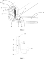
FIG. 2 is a schematic cross-sectional view of the display device inFIG. 1 in an I-I direction; -
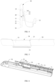
FIG. 3 is a schematic cross-sectional view of a fixing structure of a flexible printed circuit board and a drive board in a direction perpendicular to a length direction of the drive board according to an embodiment of this application; -
FIG. 4 is a schematic cross-sectional view of a fixing structure between a flexible printed circuit board and a drive board in a direction perpendicular to a length direction of the drive board according to another embodiment of this application; -
FIG. 5 is a schematic front view of a fixing structure between a flexible printed circuit board and a drive board according to an embodiment of this application; -
FIG. 6 is a schematic structural diagram of an accommodating cavity of the protrusion according to an embodiment of this application; and -
FIG. 7 is a schematic structural diagram of a display device according to another embodiment of this application. - The following clearly and completely describes the technical solutions in the embodiments of this application with reference to the accompanying drawings in the embodiments of this application.
- This application provides a display device on which a narrow bezel can be implemented. The display device may be a notebook computer, or may be a display device such as a television or a tablet computer.
- Referring to
FIG. 1 andFIG. 2 , this embodiment provides a display device. The display device includes adisplay part 100. Thedisplay part 100 includes adisplay panel 10, adrive board 20, and a flexible printedcircuit board 30 electrically connected to thedisplay panel 10 and thedrive board 20. Thedrive board 20 provides a drive signal for thedisplay panel 10 by using the flexible printedcircuit board 30, to drive thedisplay panel 10 to perform display. Abezel 40 is disposed around thedisplay panel 10. On one side of thedisplay panel 10, thebezel 40 protrudes from a surface on which thedisplay panel 10 is located to form aprotrusion 50. In this embodiment, thedisplay panel 10 is a quadrilateral panel and includes four side edges. Thebezel 40 includes anupper bezel 41, alower bezel 42 opposite to theupper bezel 41, and aleft bezel 43 and aright bezel 44 located between theupper bezel 41 and thelower bezel 42. Theupper bezel 41, thelower bezel 42, theleft bezel 43, and theright bezel 44 are separately located on sides at the four side edges of thedisplay panel 10. In this embodiment, thelower bezel 42 protrudes from the surface on which thedisplay panel 10 is located to form theprotrusion 50. Anaccommodating cavity 51 is formed in theprotrusion 50. Thedrive board 20 is fixed in theaccommodating cavity 51, and thedrive board 20 and thedisplay panel 10 are disposed at an included angle. That thedrive board 20 and thedisplay panel 10 are disposed at an included angle means that thedrive board 20 and thedisplay panel 10 are disposed at a specific included angle. - The
drive board 20 is disposed in theaccommodating cavity 51 of theprotrusion 50 that protrudes from a plane on which thedisplay panel 10 is located, so that thedrive board 20 and thedisplay panel 10 can be disposed at the included angle. Therefore, a projection of thedrive board 20 on the plane on which thedisplay panel 10 is located is reduced, and a width of thebezel 40 used to cover thedrive board 20 can be reduced. - Referring to
FIG. 2 and FIG. 3 , thedrive board 20 includes afront facet 21 and aback facet 22 opposite to thefront facet 21. In this embodiment, thedrive board 20 is a PCB. It can be understood that the PCB board may be a single-sided PCB board, or may be a double-sided PCB or a multi-layer PCB. In this embodiment, thedrive board 20 is a single-sided PCB, and a connection line is disposed on the front facet of thedrive board 20. The flexible printedcircuit board 30 includes afirst end 31 fixed to thefront facet 21 of thedrive board 20, asecond end 32 connected to thedisplay panel 10, and a fixedsection 33 located between thefirst end 31 and thesecond end 32. The fixedsection 33 is fixed to theback facet 22 of thedrive board 20. Specifically, thefirst end 31 of the flexible printedcircuit board 30 is fixed to thefront facet 21 and is electrically connected to the connection line on thefront facet 21, to provide a display signal for thedisplay panel 10 through the connection line. The flexible printedcircuit board 30 extends from thefront facet 21 to theback facet 22 through a side facet of thedrive board 20, and the fixedsection 33 is fixed to theback facet 22, so that when the flexible printedcircuit board 30 is subsequently pulled, a force-bearing location on the flexible printedcircuit board 30 is the fixedsection 33, and thefirst end 31 is not pulled, thereby preventing thefirst end 31 from being detached from thedrive board 20 due to pulling. - Manners of fixing the fixed
section 33 to theback facet 22 include but are not limited to fixing by using bonding glue such as an adhesive, clamping, and other fixing manners. Referring toFIG. 3 , in an embodiment of this application, the fixedsection 33 is fixed to theback facet 22 by using an adhesive 34. Thedrive board 20 includes abottom facet 24 and atop facet 25 that are connected to thefront facet 21 and theback facet 22 and that are disposed opposite to each other. Thebottom facet 24 is close to thedisplay panel 10. The flexible printedcircuit board 30 extends from thefront facet 21 to theback facet 22 through thetop facet 25. A thickness of the adhesive 34 gradually increases in a direction from thetop facet 25 to thebottom facet 24. The thickness of the adhesive gradually increases in the direction from thetop facet 25 to thebottom facet 24, so that a specific angle is formed between the fixedsection 33 and theback facet 22, to increase an angle formed by bending a section between thesecond end 32 and the fixedsection 33 of the flexible printedcircuit board 30. Therefore, a bending degree of the flexible printedcircuit board 30 can be further reduced, thereby avoiding damage to the flexible printedcircuit board 30 due to an excessively large bending degree of the flexible printedcircuit board 30. - Referring to
FIG. 4 , in some embodiments of this application, the adhesive 34 may include a plurality of sub-areas 341 disposed at intervals in the direction from thetop facet 25 to thebottom facet 24. The plurality of sub-areas 341 are used to fix the fixedsection 33 at a plurality of points, to achieve a better fixing effect. In addition, a section, between adjacent sub-areas 341, of the fixedsection 33 is curved, so that when one fixing point is detached, the curved fixedsection 33 can provide stretching space to avoid further detaching of another fixing point, to achieve a better fixing effect. - Referring to
FIG. 5 , in some embodiments of this application, agroove 23 is provided at a side edge of thedrive board 20, and a section between thefirst end 31 and the fixedsection 33 of the flexible printedcircuit board 30 extends from thefront facet 21 to theback facet 22 through thegroove 23. Thegroove 23 is provided at the side edge of thedrive board 20, and the flexible printedcircuit board 30 extends to theback facet 22 through thegroove 23, so that the flexible printedcircuit board 30 does not protrude at an edge of the flexible printedcircuit board 30 when bypassing thedrive board 20, thereby avoiding damage caused to the flexible printedcircuit board 30 by an inner wall of theaccommodating cavity 51 when thedrive board 20 is fixed in theaccommodating cavity 51. - Further, in some embodiments, a length of the
groove 23 is the same as a width of the flexible printedcircuit board 30, so that when the flexible printedcircuit board 30 extends to theback facet 22 through thegroove 23, the flexible printedcircuit board 30 is properly clamped in thegroove 23. This avoids a case in which a portion between thefirst end 31 and the fixedsection 33 moves along a length direction of thedrive board 20 and therefore thefirst end 31 is detached from thedrive board 20. The length direction of thedrive board 20 is the same as a length direction of an edge, corresponding to thelower bezel 42, of the display panel. - In some other embodiments of this application, a fixing structure such as an adhesive may be disposed in the
groove 23, so that a part of the flexible printedcircuit board 30 is fixed in thegroove 23, thereby further avoiding detaching between thefirst end 31 and thefront facet 21 when the flexible printedcircuit board 30 is pulled. - In some other embodiments of this application, a through-hole is provided on the
drive board 20, and a section between thefirst end 31 and the fixedsection 33 of the flexible printedcircuit board 30 passes the through-hole to extend to theback facet 22, so that a length of the flexible printedcircuit board 30 can be shortened. In addition, the flexible printedcircuit board 30 can be prevented from protruding at an edge of the flexible printedcircuit board 30 when bypassing thedrive board 20, thereby avoiding damage caused to the flexible printedcircuit board 30 by an inner wall of theaccommodating cavity 51 when thedrive board 20 is fixed in theaccommodating cavity 51. In an embodiment, a length direction of the through-hole is the same as a length direction of thedrive board 20, and a length of the through-hole is the same as a width of the flexible printedcircuit board 30, so that when the flexible printedcircuit board 30 extends to theback facet 22 through the through-hole, the flexible printedcircuit board 30 is properly clamped in the through-hole. This avoids a case in which a portion between thefirst end 31 and the fixedsection 33 moves along the length direction of thedrive board 20 and therefore thefirst end 31 is detached from thedrive board 20. - Further, still referring to
FIG. 2 to FIG. 4 , in some embodiments of this application, a section between the fixedsection 33 and thesecond end 32 of the flexible printedcircuit board 30 is curved, so that a length of the flexible printedcircuit board 30 between thedrive board 20 and thedisplay panel 10 is greater than a distance between thedrive board 20 and thedisplay panel 10, and the flexible printedcircuit board 30 has specific stretching space, thereby avoiding damage to the flexible printedcircuit board 30 due to pulling in a process in which the flexible printedcircuit board 30 is electrically connected to thedrive board 20 and thedisplay panel 10. - In some embodiments of this application, the included angle between the
drive board 20 and thedisplay panel 10 is greater than or equal to 90°, to minimize the projection of thedrive board 20 on the plane on which thedisplay panel 10 is located, and minimize the width of thebezel 40. In addition, the included angle between thedrive board 20 and thedisplay panel 10 is greater than or equal to 90°, so that an angle formed by bending the section between the fixedsection 33 and thesecond end 32 of the flexible printedcircuit board 30 is greater than or equal to 90°, thereby avoiding damage to the flexible printedcircuit board 30 due to an excessively large bending degree of the flexible printedcircuit board 30. Preferably, the included angle between thedrive board 20 and thedisplay panel 10 is 90°, so that the width of thebezel 40 is minimized. - Further, referring to
FIG. 6 , in some embodiments of this application, abuffer piece 60 is disposed between thedrive board 20 and an inner wall of theprotrusion 50. Thebuffer piece 60 provides buffering between thedrive board 20 and the inner wall of theprotrusion 50, to avoid collision between thedrive board 20 and the inner wall of theprotrusion 50 when thedisplay device 100 encounters collision, and therefore avoid damage to thedrive board 20. In some embodiments of this application, there are a plurality ofbuffer pieces 60, and the plurality ofbuffer pieces 60 are disposed at intervals along the length direction of thedrive board 20, to support thedrive board 20 at a plurality of points, so that a comparatively good heat dissipation effect can be achieved while buffering is implemented between thedrive board 20 and the inner wall of theprotrusion 50. In this embodiment, thebuffer piece 60 may be a rubber piece. Thebuffer piece 60 is fixed on the inner wall of theprotrusion 50. After thedrive board 20 is fixed in the accommodating cavity of theprotrusion 50, thebuffer piece 60 abuts against thefront facet 21 and theback facet 22 of thedrive board 20. - Further, in some embodiments of this application, the
protrusion 50 is made of a signal shielding material, or a shield layer is disposed on the inner wall or an outer wall of theprotrusion 50, to shield an external signal by using theprotrusion 50, and avoid interference from the external signal to a signal transmitted by thedrive board 20. In this embodiment, theprotrusion 50 is made of a plastic material, and the inner wall of theprotrusion 50 is coated with a metal shield layer, to shield an external signal. - Referring to
FIG. 2 andFIG. 6 , thedisplay device 100 further includes abackplane 70, and the outer wall of theprotrusion 50 is detachably fixed to thebackplane 70. Theprotrusion 50 includes afirst housing 52 and asecond housing 53 that are detachably connected. Thefirst housing 52 and thesecond housing 53 are detachably fixed on thebackplane 70. Thefirst housing 52, thesecond housing 53, and thebackplane 70 enclose theaccommodating cavity 51. Specifically, thefirst housing 52 may be connected to thesecond housing 53 in a detachable fixing manner, for example, fixing by using a clip or fixing by using a screw. Theprotrusion 50 is disposed as thefirst housing 52 and thesecond housing 53 that are detachably connected. During installation of thedrive board 20, thefirst housing 52 can be first fixed on thebackplane 70, then thedrive board 20 is fixed, and finally thesecond housing 53 is fixed to thefirst housing 52, so that thedrive board 20 is fixed in theaccommodating cavity 51 of theprotrusion 50. In other words, theprotrusion 50 is disposed as a structure formed by connecting thefirst housing 52 and thesecond housing 53, so that thedrive board 20 can be conveniently installed in theaccommodating cavity 51 and connected to thedisplay panel 10, and thedrive board 20 can be conveniently replaced or repaired. - Specifically, still referring to
FIG. 6 , in an embodiment of this application, afront retaining wall 71 and arear retaining wall 72 spaced apart from thefront retaining wall 71 are disposed at a location that is on thebackplane 70 and that corresponds to theprotrusion 50, and a side that is of thedrive board 20 and that faces thebackplane 70 is sandwiched between thefront retaining wall 71 and therear retaining wall 72. Specifically, thefront retaining wall 71 and therear retaining wall 72 are protruding columns that protrude from an inner surface of thebackplane 70, and there are a plurality offront retaining walls 71 andrear retaining walls 72. The plurality offront retaining walls 71 are located on a side of thefront facet 21 of thedrive board 20 and are disposed at intervals along the length direction of thedrive board 20. The plurality ofrear retaining walls 72 are located on a side of theback facet 22 of thedrive board 20 and are disposed at intervals along the length direction of thedrive board 20. Thedrive board 20 is sandwiched between the plurality offront retaining walls 71 and the plurality ofrear retaining walls 72, so that all locations on thedrive board 20 can be properly fixed to thebackplane 70. Further, ahook 521 protrudes on thefirst housing 52, and a side that is of thedrive board 20 and that is away from thebackplane 70 is fixed to thefirst housing 52 by using thehook 521. Thedrive board 20 is fixed in theaccommodating cavity 51 of theprotrusion 50 by using the hook on thefirst housing 52 and by using thefront retaining wall 71 and therear retaining wall 72 on thebackplane 70. Finally, thesecond housing 53 is fixed to thefirst housing 52, to keep theaccommodating cavity 51 sealed, and prevent external impurities from entering theaccommodating cavity 51. - Further,
support ribs 54 are disposed on inner walls of thefirst housing 52 and thesecond housing 53. Thesupport rib 54 of thefirst housing 52 abuts against thefront facet 21 of thedrive board 20. Thesupport rib 54 of thesecond housing 53 abuts against theback facet 22 of thedrive board 20. There are a plurality ofsupport ribs 54 on each of the inner walls of thefirst housing 52 and thesecond housing 53. The plurality ofsupport ribs 54 are disposed at intervals along the length direction of thedrive board 20, to support all locations on thedrive board 20 by using thesupport ribs 54 on the inner walls of thefirst housing 52 and thesecond housing 53, and ensure stability of thedrive board 20 in theaccommodating cavity 51. - Further, referring to
FIG. 7 , in some embodiments of this application, thedisplay device 100 includes arotating shaft 80, the rotatingshaft 80 is accommodated in theprotrusion 50, and two ends of theprotrusion 50 extend out of theprotrusion 50. The rotatingshaft 80 is disposed in theprotrusion 50, so that a structure of the display device is simplified. For a display device with a rotating shaft structure, such as a notebook computer, theprotrusion 50 is a rotating shaft cover of a mounting rotating shaft in the current technology. In this application, thedrive board 20 is disposed in the rotating shaft cover, to reduce the bezel of the display device without increasing the structure of the display device. It can be understood that, in another embodiment of this application, when the display device is a display device without a rotating shaft, such as a television or a tablet computer, theprotrusion 50 may be a structure such as a television base, or theprotrusion 50 is formed by protruding, by a location that is on the backplane and that corresponds to the lower bezel, from a plane on which the backplane is located, so that the display device has good appearance. - Further, the display device further includes a functional part, the rotating
shaft 80 is connected to thedisplay part 100 and the functional part, so that thedisplay part 100 and the functional part are rotatably connected. The rotatingshaft 80 is rotatably connected to thedisplay part 100 and the functional part, so that thedisplay part 100 and the functional part can be folded relative to each other, thereby extending a use function of the display device. For example, when the display device is a notebook computer, the functional part is a keyboard of the notebook computer. - The foregoing descriptions are merely preferred implementations of this application. It should be noted that a person of ordinary skill in the art may make several improvements or polishing without departing from the principle of this application and the improvements or polishing shall fall within the protection scope as defined in the appended claims.
Claims (13)
- A display device, comprising a display part (100), wherein the display part (100) comprises a display panel (10), a bezel (40), a drive board (20), and a flexible printed circuit board (30) electrically connected to the display panel (10) and the drive board (20), the bezel (40) is located on one side of the display panel (10) and protrudes relative to a surface on which the display panel (10) is located, an accommodating cavity (51) is provided in the bezel (40), the drive board (20) is fixed in the accommodating cavity (51), and the drive board (20) and the display panel (10) are disposed at an included angle; and the drive board (20) comprises a front facet (21) on which a connection line is disposed and a back facet (22), the flexible printed circuit board (30) comprises a first end (31) and a second end (32), wherein the second end (32) is fixedly connected to the display panel (10), and the first end (31) is fixed to the front facet (21), the first end (31) is away from the display panel (10),
characterized in thatthe flexible printed circuit board (30) comprises a fixed section (33) located between the first end (31) and the second end (32),the fixed section (33) faces the display panel (10), andthe fixed section (33) is fixed to the back facet (22). - The display device according to claim 1, wherein a section between the fixed section (33) and the second end (32) is curved.
- The display device according to claim 1, wherein the included angle between the drive board (20) and the display panel (10) is greater than or equal to 90°.
- The display device according to any one of claims 1 to 3, wherein the fixed section (33) is fixed to the back facet (22) by using an adhesive (34), the drive board (20) comprises a bottom facet (24) and a top facet (25) that are connected to the front facet (21) and the back facet (22) and that are disposed opposite to each other, the bottom facet (24) is close to the display panel (10), the flexible printed circuit board (30) extends from the front facet (21) to the back facet (22) through the top facet (25), and a thickness of the adhesive (34) gradually increases in a direction from the top facet (25) to the bottom facet (24).
- The display device according to claim 4, wherein the adhesive (34) comprises a plurality of sub-areas (341) disposed at intervals in the direction from the top facet (25) to the bottom facet (24).
- The display device according to claim 1, wherein the drive board (20) comprises a bottom facet (24) and a top facet (25) that are connected to the front facet (21) and the back facet (22) and that are disposed opposite to each other, the bottom facet (24) is close to the display panel (10), a groove is recessed on the top facet (25) in a direction towards the bottom facet (24), and a part of the flexible printed circuit board (30) is accommodated in the groove.
- The display device according to claim 1, wherein a through-hole is provided on the drive board (20), and a section between the first end (31) and the fixed section (33) of the flexible printed circuit board (30) passes the through-hole to extend to the back facet (22).
- The display device according to claim 1, wherein a buffer piece (60) is disposed between the drive board (20) and an inner wall of the bezel (40).
- The display device according to claim 1, wherein the bezel (40) is made of a signal shielding material, or a shielded layer is disposed on the inner wall or an outer wall of the bezel (40).
- The display device according to claim 1, wherein the display device comprises a backplane (70), the bezel (40) protrudes relative to the surface on which the display panel (10) is located to form a protrusion (50), the protrusion (50) comprises a first housing (52) and a second housing (53), the first housing (52) and the second housing (53) are detachably fixed on the backplane (70), and the first housing (52), the second housing (53), and the backplane (70) enclose the accommodating cavity (51).
- The display device according to claim 10, wherein a front retaining wall (71) and a rear retaining wall (72) spaced apart from the front retaining wall (71) are disposed on the backplane (70), a side that is of the drive board (20) and that faces the backplane (70) is sandwiched between the front retaining wall (71) and the rear retaining wall (72), a hook (521) protrudes on the first housing (52), and a side that is of the drive board (20) and that is away from the backplane (70) is fixed to the first housing (52) by using the hook (521).
- The display device according to claim 11, wherein support ribs (54) are disposed on inner walls of the first housing (52) and the second housing (53), the support rib (54) of the first housing (52) abuts against the front facet (21) of the drive board (20), and the support rib (54) of the second housing (53) abuts against the back facet (22) of the drive board (20).
- The display device according to claim 1, wherein the display device comprises a rotating shaft (80) and a functional part, the rotating shaft (80) is accommodated in the accommodating cavity (51), and the rotating shaft (80) is connected to the display part (100) and the functional part, so that the display part (100) and the functional part are rotatably connected.
Applications Claiming Priority (2)
| Application Number | Priority Date | Filing Date | Title |
|---|---|---|---|
| CN201811315970.5A CN109493723B (en) | 2018-11-06 | 2018-11-06 | display screen |
| PCT/CN2019/108592 WO2020093814A1 (en) | 2018-11-06 | 2019-09-27 | Display device |
Publications (3)
| Publication Number | Publication Date |
|---|---|
| EP3855415A1 EP3855415A1 (en) | 2021-07-28 |
| EP3855415A4 EP3855415A4 (en) | 2021-11-10 |
| EP3855415B1 true EP3855415B1 (en) | 2023-06-14 |
Family
ID=65694036
Family Applications (1)
| Application Number | Title | Priority Date | Filing Date |
|---|---|---|---|
| EP19881855.1A Active EP3855415B1 (en) | 2018-11-06 | 2019-09-27 | Display device |
Country Status (4)
| Country | Link |
|---|---|
| US (1) | US11785725B2 (en) |
| EP (1) | EP3855415B1 (en) |
| CN (1) | CN109493723B (en) |
| WO (1) | WO2020093814A1 (en) |
Families Citing this family (13)
| Publication number | Priority date | Publication date | Assignee | Title |
|---|---|---|---|---|
| CN109493723B (en) | 2018-11-06 | 2020-09-04 | 华为技术有限公司 | display screen |
| TWI724807B (en) * | 2019-07-24 | 2021-04-11 | 友達光電股份有限公司 | Flexible apparatus |
| CN110580084B (en) | 2019-08-06 | 2021-10-15 | 华为技术有限公司 | a mobile terminal |
| CN111857247A (en) * | 2020-07-07 | 2020-10-30 | 北京小米移动软件有限公司 | Display modules and electronic equipment |
| CN113376888A (en) * | 2021-07-12 | 2021-09-10 | 合肥京东方光电科技有限公司 | Display device |
| CN113803362B (en) * | 2021-09-16 | 2023-02-03 | 东莞华贝电子科技有限公司 | Rotating shaft cover and electronic equipment |
| CN116414189A (en) * | 2021-12-29 | 2023-07-11 | 华为技术有限公司 | A foldable terminal |
| CN116056374B (en) * | 2022-06-10 | 2023-11-10 | 荣耀终端有限公司 | Middle frame for electronic equipment and electronic equipment |
| CN115206191B (en) * | 2022-07-13 | 2023-10-31 | 武汉华星光电半导体显示技术有限公司 | Electronic equipment |
| US12585421B2 (en) | 2022-12-14 | 2026-03-24 | Dell Products L.P. | Information handling system keyboard membrane with speaker interface |
| US12560976B2 (en) * | 2022-12-14 | 2026-02-24 | Dell Products L.P. | Information handling system security lock and keystone housing assembly |
| CN116794868A (en) * | 2023-07-31 | 2023-09-22 | 合肥京东方光电科技有限公司 | Display module and display device |
| CN117253421B (en) * | 2023-09-26 | 2026-02-13 | 厦门天马微电子有限公司 | Display modules and display devices |
Family Cites Families (22)
| Publication number | Priority date | Publication date | Assignee | Title |
|---|---|---|---|---|
| TWI228616B (en) * | 1999-11-30 | 2005-03-01 | Samsung Electronics Co Ltd | Liquid crystal display device |
| JP3788972B2 (en) * | 2003-01-15 | 2006-06-21 | 株式会社東芝 | Display device |
| JP5148059B2 (en) * | 2005-11-07 | 2013-02-20 | 株式会社ジャパンディスプレイセントラル | Liquid crystal display |
| JP5026690B2 (en) * | 2005-11-21 | 2012-09-12 | 株式会社ジャパンディスプレイイースト | Display device |
| JP2012123170A (en) * | 2010-12-08 | 2012-06-28 | Sony Corp | Display device |
| JP5021102B1 (en) * | 2011-09-30 | 2012-09-05 | シャープ株式会社 | Liquid crystal display |
| WO2013089030A1 (en) | 2011-12-16 | 2013-06-20 | シャープ株式会社 | Display device, and television reception device |
| JP2013174705A (en) * | 2012-02-24 | 2013-09-05 | Sharp Corp | Display unit and television receiver |
| KR101366539B1 (en) * | 2012-04-30 | 2014-02-25 | 엘지디스플레이 주식회사 | Image display device and method of fabricating the same |
| CN103018937B (en) | 2012-12-26 | 2015-08-19 | 深圳市华星光电技术有限公司 | Narrow frame liquid crystal module |
| WO2015063883A1 (en) * | 2013-10-30 | 2015-05-07 | 堺ディスプレイプロダクト株式会社 | Display device |
| KR102354928B1 (en) * | 2015-08-31 | 2022-01-21 | 엘지디스플레이 주식회사 | Side cover film for display and display device comprising the same |
| CN205091659U (en) | 2015-11-11 | 2016-03-16 | 合肥联宝信息技术有限公司 | Notebook computer's demonstration end and notebook computer thereof |
| KR102552047B1 (en) | 2016-11-24 | 2023-07-07 | 엘지디스플레이 주식회사 | Display device |
| CN106547140A (en) * | 2017-01-17 | 2017-03-29 | 青岛海信电器股份有限公司 | A kind of display floater and liquid crystal indicator |
| CN107193166A (en) * | 2017-06-06 | 2017-09-22 | 深圳天珑无线科技有限公司 | A kind of display device and its manufacture method |
| CN107195663B (en) | 2017-06-08 | 2020-09-01 | 深圳市华星光电半导体显示技术有限公司 | AMOLED display panel structure |
| CN207249549U (en) | 2017-09-18 | 2018-04-17 | 苏州三星电子电脑有限公司 | Laptop |
| CN207571656U (en) | 2017-12-28 | 2018-07-03 | 合肥联宝信息技术有限公司 | Display screen and electronic equipment |
| CN207676075U (en) * | 2018-01-05 | 2018-07-31 | 信利半导体有限公司 | A kind of liquid crystal display device |
| CN109493723B (en) | 2018-11-06 | 2020-09-04 | 华为技术有限公司 | display screen |
| CN110580084B (en) * | 2019-08-06 | 2021-10-15 | 华为技术有限公司 | a mobile terminal |
-
2018
- 2018-11-06 CN CN201811315970.5A patent/CN109493723B/en active Active
-
2019
- 2019-09-27 US US17/290,822 patent/US11785725B2/en active Active
- 2019-09-27 EP EP19881855.1A patent/EP3855415B1/en active Active
- 2019-09-27 WO PCT/CN2019/108592 patent/WO2020093814A1/en not_active Ceased
Also Published As
| Publication number | Publication date |
|---|---|
| CN109493723B (en) | 2020-09-04 |
| EP3855415A1 (en) | 2021-07-28 |
| US11785725B2 (en) | 2023-10-10 |
| US20220087035A1 (en) | 2022-03-17 |
| CN109493723A (en) | 2019-03-19 |
| WO2020093814A1 (en) | 2020-05-14 |
| EP3855415A4 (en) | 2021-11-10 |
Similar Documents
| Publication | Publication Date | Title |
|---|---|---|
| US11785725B2 (en) | Display device | |
| EP1833246A2 (en) | Display apparatus | |
| CN106409863B (en) | Display device | |
| TW201305667A (en) | Flat display | |
| CN104696826B (en) | Backlight module and display device | |
| CN210722258U (en) | Display device | |
| CN106598178A (en) | Interactive intelligent tablet | |
| US20160341886A1 (en) | Backlight module and display device | |
| CN102721011A (en) | Support member for supporting light guide plate, and backlight module, display module and display device using the same | |
| KR102227016B1 (en) | Display Device | |
| US12517552B2 (en) | Electronic apparatus including bezel and double sided tapes | |
| US10082620B2 (en) | Backlight module and display screen | |
| JP2015129862A (en) | Display device | |
| CN215181290U (en) | Back plate, backlight module and display device | |
| JP5883067B2 (en) | Image display device | |
| WO2017084196A1 (en) | Liquid crystal screen gate cof structural component and liquid crystal display device | |
| EP3582208B1 (en) | Image display apparatus | |
| CN106409162A (en) | Display device | |
| US20230247851A1 (en) | Electronic apparatus and panel body | |
| JP2009116072A (en) | Plasma display device | |
| US9122086B2 (en) | Display apparatus | |
| JP7607815B1 (en) | Electronics | |
| KR102239593B1 (en) | Display Device and Set Electronic Apparatus having the same | |
| CN203706174U (en) | Touch control display device | |
| JPH10142584A (en) | Liquid crystal display |
Legal Events
| Date | Code | Title | Description |
|---|---|---|---|
| STAA | Information on the status of an ep patent application or granted ep patent |
Free format text: STATUS: THE INTERNATIONAL PUBLICATION HAS BEEN MADE |
|
| PUAI | Public reference made under article 153(3) epc to a published international application that has entered the european phase |
Free format text: ORIGINAL CODE: 0009012 |
|
| STAA | Information on the status of an ep patent application or granted ep patent |
Free format text: STATUS: REQUEST FOR EXAMINATION WAS MADE |
|
| 17P | Request for examination filed |
Effective date: 20210421 |
|
| AK | Designated contracting states |
Kind code of ref document: A1 Designated state(s): AL AT BE BG CH CY CZ DE DK EE ES FI FR GB GR HR HU IE IS IT LI LT LU LV MC MK MT NL NO PL PT RO RS SE SI SK SM TR |
|
| A4 | Supplementary search report drawn up and despatched |
Effective date: 20211013 |
|
| RIC1 | Information provided on ipc code assigned before grant |
Ipc: G02F 1/1345 20060101ALI20211007BHEP Ipc: G02F 1/1333 20060101ALI20211007BHEP Ipc: G09F 9/00 20060101AFI20211007BHEP |
|
| DAV | Request for validation of the european patent (deleted) | ||
| DAX | Request for extension of the european patent (deleted) | ||
| GRAP | Despatch of communication of intention to grant a patent |
Free format text: ORIGINAL CODE: EPIDOSNIGR1 |
|
| STAA | Information on the status of an ep patent application or granted ep patent |
Free format text: STATUS: GRANT OF PATENT IS INTENDED |
|
| INTG | Intention to grant announced |
Effective date: 20230223 |
|
| GRAS | Grant fee paid |
Free format text: ORIGINAL CODE: EPIDOSNIGR3 |
|
| GRAA | (expected) grant |
Free format text: ORIGINAL CODE: 0009210 |
|
| STAA | Information on the status of an ep patent application or granted ep patent |
Free format text: STATUS: THE PATENT HAS BEEN GRANTED |
|
| AK | Designated contracting states |
Kind code of ref document: B1 Designated state(s): AL AT BE BG CH CY CZ DE DK EE ES FI FR GB GR HR HU IE IS IT LI LT LU LV MC MK MT NL NO PL PT RO RS SE SI SK SM TR |
|
| REG | Reference to a national code |
Ref country code: CH Ref legal event code: EP |
|
| REG | Reference to a national code |
Ref country code: DE Ref legal event code: R096 Ref document number: 602019031192 Country of ref document: DE |
|
| REG | Reference to a national code |
Ref country code: AT Ref legal event code: REF Ref document number: 1579797 Country of ref document: AT Kind code of ref document: T Effective date: 20230715 |
|
| REG | Reference to a national code |
Ref country code: LT Ref legal event code: MG9D |
|
| REG | Reference to a national code |
Ref country code: NL Ref legal event code: MP Effective date: 20230614 |
|
| PG25 | Lapsed in a contracting state [announced via postgrant information from national office to epo] |
Ref country code: SE Free format text: LAPSE BECAUSE OF FAILURE TO SUBMIT A TRANSLATION OF THE DESCRIPTION OR TO PAY THE FEE WITHIN THE PRESCRIBED TIME-LIMIT Effective date: 20230614 Ref country code: NO Free format text: LAPSE BECAUSE OF FAILURE TO SUBMIT A TRANSLATION OF THE DESCRIPTION OR TO PAY THE FEE WITHIN THE PRESCRIBED TIME-LIMIT Effective date: 20230914 Ref country code: ES Free format text: LAPSE BECAUSE OF FAILURE TO SUBMIT A TRANSLATION OF THE DESCRIPTION OR TO PAY THE FEE WITHIN THE PRESCRIBED TIME-LIMIT Effective date: 20230614 |
|
| REG | Reference to a national code |
Ref country code: AT Ref legal event code: MK05 Ref document number: 1579797 Country of ref document: AT Kind code of ref document: T Effective date: 20230614 |
|
| PG25 | Lapsed in a contracting state [announced via postgrant information from national office to epo] |
Ref country code: RS Free format text: LAPSE BECAUSE OF FAILURE TO SUBMIT A TRANSLATION OF THE DESCRIPTION OR TO PAY THE FEE WITHIN THE PRESCRIBED TIME-LIMIT Effective date: 20230614 Ref country code: NL Free format text: LAPSE BECAUSE OF FAILURE TO SUBMIT A TRANSLATION OF THE DESCRIPTION OR TO PAY THE FEE WITHIN THE PRESCRIBED TIME-LIMIT Effective date: 20230614 Ref country code: LV Free format text: LAPSE BECAUSE OF FAILURE TO SUBMIT A TRANSLATION OF THE DESCRIPTION OR TO PAY THE FEE WITHIN THE PRESCRIBED TIME-LIMIT Effective date: 20230614 Ref country code: LT Free format text: LAPSE BECAUSE OF FAILURE TO SUBMIT A TRANSLATION OF THE DESCRIPTION OR TO PAY THE FEE WITHIN THE PRESCRIBED TIME-LIMIT Effective date: 20230614 Ref country code: HR Free format text: LAPSE BECAUSE OF FAILURE TO SUBMIT A TRANSLATION OF THE DESCRIPTION OR TO PAY THE FEE WITHIN THE PRESCRIBED TIME-LIMIT Effective date: 20230614 Ref country code: GR Free format text: LAPSE BECAUSE OF FAILURE TO SUBMIT A TRANSLATION OF THE DESCRIPTION OR TO PAY THE FEE WITHIN THE PRESCRIBED TIME-LIMIT Effective date: 20230915 |
|
| PG25 | Lapsed in a contracting state [announced via postgrant information from national office to epo] |
Ref country code: FI Free format text: LAPSE BECAUSE OF FAILURE TO SUBMIT A TRANSLATION OF THE DESCRIPTION OR TO PAY THE FEE WITHIN THE PRESCRIBED TIME-LIMIT Effective date: 20230614 |
|
| PG25 | Lapsed in a contracting state [announced via postgrant information from national office to epo] |
Ref country code: SK Free format text: LAPSE BECAUSE OF FAILURE TO SUBMIT A TRANSLATION OF THE DESCRIPTION OR TO PAY THE FEE WITHIN THE PRESCRIBED TIME-LIMIT Effective date: 20230614 |
|
| PG25 | Lapsed in a contracting state [announced via postgrant information from national office to epo] |
Ref country code: IS Free format text: LAPSE BECAUSE OF FAILURE TO SUBMIT A TRANSLATION OF THE DESCRIPTION OR TO PAY THE FEE WITHIN THE PRESCRIBED TIME-LIMIT Effective date: 20231014 |
|
| PG25 | Lapsed in a contracting state [announced via postgrant information from national office to epo] |
Ref country code: SM Free format text: LAPSE BECAUSE OF FAILURE TO SUBMIT A TRANSLATION OF THE DESCRIPTION OR TO PAY THE FEE WITHIN THE PRESCRIBED TIME-LIMIT Effective date: 20230614 Ref country code: SK Free format text: LAPSE BECAUSE OF FAILURE TO SUBMIT A TRANSLATION OF THE DESCRIPTION OR TO PAY THE FEE WITHIN THE PRESCRIBED TIME-LIMIT Effective date: 20230614 Ref country code: RO Free format text: LAPSE BECAUSE OF FAILURE TO SUBMIT A TRANSLATION OF THE DESCRIPTION OR TO PAY THE FEE WITHIN THE PRESCRIBED TIME-LIMIT Effective date: 20230614 Ref country code: PT Free format text: LAPSE BECAUSE OF FAILURE TO SUBMIT A TRANSLATION OF THE DESCRIPTION OR TO PAY THE FEE WITHIN THE PRESCRIBED TIME-LIMIT Effective date: 20231016 Ref country code: IS Free format text: LAPSE BECAUSE OF FAILURE TO SUBMIT A TRANSLATION OF THE DESCRIPTION OR TO PAY THE FEE WITHIN THE PRESCRIBED TIME-LIMIT Effective date: 20231014 Ref country code: EE Free format text: LAPSE BECAUSE OF FAILURE TO SUBMIT A TRANSLATION OF THE DESCRIPTION OR TO PAY THE FEE WITHIN THE PRESCRIBED TIME-LIMIT Effective date: 20230614 Ref country code: CZ Free format text: LAPSE BECAUSE OF FAILURE TO SUBMIT A TRANSLATION OF THE DESCRIPTION OR TO PAY THE FEE WITHIN THE PRESCRIBED TIME-LIMIT Effective date: 20230614 Ref country code: AT Free format text: LAPSE BECAUSE OF FAILURE TO SUBMIT A TRANSLATION OF THE DESCRIPTION OR TO PAY THE FEE WITHIN THE PRESCRIBED TIME-LIMIT Effective date: 20230614 |
|
| PG25 | Lapsed in a contracting state [announced via postgrant information from national office to epo] |
Ref country code: PL Free format text: LAPSE BECAUSE OF FAILURE TO SUBMIT A TRANSLATION OF THE DESCRIPTION OR TO PAY THE FEE WITHIN THE PRESCRIBED TIME-LIMIT Effective date: 20230614 |
|
| REG | Reference to a national code |
Ref country code: DE Ref legal event code: R097 Ref document number: 602019031192 Country of ref document: DE |
|
| PLBE | No opposition filed within time limit |
Free format text: ORIGINAL CODE: 0009261 |
|
| STAA | Information on the status of an ep patent application or granted ep patent |
Free format text: STATUS: NO OPPOSITION FILED WITHIN TIME LIMIT |
|
| PG25 | Lapsed in a contracting state [announced via postgrant information from national office to epo] |
Ref country code: DK Free format text: LAPSE BECAUSE OF FAILURE TO SUBMIT A TRANSLATION OF THE DESCRIPTION OR TO PAY THE FEE WITHIN THE PRESCRIBED TIME-LIMIT Effective date: 20230614 |
|
| REG | Reference to a national code |
Ref country code: CH Ref legal event code: PL |
|
| PG25 | Lapsed in a contracting state [announced via postgrant information from national office to epo] |
Ref country code: SI Free format text: LAPSE BECAUSE OF FAILURE TO SUBMIT A TRANSLATION OF THE DESCRIPTION OR TO PAY THE FEE WITHIN THE PRESCRIBED TIME-LIMIT Effective date: 20230614 |
|
| PG25 | Lapsed in a contracting state [announced via postgrant information from national office to epo] |
Ref country code: LU Free format text: LAPSE BECAUSE OF NON-PAYMENT OF DUE FEES Effective date: 20230927 |
|
| 26N | No opposition filed |
Effective date: 20240315 |
|
| REG | Reference to a national code |
Ref country code: BE Ref legal event code: MM Effective date: 20230930 |
|
| GBPC | Gb: european patent ceased through non-payment of renewal fee |
Effective date: 20230927 |
|
| PG25 | Lapsed in a contracting state [announced via postgrant information from national office to epo] |
Ref country code: SI Free format text: LAPSE BECAUSE OF FAILURE TO SUBMIT A TRANSLATION OF THE DESCRIPTION OR TO PAY THE FEE WITHIN THE PRESCRIBED TIME-LIMIT Effective date: 20230614 Ref country code: LU Free format text: LAPSE BECAUSE OF NON-PAYMENT OF DUE FEES Effective date: 20230927 Ref country code: IT Free format text: LAPSE BECAUSE OF FAILURE TO SUBMIT A TRANSLATION OF THE DESCRIPTION OR TO PAY THE FEE WITHIN THE PRESCRIBED TIME-LIMIT Effective date: 20230614 Ref country code: MC Free format text: LAPSE BECAUSE OF FAILURE TO SUBMIT A TRANSLATION OF THE DESCRIPTION OR TO PAY THE FEE WITHIN THE PRESCRIBED TIME-LIMIT Effective date: 20230614 |
|
| REG | Reference to a national code |
Ref country code: IE Ref legal event code: MM4A |
|
| PG25 | Lapsed in a contracting state [announced via postgrant information from national office to epo] |
Ref country code: IE Free format text: LAPSE BECAUSE OF NON-PAYMENT OF DUE FEES Effective date: 20230927 |
|
| PG25 | Lapsed in a contracting state [announced via postgrant information from national office to epo] |
Ref country code: GB Free format text: LAPSE BECAUSE OF NON-PAYMENT OF DUE FEES Effective date: 20230927 |
|
| PG25 | Lapsed in a contracting state [announced via postgrant information from national office to epo] |
Ref country code: CH Free format text: LAPSE BECAUSE OF NON-PAYMENT OF DUE FEES Effective date: 20230930 |
|
| PG25 | Lapsed in a contracting state [announced via postgrant information from national office to epo] |
Ref country code: IE Free format text: LAPSE BECAUSE OF NON-PAYMENT OF DUE FEES Effective date: 20230927 Ref country code: GB Free format text: LAPSE BECAUSE OF NON-PAYMENT OF DUE FEES Effective date: 20230927 Ref country code: CH Free format text: LAPSE BECAUSE OF NON-PAYMENT OF DUE FEES Effective date: 20230930 |
|
| PG25 | Lapsed in a contracting state [announced via postgrant information from national office to epo] |
Ref country code: BE Free format text: LAPSE BECAUSE OF NON-PAYMENT OF DUE FEES Effective date: 20230930 |
|
| PG25 | Lapsed in a contracting state [announced via postgrant information from national office to epo] |
Ref country code: BG Free format text: LAPSE BECAUSE OF FAILURE TO SUBMIT A TRANSLATION OF THE DESCRIPTION OR TO PAY THE FEE WITHIN THE PRESCRIBED TIME-LIMIT Effective date: 20230614 |
|
| PG25 | Lapsed in a contracting state [announced via postgrant information from national office to epo] |
Ref country code: BG Free format text: LAPSE BECAUSE OF FAILURE TO SUBMIT A TRANSLATION OF THE DESCRIPTION OR TO PAY THE FEE WITHIN THE PRESCRIBED TIME-LIMIT Effective date: 20230614 |
|
| PG25 | Lapsed in a contracting state [announced via postgrant information from national office to epo] |
Ref country code: CY Free format text: LAPSE BECAUSE OF FAILURE TO SUBMIT A TRANSLATION OF THE DESCRIPTION OR TO PAY THE FEE WITHIN THE PRESCRIBED TIME-LIMIT; INVALID AB INITIO Effective date: 20190927 |
|
| PG25 | Lapsed in a contracting state [announced via postgrant information from national office to epo] |
Ref country code: HU Free format text: LAPSE BECAUSE OF FAILURE TO SUBMIT A TRANSLATION OF THE DESCRIPTION OR TO PAY THE FEE WITHIN THE PRESCRIBED TIME-LIMIT; INVALID AB INITIO Effective date: 20190927 |
|
| PGFP | Annual fee paid to national office [announced via postgrant information from national office to epo] |
Ref country code: DE Payment date: 20250805 Year of fee payment: 7 |
|
| PGFP | Annual fee paid to national office [announced via postgrant information from national office to epo] |
Ref country code: FR Payment date: 20250808 Year of fee payment: 7 |
|
| PG25 | Lapsed in a contracting state [announced via postgrant information from national office to epo] |
Ref country code: TR Free format text: LAPSE BECAUSE OF FAILURE TO SUBMIT A TRANSLATION OF THE DESCRIPTION OR TO PAY THE FEE WITHIN THE PRESCRIBED TIME-LIMIT Effective date: 20230614 |