EP3852271A1 - Io analog rail control circuit for power ramps - Google Patents
Io analog rail control circuit for power ramps Download PDFInfo
- Publication number
- EP3852271A1 EP3852271A1 EP20216729.2A EP20216729A EP3852271A1 EP 3852271 A1 EP3852271 A1 EP 3852271A1 EP 20216729 A EP20216729 A EP 20216729A EP 3852271 A1 EP3852271 A1 EP 3852271A1
- Authority
- EP
- European Patent Office
- Prior art keywords
- supply voltage
- vddio
- output
- voltage
- buffers
- Prior art date
- Legal status (The legal status is an assumption and is not a legal conclusion. Google has not performed a legal analysis and makes no representation as to the accuracy of the status listed.)
- Granted
Links
Images




Classifications
-
- H—ELECTRICITY
- H03—ELECTRONIC CIRCUITRY
- H03K—PULSE TECHNIQUE
- H03K19/00—Logic circuits, i.e. having at least two inputs acting on one output; Inverting circuits
- H03K19/0175—Coupling arrangements; Interface arrangements
- H03K19/0185—Coupling arrangements; Interface arrangements using field effect transistors only
- H03K19/018585—Coupling arrangements; Interface arrangements using field effect transistors only programmable
-
- H—ELECTRICITY
- H03—ELECTRONIC CIRCUITRY
- H03K—PULSE TECHNIQUE
- H03K19/00—Logic circuits, i.e. having at least two inputs acting on one output; Inverting circuits
- H03K19/003—Modifications for increasing the reliability for protection
- H03K19/00369—Modifications for compensating variations of temperature, supply voltage or other physical parameters
- H03K19/00384—Modifications for compensating variations of temperature, supply voltage or other physical parameters in field effect transistor circuits
-
- H—ELECTRICITY
- H03—ELECTRONIC CIRCUITRY
- H03K—PULSE TECHNIQUE
- H03K19/00—Logic circuits, i.e. having at least two inputs acting on one output; Inverting circuits
- H03K19/0175—Coupling arrangements; Interface arrangements
- H03K19/0185—Coupling arrangements; Interface arrangements using field effect transistors only
- H03K19/018507—Interface arrangements
- H03K19/018521—Interface arrangements of complementary type, e.g. CMOS
Landscapes
- Engineering & Computer Science (AREA)
- Computer Hardware Design (AREA)
- Physics & Mathematics (AREA)
- Computing Systems (AREA)
- General Engineering & Computer Science (AREA)
- Mathematical Physics (AREA)
- Logic Circuits (AREA)
- Semiconductor Integrated Circuits (AREA)
Abstract
Description
- Integrated circuits (ICs) such as System on Chips (SoCs), microcontrollers (MCUs), etc., communicate with external components such as dynamic random access memory (DRAM), dual data rate (DDR) memory, etc., through input output (I/O) buffers. Generally I/O buffers have input interfaces for communicating with internal core circuits (e.g., a central processing unit) of the IC, and output interfaces for communicating with components external to the IC via I/O pads. The input and output interfaces typically operate in different voltage domains.
- Metal oxide field effect transistors (MOSFETs) can be damaged if the gate to source (Vgs) or gate to drain (Vgd) voltage exceeds a maximum value TrMax. As semiconductor technology advances, and transistor size reduces, TrMax also reduces. Unfortunately the output interfaces of I/O buffers in modern ICs are often required to operate with an output supply voltage Vddio that exceeds TrMax. Protection MOSFETs can be added to I/O buffers to ensure reliable operation at high output supply voltages Vddio (e.g., Vddio = 3.3V). The gates of these protection MOSFETs, however, must be carefully biased, especially during power ramp up.
- The present technology may be better understood, and its numerous objects, features, and advantages made apparent to those skilled in the art by referencing the accompanying drawings.
-
Figure 1 is a block diagram that illustrates an example IC that includes power management circuit (PMC). -
Figure 2 is a mixed schematic and block diagram illustrating an example I/O buffer employed in the IC ofFigure 1 . -
Figure 3 is a block diagram that illustrates an example IC that lacks a PMC. -
Figure 4 is a mixed schematic and block diagram illustrating an example I/O buffer that can be employed in the IC ofFigure 3 . -
Figure 5 is a mixed schematic and block diagram illustrating an example of another I/O buffer that can be employed in the IC ofFigure 3 . -
Figure 6 is a block diagram illustrating an example buffer controller that can be employed in IC ofFigure 3 . -
Figure 7 is a block diagram illustrating one embodiment of a programmable bias voltage generator that can be employed in the buffer controller ofFigure 6 . -
Figure 8 is a schematic diagram of an example split level shifter that can be employed within the programmable bias voltage generator ofFigure 7 . -
Figure 9 is a schematic diagram of an example I/O bias voltage generator that can be employed in device ofFigure 7 . -
Figure 10 is a block diagram illustrating another example buffer controller that can be employed in IC ofFigure 3 . -
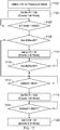
Figure 11 illustrates relevant aspects of the process employed by a supply voltage detector ofFigure 10 . -
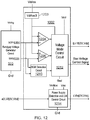
Figure 12 illustrates an embodiment of the supply voltage detector that can be employed in the controller ofFigure 10 . - The use of the same reference symbols in different drawings indicates similar or identical items.
- Disclosed is a control circuit for protecting MOSFETs in I/O buffers or other devices from overvoltage damage, especially during power ramp up, and additional functions. I/O buffers should be tristated when the core supply voltage Vdd and the output supply voltage Vddio are below respective threshold values, which is often the case when Vdd and Vddio are ramping up. If not tristated I/O buffers may send signal "glitches" to external components during voltage ramp up. The control circuit of this disclosure can tristate I/O buffers when Vdd or Vddio are below respective threshold values to prevent them from sending signal glitches.
- To illustrate problems caused by overvoltage,
Figure 1 illustrates anIC 100 in block diagram form, which containscore circuit 102 in data communication with a bank of I/O buffer circuits 104 viadata bus 106.Core circuit 102 is coupled between supply voltage Vdd and ground Gnd=0V.Core circuit 102 may include various devices including a central processing unit (CPU) that communicates directly or indirectly with external components via I/O buffers 104.Figure 2 illustrates relevant components of an example I/O buffer 104, which includes anoutput stage 202 coupled between output supply voltage Vddio and ground Gnd=0V.Output stage 202 includes a stack of MOSFETs 210-216 and aninverter circuit 218. -
Core circuit 102 andoutput stage 202 operate in distinct voltage domains. A binary signal in the core voltage domain has logic voltage levels [0V,Vdd], where 0V is the logic low voltage, and Vdd is the logic high voltage level. A binary signal in the output voltage domain has logic voltage levels [0V,Vddio], where 0V is the logic low voltage, and Vddio is the logic high voltage level. Level shifters can translate the voltage levels of signals. Level shifters are commonly employed in I/O buffers to translate the voltage levels of signals as they move from the core voltage domain to the output voltage domain. Each I/O buffer 104 includes alevel shifter circuit 204 that translates the logic levels of data signal d from [0V,Vdd] to [0V,Vddio]. - At power up, supply voltages Vdd and Vddio are initially at 0V and increase until they reach target levels (e.g., Vdd=0.8V and Vddio=3.3V). I/
O buffers 104 should be tristated until Vdd and Vddio reach respective minimum voltage values. With continuing reference toFigures 1 and2 ,IC 100 includes a power management control (PMC) circuit that controls I/O buffers 104 via a low voltage inhibiter (LVI) signal.PMC circuit 112 asserts LVI (i.e., LVI=Vddio) when supply voltages Vdd or Vddio are below respective minimum thresholds V1 and V2, respectively.MOSFETs O buffers 104 receive the LVI signal and its inversion fromPMC 112 andinverter circuit 218. When LVI is asserted,MOSFETs result output stage 202 is tristated. When Vdd and Vddio are respectively V1 and V2 or higher,PMC 112 de-asserts LVI signal (i.e., LVI=0V), which in turn activatesMOSFETs Output stage 202 can then drive I/O pad 110 based upon input signal d received fromlevel shifter 204. Table 114 shows the state of LVI based on supply voltages Vdd and Vddio. - MOSFETs can be damaged if subjected to voltages that exceed their maximum rating TrMax. For example, if Vgd or Vgs of any of the MOSFETs 210 - 218 exceeds TrMax, that MOSFET can be rendered permanently inoperable. In the example shown within
Figures 1 and2 , TrMax for all of the MOSFETs in I/O buffer 104 andPMC 112 are greater than supply voltages Vdd and Vddio. Accordingly, there is no risk that any of the devices, including MOSFETs 210-218, will be damaged by overvoltage. -
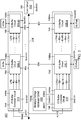
Figure 3 illustrates anIC 300 in block diagram employing MOSFETs that have a lower TrMax when compared to that of the MOSFETs employed withinIC 100 ofFigure 1 . For the purposes of explanationFigure 3 will be described with MOSFETs having a maximum rating of TrMax=1.8V. IC 300 containscore circuit 302 in data communication with a first bank of I/O buffer circuits 304 and a second bank of I/O buffer circuits 306 viadata bus 308.Core circuit 302 is coupled between Vdd=0.8V and Gnd=0V.Core circuit 302 may include various devices including a CPU that that communicate with external components via I/O buffers 304 or I/O buffers 306. - As will be more fully described below each of the I/
O buffers 304 includes an output interface that includes an output stage coupled between output supply voltage Vddio=3.3V and Gnd=0V. The I/O buffers 304 are also referred to herein as the 33I/O buffers 304. Each of the I/O buffers 306 includes an output interface that includes an output stage coupled between output supply Vddiox and Gnd=0V, where Vddiox can vary between 1.8V and 3.3V. For the purposes of explanation, Vddiox=1.8V or Vddiox=3.3V. The I/O buffers 306 are also referred to herein as the 3318I/O buffers 306. - Vdd=0.8V is less than TrMAx=1.8V, and as a result MOSFETs coupled to Vdd will not be damaged by overvoltage. However, output supply voltage Vddio=3.3V exceeds TrMAx=1.8V, and as a result MOSFETs coupled to Vddio can be damaged. The same is true for MOSFETs coupled to Vddiox when it is set to 3.3V. As will be more for described below, protection MOSFETs can be added to avoid overvoltage damage. Noticeably lacking from IC 300 is a PMC circuit like that shown in
Figure 1 . - With continuing reference to
Figure 3 ,Figure 4 illustrates relevant components of an example 33I/O buffer 304, which includes anoutput stage 402 coupled between output supply voltage Vddio and Gnd=0V.Output stage 402 includes a stack of MOSFETs 404-414 andinverter circuit 416. 33I/O buffer 304 receives low voltage inhibit (LVI) control signals LVIp and LVIn from I/Obuffer controller circuit 314.Output stage 402 is tri-stated when P-channel MOSFET 404 and N-channel MOSFET 414 are deactivated when LVIp and LVIn are asserted (i.e, LVIp=Vddio and LVIn=Vddio/2), respectively. Other circuit structures for tri-stating the output stages are contemplated. As noted inFigure 4 , LVIp and LVIn have distinct logic levels [Vddio/2=1.65V, Vddio=3.3V] and [0V, Vddio/2=1.65V], respectively, to ensure that Vgs and Vgd voltages ofMOSFETs V. MOSFETs MOSFETs result MOSFETs O buffer 306. -
Core circuit 302 andoutput stage 402 operate in separate voltage domains. To accommodate the difference, and to prevent overvoltage damage to MOSFETs 406 and 412, each 33I/O buffer 304 includes a splitlevel shifter circuit 420 that translates input data signal d with logic levels [0V, Vdd] into output data signal dn and dp with logic levels [0V, Bn≈1.65V] and [Bp≈1.65V, Vddio=3.3V], respectively, during normal operation of 33I/O buffer 304. During sleep mode, splitlevel shifter circuit 420 translates input data signals d into output data signals dn and dp with logic levels [0V, Bn=1.5V] and [Bp=1.8V, Vddio=3.3V], respectively. The 3318I/O Buffer - With continuing reference to
Figure 3 ,Figure 5 illustrates relevant components of an example 3318I/O buffer 306, which includes anoutput stage 502 coupled between Gnd=0V and output supply voltage Vddiox, which can be either 3.3V or 1.8V. Output stage 502 includes a stack of MOSFETs 504-514. 3318I/O buffer 306 receives low-voltage inhibitor LVIxp and LVIxn control signals from I/Obuffer controller circuit 316.Output stage 502 can be tri-stated when P-channel MOSFET 504 and N-channel MOSFET 514 are deactivated by LVIxp and the inversion of LVIn, respectively. LVIxp and LVIxn for the 3318I/O buffers 306 have different logic levels [Vddiox/2=1.65V, Vddiox=3.3V] and [0V, Vddiox/2=1.65V], respectively, to ensure that Vgs and Vgd voltages ofMOSFETs O buffer 306 also includes aprogrammable bias generator 522 for generating Bxn and Bxp based on an input signal En18, which is asserted by 3318I/O buffer controller 316 when Vddiox=1.8V. With En18 asserted, programmablebias voltage generator 522 outputs Bxp=Vddiox=1.8V and Bxn=0V. When En18 is not asserted, which will be the case when Vddiox=3.3V, programmablebias voltage generator 522 outputs Bxp=Bxn=Vddiox/2=1.65V. MOSFETs MOSFETs -
Core circuit 302 andoutput stage 502 operate in separate voltage domains Vdd=0.8V and Vddiox=1.8V or Vddiox=3.3V. To accommodate the difference, each 3318I/O buffer 306 includes a splitlevel shifter circuit 520 that translates input data signal dx with logic levels [0V,Vdd] into output data signals dxn and dxp with logic levels [0V,Bxp] and [Bxn,Vddiox], respectively. As noted above Bxn=Bxp=Vddiox/2=1.65V when Vddiox=3.3V, and splitlevel shifter 520 translates the input data signals to output data signals dxn and dxp with logic levels [0V,1.65V] and [1.65V,3.3V] to prevent overvoltage damage to MOSFETs 506 and 512. When En18 is asserted (i.e., Vddiox=1.8V), programmablebias voltage generator 522 sets Bxn=0V and Bxp=Vddiox=1.8V, and splitlevel shifter 520 translates the input data signals to output data signals dn and dp with logic levels [0V, 1.8V]. - With continuing reference to
Figures 3-5 ,IC 300 includes I/O buffer controller 314 and I/O buffer controller 316 for controlling the 33I/O buffers 304 and 3318I/O buffers 306, respectively. These I/O buffer controllers perform various control functions. For example I/O buffer controllers IC 300 lacks the powermanagement control circuit 114 ofFigure 1 . I/O buffer controller 314 can also control the biasing voltages Bn and Bp for 33I/O buffers 304 based upon a sleep signal Sleep that is received fromcore circuit 302. I/O buffer controller 316 can generate the En18 signal that controls the programmablebias voltage generator 522 in each 3318I/O buffer 306 based upon supply voltage Vddiox. Additional functions are contemplated. I/O buffer controller 314 will also be referred to as the 33I/O buffer controller 314, and I/O buffer controller 316 will also be referred to as the 33181/0buffer controller 316. -
Figure 6 is a block diagram illustrating an example 33I/O buffer controller 314. With continuing reference toFigures 3 and4 , the 33I/O buffer controller 314 inFigure 6 includes a powersupply detection circuit 602 that receives an eLVI1 signal fromcore circuit 302. Thecore circuit 302 can assert eLVI1 and/or eLVI2 in response toIC 300 receiving a restart or reset signal. The 33I/O buffers 304 and 3318 I/O buffers 306 should tristate when eLVI1 and eLVI2 are asserted.Core circuit 302 can de-assert eLVI1 in response to receiving a signal from a circuit external to IC 302 (e.g., an external PMC circuit similar to that shown inFigure 1 ), which should indicate that Vdd and Vddio are greater than minimum thresholds V1 and V2, respectively, andcore circuit 302 should de-assert eLVI2 in response to receiving the same signal or a different signal from the external circuit that indicates that Vdd and Vddiox exceed minimum thresholds. Unfortunately the signal(s) received bycore circuit 302 may be in error, and Vdd and Vddio may be below V1 and V2, respectively, or Vdd and Vddiox may not exceed minimum thresholds whencore circuit 302 de-asserts eLVI1 and/or eLVI2, which could lead to 33I/O buffers 304 or 3318 I/O buffers 306 sending glitch errors to components external toIC 300. Accordingly, 33I/O buffers 304 and 3318 I/O buffers 306 should not be controlled solely based on the state of eLVI1 and eLVI2. -
Power supply detection 602 generates LVI based upon eLVI1 and a comparison of core voltage supply Vdd and output voltage supply Vddio to reference voltages V1 and V2, respectively.Figure 6 shows a table 604 that defines logic circuits employed withinpower supply detection 602 for generating the LVI signal. Essentiallypower supply detection 602 will not assert the LVI signal until both Vdd and Vddio exceed V1 and V2, respectively, and eLVI1 is asserted (eLVI=Vdd). - The 33I/
O buffer controller 314 includes a split domainlevel shifter circuit 606 that receives the LVI signal frompower supply detection 602 with voltage logic levels [0V,Vdd]. Splitdomain level shifter 606 translates the LVI signal it receives into LVIn and LVIp, which have different logic levels.Level shifter 606 transmits LVIn and LVIp to each of the 33I/O buffers 304, where they are used to controlMOSFETs -
Figure 6 also shows that 33I/O buffer controller 314 includes a programmable biasvoltage generator circuit 610. This device generates biasing voltages Bn and Bp for the 33I/O buffers 304 based on the Sleep signal received fromcore circuit 302 or the LVI signal from power supply detection andLVI control 602. When Sleep is asserted, Bn and Bp are adjusted to put the 33I/O buffers 304 into a low-power mode.Figure 7 illustrates one embodiment of the programmablebias voltage generator 610 in block diagram form, which includes an independent biasvoltage generator circuit 702 coupled between Vddio and Gnd=0V. This device generates a separate set of biasing voltages Bns=Vddio/2 and Bps≈Vddio/2 forlevel shifter circuit 704 and split domainlevel shifter circuit 706.Level shifter 704 translates the Sleep signal fromcore circuit 302 or the LVI signal from power supply detection andLVI control 602 with logic levels [0V,Vdd] into bias voltage control (BVC) signal with logic levels [0V,Bns≈Vddio/2] before it is provided to split domainlevel shifter circuit 706.Split level shifter 606 translates the BVC signal into BVCp with logic levels [Bps≈Vddio,Vddio/2] and BVCn with logic levels [0V, Bns≈Vddio/2]. BVCp and BVCn control I/O biasvoltage generator circuit 710, which in turn generates biasing voltages Bp and Bn for the 33I/O buffers 304. More specifically, if the Sleep signal or the LVI signal is asserted (i.e., Sleep=Vdd or LVI=Vdd), BVCp and BVCn will be asserted high and low (i.e, BVCp=Vddio and BVCn= 0V), respectively. In response, I/Obias voltage generator 710 will bias I/O buffer devices 304 with Bp=Sp=0.55·Vddio≈1.8V and Bn=Sn=0.45·Vddio≈1.5V. With Bn and Bp set at these voltages, the 33I/O buffers 304 will consume less power when compared to the power consumed during normal operation. When Sleep and LVI are not asserted, splitlevel shifter 706 outputs BVCp= Bps=Vddio/2 and BVCn= Bns=Vddio/2. In response, I/Obias voltage generator 710 will bias I/O buffer devices 304 with Bn≈Vddio/2 and Bp≈Vddio/2, which might be slightly different magnitude. -
Figure 8 illustrates an example of a split level shifter that can be employed in theIC 300. More particularly,Figure 8 illustrates an examplesplit level shifter 706 that can be employed within programmablebias voltage generator 610 ofFigure 7 . With continuing reference toFigure 7 , thesplit level shifter 706 shown inFigure 8 includes 2 stacks ofMOSFETs first stack 802 includes a pair of P-channel MOSFETs channel MOSFETs second stack 804 includes a pair of P-channel MOSFETs channel MOSFETs Inverter circuit 830 and the gate of N-channel MOSFET 812 receive BVC[0V,Bns] fromlevel shifter 704. The output ofinverter 830 is received at the gate of N-channel MOSFET 822. Bias voltage Bps is received at the gates of P-channel MOSFETs channel MOSFETs channel MOSFETs channel MOSFETs MOSFETs MOSFETs - As noted in
Figure 7 , control signals BVCp and BVCn are provided to I/Obias voltage generator 710. These control signals determine the magnitudes of bias voltages Bp and Bn that are subsequently provided to the 33 I/O buffers 304.Figure 9 illustrates an example I/Obias voltage generator 710 that can be employed within the programmablebias voltage generator 610 shown withinFigure 7 . With continuing reference toFigures 7 and9 bias voltage generator 710 includesseparate voltage dividers Voltage divider 902 includes stack of MOSFETs 912-926 coupled between Vddio and Gnd=0V as shown. Similarlyvoltage divider 904 includes stack of MOSFETs 932-946 coupled between Vddio and Gnd=0V as shown. Lastly,voltage divider 906 includes a high impedance stack of resistors R1-R6 arranged in series as shown between Vddio and Gnd=0V.Bias generation circuit 710 generates bias voltages Bp and Bn atnodes Figure 9 output node 950 is coupled to the drains of P-channel MOSFETs 918 and N-channel MOSFET 920, whileoutput node 952 is coupled to the drains ofMOSFETs -
Voltage dividers channel MOSFETs split level shifter 706, while the gates of N-channel MOSFETs split level shifter 706 generates BVCp=Vddio and BVCn= 0V, which deactivatesvoltage dividers MOSFETs voltage divider 906 will generate Bn=Sn=1.5V and Bp=Sp=1.8V atnodes level shifter 706 generates BVCp=Bps=Vddio/2=1.65V and BVCn=Bps=Vddio/2=1.65V, which in turn activatesMOSFETs voltage dividers V nodes -
IC 300 ofFigure 3 includes a 3318 I/O buffer controller 316 for controlling 3318 I/O buffers 306 via the LVIxn, LVIxp, Bni, Bpi and En18. As shown the 3318 I/O buffer controller 316 receives stable voltage references BGR1 and BGR2 from a bandgap voltagereference generator circuit 320, which is a device that produces fixed (constant) voltages regardless of power supply variations, temperature changes and circuit loading. BGR1 and BGR2 can be used to determine whether the 3318 I/O buffers 306 are operating with Vddiox=1.8V or Vddiox=3.3V. - With continuing reference to
Figures 3 ,5 ,Figure 10 illustrates an example 3318I/O buffer controller 316. 3318I/O buffer controller 316 includes asupply voltage detector 1002 and a programmable splitdomain level shifter 1004.Supply voltage detector 1002 receives BGR1 and BGR2 frombandgap voltage generator 320, and eLVI2 fromcore circuit 302. Supplyvoltage detector circuit 1002 generates LVIx based upon a comparison of Vdd and Vddiox to threshold voltages V1 and V2, respectively, and based upon the state of eLVI2. Table 1006 defines operational aspects of logic circuits employed withinsupply voltage detector 1002 for generating the LVIs signal. Essentially supply voltage detector asserts the LVIx signal unless both Vdd and Vddiox exceed V1 and V2, respectively, and eLVI2 is asserted (eLVI2=Vdd). -
Supply voltage detector 1002 generates En18, the signal that controls programmable splitdomain level shifter 1004 and the programmablebias voltage generator 522 ofFigure 5 . Programmable splitdomain level shifter 1004 receives both LVIx and En18 fromvoltage supply detector 1002. If En18 asserted, which means Vddiox is presumed equal to 1.8V, programmable splitdomain level shifter 1004 generates LVIxp and LVIxn with voltage levels [0V,Vddiox]. If, however, En18 is not asserted, which means Vddiox is presumed equal to 3.3V, programmable splitdomain level shifter 1004 generates LVIxn and LVIxp with voltage levels [0V,Vddiox/2] and [Vddiox/2,Vddio].Supply voltage detector 1002 compares Vddiox with BGR1 and/or BGR2. In one embodiment,supply voltage detector 1002 determines whether BGR1<Vddiox/3<BGR2. If it is, bias voltage generator circuit 1008, in response to a signal fromsupply voltage detector 1002, changes bias voltages Bpi and Bni to 0.75*Vddiox, and the bias voltages remain at that level until BGR2 < Vddiox/3 at which point bias voltage generator circuit 1008 generates Bpi and Bni at ∼Vddiox/2. -
Figure 11 illustrates relevant aspects of the process employed by thesupply voltage detector 1002 when generating En18. More particularly, the process inFigure 11 begins whenIC 300 reset is detected, and Vddiox starts ramping up from 0V.Supply voltage detector 1002 may detect IC reset when eLVI2 is asserted bycore circuit 302.Supply voltage detector 1002 initially asserts En18=Vdd as shown instep 1104. Programmable biasvoltage generator circuit 522 in each of the 3318I/O buffers 306 drives the gates ofprotection MOSFETs MOSFETs Supply voltage detector 1002 then determines instep 1106 whether BGR1 and BGR2 are greater than 0V. If BGR1=BGR2=0V,supply voltage detector 1002 sets En18=0V as shown instep 1110. Programmable biasvoltage generator circuits 522 in each of the 3318I/O buffers 306 drives the gates ofprotection MOSFETs MOSFETs supply voltage detector 1002 determines that BGR1 and BGR2 are greater than 0V, then supplyvoltage detector 1002 compares Vddiox with BGR1. Ifsupply voltage detector 1002 determines that Vddiox/3 <BGR1 instep 1114, then supplyvoltage detector 1002 reasserts En18 (i.e., En18=Vdd) instep 1116.Supply voltage detector 1002 continues to compare Vddiox with BGR1 afterstep 1116 and while En18 is asserted. However, ifsupply voltage detector 1002 determines that Vddiox/3 increases beyond BGR1, then instep 1122supply voltage detector 1002 resets En18 back to 0V, and the gates ofMOSFETs - With continuing reference to
Figures 10 and11 ,Figure 12 illustrates an embodiment of thesupply voltage detector 1002, which includes a pair ofcomparators BGR detection circuit 1210 and a voltagemode control circuit 1212.Comparators circuit 1203 to BGR1 and BGR2, respectively.Comparators mode control circuit 1212 uses the output ofcomparator 1204 to determine the magnitude of Vddiox insteps Figure 11 . Voltagemode control circuit 1212 usescomparators BGR detection circuit 1210 also receives BGR1 and BGR2 from thebandgap generator 320, and determines whether BGR1 and/or BGR2 are greater than 0V. Voltagemode control circuit 1212 uses the output ofBGR detection circuit 1210 to determine whether one or more of the BGRs are equal to 0V insteps Figure 11 . Lastly, like 33I/O buffer controller 314,supply voltage detector 1002 ofFigure 12 includes a powersupply detection circuit 1214 that generates LVIx based upon Vdd, Vddiox, and eLVI2. More particularly, asserts LVIx when supply voltage Vdd or supply voltage Vddiox are below threshold voltages V1 and V2, respectively, or when eLVI2 is asserted. Programmable splitdomain level shifter 1004 asserts LVIxn and LVIxp when powersupply detection circuit 1214 asserts LVIx, which in turn causes 3318 I/O buffers 306 to enter the tri-state mode. - In a first aspect there is provided an integrated circuit (IC) comprising: input/output (I/O) buffers coupled to an output supply voltage terminal that is configured to receive an output supply voltage Vddio, where each of the I/O buffers comprises: a bias voltage generator that is configured to generate a first bias voltage with a magnitude that depends on a control signal; an output stage that receives the first bias voltage, wherein the output stage is configured to drive an I/O pad based upon a data signal received at the I/O buffer, and; an I/O buffer controller coupled to the I/O buffers and configured to generate the control signal based upon a magnitude of the output supply voltage Vddio.
- In one or more embodiments the output stage of each I/O buffer may comprise: first and second P-channel MOSFETs coupled in series; first and second N-channel MOSFETs coupled in series;
wherein the series coupled P-channel MOSFETs are coupled in series with the series coupled N-channel MOSFETs between the output supply voltage Vddio terminal and a ground terminal;
wherein drains of the second P-channel MOSFET and the first N-channel MOSFET are connected together and to the I/O pad; wherein a gate of the second P-channel MOSFET is coupled to receive the first bias voltage. - In one or more embodiments the bias voltage generator of each I/O buffer is configured to generate a second bias voltage that is received by the output stage of the I/O buffer, wherein the second bias voltage has a magnitude that depends upon the control signal.
- In one or more embodiments a gate of the second P-channel MOSFET in each of the I/O buffers is coupled to receive the second bias voltage generated by the bias voltage generator of the I/O buffer.
- In one or more embodiments the bias generator generates the first and second bias voltages with magnitudes that are substantially equal to each other when the control signal is at a first logic voltage level.
- In one or more embodiments the bias generator generates the first and second bias with magnitudes that are substantially equal to each other when the control signal is at a second logic voltage level.
- In one or more embodiments, the IC further comprises: a bandgap voltage generator configured to generate a first bandgap reference voltage; wherein the I/O buffer controller is configured to compare the output supply voltage Vddio to be first bandgap reference voltage;
- wherein the I/O buffer controller is configured to generate the control signal based upon the comparison of the output supply voltage Vddio to the first bandgap reference voltage.
- In one or more embodiments, the bandgap voltage generator configured to generate a second bandgap reference voltage; the I/O buffer controller is configured to compare the output supply voltage Vddio to be second bandgap reference voltage; the I/O buffer controller is configured to generate the control signal based upon the comparison of the output supply voltage Vddio to the first bandgap reference voltage and the comparison of the output supply voltage Vddio to the second bandgap reference voltage.
- In second aspect there is provided an integrated circuit (IC) comprising: a core circuit coupled to a core supply voltage terminal that is configured to receive a core supply voltage Vdd; input/output (I/O) buffers coupled to an output supply voltage terminal that is configured to receive an output supply voltage Vddio, wherein each of the I/O buffers comprises an output stage to drive an I/O pad based upon data signal received at the I/O buffer; an I/O buffer controller coupled to the I/O buffers and configured to generate first and second control signals based upon magnitudes of the core supply voltage Vdd and the output supply voltage Vddio;
- wherein the first and second control signals control the output stages.
- In one or more embodiments, the input output stage in each of the I/O buffers is inhibited from driving its I/O pad when the I/O buffer controller generates the first and second control signals with respective logic high voltages; wherein the input output stage in each of the I/O buffers is enabled to drive its I/O pad when the I/O buffer controller generates the first and second control signals with respective logic low voltages.
- In one or more embodiments, the I/O buffer controller generates the first and second control signals with respective logic low voltages when magnitudes of core supply voltage Vdd and output supply voltage Vddio are below threshold voltages V1 and V2, respectively.
- In one or more embodiments, the core circuit is configured to generate an inhibit signal when the core circuit receives a signal from a device external to the IC; the I/O buffer controller generates the first and second control signals with respective logic high voltages when magnitudes of core supply voltage Vdd and output supply voltage Vddio are below threshold voltages V1 and V2, respectively, and when the inhibit signal is asserted.
- In one or more embodiments, each of the I/O buffers comprises a bias voltage generator that is configured to generate a first bias voltage with a magnitude that depends on another control signal; wherein the output stage of each of the I/O buffers receives the first bias voltage from its bias voltage generator; wherein the I/O buffer controller is configured to generate the other control signal based upon a magnitude of the output supply voltage Vddio.
- In third aspect there is provided an integrated circuit comprising: a core circuit that is configured to generate a sleep signal; input/output (I/O) buffers each comprising an output stage configured to drive an I/O pad based upon a data signal received at the I/O buffer, wherein the output stage of each I/O buffer receives a first bias voltage; an I/O buffer controller coupled to the I/O buffers and configured to generate the first bias voltage, wherein a magnitude of the first bias voltage depends upon the sleep signal.
- In one or more embodiments, the output stage of each I/O buffer comprises: first and second P-channel MOSFETs coupled in series; first and second N-channel MOSFETs coupled in series; wherein the series coupled P-channel MOSFETs are coupled in series with the series coupled N-channel MOSFETs between an output supply voltage Vddio terminal and a ground terminal; wherein drains of the second P-channel MOSFET and the first N-channel MOSFET are connected together and to the I/O pad; wherein a gate of the second P-channel MOSFET is coupled to receive the first bias voltage.
- In one or more embodiments, the I/O buffer controller generates a second bias voltage that is received at a gate of each of the first N-channel MOSFETs, wherein the second bias voltage has a magnitude that depends upon the sleep signal.
- In one or more embodiments, the I/O buffer controller is configured to generate the first and second bias voltages with magnitudes that are substantially equal to each other when the sleep signal is asserted; wherein the I/O buffer controller is configured to generate the first and second bias voltages with magnitudes that are substantially different when the sleep signal is not asserted.
- In one or more embodiments, the I/O offer controller comprises first and second bias voltage generators for generating the first and second bias voltages, respectively, when the sleep signal is not asserted; wherein the I/O buffer comprises a third bias voltage generator for generating the first and second bias voltages when the sleep signal is asserted.
- In one or more embodiments, each of the I/O buffers comprises a level shifter that is configured to receive the first and second bias voltages.
- Although the present invention has been described in connection with several embodiments, the invention is not intended to be limited to the specific forms set forth herein. On the contrary, it is intended to cover such alternatives, modifications, and equivalents as can be reasonably included within the scope of the invention as defined by the appended claims.
- Disclosed is a control circuit for protecting MOSFETs in I/O buffers or other devices from overvoltage damage, especially during power ramp up. The control circuit can perform additional functions. In one embodiment an integrated circuit (IC) includes input/output (I/O) buffers coupled to an output supply voltage terminal that is configured to receive an output supply voltage Vddio. Each of the I/O buffers has a bias voltage generator that is configured to generate a first bias voltage with a magnitude that depends on a control signal; an output stage that receives the first bias voltage, wherein the output stage is configured to drive an I/O pad based upon a data signal received at the I/O buffer. The IC also includes an I/O buffer controller coupled to the I/O buffers and configured to generate the control signal based upon a magnitude of the output supply voltage Vddio.
Claims (13)
- An integrated circuit (IC) comprising:input/output (I/O) buffers coupled to an output supply voltage terminal that is configured to receive an output supply voltage Vddio, where each of the I/O buffers comprises: a bias voltage generator that is configured to generate a first bias voltage with a magnitude that depends on a control signal; an output stage that receives the first bias voltage, wherein the output stage is configured to drive an I/O pad based upon a data signal received at the I/O buffer, and;an I/O buffer controller coupled to the I/O buffers and configured to generate a control signal based upon a magnitude of the output supply voltage Vddio.
- The IC of claim 1 wherein the output stage of each I/O buffer comprises:first and second P-channel MOSFETs coupled in series;first and second N-channel MOSFETs coupled in series;wherein the series coupled P-channel MOSFETs are coupled in series with the series coupled N-channel MOSFETs between the output supply voltage Vddio terminal and a ground terminal;wherein drains of the second P-channel MOSFET and the first N-channel MOSFET are connected together and to the I/O pad;wherein a gate of the second P-channel MOSFET is coupled to receive the first bias voltage.
- The IC of claim 1 or 2 wherein the bias voltage generator of each I/O buffer is configured to generate a second bias voltage that is received by the output stage of the I/O buffer, wherein the second bias voltage has a magnitude that depends upon the control signal.
- The IC of claim 3 when dependent on claim 2 wherein a gate of the second P-channel MOSFET in each of the I/O buffers is coupled to receive the second bias voltage generated by the bias voltage generator of the I/O buffer.
- The IC of claim 3 or 4 wherein the bias generator generates the first and second bias voltages with magnitudes that are substantially equal to each other when the control signal is at a first logic voltage level.
- The IC of any of claims 3 to 5 wherein the bias generator generates the first and second bias with magnitudes that are substantially equal to each other when the control signal is at a second logic voltage level.
- The IC of any preceding claim further comprising:a bandgap voltage generator configured to generate a first bandgap reference voltage;wherein the I/O buffer controller is configured to compare the output supply voltage Vddio to be first bandgap reference voltage;wherein the I/O buffer controller is configured to generate the control signal based upon the comparison of the output supply voltage Vddio to the first bandgap reference voltage.
- The IC of claim 7:wherein the bandgap voltage generator configured to generate a second bandgap reference voltage;wherein the I/O buffer controller is configured to compare the output supply voltage Vddio to be second bandgap reference voltage;wherein the I/O buffer controller is configured to generate the control signal based upon the comparison of the output supply voltage Vddio to the first bandgap reference voltage and the comparison of the output supply voltage Vddio to the second bandgap reference voltage.
- An integrated circuit (IC) according to any preceding claim and further comprising:a core circuit coupled to a core supply voltage terminal that is configured to receive a core supply voltage Vdd;I/O buffer controller is further configured to generate first and second control signals based upon magnitudes of the core supply voltage Vdd and the output supply voltage Vddio;wherein the first and second control signals control the output stages.
- The IC of claim 9:wherein the input output stage in each of the I/O buffers is inhibited from driving its I/O pad when the I/O buffer controller generates the first and second control signals with respective logic high voltages;wherein the input output stage in each of the I/O buffers is enabled to drive its I/O pad when the I/O buffer controller generates the first and second control signals with respective logic low voltages.
- The IC of claim 9 or 10 wherein the I/O buffer controller generates the first and second control signals with respective logic low voltages when magnitudes of core supply voltage Vdd and output supply voltage Vddio are below threshold voltages V1 and V2, respectively.
- The IC of claim 11:wherein the core circuit is configured to generate an inhibit signal when the core circuit receives a signal from a device external to the IC;wherein the I/O buffer controller generates the first and second control signals with respective logic high voltages when magnitudes of core supply voltage Vdd and output supply voltage Vddio are below threshold voltages V1 and V2, respectively, and when the inhibit signal is asserted.
- The IC of any of claims 9 to 12:wherein each of the I/O buffers comprises a bias voltage generator that is configured to generate a first bias voltage with a magnitude that depends on another control signal;wherein the output stage of each of the I/O buffers receives the first bias voltage from its bias voltage generator;wherein the I/O buffer controller is configured to generate the other control signal based upon a magnitude of the output supply voltage Vddio.
Applications Claiming Priority (1)
| Application Number | Priority Date | Filing Date | Title |
|---|---|---|---|
| US16/745,605 US11223358B2 (en) | 2020-01-17 | 2020-01-17 | IO analog rail control circuit for power ramps |
Publications (2)
| Publication Number | Publication Date |
|---|---|
| EP3852271A1 true EP3852271A1 (en) | 2021-07-21 |
| EP3852271B1 EP3852271B1 (en) | 2024-03-27 |
Family
ID=73856928
Family Applications (1)
| Application Number | Title | Priority Date | Filing Date |
|---|---|---|---|
| EP20216729.2A Active EP3852271B1 (en) | 2020-01-17 | 2020-12-22 | Io analog rail control circuit for power ramps |
Country Status (2)
| Country | Link |
|---|---|
| US (1) | US11223358B2 (en) |
| EP (1) | EP3852271B1 (en) |
Families Citing this family (4)
| Publication number | Priority date | Publication date | Assignee | Title |
|---|---|---|---|---|
| US11422581B2 (en) * | 2020-08-21 | 2022-08-23 | Arm Limited | Dynamic biasing techniques |
| US12153458B2 (en) * | 2022-12-16 | 2024-11-26 | Xilinx, Inc. | Method for implementing an I/O buffer |
| US12132473B2 (en) | 2023-03-13 | 2024-10-29 | Nxp Usa, Inc. | Switch with cascode arrangement |
| US12126338B1 (en) * | 2023-04-04 | 2024-10-22 | Nxp Usa, Inc. | Switch with cascode arrangement |
Citations (3)
| Publication number | Priority date | Publication date | Assignee | Title |
|---|---|---|---|---|
| US5917358A (en) * | 1997-12-09 | 1999-06-29 | Motorola, Inc. | Method and output buffer with programmable bias to accommodate multiple supply voltages |
| US9893730B1 (en) * | 2017-03-31 | 2018-02-13 | Advanced Micro Devices, Inc. | Three rail level shifter |
| US20190149149A1 (en) * | 2017-09-29 | 2019-05-16 | Taiwan Semiconductor Manufacturing Company Limited | Multi-Voltage Input Output Device |
Family Cites Families (6)
| Publication number | Priority date | Publication date | Assignee | Title |
|---|---|---|---|---|
| US5896045A (en) * | 1997-05-05 | 1999-04-20 | Siegel; Joshua | Static pulsed cross-coupled level shifter and method therefor |
| US6342802B1 (en) | 1999-10-28 | 2002-01-29 | Seagate Technology Llc | Multi-voltage power-up stable input/output buffer circuit in a disc drive |
| US6842058B2 (en) * | 2002-11-12 | 2005-01-11 | Lsi Logic Corporation | Method and apparatus for slew control of an output signal |
| US7193441B2 (en) * | 2004-11-18 | 2007-03-20 | Taiwan Semiconductor Manufacturing Co., Ltd. | Single gate oxide I/O buffer with improved under-drive feature |
| KR102055841B1 (en) * | 2013-03-05 | 2019-12-13 | 삼성전자주식회사 | Output buffer circuit and source driving circuit including the same |
| US9383794B2 (en) | 2014-06-11 | 2016-07-05 | Freescale Semiconductor, Inc. | Integrated circuit with multi-voltage input/output (I/O) cells |
-
2020
- 2020-01-17 US US16/745,605 patent/US11223358B2/en active Active
- 2020-12-22 EP EP20216729.2A patent/EP3852271B1/en active Active
Patent Citations (3)
| Publication number | Priority date | Publication date | Assignee | Title |
|---|---|---|---|---|
| US5917358A (en) * | 1997-12-09 | 1999-06-29 | Motorola, Inc. | Method and output buffer with programmable bias to accommodate multiple supply voltages |
| US9893730B1 (en) * | 2017-03-31 | 2018-02-13 | Advanced Micro Devices, Inc. | Three rail level shifter |
| US20190149149A1 (en) * | 2017-09-29 | 2019-05-16 | Taiwan Semiconductor Manufacturing Company Limited | Multi-Voltage Input Output Device |
Also Published As
| Publication number | Publication date |
|---|---|
| US11223358B2 (en) | 2022-01-11 |
| US20210226630A1 (en) | 2021-07-22 |
| EP3852271B1 (en) | 2024-03-27 |
Similar Documents
| Publication | Publication Date | Title |
|---|---|---|
| EP3852271B1 (en) | Io analog rail control circuit for power ramps | |
| US8073643B2 (en) | Semiconductor device | |
| US7952402B2 (en) | Power-up control for very low-power systems | |
| US6879191B2 (en) | Voltage mismatch tolerant input/output buffer | |
| US8395870B2 (en) | Input/output circuit | |
| JP5690341B2 (en) | Integrated circuit adapted to be selectively AC or DC coupled | |
| US9627962B2 (en) | Fast blocking switch | |
| US7639041B1 (en) | Hotsocket-compatible body bias circuitry with power-up current reduction capabilities | |
| US8054125B2 (en) | Charge pump with low power, high voltage protection circuitry | |
| EP3251150B1 (en) | Self-sensing reverse current protection switch | |
| JP2008532108A (en) | Voltage regulator with bypass mode | |
| US6359459B1 (en) | Integrated circuits including voltage-controllable power supply systems that can be used for low supply voltage margin testing and related methods | |
| US6707722B2 (en) | Method and apparatus for regulating predriver for output buffer | |
| US7619444B1 (en) | Circuit technique to prevent device overstress | |
| KR20220109088A (en) | Electrostatic discharge circuit and electrostatic discharge control system | |
| US6097179A (en) | Temperature compensating compact voltage regulator for integrated circuit device | |
| CN1983756B (en) | System and method to avoid device stressing | |
| US20240275282A1 (en) | Circuit and method for start-up of reference circuits in devices with a plurality of supply voltages | |
| US7123460B2 (en) | Methods and systems for reducing power-on failure of integrated circuits | |
| US7123053B1 (en) | Circuitry for providing overvoltage backdrive protection | |
| JPS5994925A (en) | Integrated power on reset circuit for electric controller | |
| KR100650816B1 (en) | Internal circuit protection device | |
| US6940334B2 (en) | Methods and systems for generating interim voltage supplies | |
| US8542041B2 (en) | Semiconductor device and system | |
| CN100413216C (en) | Circuit arrangement for monitoring supply voltage |
Legal Events
| Date | Code | Title | Description |
|---|---|---|---|
| PUAI | Public reference made under article 153(3) epc to a published international application that has entered the european phase |
Free format text: ORIGINAL CODE: 0009012 |
|
| STAA | Information on the status of an ep patent application or granted ep patent |
Free format text: STATUS: THE APPLICATION HAS BEEN PUBLISHED |
|
| AK | Designated contracting states |
Kind code of ref document: A1 Designated state(s): AL AT BE BG CH CY CZ DE DK EE ES FI FR GB GR HR HU IE IS IT LI LT LU LV MC MK MT NL NO PL PT RO RS SE SI SK SM TR |
|
| STAA | Information on the status of an ep patent application or granted ep patent |
Free format text: STATUS: REQUEST FOR EXAMINATION WAS MADE |
|
| 17P | Request for examination filed |
Effective date: 20220121 |
|
| RBV | Designated contracting states (corrected) |
Designated state(s): AL AT BE BG CH CY CZ DE DK EE ES FI FR GB GR HR HU IE IS IT LI LT LU LV MC MK MT NL NO PL PT RO RS SE SI SK SM TR |
|
| GRAP | Despatch of communication of intention to grant a patent |
Free format text: ORIGINAL CODE: EPIDOSNIGR1 |
|
| STAA | Information on the status of an ep patent application or granted ep patent |
Free format text: STATUS: GRANT OF PATENT IS INTENDED |
|
| INTG | Intention to grant announced |
Effective date: 20231215 |
|
| GRAS | Grant fee paid |
Free format text: ORIGINAL CODE: EPIDOSNIGR3 |
|
| GRAA | (expected) grant |
Free format text: ORIGINAL CODE: 0009210 |
|
| STAA | Information on the status of an ep patent application or granted ep patent |
Free format text: STATUS: THE PATENT HAS BEEN GRANTED |
|
| AK | Designated contracting states |
Kind code of ref document: B1 Designated state(s): AL AT BE BG CH CY CZ DE DK EE ES FI FR GB GR HR HU IE IS IT LI LT LU LV MC MK MT NL NO PL PT RO RS SE SI SK SM TR |
|
| REG | Reference to a national code |
Ref country code: GB Ref legal event code: FG4D |
|
| REG | Reference to a national code |
Ref country code: CH Ref legal event code: EP |
|
| REG | Reference to a national code |
Ref country code: DE Ref legal event code: R096 Ref document number: 602020027864 Country of ref document: DE |
|
| REG | Reference to a national code |
Ref country code: IE Ref legal event code: FG4D |
|
| PG25 | Lapsed in a contracting state [announced via postgrant information from national office to epo] |
Ref country code: LT Free format text: LAPSE BECAUSE OF FAILURE TO SUBMIT A TRANSLATION OF THE DESCRIPTION OR TO PAY THE FEE WITHIN THE PRESCRIBED TIME-LIMIT Effective date: 20240327 |
|
| REG | Reference to a national code |
Ref country code: LT Ref legal event code: MG9D |
|
| PG25 | Lapsed in a contracting state [announced via postgrant information from national office to epo] |
Ref country code: GR Free format text: LAPSE BECAUSE OF FAILURE TO SUBMIT A TRANSLATION OF THE DESCRIPTION OR TO PAY THE FEE WITHIN THE PRESCRIBED TIME-LIMIT Effective date: 20240628 |
|
| PG25 | Lapsed in a contracting state [announced via postgrant information from national office to epo] |
Ref country code: HR Free format text: LAPSE BECAUSE OF FAILURE TO SUBMIT A TRANSLATION OF THE DESCRIPTION OR TO PAY THE FEE WITHIN THE PRESCRIBED TIME-LIMIT Effective date: 20240327 Ref country code: RS Free format text: LAPSE BECAUSE OF FAILURE TO SUBMIT A TRANSLATION OF THE DESCRIPTION OR TO PAY THE FEE WITHIN THE PRESCRIBED TIME-LIMIT Effective date: 20240627 |
|
| PG25 | Lapsed in a contracting state [announced via postgrant information from national office to epo] |
Ref country code: RS Free format text: LAPSE BECAUSE OF FAILURE TO SUBMIT A TRANSLATION OF THE DESCRIPTION OR TO PAY THE FEE WITHIN THE PRESCRIBED TIME-LIMIT Effective date: 20240627 Ref country code: NO Free format text: LAPSE BECAUSE OF FAILURE TO SUBMIT A TRANSLATION OF THE DESCRIPTION OR TO PAY THE FEE WITHIN THE PRESCRIBED TIME-LIMIT Effective date: 20240627 Ref country code: LT Free format text: LAPSE BECAUSE OF FAILURE TO SUBMIT A TRANSLATION OF THE DESCRIPTION OR TO PAY THE FEE WITHIN THE PRESCRIBED TIME-LIMIT Effective date: 20240327 Ref country code: HR Free format text: LAPSE BECAUSE OF FAILURE TO SUBMIT A TRANSLATION OF THE DESCRIPTION OR TO PAY THE FEE WITHIN THE PRESCRIBED TIME-LIMIT Effective date: 20240327 Ref country code: GR Free format text: LAPSE BECAUSE OF FAILURE TO SUBMIT A TRANSLATION OF THE DESCRIPTION OR TO PAY THE FEE WITHIN THE PRESCRIBED TIME-LIMIT Effective date: 20240628 Ref country code: FI Free format text: LAPSE BECAUSE OF FAILURE TO SUBMIT A TRANSLATION OF THE DESCRIPTION OR TO PAY THE FEE WITHIN THE PRESCRIBED TIME-LIMIT Effective date: 20240327 Ref country code: BG Free format text: LAPSE BECAUSE OF FAILURE TO SUBMIT A TRANSLATION OF THE DESCRIPTION OR TO PAY THE FEE WITHIN THE PRESCRIBED TIME-LIMIT Effective date: 20240327 |
|
| REG | Reference to a national code |
Ref country code: NL Ref legal event code: MP Effective date: 20240327 |
|
| PG25 | Lapsed in a contracting state [announced via postgrant information from national office to epo] |
Ref country code: SE Free format text: LAPSE BECAUSE OF FAILURE TO SUBMIT A TRANSLATION OF THE DESCRIPTION OR TO PAY THE FEE WITHIN THE PRESCRIBED TIME-LIMIT Effective date: 20240327 Ref country code: LV Free format text: LAPSE BECAUSE OF FAILURE TO SUBMIT A TRANSLATION OF THE DESCRIPTION OR TO PAY THE FEE WITHIN THE PRESCRIBED TIME-LIMIT Effective date: 20240327 |
|
| PG25 | Lapsed in a contracting state [announced via postgrant information from national office to epo] |
Ref country code: NL Free format text: LAPSE BECAUSE OF FAILURE TO SUBMIT A TRANSLATION OF THE DESCRIPTION OR TO PAY THE FEE WITHIN THE PRESCRIBED TIME-LIMIT Effective date: 20240327 |
|
| REG | Reference to a national code |
Ref country code: AT Ref legal event code: MK05 Ref document number: 1670894 Country of ref document: AT Kind code of ref document: T Effective date: 20240327 |
|
| PG25 | Lapsed in a contracting state [announced via postgrant information from national office to epo] |
Ref country code: NL Free format text: LAPSE BECAUSE OF FAILURE TO SUBMIT A TRANSLATION OF THE DESCRIPTION OR TO PAY THE FEE WITHIN THE PRESCRIBED TIME-LIMIT Effective date: 20240327 |
|
| PG25 | Lapsed in a contracting state [announced via postgrant information from national office to epo] |
Ref country code: IS Free format text: LAPSE BECAUSE OF FAILURE TO SUBMIT A TRANSLATION OF THE DESCRIPTION OR TO PAY THE FEE WITHIN THE PRESCRIBED TIME-LIMIT Effective date: 20240727 |
|
| PG25 | Lapsed in a contracting state [announced via postgrant information from national office to epo] |
Ref country code: SM Free format text: LAPSE BECAUSE OF FAILURE TO SUBMIT A TRANSLATION OF THE DESCRIPTION OR TO PAY THE FEE WITHIN THE PRESCRIBED TIME-LIMIT Effective date: 20240327 Ref country code: PT Free format text: LAPSE BECAUSE OF FAILURE TO SUBMIT A TRANSLATION OF THE DESCRIPTION OR TO PAY THE FEE WITHIN THE PRESCRIBED TIME-LIMIT Effective date: 20240729 |
|
| PG25 | Lapsed in a contracting state [announced via postgrant information from national office to epo] |
Ref country code: ES Free format text: LAPSE BECAUSE OF FAILURE TO SUBMIT A TRANSLATION OF THE DESCRIPTION OR TO PAY THE FEE WITHIN THE PRESCRIBED TIME-LIMIT Effective date: 20240327 |
|
| PG25 | Lapsed in a contracting state [announced via postgrant information from national office to epo] |
Ref country code: CZ Free format text: LAPSE BECAUSE OF FAILURE TO SUBMIT A TRANSLATION OF THE DESCRIPTION OR TO PAY THE FEE WITHIN THE PRESCRIBED TIME-LIMIT Effective date: 20240327 Ref country code: EE Free format text: LAPSE BECAUSE OF FAILURE TO SUBMIT A TRANSLATION OF THE DESCRIPTION OR TO PAY THE FEE WITHIN THE PRESCRIBED TIME-LIMIT Effective date: 20240327 |
|
| PG25 | Lapsed in a contracting state [announced via postgrant information from national office to epo] |
Ref country code: AT Free format text: LAPSE BECAUSE OF FAILURE TO SUBMIT A TRANSLATION OF THE DESCRIPTION OR TO PAY THE FEE WITHIN THE PRESCRIBED TIME-LIMIT Effective date: 20240327 |
|
| PG25 | Lapsed in a contracting state [announced via postgrant information from national office to epo] |
Ref country code: PL Free format text: LAPSE BECAUSE OF FAILURE TO SUBMIT A TRANSLATION OF THE DESCRIPTION OR TO PAY THE FEE WITHIN THE PRESCRIBED TIME-LIMIT Effective date: 20240327 |
|
| PG25 | Lapsed in a contracting state [announced via postgrant information from national office to epo] |
Ref country code: SK Free format text: LAPSE BECAUSE OF FAILURE TO SUBMIT A TRANSLATION OF THE DESCRIPTION OR TO PAY THE FEE WITHIN THE PRESCRIBED TIME-LIMIT Effective date: 20240327 |
|
| PG25 | Lapsed in a contracting state [announced via postgrant information from national office to epo] |
Ref country code: SM Free format text: LAPSE BECAUSE OF FAILURE TO SUBMIT A TRANSLATION OF THE DESCRIPTION OR TO PAY THE FEE WITHIN THE PRESCRIBED TIME-LIMIT Effective date: 20240327 Ref country code: SK Free format text: LAPSE BECAUSE OF FAILURE TO SUBMIT A TRANSLATION OF THE DESCRIPTION OR TO PAY THE FEE WITHIN THE PRESCRIBED TIME-LIMIT Effective date: 20240327 Ref country code: RO Free format text: LAPSE BECAUSE OF FAILURE TO SUBMIT A TRANSLATION OF THE DESCRIPTION OR TO PAY THE FEE WITHIN THE PRESCRIBED TIME-LIMIT Effective date: 20240327 Ref country code: PT Free format text: LAPSE BECAUSE OF FAILURE TO SUBMIT A TRANSLATION OF THE DESCRIPTION OR TO PAY THE FEE WITHIN THE PRESCRIBED TIME-LIMIT Effective date: 20240729 Ref country code: PL Free format text: LAPSE BECAUSE OF FAILURE TO SUBMIT A TRANSLATION OF THE DESCRIPTION OR TO PAY THE FEE WITHIN THE PRESCRIBED TIME-LIMIT Effective date: 20240327 Ref country code: IS Free format text: LAPSE BECAUSE OF FAILURE TO SUBMIT A TRANSLATION OF THE DESCRIPTION OR TO PAY THE FEE WITHIN THE PRESCRIBED TIME-LIMIT Effective date: 20240727 Ref country code: ES Free format text: LAPSE BECAUSE OF FAILURE TO SUBMIT A TRANSLATION OF THE DESCRIPTION OR TO PAY THE FEE WITHIN THE PRESCRIBED TIME-LIMIT Effective date: 20240327 Ref country code: EE Free format text: LAPSE BECAUSE OF FAILURE TO SUBMIT A TRANSLATION OF THE DESCRIPTION OR TO PAY THE FEE WITHIN THE PRESCRIBED TIME-LIMIT Effective date: 20240327 Ref country code: CZ Free format text: LAPSE BECAUSE OF FAILURE TO SUBMIT A TRANSLATION OF THE DESCRIPTION OR TO PAY THE FEE WITHIN THE PRESCRIBED TIME-LIMIT Effective date: 20240327 Ref country code: AT Free format text: LAPSE BECAUSE OF FAILURE TO SUBMIT A TRANSLATION OF THE DESCRIPTION OR TO PAY THE FEE WITHIN THE PRESCRIBED TIME-LIMIT Effective date: 20240327 |
|
| PG25 | Lapsed in a contracting state [announced via postgrant information from national office to epo] |
Ref country code: IT Free format text: LAPSE BECAUSE OF FAILURE TO SUBMIT A TRANSLATION OF THE DESCRIPTION OR TO PAY THE FEE WITHIN THE PRESCRIBED TIME-LIMIT Effective date: 20240327 |
|
| PG25 | Lapsed in a contracting state [announced via postgrant information from national office to epo] |
Ref country code: IT Free format text: LAPSE BECAUSE OF FAILURE TO SUBMIT A TRANSLATION OF THE DESCRIPTION OR TO PAY THE FEE WITHIN THE PRESCRIBED TIME-LIMIT Effective date: 20240327 |
|
| REG | Reference to a national code |
Ref country code: DE Ref legal event code: R097 Ref document number: 602020027864 Country of ref document: DE |
|
| PG25 | Lapsed in a contracting state [announced via postgrant information from national office to epo] |
Ref country code: DK Free format text: LAPSE BECAUSE OF FAILURE TO SUBMIT A TRANSLATION OF THE DESCRIPTION OR TO PAY THE FEE WITHIN THE PRESCRIBED TIME-LIMIT Effective date: 20240327 |
|
| PG25 | Lapsed in a contracting state [announced via postgrant information from national office to epo] |
Ref country code: DK Free format text: LAPSE BECAUSE OF FAILURE TO SUBMIT A TRANSLATION OF THE DESCRIPTION OR TO PAY THE FEE WITHIN THE PRESCRIBED TIME-LIMIT Effective date: 20240327 |
|
| PLBE | No opposition filed within time limit |
Free format text: ORIGINAL CODE: 0009261 |
|
| STAA | Information on the status of an ep patent application or granted ep patent |
Free format text: STATUS: NO OPPOSITION FILED WITHIN TIME LIMIT |
|
| 26N | No opposition filed |
Effective date: 20250103 |
|
| PG25 | Lapsed in a contracting state [announced via postgrant information from national office to epo] |
Ref country code: SI Free format text: LAPSE BECAUSE OF FAILURE TO SUBMIT A TRANSLATION OF THE DESCRIPTION OR TO PAY THE FEE WITHIN THE PRESCRIBED TIME-LIMIT Effective date: 20240327 |
|
| PG25 | Lapsed in a contracting state [announced via postgrant information from national office to epo] |
Ref country code: MC Free format text: LAPSE BECAUSE OF FAILURE TO SUBMIT A TRANSLATION OF THE DESCRIPTION OR TO PAY THE FEE WITHIN THE PRESCRIBED TIME-LIMIT Effective date: 20240327 |
|
| P01 | Opt-out of the competence of the unified patent court (upc) registered |
Free format text: CASE NUMBER: APP_29878/2025 Effective date: 20250623 |
|
| REG | Reference to a national code |
Ref country code: CH Ref legal event code: PL |
|
| PG25 | Lapsed in a contracting state [announced via postgrant information from national office to epo] |
Ref country code: LU Free format text: LAPSE BECAUSE OF NON-PAYMENT OF DUE FEES Effective date: 20241222 |
|
| GBPC | Gb: european patent ceased through non-payment of renewal fee |
Effective date: 20241222 |
|
| REG | Reference to a national code |
Ref country code: BE Ref legal event code: MM Effective date: 20241231 |
|
| PG25 | Lapsed in a contracting state [announced via postgrant information from national office to epo] |
Ref country code: BE Free format text: LAPSE BECAUSE OF NON-PAYMENT OF DUE FEES Effective date: 20241231 Ref country code: GB Free format text: LAPSE BECAUSE OF NON-PAYMENT OF DUE FEES Effective date: 20241222 |
|
| PG25 | Lapsed in a contracting state [announced via postgrant information from national office to epo] |
Ref country code: FR Free format text: LAPSE BECAUSE OF NON-PAYMENT OF DUE FEES Effective date: 20241231 |
|
| PG25 | Lapsed in a contracting state [announced via postgrant information from national office to epo] |
Ref country code: CH Free format text: LAPSE BECAUSE OF NON-PAYMENT OF DUE FEES Effective date: 20241231 |
|
| PG25 | Lapsed in a contracting state [announced via postgrant information from national office to epo] |
Ref country code: IE Free format text: LAPSE BECAUSE OF NON-PAYMENT OF DUE FEES Effective date: 20241222 |
|
| PGFP | Annual fee paid to national office [announced via postgrant information from national office to epo] |
Ref country code: DE Payment date: 20251126 Year of fee payment: 6 |