EP3852151A1 - Infrared sensor and method for producing same - Google Patents
Infrared sensor and method for producing same Download PDFInfo
- Publication number
- EP3852151A1 EP3852151A1 EP19859093.7A EP19859093A EP3852151A1 EP 3852151 A1 EP3852151 A1 EP 3852151A1 EP 19859093 A EP19859093 A EP 19859093A EP 3852151 A1 EP3852151 A1 EP 3852151A1
- Authority
- EP
- European Patent Office
- Prior art keywords
- quantum dot
- infrared sensor
- light absorption
- layer
- absorption layer
- Prior art date
- Legal status (The legal status is an assumption and is not a legal conclusion. Google has not performed a legal analysis and makes no representation as to the accuracy of the status listed.)
- Pending
Links
Images



Classifications
-
- H—ELECTRICITY
- H10—SEMICONDUCTOR DEVICES; ELECTRIC SOLID-STATE DEVICES NOT OTHERWISE PROVIDED FOR
- H10F—INORGANIC SEMICONDUCTOR DEVICES SENSITIVE TO INFRARED RADIATION, LIGHT, ELECTROMAGNETIC RADIATION OF SHORTER WAVELENGTH OR CORPUSCULAR RADIATION
- H10F39/00—Integrated devices, or assemblies of multiple devices, comprising at least one element covered by group H10F30/00, e.g. radiation detectors comprising photodiode arrays
- H10F39/10—Integrated devices
- H10F39/12—Image sensors
- H10F39/191—Photoconductor image sensors
- H10F39/193—Infrared image sensors
-
- G—PHYSICS
- G01—MEASURING; TESTING
- G01J—MEASUREMENT OF INTENSITY, VELOCITY, SPECTRAL CONTENT, POLARISATION, PHASE OR PULSE CHARACTERISTICS OF INFRARED, VISIBLE OR ULTRAVIOLET LIGHT; COLORIMETRY; RADIATION PYROMETRY
- G01J5/00—Radiation pyrometry, e.g. infrared or optical thermometry
- G01J5/02—Constructional details
- G01J5/08—Optical arrangements
- G01J5/0853—Optical arrangements having infrared absorbers other than the usual absorber layers deposited on infrared detectors like bolometers, wherein the heat propagation between the absorber and the detecting element occurs within a solid
-
- G—PHYSICS
- G01—MEASURING; TESTING
- G01J—MEASUREMENT OF INTENSITY, VELOCITY, SPECTRAL CONTENT, POLARISATION, PHASE OR PULSE CHARACTERISTICS OF INFRARED, VISIBLE OR ULTRAVIOLET LIGHT; COLORIMETRY; RADIATION PYROMETRY
- G01J5/00—Radiation pyrometry, e.g. infrared or optical thermometry
- G01J5/10—Radiation pyrometry, e.g. infrared or optical thermometry using electric radiation detectors
- G01J5/12—Radiation pyrometry, e.g. infrared or optical thermometry using electric radiation detectors using thermoelectric elements, e.g. thermocouples
-
- G—PHYSICS
- G01—MEASURING; TESTING
- G01J—MEASUREMENT OF INTENSITY, VELOCITY, SPECTRAL CONTENT, POLARISATION, PHASE OR PULSE CHARACTERISTICS OF INFRARED, VISIBLE OR ULTRAVIOLET LIGHT; COLORIMETRY; RADIATION PYROMETRY
- G01J5/00—Radiation pyrometry, e.g. infrared or optical thermometry
- G01J5/10—Radiation pyrometry, e.g. infrared or optical thermometry using electric radiation detectors
- G01J5/28—Radiation pyrometry, e.g. infrared or optical thermometry using electric radiation detectors using photoemissive or photovoltaic cells
-
- H—ELECTRICITY
- H10—SEMICONDUCTOR DEVICES; ELECTRIC SOLID-STATE DEVICES NOT OTHERWISE PROVIDED FOR
- H10F—INORGANIC SEMICONDUCTOR DEVICES SENSITIVE TO INFRARED RADIATION, LIGHT, ELECTROMAGNETIC RADIATION OF SHORTER WAVELENGTH OR CORPUSCULAR RADIATION
- H10F30/00—Individual radiation-sensitive semiconductor devices in which radiation controls the flow of current through the devices, e.g. photodetectors
- H10F30/20—Individual radiation-sensitive semiconductor devices in which radiation controls the flow of current through the devices, e.g. photodetectors the devices having potential barriers, e.g. phototransistors
- H10F30/21—Individual radiation-sensitive semiconductor devices in which radiation controls the flow of current through the devices, e.g. photodetectors the devices having potential barriers, e.g. phototransistors the devices being sensitive to infrared, visible or ultraviolet radiation
-
- H—ELECTRICITY
- H10—SEMICONDUCTOR DEVICES; ELECTRIC SOLID-STATE DEVICES NOT OTHERWISE PROVIDED FOR
- H10F—INORGANIC SEMICONDUCTOR DEVICES SENSITIVE TO INFRARED RADIATION, LIGHT, ELECTROMAGNETIC RADIATION OF SHORTER WAVELENGTH OR CORPUSCULAR RADIATION
- H10F30/00—Individual radiation-sensitive semiconductor devices in which radiation controls the flow of current through the devices, e.g. photodetectors
- H10F30/20—Individual radiation-sensitive semiconductor devices in which radiation controls the flow of current through the devices, e.g. photodetectors the devices having potential barriers, e.g. phototransistors
- H10F30/21—Individual radiation-sensitive semiconductor devices in which radiation controls the flow of current through the devices, e.g. photodetectors the devices having potential barriers, e.g. phototransistors the devices being sensitive to infrared, visible or ultraviolet radiation
- H10F30/22—Individual radiation-sensitive semiconductor devices in which radiation controls the flow of current through the devices, e.g. photodetectors the devices having potential barriers, e.g. phototransistors the devices being sensitive to infrared, visible or ultraviolet radiation the devices having only one potential barrier, e.g. photodiodes
- H10F30/222—Individual radiation-sensitive semiconductor devices in which radiation controls the flow of current through the devices, e.g. photodetectors the devices having potential barriers, e.g. phototransistors the devices being sensitive to infrared, visible or ultraviolet radiation the devices having only one potential barrier, e.g. photodiodes the potential barrier being a PN heterojunction
-
- H—ELECTRICITY
- H10—SEMICONDUCTOR DEVICES; ELECTRIC SOLID-STATE DEVICES NOT OTHERWISE PROVIDED FOR
- H10F—INORGANIC SEMICONDUCTOR DEVICES SENSITIVE TO INFRARED RADIATION, LIGHT, ELECTROMAGNETIC RADIATION OF SHORTER WAVELENGTH OR CORPUSCULAR RADIATION
- H10F77/00—Constructional details of devices covered by this subclass
- H10F77/10—Semiconductor bodies
- H10F77/12—Active materials
-
- H—ELECTRICITY
- H10—SEMICONDUCTOR DEVICES; ELECTRIC SOLID-STATE DEVICES NOT OTHERWISE PROVIDED FOR
- H10F—INORGANIC SEMICONDUCTOR DEVICES SENSITIVE TO INFRARED RADIATION, LIGHT, ELECTROMAGNETIC RADIATION OF SHORTER WAVELENGTH OR CORPUSCULAR RADIATION
- H10F77/00—Constructional details of devices covered by this subclass
- H10F77/10—Semiconductor bodies
- H10F77/12—Active materials
- H10F77/124—Active materials comprising only Group III-V materials, e.g. GaAs
- H10F77/1248—Active materials comprising only Group III-V materials, e.g. GaAs having three or more elements, e.g. GaAlAs, InGaAs or InGaAsP
-
- H—ELECTRICITY
- H10—SEMICONDUCTOR DEVICES; ELECTRIC SOLID-STATE DEVICES NOT OTHERWISE PROVIDED FOR
- H10F—INORGANIC SEMICONDUCTOR DEVICES SENSITIVE TO INFRARED RADIATION, LIGHT, ELECTROMAGNETIC RADIATION OF SHORTER WAVELENGTH OR CORPUSCULAR RADIATION
- H10F77/00—Constructional details of devices covered by this subclass
- H10F77/10—Semiconductor bodies
- H10F77/14—Shape of semiconductor bodies; Shapes, relative sizes or dispositions of semiconductor regions within semiconductor bodies
- H10F77/143—Shape of semiconductor bodies; Shapes, relative sizes or dispositions of semiconductor regions within semiconductor bodies comprising quantum structures
- H10F77/1433—Quantum dots
-
- H—ELECTRICITY
- H10—SEMICONDUCTOR DEVICES; ELECTRIC SOLID-STATE DEVICES NOT OTHERWISE PROVIDED FOR
- H10F—INORGANIC SEMICONDUCTOR DEVICES SENSITIVE TO INFRARED RADIATION, LIGHT, ELECTROMAGNETIC RADIATION OF SHORTER WAVELENGTH OR CORPUSCULAR RADIATION
- H10F77/00—Constructional details of devices covered by this subclass
- H10F77/10—Semiconductor bodies
- H10F77/16—Material structures, e.g. crystalline structures, film structures or crystal plane orientations
- H10F77/162—Non-monocrystalline materials, e.g. semiconductor particles embedded in insulating materials
- H10F77/1625—Semiconductor nanoparticles embedded in semiconductor matrix
-
- H—ELECTRICITY
- H10—SEMICONDUCTOR DEVICES; ELECTRIC SOLID-STATE DEVICES NOT OTHERWISE PROVIDED FOR
- H10F—INORGANIC SEMICONDUCTOR DEVICES SENSITIVE TO INFRARED RADIATION, LIGHT, ELECTROMAGNETIC RADIATION OF SHORTER WAVELENGTH OR CORPUSCULAR RADIATION
- H10F77/00—Constructional details of devices covered by this subclass
- H10F77/60—Arrangements for cooling, heating, ventilating or compensating for temperature fluctuations
Definitions
- the present invention relates to an infrared sensor capable of detecting an infrared ray, and a manufacturing method for the same.
- Patent Literature 1 below has disclosed the invention about a quantum dot type infrared detector.
- the infrared detector according to Patent Literature 1 includes a stack structure including a quantum dot layer including a plurality of quantum dots and intermediate layers having the quantum dot layer held therebetween.
- the quantum dots are micro-processed into an island shape.
- the quantum dots are formed of InAs.
- Patent Literature 1 Japanese Laid-Open Patent Publication No. 2015-162478
- the present invention has been made in view of such circumstances, and an object is to provide an infrared sensor with the quantum dots optimized, and a manufacturing method for the same.
- the present invention provides an infrared sensor including a light absorption layer that absorbs an infrared ray, wherein the light absorption layer includes a plurality of quantum dots, and the quantum dot is spherical.
- the present invention provides a manufacturing method for an infrared sensor including a light absorption layer that absorbs an infrared ray.
- the manufacturing method includes a step of forming a quantum dot by a liquid-phase synthesis method, and a step of forming the light absorption layer by applying a composition including a plurality of the quantum dots.
- the structure of the light absorption layer including the quantum dot can be optimized.
- the light absorption layer is formed by micro-processing the quantum dots into an island shape through a micro-processing technique, for example, by epitaxial growth of the quantum dots.
- This structure has problems that the roughness of the light absorption layer easily increases and the variation in sensitivity or the decrease in sensitivity is caused.
- the present inventors have developed an infrared sensor capable of suppressing the variation in sensitivity and improving the sensitivity by forming the quantum dots included in the light absorption layer into a spherical shape by a liquid-phase synthesis method, for example, without using the aforementioned micro-processing technique.
- a structure of the infrared sensor according to the present embodiment is described below.
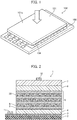
- FIG. 1 is a perspective view of an infrared image capture device including the infrared sensor according to the present embodiment. As illustrated in FIG. 1 , an infrared image capture device 100 includes an infrared sensor 101 and a circuit board 102.
- the infrared sensor 101 is provided on the circuit board 102 by flip-chip bonding through a plurality of bumps 104.
- the infrared sensor 101 includes a quantum dot infrared photo-detector (QDIP) array in which a plurality of pixels are arranged.
- QDIP quantum dot infrared photo-detector
- the bump 104 is provided for each pixel. Note that in the present embodiment, the number of pixels is not limited to a particular value.
- a surface 101a of the infrared sensor 101 illustrated in FIG. 1 is a light reception surface.
- an infrared ray is delivered to the surface 101a from a direction of an arrow, carriers confined in the quantum dot in the infrared sensor 101 are excited and the infrared ray is detected as photocurrent on the circuit board 102 side.
- an image sensor that can detect an infrared ray can be achieved.
- the application of the infrared image capture device 100 in the present embodiment is not limited in particular; however, the infrared image capture device 100 in the present embodiment can be used for a night vision device, a heat source searching device, a security device, or a medical equipment, for example.
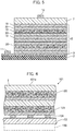
- FIG. 2 is a partial cross-sectional view of the infrared sensor according to the present embodiment.
- an infrared sensor 1 has a stack structure including, for example, a semi-insulating substrate 2, a first electrode formation layer 3, a first spacer layer 4, a light absorption layer 5, a second spacer layer 6, and a second electrode formation layer 7 in this order from the bottom.
- the light absorption layer 5 has a structure in which intermediate layers 8 and quantum dot layers 9 are stacked alternately.
- the quantum dot layers 9 are formed as a plurality of layers in FIG. 2
- the quantum dot layer 9 may be a single layer as illustrated in FIG. 3 .
- the intermediate layer 8 has a wider band gap than a quantum dot 20 included in the quantum dot layer 9.
- the quantum dot layer 9 is held between the intermediate layers 8 on the upper and lower sides.
- Al y Ga 1-y As (0 ⁇ y ⁇ 1) can be used but the material is not limited thereto.
- Al z Ga 1-z As (0 ⁇ z ⁇ 1) can be used.
- the intermediate layer 8 and the spacer layers 4 and 6 are formed of the same material, the intermediate layer 8 and the spacer layers 4 and 6 that are adjacent to each other may be formed as a single layer instead of a two-layer structure.
- the semi-insulating substrate 2 for example, a semi-insulating GaAs substrate can be used.
- the first electrode formation layer 3 of n-type GaAs can be formed by being doped with Si.
- an emitter electrode 11 is provided and on a surface of the second electrode formation layer 7, a collector electrode 12 is provided.
- the application of the voltage makes the emitter electrode 11 higher than the collector electrode 12 in terms of energy.
- a slope electric field is formed in the light absorption layer 5.
- the electrons bound in the quantum level on the conduction band side of the quantum dot are excited and released.
- the released electrons move to the collector electrode 12 by the electric field and form photocurrent.
- a plurality of spherical quantum dots 20 are dispersedly disposed in the quantum dot layer 9.
- the term "spherical” is not limited to the true spherical shape and indicates a shape with a sphericity of 0.7 or more, preferably 0.8 or more, and more preferably 0.9 or more.
- the method of measuring the sphericity for example, image processing is performed using an electron microscope and from the area and the circumferential length of the observed quantum dot, the sphericity can be calculated by 4 ⁇ ⁇ (area)/(circumferential length) 2 .
- the shape with an aspect ratio, which is expressed by major axis/minor axis of the observed quantum dot, of 1.5 or less, preferably 1.3 or less, and more preferably 1.2 or less is defined as being "spherical".
- the quantum dot 20 can be formed by liquid-phase synthesis.
- the quantum dot 20 according to the present embodiment is preferably spherical as described above; however, the quantum dot 20 is not limited to this shape.
- the quantum dot 20 synthesized by the liquid-phase synthesis method has the spherical shape as described above or may have other shape than the spherical shape.
- Other examples of the shape that is not spherical include a stick-like shape and a branch-like shape.
- a resin composition in which the spherical quantum dots 20 are dispersed in resin, and the intermediate layers 8 can be applied alternately and formed.
- the resin in which the quantum dots 20 are dispersed is not limited to particular resin, the following resin can be used: polypropylene, polyethylene, polystyrene, AS resin, ABS resin, methacrylic resin, polyvinyl chloride, polyacetal, polyamide, polycarbonate, modified polyphenylene ether, polybutylene terephthalate, polyethylene terephthalate, polysulfone, polyether sulfone, polyphenylene sulfide, polyamide imide, polymethyl pentene, liquid crystal polymer, epoxy resin, phenol resin, urea resin, melamine resin, diallyl phthalate resin, unsaturated polyester resin, polyimide, polyurethane, silicone resin, cyclic olefin polymer (COP), cyclic olefin copolymer (COC),
- the spherical quantum dots 20 that are dissolved in a solvent can be applied by an inkjet method.
- the quantum dot layer 9 after the drying is mostly formed of the spherical quantum dots 20 and in this quantum dot layer 9, a small amount of solvent component may be left.
- the quantum dot 20 has an emission wavelength of about 800 nm to 1600 nm.
- the quantum dot 20 with such an emission wavelength at least one kind of the following is preferably included: PbS, PbSe, CdHgTe, Ag 2 S, Ag 2 Se, Ag 2 Te, AgInSe 2 , AgInTe 2 , CuInSe 2 , CuInTe 2 , or InAs.
- Ag 2 S does not correspond to RoHS.
- PbS has been reported in the paper of 2003 WILEY-VCH Verlag GmbH & Co. KGaA. Weinheim. ADVANCED MATERIALS 2003, 15. NO. 21 November 4 .
- Ag 2 S has been reported in the paper of ACS NANO VOL. 6 NO. 5 P3695-3702 (2012 ).
- PbS or Ag 2 S is preferably used as the quantum dot 20.
- Ag 2 S, Ag 2 Se, Ag 2 Te, AgInSe 2 , or AgInTe 2 is preferably used as the quantum dot 20.
- the fluorescence half-width in a near-infrared region can be narrowed and near-infrared fluorescence with high luminance can be exhibited.
- one kind, or two or more kinds of quantum dots 20 may be used. That is to say, as the quantum dots 20, either the same kind of quantum dots or different kinds of quantum dots may be used.
- the quantum dot 20 in the present embodiment is a nanoparticle with a particle diameter of about several nanometers to several tens of nanometers, for example.
- a number of organic ligands 21 are coordinated on a surface of the quantum dot 20.
- the aggregation between the quantum dots 20 can be suppressed and the intended optical characteristic can be obtained.
- the ligand that can be used in the reaction is not limited to a particular ligand and for example, the following ligands are given as typical examples.
- Oleylamines C 18 H 35 NH 2
- stearyl (octadecyl) amine C 18 H 37 NH 2
- dodecyl (lauryl) amine C 12 H 25 NH 2
- decylamine C 10 H 21 NH 2
- octylamine C 8 H 17 NH 2
- Oleic acid C 17 H 33 COOH
- stearic acid C 17 H 35 COOH
- palmitic acid C 15 H 31 COOH
- myristic acid C 13 H 27 COOH
- lauric acid C 11 H 23 COOH
- decanoic acid C 9 H 19 COOH
- octanoic acid C 7 H 15 COOH
- Octadecane thiol C 18 H 37 SH, hexanedecane thiol: C 16 H 33 SH, tetradecane thiol: C 14 H 29 SH, dodecane thiol: C 12 H 25 SH, decane thiol: C 10 H 21 SH, octane thiol: C 8 H 17 SH
- Trioctyl phosphine (C 8 H 17 ) 3 P
- triphenyl phosphine (C 6 H 5 ) 3 P
- tributyl phosphine (C 4 H 9 ) 3 P
- the organic ligand 21 it is preferable to use a short ligand as the organic ligand 21.
- the ligand is not limited to a particular ligand, 3-mercaptopropionic acid (MPA) can be used as the organic ligand 21.
- MPA 3-mercaptopropionic acid
- the ligand of the quantum dot 20 included in the quantum dot layer 9 is preferably shorter than the ligand when the quantum dot 20 is formed by the liquid-phase synthesis method.
- the roughness of the quantum dot layer 9 can be reduced and the electrons and holes can be extracted with higher efficiency.
- the dispersion film forming property can be improved.
- the synthesis of the quantum dot 20 with the long ligand by the liquid-phase synthesis method may be followed by the replacement of the composition including the quantum dot 20 with a short ligand (for example, 3-mercaptopropionic acid) after or before the application.
- a short ligand for example, 3-mercaptopropionic acid
- the quantum dot 20 may have a core-shell structure including a core 20a and a shell 20b that covers a surface of the core 20a. It is preferable that a number of organic ligands 21 are coordinated on the surface of the quantum dot 20 as illustrated in FIG. 4B .
- the organic ligand 21 is as already described above.
- the core 20a of the quantum dot 20 illustrated in FIG. 4B is a nanoparticle illustrated in FIG. 3A . Therefore, the core 20a is formed of the material of the quantum dot 20 described above, for example.
- the shell 20b may exist as a solid solution on the surface of the core 20a.
- the border between the core 20a and the shell 20b is shown by a dotted line, and this means that the border between the core 20a and the shell 20b may be either recognizable or not by the analysis.
- the infrared sensor 1 illustrated in FIG. 2 is inverted to form the infrared sensor (QDIP array) 101 whose semi-insulating substrate 2 side faces upward.
- This infrared sensor 101 is electrically connected onto the circuit board 102 through the bump 104 illustrated in FIG. 1 .
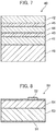
- FIG. 5 is a partial sectional view of the infrared sensor according to the present embodiment, which is partially different from FIG. 2 .
- the infrared sensor illustrated in FIG. 5 has a stack structure including the semi-insulating substrate 2, the first electrode formation layer 3, a light absorption layer 15, and the second electrode formation layer 7 in this order from the bottom.
- the light absorption layer 15 has a stack structure including an intermediate layer 18/a barrier layer 30/a quantum dot layer 19/the barrier layer 30/the intermediate layer 18.
- the potential to the carrier in the barrier layer 30 is higher than the potential to the carrier in the intermediate layer 18.
- the potential to the carrier in the quantum dot 20 included in the quantum dot layer 19 is lower than the potential to the carrier in the intermediate layer 18.
- the potential to the carrier in the quantum dot 20 is lower than the potential to the carrier in the barrier layer 30.
- the band gap of the barrier layer 30 is larger than the band gap of the intermediate layer 18.
- the band gap of the quantum dot 20 is smaller than the band gap of each of the intermediate layer 18 and the barrier layer 30.
- the quantum dot 20 included in the light absorption layer 15 of the infrared sensor illustrated in FIG. 5 is spherical. It is preferable that the quantum dot 20 includes at least one kind of PbS, PbSe, CdHgTe, Ag 2 S, Ag 2 Se, Ag 2 Te, AgInSe 2 , AgInTe 2 , CuInSe 2 , CuInTe 2 , and InAs.
- the infrared sensor illustrated in FIG. 5 is inverted to form the infrared sensor (QDIP array) 101 whose semi-insulating substrate 2 side faces upward.
- This infrared sensor 101 is electrically connected onto the circuit board 102 through the bump 104 illustrated in FIG. 1 .
- the stack structure illustrated in FIG. 2 and FIG. 5 may be formed in a manner of being divided for each pixel.
- the layers can be divided into two or more regions of a far-infrared region that detects a far-infrared ray, a middle-infrared region that detects a middle-infrared ray, and a near-infrared region that detects a near-infrared ray.
- the long-wavelength region is disposed on the semi-insulating substrate 2 side, that is, on the light reception surface side.
- the quantum dot layer including the quantum dot with an emission wavelength in the middle-infrared region is formed in the quantum dot layer with the middle-infrared region
- the quantum dot layer including the quantum dot with an emission wavelength in the near-infrared region is formed in the quantum dot layer with the near-infrared region.
- FIG. 6 is a magnified cross-sectional view of a part of the infrared image capture device including the infrared sensor according to the present embodiment.
- the infrared sensor 101 includes an infrared detection layer 120 that detects the infrared ray, and a visible light detection layer 121 that detects visible light.
- the structure of the infrared detection layer 120 illustrated in FIG. 6 is the stack structure illustrated in FIG. 2 and FIG. 5 .
- the quantum dot that is used is spherical and includes at least one kind of PbS, PbSe, CdHgTe, Ag 2 S, Ag 2 Se, Ag 2 Te, AgInSe 2 , AgInTe 2 , CuInSe 2 , CuInTe 2 , and InAs.
- a quantum dot with an emission wavelength in a visible light region is employed as the quantum dot used in the visible light detection layer 121.
- the quantum dot in the present embodiment is a nanoparticle with a particle diameter of several nanometers to several tens of nanometers.
- the quantum dot employed in the visible light region is formed of, for example, CdS-based, CdSe-based, ZnS-based, ZnSe-based, ZnSeS-based, ZnTe-based, ZnTeS-based, InP-based, or chalcopyrite-based (CuInS-based, AgInS-based) quantum dot.
- the structure of the quantum dot used in the visible light detection layer 121 may be the structure including the core alone as illustrated in FIG. 4A or the core-shell structure as illustrated in FIG. 4B .
- the infrared sensor 101 in FIG. 6 By using the infrared sensor 101 in FIG. 6 , not just the infrared ray but also visible light can be detected.
- the place to install the cooling device 130 is not limited to a particular place and may be any place where the quantum dot layer can be cooled properly.
- the infrared sensor including the quantum dots according to the present embodiment can confine the carriers firmly, and has the excellent sensitivity to vertical incident light; thus, this infrared sensor is expected as an infrared detector with high sensitivity and low dark current.
- the quantum dot layer has conventionally been micro-processed into the island shape. Therefore, the adjustment for the micro-processing is necessary and the manufacturing process becomes complicated easily. In addition, the manufacturing cost easily increases.
- the present embodiment provides the structure in which the spherical quantum dot is applied and the micro-processing that has been performed conventionally is no longer necessary; thus, the conventional problem does not occur. Furthermore, for example, the quantum dot formed by the liquid-phase synthesis method (particularly, spherical quantum dot) is used; therefore, the quantum dot has excellent sensitivity in all directions and the variation in sensitivity can be reduced as compared to the conventional micro-processed quantum dot.
- the quantum dot it is preferable to include at least one kind of PbS, PbSe, CdHgTe, Ag 2 S, Ag 2 Se, Ag 2 Te, AgInSe 2 , AgInTe 2 , CuInSe 2 , CuInTe 2 , and InAs as the quantum dot.
- These elements have an emission wavelength of 800 nm to 1600 nm, and are suitably used for the infrared sensor.
- the infrared sensor according to the present embodiment is used for, for example, a photoelectric element or a thermoelectric element that is described below.
- FIG. 7 and FIG. 8 are partial sectional views each illustrating an example of a photoelectric conversion element according to the present embodiment.
- a photoelectric conversion element 40 illustrated in FIG. 7 includes a first conductive layer 41 that is a cathode and a second conductive layer 42 that is an anode, and also includes an electron transportation layer 43, a light absorption layer 44, and a hole transportation layer 45 between the first conductive layer 41 and the second conductive layer 42.
- the first conductive layer 41 is formed on a glass substrate 46.
- the light absorption layer 44 is a layer that absorbs light having entered the photoelectric conversion element 40 and generates electrons and holes, and includes the aforementioned spherical quantum dot.
- a photoelectric conversion element (PN-type photodiode) 50 illustrated in FIG. 8 includes a P-type semiconductor layer 53 and an N-type semiconductor layer 54 between a first electrode 51 and a second electrode 52.
- the structure includes the electrodes 51 and 52 in the semiconductor with the PN junction, which is similar to a solar cell.
- the n-type semiconductor includes many electrons that move easily, and some electrons move to the p-type semiconductor to be combined with the holes to cancel the charges, so that a region called a depletion layer is formed. In the n-type semiconductor in the depletion layer, the electrons disappear so that this region is charged to become positive and in the p-type semiconductor, the holes disappear so that this region is charged to become negative; thus, an internal electric field is generated.
- the device with the PN junction can be formed in a manner that the spherical quantum dot formed of InAs, which easily becomes p-ch, is used for the P-type semiconductor layer 53 and the spherical quantum dot formed of Ag 2 Te, which easily becomes n-ch, is used for the N-type semiconductor layer 54.
- the infrared sensor is usable in an image capture device, the medical field, the communication field, the solar cell, or the like.
- the energy level diagram is as shown in any of FIG. 9A to FIG. 9D .
- the shell of the core-shell structure is important in improving the quantum confining effect.
- a type-I structure illustrated in FIG. 9A (the LUMO of the shell has higher energy than the LUMO of the core, and the HOMO of the shell has lower energy than the HOMO of the core) is preferable.
- type-II structures are preferable because the carriers (electrons, holes) are easily extracted.
- the hole mobility is lower than the electron mobility, it is preferable to select the type 11(1) or the type 11(3).
- the quantum dot with the core structure including the ligand can be used instead of the core-shell structure.
- the LUMO of the shell has lower energy than the LUMO of the core and the HOMO of the shell has higher energy than the HOMO of the core.
- the type-II(3) the LUMO of the shell has higher energy than the LUMO of the core and the HOMO of the shell has higher energy than the HOMO of the core.
- a manufacturing method for the infrared sensor according to the present embodiment includes a step of forming the spherical quantum dot by the liquid-phase synthesis method, and a step of forming the light absorption layer by applying the composition including a plurality of the quantum dots.
- each element source forming the quantum dot is dissolved in a solvent and a precursor solution including each element is subjected to reaction using, for example, a microreactor; thus, the quantum dot particle including a predetermined element can be synthesized.
- the spherical quantum dot can be obtained.
- the quantum dot including the ligand with the long chain is preferably used in the application; however, in the manufacture of the device, a ligand with a short chain is preferable in order to extract the carriers (electrons and holes) with higher efficiency.
- the number of carbons of the ligand with the short chain may be 2 to 5 (preferably 2 to 3) and for example, 3-mercaptopropionic acid can be used as the ligand with the short chain.
- the ligand of the quantum dot can be replaced by the shorter ligand.
- a composition including the quantum dot (including quantum dot and solvent) is applied using a spin coater. Since the ligand with the long chain is dispersed more, a film with superior roughness can be formed; however, the ligand with the long chain is disadvantageous in terms of carrier extraction. Therefore, for example, after the application, the ligand with the short chain is dropped on the applied film. Accordingly, the ligand with the long chain is replaced by the ligand with the short chain naturally and then, the ligand with the long chain is washed off by cleaning.
- the ligand with the long chain can be replaced by the ligand with the short chain and then, a composition including the quantum dot (the composition may be a resin composition) can be applied.
- the infrared ray can be detected in the present invention.
- the infrared sensor according to the present invention is applicable to a night vision device, a heat source searching device, a security device, or a medical equipment, for example.
Landscapes
- Physics & Mathematics (AREA)
- General Physics & Mathematics (AREA)
- Spectroscopy & Molecular Physics (AREA)
- Light Receiving Elements (AREA)
- Photometry And Measurement Of Optical Pulse Characteristics (AREA)
- Chemical & Material Sciences (AREA)
- Engineering & Computer Science (AREA)
- Nanotechnology (AREA)
- Encapsulation Of And Coatings For Semiconductor Or Solid State Devices (AREA)
Abstract
Description
- The present invention relates to an infrared sensor capable of detecting an infrared ray, and a manufacturing method for the same.
-
Patent Literature 1 below has disclosed the invention about a quantum dot type infrared detector. The infrared detector according toPatent Literature 1 includes a stack structure including a quantum dot layer including a plurality of quantum dots and intermediate layers having the quantum dot layer held therebetween. - According to
Patent Literature 1, the quantum dots are micro-processed into an island shape. The quantum dots are formed of InAs. - [Patent Literature 1]
Japanese Laid-Open Patent Publication No. 2015-162478 - However, the infrared sensor in which the quantum dots are micro-processed into the island shape as described in
Patent Literature 1 easily causes problems that adjustment for the micro-processing or the manufacturing process becomes complicated and moreover, the manufacturing cost increases. - In addition, depending on the growing degree of the quantum dots that are micro-processed into the island shape, for example, the decrease in sensitivity or variation has been concerned.
- The present invention has been made in view of such circumstances, and an object is to provide an infrared sensor with the quantum dots optimized, and a manufacturing method for the same.
- The present invention provides an infrared sensor including a light absorption layer that absorbs an infrared ray, wherein the light absorption layer includes a plurality of quantum dots, and the quantum dot is spherical.
- In addition, the present invention provides a manufacturing method for an infrared sensor including a light absorption layer that absorbs an infrared ray. The manufacturing method includes a step of forming a quantum dot by a liquid-phase synthesis method, and a step of forming the light absorption layer by applying a composition including a plurality of the quantum dots.
- In the infrared sensor according to the present invention, the structure of the light absorption layer including the quantum dot can be optimized.
-
-
FIG. 1 is a perspective view of an infrared image capture device including an infrared sensor according to the present embodiment; -
FIG. 2 is a partial cross-sectional view of the infrared sensor according to the present embodiment; -
FIG. 3 is a partial cross-sectional view of the infrared sensor according to the present embodiment that is partially different fromFIG. 2 ; -
FIG. 4a and FIG. 4b are a schematic view of a quantum dot in the present embodiment; -
FIG. 5 is a partial cross-sectional view of the infrared sensor according to the present embodiment that is partially different fromFIG. 2 ; -
FIG. 6 is a magnified cross-sectional view of a part of the infrared image capture device including the infrared sensor according to the present embodiment; -
FIG. 7 is a partial cross-sectional view illustrating one example of a photoelectric conversion element according to the present embodiment; -
FIG. 8 is a partial cross-sectional view illustrating one example of the photoelectric conversion element according to the present embodiment; and -
FIG. 9a to FIG. 9D are an energy level diagram in a case where a quantum dot with a core-shell structure is used. - One embodiment of the present invention (hereinafter referred to as "embodiment" simply) is hereinafter described in detail. Note that the present invention is not limited to the embodiment below, and various changes are possible within the range of the concept thereof.
- Conventionally, in an infrared sensor including a light absorption layer including quantum dots, the light absorption layer is formed by micro-processing the quantum dots into an island shape through a micro-processing technique, for example, by epitaxial growth of the quantum dots. This structure, however, has problems that the roughness of the light absorption layer easily increases and the variation in sensitivity or the decrease in sensitivity is caused. In view of this, as a result of eager studies, the present inventors have developed an infrared sensor capable of suppressing the variation in sensitivity and improving the sensitivity by forming the quantum dots included in the light absorption layer into a spherical shape by a liquid-phase synthesis method, for example, without using the aforementioned micro-processing technique. A structure of the infrared sensor according to the present embodiment is described below.
-
FIG. 1 is a perspective view of an infrared image capture device including the infrared sensor according to the present embodiment. As illustrated inFIG. 1 , an infraredimage capture device 100 includes aninfrared sensor 101 and acircuit board 102. - As illustrated in
FIG. 1 , theinfrared sensor 101 is provided on thecircuit board 102 by flip-chip bonding through a plurality ofbumps 104. - For example, the
infrared sensor 101 includes a quantum dot infrared photo-detector (QDIP) array in which a plurality of pixels are arranged. Thebump 104 is provided for each pixel. Note that in the present embodiment, the number of pixels is not limited to a particular value. - A
surface 101a of theinfrared sensor 101 illustrated inFIG. 1 is a light reception surface. When an infrared ray is delivered to thesurface 101a from a direction of an arrow, carriers confined in the quantum dot in theinfrared sensor 101 are excited and the infrared ray is detected as photocurrent on thecircuit board 102 side. - In the present embodiment, an image sensor that can detect an infrared ray can be achieved. The application of the infrared
image capture device 100 in the present embodiment is not limited in particular; however, the infraredimage capture device 100 in the present embodiment can be used for a night vision device, a heat source searching device, a security device, or a medical equipment, for example. -
FIG. 2 is a partial cross-sectional view of the infrared sensor according to the present embodiment. As illustrated inFIG. 2 , aninfrared sensor 1 has a stack structure including, for example, asemi-insulating substrate 2, a firstelectrode formation layer 3, afirst spacer layer 4, alight absorption layer 5, asecond spacer layer 6, and a secondelectrode formation layer 7 in this order from the bottom. - As illustrated in
FIG. 2 , thelight absorption layer 5 has a structure in whichintermediate layers 8 andquantum dot layers 9 are stacked alternately. Although thequantum dot layers 9 are formed as a plurality of layers inFIG. 2 , thequantum dot layer 9 may be a single layer as illustrated inFIG. 3 . - The
intermediate layer 8 has a wider band gap than aquantum dot 20 included in thequantum dot layer 9. Thequantum dot layer 9 is held between theintermediate layers 8 on the upper and lower sides. For example, as theintermediate layer 8, AlyGa1-yAs (0 ≤ y < 1) can be used but the material is not limited thereto. As thespacer layers intermediate layer 8 and thespacer layers intermediate layer 8 and thespacer layers semi-insulating substrate 2, for example, a semi-insulating GaAs substrate can be used. On a surface of the semi-insulating GaAs substrate, for example, the firstelectrode formation layer 3 of n-type GaAs can be formed by being doped with Si. - As illustrated in
FIG. 2 , for example, on a surface of the firstelectrode formation layer 3, anemitter electrode 11 is provided and on a surface of the secondelectrode formation layer 7, acollector electrode 12 is provided. - When the infrared ray is detected, voltage is applied to the
light absorption layer 5 from a power source (not shown) through theemitter electrode 11 and thecollector electrode 12. - The application of the voltage makes the
emitter electrode 11 higher than thecollector electrode 12 in terms of energy. Thus, a slope electric field is formed in thelight absorption layer 5. When the infrared ray has entered thelight absorption layer 5, the electrons bound in the quantum level on the conduction band side of the quantum dot are excited and released. The released electrons move to thecollector electrode 12 by the electric field and form photocurrent. - As illustrated in
FIG. 2 , a plurality of sphericalquantum dots 20 are dispersedly disposed in thequantum dot layer 9. Here, the term "spherical" is not limited to the true spherical shape and indicates a shape with a sphericity of 0.7 or more, preferably 0.8 or more, and more preferably 0.9 or more. As for the method of measuring the sphericity, for example, image processing is performed using an electron microscope and from the area and the circumferential length of the observed quantum dot, the sphericity can be calculated by 4π × (area)/(circumferential length)2. Alternatively, the shape with an aspect ratio, which is expressed by major axis/minor axis of the observed quantum dot, of 1.5 or less, preferably 1.3 or less, and more preferably 1.2 or less is defined as being "spherical". - In the present embodiment, the
quantum dot 20 can be formed by liquid-phase synthesis. Thequantum dot 20 according to the present embodiment is preferably spherical as described above; however, thequantum dot 20 is not limited to this shape. Thequantum dot 20 synthesized by the liquid-phase synthesis method has the spherical shape as described above or may have other shape than the spherical shape. Other examples of the shape that is not spherical include a stick-like shape and a branch-like shape. - For example, in the present embodiment, a resin composition in which the
spherical quantum dots 20 are dispersed in resin, and theintermediate layers 8 can be applied alternately and formed. Here, although the resin in which thequantum dots 20 are dispersed is not limited to particular resin, the following resin can be used: polypropylene, polyethylene, polystyrene, AS resin, ABS resin, methacrylic resin, polyvinyl chloride, polyacetal, polyamide, polycarbonate, modified polyphenylene ether, polybutylene terephthalate, polyethylene terephthalate, polysulfone, polyether sulfone, polyphenylene sulfide, polyamide imide, polymethyl pentene, liquid crystal polymer, epoxy resin, phenol resin, urea resin, melamine resin, diallyl phthalate resin, unsaturated polyester resin, polyimide, polyurethane, silicone resin, cyclic olefin polymer (COP), cyclic olefin copolymer (COC), ethylene vinyl alcohol, polymethyl pentene, polyvinylidene fluoride, and the like. - Alternatively, in the present embodiment, the
spherical quantum dots 20 that are dissolved in a solvent can be applied by an inkjet method. In this case, thequantum dot layer 9 after the drying is mostly formed of thespherical quantum dots 20 and in thisquantum dot layer 9, a small amount of solvent component may be left. - The
quantum dot 20 has an emission wavelength of about 800 nm to 1600 nm. As thequantum dot 20 with such an emission wavelength, at least one kind of the following is preferably included: PbS, PbSe, CdHgTe, Ag2S, Ag2Se, Ag2Te, AgInSe2, AgInTe2, CuInSe2, CuInTe2, or InAs. Among these, Ag2S does not correspond to RoHS. Note that PbS has been reported in the paper of 2003 WILEY-VCH Verlag GmbH & Co. KGaA. Weinheim. . In addition, Ag2S has been reported in the paper of ACS NANO VOL. 6 NO. 5 P3695-3702 (2012). - In the present embodiment, PbS or Ag2S is preferably used as the
quantum dot 20. In addition, by using Ag2S, Ag2Se, Ag2Te, AgInSe2, or AgInTe2 as thequantum dot 20, the fluorescence half-width in a near-infrared region can be narrowed and near-infrared fluorescence with high luminance can be exhibited. - In the present embodiment, one kind, or two or more kinds of
quantum dots 20 may be used. That is to say, as thequantum dots 20, either the same kind of quantum dots or different kinds of quantum dots may be used. - The
quantum dot 20 in the present embodiment is a nanoparticle with a particle diameter of about several nanometers to several tens of nanometers, for example. - As illustrated in
FIG. 4A , it is preferable that a number oforganic ligands 21 are coordinated on a surface of thequantum dot 20. In this case, the aggregation between thequantum dots 20 can be suppressed and the intended optical characteristic can be obtained. The ligand that can be used in the reaction is not limited to a particular ligand and for example, the following ligands are given as typical examples. - Oleylamines: C18H35NH2, stearyl (octadecyl) amine: C18H37NH2, dodecyl (lauryl) amine: C12H25NH2, decylamine: C10H21NH2, octylamine: C8H17NH2
- Oleic acid: C17H33COOH, stearic acid: C17H35COOH, palmitic acid: C15H31COOH, myristic acid: C13H27COOH, lauric acid: C11H23COOH, decanoic acid: C9H19COOH, octanoic acid: C7H15COOH
- Octadecane thiol: C18H37SH, hexanedecane thiol: C16H33SH, tetradecane thiol: C14H29SH, dodecane thiol: C12H25SH, decane thiol: C10H21SH, octane thiol: C8H17SH
- Trioctyl phosphine: (C8H17)3P, triphenyl phosphine: (C6H5)3P, tributyl phosphine: (C4H9)3P
- Trioctyl phosphine oxide: (C8H17)3P=O, triphenyl phosphine oxide: (C6H5)3P=O, tributyl phosphine oxide: (C4H9)3P=O
- In the present embodiment, it is preferable to use a short ligand as the
organic ligand 21. Although the ligand is not limited to a particular ligand, 3-mercaptopropionic acid (MPA) can be used as theorganic ligand 21. - The ligand of the
quantum dot 20 included in thequantum dot layer 9 is preferably shorter than the ligand when thequantum dot 20 is formed by the liquid-phase synthesis method. - In this manner, by using the short ligand as the ligand of the
quantum dot 20 included in thequantum dot layer 9, the roughness of thequantum dot layer 9 can be reduced and the electrons and holes can be extracted with higher efficiency. On the other hand, by using the long ligand when thequantum dot 20 is formed by the liquid-phase synthesis method, the dispersion film forming property can be improved. - Alternatively, the synthesis of the
quantum dot 20 with the long ligand by the liquid-phase synthesis method may be followed by the replacement of the composition including thequantum dot 20 with a short ligand (for example, 3-mercaptopropionic acid) after or before the application. - As illustrated in
FIG. 4B , thequantum dot 20 may have a core-shell structure including acore 20a and ashell 20b that covers a surface of thecore 20a. It is preferable that a number oforganic ligands 21 are coordinated on the surface of thequantum dot 20 as illustrated inFIG. 4B . Theorganic ligand 21 is as already described above. The core 20a of thequantum dot 20 illustrated inFIG. 4B is a nanoparticle illustrated inFIG. 3A . Therefore, thecore 20a is formed of the material of thequantum dot 20 described above, for example. - Note that the
shell 20b may exist as a solid solution on the surface of thecore 20a. InFIG. 4B , the border between the core 20a and theshell 20b is shown by a dotted line, and this means that the border between the core 20a and theshell 20b may be either recognizable or not by the analysis. - The
infrared sensor 1 illustrated inFIG. 2 is inverted to form the infrared sensor (QDIP array) 101 whosesemi-insulating substrate 2 side faces upward. Thisinfrared sensor 101 is electrically connected onto thecircuit board 102 through thebump 104 illustrated inFIG. 1 . -
FIG. 5 is a partial sectional view of the infrared sensor according to the present embodiment, which is partially different fromFIG. 2 . The infrared sensor illustrated inFIG. 5 has a stack structure including thesemi-insulating substrate 2, the firstelectrode formation layer 3, alight absorption layer 15, and the secondelectrode formation layer 7 in this order from the bottom. - In
FIG. 5 , thelight absorption layer 15 has a stack structure including anintermediate layer 18/abarrier layer 30/aquantum dot layer 19/thebarrier layer 30/theintermediate layer 18. - Here, the potential to the carrier in the
barrier layer 30 is higher than the potential to the carrier in theintermediate layer 18. In addition, the potential to the carrier in thequantum dot 20 included in thequantum dot layer 19 is lower than the potential to the carrier in theintermediate layer 18. The potential to the carrier in thequantum dot 20 is lower than the potential to the carrier in thebarrier layer 30. The band gap of thebarrier layer 30 is larger than the band gap of theintermediate layer 18. In addition, the band gap of thequantum dot 20 is smaller than the band gap of each of theintermediate layer 18 and thebarrier layer 30. - In a manner similar to
FIG. 2 , thequantum dot 20 included in thelight absorption layer 15 of the infrared sensor illustrated inFIG. 5 is spherical. It is preferable that thequantum dot 20 includes at least one kind of PbS, PbSe, CdHgTe, Ag2S, Ag2Se, Ag2Te, AgInSe2, AgInTe2, CuInSe2, CuInTe2, and InAs. - In a manner similar to
FIG. 2 , the infrared sensor illustrated inFIG. 5 is inverted to form the infrared sensor (QDIP array) 101 whosesemi-insulating substrate 2 side faces upward. Thisinfrared sensor 101 is electrically connected onto thecircuit board 102 through thebump 104 illustrated inFIG. 1 . - The stack structure illustrated in
FIG. 2 andFIG. 5 may be formed in a manner of being divided for each pixel. - As illustrated in
FIG. 2 andFIG. 5 , in the structure where the plurality ofquantum dot layers semi-insulating substrate 2 side, that is, on the light reception surface side. For example, the quantum dot layer including the quantum dot with an emission wavelength in the middle-infrared region is formed in the quantum dot layer with the middle-infrared region, and the quantum dot layer including the quantum dot with an emission wavelength in the near-infrared region is formed in the quantum dot layer with the near-infrared region. -
FIG. 6 is a magnified cross-sectional view of a part of the infrared image capture device including the infrared sensor according to the present embodiment. - In
FIG. 6 , theinfrared sensor 101 includes aninfrared detection layer 120 that detects the infrared ray, and a visiblelight detection layer 121 that detects visible light. - The structure of the
infrared detection layer 120 illustrated inFIG. 6 is the stack structure illustrated inFIG. 2 andFIG. 5 . In this structure, it is preferable that the quantum dot that is used is spherical and includes at least one kind of PbS, PbSe, CdHgTe, Ag2S, Ag2Se, Ag2Te, AgInSe2, AgInTe2, CuInSe2, CuInTe2, and InAs. - On the other hand, a quantum dot with an emission wavelength in a visible light region is employed as the quantum dot used in the visible
light detection layer 121. - Although the structure and the material of the quantum dot are not limited in particular, for example, the quantum dot in the present embodiment is a nanoparticle with a particle diameter of several nanometers to several tens of nanometers.
- The quantum dot employed in the visible light region is formed of, for example, CdS-based, CdSe-based, ZnS-based, ZnSe-based, ZnSeS-based, ZnTe-based, ZnTeS-based, InP-based, or chalcopyrite-based (CuInS-based, AgInS-based) quantum dot.
- Note that the structure of the quantum dot used in the visible
light detection layer 121 may be the structure including the core alone as illustrated inFIG. 4A or the core-shell structure as illustrated inFIG. 4B . - By using the
infrared sensor 101 inFIG. 6 , not just the infrared ray but also visible light can be detected. - By cooling the quantum dot, the thermal noise can be reduced and the sensitivity can be improved. Therefore, it is preferable to install a
cooling device 130 as illustrated inFIG. 6 . The place to install thecooling device 130 is not limited to a particular place and may be any place where the quantum dot layer can be cooled properly. - The infrared sensor including the quantum dots according to the present embodiment can confine the carriers firmly, and has the excellent sensitivity to vertical incident light; thus, this infrared sensor is expected as an infrared detector with high sensitivity and low dark current.
- Incidentally, the quantum dot layer has conventionally been micro-processed into the island shape. Therefore, the adjustment for the micro-processing is necessary and the manufacturing process becomes complicated easily. In addition, the manufacturing cost easily increases.
- On the other hand, the present embodiment provides the structure in which the spherical quantum dot is applied and the micro-processing that has been performed conventionally is no longer necessary; thus, the conventional problem does not occur. Furthermore, for example, the quantum dot formed by the liquid-phase synthesis method (particularly, spherical quantum dot) is used; therefore, the quantum dot has excellent sensitivity in all directions and the variation in sensitivity can be reduced as compared to the conventional micro-processed quantum dot.
- In the present embodiment, it is preferable to include at least one kind of PbS, PbSe, CdHgTe, Ag2S, Ag2Se, Ag2Te, AgInSe2, AgInTe2, CuInSe2, CuInTe2, and InAs as the quantum dot. These elements have an emission wavelength of 800 nm to 1600 nm, and are suitably used for the infrared sensor.
- In addition, the infrared sensor according to the present embodiment is used for, for example, a photoelectric element or a thermoelectric element that is described below.
-
FIG. 7 and FIG. 8 are partial sectional views each illustrating an example of a photoelectric conversion element according to the present embodiment. Aphotoelectric conversion element 40 illustrated inFIG. 7 includes a firstconductive layer 41 that is a cathode and a secondconductive layer 42 that is an anode, and also includes anelectron transportation layer 43, alight absorption layer 44, and ahole transportation layer 45 between the firstconductive layer 41 and the secondconductive layer 42. For example, the firstconductive layer 41 is formed on aglass substrate 46. - For the
electron transportation layer 43, ZnO that easily becomes n-ch is preferably used. Thelight absorption layer 44 is a layer that absorbs light having entered thephotoelectric conversion element 40 and generates electrons and holes, and includes the aforementioned spherical quantum dot. - A photoelectric conversion element (PN-type photodiode) 50 illustrated in
FIG. 8 includes a P-type semiconductor layer 53 and an N-type semiconductor layer 54 between afirst electrode 51 and asecond electrode 52. In this manner, the structure includes theelectrodes type semiconductor layer 53 and the spherical quantum dot formed of Ag2Te, which easily becomes n-ch, is used for the N-type semiconductor layer 54. - In the present embodiment, the infrared sensor is usable in an image capture device, the medical field, the communication field, the solar cell, or the like.
- In a case where the quantum dot employed in the present embodiment has the core-shell structure, the energy level diagram is as shown in any of
FIG. 9A to FIG. 9D . Here, in the case of a light-emitting element, the shell of the core-shell structure is important in improving the quantum confining effect. In particular, a type-I structure illustrated inFIG. 9A (the LUMO of the shell has higher energy than the LUMO of the core, and the HOMO of the shell has lower energy than the HOMO of the core) is preferable. - On the other hand, in the case of using the quantum dot in the photoelectric conversion element, type-II structures are preferable because the carriers (electrons, holes) are easily extracted. In general, since the hole mobility is lower than the electron mobility, it is preferable to select the type 11(1) or the type 11(3). Note that, in the case of using the quantum dot in the photoelectric conversion element, the quantum dot with the core structure including the ligand can be used instead of the core-shell structure. In the type-II(1), the LUMO of the shell has lower energy than the LUMO of the core and the HOMO of the shell has higher energy than the HOMO of the core. In the type-II(3), the LUMO of the shell has higher energy than the LUMO of the core and the HOMO of the shell has higher energy than the HOMO of the core.
- A manufacturing method for the infrared sensor according to the present embodiment includes a step of forming the spherical quantum dot by the liquid-phase synthesis method, and a step of forming the light absorption layer by applying the composition including a plurality of the quantum dots.
- In the present embodiment, as the liquid-phase synthesis method, each element source forming the quantum dot is dissolved in a solvent and a precursor solution including each element is subjected to reaction using, for example, a microreactor; thus, the quantum dot particle including a predetermined element can be synthesized. Thus, the spherical quantum dot can be obtained.
- In order to disperse the quantum dots more, it is preferable to use a ligand with a long chain. For this purpose, the quantum dot including the ligand with the long chain is preferably used in the application; however, in the manufacture of the device, a ligand with a short chain is preferable in order to extract the carriers (electrons and holes) with higher efficiency. Although not limited, the number of carbons of the ligand with the short chain may be 2 to 5 (preferably 2 to 3) and for example, 3-mercaptopropionic acid can be used as the ligand with the short chain.
- In the present embodiment, after the quantum dot is synthesized by the liquid-phase synthesis method, the ligand of the quantum dot can be replaced by the shorter ligand. For example, a composition including the quantum dot (including quantum dot and solvent) is applied using a spin coater. Since the ligand with the long chain is dispersed more, a film with superior roughness can be formed; however, the ligand with the long chain is disadvantageous in terms of carrier extraction. Therefore, for example, after the application, the ligand with the short chain is dropped on the applied film. Accordingly, the ligand with the long chain is replaced by the ligand with the short chain naturally and then, the ligand with the long chain is washed off by cleaning. Alternatively, after the quantum dot is synthesized by the liquid-phase synthesis method and before the application, the ligand with the long chain can be replaced by the ligand with the short chain and then, a composition including the quantum dot (the composition may be a resin composition) can be applied.
- The infrared ray can be detected in the present invention. The infrared sensor according to the present invention is applicable to a night vision device, a heat source searching device, a security device, or a medical equipment, for example.
- This application is based upon
Japanese Patent Application No. 2018-170491 filed on September 12, 2018
Claims (9)
- An infrared sensor comprising a light absorption layer that absorbs an infrared ray, wherein
the light absorption layer includes a plurality of quantum dots, and
the quantum dot is spherical. - An infrared sensor comprising a light absorption layer that absorbs an infrared ray, wherein
the light absorption layer includes a plurality of quantum dots, and
the quantum dot includes at least one kind of PbS, PbSe, CdHgTe, Ag2S, Ag2Se, Ag2Te, AgInSe2, AgInTe2, CuInSe2, CuInTe2, and InAs. - An infrared sensor comprising a light absorption layer that absorbs an infrared ray, wherein
the light absorption layer includes a plurality of quantum dots, and
the quantum dot is formed by liquid-phase synthesis. - The infrared sensor according to claim 2 or 3, wherein the quantum dot is spherical.
- The infrared sensor according to any of claims 1 to 4, wherein a quantum dot layer including the quantum dots is formed by application.
- The infrared sensor according to any of claims 1 to 5, wherein a ligand of the quantum dot included in the light absorption layer is shorter than the ligand of the quantum dot that is formed by the liquid-phase synthesis.
- The infrared sensor according to any of claims 1 to 6, wherein the infrared sensor includes a photoelectric element or a thermoelectric element.
- A manufacturing method for an infrared sensor including a light absorption layer that absorbs an infrared ray, the manufacturing method comprising:a step of forming a quantum dot by a liquid-phase synthesis method; anda step of forming the light absorption layer by applying a composition including a plurality of the quantum dots.
- The manufacturing method for an infrared sensor according to claim 8, wherein after the quantum dot is synthesized by the liquid-phase synthesis method, a ligand of the quantum dot is replaced by a shorter ligand.
Applications Claiming Priority (2)
| Application Number | Priority Date | Filing Date | Title |
|---|---|---|---|
| JP2018170491 | 2018-09-12 | ||
| PCT/JP2019/035713 WO2020054764A1 (en) | 2018-09-12 | 2019-09-11 | Infrared sensor and method for producing same |
Publications (2)
| Publication Number | Publication Date |
|---|---|
| EP3852151A1 true EP3852151A1 (en) | 2021-07-21 |
| EP3852151A4 EP3852151A4 (en) | 2022-06-15 |
Family
ID=69778412
Family Applications (1)
| Application Number | Title | Priority Date | Filing Date |
|---|---|---|---|
| EP19859093.7A Pending EP3852151A4 (en) | 2018-09-12 | 2019-09-11 | INFRARED SENSOR AND METHOD FOR PRODUCTION |
Country Status (7)
| Country | Link |
|---|---|
| US (2) | US12266734B2 (en) |
| EP (1) | EP3852151A4 (en) |
| JP (1) | JPWO2020054764A1 (en) |
| KR (2) | KR102732888B1 (en) |
| CN (1) | CN112703609A (en) |
| TW (2) | TWI902020B (en) |
| WO (1) | WO2020054764A1 (en) |
Families Citing this family (14)
| Publication number | Priority date | Publication date | Assignee | Title |
|---|---|---|---|---|
| TWI807531B (en) * | 2021-01-06 | 2023-07-01 | 日商田中貴金屬工業股份有限公司 | Photoelectric conversion element material, production method of photoelectric conversion element material, and ink with semiconductor nanoparticles dispersed therein |
| US20240188317A1 (en) * | 2021-03-30 | 2024-06-06 | Sharp Kabushiki Kaisha | Light emitting element, display device, manufacturing method of light emitting element, and manufacturing method of display device |
| TW202312476A (en) * | 2021-07-29 | 2023-03-16 | 日商富士軟片股份有限公司 | Light detection element and image sensor |
| US20230082643A1 (en) * | 2021-09-13 | 2023-03-16 | Lawrence Livermore National Security, Llc | Surface treatment for colloidal stability of in-solution ligand exchanged quantum dots |
| JP7269591B1 (en) | 2022-02-03 | 2023-05-09 | 国立大学法人東海国立大学機構 | Semiconductor nanoparticles made of AgAuS-based multinary compound |
| KR102689038B1 (en) * | 2022-10-20 | 2024-07-29 | 국방과학연구소 | Development of mid-infrared ultra-sensitive photodetector through ultra-uniform quantum dot thin film |
| KR102686198B1 (en) | 2022-10-26 | 2024-07-17 | 고려대학교 산학협력단 | PbS QUANTUM DOT PHOTO DIODE AND MANUFACTURING METHOD THEREOF, AND APPLICATION PRODUCTS |
| JP7580090B2 (en) | 2023-01-26 | 2024-11-11 | 国立大学法人東海国立大学機構 | Semiconductor nanoparticles made of AgAuSe multicomponent compounds |
| KR102959221B1 (en) | 2023-10-06 | 2026-04-30 | 고려대학교 산학협력단 | Quantum dots and their manufacturing method, and infrared sensors manufactured using them |
| JP7521746B1 (en) | 2023-10-31 | 2024-07-24 | 国立大学法人東海国立大学機構 | Semiconductor nanoparticles based on AgAuTe compounds |
| WO2025127101A1 (en) * | 2023-12-15 | 2025-06-19 | Toppanホールディングス株式会社 | Solar cell, nanomaterial, dispersion liquid, and method for manufacturing solar cell |
| KR20250118077A (en) * | 2024-01-29 | 2025-08-05 | 고려대학교 산학협력단 | Infrared optical apparatus based quantum dot nanocrystal of non-toxic noble metal chalcogenide and preparing method of the same |
| WO2026063231A1 (en) * | 2024-09-20 | 2026-03-26 | 富士フイルム株式会社 | Quantum dot dispersion, semiconductor film, method for producing semiconductor film, light detection element, and image sensor |
| CN121510684B (en) * | 2026-01-14 | 2026-04-21 | 中北大学 | Photo-thermal electric detector with heterostructure and preparation method thereof |
Family Cites Families (38)
| Publication number | Priority date | Publication date | Assignee | Title |
|---|---|---|---|---|
| ATE332572T1 (en) * | 1996-06-19 | 2006-07-15 | Matsushita Electric Industrial Co Ltd | PHOTOELECTRONIC MATERIAL, DEVICES USING SAME AND METHOD OF PRODUCTION |
| US6452242B1 (en) * | 2000-03-23 | 2002-09-17 | Mp Technologies Llc | Multi color detector |
| US6727521B2 (en) * | 2000-09-25 | 2004-04-27 | Foveon, Inc. | Vertical color filter detector group and array |
| US7326908B2 (en) | 2004-04-19 | 2008-02-05 | Edward Sargent | Optically-regulated optical emission using colloidal quantum dot nanocrystals |
| EP1667246A1 (en) * | 2004-12-03 | 2006-06-07 | ETeCH AG | A multi-colour sensitive device for colour image sensing |
| CN103839955B (en) * | 2007-04-18 | 2016-05-25 | 因维萨热技术公司 | For material, the system and method for electrooptical device |
| JP4842291B2 (en) * | 2008-03-19 | 2011-12-21 | 富士通株式会社 | Optical semiconductor device and infrared detection device |
| CN101519696B (en) * | 2009-02-19 | 2011-09-14 | 中国人民解放军第三军医大学第一附属医院 | Nucleic acid sensor based on quantum dots and preparation method and detection method thereof |
| US8310022B2 (en) * | 2009-06-03 | 2012-11-13 | Sargent Edward H | Photoconductive materials and devices with internal photoconductive gain |
| WO2011041421A1 (en) * | 2009-09-29 | 2011-04-07 | Research Triangle Institute, International | Quantum dot-fullerene junction based photodetectors |
| EP2488360A4 (en) * | 2009-10-14 | 2013-06-05 | Univ California | NANOCOMPOSITE AND METHOD FOR PRODUCING THE SAME |
| US9382474B2 (en) * | 2010-04-06 | 2016-07-05 | The Governing Council Of The University Of Toronto | Photovoltaic devices with depleted heterojunctions and shell-passivated nanoparticles |
| US8975509B2 (en) * | 2010-06-07 | 2015-03-10 | The Governing Council Of The University Of Toronto | Photovoltaic devices with multiple junctions separated by a graded recombination layer |
| JP5302270B2 (en) * | 2010-07-08 | 2013-10-02 | 防衛省技術研究本部長 | Quantum dot infrared detector and quantum dot infrared imaging device |
| US20130206219A1 (en) * | 2010-08-06 | 2013-08-15 | Juanita N. Kurtin | Cooperative photovoltaic networks and photovoltaic cell adaptations for use therein |
| US9196760B2 (en) * | 2011-04-08 | 2015-11-24 | Ut-Battelle, Llc | Methods for producing complex films, and films produced thereby |
| KR101874413B1 (en) | 2011-10-18 | 2018-07-05 | 삼성전자주식회사 | Method for producing quantum dot |
| KR101484462B1 (en) | 2011-10-20 | 2015-01-20 | 코닌클리케 필립스 엔.브이. | Light source with quantum dots |
| US8779413B1 (en) * | 2012-10-09 | 2014-07-15 | Sunpower Technologies Llc | Optoelectronic devices with all-inorganic colloidal nanostructured films |
| JP6177515B2 (en) | 2012-10-31 | 2017-08-09 | 富士フイルム株式会社 | Semiconductor film, semiconductor film manufacturing method, solar cell, light emitting diode, thin film transistor, and electronic device |
| CA2899045A1 (en) * | 2013-02-21 | 2014-08-28 | The Governing Council Of The University Of Toronto | Photovoltaic devices with plasmonic nanoparticles |
| KR20160078954A (en) * | 2013-08-29 | 2016-07-05 | 유니버시티 오브 플로리다 리서치 파운데이션, 아이엔씨. | Air stable infrared photodetectors from solution-processed inorganic semiconductors |
| JP2015128105A (en) | 2013-12-27 | 2015-07-09 | ソニー株式会社 | Semiconductor nanoparticle dispersion, photoelectric conversion element and imaging device |
| JP6312450B2 (en) * | 2014-01-28 | 2018-04-18 | シャープ株式会社 | Light receiving element and solar cell provided with light receiving element |
| JP5815772B2 (en) | 2014-02-26 | 2015-11-17 | 防衛省技術研究本部長 | Quantum dot infrared detector, quantum dot infrared detector, and quantum dot infrared imaging device |
| JP6351157B2 (en) | 2014-03-28 | 2018-07-04 | 国立大学法人名古屋大学 | Tellurium compound nanoparticles and production method thereof |
| US20170271604A1 (en) | 2014-05-09 | 2017-09-21 | Massachusetts Institute Of Technology | Energy level modification of nanocrystals through ligand exchange |
| US9466745B2 (en) * | 2014-12-11 | 2016-10-11 | Vadient Optics, Llc | Composite quantum-dot materials for photonics detectors |
| KR20170096181A (en) * | 2014-12-19 | 2017-08-23 | 갈데르마 리써어치 앤드 디벨로프먼트 | Novel compounds, synthesis method thereof and use of same in medicine and in cosmetics |
| CA2988784A1 (en) | 2015-06-11 | 2017-03-09 | University Of Florida Research Foundation, Incorporated | Monodisperse, ir-absorbing nanoparticles and related methods and devices |
| WO2017061174A1 (en) * | 2015-10-09 | 2017-04-13 | ソニー株式会社 | Photoelectric conversion element and imaging element |
| JP6471120B2 (en) * | 2016-06-27 | 2019-02-13 | シャープ株式会社 | Photoelectric conversion element and photoelectric conversion device including the same |
| KR102053086B1 (en) * | 2016-07-15 | 2019-12-06 | 주식회사 엘지화학 | Phototransistor using quantum dot |
| WO2018016213A1 (en) * | 2016-07-20 | 2018-01-25 | ソニー株式会社 | Semiconductor film, method for producing same, photoelectric conversion element, solid-state imaging element and electronic device |
| WO2018025445A1 (en) * | 2016-08-04 | 2018-02-08 | 花王株式会社 | Light absorption layer, photoelectric conversion element, dispersion, photoelectric conversion element, solar cell, and method for manufacturing light absorption layer |
| US10249786B2 (en) | 2016-11-29 | 2019-04-02 | Palo Alto Research Center Incorporated | Thin film and substrate-removed group III-nitride based devices and method |
| CN110073510B (en) * | 2016-12-28 | 2022-07-19 | 株式会社半导体能源研究所 | Light-emitting element, organic compound, light-emitting device, electronic device, and lighting device |
| CN110770555A (en) * | 2017-04-20 | 2020-02-07 | 特里纳米克斯股份有限公司 | Optical detector |
-
2019
- 2019-09-11 JP JP2020546054A patent/JPWO2020054764A1/en active Pending
- 2019-09-11 KR KR1020217006900A patent/KR102732888B1/en active Active
- 2019-09-11 WO PCT/JP2019/035713 patent/WO2020054764A1/en not_active Ceased
- 2019-09-11 KR KR1020247038294A patent/KR20240166045A/en active Pending
- 2019-09-11 EP EP19859093.7A patent/EP3852151A4/en active Pending
- 2019-09-11 CN CN201980059015.6A patent/CN112703609A/en active Pending
- 2019-09-11 US US17/273,895 patent/US12266734B2/en active Active
- 2019-09-12 TW TW112137014A patent/TWI902020B/en active
- 2019-09-12 TW TW108132953A patent/TWI819092B/en active
-
2025
- 2025-02-13 US US19/053,398 patent/US20250185386A1/en active Pending
Also Published As
| Publication number | Publication date |
|---|---|
| KR102732888B1 (en) | 2024-11-25 |
| TW202019810A (en) | 2020-06-01 |
| US20210234056A1 (en) | 2021-07-29 |
| EP3852151A4 (en) | 2022-06-15 |
| TWI819092B (en) | 2023-10-21 |
| TW202402657A (en) | 2024-01-16 |
| JPWO2020054764A1 (en) | 2021-08-30 |
| TWI902020B (en) | 2025-10-21 |
| US12266734B2 (en) | 2025-04-01 |
| US20250185386A1 (en) | 2025-06-05 |
| KR20240166045A (en) | 2024-11-25 |
| WO2020054764A1 (en) | 2020-03-19 |
| CN112703609A (en) | 2021-04-23 |
| KR20210049113A (en) | 2021-05-04 |
Similar Documents
| Publication | Publication Date | Title |
|---|---|---|
| US20250185386A1 (en) | Infrared sensor and manufacturing method for the same | |
| KR101596972B1 (en) | Type II Quantum dot solar cell | |
| US8120079B2 (en) | Light-sensing device for multi-spectral imaging | |
| US9024296B2 (en) | Focal plane array with pixels defined by modulation of surface Fermi energy | |
| US20200373453A1 (en) | Photodetection element including photoelectric conversion structure and avalanche structure | |
| US8692301B2 (en) | Nanostructured photodiode | |
| CN112567536B (en) | Photodetectors based on two-dimensional quantum dots | |
| US8772729B1 (en) | APDs using nano-plasmonic metamaterials | |
| US9312410B2 (en) | INAS/ALSB/GASB based type-II SL pin detector with P on N and N on P configurations | |
| JP2013506303A (en) | Quantum dot-fullerene junction based photodetector | |
| US8829452B1 (en) | VIS-NIR plasmonic APD detectors | |
| JP2004200703A (en) | Unipole photodiode with Schottky junction contact | |
| Pooja et al. | Surface state controlled superior photodetection properties of isotype n-TiO 2/In 2 O 3 heterostructure nanowire array with high specific detectivity | |
| Hood et al. | LWIR strained-layer superlattice materials and devices at Teledyne imaging sensors | |
| US6747296B1 (en) | Avalanche photodiode multiplication region and avalanche photodiode with low impact ionization rate ratio | |
| CN117276367B (en) | Medium-wave infrared detector, detector detection method and preparation method | |
| US12300712B2 (en) | Barrier infrared detector architecture for focal plane arrays | |
| Hosseinpour et al. | Semiconductors: History and Applications | |
| JP6258712B2 (en) | Light receiving element and solar cell provided with light receiving element | |
| JP2020107648A (en) | Infrared detector and method of manufacturing the same, imaging device, imaging system | |
| JP2015079870A (en) | Solar cell | |
| JP2017098496A (en) | Photoelectric conversion device | |
| US11063163B1 (en) | Infrared photo-detector with low turn-on voltage | |
| EP2408013A1 (en) | Solid-state structure with quantum dots for photodetection of radiation | |
| Wang et al. | Identification of the active photo-excited carrier in reverse biased quantum dot resonant tunneling diode |
Legal Events
| Date | Code | Title | Description |
|---|---|---|---|
| STAA | Information on the status of an ep patent application or granted ep patent |
Free format text: STATUS: THE INTERNATIONAL PUBLICATION HAS BEEN MADE |
|
| PUAI | Public reference made under article 153(3) epc to a published international application that has entered the european phase |
Free format text: ORIGINAL CODE: 0009012 |
|
| STAA | Information on the status of an ep patent application or granted ep patent |
Free format text: STATUS: REQUEST FOR EXAMINATION WAS MADE |
|
| 17P | Request for examination filed |
Effective date: 20210409 |
|
| AK | Designated contracting states |
Kind code of ref document: A1 Designated state(s): AL AT BE BG CH CY CZ DE DK EE ES FI FR GB GR HR HU IE IS IT LI LT LU LV MC MK MT NL NO PL PT RO RS SE SI SK SM TR |
|
| DAV | Request for validation of the european patent (deleted) | ||
| DAX | Request for extension of the european patent (deleted) | ||
| REG | Reference to a national code |
Ref country code: DE Ref legal event code: R079 Free format text: PREVIOUS MAIN CLASS: H01L0031100000 Ipc: H01L0031035200 |
|
| A4 | Supplementary search report drawn up and despatched |
Effective date: 20220513 |
|
| RIC1 | Information provided on ipc code assigned before grant |
Ipc: G01J 5/12 20060101ALI20220509BHEP Ipc: G01J 5/28 20060101ALI20220509BHEP Ipc: G01J 5/08 20060101ALI20220509BHEP Ipc: H01L 27/146 20060101ALI20220509BHEP Ipc: H01L 31/024 20140101ALI20220509BHEP Ipc: H01L 31/0304 20060101ALI20220509BHEP Ipc: H01L 31/109 20060101ALI20220509BHEP Ipc: H01L 31/0352 20060101AFI20220509BHEP |
|
| RAP1 | Party data changed (applicant data changed or rights of an application transferred) |
Owner name: TOPPAN INC. |