EP3852132A1 - Additive manufacturing of a frontside or backside interconnect of a semiconductor die - Google Patents
Additive manufacturing of a frontside or backside interconnect of a semiconductor die Download PDFInfo
- Publication number
- EP3852132A1 EP3852132A1 EP20152722.3A EP20152722A EP3852132A1 EP 3852132 A1 EP3852132 A1 EP 3852132A1 EP 20152722 A EP20152722 A EP 20152722A EP 3852132 A1 EP3852132 A1 EP 3852132A1
- Authority
- EP
- European Patent Office
- Prior art keywords
- die
- semiconductor
- contact pad
- electrical conductor
- semiconductor die
- Prior art date
- Legal status (The legal status is an assumption and is not a legal conclusion. Google has not performed a legal analysis and makes no representation as to the accuracy of the status listed.)
- Pending
Links
Images



Classifications
-
- H—ELECTRICITY
- H10—SEMICONDUCTOR DEVICES; ELECTRIC SOLID-STATE DEVICES NOT OTHERWISE PROVIDED FOR
- H10W—GENERIC PACKAGES, INTERCONNECTIONS, CONNECTORS OR OTHER CONSTRUCTIONAL DETAILS OF DEVICES COVERED BY CLASS H10
- H10W70/00—Package substrates; Interposers; Redistribution layers [RDL]
- H10W70/40—Leadframes
- H10W70/464—Additional interconnections in combination with leadframes
- H10W70/465—Bumps or wires
-
- H—ELECTRICITY
- H10—SEMICONDUCTOR DEVICES; ELECTRIC SOLID-STATE DEVICES NOT OTHERWISE PROVIDED FOR
- H10W—GENERIC PACKAGES, INTERCONNECTIONS, CONNECTORS OR OTHER CONSTRUCTIONAL DETAILS OF DEVICES COVERED BY CLASS H10
- H10W72/00—Interconnections or connectors in packages
- H10W72/01—Manufacture or treatment
- H10W72/016—Manufacture or treatment of strap connectors
-
- H—ELECTRICITY
- H10—SEMICONDUCTOR DEVICES; ELECTRIC SOLID-STATE DEVICES NOT OTHERWISE PROVIDED FOR
- H10W—GENERIC PACKAGES, INTERCONNECTIONS, CONNECTORS OR OTHER CONSTRUCTIONAL DETAILS OF DEVICES COVERED BY CLASS H10
- H10W20/00—Interconnections in chips, wafers or substrates
- H10W20/01—Manufacture or treatment
- H10W20/031—Manufacture or treatment of conductive parts of the interconnections
- H10W20/0698—Local interconnections
-
- B—PERFORMING OPERATIONS; TRANSPORTING
- B22—CASTING; POWDER METALLURGY
- B22F—WORKING METALLIC POWDER; MANUFACTURE OF ARTICLES FROM METALLIC POWDER; MAKING METALLIC POWDER; APPARATUS OR DEVICES SPECIALLY ADAPTED FOR METALLIC POWDER
- B22F7/00—Manufacture of composite layers, workpieces, or articles, comprising metallic powder, by sintering the powder, with or without compacting wherein at least one part is obtained by sintering or compression
- B22F7/06—Manufacture of composite layers, workpieces, or articles, comprising metallic powder, by sintering the powder, with or without compacting wherein at least one part is obtained by sintering or compression of composite workpieces or articles from parts, e.g. to form tipped tools
- B22F7/08—Manufacture of composite layers, workpieces, or articles, comprising metallic powder, by sintering the powder, with or without compacting wherein at least one part is obtained by sintering or compression of composite workpieces or articles from parts, e.g. to form tipped tools with one or more parts not made from powder
-
- B—PERFORMING OPERATIONS; TRANSPORTING
- B29—WORKING OF PLASTICS; WORKING OF SUBSTANCES IN A PLASTIC STATE IN GENERAL
- B29C—SHAPING OR JOINING OF PLASTICS; SHAPING OF MATERIAL IN A PLASTIC STATE, NOT OTHERWISE PROVIDED FOR; AFTER-TREATMENT OF THE SHAPED PRODUCTS, e.g. REPAIRING
- B29C64/00—Additive manufacturing, i.e. manufacturing of three-dimensional [3D] objects by additive deposition, additive agglomeration or additive layering, e.g. by 3D printing, stereolithography or selective laser sintering
- B29C64/10—Processes of additive manufacturing
- B29C64/141—Processes of additive manufacturing using only solid materials
- B29C64/153—Processes of additive manufacturing using only solid materials using layers of powder being selectively joined, e.g. by selective laser sintering or melting
-
- B—PERFORMING OPERATIONS; TRANSPORTING
- B33—ADDITIVE MANUFACTURING TECHNOLOGY
- B33Y—ADDITIVE MANUFACTURING, i.e. MANUFACTURING OF THREE-DIMENSIONAL [3D] OBJECTS BY ADDITIVE DEPOSITION, ADDITIVE AGGLOMERATION OR ADDITIVE LAYERING, e.g. BY 3D PRINTING, STEREOLITHOGRAPHY OR SELECTIVE LASER SINTERING
- B33Y10/00—Processes of additive manufacturing
-
- B—PERFORMING OPERATIONS; TRANSPORTING
- B33—ADDITIVE MANUFACTURING TECHNOLOGY
- B33Y—ADDITIVE MANUFACTURING, i.e. MANUFACTURING OF THREE-DIMENSIONAL [3D] OBJECTS BY ADDITIVE DEPOSITION, ADDITIVE AGGLOMERATION OR ADDITIVE LAYERING, e.g. BY 3D PRINTING, STEREOLITHOGRAPHY OR SELECTIVE LASER SINTERING
- B33Y80/00—Products made by additive manufacturing
-
- H—ELECTRICITY
- H10—SEMICONDUCTOR DEVICES; ELECTRIC SOLID-STATE DEVICES NOT OTHERWISE PROVIDED FOR
- H10W—GENERIC PACKAGES, INTERCONNECTIONS, CONNECTORS OR OTHER CONSTRUCTIONAL DETAILS OF DEVICES COVERED BY CLASS H10
- H10W40/00—Arrangements for thermal protection or thermal control
- H10W40/20—Arrangements for cooling
- H10W40/22—Arrangements for cooling characterised by their shape, e.g. having conical or cylindrical projections
-
- H—ELECTRICITY
- H10—SEMICONDUCTOR DEVICES; ELECTRIC SOLID-STATE DEVICES NOT OTHERWISE PROVIDED FOR
- H10W—GENERIC PACKAGES, INTERCONNECTIONS, CONNECTORS OR OTHER CONSTRUCTIONAL DETAILS OF DEVICES COVERED BY CLASS H10
- H10W40/00—Arrangements for thermal protection or thermal control
- H10W40/20—Arrangements for cooling
- H10W40/22—Arrangements for cooling characterised by their shape, e.g. having conical or cylindrical projections
- H10W40/226—Arrangements for cooling characterised by their shape, e.g. having conical or cylindrical projections characterised by projecting parts, e.g. fins to increase surface area
- H10W40/228—Arrangements for cooling characterised by their shape, e.g. having conical or cylindrical projections characterised by projecting parts, e.g. fins to increase surface area the projecting parts being wire-shaped or pin-shaped
-
- H—ELECTRICITY
- H10—SEMICONDUCTOR DEVICES; ELECTRIC SOLID-STATE DEVICES NOT OTHERWISE PROVIDED FOR
- H10W—GENERIC PACKAGES, INTERCONNECTIONS, CONNECTORS OR OTHER CONSTRUCTIONAL DETAILS OF DEVICES COVERED BY CLASS H10
- H10W70/00—Package substrates; Interposers; Redistribution layers [RDL]
- H10W70/01—Manufacture or treatment
- H10W70/05—Manufacture or treatment of insulating or insulated package substrates, or of interposers, or of redistribution layers
-
- H—ELECTRICITY
- H10—SEMICONDUCTOR DEVICES; ELECTRIC SOLID-STATE DEVICES NOT OTHERWISE PROVIDED FOR
- H10W—GENERIC PACKAGES, INTERCONNECTIONS, CONNECTORS OR OTHER CONSTRUCTIONAL DETAILS OF DEVICES COVERED BY CLASS H10
- H10W70/00—Package substrates; Interposers; Redistribution layers [RDL]
- H10W70/60—Insulating or insulated package substrates; Interposers; Redistribution layers
- H10W70/611—Insulating or insulated package substrates; Interposers; Redistribution layers for connecting multiple chips together
-
- H—ELECTRICITY
- H10—SEMICONDUCTOR DEVICES; ELECTRIC SOLID-STATE DEVICES NOT OTHERWISE PROVIDED FOR
- H10W—GENERIC PACKAGES, INTERCONNECTIONS, CONNECTORS OR OTHER CONSTRUCTIONAL DETAILS OF DEVICES COVERED BY CLASS H10
- H10W70/00—Package substrates; Interposers; Redistribution layers [RDL]
- H10W70/60—Insulating or insulated package substrates; Interposers; Redistribution layers
- H10W70/62—Insulating or insulated package substrates; Interposers; Redistribution layers characterised by their interconnections
- H10W70/65—Shapes or dispositions of interconnections
-
- H—ELECTRICITY
- H10—SEMICONDUCTOR DEVICES; ELECTRIC SOLID-STATE DEVICES NOT OTHERWISE PROVIDED FOR
- H10W—GENERIC PACKAGES, INTERCONNECTIONS, CONNECTORS OR OTHER CONSTRUCTIONAL DETAILS OF DEVICES COVERED BY CLASS H10
- H10W70/00—Package substrates; Interposers; Redistribution layers [RDL]
- H10W70/60—Insulating or insulated package substrates; Interposers; Redistribution layers
- H10W70/62—Insulating or insulated package substrates; Interposers; Redistribution layers characterised by their interconnections
- H10W70/65—Shapes or dispositions of interconnections
- H10W70/658—Shapes or dispositions of interconnections for devices provided for in groups H10D8/00 - H10D48/00
-
- H—ELECTRICITY
- H10—SEMICONDUCTOR DEVICES; ELECTRIC SOLID-STATE DEVICES NOT OTHERWISE PROVIDED FOR
- H10W—GENERIC PACKAGES, INTERCONNECTIONS, CONNECTORS OR OTHER CONSTRUCTIONAL DETAILS OF DEVICES COVERED BY CLASS H10
- H10W72/00—Interconnections or connectors in packages
- H10W72/60—Strap connectors, e.g. thick copper clips for grounding of power devices
-
- H—ELECTRICITY
- H10—SEMICONDUCTOR DEVICES; ELECTRIC SOLID-STATE DEVICES NOT OTHERWISE PROVIDED FOR
- H10W—GENERIC PACKAGES, INTERCONNECTIONS, CONNECTORS OR OTHER CONSTRUCTIONAL DETAILS OF DEVICES COVERED BY CLASS H10
- H10W74/00—Encapsulations, e.g. protective coatings
- H10W74/10—Encapsulations, e.g. protective coatings characterised by their shape or disposition
- H10W74/111—Encapsulations, e.g. protective coatings characterised by their shape or disposition the semiconductor body being completely enclosed
- H10W74/129—Encapsulations, e.g. protective coatings characterised by their shape or disposition the semiconductor body being completely enclosed forming a chip-scale package [CSP]
-
- H—ELECTRICITY
- H10—SEMICONDUCTOR DEVICES; ELECTRIC SOLID-STATE DEVICES NOT OTHERWISE PROVIDED FOR
- H10W—GENERIC PACKAGES, INTERCONNECTIONS, CONNECTORS OR OTHER CONSTRUCTIONAL DETAILS OF DEVICES COVERED BY CLASS H10
- H10W90/00—Package configurations
- H10W90/701—Package configurations characterised by the relative positions of pads or connectors relative to package parts
-
- B—PERFORMING OPERATIONS; TRANSPORTING
- B22—CASTING; POWDER METALLURGY
- B22F—WORKING METALLIC POWDER; MANUFACTURE OF ARTICLES FROM METALLIC POWDER; MAKING METALLIC POWDER; APPARATUS OR DEVICES SPECIALLY ADAPTED FOR METALLIC POWDER
- B22F10/00—Additive manufacturing of workpieces or articles from metallic powder
- B22F10/20—Direct sintering or melting
- B22F10/28—Powder bed fusion, e.g. selective laser melting [SLM] or electron beam melting [EBM]
-
- H—ELECTRICITY
- H10—SEMICONDUCTOR DEVICES; ELECTRIC SOLID-STATE DEVICES NOT OTHERWISE PROVIDED FOR
- H10W—GENERIC PACKAGES, INTERCONNECTIONS, CONNECTORS OR OTHER CONSTRUCTIONAL DETAILS OF DEVICES COVERED BY CLASS H10
- H10W20/00—Interconnections in chips, wafers or substrates
- H10W20/40—Interconnections external to wafers or substrates, e.g. back-end-of-line [BEOL] metallisations or vias connecting to gate electrodes
-
- H—ELECTRICITY
- H10—SEMICONDUCTOR DEVICES; ELECTRIC SOLID-STATE DEVICES NOT OTHERWISE PROVIDED FOR
- H10W—GENERIC PACKAGES, INTERCONNECTIONS, CONNECTORS OR OTHER CONSTRUCTIONAL DETAILS OF DEVICES COVERED BY CLASS H10
- H10W70/00—Package substrates; Interposers; Redistribution layers [RDL]
- H10W70/099—Connecting interconnections to insulating or insulated package substrates, interposers or redistribution layers
-
- H—ELECTRICITY
- H10—SEMICONDUCTOR DEVICES; ELECTRIC SOLID-STATE DEVICES NOT OTHERWISE PROVIDED FOR
- H10W—GENERIC PACKAGES, INTERCONNECTIONS, CONNECTORS OR OTHER CONSTRUCTIONAL DETAILS OF DEVICES COVERED BY CLASS H10
- H10W70/00—Package substrates; Interposers; Redistribution layers [RDL]
- H10W70/40—Leadframes
-
- H—ELECTRICITY
- H10—SEMICONDUCTOR DEVICES; ELECTRIC SOLID-STATE DEVICES NOT OTHERWISE PROVIDED FOR
- H10W—GENERIC PACKAGES, INTERCONNECTIONS, CONNECTORS OR OTHER CONSTRUCTIONAL DETAILS OF DEVICES COVERED BY CLASS H10
- H10W70/00—Package substrates; Interposers; Redistribution layers [RDL]
- H10W70/40—Leadframes
- H10W70/481—Leadframes for devices being provided for in groups H10D8/00 - H10D48/00
-
- H—ELECTRICITY
- H10—SEMICONDUCTOR DEVICES; ELECTRIC SOLID-STATE DEVICES NOT OTHERWISE PROVIDED FOR
- H10W—GENERIC PACKAGES, INTERCONNECTIONS, CONNECTORS OR OTHER CONSTRUCTIONAL DETAILS OF DEVICES COVERED BY CLASS H10
- H10W72/00—Interconnections or connectors in packages
- H10W72/01—Manufacture or treatment
- H10W72/019—Manufacture or treatment of bond pads
-
- H—ELECTRICITY
- H10—SEMICONDUCTOR DEVICES; ELECTRIC SOLID-STATE DEVICES NOT OTHERWISE PROVIDED FOR
- H10W—GENERIC PACKAGES, INTERCONNECTIONS, CONNECTORS OR OTHER CONSTRUCTIONAL DETAILS OF DEVICES COVERED BY CLASS H10
- H10W72/00—Interconnections or connectors in packages
- H10W72/01—Manufacture or treatment
- H10W72/019—Manufacture or treatment of bond pads
- H10W72/01921—Manufacture or treatment of bond pads using local deposition
- H10W72/01925—Manufacture or treatment of bond pads using local deposition in solid form
-
- H—ELECTRICITY
- H10—SEMICONDUCTOR DEVICES; ELECTRIC SOLID-STATE DEVICES NOT OTHERWISE PROVIDED FOR
- H10W—GENERIC PACKAGES, INTERCONNECTIONS, CONNECTORS OR OTHER CONSTRUCTIONAL DETAILS OF DEVICES COVERED BY CLASS H10
- H10W72/00—Interconnections or connectors in packages
- H10W72/01—Manufacture or treatment
- H10W72/019—Manufacture or treatment of bond pads
- H10W72/01931—Manufacture or treatment of bond pads using blanket deposition
- H10W72/01936—Manufacture or treatment of bond pads using blanket deposition in solid form, e.g. by using a powder or by laminating a foil
-
- H—ELECTRICITY
- H10—SEMICONDUCTOR DEVICES; ELECTRIC SOLID-STATE DEVICES NOT OTHERWISE PROVIDED FOR
- H10W—GENERIC PACKAGES, INTERCONNECTIONS, CONNECTORS OR OTHER CONSTRUCTIONAL DETAILS OF DEVICES COVERED BY CLASS H10
- H10W72/00—Interconnections or connectors in packages
- H10W72/01—Manufacture or treatment
- H10W72/019—Manufacture or treatment of bond pads
- H10W72/01951—Changing the shapes of bond pads
-
- H—ELECTRICITY
- H10—SEMICONDUCTOR DEVICES; ELECTRIC SOLID-STATE DEVICES NOT OTHERWISE PROVIDED FOR
- H10W—GENERIC PACKAGES, INTERCONNECTIONS, CONNECTORS OR OTHER CONSTRUCTIONAL DETAILS OF DEVICES COVERED BY CLASS H10
- H10W72/00—Interconnections or connectors in packages
- H10W72/01—Manufacture or treatment
- H10W72/019—Manufacture or treatment of bond pads
- H10W72/01961—Chemical or physical modification, e.g. by sintering or anodisation
-
- H—ELECTRICITY
- H10—SEMICONDUCTOR DEVICES; ELECTRIC SOLID-STATE DEVICES NOT OTHERWISE PROVIDED FOR
- H10W—GENERIC PACKAGES, INTERCONNECTIONS, CONNECTORS OR OTHER CONSTRUCTIONAL DETAILS OF DEVICES COVERED BY CLASS H10
- H10W72/00—Interconnections or connectors in packages
- H10W72/60—Strap connectors, e.g. thick copper clips for grounding of power devices
- H10W72/621—Structures or relative sizes of strap connectors
-
- H—ELECTRICITY
- H10—SEMICONDUCTOR DEVICES; ELECTRIC SOLID-STATE DEVICES NOT OTHERWISE PROVIDED FOR
- H10W—GENERIC PACKAGES, INTERCONNECTIONS, CONNECTORS OR OTHER CONSTRUCTIONAL DETAILS OF DEVICES COVERED BY CLASS H10
- H10W72/00—Interconnections or connectors in packages
- H10W72/60—Strap connectors, e.g. thick copper clips for grounding of power devices
- H10W72/631—Shapes of strap connectors
-
- H—ELECTRICITY
- H10—SEMICONDUCTOR DEVICES; ELECTRIC SOLID-STATE DEVICES NOT OTHERWISE PROVIDED FOR
- H10W—GENERIC PACKAGES, INTERCONNECTIONS, CONNECTORS OR OTHER CONSTRUCTIONAL DETAILS OF DEVICES COVERED BY CLASS H10
- H10W72/00—Interconnections or connectors in packages
- H10W72/851—Dispositions of multiple connectors or interconnections
- H10W72/874—On different surfaces
-
- H—ELECTRICITY
- H10—SEMICONDUCTOR DEVICES; ELECTRIC SOLID-STATE DEVICES NOT OTHERWISE PROVIDED FOR
- H10W—GENERIC PACKAGES, INTERCONNECTIONS, CONNECTORS OR OTHER CONSTRUCTIONAL DETAILS OF DEVICES COVERED BY CLASS H10
- H10W72/00—Interconnections or connectors in packages
- H10W72/90—Bond pads, in general
-
- H—ELECTRICITY
- H10—SEMICONDUCTOR DEVICES; ELECTRIC SOLID-STATE DEVICES NOT OTHERWISE PROVIDED FOR
- H10W—GENERIC PACKAGES, INTERCONNECTIONS, CONNECTORS OR OTHER CONSTRUCTIONAL DETAILS OF DEVICES COVERED BY CLASS H10
- H10W72/00—Interconnections or connectors in packages
- H10W72/90—Bond pads, in general
- H10W72/921—Structures or relative sizes of bond pads
- H10W72/923—Bond pads having multiple stacked layers
-
- H—ELECTRICITY
- H10—SEMICONDUCTOR DEVICES; ELECTRIC SOLID-STATE DEVICES NOT OTHERWISE PROVIDED FOR
- H10W—GENERIC PACKAGES, INTERCONNECTIONS, CONNECTORS OR OTHER CONSTRUCTIONAL DETAILS OF DEVICES COVERED BY CLASS H10
- H10W72/00—Interconnections or connectors in packages
- H10W72/90—Bond pads, in general
- H10W72/941—Dispositions of bond pads
- H10W72/9413—Dispositions of bond pads on encapsulations
-
- H—ELECTRICITY
- H10—SEMICONDUCTOR DEVICES; ELECTRIC SOLID-STATE DEVICES NOT OTHERWISE PROVIDED FOR
- H10W—GENERIC PACKAGES, INTERCONNECTIONS, CONNECTORS OR OTHER CONSTRUCTIONAL DETAILS OF DEVICES COVERED BY CLASS H10
- H10W72/00—Interconnections or connectors in packages
- H10W72/90—Bond pads, in general
- H10W72/941—Dispositions of bond pads
- H10W72/944—Dispositions of multiple bond pads
-
- H—ELECTRICITY
- H10—SEMICONDUCTOR DEVICES; ELECTRIC SOLID-STATE DEVICES NOT OTHERWISE PROVIDED FOR
- H10W—GENERIC PACKAGES, INTERCONNECTIONS, CONNECTORS OR OTHER CONSTRUCTIONAL DETAILS OF DEVICES COVERED BY CLASS H10
- H10W72/00—Interconnections or connectors in packages
- H10W72/90—Bond pads, in general
- H10W72/951—Materials of bond pads
- H10W72/952—Materials of bond pads comprising metals or metalloids, e.g. PbSn, Ag or Cu
-
- H—ELECTRICITY
- H10—SEMICONDUCTOR DEVICES; ELECTRIC SOLID-STATE DEVICES NOT OTHERWISE PROVIDED FOR
- H10W—GENERIC PACKAGES, INTERCONNECTIONS, CONNECTORS OR OTHER CONSTRUCTIONAL DETAILS OF DEVICES COVERED BY CLASS H10
- H10W72/00—Interconnections or connectors in packages
- H10W72/90—Bond pads, in general
- H10W72/961—Functions of bonds pads
- H10W72/965—Providing thermal transfer
-
- H—ELECTRICITY
- H10—SEMICONDUCTOR DEVICES; ELECTRIC SOLID-STATE DEVICES NOT OTHERWISE PROVIDED FOR
- H10W—GENERIC PACKAGES, INTERCONNECTIONS, CONNECTORS OR OTHER CONSTRUCTIONAL DETAILS OF DEVICES COVERED BY CLASS H10
- H10W72/00—Interconnections or connectors in packages
- H10W72/90—Bond pads, in general
- H10W72/961—Functions of bonds pads
- H10W72/967—Multiple bond pads having different functions
-
- H—ELECTRICITY
- H10—SEMICONDUCTOR DEVICES; ELECTRIC SOLID-STATE DEVICES NOT OTHERWISE PROVIDED FOR
- H10W—GENERIC PACKAGES, INTERCONNECTIONS, CONNECTORS OR OTHER CONSTRUCTIONAL DETAILS OF DEVICES COVERED BY CLASS H10
- H10W74/00—Encapsulations, e.g. protective coatings
-
- H—ELECTRICITY
- H10—SEMICONDUCTOR DEVICES; ELECTRIC SOLID-STATE DEVICES NOT OTHERWISE PROVIDED FOR
- H10W—GENERIC PACKAGES, INTERCONNECTIONS, CONNECTORS OR OTHER CONSTRUCTIONAL DETAILS OF DEVICES COVERED BY CLASS H10
- H10W74/00—Encapsulations, e.g. protective coatings
- H10W74/01—Manufacture or treatment
-
- H—ELECTRICITY
- H10—SEMICONDUCTOR DEVICES; ELECTRIC SOLID-STATE DEVICES NOT OTHERWISE PROVIDED FOR
- H10W—GENERIC PACKAGES, INTERCONNECTIONS, CONNECTORS OR OTHER CONSTRUCTIONAL DETAILS OF DEVICES COVERED BY CLASS H10
- H10W74/00—Encapsulations, e.g. protective coatings
- H10W74/10—Encapsulations, e.g. protective coatings characterised by their shape or disposition
-
- H—ELECTRICITY
- H10—SEMICONDUCTOR DEVICES; ELECTRIC SOLID-STATE DEVICES NOT OTHERWISE PROVIDED FOR
- H10W—GENERIC PACKAGES, INTERCONNECTIONS, CONNECTORS OR OTHER CONSTRUCTIONAL DETAILS OF DEVICES COVERED BY CLASS H10
- H10W74/00—Encapsulations, e.g. protective coatings
- H10W74/10—Encapsulations, e.g. protective coatings characterised by their shape or disposition
- H10W74/111—Encapsulations, e.g. protective coatings characterised by their shape or disposition the semiconductor body being completely enclosed
-
- H—ELECTRICITY
- H10—SEMICONDUCTOR DEVICES; ELECTRIC SOLID-STATE DEVICES NOT OTHERWISE PROVIDED FOR
- H10W—GENERIC PACKAGES, INTERCONNECTIONS, CONNECTORS OR OTHER CONSTRUCTIONAL DETAILS OF DEVICES COVERED BY CLASS H10
- H10W90/00—Package configurations
-
- H—ELECTRICITY
- H10—SEMICONDUCTOR DEVICES; ELECTRIC SOLID-STATE DEVICES NOT OTHERWISE PROVIDED FOR
- H10W—GENERIC PACKAGES, INTERCONNECTIONS, CONNECTORS OR OTHER CONSTRUCTIONAL DETAILS OF DEVICES COVERED BY CLASS H10
- H10W90/00—Package configurations
- H10W90/701—Package configurations characterised by the relative positions of pads or connectors relative to package parts
- H10W90/731—Package configurations characterised by the relative positions of pads or connectors relative to package parts of die-attach connectors
- H10W90/734—Package configurations characterised by the relative positions of pads or connectors relative to package parts of die-attach connectors between a chip and a stacked insulating package substrate, interposer or RDL
-
- H—ELECTRICITY
- H10—SEMICONDUCTOR DEVICES; ELECTRIC SOLID-STATE DEVICES NOT OTHERWISE PROVIDED FOR
- H10W—GENERIC PACKAGES, INTERCONNECTIONS, CONNECTORS OR OTHER CONSTRUCTIONAL DETAILS OF DEVICES COVERED BY CLASS H10
- H10W90/00—Package configurations
- H10W90/701—Package configurations characterised by the relative positions of pads or connectors relative to package parts
- H10W90/731—Package configurations characterised by the relative positions of pads or connectors relative to package parts of die-attach connectors
- H10W90/736—Package configurations characterised by the relative positions of pads or connectors relative to package parts of die-attach connectors between a chip and a stacked lead frame, conducting package substrate or heat sink
-
- Y—GENERAL TAGGING OF NEW TECHNOLOGICAL DEVELOPMENTS; GENERAL TAGGING OF CROSS-SECTIONAL TECHNOLOGIES SPANNING OVER SEVERAL SECTIONS OF THE IPC; TECHNICAL SUBJECTS COVERED BY FORMER USPC CROSS-REFERENCE ART COLLECTIONS [XRACs] AND DIGESTS
- Y02—TECHNOLOGIES OR APPLICATIONS FOR MITIGATION OR ADAPTATION AGAINST CLIMATE CHANGE
- Y02P—CLIMATE CHANGE MITIGATION TECHNOLOGIES IN THE PRODUCTION OR PROCESSING OF GOODS
- Y02P10/00—Technologies related to metal processing
- Y02P10/25—Process efficiency
Definitions
- the present disclosure is related to a method for fabricating a semiconductor die package and to a semiconductor die package.
- topside cooling underlies some challenges, which are generated by design-rule limitations, for instance up to 1000 pm edge termination due to electro fields. If additionally a 500 ⁇ m clearance around the source pad is required for clip soldering, the remaining source pad area for cooling becomes very small for small (shrinked) chip sizes and/or suitable clips become a quite expensive solution for interconnect of the source/emitter and thermomechanical stress comes to a limit.
- a further problem of the increasing miniaturization of semiconductor power devices is to conduct high amounts of electric current out of the power devices.
- a small source pad area is thus not only a problem of insufficient heat dissipation but also a problem of a too low electric current as the frontside interconnect cannot handle a high current output.
- wide bandgap semiconductors are known to be capable to provide rather fast switching speeds of, for example, > 100 kHz. In case of high switching speeds it is important to provide electrical conductors of low inductances. Therefore it is desirable to fabricate a frontside and backside interconnect of a low inductance.
- a first aspect of the present disclosure is related to a method for fabricating a semiconductor die package, the method comprising providing a semiconductor transistor die, the semiconductor transistor die comprising a first contact pad on a first lower main face and possibly a second contact pad on an upper main face, fabricating a frontside electrical conductor onto the second contact pad and possibly a backside electrical conductor onto the first contact pad, and applying an encapsulant covering the semiconductor die, and at least a portion of the frontside electrical conductor, wherein the frontside electrical conductor and/or the backside electrical conductor is fabricated by laser-assisted structuring of a metallic structure.
- a second aspect of the present disclosure is related to a semiconductor die package, comprising a semiconductor transistor die comprising possibly a first contact pad on a first lower main face and/or a second contact pad on an upper main face, an electrical conductor disposed on the second contact pad and fabricated by laser-assisted structuring of a metallic material, and an encapsulant covering the semiconductor die, and at least a portion of the electrical conductor.
- the terms “bonded”, “attached”, “connected”, “coupled” and/or “electrically connected/electrically coupled” are not meant to mean that the elements or layers must directly be contacted together; intervening elements or layers may be provided between the “bonded”, “attached”, “connected”, “coupled” and/or “electrically connected/electrically coupled” elements, respectively.
- the above-mentioned terms may, optionally, also have the specific meaning that the elements or layers are directly contacted together, i.e. that no intervening elements or layers are provided between the "bonded”, “attached”, “connected”, “coupled” and/or “electrically connected/electrically coupled” elements, respectively.
- the word “over” used with regard to a part, element or material layer formed or located “over” a surface may be used herein to mean that the part, element or material layer be located (e.g. placed, formed, deposited, etc.) "indirectly on” the implied surface with one or more additional parts, elements or layers being arranged between the implied surface and the part, element or material layer.
- the word “over” used with regard to a part, element or material layer formed or located “over” a surface may, optionally, also have the specific meaning that the part, element or material layer be located (e.g. placed, formed, deposited, etc.) "directly on", e.g. in direct contact with, the implied surface.
- Fig. 1 shows a flow diagram for illustrating a method for fabricating a semiconductor die package according to the first aspect.
- the method 100 for fabricating a semiconductor die package comprises providing a semiconductor transistor die, the semiconductor transistor die comprising possibly a first contact pad on a first lower main face and/or a second contact pad on an upper main face (110), fabricating a frontside electrical conductor onto the second contact pad and possibly also a backside electrical conductor onto the first contact pad (120), and applying an encapsulant covering the semiconductor die, and at least a portion of the frontside electrical conductor (130).
- fabricating the frontside electrical conductor and/or the backside electrical conductor comprises
- the method further comprises repeating steps i. and ii. by applying further metallic material onto the fabricated metallic structure and irradiating at least a portion of the further metallic material with the laser beam. Thereafter the steps i. and ii. can be repeated as many times as is required in order to obtain a desired structure of the electrical connector.
- the method can therefore be called an additive manufacturing method.
- the method further comprises a post-process of conditioning the metallic material after laser-assisted structuring.
- a post-process may include, for example, a heat treatment for annealing the metallic material so that crystal defects can be healed and crystal grain sizes of the metallic material can be optimized.
- voids or defects in the metallic material can be controlled, in particular the number of voids or defects can be reduced.
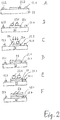
- Fig. 2 which comprises Figs. 2A to 2F showing schematic cross-sectional representations of a semiconductor die and a structure to be built up on a contact pad thereof. It should be mentioned that Fig. 2 relates to laser-assisted fabrication of a frontside electrical conductor on the second upper surface of the semiconductor die. The same procedure can be performed in addition or alternatively with the fabrication of a backside electrical conductor on the first lower surface of the semiconductor die.
- Fig. 2A shows a semiconductor die 22 comprising a first upper main face and a second lower main face opposite to the first upper main face, and side faces connecting the first and second main face with each other, and contact pads 22.2, 22.3, and 22.4 disposed on the first upper main face.
- the semiconductor die 22 can be an IGBT or MOSFET die and the contact pad 22.2 can be a source or emitter contact pad and the contact pads 22.3 and 22.4 can be, for example, a gate contact pad, a current sense contact pad, or a temperature sense contact pad, respectively. It should be mentioned that it is also possible to apply one or more additional metal layers onto the contact pads in order to increase the stress resistance of the contact pads against the laser assisted structuring process.
- Fig. 2B shows the semiconductor die 22 after applying a first amount of a metallic material 23.1 as, for example, copper onto an upper surface of the source contact pad 22.2.
- a metallic material 23.1 as, for example, copper onto an upper surface of the source contact pad 22.2.
- the metallic material can be applied in the form of portions like balls or blocks. However, also other methods of applying the metallic material can be used as will be shown and explained in connection with Fig. 3 .
- the metallic material can be applied directly onto the upper surface of the source contact pad 22.2 and/or the first contact pad without any solder layer or other intermediate layer.
- a barrier layer or a barrier layer stack including two or more barrier layers can be applied before building up the structure. This will be explained in some more detail below.
- Fig. 2C shows the semiconductor die 22 during irradiating the metallic material with an intense laser beam as indicated by the arrows.
- the laser source can, for example, be an infrared laser as, for example, a Nd:YAG laser emitting radiation in the infrared spectrum, in particular at a wavelength of 1064 nm.
- the laser irradiation heats up the metallic material 23.1 and makes it melt so that the portions of the metallic material 23.1 flow into each other and after cooling and solidifying will form a uniform and coherent block of metallic material.
- Fig. 2D shows the semiconductor die 22 after finishing the laser irradiation.
- the deposited metallic material 23.1 has turned into a uniform and coherent block 23 of metallic, in particular copper material.
- Fig. 2E shows the semiconductor die 22 after applying a second amount of a metallic material 23.2 onto an upper surface of the fabricated metallic material 23. After that a new laser irradiation for irradiating the second amount of metallic material 23.2 is carried out in the same way as was shown and explained in connection with Fig. 2C and is here not being shown again.
- Fig. 2F shows the semiconductor die 22 after finishing this new laser irradiation.
- the deposited metallic material 23.2 has also turned into a uniform and coherent block 23 of metallic, in particular copper material.
- the method 100 can be carried out in such a way that the metallic structure can be built up in such a way that its lateral dimensions increase whilst growing the structure.
- the present disclosure offers the possibility of an extension of the pitch of contact pads on the upper surface of the semiconductor die and/or the possibility of arranging further contact pads.
- the present disclosure allows for relaxing the design rules. Furthermore it provides more robustness against z-height-variation due to the compressibility and also some spring force effect of the metallic structure.
- the metallic material can be freely selected whilst copper is preferred. Aspect-ratio and fan-out-geometry can also be optional.
- the method of the present disclosure can further be used for a software defined manufacturing of metallic products and structures, also for products with small number of quantities.
- the method allows to fabricate metallic structures with rounded edges in contrast to other methods like, for example, punching which in general results in rather sharp edges. Rounded corners are very important for high-voltage applications as they can prevent high electrical fields in the vicinity of corners or edges.
- this method can be applied for semiconductor chips of any kind of semiconductor material.
- the method is, however, particularly interesting for wide bandgap semiconductor dies, like, for example, SiC semiconductor dies, or GaN semiconductor dies, in particular power semiconductor dies thereof as they are often very small so that also the contact pads are very small. In case of small contact pads it becomes very advantageous to build thick interconnect structures thereupon for dissipating the heat generated by the SiC or GaN power die.
- the method can also be further applied for multi die applications, i.e. for two or more semiconductor dies and in particular for fabricating electrical interconnects between the semiconductor dies.
- the method 100 further comprises applying the encapsulant such that an upper surface of the metallic structure is at least in part not covered by the encapsulant.
- an active cooling structure could be built into the upper surface of the metallic structure.
- a cooling channel could be formed into the upper surface, the cooling channel being connected with an inlet and outlet so that a cooling medium could be supplied to the cooling channel. All these measures and features can also be employed when forming a backside electrical interconnect.
- the semiconductor transistor die comprises one or more further contact pads on the second main face, wherein the method further comprises fabricating an electrical conductor also on one or more of the further contact pads by laser-assisted structuring of metallic structures. An example thereof will also be shown later.
- the method further comprises disposing a barrier layer or a barrier layer stack including two or more barrier layers onto the second contact pad and/or the first contact pad before fabricating the metallic structure.
- a barrier layer or a barrier layer stack including two or more barrier layers onto the second contact pad and/or the first contact pad before fabricating the metallic structure.
- Suitable thin layers could be for example Ti, TiN, Ta, TaN, TiW, W, or stacks of these materials.
- the semiconductor die comprises a contact pad on the first lower main surface and that a backside interconnect is fabricated on this contact pad.
- laser assisted structuring is applied with either one of the frontside or the backside interconnect or with both of them.
- the method further comprises providing a die carrier and disposing the semiconductor die onto the die carrier.
- the semiconductor die can, for example, be disposed onto the die carrier before fabricating the frontside electrical connector by laser-assisted structuring and/or after fabricating the backside electrical connector by laser-assisted structuring of a metallic structure.
- Fig. 3 shows an example of an apparatus for carrying out a method for fabricating a semiconductor die package according to the first aspect.
- the apparatus 30 as shown in Fig. 3 is based on supplying the metallic material in powder form.
- the apparatus 30 comprises a powder feed member 31 in which a larger quantity of metal powder is disposed on a platform which platform can be continuously moved upwards.
- a squeegee 32 conveys a portion of the powder towards a build platform 33 where it can be deposited onto the contact pad or a yet developed metallic structure with a given geometry.
- balls or blocks of the metallic material are thrown onto the surface of the contact pad or the die carrier and are then on-the-flight melted by the impinging laser beam.
- the apparatus 30 further comprises a laser source 34 and a mirror 35 or other kind of deflection unit for deflecting the laser beam onto at least a portion of the metal powder in the build platform 33.
- the mirror 35 can be rotatable to deflect the laser beam in any way and on any desired regions of the metallic powder.
- the apparatus 30 further comprises an overflow container 36 for collecting up unused metallic powder.
- Fig. 4 shows an example of a semiconductor die package according to the second aspect.
- the semiconductor die package 10 of Fig. 4 comprises a die carrier 11, a semiconductor transistor die 12 disposed on the die carrier 11, the semiconductor transistor die 12 comprising a first contact pad 12.1 on a first lower main face and a second contact pad 12.2 on an upper main face, an electrical conductor 13 disposed on the second contact pad 12.2 and fabricated by laser-assisted structuring of a metallic material, and an encapsulant 14 covering the die carrier 11, the semiconductor die 12, and at least a portion of the electrical conductor 13.
- the electrical conductor 13 is directly connected with the second contact pad 12.2 with no further layer in between.
- a barrier layer is disposed between second contact pad and the upper main face of the semiconductor die 12.
- the barrier layer comprises one of Ti, TiN, Ta, TaN, TiW, W, or any kind of stacks of these materials.
- the semiconductor die 11 is a SiC die.
- the semiconductor transistor die 11 is a power semiconductor transistor die, in particular a power IGBT die or a power MOSFET die, or a thyristor die.
- an upper surface of the metallic structure 13 is at least in part not covered by the encapsulant 14. This allows for efficient double-side cooling by applying a heatsink onto the upper surface of the metallic structure 13.
- the semiconductor die package 10 further comprises the semiconductor transistor die 12 comprising one or more further contact pads 12.3 on the second main face, and an electrical conductor 15 disposed on one or more of the further contact pads 12.3 and also fabricated by laser-assisted structuring of metallic structures.
- the electrical conductor 13 can be formed homogeneous or continuous or coherent such as shown in the example of Fig. 4 . That is, also a portion of the electrical conductor 13 extending beyond the package, i.e. beyond a side face of the encapsulant 14 can still be formed by the additive fabrication method. However, it can also be the case that only a first portion of the electrical conductor, namely a first portion adjacent the contact pad 12.2 is fabricated by the additive fabrication method, and further portions of the electrical conductor 13 are produced by other methods. This holds true as well for the electrical connector 15. A respective example will be shown and explained below.
- Fig. 5 shows a further example of a not yet packaged semiconductor device in which example a clip-like structure has been produced by the method according to the first aspect.
- the die carrier can be either one of a portion of a leadframe, a directed copper bond (DCB), an active metal braze (AMB), or an isolated metal substrate (IMS).
- DCB directed copper bond
- AMB active metal braze
- IMS isolated metal substrate
- the semiconductor die package 30 of Fig. 5 comprises a die carrier 31, a semiconductor transistor die 32 disposed on the die carrier 31, the semiconductor transistor die 32 comprising a first contact pad (not visible) on a first lower main face and a second contact pad (not visible) on an upper main face, an electrical conductor 33 disposed on the second contact pad and fabricated in part by laser-assisted structuring of a metallic material.
- the semiconductor die package After applying an encapsulant so that it covers the die carrier 31, the semiconductor die 32, and at least a portion of the electrical conductor 33, the result will be a semiconductor die package according to the second aspect.
- the semiconductor die package may be configured such that it contains single discrete semiconductor dies as well as modules containing two or more semiconductor dies like, for example, power modules and intelligent power modules.
- the encapsulant can then be an resin, in particular an epoxy resin, as well as a silicone material.
- the electrical conductor 33 is composed of three portions, namely a first portion 33.1 formed directly on the contact pad, a second portion 33.2 which is the clip-like structure, and a third portion 33.3 which may form an external contact. More specifically, the first portion 33.1 may have been formed by the additive fabrication method, and also the second portion 33.2, namely the clip-like structure, may have also been formed by the additive fabrication method, and the third portion 33.3, in particular the external connector 33.3, may be part of a leadframe. In particular also the die carrier 31 may be part of a leadframe, in particular of the same leadframe which the external contact 33.3 is a part of.
- Fig. 6 shows an example of a particular 3D structure produced by the method according to the first aspect.
- a specific feature of the 3D structure 40 shown therein is that it is comprised of a structure in a portion of which the metallic material does not fill the entire space above the contact pad of the semiconductor die, but only selective areas of the available space.
- the 3D structure shown comprises a lattice structure, i.e. any possible kind of an openwork framework consisting of a crisscrossed pattern of strips or bars of metallic material.
- the lattice structure is formed by crossing the strips or bars to form a grid or weave.
- the 3D structure 40 shown in Fig. 6 comprises a first contiguous portion 41 onto which is applied a lattice portion 42 which is again followed by a further contiguous portion 43.
- Example 1 is a method for fabricating a semiconductor die package, the method comprising providing a semiconductor transistor die, the semiconductor transistor die comprising possibly a first contact pad on a first lower main face and a second contact pad on an upper main face, fabricating a frontside electrical conductor onto the second contact pad and possibly also a backside electrical conductor onto the first contact pad, and applying an encapsulant covering the semiconductor die, and at least a portion of the frontside electrical conductor, wherein the frontside electrical conductor and/or the backside electrical conductor is fabricated by laser-assisted structuring of a metallic structure.
- Example 2 the subject matter of Example 1 can optionally further include that fabricating the frontside electrical conductor and/or the backside electrical conductor comprises
- Example 3 the subject matter of Example 1 or 2 can optionally further comprises repeating steps i. and ii. by applying further metallic material onto the fabricated metallic structure and irradiating at least a portion of the further metallic material with the laser beam.
- Example 4 the subject matter of any one of the preceding Examples can optionally further include that the metallic material is deposited in the form of a metallic powder or metallic balls or blocks.
- Example 5 the subject matter of any one of the preceding Examples can optionally further include that before fabricating the electrical conductor no layer, in particular no solder layer, is deposited onto the second contact pad and/or the first contact pad.
- Example 6 the subject matter of any one of the preceding Examples can optionally further include that the semiconductor die is one or more of a wide bandgap semiconductor die, a SiC die, or a GaN die.
- the semiconductor die is one or more of a wide bandgap semiconductor die, a SiC die, or a GaN die.
- Example 7 the subject matter of any one of the preceding Examples can optionally further include that the semiconductor transistor die is a power semiconductor transistor die, in particular a power IGBT die or a power MOSFET die, or a thyristor die.
- the semiconductor transistor die is a power semiconductor transistor die, in particular a power IGBT die or a power MOSFET die, or a thyristor die.
- Example 8 the subject matter of any one of the preceding Examples can optionally further comprises applying the encapsulant such that an upper surface of the metallic structure is at least in part not covered by the encapsulant.
- Example 9 the subject matter of any one of the preceding Examples can optionally further include that the semiconductor transistor die comprises one or more further contact pads on the second main face, wherein the method further comprises fabricating an electrical conductor also on one or more of the further contact pads by laser-assisted structuring of metallic structures.
- Example 10 the subject matter of any one of the preceding Examples can optionally further comprise disposing a barrier layer or a barrier layer stack including two or more barrier layers onto the second contact pad and/or the first contact pad before fabricating the metallic structure.
- Example 11 the subject matter of any one of the preceding Examples can optionally further comprise providing a die carrier and disposing the semiconductor die onto the die carrier.
- Example 12 is a semiconductor die package, comprising a semiconductor transistor die, the semiconductor transistor die comprising possibly a first contact pad on a first lower main face and/or a second contact pad on an upper main face, an electrical conductor disposed on the second contact pad and fabricated by laser-assisted structuring of a metallic material, and an encapsulant covering the semiconductor die, and at least a portion of the electrical conductor.
- Example 13 the subject matter of Example 12 can optionally further comprise a die carrier, wherein the semiconductor die is disposed on the die carrier.
- Example 14 the subject matter of any one of the Examples 12 or 13 can optionally further include that the electrical conductor is directly connected with the second contact pad with no further layer in between.
- Example 15 the subject matter of any one of the Examples 12 to 14 can optionally further include that the semiconductor die is one or more of a wide bandgap semiconductor die, a SiC die, or a GaN die.
- the semiconductor die is one or more of a wide bandgap semiconductor die, a SiC die, or a GaN die.
- Example 16 the subject matter of any one of the Examples 12 to 15 can optionally further include that the semiconductor transistor die (11; 31) is a power semiconductor transistor die, in particular a power IGBT die or a power MOSFET die, or a thyristor die.
- the semiconductor transistor die (11; 31) is a power semiconductor transistor die, in particular a power IGBT die or a power MOSFET die, or a thyristor die.
- Example 17 the subject matter of any one of the Examples 12 to 16 can optionally further include that an upper surface of the electrical conductor is at least in part not covered by the encapsulant.
- Example 18 the subject matter of any one of the Examples 12 to 17 can optionally further comprise the semiconductor transistor die comprising one or more further contact pads on the second main face, and an electrical conductor on one or more of the further contact pads fabricated by laser-assisted structuring of metallic structures.
Landscapes
- Engineering & Computer Science (AREA)
- Chemical & Material Sciences (AREA)
- Materials Engineering (AREA)
- Manufacturing & Machinery (AREA)
- Mechanical Engineering (AREA)
- Physics & Mathematics (AREA)
- Optics & Photonics (AREA)
- Composite Materials (AREA)
- Internal Circuitry In Semiconductor Integrated Circuit Devices (AREA)
- Structures Or Materials For Encapsulating Or Coating Semiconductor Devices Or Solid State Devices (AREA)
Abstract
A method for fabricating a semiconductor die package, the method comprises providing a semiconductor transistor die (12), the semiconductor transistor die (12) comprising possibly a first contact pad (12.1) on a first lower main face and/or a second contact pad (12.2) on an upper main face, fabricating a frontside electrical conductor (13) onto the second contact pad (12.2) and possibly a backside electrical conductor onto the first contact pad (12.1), and applying an encapsulant (14) covering the semiconductor die, and at least a portion of the electrical conductor (13), wherein the frontside electrical conductor (13) and/or the backside electrical conductor is fabricated by laser-assisted structuring of a metallic structure..
Description
- The present disclosure is related to a method for fabricating a semiconductor die package and to a semiconductor die package.
- In the field of semiconductor power device fabrication an increasing problem is the efficient dissipation of the heat produced by the power device. This problem is further exacerbated by the increasing miniaturization and density of semiconductor power devices. Wide bandgap semiconductor like, for example, SiC or GaN devices within TO packages do have an effective bottom-side cooling, especially for thick leadframe thicknesses. Nevertheless it has been found out during (reliability) short-circuit tests, that the surface temperature exceeds the melting point of the layer stack, and mold compound degradation may occur due to overheating since the heat dissipation is not efficient enough. A double-side cooling (top and bottom side) can solve this problem. While bottom side cooling is state of the art, the topside cooling underlies some challenges, which are generated by design-rule limitations, for instance up to 1000 pm edge termination due to electro fields. If additionally a 500 µm clearance around the source pad is required for clip soldering, the remaining source pad area for cooling becomes very small for small (shrinked) chip sizes and/or suitable clips become a quite expensive solution for interconnect of the source/emitter and thermomechanical stress comes to a limit.
- A further problem of the increasing miniaturization of semiconductor power devices, in particular wide band gap semiconductor power devices like, for example, SiC or GaN power devices, is to conduct high amounts of electric current out of the power devices. A small source pad area is thus not only a problem of insufficient heat dissipation but also a problem of a too low electric current as the frontside interconnect cannot handle a high current output. In addition to that, wide bandgap semiconductors are known to be capable to provide rather fast switching speeds of, for example, > 100 kHz. In case of high switching speeds it is important to provide electrical conductors of low inductances. Therefore it is desirable to fabricate a frontside and backside interconnect of a low inductance.
- A first aspect of the present disclosure is related to a method for fabricating a semiconductor die package, the method comprising providing a semiconductor transistor die, the semiconductor transistor die comprising a first contact pad on a first lower main face and possibly a second contact pad on an upper main face, fabricating a frontside electrical conductor onto the second contact pad and possibly a backside electrical conductor onto the first contact pad, and applying an encapsulant covering the semiconductor die, and at least a portion of the frontside electrical conductor, wherein the frontside electrical conductor and/or the backside electrical conductor is fabricated by laser-assisted structuring of a metallic structure.
- A second aspect of the present disclosure is related to a semiconductor die package, comprising a semiconductor transistor die comprising possibly a first contact pad on a first lower main face and/or a second contact pad on an upper main face, an electrical conductor disposed on the second contact pad and fabricated by laser-assisted structuring of a metallic material, and an encapsulant covering the semiconductor die, and at least a portion of the electrical conductor.
- The accompanying drawings are included to provide a further understanding of embodiments and are incorporated in and constitute a part of this specification. The drawings illustrate embodiments and together with the description serve to explain principles of embodiments. Other embodiments and many of the intended advantages of the embodiments will be readily appreciated as they become better understood by reference to the following detailed description.
- The elements of the drawings are not necessarily to scale relative to each other. Like reference numerals designate corresponding similar parts.
-
Fig. 1 shows a flow diagram for illustrating a method for fabricating a semiconductor die package according to the first aspect. -
Fig. 2 comprisesFigs. 2A to 2F and illustrates an example of a method for fabricating a semiconductor die package according to the first aspect. -
Fig. 3 shows an example of an apparatus for carrying out a method for fabricating a semiconductor die package according to the first aspect. -
Fig. 4 shows an example of a semiconductor die package according to the second aspect. -
Fig. 5 shows a further example of a semiconductor die package according to the second aspect in which example a clip-like structure has been produced by the method according to the first aspect. -
Fig. 6 shows an example of a 3D structure produced by the method according to the first aspect. - In the following detailed description, reference is made to the accompanying drawings, which form a part hereof, and in which is shown by way of illustration specific embodiments in which the disclosure may be practiced. In this regard, directional terminology, such as "top", "bottom", "front", "back", "leading", "trailing", etc., is used with reference to the orientation of the Figure(s) being described. Because components of embodiments can be positioned in a number of different orientations, the directional terminology is used for purposes of illustration and is in no way limiting. It is to be understood that other embodiments may be utilized and structural or logical changes may be made without departing from the scope of the present disclosure. The following detailed description, therefore, is not to be taken in a limiting sense, and the scope of the present disclosure is defined by the appended claims.
- It is to be understood that the features of the various exemplary embodiments described herein may be combined with each other, unless specifically noted otherwise.
- As employed in this specification, the terms "bonded", "attached", "connected", "coupled" and/or "electrically connected/electrically coupled" are not meant to mean that the elements or layers must directly be contacted together; intervening elements or layers may be provided between the "bonded", "attached", "connected", "coupled" and/or "electrically connected/electrically coupled" elements, respectively. However, in accordance with the disclosure, the above-mentioned terms may, optionally, also have the specific meaning that the elements or layers are directly contacted together, i.e. that no intervening elements or layers are provided between the "bonded", "attached", "connected", "coupled" and/or "electrically connected/electrically coupled" elements, respectively.
- Further, the word "over" used with regard to a part, element or material layer formed or located "over" a surface may be used herein to mean that the part, element or material layer be located (e.g. placed, formed, deposited, etc.) "indirectly on" the implied surface with one or more additional parts, elements or layers being arranged between the implied surface and the part, element or material layer. However, the word "over" used with regard to a part, element or material layer formed or located "over" a surface may, optionally, also have the specific meaning that the part, element or material layer be located (e.g. placed, formed, deposited, etc.) "directly on", e.g. in direct contact with, the implied surface.
-
Fig. 1 shows a flow diagram for illustrating a method for fabricating a semiconductor die package according to the first aspect. - According to
Fig. 1 , themethod 100 for fabricating a semiconductor die package comprises providing a semiconductor transistor die, the semiconductor transistor die comprising possibly a first contact pad on a first lower main face and/or a second contact pad on an upper main face (110), fabricating a frontside electrical conductor onto the second contact pad and possibly also a backside electrical conductor onto the first contact pad (120), and applying an encapsulant covering the semiconductor die, and at least a portion of the frontside electrical conductor (130). - According to an example of the
method 100 ofFig. 1 , fabricating the frontside electrical conductor and/or the backside electrical conductor comprises - i. Depositing a metallic material onto the second contact pad and/or the first contact pad, and
- ii. Irradiating at least a portion of the metallic material with a laser beam.
- According to a further example thereof, the method further comprises repeating steps i. and ii. by applying further metallic material onto the fabricated metallic structure and irradiating at least a portion of the further metallic material with the laser beam. Thereafter the steps i. and ii. can be repeated as many times as is required in order to obtain a desired structure of the electrical connector. The method can therefore be called an additive manufacturing method.
- According to a further example thereof, the method further comprises a post-process of conditioning the metallic material after laser-assisted structuring. Such post-process may include, for example, a heat treatment for annealing the metallic material so that crystal defects can be healed and crystal grain sizes of the metallic material can be optimized. Also possible voids or defects in the metallic material can be controlled, in particular the number of voids or defects can be reduced.
- The latter can at best be explained by means of
Fig. 2 which comprisesFigs. 2A to 2F showing schematic cross-sectional representations of a semiconductor die and a structure to be built up on a contact pad thereof. It should be mentioned thatFig. 2 relates to laser-assisted fabrication of a frontside electrical conductor on the second upper surface of the semiconductor die. The same procedure can be performed in addition or alternatively with the fabrication of a backside electrical conductor on the first lower surface of the semiconductor die. -
Fig. 2A shows asemiconductor die 22 comprising a first upper main face and a second lower main face opposite to the first upper main face, and side faces connecting the first and second main face with each other, and contact pads 22.2, 22.3, and 22.4 disposed on the first upper main face. The semiconductor die 22 can be an IGBT or MOSFET die and the contact pad 22.2 can be a source or emitter contact pad and the contact pads 22.3 and 22.4 can be, for example, a gate contact pad, a current sense contact pad, or a temperature sense contact pad, respectively. It should be mentioned that it is also possible to apply one or more additional metal layers onto the contact pads in order to increase the stress resistance of the contact pads against the laser assisted structuring process. -
Fig. 2B shows the semiconductor die 22 after applying a first amount of a metallic material 23.1 as, for example, copper onto an upper surface of the source contact pad 22.2. As shown inFig. 2B , the metallic material can be applied in the form of portions like balls or blocks. However, also other methods of applying the metallic material can be used as will be shown and explained in connection withFig. 3 . - Anyway the metallic material can be applied directly onto the upper surface of the source contact pad 22.2 and/or the first contact pad without any solder layer or other intermediate layer. As an exception thereof, in special cases a barrier layer or a barrier layer stack including two or more barrier layers can be applied before building up the structure. This will be explained in some more detail below.
-
Fig. 2C shows the semiconductor die 22 during irradiating the metallic material with an intense laser beam as indicated by the arrows. The laser source can, for example, be an infrared laser as, for example, a Nd:YAG laser emitting radiation in the infrared spectrum, in particular at a wavelength of 1064 nm. The laser irradiation heats up the metallic material 23.1 and makes it melt so that the portions of the metallic material 23.1 flow into each other and after cooling and solidifying will form a uniform and coherent block of metallic material. -
Fig. 2D shows the semiconductor die 22 after finishing the laser irradiation. As a result the deposited metallic material 23.1 has turned into a uniform andcoherent block 23 of metallic, in particular copper material. -
Fig. 2E shows the semiconductor die 22 after applying a second amount of a metallic material 23.2 onto an upper surface of the fabricatedmetallic material 23. After that a new laser irradiation for irradiating the second amount of metallic material 23.2 is carried out in the same way as was shown and explained in connection withFig. 2C and is here not being shown again. -
Fig. 2F shows the semiconductor die 22 after finishing this new laser irradiation. As a result the deposited metallic material 23.2 has also turned into a uniform andcoherent block 23 of metallic, in particular copper material. - In such a way, that is by successively repeating the steps of applying metallic material and thereafter irradiating it with the laser beam, a more or less complex 3D structure can be built up onto the contact pads.
- According to an example of the method as shown in
Figs. 1 or2 , themethod 100 can be carried out in such a way that the metallic structure can be built up in such a way that its lateral dimensions increase whilst growing the structure. In particular, it is possible to increase the lateral dimensions in each step of applying a further amount of metallic material onto the structure. In this way it is possible to build up a massive 3D structure for an improved heat dissipation in combination with low inductance even when starting from a rather small-sized contact pad. - As further advantages, the present disclosure offers the possibility of an extension of the pitch of contact pads on the upper surface of the semiconductor die and/or the possibility of arranging further contact pads. In general, the present disclosure allows for relaxing the design rules. Furthermore it provides more robustness against z-height-variation due to the compressibility and also some spring force effect of the metallic structure. The metallic material can be freely selected whilst copper is preferred. Aspect-ratio and fan-out-geometry can also be optional. The method of the present disclosure can further be used for a software defined manufacturing of metallic products and structures, also for products with small number of quantities. As a further advantage of the present disclosure, the method allows to fabricate metallic structures with rounded edges in contrast to other methods like, for example, punching which in general results in rather sharp edges. Rounded corners are very important for high-voltage applications as they can prevent high electrical fields in the vicinity of corners or edges.
- It should be noted further that this method can be applied for semiconductor chips of any kind of semiconductor material. The method is, however, particularly interesting for wide bandgap semiconductor dies, like, for example, SiC semiconductor dies, or GaN semiconductor dies, in particular power semiconductor dies thereof as they are often very small so that also the contact pads are very small. In case of small contact pads it becomes very advantageous to build thick interconnect structures thereupon for dissipating the heat generated by the SiC or GaN power die. The method can also be further applied for multi die applications, i.e. for two or more semiconductor dies and in particular for fabricating electrical interconnects between the semiconductor dies.
- According to an example of the method as shown in
Figs. 1 or2 , themethod 100 further comprises applying the encapsulant such that an upper surface of the metallic structure is at least in part not covered by the encapsulant. This can be very advantageous as in such a case a further heatsink can be applied on top of the exposed metallic structure allowing an efficient double-side cooling. Alternatively or in addition to that, an active cooling structure could be built into the upper surface of the metallic structure. For example, a cooling channel could be formed into the upper surface, the cooling channel being connected with an inlet and outlet so that a cooling medium could be supplied to the cooling channel. All these measures and features can also be employed when forming a backside electrical interconnect. - According to an example of the method as shown in
Figs. 1 or2 , the semiconductor transistor die comprises one or more further contact pads on the second main face, wherein the method further comprises fabricating an electrical conductor also on one or more of the further contact pads by laser-assisted structuring of metallic structures. An example thereof will also be shown later. - According to an example of the method as shown in
Figs. 1 or2 , the method further comprises disposing a barrier layer or a barrier layer stack including two or more barrier layers onto the second contact pad and/or the first contact pad before fabricating the metallic structure. Dependent on the chosen metallization it can be necessary or desirable to implement such a barrier layer between the metallization material and the upper surface of the semiconductor die. Suitable thin layers could be for example Ti, TiN, Ta, TaN, TiW, W, or stacks of these materials. - According to an example of the method of the first aspect, it is also possible that the semiconductor die comprises a contact pad on the first lower main surface and that a backside interconnect is fabricated on this contact pad. In such a case it can be that laser assisted structuring is applied with either one of the frontside or the backside interconnect or with both of them.
- According to an example of the method of the first aspect, the method further comprises providing a die carrier and disposing the semiconductor die onto the die carrier. The semiconductor die can, for example, be disposed onto the die carrier before fabricating the frontside electrical connector by laser-assisted structuring and/or after fabricating the backside electrical connector by laser-assisted structuring of a metallic structure.
-
Fig. 3 shows an example of an apparatus for carrying out a method for fabricating a semiconductor die package according to the first aspect. - The
apparatus 30 as shown inFig. 3 is based on supplying the metallic material in powder form. In particular, theapparatus 30 comprises apowder feed member 31 in which a larger quantity of metal powder is disposed on a platform which platform can be continuously moved upwards. Above the platform asqueegee 32 conveys a portion of the powder towards abuild platform 33 where it can be deposited onto the contact pad or a yet developed metallic structure with a given geometry. - It can also be that balls or blocks of the metallic material are thrown onto the surface of the contact pad or the die carrier and are then on-the-flight melted by the impinging laser beam.
- The
apparatus 30 further comprises alaser source 34 and amirror 35 or other kind of deflection unit for deflecting the laser beam onto at least a portion of the metal powder in thebuild platform 33. Themirror 35 can be rotatable to deflect the laser beam in any way and on any desired regions of the metallic powder. Theapparatus 30 further comprises anoverflow container 36 for collecting up unused metallic powder. -
Fig. 4 shows an example of a semiconductor die package according to the second aspect. - The semiconductor die
package 10 ofFig. 4 comprises adie carrier 11, a semiconductor transistor die 12 disposed on thedie carrier 11, the semiconductor transistor die 12 comprising a first contact pad 12.1 on a first lower main face and a second contact pad 12.2 on an upper main face, anelectrical conductor 13 disposed on the second contact pad 12.2 and fabricated by laser-assisted structuring of a metallic material, and anencapsulant 14 covering thedie carrier 11, the semiconductor die 12, and at least a portion of theelectrical conductor 13. - According to an example of the
semiconductor die package 10 ofFig. 4 , theelectrical conductor 13 is directly connected with the second contact pad 12.2 with no further layer in between. - According to another example of the semiconductor die package of
Fig. 4 , a barrier layer is disposed between second contact pad and the upper main face of the semiconductor die 12. According to a further example thereof, the barrier layer comprises one of Ti, TiN, Ta, TaN, TiW, W, or any kind of stacks of these materials. - According to an example of the semiconductor die package of
Fig. 4 , the semiconductor die 11 is a SiC die. - According to an example of the semiconductor die package of
Fig. 4 , the semiconductor transistor die 11 is a power semiconductor transistor die, in particular a power IGBT die or a power MOSFET die, or a thyristor die. - According to another example of the semiconductor die package of
Fig. 4 , an upper surface of themetallic structure 13 is at least in part not covered by theencapsulant 14. This allows for efficient double-side cooling by applying a heatsink onto the upper surface of themetallic structure 13. - According to another example of the semiconductor die package of
Fig. 4 , thesemiconductor die package 10 further comprises the semiconductor transistor die 12 comprising one or more further contact pads 12.3 on the second main face, and anelectrical conductor 15 disposed on one or more of the further contact pads 12.3 and also fabricated by laser-assisted structuring of metallic structures. - According to an example of the semiconductor die package of
Fig. 4 , theelectrical conductor 13 can be formed homogeneous or continuous or coherent such as shown in the example ofFig. 4 . That is, also a portion of theelectrical conductor 13 extending beyond the package, i.e. beyond a side face of theencapsulant 14 can still be formed by the additive fabrication method. However, it can also be the case that only a first portion of the electrical conductor, namely a first portion adjacent the contact pad 12.2 is fabricated by the additive fabrication method, and further portions of theelectrical conductor 13 are produced by other methods. This holds true as well for theelectrical connector 15. A respective example will be shown and explained below. -
Fig. 5 shows a further example of a not yet packaged semiconductor device in which example a clip-like structure has been produced by the method according to the first aspect. - The die carrier can be either one of a portion of a leadframe, a directed copper bond (DCB), an active metal braze (AMB), or an isolated metal substrate (IMS).
- The semiconductor die
package 30 ofFig. 5 comprises adie carrier 31, a semiconductor transistor die 32 disposed on thedie carrier 31, the semiconductor transistor die 32 comprising a first contact pad (not visible) on a first lower main face and a second contact pad (not visible) on an upper main face, anelectrical conductor 33 disposed on the second contact pad and fabricated in part by laser-assisted structuring of a metallic material. - After applying an encapsulant so that it covers the
die carrier 31, the semiconductor die 32, and at least a portion of theelectrical conductor 33, the result will be a semiconductor die package according to the second aspect. It should be noted that the semiconductor die package may be configured such that it contains single discrete semiconductor dies as well as modules containing two or more semiconductor dies like, for example, power modules and intelligent power modules. The encapsulant can then be an resin, in particular an epoxy resin, as well as a silicone material. - The
electrical conductor 33 is composed of three portions, namely a first portion 33.1 formed directly on the contact pad, a second portion 33.2 which is the clip-like structure, and a third portion 33.3 which may form an external contact. More specifically, the first portion 33.1 may have been formed by the additive fabrication method, and also the second portion 33.2, namely the clip-like structure, may have also been formed by the additive fabrication method, and the third portion 33.3, in particular the external connector 33.3, may be part of a leadframe. In particular also thedie carrier 31 may be part of a leadframe, in particular of the same leadframe which the external contact 33.3 is a part of. - The previous examples as shown in
Figs. 4 and5 presented devices in which the additive fabrication method is used to fabricate metallic structures that are homogeneous and coherent in themselves. In the following it will be shown that also other types of structures can be produced with the additive fabrication method. -
Fig. 6 shows an example of a particular 3D structure produced by the method according to the first aspect. A specific feature of the 3D structure 40 shown therein is that it is comprised of a structure in a portion of which the metallic material does not fill the entire space above the contact pad of the semiconductor die, but only selective areas of the available space. More specifically, the 3D structure shown comprises a lattice structure, i.e. any possible kind of an openwork framework consisting of a crisscrossed pattern of strips or bars of metallic material. The lattice structure is formed by crossing the strips or bars to form a grid or weave. More specifically, the 3D structure 40 shown inFig. 6 comprises a firstcontiguous portion 41 onto which is applied alattice portion 42 which is again followed by a furthercontiguous portion 43. - The use of such structures as shown in
Fig. 6 can in particular be advantageous when a massive heatsink is intended to be disposed on an upper surface of the metallic structure. If in such a case a homogeneous or continuous metallic structure of the electrical connector is used such is shown inFig. 4 or5 , then plastic strain may be induced by the heatsink. Plastic strain can be observed by the presence of dislocations or displacements of part of the crystal lattice. Such strain effects can result in unwanted cracking of the material, as is the case with residual plastic strain. All this can be avoided when using a lattice structure of the electrical connector which lattice structure can deform itself without any structural alterations of the metallic material itself taken place. - Example 1 is a method for fabricating a semiconductor die package, the method comprising providing a semiconductor transistor die, the semiconductor transistor die comprising possibly a first contact pad on a first lower main face and a second contact pad on an upper main face, fabricating a frontside electrical conductor onto the second contact pad and possibly also a backside electrical conductor onto the first contact pad, and applying an encapsulant covering the semiconductor die, and at least a portion of the frontside electrical conductor, wherein the frontside electrical conductor and/or the backside electrical conductor is fabricated by laser-assisted structuring of a metallic structure.
- In Example 2, the subject matter of Example 1 can optionally further include that fabricating the frontside electrical conductor and/or the backside electrical conductor comprises
- i. Depositing a metallic material onto the second contact pad and/or the first contact pad, and
- ii. Irradiating at least a portion of the metallic material with a laser beam.
- In Example 3, the subject matter of Example 1 or 2 can optionally further comprises repeating steps i. and ii. by applying further metallic material onto the fabricated metallic structure and irradiating at least a portion of the further metallic material with the laser beam.
- In Example 4, the subject matter of any one of the preceding Examples can optionally further include that the metallic material is deposited in the form of a metallic powder or metallic balls or blocks.
- In Example 5, the subject matter of any one of the preceding Examples can optionally further include that before fabricating the electrical conductor no layer, in particular no solder layer, is deposited onto the second contact pad and/or the first contact pad.
- In Example 6, the subject matter of any one of the preceding Examples can optionally further include that the semiconductor die is one or more of a wide bandgap semiconductor die, a SiC die, or a GaN die.
- In Example 7, the subject matter of any one of the preceding Examples can optionally further include that the semiconductor transistor die is a power semiconductor transistor die, in particular a power IGBT die or a power MOSFET die, or a thyristor die.
- In Example 8, the subject matter of any one of the preceding Examples can optionally further comprises applying the encapsulant such that an upper surface of the metallic structure is at least in part not covered by the encapsulant.
- In Example 9, the subject matter of any one of the preceding Examples can optionally further include that the semiconductor transistor die comprises one or more further contact pads on the second main face, wherein the method further comprises fabricating an electrical conductor also on one or more of the further contact pads by laser-assisted structuring of metallic structures.
- In Example 10, the subject matter of any one of the preceding Examples can optionally further comprise disposing a barrier layer or a barrier layer stack including two or more barrier layers onto the second contact pad and/or the first contact pad before fabricating the metallic structure.
- In Example 11, the subject matter of any one of the preceding Examples can optionally further comprise providing a die carrier and disposing the semiconductor die onto the die carrier.
- Example 12 is a semiconductor die package, comprising a semiconductor transistor die, the semiconductor transistor die comprising possibly a first contact pad on a first lower main face and/or a second contact pad on an upper main face, an electrical conductor disposed on the second contact pad and fabricated by laser-assisted structuring of a metallic material, and an encapsulant covering the semiconductor die, and at least a portion of the electrical conductor.
- In Example 13, the subject matter of Example 12 can optionally further comprise a die carrier, wherein the semiconductor die is disposed on the die carrier.
- In Example 14, the subject matter of any one of the Examples 12 or 13 can optionally further include that the electrical conductor is directly connected with the second contact pad with no further layer in between.
- In Example 15, the subject matter of any one of the Examples 12 to 14 can optionally further include that the semiconductor die is one or more of a wide bandgap semiconductor die, a SiC die, or a GaN die.
- In Example 16, the subject matter of any one of the Examples 12 to 15 can optionally further include that the semiconductor transistor die (11; 31) is a power semiconductor transistor die, in particular a power IGBT die or a power MOSFET die, or a thyristor die.
- In Example 17, the subject matter of any one of the Examples 12 to 16 can optionally further include that an upper surface of the electrical conductor is at least in part not covered by the encapsulant.
- In Example 18, the subject matter of any one of the Examples 12 to 17 can optionally further comprise the semiconductor transistor die comprising one or more further contact pads on the second main face, and an electrical conductor on one or more of the further contact pads fabricated by laser-assisted structuring of metallic structures.
- In addition, while a particular feature or aspect of an embodiment of the disclosure may have been disclosed with respect to only one of several implementations, such feature or aspect may be combined with one or more other features or aspects of the other implementations as may be desired and advantageous for any given or particular application. Furthermore, to the extent that the terms "include", "have", "with", or other variants thereof are used in either the detailed description or the claims, such terms are intended to be inclusive in a manner similar to the term "comprise". Furthermore, it should be understood that embodiments of the disclosure may be implemented in discrete circuits, partially integrated circuits or fully integrated circuits or programming means. Also, the term "exemplary" is merely meant as an example, rather than the best or optimal. It is also to be appreciated that features and/or elements depicted herein are illustrated with particular dimensions relative to one another for purposes of simplicity and ease of understanding, and that actual dimensions may differ substantially from that illustrated herein.
- Although specific embodiments have been illustrated and described herein, it will be appreciated by those of ordinary skill in the art that a variety of alternate and/or equivalent implementations may be substituted for the specific embodiments shown and described without departing from the scope of the present disclosure. This application is intended to cover any adaptations or variations of the specific embodiments discussed herein. Therefore, it is intended that this disclosure be limited only by the claims and the equivalents thereof.
Claims (18)
- A method (100) for fabricating a semiconductor die package, the method comprising- providing a semiconductor transistor die, the semiconductor transistor die comprising possibly a first contact pad on a first lower main face and a second contact pad on an upper main face (110);- fabricating a frontside electrical conductor onto the second contact pad and possibly also a backside electrical conductor onto the first contact pad (120); and- applying an encapsulant covering the semiconductor die, and at least a portion of the frontside electrical conductor (130), wherein- the frontside electrical conductor and/or the backside electrical conductor is fabricated by laser-assisted structuring of a metallic structure.
- The method (100) according to claim 1, wherein fabricating the frontside electrical conductor and/or the backside electrical conductor comprisesi. Depositing a metallic material onto the second contact pad and/or the first contact pad, andii. Irradiating at least a portion of the metallic material with a laser beam.
- The method (100) according to claim 2, further comprising
repeating steps i. and ii. by applying further metallic material onto the fabricated metallic structure and irradiating at least a portion of the further metallic material with the laser beam. - The method (100) according to claim 2 or 3, wherein
the metallic material is deposited in the form of a metallic powder or metallic balls or blocks. - The method (100) according to any one of the preceding claims, wherein
before fabricating the electrical conductor no layer, in particular no solder layer, is deposited onto the second contact pad and/or the first contact pad. - The method (100) according to any one of the preceding claims, wherein
the semiconductor die is one or more of a wide bandgap semiconductor die, a SiC die, or a GaN die. - The method (100) according to any one of the preceding claims, wherein
the semiconductor transistor die is a power semiconductor transistor die, in particular a power IGBT die or a power MOSFET die, or a thyristor die. - The method (100) according to any one of the preceding claims, further comprising
applying the encapsulant such that an upper surface of the metallic structure is at least in part not covered by the encapsulant. - The method (100) according to any one of the preceding claims, wherein
the semiconductor transistor die comprises one or more further contact pads on the second main face, wherein the method further comprises fabricating an electrical conductor also on one or more of the further contact pads by laser-assisted structuring of metallic structures. - The method (100) according to any one of the preceding claims, further comprising
disposing a barrier layer or a barrier layer stack including two or more barrier layers onto the second contact pad and/or the first contact pad before fabricating the metallic structure. - The method according to any one of the preceding claims, further comprising
providing a die carrier and disposing the semiconductor die onto the die carrier. - A semiconductor die package (10; 30), comprising- a semiconductor transistor die (12; 32), the semiconductor transistor die (12; 32) comprising possibly a first contact pad (12.1) on a first lower main face and/or a second contact pad (12.2) on an upper main face;- an electrical conductor (13; 33.1) disposed on the second contact pad (12.2) and fabricated by laser-assisted structuring of a metallic material; and- an encapsulant (14) covering the semiconductor die (12; 32), and at least a portion of the electrical conductor (13; 33.1).
- The semiconductor die package (10; 30) according to claim 12, further comprising
a die carrier (11; 31), wherein the semiconductor die (12; 32) is disposed on the die carrier (11; 31). - The semiconductor die package (10; 30) according to claim 12 or 13, wherein
the electrical conductor (13, 33.1) is directly connected with the second contact pad (12.2) with no further layer in between. - The semiconductor die package (10; 30) according to any one of claims 12 to 14, wherein
the semiconductor die (11; 31) is one or more of a wide bandgap semiconductor die, a SiC die, or a GaN die. - The semiconductor die package (10; 30) according to any one of claims 12 to 15, wherein
the semiconductor transistor die (11; 31) is a power semiconductor transistor die, in particular a power IGBT die or a power MOSFET die, or a thyristor die. - The semiconductor die package (10; 30) according to any one of claims 12 to 16, wherein
an upper surface of the electrical conductor (13) is at least in part not covered by the encapsulant (14). - The semiconductor die package (10) according to any one of claims 12 to 17, further comprising
the semiconductor transistor die (12) comprising one or more further contact pads (12.3) on the second main face, and
an electrical conductor (15) on one or more of the further contact pads (12.3) fabricated by laser-assisted structuring of metallic structures.
Priority Applications (4)
| Application Number | Priority Date | Filing Date | Title |
|---|---|---|---|
| EP20152722.3A EP3852132A1 (en) | 2020-01-20 | 2020-01-20 | Additive manufacturing of a frontside or backside interconnect of a semiconductor die |
| US17/149,891 US11688713B2 (en) | 2020-01-20 | 2021-01-15 | Additive manufacturing of a frontside or backside interconnect of a semiconductor die |
| CN202110067783.5A CN113140504B (en) | 2020-01-20 | 2021-01-19 | Additive manufacturing of front-side or back-side interconnects of semiconductor dies |
| US18/132,629 US12604752B2 (en) | 2020-01-20 | 2023-04-10 | Semiconductor die package |
Applications Claiming Priority (1)
| Application Number | Priority Date | Filing Date | Title |
|---|---|---|---|
| EP20152722.3A EP3852132A1 (en) | 2020-01-20 | 2020-01-20 | Additive manufacturing of a frontside or backside interconnect of a semiconductor die |
Publications (1)
| Publication Number | Publication Date |
|---|---|
| EP3852132A1 true EP3852132A1 (en) | 2021-07-21 |
Family
ID=69187551
Family Applications (1)
| Application Number | Title | Priority Date | Filing Date |
|---|---|---|---|
| EP20152722.3A Pending EP3852132A1 (en) | 2020-01-20 | 2020-01-20 | Additive manufacturing of a frontside or backside interconnect of a semiconductor die |
Country Status (3)
| Country | Link |
|---|---|
| US (2) | US11688713B2 (en) |
| EP (1) | EP3852132A1 (en) |
| CN (1) | CN113140504B (en) |
Cited By (1)
| Publication number | Priority date | Publication date | Assignee | Title |
|---|---|---|---|---|
| EP4439658A1 (en) * | 2023-03-29 | 2024-10-02 | Nexperia B.V. | A method for manufacturing a semiconductor package assembly as well as a semiconductor package assembly obtained with this method |
Families Citing this family (2)
| Publication number | Priority date | Publication date | Assignee | Title |
|---|---|---|---|---|
| CN114743947B (en) * | 2022-04-11 | 2023-09-19 | 中国工程物理研究院电子工程研究所 | Power device packaging structure and packaging method based on TO form |
| IT202200024687A1 (en) * | 2022-11-30 | 2024-05-30 | St Microelectronics Int Nv | Process for producing semiconductor devices and corresponding semiconductor device |
Citations (4)
| Publication number | Priority date | Publication date | Assignee | Title |
|---|---|---|---|---|
| US20150255380A1 (en) * | 2014-03-05 | 2015-09-10 | Delta Electronics Int'l (Singapore) Pte Ltd | Package structure |
| EP3300105A1 (en) * | 2016-09-26 | 2018-03-28 | Infineon Technologies AG | Semiconductor power module and method for manufacturing the same |
| EP3589087A1 (en) * | 2018-06-21 | 2020-01-01 | AT & S Austria Technologie & Systemtechnik Aktiengesellschaft | Component carrier with integrated thermally conductive cooling structures |
| US20200013723A1 (en) * | 2018-07-03 | 2020-01-09 | Infineon Technologies Ag | Silicon Carbide Device and Method for Forming a Silicon Carbide Device |
Family Cites Families (24)
| Publication number | Priority date | Publication date | Assignee | Title |
|---|---|---|---|---|
| US4404453A (en) * | 1981-09-10 | 1983-09-13 | Asta, Ltd. | Laser bonding of microelectronic circuits |
| US5164566A (en) * | 1990-06-12 | 1992-11-17 | Microelectronics And Computer Technology Corp. | Method and apparatus for fluxless solder reflow |
| JP2707909B2 (en) * | 1992-04-01 | 1998-02-04 | 日本電気株式会社 | Bonding method for integrated circuit chips |
| JPH1140936A (en) * | 1997-07-18 | 1999-02-12 | Matsushita Electric Ind Co Ltd | Solder bump formation method |
| US20020079572A1 (en) * | 2000-12-22 | 2002-06-27 | Khan Reza-Ur Rahman | Enhanced die-up ball grid array and method for making the same |
| FI20041680A7 (en) * | 2004-04-27 | 2005-10-28 | Imbera Electronics Oy | Electronic module and method for manufacturing the same |
| US7786591B2 (en) * | 2004-09-29 | 2010-08-31 | Broadcom Corporation | Die down ball grid array package |
| US9064869B2 (en) * | 2013-08-23 | 2015-06-23 | Infineon Technologies Ag | Semiconductor module and a method for fabrication thereof by extended embedding technologies |
| DE102014203309A1 (en) | 2014-02-25 | 2015-08-27 | Siemens Aktiengesellschaft | Electronic module with two electrically conductive structures |
| US9818665B2 (en) | 2014-02-28 | 2017-11-14 | Infineon Technologies Ag | Method of packaging a semiconductor chip using a 3D printing process and semiconductor package having angled surfaces |
| EP3916783A3 (en) | 2014-12-09 | 2022-07-13 | Google LLC | Method of making a three dimensional horizontal coil structure within a mold compound package having at least one integrated circuit chip |
| US20160167132A1 (en) | 2014-12-10 | 2016-06-16 | Washington State University | Additive manufacturing of porous scaffold structures |
| US10529576B2 (en) * | 2017-08-17 | 2020-01-07 | Semiconductor Components Industries, Llc | Multi-faced molded semiconductor package and related methods |
| US9875988B2 (en) * | 2015-10-29 | 2018-01-23 | Semtech Corporation | Semiconductor device and method of forming DCALGA package using semiconductor die with micro pillars |
| KR101778395B1 (en) | 2015-12-16 | 2017-09-13 | 앰코 테크놀로지 코리아 주식회사 | Semiconductor package using 3D printing |
| KR101739683B1 (en) | 2016-01-05 | 2017-05-24 | 앰코 테크놀로지 코리아 주식회사 | Semiconductor package using 3D printing technology and method for manufacturing the same |
| DE102016106137B4 (en) * | 2016-04-04 | 2023-12-28 | Infineon Technologies Ag | Electronic device housing comprising a dielectric layer and an encapsulating material |
| US20170309549A1 (en) | 2016-04-21 | 2017-10-26 | Texas Instruments Incorporated | Sintered Metal Flip Chip Joints |
| DE102016218968A1 (en) | 2016-09-30 | 2018-04-05 | Siemens Aktiengesellschaft | Power module and method for producing a power module |
| FR3061989B1 (en) | 2017-01-18 | 2020-02-14 | Safran | METHOD FOR MANUFACTURING AN ELECTRONIC POWER MODULE BY ADDITIVE MANUFACTURE, SUBSTRATE AND RELATED MODULE |
| TW201901887A (en) | 2017-05-24 | 2019-01-01 | 以色列商奧寶科技股份有限公司 | Electrical interconnection circuit components on the substrate without prior patterning |
| DE102017217406A1 (en) | 2017-09-29 | 2019-04-04 | Fraunhofer-Gesellschaft zur Förderung der angewandten Forschung e.V. | Component and method for its production |
| EP3468312B1 (en) * | 2017-10-06 | 2023-11-29 | AT & S Austria Technologie & Systemtechnik Aktiengesellschaft | Method of manufacturing a component carrier having a three dimensionally printed wiring structure |
| DE102018206482B4 (en) * | 2018-04-26 | 2024-01-25 | Infineon Technologies Ag | Semiconductor component with a composite clip made of composite material |
-
2020
- 2020-01-20 EP EP20152722.3A patent/EP3852132A1/en active Pending
-
2021
- 2021-01-15 US US17/149,891 patent/US11688713B2/en active Active
- 2021-01-19 CN CN202110067783.5A patent/CN113140504B/en active Active
-
2023
- 2023-04-10 US US18/132,629 patent/US12604752B2/en active Active
Patent Citations (4)
| Publication number | Priority date | Publication date | Assignee | Title |
|---|---|---|---|---|
| US20150255380A1 (en) * | 2014-03-05 | 2015-09-10 | Delta Electronics Int'l (Singapore) Pte Ltd | Package structure |
| EP3300105A1 (en) * | 2016-09-26 | 2018-03-28 | Infineon Technologies AG | Semiconductor power module and method for manufacturing the same |
| EP3589087A1 (en) * | 2018-06-21 | 2020-01-01 | AT & S Austria Technologie & Systemtechnik Aktiengesellschaft | Component carrier with integrated thermally conductive cooling structures |
| US20200013723A1 (en) * | 2018-07-03 | 2020-01-09 | Infineon Technologies Ag | Silicon Carbide Device and Method for Forming a Silicon Carbide Device |
Cited By (1)
| Publication number | Priority date | Publication date | Assignee | Title |
|---|---|---|---|---|
| EP4439658A1 (en) * | 2023-03-29 | 2024-10-02 | Nexperia B.V. | A method for manufacturing a semiconductor package assembly as well as a semiconductor package assembly obtained with this method |
Also Published As
| Publication number | Publication date |
|---|---|
| US20210225798A1 (en) | 2021-07-22 |
| US12604752B2 (en) | 2026-04-14 |
| CN113140504A (en) | 2021-07-20 |
| US20230282608A1 (en) | 2023-09-07 |
| CN113140504B (en) | 2024-11-26 |
| US11688713B2 (en) | 2023-06-27 |
Similar Documents
| Publication | Publication Date | Title |
|---|---|---|
| US12604752B2 (en) | Semiconductor die package | |
| JP7535606B2 (en) | Power semiconductor device and its manufacturing method | |
| US7863098B2 (en) | Flip chip package with advanced electrical and thermal properties for high current designs | |
| US8987879B2 (en) | Semiconductor device including a contact clip having protrusions and manufacturing thereof | |
| US8097959B2 (en) | Semiconductor device including first and second carriers | |
| DE102018115957A1 (en) | Molded package with a chip carrier having brazed electrically conductive layers | |
| US8637379B2 (en) | Device including a semiconductor chip and a carrier and fabrication method | |
| US8828804B2 (en) | Semiconductor device and method | |
| CN104835746B (en) | Semiconductor module with the semiconductor element for being incorporated into metal foil | |
| US7754533B2 (en) | Method of manufacturing a semiconductor device | |
| KR20150049265A (en) | Semiconductor device package and method of manufacturing the same | |
| JP6890520B2 (en) | Power semiconductor device | |
| US20120074563A1 (en) | Semiconductor apparatus and the method of manufacturing the same | |
| JP5246143B2 (en) | SEMICONDUCTOR MODULE, ITS MANUFACTURING METHOD, AND ELECTRIC DEVICE | |
| JP2014120639A (en) | Power module semiconductor device | |
| CN114078716B (en) | Semiconductor devices and their manufacturing methods | |
| US8835219B2 (en) | Device contact, electric device package and method of manufacturing an electric device package | |
| CN111937127B (en) | Reduced material metal plate on power semiconductor chip | |
| US20250105103A1 (en) | Semiconductor package including one or more solder joints electrically and mechanically coupling first and second power semiconductor chips to a leadframe part and method for fabricating thea semiconductor package | |
| US12635550B2 (en) | Semiconductor device and method of manufacturing the same | |
| CN113471162A (en) | Electronic device, electronic module and method for manufacturing the same |
Legal Events
| Date | Code | Title | Description |
|---|---|---|---|
| PUAI | Public reference made under article 153(3) epc to a published international application that has entered the european phase |
Free format text: ORIGINAL CODE: 0009012 |
|
| STAA | Information on the status of an ep patent application or granted ep patent |
Free format text: STATUS: REQUEST FOR EXAMINATION WAS MADE |
|
| 17P | Request for examination filed |
Effective date: 20200121 |
|
| AK | Designated contracting states |
Kind code of ref document: A1 Designated state(s): AL AT BE BG CH CY CZ DE DK EE ES FI FR GB GR HR HU IE IS IT LI LT LU LV MC MK MT NL NO PL PT RO RS SE SI SK SM TR |
|
| STAA | Information on the status of an ep patent application or granted ep patent |
Free format text: STATUS: EXAMINATION IS IN PROGRESS |
|
| 17Q | First examination report despatched |
Effective date: 20240207 |