EP3851995B1 - Verfahren zur erzeugung eine einmalige daten, die für einen integrierten silikonkreis spezifisch ist - Google Patents
Verfahren zur erzeugung eine einmalige daten, die für einen integrierten silikonkreis spezifisch ist Download PDFInfo
- Publication number
- EP3851995B1 EP3851995B1 EP21151895.6A EP21151895A EP3851995B1 EP 3851995 B1 EP3851995 B1 EP 3851995B1 EP 21151895 A EP21151895 A EP 21151895A EP 3851995 B1 EP3851995 B1 EP 3851995B1
- Authority
- EP
- European Patent Office
- Prior art keywords
- signal
- event
- tdc
- circuit
- arrival
- Prior art date
- Legal status (The legal status is an assumption and is not a legal conclusion. Google has not performed a legal analysis and makes no representation as to the accuracy of the status listed.)
- Active
Links
Images


Classifications
-
- H—ELECTRICITY
- H04—ELECTRIC COMMUNICATION TECHNIQUE
- H04L—TRANSMISSION OF DIGITAL INFORMATION, e.g. TELEGRAPHIC COMMUNICATION
- H04L9/00—Cryptographic mechanisms or cryptographic arrangements for secret or secure communications; Network security protocols
- H04L9/32—Cryptographic mechanisms or cryptographic arrangements for secret or secure communications; Network security protocols including means for verifying the identity or authority of a user of the system or for message authentication, e.g. authorization, entity authentication, data integrity or data verification, non-repudiation, key authentication or verification of credentials
- H04L9/3271—Cryptographic mechanisms or cryptographic arrangements for secret or secure communications; Network security protocols including means for verifying the identity or authority of a user of the system or for message authentication, e.g. authorization, entity authentication, data integrity or data verification, non-repudiation, key authentication or verification of credentials using challenge-response
- H04L9/3278—Cryptographic mechanisms or cryptographic arrangements for secret or secure communications; Network security protocols including means for verifying the identity or authority of a user of the system or for message authentication, e.g. authorization, entity authentication, data integrity or data verification, non-repudiation, key authentication or verification of credentials using challenge-response using physically unclonable functions [PUF]
-
- G—PHYSICS
- G06—COMPUTING OR CALCULATING; COUNTING
- G06F—ELECTRIC DIGITAL DATA PROCESSING
- G06F21/00—Security arrangements for protecting computers, components thereof, programs or data against unauthorised activity
- G06F21/70—Protecting specific internal or peripheral components, in which the protection of a component leads to protection of the entire computer
- G06F21/71—Protecting specific internal or peripheral components, in which the protection of a component leads to protection of the entire computer to assure secure computing or processing of information
- G06F21/73—Protecting specific internal or peripheral components, in which the protection of a component leads to protection of the entire computer to assure secure computing or processing of information by creating or determining hardware identification, e.g. serial numbers
-
- G—PHYSICS
- G09—EDUCATION; CRYPTOGRAPHY; DISPLAY; ADVERTISING; SEALS
- G09C—CIPHERING OR DECIPHERING APPARATUS FOR CRYPTOGRAPHIC OR OTHER PURPOSES INVOLVING THE NEED FOR SECRECY
- G09C1/00—Apparatus or methods whereby a given sequence of signs, e.g. an intelligible text, is transformed into an unintelligible sequence of signs by transposing the signs or groups of signs or by replacing them by others according to a predetermined system
Definitions
- the invention relates to a method for generating unique data specific to a silicon integrated circuit. It also relates to an integrated circuit as well as a specific use of this circuit.
- the field of the invention relates in particular to the securing of integrated circuits, and the identification and/or authentication of electronic components.
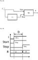
- FIG. 1 is a diagram illustrating the operation of a PUF. When stimulated by a data vector, called challenge C, the PUF generates a response R which is unique and which depends on the intrinsic manufacturing characteristics of the circuit.
- the different functionalities of a PUF can be implemented using devices that are more or less secure or costly in terms of performance/consumption/area, for example: fuses, secure memory with scrambling and encryption, set of sensors and devices for detecting attempts to read the secrets of the integrated circuit through physical access (reverse engineering), etc.
- PUFs are well known from the prior art and make it possible to measure one or more parameters (transistor threshold voltage, resistance of a metal line, parasitic capacitance, etc.) related to the manufacture of circuits integrated, which are likely to uniquely characterize each circuit.
- PUFs The implementation of PUFs is generally based on the analysis of delay variations to characterize and identify the circuit.
- a measurement of the frequency (number of events over a given period) of different oscillators is commonly used.
- RO-PUF for the English acronym “Ring Oscillator” PUF.
- This frequency measurement to be precise, requires counting the number of events over a long period. The response latency is therefore high.
- these measurements must also be differential (between two oscillators) and make a simple comparison (which oscillator is the fastest?). In the end, these solutions therefore require at least two oscillators to extract a single bit of entropy (solutions with 4 or 8 oscillators per bit are even considered to increase the stability of the measurements).
- the implementation of the PUF function comprises a step consisting in measuring, by means of a TDC converter, the difference between: - i ) the time of arrival of a first event of a signal at an input of the TDC converter and, - ii) the time of arrival of a second event of a signal at an input of the TDC converter, which second event is generated by the delay circuit.
- this type of solution reveals a certain determinism in the response of the PUF.
- This determinism stems in particular from the variations brought by the propagation paths between the source of the activation signal and the TDC, which variations influence the uniqueness of the unique datum (or response) generated by the PUF.
- the unique data (or responses) generated by several integrated circuits embedding this same PUF can then present a certain correlation favorable to attacks.
- An object of the invention is to remedy all or part of the aforementioned drawbacks.
- the claimed invention relates to a method and a circuit as defined in claims 1 and 6, respectively.
- the dependent claims relate to advantageous embodiments.
- the invention makes it possible to generate the unique data specific to the circuit, in an optimal manner, in particular in terms of speed and energy consumption.
- the propagation time of signals identical to manufacturing variations is measured very precisely, through one or more delay circuits.
- the propagation time differences in the delay circuit(s) make it possible in particular to construct a signature or another unique identifier of the circuit.
- the invention is based on the measurement of delays to characterize and identify the integrated circuit.
- a direct measurement of delays is carried out and not a measurement of frequency.
- the direct measurement of the delay is done using a TDC, without going through the frequency domain.
- the use of a very precise TDC is possible with a reasonable surface cost and consumption.
- This measurement is precise and fast (about 10 ns) and therefore makes it possible to gain one or two orders of magnitude on the latency of the other PUFs and in particular of the RO-PUFs.
- the invention also makes it possible to obtain stable measurements. Indeed, thanks to the rapid measurements of the delays, these are less subject to temperature variations, and more generally, are less sensitive to the conditions of use of the integrated circuit.
- Yet another aspect of the invention relates to the use of the integrated circuit to generate a random number.
- the method and the system which are the subject of the invention generate manipulations of physical elements, in particular signals (electrical or magnetic) and data, capable of being stored, transferred, combined, compared, ..., and making it possible to achieve a desired result.
- the “ unique datum ” specific to the integrated circuit and which is generated according to the method which is the subject of the invention can in particular be understood as: a unique identifier, a unique signature, an intrinsic characteristic of the integrated circuit, a response to a challenge, etc. . These terms are equivalent and can be used interchangeably in the present description.
- the implementation of the method which is the subject of the invention involves the use of a “ delay circuit ” of the integrated circuit.
- This term includes in particular any propagation path in the circuit, which may consist of passive elements (resistors, capacitors, inductors, etc.), active (transistors, diodes, etc.), complex elements (optoelectronics, electromechanical devices, etc.). ) or any assembly of these elements through one or more standard logic cells.
- This delay circuit is a source of entropy serving as a source of "fixation" of the variability of the manufacturing process and can be constructed in various ways. The differences in propagation delays of a signal can result from manufacturing variations of different elements of the integrated circuit.
- the choice of the delay circuit depends in particular on the technology used. To increase the efficiency of the method and reduce the size of the delay circuits, it is advantageous to maximize the variability/delay ratio.
- the implementation of the method which is the subject of the invention also involves the use of a TDC to extract/measure the entropy of the delay circuit.
- TDC To extract/measure the entropy of the delay circuit.
- STR Self-sequenced ring
- the TDC is used to measure the time between two events. These events can be generated in the form of electrical signals by different types of generators: ring oscillators, pulse generators, etc. In the remainder of the description, the events to be analyzed correspond to rising and/or falling edges. The invention however covers other types of events, for example one or more pieces of information (eg: number, letter, code, etc.) integrated into a signal. The TDC then measures the difference between the instants of arrival of this information.
- the TDC does not give the arrival time/time of each edge, but rather measures the spacing between the two edges. In other words, the TDC does not compare arrival times of two events, but times the difference in arrival between these two events. This dispenses with the use of a reference (or common clock) during the measurement. However, it is possible to use a TDC which retrieves the arrival time of each event (“timestamp” in English) in relation to a reference clock (internal to the PUF/TDC, to the system, or external) then to make the subtraction of the two values to obtain the value of the measured delay.
- FIG. 2a is a block diagram illustrating a device for implementing a method not covered by the claims, according to a first embodiment.
- the device comprises a delay circuit CR and a TDC. These elements allow the implementation of the PUF function of the integrated circuit.
- the TDC has two inputs: Start and Stop.
- An activation signal I is applied to the Start input of the TDC. This signal I corresponds to a first signal. This same signal I is applied to the input of the delay circuit CR.
- the Stop input of the TDC is connected to the output of the delay circuit CR.
- signal I presents a rising edge fm 0 .
- This rising edge fm 0 corresponds to the first event whose arrival time is measured by the TDC (at the Start input).
- Circuit CR induces a delay in signal I so that the rising edge will arrive with a delay D at the Stop input of the TDC.
- This rising edge fm 1 generated by the circuit CR corresponds to the second event whose arrival time is measured by the TDC (at the Stop input).
- the delayed signal at the output of the delay circuit CR corresponds to a second signal.
- the TDC will thus measure the delay D between the two rising edges—or the difference in the times of arrival of said rising edges ⁇ (fm 1 ; fm 0 ).
- the value of this delay D depends on the intrinsic manufacturing characteristics of the delay circuit CR and therefore of the integrated circuit.
- the embodiment of the picture 3a is similar to that of the figure 2a .
- the delay circuit CRi is however configured to invert the signal I (inverting delay; active on the rising edge of the activation signal I).
- the signal at the output of the circuit CRi then comprises a falling edge fd 1 which is delayed with respect to the rising edge fm 0 .
- the TDC will then measure the delay D between the rising edge fm 0 (first event of the first activation signal I arriving at the Start input) and the falling edge fd 1 (second event of the delayed signal arriving at the Stop input) - or the difference of the times of arrival of the rising edge fm 0 and of the falling edge fd 1 .
- the Start input of the TDC is in this case active on a rising edge and the Stop input active on a falling edge.
- the signal I could include a falling edge instead of the rising edge and that the TDC measures the instants of arrival of a falling edge at the Start input and a rising edge at the Stop input.
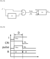
- an AND logic gate is interposed between the TDC and the delay circuit CRi.
- the signal I is applied to an input of the AND gate.
- the other input of the AND gate is connected to the output of the delay circuit CRi.
- the output of the AND gate is connected to the inputs Start and Stop TDC.
- the delay circuit CRi is configured to invert the signal I (inverting delay).
- the combination of the AND gate and the delay circuit CRi then makes it possible to generate a pulse - or signal referenced " Pulse " - having a rising edge fm 0 and a falling edge fd 1 (single pulse or single pulse generator) .
- the TDC measures the pulse width of the Pulse signal, i.e. the delay D between the rising edge fm 0 (first event of the Pulse signal arriving at the Start input) and the falling edge fd 1 (second event of the same Pulse signal arriving at the Stop input) of the Pulse signal - or the difference of the times of arrival of the rising edge fm 0 and of the falling edge fd 1 .
- the Start input of the TDC is in this case active on a rising edge and the Stop input active on a falling edge.
- the signal I could include a falling edge instead of the rising edge and that the TDC measures the instants of arrival of a falling edge at the Start input and a rising edge at the Stop input.
- the embodiment of the figure 5a corresponds to that of the figure 4a , the AND gate being however replaced by an exclusive NOR gate (XNOR gate).
- the activation signal I is a signal having a rising edge fm 0 and a falling edge fd 0 which follows it (the reverse being possible).
- the rising edge fm 0 is transformed into a falling edge fd 1
- the falling edge fd 0 is transformed into a rising edge fm 1 .
- the combination of the XNOR gate and the delay circuit CRi makes it possible to generate a double pulse - or Double Pulse signal (double pulse or double pulse generator). Each pulse has the same width and has a rising edge and a falling edge.
- the measurement performed by the TDC in the configuration of the figure 5a is more stable. Indeed, the redundancy of the measured values (width of two pulses greater than the width of a single pulse) makes it possible to increase the signal-to-noise ratio.
- the signal I is applied to an input of an AND gate.
- the output of the AND gate is connected on the one hand to the input of the delay circuit CRi (inverting delay) and on the other hand to the Start and Stop inputs of the TDC.
- the output of the delay circuit CRi is connected to the other input of the AND gate.
- the combination of the AND gate and the delay circuit Cri usually called ring oscillator, then makes it possible to generate multiple pulses - or Multi-Pulse signal - each having the same width and presenting a rising edge and a falling edge (generator multi-pulse).
- the TDC measures the width of each positive pulse of the Multi-Pulse signal, i.e. the delay D between a rising edge (first event of the Multi-Pulse signal arriving at the Start input) and the following falling edge ( second event of the same Multi-Pulse signal arriving at the Stop input) - or the difference in the times of arrival of the rising edge and the falling edge of each pulse in the high state. If the TDC is not reset between two successive high pulses, the value of its measurement (R) corresponds to the sum of the widths of these successive high pulses, or to the sum of the half-periods of oscillation of the Multi-Pulse signal . The redundancy of the measured values makes it possible to further increase the signal-to-noise ratio and the stability of the TDC measurement.
- the unique identifier R (calculated according to the modes of the figures 2a to 6a ), can be compared to a reference value.
- the latter is preferably a fixed, invariable value, and does not depend on the conditions of use of the circuit such as the temperature.
- the reference value is for example calculated theoretically (a priori), or estimated from the measurement of numerous samples (mean value).
- a comparator can be integrated into the integrated circuit so that the comparison is performed in situ, the reference value being stored in a memory of said circuit.
- the comparator can also be located outside the integrated circuit, in which case the comparison is carried out ex-situ, the reference value being stored in a memory remote from said circuit. This comparison can in particular be used in the context of monitoring and/or controlling manufacturing processes.
- the result of the comparison makes it possible, for example, to characterize the quality of manufacture of the integrated circuit and to deduce therefrom the compensations necessary to operate said circuit in an optimal manner (adjustment of the voltage or of the frequency for example).
- In situ comparison is used in this case.
- the result of the ex-situ comparison can be used to classify and sort the integrated circuits (ex: fast circuits or not) during manufacture, for example to sell them as different products, guaranteeing different performances.
- the device comprises several pulse generators G1, G2, ..., Gn (n being an integer equal to or greater than 2).
- These generators can be of the same type or of different types: simple pulse generator(s) of the type represented on the figure 4a ; double pulse generator(s) of the type shown in the figure 5a ; multi-pulse generator(s) of the type shown in the figure 6a , Or other.
- Each generator includes a delay circuit so that the signal generated by a generator has a first event and a second event generated by said delay circuit.
- the inputs of the generators G1, G2, ..., Gn are connected to the outputs of a demultiplexer DEMUX.
- the outputs of the generators G1, G2, ..., Gn are connected to the inputs of a multiplexer MUX.
- the DEMUX demultiplexer makes it possible to inject the activation signal I into one of the selected generators G1, G2, ..., Gn.
- This demultiplexer is however optional, the activation signal I being able to be injected simultaneously into each of the generators G1, G2, ..., Gn.
- This activation signal I is of the type described above.
- the MUX multiplexer sends the signal generated by the selected generator to the Start and Stop inputs of the TDC. Depending on its form, this signal comprises one or more first events (eg: rising edges) and one or more second events (eg: falling edges).
- the TDC measures the differences in the times of arrival of these events. By successively selecting all or part of the other generators G1, G2, ..., Gn, the TDC will be able to successively measure several delays D1, D2, ..., Dn which are transmitted successively to a functional block B. This is adapted to construct an answer R from one or more of these measures (2, 3, 4, ..., n).
- This response R is substantially more complex and more robust to attacks than those obtained according to the previous embodiments. It can for example be constructed by a mathematical operation applied to the measured delays D1, D2, ..., Dn: addition of the delays, comparison of the said delays with each other (which is the fastest?), subtraction of the said delays (what is the difference propagation time of two delays?), comparison or subtraction of said delays with a reference value, division of said delays (what is the relationship between two delays?); or by a multivariate mathematical function applied to said measured delays.
- the data generated by block B is particularly suitable for the identification and/or authentication of electronic equipment, the secure storage of encryption keys, the hardware-software coupling, the fight against counterfeiting, etc. Indeed, the data R can be expressed on several bits, becoming in fact more secure (unpredictable and non-reproducible). THE results of the mathematical operation applied to the successive measured delays D1, D2, ..., Dn can in particular be concatenated to construct unique data on a number of bits necessary for an application (for example 128 bits for an AES encryption key , 2048 bits for RSA encryption).
- the measurements made by the TDC are possibly dependent on the conditions of use of the circuit (for example the temperature or the supply voltage).
- the comparison of two measurements will make it possible to cancel out the variations induced by the conditions of use. This dispenses with the use of any means of compensation or analysis of these variations induced by the conditions of use.
- the embodiment of the figure 8 is similar to that of the figure 7 .
- the TDC comprises several inputs/outputs making it possible to simultaneously measure several delays D1, D2, ..., Dn and to transmit these measurements simultaneously to the functional block B.
- the latter comprises several inputs for this purpose.
- the measurements made by the TDC are in fact faster, because they are simultaneous.
- block B can process the different measurements simultaneously and no longer successively, and therefore generate a response R more quickly.
- This embodiment is also less sensitive to the conditions of use, since the measurements are made simultaneously.
- the TDC makes it possible to measure propagation times in each delay circuit. This measurement need not be absolute. It is therefore possible to simplify the TDC so as to obtain a relative value for each measurement. It is also possible to recover only a modulo or other part of the measurement (for example by applying a filtering of the least significant bits). This makes it possible to simplify the structure of the TDC to reduce its consumption and its surface, while maintaining a good entropy in the responses of the PUF.
- the device then becomes not only an identifier generator (PUF) but also a random number generator (TRNG).
- PAF identifier generator
- TRNG random number generator
- the signal-to-noise ratio is then increased. For example, it is possible to run the signal several times through the same delay circuit before making the measurement by the TDC. This reduces the impact of noise on the measurement. Indeed, the signal-to-noise ratio evolves in ⁇ N (N being the number of times that the same delay circuit is traversed by the signal).
- FIG. 9a to 11 Other embodiments using a "shaping" block are illustrated in the figures 9a to 11 . It is likely that a rising edge and a falling edge do not propagate at the same speed in the integrated circuit. Thus, the further the activation signal I is generated from the TDC, the more the generated pulse will reduce or increase in width. There is therefore a risk of introducing a direct correlation between the selected source and the response obtained (between the challenge and the response), so that an attacker can more easily predict the signature of the integrated circuit. Also, a formatting block MF is advantageously used to overcome this state of affairs.
- a first simple pulse generator G1 of the type described with reference to figure 4a , is used to generate a simple pulse - signal Pulse - having a rising edge fm 0 and a falling edge fd 0 .
- a second double pulse generator G2 of the type described with reference to figure 5a , transforms the Pulse signal into a double pulse - Double Pulse signal. Each pulse having a rising edge fm 1 , respectively fm 2 , and a falling edge fd 1 , respectively fd 2 .
- the MF block is installed upstream of the TDC and connected to its inputs.
- the MF block is suitable for transforming the double pulse into a single pulse - Pulse' signal.
- the block MF can in particular be active on the rising edges fm 1 , fm 2 (or falling edges fd 1 , fd 2 ).
- This transformation can for example be carried out by means of a flip-flop mounted as a divider, so as to pass only the rising edges (respectively falling) while inverting the even edges: the rising edge fm 1 is transmitted normally (it is the first event whose arrival time is measured by the TDC), the rising edge following fm 2 is inverted to be transformed into a falling edge (this is the second event whose arrival time is measured by the TDC). And so on.
- a multi-pulse generator G allows to generate multiple pulses - Multi-Pulse signal.
- the MF block is active on the rising (or falling) edges, so as to pass only the rising (respectively falling) edges while inverting the even edges ( Multi-Pulse' signal) .
- Each pulse of the Multi-Pulse signal has a rising edge (first event whose arrival time is measured by the TDC) and a falling edge (second event whose arrival time is measured by the TDC). This falling edge results from the transformation of a rising edge as explained previously.
- FIG 11 schematizes an architecture similar to that of the figure 7 , but where the MF block is installed between the MUX multiplexer and the TDC.
- Each of the generators G1, G2, ..., Gn generates a signal in the form of a double pulse or multiple pulses.
- the MF block transforms each signal so that it presents one or more first events (eg: rising edges) and one or more second events (eg: falling edges) whose arrival times will be measured by the TDC.
- the delays D1, D2, ..., Dn thus measured are then transmitted successively to the functional block B, the data R being generated in the same way as that described with reference to the figure 7 .
- Each input of the TDC is however associated with a shaping block MF1, MF2,..., MFn.
- Each signal (double pulse or multiple pulses) at the output of the multiplexer MUX is then transformed beforehand before entering the TDC.
- Each block MF1, MF2,..., MFn transforms the corresponding signal so that the latter presents one or more first events (e.g.: edges rising) and one or more second events (e.g. falling edges) whose arrival times will be measured by the TDC.
- the delays D1, D2, ..., Dn thus measured are then transmitted simultaneously to the functional block B, the data R being generated in the same way as that described with reference to the figure 8 .
- the shaping of the signal by the MF block, before its measurement by the TDC makes it possible to cancel, or at the very least to limit, any determinism in the response of the PUF. All the variations brought about by the propagation paths between the source of the activation signal I and the TDC are common to all the sources/challenges and do not influence the uniqueness of the response R. The latter is then more stable and more robust to attacks.
- the TDC measures positive pulses.
- the TDC can however be configured to measure negative pulses.
- one or more characteristics and/or steps exposed only in one embodiment can be generalized to the other embodiments.
- one or more features and/or steps set forth only in one embodiment may be combined with one or more other features and/or steps set forth only in another embodiment.
Landscapes
- Engineering & Computer Science (AREA)
- Computer Security & Cryptography (AREA)
- Theoretical Computer Science (AREA)
- Physics & Mathematics (AREA)
- General Physics & Mathematics (AREA)
- Computer Hardware Design (AREA)
- Mathematical Physics (AREA)
- Software Systems (AREA)
- General Engineering & Computer Science (AREA)
- Computer Networks & Wireless Communication (AREA)
- Signal Processing (AREA)
- Semiconductor Integrated Circuits (AREA)
- Tests Of Electronic Circuits (AREA)
- Synchronisation In Digital Transmission Systems (AREA)
Claims (7)
- Verfahren zum Generieren eines einer integrierten Schaltung aus Silicium eigenen Einzeldatenwerts (R), wobei der Datenwert durch die Anwendung einer physikalisch nicht klonbaren Funktion PUF der Schaltung generiert wird, welche Schaltung eine Verzögerungsschaltung (CR, CRi) aufweist, die Durchführung der Funktion PUF einen Schritt enthält, der darin besteht, mittels eines TDC-Wandlers die Differenz zu messen zwischen:- i) dem Ankunftszeitpunkt eines ersten Ereignisses eines Signals an einem Eingang (Start) des TDC-Wandlers und- ii) dem Ankunftszeitpunkt eines zweiten Ereignisses eines Signals an einem Eingang (Stop) des TDC-Wandlers, welches zweite Ereignis von der Verzögerungsschaltung (CR, CRi) generiert wird,dadurch gekennzeichnet, dass das Verfahren außerdem die Schritte enthält, die darin bestehen:- mittels mindestens eines die Verzögerungsschaltung (CR, CRi) aufweisenden Generators (G1, G2, G) ein Signal in Form eines Doppelimpulses oder vieler Impulse zu generieren,- das Signal so umzuformen, dass das erste Ereignis und das zweite Ereignis zum umgeformten Signal gehören.
- Verfahren nach Anspruch 1, wobei die integrierte Schaltung mehrere Verzögerungsschaltungen aufweist, wobei das Verfahren die Schritte enthält, die darin bestehen:- a) eine Vielzahl von Impulsgeneratoren (G1, G2, ..., Gn) zu formen, wobei jeder Generator eine der Verzögerungsschaltungen aufweist, wobei das von jedem Generator generierte Signal in Form eines Doppelimpulses oder vieler Impulse vorliegt,- b) unter der Vielzahl der Generatoren (G1, G2, ..., Gn) einen ersten Generator auszuwählen und ein erstes Signal ausgehend von dem ersten Generator zu generieren,- b1) das erste Signal so umzuformen, dass das erste Ereignis und das zweite Ereignis zum umgeformten Signal gehören,- c) mittels des TDC-Wandlers die Differenz zwischen dem Ankunftszeitpunkt des ersten Ereignisses des ersten umgeformten Signals und dem Ankunftszeitpunkt des zweiten Ereignisses des ersten umgeformten Signals zu messen,- d) die Schritte a) bis c) für alle oder einen Teil der anderen Generatoren (G1, G2, ..., Gn) zu wiederholen,- e) den der integrierten Schaltung eigenen Einzeldatenwert (R) abhängig von einer oder mehreren der aufeinanderfolgenden Messungen (D1, D2, ..., Dn) des TDC-Wandlers zu generieren.
- Verfahren nach Anspruch 1, wobei die integrierte Schaltung mehrere Verzögerungsschaltungen aufweist, wobei das Verfahren die Schritte enthält, die darin bestehen:- a) eine Vielzahl von Impulsgeneratoren (G1, G2, ..., Gn) zu formen, wobei jeder Generator eine der Verzögerungsschaltungen aufweist, wobei das von jedem Generator generierte Signal in Form eines Doppelimpulses oder vieler Impulse vorliegt,- b) gleichzeitig eine Vielzahl von Signalen ausgehend von den Generatoren zu generieren,- b1) jedes Signal so umzuformen, dass jedes umgeformte Signal ein erstes Ereignis und ein zweites Ereignis aufweist,- c) mittels des TDC-Wandlers die Differenz zwischen dem Ankunftszeitpunkt des ersten Ereignisses eines im Schritt b1) umgeformten Signals und dem Ankunftszeitpunkt des zweiten Ereignisses des umgeformten Signals zu messen, welche Messung gleichzeitig für die Vielzahl von im Schritt b1) umgeformten Signalen durchgeführt wird,- d) den der integrierten Schaltung eigenen Einzeldatenwert (R) abhängig von den gleichzeitigen Messungen (D1, D2, ..., Dn) des TDC-Wandlers zu generieren.
- Verfahren nach Anspruch 1, wobei der der integrierten Schaltung eigene Einzeldatenwert (R) durch eine mathematische Operation oder eine mathematische Funktion mit mehreren Variablen generiert wird, die an die verschiedenen Messungen des TDC-Wandlers angewendet wird.
- Verfahren nach einem der vorhergehenden Anspruche, wobei mehrere Male ein Signal durch die Verzögerungsschaltung geschickt wird, ehe die Messung durch den TDC-Wandler durchgeführt wird.
- Integrierte Schaltung aus Silicium, die eine physikalisch nicht klonbare Funktion PUF aufweist, die es ermöglicht, einen der Schaltung eigenen Einzeldatenwert (R) zu generieren, welche Schaltung aufweist:- eine Verzögerungsschaltung (CR, CRi),- einen TDC-Wandler zur Durchführung der Funktion PUF, welcher TDC-Wandler geeignet ist, zu messen:dadurch gekennzeichnet, dass die Schaltung außerdem enthält:- i) den Ankunftszeitpunkt eines ersten Ereignisses eines Signals an einem Eingang des TDC-Wandlers und- ii) den Ankunftszeitpunkt eines zweiten Ereignisses eines Signals an einem Eingang des TDC-Wandlers, welches zweite Ereignis von der Verzögerungsschaltung generiert wird,- mindestens einen die Verzögerungsschaltung (CR, CRi) aufweisenden Generator (G1, G2, G), welcher Generator geeignet ist, ein Signal in Form eines Doppelimpulses oder vieler Impulse zu generieren,- eine Einrichtung, um das Signal so umzuformen, dass das erste Ereignis und das zweite Ereignis zum umgeformten Signal gehören.
- Verwendung der integrierten Schaltung nach Anspruch 6 zum Generieren einer Zufallszahl.
Applications Claiming Priority (1)
| Application Number | Priority Date | Filing Date | Title |
|---|---|---|---|
| FR2000491A FR3106424B1 (fr) | 2020-01-17 | 2020-01-17 | Procédé pour générer une donnée unique propre à un circuit intégré en silicium |
Publications (2)
| Publication Number | Publication Date |
|---|---|
| EP3851995A1 EP3851995A1 (de) | 2021-07-21 |
| EP3851995B1 true EP3851995B1 (de) | 2023-02-22 |
Family
ID=70804701
Family Applications (1)
| Application Number | Title | Priority Date | Filing Date |
|---|---|---|---|
| EP21151895.6A Active EP3851995B1 (de) | 2020-01-17 | 2021-01-15 | Verfahren zur erzeugung eine einmalige daten, die für einen integrierten silikonkreis spezifisch ist |
Country Status (2)
| Country | Link |
|---|---|
| EP (1) | EP3851995B1 (de) |
| FR (1) | FR3106424B1 (de) |
Family Cites Families (5)
| Publication number | Priority date | Publication date | Assignee | Title |
|---|---|---|---|---|
| US7840803B2 (en) | 2002-04-16 | 2010-11-23 | Massachusetts Institute Of Technology | Authentication of integrated circuits |
| KR101366376B1 (ko) | 2006-01-24 | 2014-02-24 | 베라요, 인크. | 신호 제너레이터에 기반한 장치 보안 |
| FR2955394B1 (fr) | 2010-01-18 | 2012-01-06 | Inst Telecom Telecom Paristech | Circuit integre en silicium comportant une fonction physiquement non copiable, procede et systeme de test d'un tel circuit |
| EP2816756A1 (de) | 2013-06-18 | 2014-12-24 | Nagravision S.A. | Einmaliges kryptografisches Verfahren und einmalige kryptografische Vorrichtung mit einer physikalisch nicht wiederholbaren Funktion |
| EP3039550A4 (de) * | 2013-08-28 | 2017-10-18 | Stc.Unm | Systeme und verfahren zur ausnutzung von wegverzögerungsvariationen in einer schaltung und erzeugung von fehlertoleranten bitstrings |
-
2020
- 2020-01-17 FR FR2000491A patent/FR3106424B1/fr not_active Expired - Fee Related
-
2021
- 2021-01-15 EP EP21151895.6A patent/EP3851995B1/de active Active
Also Published As
| Publication number | Publication date |
|---|---|
| EP3851995A1 (de) | 2021-07-21 |
| FR3106424B1 (fr) | 2022-02-11 |
| FR3106424A1 (fr) | 2021-07-23 |
Similar Documents
| Publication | Publication Date | Title |
|---|---|---|
| EP3195296B1 (de) | System und verfahren zur sicherung eines elektronischen schaltkreises | |
| EP2526433B1 (de) | Integrierte siliciumschaltung mit einer physikalisch nicht reproduzierbaren funktion sowie verfahren und system zum testen solch einer schaltung | |
| EP2131495B1 (de) | Verzögerungsunempfindlicher asynchroner Schaltkreis mit Verzögerungseinschaltschaltkreis | |
| Kodýtek et al. | A design of ring oscillator based PUF on FPGA | |
| Stanzione et al. | CMOS silicon physical unclonable functions based on intrinsic process variability | |
| EP3242401B1 (de) | Schaltkreis zum zählen von impulsen | |
| EP2422206A1 (de) | Einrichtung zum überwachen des betriebs einer digitalen schaltung | |
| Claes et al. | Comparison of SRAM and FF PUF in 65nm technology | |
| EP3246943A1 (de) | Elektronische vorrichtung mit puf-basierter identifizierung | |
| EP3851995B1 (de) | Verfahren zur erzeugung eine einmalige daten, die für einen integrierten silikonkreis spezifisch ist | |
| WO2009118264A1 (fr) | Procede de protection de circuit de cryptographie programmable, et circuit protege par un tel procede | |
| FR2823398A1 (fr) | Extraction d'une donnee privee pour authentification d'un circuit integre | |
| FR2855286A1 (fr) | Transmission securisee de donnees entre deux modules | |
| WO2018087255A1 (fr) | Procédé et dispositif d'émission de données chiffrées, procédé et dispositif d'extraction de données | |
| FR2817361A1 (fr) | Generateur de signal aleatoire | |
| FR3111006A1 (fr) | Dispositif intégré de fonction physique non-clonable | |
| EP1521365A2 (de) | Vorrichtung zur digitalen Zeitverzögerung, digitaler Oszillator zur Erzeugung eines Taktsignals und Speicherschnittstelle | |
| EP2865158B1 (de) | Verfahren zur authentifizierung von an einer station eines digitalen telekommunikationssystems empfangenen datenpaketen | |
| EP1610463B1 (de) | Verifikation eines Bitstromes | |
| Du et al. | A novel relative frequency based ring oscillator physical unclonable function | |
| FR2885461A1 (fr) | Dispositif formant porte logique adaptee pour minimisee les differences de comportement electrique ou electromagnetique dans un circuit integre manipulant un secret | |
| EP1105997A1 (de) | Verfahren zur verbesserung eines statistischen tests | |
| Garay | On-board characterization and measurement of clock jitter used as source of randomness by TRNGs | |
| FR3137771A1 (fr) | Procédé et dispositif de qualification d'un générateur de nombre(s) aléatoire(s), et procédé de conception du générateur de nombre(s) aléatoire(s) | |
| Harding | EMBEDDED INCREASED ENTROPY PHYSICALLY UNCLONABLE FUNCTIONS |
Legal Events
| Date | Code | Title | Description |
|---|---|---|---|
| PUAI | Public reference made under article 153(3) epc to a published international application that has entered the european phase |
Free format text: ORIGINAL CODE: 0009012 |
|
| STAA | Information on the status of an ep patent application or granted ep patent |
Free format text: STATUS: THE APPLICATION HAS BEEN PUBLISHED |
|
| AK | Designated contracting states |
Kind code of ref document: A1 Designated state(s): AL AT BE BG CH CY CZ DE DK EE ES FI FR GB GR HR HU IE IS IT LI LT LU LV MC MK MT NL NO PL PT RO RS SE SI SK SM TR |
|
| STAA | Information on the status of an ep patent application or granted ep patent |
Free format text: STATUS: REQUEST FOR EXAMINATION WAS MADE |
|
| 17P | Request for examination filed |
Effective date: 20220119 |
|
| RBV | Designated contracting states (corrected) |
Designated state(s): AL AT BE BG CH CY CZ DE DK EE ES FI FR GB GR HR HU IE IS IT LI LT LU LV MC MK MT NL NO PL PT RO RS SE SI SK SM TR |
|
| GRAP | Despatch of communication of intention to grant a patent |
Free format text: ORIGINAL CODE: EPIDOSNIGR1 |
|
| STAA | Information on the status of an ep patent application or granted ep patent |
Free format text: STATUS: GRANT OF PATENT IS INTENDED |
|
| INTG | Intention to grant announced |
Effective date: 20220506 |
|
| GRAJ | Information related to disapproval of communication of intention to grant by the applicant or resumption of examination proceedings by the epo deleted |
Free format text: ORIGINAL CODE: EPIDOSDIGR1 |
|
| STAA | Information on the status of an ep patent application or granted ep patent |
Free format text: STATUS: REQUEST FOR EXAMINATION WAS MADE |
|
| INTC | Intention to grant announced (deleted) | ||
| GRAP | Despatch of communication of intention to grant a patent |
Free format text: ORIGINAL CODE: EPIDOSNIGR1 |
|
| STAA | Information on the status of an ep patent application or granted ep patent |
Free format text: STATUS: GRANT OF PATENT IS INTENDED |
|
| RIC1 | Information provided on ipc code assigned before grant |
Ipc: H04L 9/32 20060101ALI20220930BHEP Ipc: G09C 1/00 20060101ALI20220930BHEP Ipc: G06F 21/73 20130101AFI20220930BHEP |
|
| INTG | Intention to grant announced |
Effective date: 20221020 |
|
| GRAS | Grant fee paid |
Free format text: ORIGINAL CODE: EPIDOSNIGR3 |
|
| GRAA | (expected) grant |
Free format text: ORIGINAL CODE: 0009210 |
|
| STAA | Information on the status of an ep patent application or granted ep patent |
Free format text: STATUS: THE PATENT HAS BEEN GRANTED |
|
| AK | Designated contracting states |
Kind code of ref document: B1 Designated state(s): AL AT BE BG CH CY CZ DE DK EE ES FI FR GB GR HR HU IE IS IT LI LT LU LV MC MK MT NL NO PL PT RO RS SE SI SK SM TR |
|
| REG | Reference to a national code |
Ref country code: GB Ref legal event code: FG4D Free format text: NOT ENGLISH |
|
| REG | Reference to a national code |
Ref country code: CH Ref legal event code: EP |
|
| REG | Reference to a national code |
Ref country code: DE Ref legal event code: R096 Ref document number: 602021001423 Country of ref document: DE |
|
| REG | Reference to a national code |
Ref country code: AT Ref legal event code: REF Ref document number: 1550000 Country of ref document: AT Kind code of ref document: T Effective date: 20230315 Ref country code: IE Ref legal event code: FG4D Free format text: LANGUAGE OF EP DOCUMENT: FRENCH |
|
| REG | Reference to a national code |
Ref country code: LT Ref legal event code: MG9D |
|
| REG | Reference to a national code |
Ref country code: NL Ref legal event code: MP Effective date: 20230222 |
|
| REG | Reference to a national code |
Ref country code: AT Ref legal event code: MK05 Ref document number: 1550000 Country of ref document: AT Kind code of ref document: T Effective date: 20230222 |
|
| PG25 | Lapsed in a contracting state [announced via postgrant information from national office to epo] |
Ref country code: RS Free format text: LAPSE BECAUSE OF FAILURE TO SUBMIT A TRANSLATION OF THE DESCRIPTION OR TO PAY THE FEE WITHIN THE PRESCRIBED TIME-LIMIT Effective date: 20230222 Ref country code: PT Free format text: LAPSE BECAUSE OF FAILURE TO SUBMIT A TRANSLATION OF THE DESCRIPTION OR TO PAY THE FEE WITHIN THE PRESCRIBED TIME-LIMIT Effective date: 20230622 Ref country code: NO Free format text: LAPSE BECAUSE OF FAILURE TO SUBMIT A TRANSLATION OF THE DESCRIPTION OR TO PAY THE FEE WITHIN THE PRESCRIBED TIME-LIMIT Effective date: 20230522 Ref country code: NL Free format text: LAPSE BECAUSE OF FAILURE TO SUBMIT A TRANSLATION OF THE DESCRIPTION OR TO PAY THE FEE WITHIN THE PRESCRIBED TIME-LIMIT Effective date: 20230222 Ref country code: LV Free format text: LAPSE BECAUSE OF FAILURE TO SUBMIT A TRANSLATION OF THE DESCRIPTION OR TO PAY THE FEE WITHIN THE PRESCRIBED TIME-LIMIT Effective date: 20230222 Ref country code: LT Free format text: LAPSE BECAUSE OF FAILURE TO SUBMIT A TRANSLATION OF THE DESCRIPTION OR TO PAY THE FEE WITHIN THE PRESCRIBED TIME-LIMIT Effective date: 20230222 Ref country code: HR Free format text: LAPSE BECAUSE OF FAILURE TO SUBMIT A TRANSLATION OF THE DESCRIPTION OR TO PAY THE FEE WITHIN THE PRESCRIBED TIME-LIMIT Effective date: 20230222 Ref country code: ES Free format text: LAPSE BECAUSE OF FAILURE TO SUBMIT A TRANSLATION OF THE DESCRIPTION OR TO PAY THE FEE WITHIN THE PRESCRIBED TIME-LIMIT Effective date: 20230222 Ref country code: AT Free format text: LAPSE BECAUSE OF FAILURE TO SUBMIT A TRANSLATION OF THE DESCRIPTION OR TO PAY THE FEE WITHIN THE PRESCRIBED TIME-LIMIT Effective date: 20230222 |
|
| PG25 | Lapsed in a contracting state [announced via postgrant information from national office to epo] |
Ref country code: SE Free format text: LAPSE BECAUSE OF FAILURE TO SUBMIT A TRANSLATION OF THE DESCRIPTION OR TO PAY THE FEE WITHIN THE PRESCRIBED TIME-LIMIT Effective date: 20230222 Ref country code: PL Free format text: LAPSE BECAUSE OF FAILURE TO SUBMIT A TRANSLATION OF THE DESCRIPTION OR TO PAY THE FEE WITHIN THE PRESCRIBED TIME-LIMIT Effective date: 20230222 Ref country code: IS Free format text: LAPSE BECAUSE OF FAILURE TO SUBMIT A TRANSLATION OF THE DESCRIPTION OR TO PAY THE FEE WITHIN THE PRESCRIBED TIME-LIMIT Effective date: 20230622 Ref country code: GR Free format text: LAPSE BECAUSE OF FAILURE TO SUBMIT A TRANSLATION OF THE DESCRIPTION OR TO PAY THE FEE WITHIN THE PRESCRIBED TIME-LIMIT Effective date: 20230523 Ref country code: FI Free format text: LAPSE BECAUSE OF FAILURE TO SUBMIT A TRANSLATION OF THE DESCRIPTION OR TO PAY THE FEE WITHIN THE PRESCRIBED TIME-LIMIT Effective date: 20230222 |
|
| PG25 | Lapsed in a contracting state [announced via postgrant information from national office to epo] |
Ref country code: SM Free format text: LAPSE BECAUSE OF FAILURE TO SUBMIT A TRANSLATION OF THE DESCRIPTION OR TO PAY THE FEE WITHIN THE PRESCRIBED TIME-LIMIT Effective date: 20230222 Ref country code: RO Free format text: LAPSE BECAUSE OF FAILURE TO SUBMIT A TRANSLATION OF THE DESCRIPTION OR TO PAY THE FEE WITHIN THE PRESCRIBED TIME-LIMIT Effective date: 20230222 Ref country code: EE Free format text: LAPSE BECAUSE OF FAILURE TO SUBMIT A TRANSLATION OF THE DESCRIPTION OR TO PAY THE FEE WITHIN THE PRESCRIBED TIME-LIMIT Effective date: 20230222 Ref country code: DK Free format text: LAPSE BECAUSE OF FAILURE TO SUBMIT A TRANSLATION OF THE DESCRIPTION OR TO PAY THE FEE WITHIN THE PRESCRIBED TIME-LIMIT Effective date: 20230222 Ref country code: CZ Free format text: LAPSE BECAUSE OF FAILURE TO SUBMIT A TRANSLATION OF THE DESCRIPTION OR TO PAY THE FEE WITHIN THE PRESCRIBED TIME-LIMIT Effective date: 20230222 |
|
| REG | Reference to a national code |
Ref country code: DE Ref legal event code: R097 Ref document number: 602021001423 Country of ref document: DE |
|
| PG25 | Lapsed in a contracting state [announced via postgrant information from national office to epo] |
Ref country code: SK Free format text: LAPSE BECAUSE OF FAILURE TO SUBMIT A TRANSLATION OF THE DESCRIPTION OR TO PAY THE FEE WITHIN THE PRESCRIBED TIME-LIMIT Effective date: 20230222 |
|
| PLBE | No opposition filed within time limit |
Free format text: ORIGINAL CODE: 0009261 |
|
| STAA | Information on the status of an ep patent application or granted ep patent |
Free format text: STATUS: NO OPPOSITION FILED WITHIN TIME LIMIT |
|
| 26N | No opposition filed |
Effective date: 20231123 |
|
| PG25 | Lapsed in a contracting state [announced via postgrant information from national office to epo] |
Ref country code: SI Free format text: LAPSE BECAUSE OF FAILURE TO SUBMIT A TRANSLATION OF THE DESCRIPTION OR TO PAY THE FEE WITHIN THE PRESCRIBED TIME-LIMIT Effective date: 20230222 |
|
| PG25 | Lapsed in a contracting state [announced via postgrant information from national office to epo] |
Ref country code: IT Free format text: LAPSE BECAUSE OF FAILURE TO SUBMIT A TRANSLATION OF THE DESCRIPTION OR TO PAY THE FEE WITHIN THE PRESCRIBED TIME-LIMIT Effective date: 20230222 |
|
| PG25 | Lapsed in a contracting state [announced via postgrant information from national office to epo] |
Ref country code: MC Free format text: LAPSE BECAUSE OF FAILURE TO SUBMIT A TRANSLATION OF THE DESCRIPTION OR TO PAY THE FEE WITHIN THE PRESCRIBED TIME-LIMIT Effective date: 20230222 |
|
| PG25 | Lapsed in a contracting state [announced via postgrant information from national office to epo] |
Ref country code: MC Free format text: LAPSE BECAUSE OF FAILURE TO SUBMIT A TRANSLATION OF THE DESCRIPTION OR TO PAY THE FEE WITHIN THE PRESCRIBED TIME-LIMIT Effective date: 20230222 |
|
| PG25 | Lapsed in a contracting state [announced via postgrant information from national office to epo] |
Ref country code: LU Free format text: LAPSE BECAUSE OF NON-PAYMENT OF DUE FEES Effective date: 20240115 |
|
| PG25 | Lapsed in a contracting state [announced via postgrant information from national office to epo] |
Ref country code: LU Free format text: LAPSE BECAUSE OF NON-PAYMENT OF DUE FEES Effective date: 20240115 |
|
| PG25 | Lapsed in a contracting state [announced via postgrant information from national office to epo] |
Ref country code: BG Free format text: LAPSE BECAUSE OF FAILURE TO SUBMIT A TRANSLATION OF THE DESCRIPTION OR TO PAY THE FEE WITHIN THE PRESCRIBED TIME-LIMIT Effective date: 20230222 |
|
| PG25 | Lapsed in a contracting state [announced via postgrant information from national office to epo] |
Ref country code: BG Free format text: LAPSE BECAUSE OF FAILURE TO SUBMIT A TRANSLATION OF THE DESCRIPTION OR TO PAY THE FEE WITHIN THE PRESCRIBED TIME-LIMIT Effective date: 20230222 |
|
| PG25 | Lapsed in a contracting state [announced via postgrant information from national office to epo] |
Ref country code: IE Free format text: LAPSE BECAUSE OF NON-PAYMENT OF DUE FEES Effective date: 20240115 |
|
| PG25 | Lapsed in a contracting state [announced via postgrant information from national office to epo] |
Ref country code: IE Free format text: LAPSE BECAUSE OF NON-PAYMENT OF DUE FEES Effective date: 20240115 |
|
| PG25 | Lapsed in a contracting state [announced via postgrant information from national office to epo] |
Ref country code: CY Free format text: LAPSE BECAUSE OF FAILURE TO SUBMIT A TRANSLATION OF THE DESCRIPTION OR TO PAY THE FEE WITHIN THE PRESCRIBED TIME-LIMIT; INVALID AB INITIO Effective date: 20210115 |
|
| PG25 | Lapsed in a contracting state [announced via postgrant information from national office to epo] |
Ref country code: HU Free format text: LAPSE BECAUSE OF FAILURE TO SUBMIT A TRANSLATION OF THE DESCRIPTION OR TO PAY THE FEE WITHIN THE PRESCRIBED TIME-LIMIT; INVALID AB INITIO Effective date: 20210115 |
|
| PG25 | Lapsed in a contracting state [announced via postgrant information from national office to epo] |
Ref country code: TR Free format text: LAPSE BECAUSE OF FAILURE TO SUBMIT A TRANSLATION OF THE DESCRIPTION OR TO PAY THE FEE WITHIN THE PRESCRIBED TIME-LIMIT Effective date: 20230222 |
|
| REG | Reference to a national code |
Ref country code: CH Ref legal event code: U11 Free format text: ST27 STATUS EVENT CODE: U-0-0-U10-U11 (AS PROVIDED BY THE NATIONAL OFFICE) Effective date: 20260223 |
|
| PGFP | Annual fee paid to national office [announced via postgrant information from national office to epo] |
Ref country code: GB Payment date: 20260219 Year of fee payment: 6 |
|
| PGFP | Annual fee paid to national office [announced via postgrant information from national office to epo] |
Ref country code: DE Payment date: 20260206 Year of fee payment: 6 |
|
| PGFP | Annual fee paid to national office [announced via postgrant information from national office to epo] |
Ref country code: BE Payment date: 20260130 Year of fee payment: 6 |
|
| PGFP | Annual fee paid to national office [announced via postgrant information from national office to epo] |
Ref country code: FR Payment date: 20260128 Year of fee payment: 6 |
|
| PGFP | Annual fee paid to national office [announced via postgrant information from national office to epo] |
Ref country code: CH Payment date: 20260223 Year of fee payment: 6 |