EP3848962A2 - Semiconductor package having re-distribution layer structure on substrate component - Google Patents
Semiconductor package having re-distribution layer structure on substrate component Download PDFInfo
- Publication number
- EP3848962A2 EP3848962A2 EP20213349.2A EP20213349A EP3848962A2 EP 3848962 A2 EP3848962 A2 EP 3848962A2 EP 20213349 A EP20213349 A EP 20213349A EP 3848962 A2 EP3848962 A2 EP 3848962A2
- Authority
- EP
- European Patent Office
- Prior art keywords
- semiconductor package
- substrate component
- rdl
- rdl structure
- encapsulant
- Prior art date
- Legal status (The legal status is an assumption and is not a legal conclusion. Google has not performed a legal analysis and makes no representation as to the accuracy of the status listed.)
- Granted
Links
Images








Classifications
-
- H—ELECTRICITY
- H10—SEMICONDUCTOR DEVICES; ELECTRIC SOLID-STATE DEVICES NOT OTHERWISE PROVIDED FOR
- H10W—GENERIC PACKAGES, INTERCONNECTIONS, CONNECTORS OR OTHER CONSTRUCTIONAL DETAILS OF DEVICES COVERED BY CLASS H10
- H10W70/00—Package substrates; Interposers; Redistribution layers [RDL]
- H10W70/60—Insulating or insulated package substrates; Interposers; Redistribution layers
- H10W70/611—Insulating or insulated package substrates; Interposers; Redistribution layers for connecting multiple chips together
-
- H—ELECTRICITY
- H10—SEMICONDUCTOR DEVICES; ELECTRIC SOLID-STATE DEVICES NOT OTHERWISE PROVIDED FOR
- H10W—GENERIC PACKAGES, INTERCONNECTIONS, CONNECTORS OR OTHER CONSTRUCTIONAL DETAILS OF DEVICES COVERED BY CLASS H10
- H10W74/00—Encapsulations, e.g. protective coatings
- H10W74/10—Encapsulations, e.g. protective coatings characterised by their shape or disposition
- H10W74/111—Encapsulations, e.g. protective coatings characterised by their shape or disposition the semiconductor body being completely enclosed
- H10W74/114—Encapsulations, e.g. protective coatings characterised by their shape or disposition the semiconductor body being completely enclosed by a substrate and the encapsulations
- H10W74/117—Encapsulations, e.g. protective coatings characterised by their shape or disposition the semiconductor body being completely enclosed by a substrate and the encapsulations the substrate having spherical bumps for external connection
-
- H—ELECTRICITY
- H10—SEMICONDUCTOR DEVICES; ELECTRIC SOLID-STATE DEVICES NOT OTHERWISE PROVIDED FOR
- H10W—GENERIC PACKAGES, INTERCONNECTIONS, CONNECTORS OR OTHER CONSTRUCTIONAL DETAILS OF DEVICES COVERED BY CLASS H10
- H10W42/00—Arrangements for protection of devices
- H10W42/121—Arrangements for protection of devices protecting against mechanical damage
-
- H—ELECTRICITY
- H10—SEMICONDUCTOR DEVICES; ELECTRIC SOLID-STATE DEVICES NOT OTHERWISE PROVIDED FOR
- H10W—GENERIC PACKAGES, INTERCONNECTIONS, CONNECTORS OR OTHER CONSTRUCTIONAL DETAILS OF DEVICES COVERED BY CLASS H10
- H10W70/00—Package substrates; Interposers; Redistribution layers [RDL]
- H10W70/60—Insulating or insulated package substrates; Interposers; Redistribution layers
- H10W70/67—Insulating or insulated package substrates; Interposers; Redistribution layers characterised by their insulating layers or insulating parts
- H10W70/68—Shapes or dispositions thereof
- H10W70/685—Shapes or dispositions thereof comprising multiple insulating layers
-
- H—ELECTRICITY
- H10—SEMICONDUCTOR DEVICES; ELECTRIC SOLID-STATE DEVICES NOT OTHERWISE PROVIDED FOR
- H10W—GENERIC PACKAGES, INTERCONNECTIONS, CONNECTORS OR OTHER CONSTRUCTIONAL DETAILS OF DEVICES COVERED BY CLASS H10
- H10W74/00—Encapsulations, e.g. protective coatings
- H10W74/01—Manufacture or treatment
- H10W74/019—Manufacture or treatment using temporary auxiliary substrates
-
- H—ELECTRICITY
- H10—SEMICONDUCTOR DEVICES; ELECTRIC SOLID-STATE DEVICES NOT OTHERWISE PROVIDED FOR
- H10W—GENERIC PACKAGES, INTERCONNECTIONS, CONNECTORS OR OTHER CONSTRUCTIONAL DETAILS OF DEVICES COVERED BY CLASS H10
- H10W90/00—Package configurations
-
- H—ELECTRICITY
- H10—SEMICONDUCTOR DEVICES; ELECTRIC SOLID-STATE DEVICES NOT OTHERWISE PROVIDED FOR
- H10W—GENERIC PACKAGES, INTERCONNECTIONS, CONNECTORS OR OTHER CONSTRUCTIONAL DETAILS OF DEVICES COVERED BY CLASS H10
- H10W90/00—Package configurations
- H10W90/401—Package configurations characterised by multiple insulating or insulated package substrates, interposers or RDLs
-
- H—ELECTRICITY
- H10—SEMICONDUCTOR DEVICES; ELECTRIC SOLID-STATE DEVICES NOT OTHERWISE PROVIDED FOR
- H10W—GENERIC PACKAGES, INTERCONNECTIONS, CONNECTORS OR OTHER CONSTRUCTIONAL DETAILS OF DEVICES COVERED BY CLASS H10
- H10W90/00—Package configurations
- H10W90/701—Package configurations characterised by the relative positions of pads or connectors relative to package parts
-
- H—ELECTRICITY
- H10—SEMICONDUCTOR DEVICES; ELECTRIC SOLID-STATE DEVICES NOT OTHERWISE PROVIDED FOR
- H10P—GENERIC PROCESSES OR APPARATUS FOR THE MANUFACTURE OR TREATMENT OF DEVICES COVERED BY CLASS H10
- H10P72/00—Handling or holding of wafers, substrates or devices during manufacture or treatment thereof
- H10P72/70—Handling or holding of wafers, substrates or devices during manufacture or treatment thereof for supporting or gripping
- H10P72/74—Handling or holding of wafers, substrates or devices during manufacture or treatment thereof for supporting or gripping using temporarily an auxiliary support
-
- H—ELECTRICITY
- H10—SEMICONDUCTOR DEVICES; ELECTRIC SOLID-STATE DEVICES NOT OTHERWISE PROVIDED FOR
- H10W—GENERIC PACKAGES, INTERCONNECTIONS, CONNECTORS OR OTHER CONSTRUCTIONAL DETAILS OF DEVICES COVERED BY CLASS H10
- H10W70/00—Package substrates; Interposers; Redistribution layers [RDL]
- H10W70/60—Insulating or insulated package substrates; Interposers; Redistribution layers
-
- H—ELECTRICITY
- H10—SEMICONDUCTOR DEVICES; ELECTRIC SOLID-STATE DEVICES NOT OTHERWISE PROVIDED FOR
- H10W—GENERIC PACKAGES, INTERCONNECTIONS, CONNECTORS OR OTHER CONSTRUCTIONAL DETAILS OF DEVICES COVERED BY CLASS H10
- H10W70/00—Package substrates; Interposers; Redistribution layers [RDL]
- H10W70/60—Insulating or insulated package substrates; Interposers; Redistribution layers
- H10W70/62—Insulating or insulated package substrates; Interposers; Redistribution layers characterised by their interconnections
- H10W70/63—Vias, e.g. via plugs
- H10W70/635—Through-vias
-
- H—ELECTRICITY
- H10—SEMICONDUCTOR DEVICES; ELECTRIC SOLID-STATE DEVICES NOT OTHERWISE PROVIDED FOR
- H10W—GENERIC PACKAGES, INTERCONNECTIONS, CONNECTORS OR OTHER CONSTRUCTIONAL DETAILS OF DEVICES COVERED BY CLASS H10
- H10W70/00—Package substrates; Interposers; Redistribution layers [RDL]
- H10W70/60—Insulating or insulated package substrates; Interposers; Redistribution layers
- H10W70/62—Insulating or insulated package substrates; Interposers; Redistribution layers characterised by their interconnections
- H10W70/65—Shapes or dispositions of interconnections
-
- H—ELECTRICITY
- H10—SEMICONDUCTOR DEVICES; ELECTRIC SOLID-STATE DEVICES NOT OTHERWISE PROVIDED FOR
- H10W—GENERIC PACKAGES, INTERCONNECTIONS, CONNECTORS OR OTHER CONSTRUCTIONAL DETAILS OF DEVICES COVERED BY CLASS H10
- H10W70/00—Package substrates; Interposers; Redistribution layers [RDL]
- H10W70/60—Insulating or insulated package substrates; Interposers; Redistribution layers
- H10W70/62—Insulating or insulated package substrates; Interposers; Redistribution layers characterised by their interconnections
- H10W70/65—Shapes or dispositions of interconnections
- H10W70/652—Cross-sectional shapes
-
- H—ELECTRICITY
- H10—SEMICONDUCTOR DEVICES; ELECTRIC SOLID-STATE DEVICES NOT OTHERWISE PROVIDED FOR
- H10W—GENERIC PACKAGES, INTERCONNECTIONS, CONNECTORS OR OTHER CONSTRUCTIONAL DETAILS OF DEVICES COVERED BY CLASS H10
- H10W72/00—Interconnections or connectors in packages
- H10W72/01—Manufacture or treatment
- H10W72/012—Manufacture or treatment of bump connectors, dummy bumps or thermal bumps
- H10W72/01212—Manufacture or treatment of bump connectors, dummy bumps or thermal bumps at a different location than on the final device, e.g. forming as prepeg
-
- H—ELECTRICITY
- H10—SEMICONDUCTOR DEVICES; ELECTRIC SOLID-STATE DEVICES NOT OTHERWISE PROVIDED FOR
- H10W—GENERIC PACKAGES, INTERCONNECTIONS, CONNECTORS OR OTHER CONSTRUCTIONAL DETAILS OF DEVICES COVERED BY CLASS H10
- H10W72/00—Interconnections or connectors in packages
- H10W72/20—Bump connectors, e.g. solder bumps or copper pillars; Dummy bumps; Thermal bumps
- H10W72/221—Structures or relative sizes
-
- H—ELECTRICITY
- H10—SEMICONDUCTOR DEVICES; ELECTRIC SOLID-STATE DEVICES NOT OTHERWISE PROVIDED FOR
- H10W—GENERIC PACKAGES, INTERCONNECTIONS, CONNECTORS OR OTHER CONSTRUCTIONAL DETAILS OF DEVICES COVERED BY CLASS H10
- H10W72/00—Interconnections or connectors in packages
- H10W72/20—Bump connectors, e.g. solder bumps or copper pillars; Dummy bumps; Thermal bumps
- H10W72/251—Materials
- H10W72/252—Materials comprising solid metals or solid metalloids, e.g. PbSn, Ag or Cu
-
- H—ELECTRICITY
- H10—SEMICONDUCTOR DEVICES; ELECTRIC SOLID-STATE DEVICES NOT OTHERWISE PROVIDED FOR
- H10W—GENERIC PACKAGES, INTERCONNECTIONS, CONNECTORS OR OTHER CONSTRUCTIONAL DETAILS OF DEVICES COVERED BY CLASS H10
- H10W74/00—Encapsulations, e.g. protective coatings
- H10W74/01—Manufacture or treatment
- H10W74/014—Manufacture or treatment using batch processing
-
- H—ELECTRICITY
- H10—SEMICONDUCTOR DEVICES; ELECTRIC SOLID-STATE DEVICES NOT OTHERWISE PROVIDED FOR
- H10W—GENERIC PACKAGES, INTERCONNECTIONS, CONNECTORS OR OTHER CONSTRUCTIONAL DETAILS OF DEVICES COVERED BY CLASS H10
- H10W90/00—Package configurations
- H10W90/701—Package configurations characterised by the relative positions of pads or connectors relative to package parts
- H10W90/721—Package configurations characterised by the relative positions of pads or connectors relative to package parts of bump connectors
- H10W90/724—Package configurations characterised by the relative positions of pads or connectors relative to package parts of bump connectors between a chip and a stacked insulating package substrate, interposer or RDL
Definitions
- the encapsulant is in direct contact with an upper portion of each of the BGA balls.
- the RDL structure has an RDL pitch of line/space (L/S) ⁇ 2/2 ⁇ m.
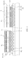
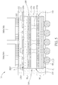
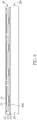
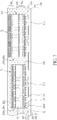
- FIG. 1 to FIG. 5 are schematic, cross-sectional diagrams showing an exemplary method for fabricating a semiconductor package with a buried substrate component according to one embodiment of the invention, wherein FIG. 5 shows a cross section of an individual semiconductor package after singulation and de-carrier.
- the semiconductor package 10 may be a multi-die package and comprises the cored substrate component 100 having a core layer 101, which is composed of a material such as bismaleimide-triazine resin or the like, and build-up interconnect structure BL 1 and BL 2 disposed on two opposite surfaces of the core layer 101, respectively.
- a plurality of plated through holes (PTHs) 101p may be provided in the core layer 101 for electrically connecting the build-up interconnect structure BL 1 with the build-up interconnect structure BL 2 .
- the cored substrate component 100 may be a 2-layer, 4-layer, or 6-layer substrate, but is not limited thereto.
- the first surface S 1 of the cored substrate component 100 is flush with the upper surface 120a of the encapsulant 120.
- the RDL structure 130 is formed on the first surface S 1 of the cored substrate component 100 and on the upper surface 120a of the encapsulant 120.
- the RDL structure 130 comprises dielectric layers 131, traces 132 in the dielectric layers 131, and re-distributed bonding pads RBP for connecting with an integrated circuit chip or die.
- the dielectric layers 131 may comprise silicon oxide, silicon oxy-nitride, silicon nitride, and/or low-k dielectric layers, but is not limited thereto.
- the RDL structure 130 can have a tighter RDL pitch (i.e., L/S ⁇ 2/2 ⁇ m).
- a plurality of cored substrate components (or BGA substrate components) 100 is distributed on the RDL structure 130.
- the cored substrate component 100a may have a thickness that is smaller than that of the cored substrate component 100b due to the process variation.
- Each of the cored substrates 100 has a first surface S 1 for electrically coupling with at least one chip or electronic device thereon and a second surface S 2 for electrically coupling with an external circuitry such as a printed circuit board or a system board.
- the cored substrate components 100a and 100b are over-molded by an encapsulant 120 by performing a molding process.
- the molding process may be compression molding.
- the molding process may be performed by dispensing, but is not limited thereto.
- the encapsulant 120 may comprise a molding compound comprising an epoxy or a resin, but is not limited thereto.
- the encapsulant 120 may surround each of the cored substrate components 100 and may fill into the gap between each of the cored substrate components 100 and the carrier 200.
- the second surface S 2 that faces upwardly at this point is also covered with the encapsulant 120 and each of the solder balls 110 is at least partially revealed.
- the dielectric layers 131 may comprise silicon oxide, silicon oxy-nitride, silicon nitride, and/or low-k dielectric layers, but is not limited thereto.
- the RDL structure 130 can have a tighter RDL pitch (i.e., L/S ⁇ 2/2 ⁇ m).
- a molding process is omitted. That is, the first surface S 1 , the second surface S 2 , and the sidewall surface SW of the cored substrate component 100 are not covered with an encapsulant. Therefore, the warpage problem of the semiconductor package 40 can be improved.
Landscapes
- Structures Or Materials For Encapsulating Or Coating Semiconductor Devices Or Solid State Devices (AREA)
- Production Of Multi-Layered Print Wiring Board (AREA)
- Wire Bonding (AREA)
- Control And Other Processes For Unpacking Of Materials (AREA)
- Physics & Mathematics (AREA)
- Geometry (AREA)
- Encapsulation Of And Coatings For Semiconductor Or Solid State Devices (AREA)
Abstract
Description
- This application claims priority from
U.S. provisional application No. 62/959,336 filed on January 10, 2020 - The present disclosure relates generally to the field of semiconductor packaging. More particularly, the present disclosure relates to a cost-effective chip on RDL on substrate (CRoS) package and fabrication methods thereof.
- Emerging markets are always driving demand for higher performance, higher bandwidth, lower power consumption as well as increasing functionality in mobile applications. Packaging technology has become more challenging and complicated than ever before, driving advance silicon nodes, finer bump pitch as well as finer line width and spacing substrate manufacturing capabilities to satisfy the increasing requirements in semiconductor industry.
- Although emerging markets are driving advanced technologies in high performance mobile devices, assembly cost is still the major issue to be addressed. As the substrate cost is always the significant factor in a flip chip package, flip chip assembly with a low cost substrate has become a hot topic in the industry.
- A prior art method for forming a semiconductor package generally involves the following steps. First, multiple cored substrate components are mounted on a carrier. Each of the cored substrate components has a plurality of copper pillars disposed on a chip side thereof. Subsequently, the multiple cored substrate components are over-molded and the end surface of each of the plurality of copper pillars is exposed by grinding or polishing. A re-distribution layer (RDL) is then fabricated on the top surface of the molding compound and is electrically coupled to the cored substrate component through the plurality of pillars. Thereafter, multiple integrated circuit (IC) dies are mounted on the RDL.
- The above-described prior art has several drawbacks. For example, to compensate the thickness variation of the cored substrate components, an adequate height (>150µm) of the plurality of copper posts is required. However, the tall copper pillars may reduce latency and incur high cost of copper plating. The diameter size of the copper pillars is constrained because of the shear force demand. Further, the design rule of routing is constrained by the positions of the plurality of copper posts and the dimension of each copper post. The RDL may suffer from package warping due to the over-molding process.
- It is an object of the invention to provide an improved semiconductor package with chip on RDL on substrate (CRoS) configuration in order to solve the above-mentioned prior art problems or shortcomings. Semiconductor packages according to the invention are defined in the independent claims. The dependent claims define preferred embodiments thereof.
- One aspect of the invention provides a semiconductor package including a substrate component comprising a first surface, a second surface opposite to the first surface, and a sidewall surface extending between the first surface and the second surface; a re-distribution layer (RDL) structure disposed on the first surface and electrically connected to the first surface through first connecting elements comprising solder bumps or balls; a plurality of ball grid array (BGA) balls mounted on the second surface of the substrate component; and at least one integrated circuit die mounted on the RDL structure through second connecting elements.
- Preferably, the first surface, the second surface, and the sidewall surface of the substrate component are not covered with an encapsulant.
- Preferably, a gap is disposed between the RDL structure and the substrate component.
- Preferably, the gap has a standoff height h3 that is smaller than 100 µm.
- Preferably, the gap is filled with an underfill and the connecting elements are surrounded by the underfill.
- Preferably, the underfill comprises a non-conductive paste or a non-conductive film.
- Preferably, the gap is not filled with an underfill and the first connecting elements are at least partially exposed.
- Preferably, the RDL structure comprises dielectric layers, traces in the dielectric layers, bonding pads at a substrate-side surface of the RDL structure for connecting with the substrate component, and re-distributed bonding pads disposed at a chip-side surface of the RDL structure for connecting with the at least one integrated circuit die.
- Preferably, the first connecting elements are directly connected to the bonding pads, respectively.
- Preferably, the RDL structure has an RDL pitch of line/space (L/S) ≤ 2/2 µm.
- Preferably, a sidewall surface of the RDL structure is aligned with the sidewall surface of the substrate component along a vertical direction.
- Another aspect of the invention provides a semiconductor package including a substrate component comprising a first surface, a second surface opposite to the first surface, and a sidewall surface extending between the first surface and the second surface; an encapsulant covering the second surface and the sidewall surface, wherein the first surface is flush with an upper surface of the encapsulant; a re-distribution layer (RDL) structure disposed directly on the first surface of the substrate component and on the upper surface of the encapsulant; a plurality of ball grid array (BGA) balls mounted on the second surface of the substrate component; and at least one integrated circuit die mounted on the RDL structure through a plurality of connecting elements.
- Preferably, the encapsulant is in direct contact with an upper portion of each of the BGA balls.
- Preferably, the RDL structure comprises dielectric layers, traces in the dielectric layers, and re-distributed bonding pads disposed at a chip-side surface of the RDL structure for connecting with the at least one integrated circuit die.
- Preferably, the RDL structure has an RDL pitch of line/space (L/S) ≤ 2/2 µm.
- Another aspect of the invention provides a semiconductor package including a substrate component comprising a first surface, a second surface opposite to the first surface, and a sidewall surface extending between the first surface and the second surface; an encapsulant covering the first surface, the second surface and the sidewall surface; a re-distribution layer (RDL) structure disposed on an upper surface of the encapsulant and electrically connected to the first surface through first connecting elements comprising solder bumps or balls; a plurality of ball grid array (BGA) balls mounted on the second surface of the substrate component; and at least one integrated circuit die mounted on the RDL structure through a plurality of second connecting elements.
- Preferably, the first surface is not flush with an upper surface of the encapsulant.
- Preferably, the encapsulant is in direct contact with an upper portion of each of the BGA balls.
- Preferably, the RDL structure comprises dielectric layers, traces in the dielectric layers, and re-distributed bonding pads disposed at a chip-side surface of the RDL structure for connecting with the at least one integrated circuit die.
- Preferably, the RDL structure has an RDL pitch of line/space (L/S) ≤ 2/2 µm.
- These and other objectives of the present invention will no doubt become obvious to those of ordinary skill in the art after reading the following detailed description of the preferred embodiment that is illustrated in the various figures and drawings.
- The accompanying drawings are included to provide a further understanding of the invention and are incorporated in and constitute a part of this specification. The drawings illustrate embodiments of the invention and, together with the description, serve to explain the principles of the invention. In the drawings:
-
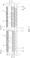
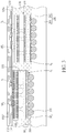
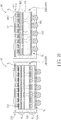
FIG. 1 to FIG. 5 are schematic, cross-sectional diagrams showing an exemplary method for fabricating a semiconductor package with a buried substrate component according to one embodiment of the invention, whereinFIG. 5 shows a cross section of an individual semiconductor package after singulation and de-carrier; -
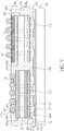
FIG. 6 to FIG. 12 are schematic, cross-sectional diagrams showing an exemplary method for fabricating a semiconductor package with a buried substrate component according to another embodiment of the invention, whereinFIG. 12 shows a cross section of an individual semiconductor package after singulation and de-carrier; -
FIG. 13 to FIG. 17 are schematic, cross-sectional diagrams showing an exemplary method for fabricating a semiconductor package with a buried substrate component according to still another embodiment of the invention, whereinFIG. 17 shows a cross section of an individual semiconductor package after functional die placement; -
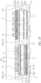
FIG. 18 to FIG. 21 are schematic, cross-sectional diagrams showing an exemplary method for fabricating a semiconductor package with a buried substrate component still according to another embodiment of the invention, whereinFIG. 21 shows a cross section of an individual semiconductor package after functional die placement; and -
FIG. 22 shows a cross section of a semiconductor package according to yet another embodiment of the invention. - In the following detailed description of embodiments of the invention, reference is made to the accompanying drawings, which form a part hereof, and in which is shown by way of illustration specific preferred embodiments in which the disclosure may be practiced.
- These embodiments are described in sufficient detail to enable those skilled in the art to practice them, and it is to be understood that other embodiments may be utilized and that mechanical, chemical, electrical, and procedural changes may be made without departing from the spirit and scope of the present disclosure. The following detailed description is, therefore, not to be taken in a limiting sense, and the scope of embodiments of the present invention is defined only by the appended claims.
- It will be understood that when an element or layer is referred to as being "on", "connected to" or "coupled to" another element or layer, it can be directly on, connected or coupled to the other element or layer or intervening elements or layers may be present. In contrast, when an element is referred to as being "directly on," "directly connected to" or "directly coupled to" another element or layer, there are no intervening elements or layers present. Like numbers refer to like elements throughout. As used herein, the term "and/or" includes any and all combinations of one or more of the associated listed items. The abbreviation "BGA" stands for "ball grid array".
- Packaging of an integrated circuit (IC) chip can involve attaching the IC chip to a substrate (a packaging substrate) which, among other things, provides mechanical support and electrical connections between the chip and other electronic components of a device. Substrate types include, for example, cored substrates, including thin core, thick core (laminate BT (bismaleimide-triazine resin) or FR-4 type fibrous board material), and laminate core, as well as coreless substrates. Cored package substrates, for example, can be built up layer by layer around a central core, with layers of conductive material (usually copper) separated by layers of insulating dielectric, with interlayer connections being formed with through holes or microvias (vias).
- The present disclosure pertains to a chip on RDL on substrate (CRoS) package with fine RDL line/space (e.g., L/S ≤ 2/2 µm; i.e. both of line width and space smaller than or equal to 2µm) integrated on a substrate component. In some embodiments, the substrate component may be a buried, over-molded substrate component. The layer count of the substrate component can be reduced so as to improve the production yield of the substrate component, and the cost of the final package can be reduced. Further, heterogeneous integration with multi-functional devices, passive components or memory can be implemented in one package without preliminary packaging process, e.g., fan-out packaging processes or chip-on-wafer (CoW) processes.
- Please refer to
FIG. 1 to FIG. 5. FIG. 1 to FIG. 5 are schematic, cross-sectional diagrams showing an exemplary method for fabricating a semiconductor package with a buried substrate component according to one embodiment of the invention, whereinFIG. 5 shows a cross section of an individual semiconductor package after singulation and de-carrier. - As shown in
FIG. 1 , acarrier 200 is provided. For example, thecarrier 200 may comprise abase substrate 201 such as a glass substrate, a metal substrate, or a plastic substrate in a panel form or a wafer form, but is not limited thereto. Preferably, thecarrier 200 may comprise aflexible film 202, such as a resin film or an adhesive film, laminated on an upper surface of thebase substrate 201. Preferably, for example, theflexible film 202 may have a thickness of about 200-400µm. - Preferably, a plurality of cored
substrate components 100 is distributed on theflexible film 202. Only two coredsubstrate components substrate component 100a may have a thickness that is smaller than that of the coredsubstrate component 100b due to the process variation. Each of the coredsubstrates 100 has a first surface S1 for electrically coupling with at least one chip or electronic device thereon, a second surface S2 for electrically coupling with an external circuitry such as a printed circuit board or a system board, and a sidewall surface SW extending between the first surface S1 and the second surface S2. Each of the coredsubstrates 100 may comprise acore layer 101, which is composed of a material such as bismaleimide-triazine (BT) resin or the like, and build-up interconnect structure BL1 and BL2 disposed on two opposite surfaces of thecore layer 101, respectively. - Preferably, a plurality of bonding pads BP1 is disposed on the first surface S1 of the cored
substrates 100. Preferably, a plurality of solder ball bonding pads BP2 is disposed on the second surface S2 of the coredsubstrates 100 such that solder balls (or BGA balls) 110 can be mounted on the solder ball bonding pads BP2, respectively, for electrically connecting an external electronic device such as a printed circuit board (not shown). Preferably, at least part of each of thesolder balls 110 sinks and is buried into theflexible film 202. - By controlling the proportion of the
solder balls 110 embedded in theflexible film 202, the first surfaces S1 of the two exemplary coredsubstrate components substrate component 100a and a top surface of theflexible film 202 is greater than a standoff height h2 between the coredsubstrate component 100b and the top surface of theflexible film 202. - As shown in
FIG. 2 , subsequently, the plurality of coredsubstrate components 100 is over-molded by anencapsulant 120 by performing a molding process. For example, the molding process may be compression molding. Preferably, the molding process may be performed by dispensing, but is not limited thereto. Preferably, theencapsulant 120 may comprise an engineered molding compound comprising an epoxy or a resin, but is not limited thereto. Preferably, theencapsulant 120 may surround each of the coredsubstrate components 100 and may fill into thegap 501 between each of the coredsubstrate components 100 and thecarrier 200. Therefore, theencapsulant 120 may cover the second surface S2 and the sidewall surface SW. - After the molding process is completed, a polishing process or a grinding process is performed to remove
excess encapsulant 120 from the first surface S1 of each of the plurality of coredsubstrate components 100, thereby revealing the plurality of flip-chip bonding pads BP1. At this point, the first surface S1 of each of the plurality of coredsubstrate components 100 is approximately flush with anupper surface 120a of theencapsulant 120. - As shown in
FIG. 3 , a re-distribution layer (RDL)structure 130 is then formed directly on the exposed first surface S1 of each of the plurality of coredsubstrate components 100 and on theupper surface 120a of theencapsulant 120. A portion of theRDL structure 130 protrudes beyond the sidewall surface SW of the coredsubstrate component 100. Preferably, the formation of theRDL structure 130 may generally involve the steps of dielectric deposition, metal (e.g., copper) plating, lithography, etching, and/or chemical mechanical polishing (CMP), etc. TheRDL structure 130 may comprisedielectric layers 131, traces 132 in thedielectric layers 131, and re-distributed bonding pads RBP for connecting with an integrated circuit chip or die. - The
dielectric layers 131 may comprise silicon oxide, silicon oxy-nitride, silicon nitride, and/or low-k dielectric layers, but is not limited thereto. It is noteworthy that no copper post or copper pillar is formed between theRDL structure 130 and the plurality of coredsubstrate components 100. Therefore, the cost of the package can be reduced and the performance of the package can be improved. - After the
RDL structure 130 is completed, at least one integrated circuit die is mounted on theRDL structure 130. As shown inFIG. 4 , for example, functional chips or dies 300 may be mounted on theRDL structure 130 through the connectingelements 310 such as metal bumps, solder bumps, solder-capped metal bumps, micro-bumps, C4 bumps, metal pillars, or the like. The functional dies 300 may comprise afirst die 300a and asecond die 300b, for example, for each package. Thefirst die 300a may have a function different from that of thesecond die 300b so as to achieve heterogeneous integration. For example, thefirst die 300a may be a system on a chip (SoC) and thesecond die 300b may be a memory die, but is not limited thereto. It is to be understood that various functional dies such as passive components, antenna components, or the like may also be employed. - Preferably, prior to the placement of the functional chips or dies 300, a circuit test for the
RDL structure 130 may be performed. If theRDL structure 130 of a particular package fails the test, dummy dies may be mounted on the RDL structure that fails the test, instead of the functional dies. - Subsequently, a de-carrier process may be performed to detach the
carrier 200 and a dicing process or a cutting process may be performed to singulate the individual semiconductor package, as shown inFIG. 5 . - Preferably, as shown in
FIG. 5 , thesemiconductor package 10 may be a multi-die package and comprises the coredsubstrate component 100 having acore layer 101, which is composed of a material such as bismaleimide-triazine resin or the like, and build-up interconnect structure BL1 and BL2 disposed on two opposite surfaces of thecore layer 101, respectively. A plurality of plated through holes (PTHs) 101p may be provided in thecore layer 101 for electrically connecting the build-up interconnect structure BL1 with the build-up interconnect structure BL2. For example, preferably, the coredsubstrate component 100 may be a 2-layer, 4-layer, or 6-layer substrate, but is not limited thereto. - The cored
substrate component 100 is surrounded by theencapsulant 120. The coredsubstrate component 100 has the first surface S1 for mounting at least one chip or electronic device thereon, the second surface S2 for electrically coupling with an external circuitry such as a printed circuit board or a system board, and a sidewall surface SW extending between the first surface S1 and the second surface S2. Thesolder balls 110 are mounted on the solder ball bonding pads BP2, respectively, on the second surface S2. Preferably, the sidewall surface SW is covered by theencapsulant 120. Preferably, the second surface S2 is at least partially covered by theencapsulant 120. Preferably, theencapsulant 120 is in direct contact with an upper portion of each of thesolder balls 110. - The first surface S1 of the cored
substrate component 100 is flush with theupper surface 120a of theencapsulant 120. TheRDL structure 130 is formed on the first surface S1 of the coredsubstrate component 100 and on theupper surface 120a of theencapsulant 120. Preferably, theRDL structure 130 comprisesdielectric layers 131, traces 132 in thedielectric layers 131, and re-distributed bonding pads RBP for connecting with an integrated circuit chip or die. Thedielectric layers 131 may comprise silicon oxide, silicon oxy-nitride, silicon nitride, and/or low-k dielectric layers, but is not limited thereto. Preferably, theRDL structure 130 can have a tighter RDL pitch (i.e., L/S ≤ 2/2 µm). - It is noteworthy that no copper post or copper pillar is formed between the
RDL structure 130 and the coredsubstrate component 100 since theRDL structure 130 is fabricated directly on the first surface S1 of thesubstrate component 100 and on theupper surface 120a of theencapsulant 120. Therefore, the cost of the package can be reduced and the performance of the package can be improved. - Preferably, the
semiconductor package 10 further comprises thefirst die 300a and thesecond die 300b mounted on theRDL structure 130 through the connectingelements 310. The connectingelements 310 may comprise metal bumps, solder bumps, solder-capped metal bumps, micro-bumps, C4 bumps, metal pillars, or the like. Preferably, thefirst die 300a may have a function different from that of thesecond die 300b so as to achieve heterogeneous integration. For example, thefirst die 300a may be a system on a chip (SoC) and thesecond die 300b may be a memory die, but is not limited thereto. It is to be understood that various functional dies such as passive components, antenna components, or the like may also be employed. - Please refer to
FIG. 6 to FIG. 12. FIG. 6 to FIG. 12 are schematic, cross-sectional diagrams showing an exemplary "RDL-first" method for fabricating a semiconductor package with a buried substrate component according to another embodiment of the invention, wherein like layers, regions, or elements are designated by like numeral numbers or labels.FIG. 12 shows a cross section of an individual semiconductor package after singulation and de-carrier. - As shown in
FIG. 6 , likewise, acarrier 200 is provided. For example, thecarrier 200 may comprise abase substrate 201 such as a glass substrate, a metal substrate, or a plastic substrate in a panel form or a wafer form, but is not limited thereto. Preferably, thecarrier 200 may comprise aflexible film 202, such as a resin film, a release film, or an adhesive film, laminated on an upper surface of thebase substrate 201. - An
RDL structure 130 is then formed on theflexible film 202. Preferably, the formation of theRDL structure 130 may generally involve the steps of dielectric deposition, metal (e.g., copper) plating, lithography, etching, and/or CMP, etc. TheRDL structure 130 may comprisedielectric layers 131, traces 132 in thedielectric layers 131,bonding pads 134 at an upper surface of theRDL structure 130 for connecting with a substrate component, and re-distributed bonding pads RBP at a lower surface of theRDL structure 130 for connecting with an integrated circuit chip or die. Preferably, thedielectric layers 131 may comprise silicon oxide, silicon oxy-nitride, silicon nitride, and/or low-k dielectric layers, but is not limited thereto. - As shown in
FIG. 7 , a plurality of cored substrate components (or substrate components) 100 is distributed on theRDL structure 130. For the sake of simplicity, only two coredsubstrate components substrate component 100a may have a thickness that is smaller than that of the coredsubstrate component 100b due to the process variation. Each of the coredsubstrates 100 has a first surface S1 for electrically coupling with at least one chip or electronic device thereon, a second surface S2 for electrically coupling with an external circuitry such as a printed circuit board or a system board, and a sidewall surface SW extending between the first surface S1 and the second surface S2. Each of the coredsubstrates 100 may comprise acore layer 101, which is composed of a material such as bismaleimide-triazine (BT) resin or the like, and build-up interconnect structure BL1 and BL2 disposed on two opposite surfaces of thecore layer 101, respectively. - Preferably, the cored
substrate component 100a and the coredsubstrate component 100b are mounted to theRDL structure 130 through a plurality of connectingelements 112 such as solder bumps or solder balls. Preferably, the second surface S2 of the coredsubstrate component 100a may be not leveled with the second surface S2 of the coredsubstrate component 100b. Preferably, a plurality of bonding pads BP1 is disposed on the first surface S1 of the coredsubstrates 100. Preferably, a plurality of solder ball bonding pads BP2 is disposed on the second surface S2 of the coredsubstrates 100. - Subsequently, the cored
substrate components encapsulant 120 by performing a molding process. For example, the molding process may be compression molding. Preferably, the molding process may be performed by dispensing, but is not limited thereto. Preferably, theencapsulant 120 may comprise a molding compound comprising an epoxy or a resin, but is not limited thereto. Preferably, theencapsulant 120 may surround each of the coredsubstrate components 100 and may fill into the gap between each of the coredsubstrate components 100 and thecarrier 200. Preferably, the second surface S2 that faces upwardly at this point is also covered with theencapsulant 120. - As shown in
FIG.8 , viaholes 120v are formed in theencapsulant 120 to expose the solder ball bonding pads BP2 on the second surface S2 of the coredsubstrates 100, respectively. Preferably, the viaholes 120v may be formed by laser drilling processes, but is not limited thereto. - As shown in
FIG. 9 , subsequently, a plurality ofsolder balls 110 can be disposed on the solder ball bonding pads BP2 within the viaholes 120v, respectively, for electrically connecting an external electronic device such as a printed circuit board (not shown). - As shown in
FIG. 10 , anothercarrier 400 is attached to theupper surface 120a of theencapsulant 120. Preferably, thecarrier 400 may comprise abase substrate 401 such as a glass substrate, a metal substrate, or a plastic substrate in a panel form or a wafer form, but is not limited thereto. Preferably, thecarrier 400 may comprise aflexible film 402, such as a resin film or an adhesive film, laminated on an upper surface of thebase substrate 401. - Preferably, the
solder balls 110 may be at least partially buried in theflexible film 402. Subsequently, a de-bonding process may be performed to remove thecarrier 200 from a lower surface of theRDL structure 130. At this point, the re-distributed bonding pads RBP for connecting with an integrated circuit chip or die are revealed. - As shown in
FIG. 11 , thecarrier 400 with the components mounted thereon is flipped 180 degrees. Subsequently, functional chips or dies 300 are mounted on theRDL structure 130 through the connectingelements 310 such as metal bumps, solder bumps, solder-capped metal bumps, micro-bumps, C4 bumps, metal pillars, or the like. The functional dies 300 may comprise afirst die 300a and asecond die 300b, for example, for each package. Thefirst die 300a may have a function different from that of thesecond die 300b so as to achieve heterogeneous integration. For example, thefirst die 300a may be a system on a chip (SoC) and thesecond die 300b may be a memory die, but is not limited thereto. It is to be understood that various functional dies such as passive components, antenna components, or the like may also be employed. - Preferably, prior to the placement of the functional chips or dies 300, a circuit test for the
RDL structure 130 may be performed. If theRDL structure 130 of a particular package fails the test, dummy dies may be mounted on the RDL structure that fails the test, instead of the functional dies. - Subsequently, a de-carrier process may be performed to detach the
carrier 400 and a dicing process or a cutting process may be performed to singulate the individual semiconductor package, as shown inFIG. 12 . - Preferably, as shown in
FIG. 12 , thesemiconductor package 20 may be a multi-die package and comprises the coredsubstrate component 100 having acore layer 101, which is composed of a material such as bismaleimide-triazine resin or the like, and build-up interconnect structure BL1 and BL2 disposed on two opposite surfaces of thecore layer 101, respectively. Likewise, a plurality of plated through holes (PTHs) 101p may be provided in thecore layer 101. For example, preferably, the coredsubstrate component 100 may be a 2-layer, 4-layer, or 6-layer substrate. - The cored
substrate component 100 is surrounded by theencapsulant 120. The coredsubstrate component 100 has the first surface S1 for mounting at least one chip or electronic device thereon, the second surface S2 for electrically coupling with an external circuitry such as a printed circuit board or a system board, and a sidewall surface SW extending between the first surface S1 and the second surface S2. Thesolder balls 110 are mounted on the solder ball bonding pads BP2, respectively, on the second surface S2. Preferably, the sidewall surface SW is covered by theencapsulant 120. Preferably, the second surface S2 is at least partially covered by theencapsulant 120. Preferably, theencapsulant 120 is in direct contact with an upper portion of each of thesolder balls 110. - Preferably, the first surface S1 is at least partially covered by the
encapsulant 120. Therefore, the first surface S1 of the coredsubstrate component 100 is not flush with theupper surface 120a of theencapsulant 120. The connectingelements 112 are disposed on the bonding pads BP1 for further connection, respectively. The connectingelements 112 are surrounded by theencapsulant 120. - The
RDL structure 130 is formed on theupper surface 120a of theencapsulant 120. Preferably, theRDL structure 130 comprisesdielectric layers 131, traces 132 in thedielectric layers 131, and re-distributed bonding pads RBP for connecting with an integrated circuit chip or die. Thedielectric layers 131 may comprise silicon oxide, silicon oxy-nitride, silicon nitride, and/or low-k dielectric layers, but is not limited thereto. Preferably, theRDL structure 130 can have a tighter RDL pitch (i.e., L/S ≤ 2/2 µm). - It is noteworthy that no copper post or copper pillar is formed between the
RDL structure 130 and the coredsubstrate component 100. Therefore, the cost of the package can be reduced and the performance of the package can be improved. Further, since theRDL structure 130 is formed first on thecarrier 200, the production yield of the package can be improved. - Preferably, the
semiconductor package 10 further comprises thefirst die 300a and thesecond die 300b mounted on theRDL structure 130 through the connectingelements 310. The connectingelements 310 may comprise metal bumps, solder bumps, solder-capped metal bumps, micro-bumps, C4 bumps, metal pillars, or the like. Preferably, thefirst die 300a may have a function different from that of thesecond die 300b so as to achieve heterogeneous integration. For example, thefirst die 300a may be a SoC and thesecond die 300b may be a memory die, but is not limited thereto. It is to be understood that various functional dies such as passive components, antenna components, or the like may also be employed. - Please refer to
FIG. 13 to FIG. 17. FIG. 13 to FIG. 17 are schematic, cross-sectional diagrams showing an exemplary "RDL-first" method for fabricating a semiconductor package with a buried substrate component according to another embodiment of the invention, wherein like layers, regions, or elements are designated by like numeral numbers or labels.FIG. 17 shows a cross section of an individual semiconductor package after functional die placement. - As shown in
FIG. 13 , likewise, acarrier 200 is provided. For example, thecarrier 200 may comprise abase substrate 201 such as a glass substrate, a metal substrate, or a plastic substrate in a panel form or a wafer form, but is not limited thereto. Preferably, thecarrier 200 may comprise aflexible film 202, such as a resin film, a release film, or an adhesive film, laminated on an upper surface of thebase substrate 201. - An
RDL structure 130 is then formed on theflexible film 202. Preferably, the formation of theRDL structure 130 may generally involve the steps of dielectric deposition, metal (e.g., copper) plating, lithography, etching, and/or CMP, etc. TheRDL structure 130 may comprisedielectric layers 131, traces 132 in thedielectric layers 131,bonding pads 134 at an upper surface of theRDL structure 130 for connecting with a substrate component, and re-distributed bonding pads RBP at a lower surface of theRDL structure 130 for connecting with an integrated circuit chip or die. Preferably, thedielectric layers 131 may comprise silicon oxide, silicon oxy-nitride, silicon nitride, and/or low-k dielectric layers, but is not limited thereto. Preferably, theRDL structure 130 can have a tighter RDL pitch (i.e., L/S ≤ 2/2 µm). - As shown in
FIG. 14 , a plurality of cored substrate components (or BGA substrate components) 100 is distributed on theRDL structure 130. For the sake of simplicity, only two coredsubstrate components substrate component 100a may have a thickness that is smaller than that of the coredsubstrate component 100b due to the process variation. Each of the coredsubstrates 100 has a first surface S1 for electrically coupling with at least one chip or electronic device thereon and a second surface S2 for electrically coupling with an external circuitry such as a printed circuit board or a system board. Each of the coredsubstrates 100 may comprise acore layer 101, which is composed of a material such as bismaleimide-triazine resin or the like, and build-up interconnect structure BL1 and BL2 disposed on two opposite surfaces of thecore layer 101, respectively. - Preferably, the cored
substrate component 100a and the coredsubstrate component 100b are mounted to theRDL structure 130 through a plurality of connectingelements 112 such as solder bumps or solder balls. Preferably, the second surface S2 of the coredsubstrate component 100a may be not leveled with the second surface S2 of the coredsubstrate component 100b. Preferably, a plurality of bonding pads BP1 is disposed on the first surface S1 of the coredsubstrates 100. Preferably, a plurality of solder ball bonding pads BP2 is disposed on the second surface S2 of the coredsubstrates 100. Solder balls (or BGA balls) 110 are provided on the solder ball bonding pads BP2, respectively. - As shown in
FIG. 15 , subsequently, the coredsubstrate components encapsulant 120 by performing a molding process. For example, the molding process may be compression molding. Preferably, the molding process may be performed by dispensing, but is not limited thereto. Preferably, theencapsulant 120 may comprise a molding compound comprising an epoxy or a resin, but is not limited thereto. Preferably, theencapsulant 120 may surround each of the coredsubstrate components 100 and may fill into the gap between each of the coredsubstrate components 100 and thecarrier 200. Preferably, the second surface S2 that faces upwardly at this point is also covered with theencapsulant 120 and each of thesolder balls 110 is at least partially revealed. - As shown in
FIG. 16 , a de-carrier process may be performed to detach thecarrier 200 and a dicing process or a cutting process may be performed to singulate the individual package 30'. - As shown in
FIG. 17 , subsequently, functional chips or dies 300 are mounted on theRDL structure 130 through the connectingelements 310 such as metal bumps, solder bumps, solder-capped metal bumps, micro-bumps, C4 bumps, metal pillars, or the like, thereby forming thesemiconductor package 30. The functional dies 300 may comprise afirst die 300a and asecond die 300b, for example, for each package. Thefirst die 300a may have a function different from that of thesecond die 300b so as to achieve heterogeneous integration. For example, thefirst die 300a may be a SoC and thesecond die 300b may be a memory die, but is not limited thereto. It is to be understood that various functional dies such as passive components, antenna components, or the like may also be employed. - Preferably, prior to the placement of the functional chips or dies 300, a circuit test for the
RDL structure 130 may be performed. If theRDL structure 130 of a particular package fails the test, dummy dies may be mounted on the RDL structure that fails the test, instead of the functional dies. - Please refer to
FIG. 18 to FIG. 21. FIG. 18 to FIG. 21 are schematic, cross-sectional diagrams showing an exemplary "RDL-first" method for fabricating a semiconductor package with a buried substrate component according to another embodiment of the invention, wherein like layers, regions, or elements are designated by like numeral numbers or labels.FIG. 21 shows a cross section of an individual semiconductor package after functional die placement. - As shown in
FIG. 18 , likewise, acarrier 200 is provided. For example, thecarrier 200 may comprise abase substrate 201 such as a glass substrate, a metal substrate, or a plastic substrate in a panel form or a wafer form, but is not limited thereto. Preferably, thecarrier 200 may comprise aflexible film 202, such as a resin film, a release film, or an adhesive film, laminated on an upper surface of thebase substrate 201. - An
RDL structure 130 is then formed on theflexible film 202. Preferably, the formation of theRDL structure 130 may generally involve the steps of dielectric deposition, metal (e.g., copper) plating, lithography, etching, and/or CMP, etc. TheRDL structure 130 may comprisedielectric layers 131, traces 132 in thedielectric layers 131,bonding pads 134 at an upper surface (or a substrate-side surface) of theRDL structure 130 for connecting with a substrate component, and re-distributed bonding pads RBP at a lower surface (or a chip-side surface) of theRDL structure 130 for connecting with an integrated circuit chip or die. Preferably, thedielectric layers 131 may comprise silicon oxide, silicon oxy-nitride, silicon nitride, and/or low-k dielectric layers, but is not limited thereto. Preferably, theRDL structure 130 can have a tighter RDL pitch (i.e., L/S ≤ 2/2 µm). - As shown in
FIG. 19 , a plurality of cored substrate components (or BGA substrate components) 100 is distributed on theRDL structure 130. For the sake of simplicity, only two coredsubstrate components substrate component 100a may have a thickness that is smaller than that of the coredsubstrate component 100b due to the process variation. Each of the coredsubstrates 100 has a first surface S1 for electrically coupling with at least one chip or electronic device thereon and a second surface S2 for electrically coupling with an external circuitry such as a printed circuit board or a system board. Each of the coredsubstrates 100 may comprise acore layer 101, which is composed of a material such as bismaleimide-triazine resin or the like, and build-up interconnect structure BL1 and BL2 disposed on two opposite surfaces of thecore layer 101, respectively. - Preferably, the cored
substrate component 100a and the coredsubstrate component 100b are mounted to theRDL structure 130 through a plurality of connectingelements 112 such as solder bumps or solder balls. Preferably, the second surface S2 of the coredsubstrate component 100a may be not leveled with the second surface S2 of the coredsubstrate component 100b. Preferably, a plurality of bonding pads BP1 is disposed on the first surface S1 of the coredsubstrates 100. Preferably, a plurality of solder ball bonding pads BP2 is disposed on the second surface S2 of the coredsubstrates 100. Solder balls (or BGA balls) 110 are provided on the solder ball bonding pads BP2, respectively. - Preferably, a
gap 501 is disposed between theRDL structure 130 and the coredsubstrate component 100. Preferably, optionally, thegap 501 between the first surface S1 and theRDL structure 130 may be filled with anunderfill 114 and the connectingelements 112 are surrounded by theunderfill 114. Thegap 501 may have a standoff height h3 that is smaller than 100 µm. Preferably, the standoff height h3 may be smaller than 80 µm. Preferably, theunderfill 114 may comprise a non-conductive paste or a non-conductive film, but is not limited thereto. - As shown in
FIG. 20 , a de-carrier process may be performed to detach thecarrier 200 and a dicing process or a cutting process may be performed to singulate the individual package 40'. Preferably, asidewall surface 130s of the RDL structure is aligned with the sidewall surface SW of the coredsubstrate component 100 along a vertical direction D1. - As shown in
FIG. 21 , subsequently, at least one integrated circuit chip or die such as functional chips or dies 300 are mounted on theRDL structure 130 through the connectingelements 310 such as metal bumps, solder bumps, solder-capped metal bumps, micro-bumps, C4 bumps, metal pillars, or the like, thereby forming thesemiconductor package 40. The functional dies 300 may comprise afirst die 300a and asecond die 300b, for example, for each package. Thefirst die 300a may have a function different from that of thesecond die 300b so as to achieve heterogeneous integration. For example, thefirst die 300a may be a SoC and thesecond die 300b may be a memory die, but is not limited thereto. It is to be understood that various functional dies such as passive components, antenna components, or the like may also be employed. - Preferably, prior to the placement of the functional chips or dies 300, a circuit test for the
RDL structure 130 may be performed. If theRDL structure 130 of a particular package fails the test, dummy dies may be mounted on the RDL structure that fails the test, instead of the functional dies. - In this embodiment, a molding process is omitted. That is, the first surface S1, the second surface S2, and the sidewall surface SW of the cored
substrate component 100 are not covered with an encapsulant. Therefore, the warpage problem of thesemiconductor package 40 can be improved. -
FIG. 22 is a cross-sectional diagram showing a semiconductor package without underfill according to yet another embodiment of the invention, wherein like layers, regions, or elements are designated by like numeral numbers or labels. As shown inFIG. 22 , thesemiconductor package 41 is similar to thesemiconductor package 40 as shown inFIG. 21 . The difference between thesemiconductor package 41 and thesemiconductor package 40 is that thesemiconductor package 41 does not include an underfill between theRDL structure 130 and the coredsubstrate component 100. That is, agap 501 between theRDL structure 130 and the coredsubstrate component 100 is not filled with an underfill and the connectingelements 112 are at least partially exposed. Thegap 501 has a standoff height h3 that is smaller than 100 µm. Preferably, the standoff height h3 is smaller than 80 µm. - Those skilled in the art will readily observe that numerous modifications and alterations of the device and method may be made while retaining the teachings of the invention. Accordingly, the above disclosure should be construed as limited only by the metes and bounds of the appended claims.
Claims (15)
- A semiconductor package (40; 41), comprising:a substrate component (100) comprising a first surface (S1), a second surface (S2) opposite to said first surface (S1), and a sidewall surface (SW) extending between said first surface (S1) and said second surface (S2);a re-distribution layer, in the following also referred to as RDL, structure (130) disposed on said first surface (S1) and electrically connected to said first surface (S1) through first connecting elements (112) comprising solder bumps or balls;a plurality of ball grid array, in the following also referred to as BGA, balls (110) mounted on said second surface (S2) of said substrate component (100); andat least one integrated circuit die (300) mounted on said RDL structure (130) through second connecting elements (310).
- The semiconductor package according to claim 1, wherein said first surface (S1), said second surface (S2), and said sidewall surface (SW) of said substrate component (100) are not covered with an encapsulant.
- The semiconductor package according to claim 1 or 2, wherein a gap (501) is disposed between said RDL structure (130) and said substrate component (100).
- The semiconductor package according to claim 3, wherein said gap (501) has a standoff height h3 that is smaller than 100 µm.
- The semiconductor package according to claim 3 or 4, wherein said gap (501) is filled with an underfill (114) and said first connecting elements (112) are surrounded by the underfill (114).
- The semiconductor package according to claim 5, wherein said underfill (114) comprises a non-conductive paste or a non-conductive film.
- The semiconductor package according to claim 3 or 4, wherein said gap (501) is not filled with an underfill and said first connecting elements (112) are at least partially exposed.
- The semiconductor package according to any one of claims 1 to 7, wherein said RDL structure (130) comprises dielectric layers (131), traces (132) in said dielectric layers (131), bonding pads (134) at a substrate-side surface of said RDL structure (130) for connecting with said substrate component (100), and re-distributed bonding pads (RBP) disposed at a chip-side surface of said RDL structure (130) for connecting with said at least one integrated circuit die (300);
wherein preferably said first connecting elements (112) are directly connected to said bonding pads (134), respectively. - The semiconductor package according to claim 1, wherein a sidewall surface of said RDL structure (130) is aligned with said sidewall surface (SW) of said substrate component (100) along a vertical direction.
- A semiconductor package (10), comprising:a substrate component (100) comprising a first surface (S1), a second surface (S2) opposite to said first surface (S1), and a sidewall surface (SW) extending between said first surface (S1) and said second surface (S2);an encapsulant (120) covering said second surface (S2) and said sidewall surface (SW), wherein said first surface (S1) is flush with an upper surface (120a) of said encapsulant (120);a re-distribution layer, in the following also referred to as RDL, structure (130) disposed directly on said first surface (S1) of said substrate component (100) and on said upper surface (120a) of said encapsulant (120);a plurality of ball grid array, in the following also referred to as BGA, balls (110) mounted on said second surface (S2) of said substrate component (100); andat least one integrated circuit die (300) mounted on said RDL structure (130) through a plurality of connecting elements (310).
- A semiconductor package (20; 30), comprising:a substrate component (100) comprising a first surface (S1), a second surface (S2) opposite to said first surface (S1), and a sidewall surface (SW) extending between said first surface (S1) and said second surface (S2);an encapsulant (120) covering said first surface (S1), said second surface (S2) and said sidewall surface (SW);a re-distribution layer, in the following also referred to as RDL, structure (130) disposed on an upper surface (120a) of said encapsulant (120) and electrically connected to said first surface (S1) through first connecting elements (112) comprising solder bumps or balls;a plurality of ball grid array, in the following also referred to as BGA, balls (110) mounted on said second surface (S2) of said substrate component (100); andat least one integrated circuit die (300) mounted on said RDL structure (130) through a plurality of second connecting elements (310).
- The semiconductor package according to claim 11, wherein said first surface (S1) is not flush with the upper surface (120a) of said encapsulant (120).
- The semiconductor package according to any one of claims 10 to 12, wherein said encapsulant (120) is in direct contact with an upper portion of each of said BGA balls (110).
- The semiconductor package according to any one of claims 10 to 13, wherein said RDL structure (130) comprises dielectric layers (131), traces (132) in said dielectric layers (131), and re-distributed bonding pads (RBP) disposed at a chip-side surface of said RDL structure (130) for connecting with said at least one integrated circuit die (300).
- The semiconductor package according to any one of claims 1 to 14, wherein said RDL structure (130) has an RDL pitch of line/space, in the following also referred to as L/S, ≤ 2/2 µm.
Applications Claiming Priority (2)
| Application Number | Priority Date | Filing Date | Title |
|---|---|---|---|
| US202062959336P | 2020-01-10 | 2020-01-10 | |
| US17/111,456 US20210217707A1 (en) | 2020-01-10 | 2020-12-03 | Semiconductor package having re-distribution layer structure on substrate component |
Publications (3)
| Publication Number | Publication Date |
|---|---|
| EP3848962A2 true EP3848962A2 (en) | 2021-07-14 |
| EP3848962A3 EP3848962A3 (en) | 2021-08-25 |
| EP3848962B1 EP3848962B1 (en) | 2025-06-04 |
Family
ID=73838879
Family Applications (1)
| Application Number | Title | Priority Date | Filing Date |
|---|---|---|---|
| EP20213349.2A Active EP3848962B1 (en) | 2020-01-10 | 2020-12-11 | Semiconductor package having re-distribution layer structure on substrate component |
Country Status (4)
| Country | Link |
|---|---|
| US (1) | US20210217707A1 (en) |
| EP (1) | EP3848962B1 (en) |
| CN (1) | CN113161333A (en) |
| TW (1) | TWI777358B (en) |
Cited By (1)
| Publication number | Priority date | Publication date | Assignee | Title |
|---|---|---|---|---|
| US11410933B2 (en) * | 2020-10-06 | 2022-08-09 | Unimicron Technology Corp. | Package structure and manufacturing method thereof |
Families Citing this family (8)
| Publication number | Priority date | Publication date | Assignee | Title |
|---|---|---|---|---|
| US11810847B2 (en) * | 2021-06-24 | 2023-11-07 | Taiwan Semiconductor Manufacturing Company, Ltd. | Package structure and method of fabricating the same |
| CN115023031A (en) * | 2022-08-08 | 2022-09-06 | 盛合晶微半导体(江阴)有限公司 | High-density integrated substrate structure and manufacturing method |
| US12381141B2 (en) | 2022-08-31 | 2025-08-05 | STATS ChipPAC Pte. Ltd. | Semiconductor device and method of forming hybrid substrate with uniform thickness |
| KR20240034964A (en) * | 2022-09-07 | 2024-03-15 | 삼성전자주식회사 | Semiconductor package |
| US12469791B2 (en) * | 2022-09-28 | 2025-11-11 | STATS ChipPAC Pte. Ltd. | Semiconductor device and method of stacking hybrid substrates with embedded electric components |
| CN118215213A (en) * | 2022-12-16 | 2024-06-18 | 庆鼎精密电子(淮安)有限公司 | Packaging substrate with conducting column and manufacturing method thereof |
| CN118299277A (en) * | 2023-01-05 | 2024-07-05 | 星科金朋私人有限公司 | Semiconductor device and method for manufacturing the same |
| TWI874015B (en) * | 2023-11-30 | 2025-02-21 | 大陸商榮諭科技(成都)有限公司 | Package structure and manufacturing method thereof |
Family Cites Families (30)
| Publication number | Priority date | Publication date | Assignee | Title |
|---|---|---|---|---|
| JP3495300B2 (en) * | 1999-12-10 | 2004-02-09 | Necエレクトロニクス株式会社 | Semiconductor device and manufacturing method thereof |
| JP3677429B2 (en) * | 2000-03-09 | 2005-08-03 | Necエレクトロニクス株式会社 | Method of manufacturing flip chip type semiconductor device |
| EP1205973A1 (en) * | 2000-11-10 | 2002-05-15 | United Test Center Inc. | Low-profile semiconductor device and method for manufacturing the same |
| JP3583396B2 (en) * | 2001-10-31 | 2004-11-04 | 富士通株式会社 | Semiconductor device manufacturing method, thin film multilayer substrate, and manufacturing method thereof |
| US7576435B2 (en) * | 2007-04-27 | 2009-08-18 | Taiwan Semiconductor Manufacturing Company, Ltd. | Low-cost and ultra-fine integrated circuit packaging technique |
| TWI401753B (en) * | 2009-12-31 | 2013-07-11 | 日月光半導體製造股份有限公司 | Method for manufacturing stackable package structure |
| US9601434B2 (en) * | 2010-12-10 | 2017-03-21 | STATS ChipPAC Pte. Ltd. | Semiconductor device and method of forming openings through insulating layer over encapsulant for enhanced adhesion of interconnect structure |
| US9704766B2 (en) * | 2011-04-28 | 2017-07-11 | Taiwan Semiconductor Manufacturing Company, Ltd. | Interposers of 3-dimensional integrated circuit package systems and methods of designing the same |
| KR101904926B1 (en) * | 2012-05-04 | 2018-10-08 | 에스케이하이닉스 주식회사 | Semiconductor package |
| US20140339706A1 (en) * | 2013-05-17 | 2014-11-20 | Nvidia Corporation | Integrated circuit package with an interposer formed from a reusable carrier substrate |
| TWI508157B (en) * | 2013-07-24 | 2015-11-11 | 矽品精密工業股份有限公司 | Semiconductor structure and method of manufacture |
| US9165877B2 (en) * | 2013-10-04 | 2015-10-20 | Mediatek Inc. | Fan-out semiconductor package with copper pillar bumps |
| KR20150091932A (en) * | 2014-02-04 | 2015-08-12 | 앰코 테크놀로지 코리아 주식회사 | Manufacturing method of semiconductor device and semiconductor device thereof |
| US9768090B2 (en) * | 2014-02-14 | 2017-09-19 | Taiwan Semiconductor Manufacturing Company, Ltd. | Substrate design for semiconductor packages and method of forming same |
| US9941207B2 (en) * | 2014-10-24 | 2018-04-10 | STATS ChipPAC Pte. Ltd. | Semiconductor device and method of fabricating 3D package with short cycle time and high yield |
| US9786623B2 (en) * | 2015-03-17 | 2017-10-10 | STATS ChipPAC Pte. Ltd. | Semiconductor device and method of forming PoP semiconductor device with RDL over top package |
| US10043769B2 (en) * | 2015-06-03 | 2018-08-07 | Micron Technology, Inc. | Semiconductor devices including dummy chips |
| US9768145B2 (en) * | 2015-08-31 | 2017-09-19 | Taiwan Semiconductor Manufacturing Company, Ltd. | Methods of forming multi-die package structures including redistribution layers |
| US9875988B2 (en) * | 2015-10-29 | 2018-01-23 | Semtech Corporation | Semiconductor device and method of forming DCALGA package using semiconductor die with micro pillars |
| US9786586B1 (en) * | 2016-08-21 | 2017-10-10 | Micron Technology, Inc. | Semiconductor package and fabrication method thereof |
| US10276525B2 (en) * | 2016-11-28 | 2019-04-30 | Taiwan Semiconductor Manufacturing Co., Ltd. | Package structure and method of fabricating the same |
| US9978731B1 (en) * | 2016-12-28 | 2018-05-22 | Samsung Electro-Mechanics Co., Ltd. | Fan-out semiconductor package module |
| CN108879114A (en) * | 2017-05-16 | 2018-11-23 | 华为技术有限公司 | Integrated antenna packages structure and terminal |
| US11101209B2 (en) * | 2017-09-29 | 2021-08-24 | Taiwan Semiconductor Manufacturing Company, Ltd. | Redistribution structures in semiconductor packages and methods of forming same |
| US10651126B2 (en) * | 2017-12-08 | 2020-05-12 | Applied Materials, Inc. | Methods and apparatus for wafer-level die bridge |
| US10854552B2 (en) * | 2018-06-29 | 2020-12-01 | Taiwan Semiconductor Manufacturing Company, Ltd. | Semiconductor device and method of manufacture |
| US11171090B2 (en) * | 2018-08-30 | 2021-11-09 | Taiwan Semiconductor Manufacturing Company, Ltd. | Semiconductor device and method of manufacture |
| US11421316B2 (en) * | 2018-10-26 | 2022-08-23 | Applied Materials, Inc. | Methods and apparatus for controlling warpage in wafer level packaging processes |
| US11088059B2 (en) * | 2019-06-14 | 2021-08-10 | Taiwan Semiconductor Manufacturing Company, Ltd. | Package structure, RDL structure comprising redistribution layer having ground plates and signal lines and method of forming the same |
| US11282778B2 (en) * | 2019-12-04 | 2022-03-22 | Advanced Semiconductor Engineering, Inc. | Interposer between a conductive substrate and plurality of semiconductor components |
-
2020
- 2020-12-03 US US17/111,456 patent/US20210217707A1/en not_active Abandoned
- 2020-12-11 EP EP20213349.2A patent/EP3848962B1/en active Active
-
2021
- 2021-01-08 TW TW110100762A patent/TWI777358B/en active
- 2021-01-08 CN CN202110025798.5A patent/CN113161333A/en active Pending
Cited By (1)
| Publication number | Priority date | Publication date | Assignee | Title |
|---|---|---|---|---|
| US11410933B2 (en) * | 2020-10-06 | 2022-08-09 | Unimicron Technology Corp. | Package structure and manufacturing method thereof |
Also Published As
| Publication number | Publication date |
|---|---|
| EP3848962A3 (en) | 2021-08-25 |
| CN113161333A (en) | 2021-07-23 |
| TW202127605A (en) | 2021-07-16 |
| EP3848962B1 (en) | 2025-06-04 |
| TWI777358B (en) | 2022-09-11 |
| US20210217707A1 (en) | 2021-07-15 |
Similar Documents
| Publication | Publication Date | Title |
|---|---|---|
| EP3848962B1 (en) | Semiconductor package having re-distribution layer structure on substrate component | |
| KR102637279B1 (en) | Semiconductor device and method of forming an integrated sip module with embedded inductor or package | |
| TWI838944B (en) | Semiconductor device and method of forming embedded die substrate, and system-in-package modules with the same | |
| US7666711B2 (en) | Semiconductor device and method of forming double-sided through vias in saw streets | |
| US7741156B2 (en) | Semiconductor device and method of forming through vias with reflowed conductive material | |
| US8736035B2 (en) | Semiconductor package and method of forming the same | |
| CN111952274B (en) | Electronic package and manufacturing method thereof | |
| US12255182B2 (en) | Electronic package and manufacturing method thereof | |
| US20120018900A1 (en) | Semiconductor Device and Method of Conforming Conductive Vias Between Insulating Layers in Saw Streets | |
| US20250336788A1 (en) | Semiconductor Device and Method of Forming Hybrid Substrate with Uniform Thickness | |
| TW202318932A (en) | Antenna-in-package devices and methods of making | |
| KR20240145436A (en) | Semiconductor device and method of integrating rf antenna interposer with semiconductor package | |
| CN115312490B (en) | Electronic module, manufacturing method thereof and electronic package | |
| US11903145B2 (en) | Wiring board and semiconductor module including the same | |
| CN121487620A (en) | Semiconductor devices and methods for manufacturing fan-out Quilt packages | |
| TW202439585A (en) | Semiconductor device and method of forming an antenna-in-package structure | |
| TW202520461A (en) | Semiconductor device and method of forming fan-out package structure with embedded overhanging backside antenna | |
| KR20250015850A (en) | Semiconductor device and method of forming an antenna-in-package structure | |
| CN119890140A (en) | Semiconductor device and method for manufacturing double-sided bridge die package structure | |
| CN117727719A (en) | Semiconductor devices and methods of stacking hybrid substrates | |
| CN119230522A (en) | Semiconductor device and method for forming an inverted EWLB package having a vertical E-BAR structure |
Legal Events
| Date | Code | Title | Description |
|---|---|---|---|
| PUAI | Public reference made under article 153(3) epc to a published international application that has entered the european phase |
Free format text: ORIGINAL CODE: 0009012 |
|
| STAA | Information on the status of an ep patent application or granted ep patent |
Free format text: STATUS: THE APPLICATION HAS BEEN PUBLISHED |
|
| AK | Designated contracting states |
Kind code of ref document: A2 Designated state(s): AL AT BE BG CH CY CZ DE DK EE ES FI FR GB GR HR HU IE IS IT LI LT LU LV MC MK MT NL NO PL PT RO RS SE SI SK SM TR |
|
| PUAL | Search report despatched |
Free format text: ORIGINAL CODE: 0009013 |
|
| AK | Designated contracting states |
Kind code of ref document: A3 Designated state(s): AL AT BE BG CH CY CZ DE DK EE ES FI FR GB GR HR HU IE IS IT LI LT LU LV MC MK MT NL NO PL PT RO RS SE SI SK SM TR |
|
| RIC1 | Information provided on ipc code assigned before grant |
Ipc: H01L 23/498 20060101AFI20210721BHEP Ipc: H01L 23/538 20060101ALI20210721BHEP |
|
| STAA | Information on the status of an ep patent application or granted ep patent |
Free format text: STATUS: REQUEST FOR EXAMINATION WAS MADE |
|
| 17P | Request for examination filed |
Effective date: 20220217 |
|
| RBV | Designated contracting states (corrected) |
Designated state(s): AL AT BE BG CH CY CZ DE DK EE ES FI FR GB GR HR HU IE IS IT LI LT LU LV MC MK MT NL NO PL PT RO RS SE SI SK SM TR |
|
| P01 | Opt-out of the competence of the unified patent court (upc) registered |
Effective date: 20230607 |
|
| STAA | Information on the status of an ep patent application or granted ep patent |
Free format text: STATUS: EXAMINATION IS IN PROGRESS |
|
| 17Q | First examination report despatched |
Effective date: 20240222 |
|
| GRAP | Despatch of communication of intention to grant a patent |
Free format text: ORIGINAL CODE: EPIDOSNIGR1 |
|
| STAA | Information on the status of an ep patent application or granted ep patent |
Free format text: STATUS: GRANT OF PATENT IS INTENDED |
|
| INTG | Intention to grant announced |
Effective date: 20250109 |
|
| GRAS | Grant fee paid |
Free format text: ORIGINAL CODE: EPIDOSNIGR3 |
|
| GRAA | (expected) grant |
Free format text: ORIGINAL CODE: 0009210 |
|
| STAA | Information on the status of an ep patent application or granted ep patent |
Free format text: STATUS: THE PATENT HAS BEEN GRANTED |
|
| AK | Designated contracting states |
Kind code of ref document: B1 Designated state(s): AL AT BE BG CH CY CZ DE DK EE ES FI FR GB GR HR HU IE IS IT LI LT LU LV MC MK MT NL NO PL PT RO RS SE SI SK SM TR |
|
| REG | Reference to a national code |
Ref country code: GB Ref legal event code: FG4D |
|
| REG | Reference to a national code |
Ref country code: CH Ref legal event code: EP |
|
| REG | Reference to a national code |
Ref country code: DE Ref legal event code: R096 Ref document number: 602020052230 Country of ref document: DE |
|
| REG | Reference to a national code |
Ref country code: IE Ref legal event code: FG4D |
|
| REG | Reference to a national code |
Ref country code: NL Ref legal event code: MP Effective date: 20250604 |
|
| PG25 | Lapsed in a contracting state [announced via postgrant information from national office to epo] |
Ref country code: FI Free format text: LAPSE BECAUSE OF FAILURE TO SUBMIT A TRANSLATION OF THE DESCRIPTION OR TO PAY THE FEE WITHIN THE PRESCRIBED TIME-LIMIT Effective date: 20250604 Ref country code: ES Free format text: LAPSE BECAUSE OF FAILURE TO SUBMIT A TRANSLATION OF THE DESCRIPTION OR TO PAY THE FEE WITHIN THE PRESCRIBED TIME-LIMIT Effective date: 20250604 |
|
| REG | Reference to a national code |
Ref country code: LT Ref legal event code: MG9D |
|
| PG25 | Lapsed in a contracting state [announced via postgrant information from national office to epo] |
Ref country code: GR Free format text: LAPSE BECAUSE OF FAILURE TO SUBMIT A TRANSLATION OF THE DESCRIPTION OR TO PAY THE FEE WITHIN THE PRESCRIBED TIME-LIMIT Effective date: 20250905 Ref country code: NO Free format text: LAPSE BECAUSE OF FAILURE TO SUBMIT A TRANSLATION OF THE DESCRIPTION OR TO PAY THE FEE WITHIN THE PRESCRIBED TIME-LIMIT Effective date: 20250904 |
|
| PG25 | Lapsed in a contracting state [announced via postgrant information from national office to epo] |
Ref country code: PL Free format text: LAPSE BECAUSE OF FAILURE TO SUBMIT A TRANSLATION OF THE DESCRIPTION OR TO PAY THE FEE WITHIN THE PRESCRIBED TIME-LIMIT Effective date: 20250604 |
|
| PG25 | Lapsed in a contracting state [announced via postgrant information from national office to epo] |
Ref country code: BG Free format text: LAPSE BECAUSE OF FAILURE TO SUBMIT A TRANSLATION OF THE DESCRIPTION OR TO PAY THE FEE WITHIN THE PRESCRIBED TIME-LIMIT Effective date: 20250604 |
|
| PG25 | Lapsed in a contracting state [announced via postgrant information from national office to epo] |
Ref country code: HR Free format text: LAPSE BECAUSE OF FAILURE TO SUBMIT A TRANSLATION OF THE DESCRIPTION OR TO PAY THE FEE WITHIN THE PRESCRIBED TIME-LIMIT Effective date: 20250604 |
|
| PGFP | Annual fee paid to national office [announced via postgrant information from national office to epo] |
Ref country code: FR Payment date: 20250930 Year of fee payment: 6 |
|
| PG25 | Lapsed in a contracting state [announced via postgrant information from national office to epo] |
Ref country code: RS Free format text: LAPSE BECAUSE OF FAILURE TO SUBMIT A TRANSLATION OF THE DESCRIPTION OR TO PAY THE FEE WITHIN THE PRESCRIBED TIME-LIMIT Effective date: 20250904 |
|
| PG25 | Lapsed in a contracting state [announced via postgrant information from national office to epo] |
Ref country code: LV Free format text: LAPSE BECAUSE OF FAILURE TO SUBMIT A TRANSLATION OF THE DESCRIPTION OR TO PAY THE FEE WITHIN THE PRESCRIBED TIME-LIMIT Effective date: 20250604 |
|
| PG25 | Lapsed in a contracting state [announced via postgrant information from national office to epo] |
Ref country code: NL Free format text: LAPSE BECAUSE OF FAILURE TO SUBMIT A TRANSLATION OF THE DESCRIPTION OR TO PAY THE FEE WITHIN THE PRESCRIBED TIME-LIMIT Effective date: 20250604 |
|
| REG | Reference to a national code |
Ref country code: DE Ref legal event code: R079 Ref document number: 602020052230 Country of ref document: DE Free format text: PREVIOUS MAIN CLASS: H01L0023498000 Ipc: H10W0070620000 |
|
| PG25 | Lapsed in a contracting state [announced via postgrant information from national office to epo] |
Ref country code: PT Free format text: LAPSE BECAUSE OF FAILURE TO SUBMIT A TRANSLATION OF THE DESCRIPTION OR TO PAY THE FEE WITHIN THE PRESCRIBED TIME-LIMIT Effective date: 20251006 |
|
| REG | Reference to a national code |
Ref country code: AT Ref legal event code: MK05 Ref document number: 1801243 Country of ref document: AT Kind code of ref document: T Effective date: 20250604 |
|
| PG25 | Lapsed in a contracting state [announced via postgrant information from national office to epo] |
Ref country code: IS Free format text: LAPSE BECAUSE OF FAILURE TO SUBMIT A TRANSLATION OF THE DESCRIPTION OR TO PAY THE FEE WITHIN THE PRESCRIBED TIME-LIMIT Effective date: 20251004 |
|
| PGFP | Annual fee paid to national office [announced via postgrant information from national office to epo] |
Ref country code: DE Payment date: 20250930 Year of fee payment: 6 |
|
| PGFP | Annual fee paid to national office [announced via postgrant information from national office to epo] |
Ref country code: GB Payment date: 20251001 Year of fee payment: 6 |
|
| PG25 | Lapsed in a contracting state [announced via postgrant information from national office to epo] |
Ref country code: SM Free format text: LAPSE BECAUSE OF FAILURE TO SUBMIT A TRANSLATION OF THE DESCRIPTION OR TO PAY THE FEE WITHIN THE PRESCRIBED TIME-LIMIT Effective date: 20250604 Ref country code: AT Free format text: LAPSE BECAUSE OF FAILURE TO SUBMIT A TRANSLATION OF THE DESCRIPTION OR TO PAY THE FEE WITHIN THE PRESCRIBED TIME-LIMIT Effective date: 20250604 |
|
| PG25 | Lapsed in a contracting state [announced via postgrant information from national office to epo] |
Ref country code: CZ Free format text: LAPSE BECAUSE OF FAILURE TO SUBMIT A TRANSLATION OF THE DESCRIPTION OR TO PAY THE FEE WITHIN THE PRESCRIBED TIME-LIMIT Effective date: 20250604 |
|
| PG25 | Lapsed in a contracting state [announced via postgrant information from national office to epo] |
Ref country code: EE Free format text: LAPSE BECAUSE OF FAILURE TO SUBMIT A TRANSLATION OF THE DESCRIPTION OR TO PAY THE FEE WITHIN THE PRESCRIBED TIME-LIMIT Effective date: 20250604 |
|
| PG25 | Lapsed in a contracting state [announced via postgrant information from national office to epo] |
Ref country code: RO Free format text: LAPSE BECAUSE OF FAILURE TO SUBMIT A TRANSLATION OF THE DESCRIPTION OR TO PAY THE FEE WITHIN THE PRESCRIBED TIME-LIMIT Effective date: 20250604 Ref country code: SK Free format text: LAPSE BECAUSE OF FAILURE TO SUBMIT A TRANSLATION OF THE DESCRIPTION OR TO PAY THE FEE WITHIN THE PRESCRIBED TIME-LIMIT Effective date: 20250604 |
|
| PG25 | Lapsed in a contracting state [announced via postgrant information from national office to epo] |
Ref country code: IT Free format text: LAPSE BECAUSE OF FAILURE TO SUBMIT A TRANSLATION OF THE DESCRIPTION OR TO PAY THE FEE WITHIN THE PRESCRIBED TIME-LIMIT Effective date: 20250604 |
|
| REG | Reference to a national code |
Ref country code: DE Ref legal event code: R097 Ref document number: 602020052230 Country of ref document: DE |
|
| PLBE | No opposition filed within time limit |
Free format text: ORIGINAL CODE: 0009261 |
|
| STAA | Information on the status of an ep patent application or granted ep patent |
Free format text: STATUS: NO OPPOSITION FILED WITHIN TIME LIMIT |
|
| PG25 | Lapsed in a contracting state [announced via postgrant information from national office to epo] |
Ref country code: DK Free format text: LAPSE BECAUSE OF FAILURE TO SUBMIT A TRANSLATION OF THE DESCRIPTION OR TO PAY THE FEE WITHIN THE PRESCRIBED TIME-LIMIT Effective date: 20250604 |
|
| REG | Reference to a national code |
Ref country code: CH Ref legal event code: L10 Free format text: ST27 STATUS EVENT CODE: U-0-0-L10-L00 (AS PROVIDED BY THE NATIONAL OFFICE) Effective date: 20260416 |
|
| 26N | No opposition filed |
Effective date: 20260305 |