EP3848956A1 - Semiconductor manufacture method and semiconductor manufacture device - Google Patents
Semiconductor manufacture method and semiconductor manufacture device Download PDFInfo
- Publication number
- EP3848956A1 EP3848956A1 EP19857666.2A EP19857666A EP3848956A1 EP 3848956 A1 EP3848956 A1 EP 3848956A1 EP 19857666 A EP19857666 A EP 19857666A EP 3848956 A1 EP3848956 A1 EP 3848956A1
- Authority
- EP
- European Patent Office
- Prior art keywords
- thin film
- metal thin
- laser beam
- laser
- semiconductor
- Prior art date
- Legal status (The legal status is an assumption and is not a legal conclusion. Google has not performed a legal analysis and makes no representation as to the accuracy of the status listed.)
- Pending
Links
Images


Classifications
-
- H—ELECTRICITY
- H10—SEMICONDUCTOR DEVICES; ELECTRIC SOLID-STATE DEVICES NOT OTHERWISE PROVIDED FOR
- H10D—INORGANIC ELECTRIC SEMICONDUCTOR DEVICES
- H10D64/00—Electrodes of devices having potential barriers
- H10D64/01—Manufacture or treatment
- H10D64/011—Manufacture or treatment of electrodes ohmically coupled to a semiconductor
- H10D64/0116—Manufacture or treatment of electrodes ohmically coupled to a semiconductor to Group III-V semiconductors
-
- H—ELECTRICITY
- H10—SEMICONDUCTOR DEVICES; ELECTRIC SOLID-STATE DEVICES NOT OTHERWISE PROVIDED FOR
- H10D—INORGANIC ELECTRIC SEMICONDUCTOR DEVICES
- H10D64/00—Electrodes of devices having potential barriers
- H10D64/60—Electrodes characterised by their materials
- H10D64/62—Electrodes ohmically coupled to a semiconductor
-
- H—ELECTRICITY
- H10—SEMICONDUCTOR DEVICES; ELECTRIC SOLID-STATE DEVICES NOT OTHERWISE PROVIDED FOR
- H10P—GENERIC PROCESSES OR APPARATUS FOR THE MANUFACTURE OR TREATMENT OF DEVICES COVERED BY CLASS H10
- H10P14/00—Formation of materials, e.g. in the shape of layers or pillars
- H10P14/20—Formation of materials, e.g. in the shape of layers or pillars of semiconductor materials
- H10P14/34—Deposited materials, e.g. layers
- H10P14/3402—Deposited materials, e.g. layers characterised by the chemical composition
- H10P14/3414—Deposited materials, e.g. layers characterised by the chemical composition being group IIIA-VIA materials
- H10P14/3416—Nitrides
-
- H—ELECTRICITY
- H10—SEMICONDUCTOR DEVICES; ELECTRIC SOLID-STATE DEVICES NOT OTHERWISE PROVIDED FOR
- H10P—GENERIC PROCESSES OR APPARATUS FOR THE MANUFACTURE OR TREATMENT OF DEVICES COVERED BY CLASS H10
- H10P72/00—Handling or holding of wafers, substrates or devices during manufacture or treatment thereof
- H10P72/04—Apparatus for manufacture or treatment
- H10P72/0431—Apparatus for thermal treatment
- H10P72/0436—Apparatus for thermal treatment mainly by radiation
-
- H—ELECTRICITY
- H10—SEMICONDUCTOR DEVICES; ELECTRIC SOLID-STATE DEVICES NOT OTHERWISE PROVIDED FOR
- H10P—GENERIC PROCESSES OR APPARATUS FOR THE MANUFACTURE OR TREATMENT OF DEVICES COVERED BY CLASS H10
- H10P72/00—Handling or holding of wafers, substrates or devices during manufacture or treatment thereof
- H10P72/06—Apparatus for monitoring, sorting, marking, testing or measuring
- H10P72/0602—Temperature monitoring
-
- H—ELECTRICITY
- H10—SEMICONDUCTOR DEVICES; ELECTRIC SOLID-STATE DEVICES NOT OTHERWISE PROVIDED FOR
- H10P—GENERIC PROCESSES OR APPARATUS FOR THE MANUFACTURE OR TREATMENT OF DEVICES COVERED BY CLASS H10
- H10P72/00—Handling or holding of wafers, substrates or devices during manufacture or treatment thereof
- H10P72/06—Apparatus for monitoring, sorting, marking, testing or measuring
- H10P72/0604—Process monitoring, e.g. flow or thickness monitoring
-
- H—ELECTRICITY
- H10—SEMICONDUCTOR DEVICES; ELECTRIC SOLID-STATE DEVICES NOT OTHERWISE PROVIDED FOR
- H10P—GENERIC PROCESSES OR APPARATUS FOR THE MANUFACTURE OR TREATMENT OF DEVICES COVERED BY CLASS H10
- H10P95/00—Generic processes or apparatus for manufacture or treatments not covered by the other groups of this subclass
- H10P95/90—Thermal treatments, e.g. annealing or sintering
- H10P95/904—Thermal treatments, e.g. annealing or sintering of Group III-V semiconductors
-
- H—ELECTRICITY
- H10—SEMICONDUCTOR DEVICES; ELECTRIC SOLID-STATE DEVICES NOT OTHERWISE PROVIDED FOR
- H10D—INORGANIC ELECTRIC SEMICONDUCTOR DEVICES
- H10D62/00—Semiconductor bodies, or regions thereof, of devices having potential barriers
- H10D62/80—Semiconductor bodies, or regions thereof, of devices having potential barriers characterised by the materials
- H10D62/85—Semiconductor bodies, or regions thereof, of devices having potential barriers characterised by the materials being Group III-V materials, e.g. GaAs
Definitions
- the present invention relates to a semiconductor manufacturing method and a semiconductor manufacturing device.
- a nitride semiconductor represented by AlN, AlGaN, GaN, InGaN, or InN has a wide band gap compared to silicon, and is advanced in application to a high frequency and high output transistor or the like that is operable even under a high temperature environment. With this, a significant reduction in size or high efficiency of equipment is expected.
- an entire substrate is annealed at a predetermined temperature by an annealing device (RTA) to form an ohmic electrode, thereby achieving improvement in ohmic characteristics (for example, see PTL 1).
- RTA annealing device
- the entire substrate is heated in a chamber of the annealing device. For this reason, heating also has an influence on portions other than the ohmic electrode, and there is a problem in that damage to characteristics as a semiconductor, such as high resistance due to the influence of heat, occurs, and electrical characteristics of the wide band gap semiconductor may not be utilized.
- An object of the invention is to efficiently form an ohmic electrode by performing laser annealing locally.
- a semiconductor manufacturing method includes a metal thin film deposition step of depositing a metal thin film on a donor or acceptor-doped nitride semiconductor; and a laser beam irradiation step of irradiating the deposited metal thin film with a laser beam.
- a semiconductor manufacturing device includes a metal thin film deposition unit that deposits a metal thin film on a donor or acceptor-doped nitride semiconductor; and a laser beam irradiation unit that irradiates the metal thin film deposited by the metal thin film deposition unit with a laser beam.
- a metal thin film deposition portion on a substrate, and to suppress an influence of heating on portions other than the ohmic electrode.
- FIG. 1 is a cross-sectional view regarding a semiconductor 10 using a p-type GaN substrate that is an embodiment according to the invention.
- the semiconductor 10 includes a p-type GaN substrate 11, and an electrode 16 made of a metal thin film formed on the p-type GaN substrate 11.
- the semiconductor 10 shown herein is merely an example of a semiconductor using a p-type GaN substrate, and the invention can be applied to a variety of semiconductors using a donor or acceptor-doped nitride semiconductor.
- the p-type GaN substrate 11 As shown in the drawing, a low-temperature (LT) -GaN layer 13 is formed on an upper surface of a substrate 12, and a high-temperature (HT)-GaN layer 14 is formed on an upper surface of the LT-GaN layer 13.
- the p-type GaN substrate 11 has a configuration in which a GaN layer 15 as a nitride semiconductor layer is formed on an upper surface of the HT-GaN layer 14.
- the substrate 12 is not particularly limited and may be made of any crystal as long as a nitride semiconductor layer can be formed on a surface of the substrate 12, and for example, a silicon (Si) substrate, a sapphire substrate, a SiC substrate, and a GaN substrate, and the like can be used.
- a sapphire substrate is exemplified.
- a thickness of the substrate 12 may be a normal thickness (about 100 to 1000 [ ⁇ m]) in a field of semiconductor technology, and is not particularly limited.
- the LT-GaN layer 13 is a buffer layer that is laminated at a lower temperature than the HT-GaN layer 14 and the GaN layer 15 to relax lattice mismatch.
- the buffer layer may be a layer that is generally used in a field of semiconductor technology.
- the HT-GaN layer 14 is laminated and formed at a higher temperature than the LT-GaN layer 13. As the HT-GaN layer 14, a next generation semiconductor material is laminated.
- the GaN layer 15 is made of additive-doped GaN in which any of AlGaN, indium gallium nitride (InGaN) , and aluminum indium gallium nitride (AlInGaN), which is mixed crystal obtained by mixing GaN or GaN and AlN at a predetermined ratio, is doped with an impurity.
- the impurity-doped GaN may be any of p-type GaN where GaN is doped with a p-type impurity and n-type GaN where GaN is doped with an n-type impurity.
- a GaN layer made of p-type GaN is exemplified.
- the GaN layer 15 made of p-type GaN is doped with Mg as an impurity. It is desirable that a doping amount of Mg is within a range equal to or greater than 1.0E+17 and equal to or smaller than 6.0E+19 [cm -3 ] .
- a thickness of the GaN layer 15 is equal to or greater than two times, more desirably, five times, a thickness of a lower electrode 161 of the electrode 16 formed on the GaN layer 15.
- GaN layer 15 consists of n-type GaN
- Si is doped as an impurity.
- a plurality of electrodes 16 are formed at predetermined intervals.
- the electrodes 16 are formed to cover only a portion of one surface of the GaN layer 15, which is a semiconductor layer, without covering the whole of one surface. Then, all electrodes 16 are formed on one surface side of the GaN layer 15 that is a semiconductor layer.
- Such electrodes 16 are formed as ohmic electrodes showing ohmic characteristics.
- a metal material used for such electrodes include gold (Au), titanium (Ti), nickel (Ni), aluminum (Al), vanadium (V), and molybdenum (Mo).
- Au gold
- Ti titanium
- Ni nickel
- Al aluminum
- V vanadium
- Mo molybdenum
- such metal materials may be laminated in a plurality of combinations to form electrodes.
- the electrode 16 consists of a laminated electrode where the lower electrode 161 on the GaN layer 15 side is formed of Ni and an upper electrode 162 laminated on the lower electrode 161 is formed of Au is exemplified.
- the upper electrode 162 is formed of Au, it is possible to protect the lower electrode 161 made of Ni from oxidation or the like.
- the lower electrode 161 has a film thickness equal to or greater than 5 nm and less than 30 nm.
- the thickness is set within the range, whereby heating by laser is effectively performed and satisfactory ohmic contact is realized.
- a semiconductor manufacturing device is a semiconductor manufacturing device suitable for manufacturing the semiconductor 10 described above, and primarily includes an electron beam deposition device 20 (see Fig. 2 ) and a laser machining device 30 (see Fig. 3 ).
- the electron beam deposition device 20 functions as a metal thin film deposition unit that deposits the electrode 16 as a metal thin film on the p-type GaN substrate 11.
- the laser machining device 30 functions as a laser beam irradiation unit that irradiates the electrode 16 made of the metal thin film deposited by the electron beam deposition device 20 with a laser beam.
- Fig. 2 is a schematic configuration diagram of the electron beam deposition device 20.
- the electron beam deposition device 20 includes a stage 21 on which the p-type GaN substrate 11 of the semiconductor 10 is installed, a chamber 22 that stores the stage 21, a cryopump 23 that is connected to an exhaust port 221 of the chamber 22 through a valve 222, a target 24 that is made of a material for forming a metal thin film provided to face the stage 21 at a given interval, a cathode electrode 25 that applies a voltage to a surface opposite to a surface of the target 24 facing the stage 21, and a cathode shield 26 that supports the cathode electrode 25.
- the chamber 22 can cut off outside air to bring an inside into an airtight state. Then, the chamber 22 is provided with a gas introduction port 223 and a valve 224 configured to introduce gas, which generates plasma, in addition to the above-described exhaust port 221 that exhausts inside gas.
- Inert gas for example, Ar gas
- Ar gas is supplied from the gas introduction port 223 into the chamber 22.
- the stage 21 is grounded. Then, a predetermined voltage can be applied to the target 24 facing the stage 21 by the cathode electrode 25. With this, in a case where discharge is generated between the target 24 and the p-type GaN substrate 11 in a state in which inert gas is supplied into the chamber 22, particles made of a target material can be attached to the p-type GaN substrate 11 to be deposited.
- a permanent magnet or an electromagnet may be disposed on a rear surface side (cathode electrode 25) of the target 24 to perform deposition.
- Fig. 3 is a schematic configuration diagram of the laser machining device 30.
- the laser machining device 30 is a laser annealing device that has the electrode 16 of the semiconductor 10 as a machining subject and irradiates the electrode 16 with a laser beam to perform annealing processing.
- the laser machining device 30 includes a laser beam source 31, an attenuator 32, a beam homogenizer 34, a beam scanner 35, a lens 36, a chamber 37, a stage 38, and a photodetector 39.
- the laser beam source 31 outputs a pulsed laser beam in an ultraviolet range.
- the laser beam source 31 can output the pulsed laser beam with a pulse width within a range equal to or greater than 1 [ns] and less than 1000 [ns]. That is, the laser beam source 31 that outputs pulsed laser beam having a desired pulse width within the above-described range is used.
- a Nd:YVO4 laser oscillator that outputs third harmonics having a wavelength of 355 [nm] is used.
- a Nd:YLF laser oscillator or a Nd:YAG laser oscillator may be used.
- the p-type GaN substrate 11 on which the lower electrode 161 is formed can be placed on the stage 38.
- the chamber 37 stores the stage 38 inside and can cut off outside air to bring the inside into an airtight state.
- the chamber 37 is provided with a laser transmission window 371, and can introduce the laser beam from the laser beam source 31 onto the stage 38 inside.
- the lens 36 and the laser transmission window 371 are optical parts that are disposed on a path of the pulsed laser beam scanned by the beam scanner 35.
- the laser transmission window 371 has a structure in which an antireflection film is coated on a surface of a synthetic quartz plate, for example.
- the chamber 37 is provided with an introduction port and an exhaust port (not shown) of oxygen or inert gas (argon, nitrogen, or the like), and can be made into an oxygen atmosphere, air atmosphere, inert atmosphere, or vacuum during laser annealing.
- oxygen or inert gas argon, nitrogen, or the like
- a supply source and an exhaust pump of oxygen or inert gas are omitted in the drawing.
- the attenuator 32 changes an attenuation factor of the pulsed laser beam based on a command from a controller (not shown) of the semiconductor manufacturing device.
- the beam homogenizer 34 homogenizes a beam profile on the surface of the p-type GaN substrate 11.
- the beam scanner 35 scans the pulsed laser beam in a two-dimensional direction based on a scanning command from the controller (not shown) of the semiconductor manufacturing device.
- a galvanoscanner having a pair of movable mirrors can be used.
- the lens 36 consists of, for example, an f ⁇ lens, and realizes a substantially image side telecentric optical system.
- a movement speed of an incidence position of the pulsed laser beam scanned by the beam scanner 35 on the surface of the electrode 16 of the semiconductor 10 is, for example, 200 [mm/s].
- the photodetector 39 is disposed.
- the pulsed laser beam can be made to be incident on the photodetector 39 by controlling the beam scanner 35.
- the photodetector 39 can measure light intensity of the pulsed laser beam, for example, average power or pulse energy.
- the photodetector 39 inputs a measurement result to the controller (not shown), and the controller can confirm the normality of the laser beam source 31, the attenuator 32, and the beam homogenizer 34 based on the measurement result.
- the presence or absence of dirt or deterioration of the lens 36 and the laser transmission window 371 at a place where the pulsed laser beam is transmitted can be confirmed.
- Figs. 4A to 4F are explanatory views showing a manufacturing method of the semiconductor 10 in order.
- the substrate 12 made of a sapphire substrate having a thickness of 0.43 [ ⁇ m] is prepared.
- the LT-GaN layer 13, the HT-GaN layer 14, and the GaN layer 15 are formed on the substrate 12 in order (semiconductor layer forming step).
- vapor phase epitaxy such as metal organic vapor phase epitaxy (MOCVD), hydride vapor phase epitaxy (HVPE), molecular beam epitaxy (MBE), or pulsed laser deposition (PLD) can be used.
- MOCVD metal organic vapor phase epitaxy
- HVPE hydride vapor phase epitaxy
- MBE molecular beam epitaxy
- PLD pulsed laser deposition
- the lower electrode 161 of the electrode 16 made of a metal thin film is formed using the electron beam deposition device 20 (metal thin film deposition step) .
- the GaN layer 15 of the p-type GaN substrate 11 is sufficiently cleaned by organic cleaning, SPM cleaning, acid cleaning, or pure water cleaning, and is sufficiently dried.
- An electrode such as the lower electrode 161 can be formed by deposition with Ni as the target 24 using the electron beam deposition device 20 after application of a photoresist to the upper surface of the GaN layer 15, exposure and development of the photoresist with a photomask in which a desired electrode pattern is formed, removal of the photoresist in a region where an electrode is formed, and cleaning.
- the lower electrode 161 may be formed using a mask member M for laser that is used in laser annealing, instead of a photoresist.
- the mask member M for laser is a flat plate made of a material (stainless steel, nickel alloy, or the like) having a predetermined thickness that bears irradiation of the laser beam. As shown in Fig. 5 , the mask member M for laser has openings M1 corresponding to a forming pattern of an electrode.
- the mask member M for laser is closely attached to an electrode forming surface side of the GaN layer 15 of the p-type GaN substrate 11, and is installed on the stage 21 in the chamber 22 of the electron beam deposition device 20.
- the target 24 made of Ni is mounted to face the stage 21, and the chamber 22 is deaerated and filled with inert gas.
- a voltage is applied to the target 24, and Ni is deposited on the surface of the GaN layer 15 viewed from the mask member M for laser and the openings M1 by electron beam deposition.
- the lower electrode 161 is formed on the electrode forming surface of the GaN layer 15 according to the forming pattern of the electrode.
- laser annealing of the lower electrode 161 by the laser machining device 30 is performed (laser beam irradiation step).
- the p-type GaN substrate 11 on which the lower electrode 161 is formed is installed on the stage 38 in the chamber 37 of the laser machining device 30 along with the mask member M for laser.
- the inside of the chamber 37 is maintained in an air atmosphere state.
- the pulsed laser beam having a pulse width within a range equal to or greater than 1 ns and less than 1000 ns is output from the laser beam source 31.
- the irradiation energy of the laser beam is controlled by the attenuator 32 such that the lower electrode 161 is not melted, and an interface temperature of the lower electrode 161 and the p-type GaN substrate 11 is equal to or lower than 800°C. Furthermore, the interface temperature is set to be at least equal to or higher than 300°.
- the irradiation of the pulsed laser beam is performed in a two-dimensional manner of a main scanning direction and a sub-scanning direction, and the irradiation of the pulsed laser beam is performed such that the whole of the electrode forming surface of the GaN layer 15 of the p-type GaN substrate 11 is within an irradiation range.
- the irradiation of the pulsed laser beam is performed from each opening M1 to each lower electrode 161, and the irradiation of the remaining pulsed laser beam is performed to the mask member M for laser.
- the upper electrode 162 of the electrode 16 made of a metal thin film is formed using the electron beam deposition device 20 again (Au deposition step).
- the upper electrode 162 can also be formed by application of a photoresist to the upper surface of the GaN layer 15, exposure and development of the photoresist with a photomask in which a desired electrode pattern is formed, removal of the photoresist in a region where an electrode is formed, cleaning, and film formation with Au as the target 24 using the electron beam deposition device 20 while removing the mask member M for laser.
- the upper electrode can be formed by film formation with Au as the target 24 using the electron beam deposition device 20 in a state in which the mask member M for laser is mounted.
- the mask member M for laser is detached, and the formation of the electrode 16 on the p-type GaN substrate 11 is completed.
- the lower electrode 161 of the electrode 16 deposited by the laser beam irradiation step is irradiated with the laser beam to perform laser annealing, and thus, it becomes easy to selectively heat only the lower electrode 161 of the p-type GaN substrate 11, and it is possible to achieve satisfactory ohmic junction of the lower electrode 161.
- the semiconductor manufacturing device includes the electron beam deposition device 20 that deposits the metal thin film, and the laser machining device 30 that irradiates the lower electrode 161 made of the metal thin film with the laser beam. For this reason, it is possible to provide a semiconductor manufacturing device that effectively suppresses the influence of heating on the configurations other than the lower electrode 161 while achieving satisfactory ohmic junction of the lower electrode 161.
- the upper electrode 162 made of Au is deposited on the lower electrode 161 after the laser beam irradiation step, and thus, it is possible to effectively perform laser annealing to the lower electrode while preventing the laser beam from being reflected by the upper electrode 162.
- the laser beam by the laser machining device 30 is pulsed laser, and irradiation of the laser beam is performed with a pulse width equal to or greater than 1 ns and less than 1000 ns. With this, it is possible to suppress and control a heat influence in a substrate depth direction.
- the irradiation energy of the laser beam by the laser machining device 30 is set within a range in which the lower electrode 161 is not melted, and the interface temperature of the lower electrode 161 and the GaN layer 15 is equal to or lower than 800°C. With this, it is possible to avoid melting of the lower electrode 161, to suppress a shortage of nitrogen of the p-type GaN substrate 11, and to achieve satisfactory ohmic junction of the lower electrode 161.
- the lower electrode 161 is formed to have a thickness smaller than 30 nm and equal to or greater than 5 nm. As the thickness is set within the range, the lower electrode 161 is effectively heated by laser, and satisfactory ohmic contact is realized.
- the GaN layer 15 of the semiconductor 10 shown in the example is made of Mg-doped p-type GaN, and a doping amount of Mg is 1.6 ⁇ 10 18 [cm -3 ].
- a sapphire substrate was used for the substrate 12, and the GaN layer 15 was formed by a MOCVD device.
- the substrate 12 of the p-type GaN substrate 11 was formed to have a thickness of 430 [ ⁇ m]
- the LT-GaN layer 13 was formed to have a thickness of 0.02 [ ⁇ m]
- the HT-GaN layer 14 was formed to have a thickness of 0.96 [ ⁇ m]
- the GaN layer 15 was formed to have a thickness of 1.0 [ ⁇ m].
- a plurality of lower electrodes 161 were made of Ni, and were formed to have a thickness of 20 [nm] by the electron beam deposition device 20.
- the respective lower electrodes 161 were formed with a width in an arrangement direction of 1 [mm], and the respective lower electrodes 161 were formed at an interval in the arrangement direction of 5 to 500 [ ⁇ m], and specifically, 500 [ ⁇ m].
- Laser annealing was performed on the p-type GaN substrate 11, on which the lower electrodes 161 were formed, by the laser machining device 30.
- the laser beam source 31 output pulsed laser of third harmonics having a wavelength of 355 [nm], and scanned the pulsed laser with a pulse width of 40 [ns], a frequency of 20 [kHz], and a speed of 200 [mm/s] .
- An overlap ratio was 80%/80%. The overlap ratio indicates a proportion of overlap of beam spots of laser output in a pulsed manner in the main scanning direction and the sub-scanning direction.
- the above-described laser annealing was performed at a normal temperature in a state in which the chamber 37 was made into an oxygen atmosphere of a concentration of 20%.
- the upper electrode 162 made of Au was formed to have a thickness of 40 [ ⁇ m] on the lower electrode 161.
- a direct current power supply E was connected to two electrodes 16, and a current flowing in the two electrodes 16 was measured by an ammeter T to measure I-V characteristics of the respective samples.
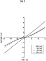
- Fig. 7 is a diagram showing the I-V characteristics of the four samples where laser annealing is performed with 0.5, 1.0, 1.5, and 2.0 [J/cm 2 ].
- the vertical axis indicates a voltage, and the horizontal axis indicates a current.
- the semiconductor 10 may have a configuration in which an electrode is provided on one surface of a GaN layer, and suitable change can be made in other configurations.
- the invention is not limited thereto, and for example, a configuration for irradiation of CW laser may be made.
- the mask member M for laser may not be used, two-dimensional data of an electrode pattern for forming the lower electrode 161 may be prepared in the controller of the semiconductor machining device, and control may be performed such that the beam scanner 35 irradiates only a forming position of the lower electrode 161 with the laser beam.
- a diode sputtering type or magnetron sputtering type sputtering device or an ion beam type sputtering device may be employed.
- a vacuum deposition type, molecular beam deposition type, ion plating type, or ion beam deposition type deposition device may be employed.
- deposition in the embodiment and the claims is a concept including both sputtering by various sputtering devices described above and deposition for attaching a target metal evaporated and vaporized by heating to a substrate.
- the semiconductor manufacturing method and the semiconductor manufacturing device according to the invention have industrial applicability in heating a nitride semiconductor.
Landscapes
- Electrodes Of Semiconductors (AREA)
- Led Devices (AREA)
- Semiconductor Lasers (AREA)
- Health & Medical Sciences (AREA)
- Toxicology (AREA)
Abstract
Description
- The present invention relates to a semiconductor manufacturing method and a semiconductor manufacturing device.
- A nitride semiconductor represented by AlN, AlGaN, GaN, InGaN, or InN has a wide band gap compared to silicon, and is advanced in application to a high frequency and high output transistor or the like that is operable even under a high temperature environment. With this, a significant reduction in size or high efficiency of equipment is expected.
- For such a wide band gap semiconductor, in a manufacturing process, an entire substrate is annealed at a predetermined temperature by an annealing device (RTA) to form an ohmic electrode, thereby achieving improvement in ohmic characteristics (for example, see PTL 1).
- [PTL 1]
Japanese Unexamined Patent Publication No. H10-135515 - However, in the related art, the entire substrate is heated in a chamber of the annealing device. For this reason, heating also has an influence on portions other than the ohmic electrode, and there is a problem in that damage to characteristics as a semiconductor, such as high resistance due to the influence of heat, occurs, and electrical characteristics of the wide band gap semiconductor may not be utilized.
- An object of the invention is to efficiently form an ohmic electrode by performing laser annealing locally.
- A semiconductor manufacturing method according to the invention includes
a metal thin film deposition step of depositing a metal thin film on a donor or acceptor-doped nitride semiconductor; and
a laser beam irradiation step of irradiating the deposited metal thin film with a laser beam. - A semiconductor manufacturing device according to the invention includes
a metal thin film deposition unit that deposits a metal thin film on a donor or acceptor-doped nitride semiconductor; and
a laser beam irradiation unit that irradiates the metal thin film deposited by the metal thin film deposition unit with a laser beam. - According to the invention, it is possible to locally heat a metal thin film deposition portion (ohmic electrode) on a substrate, and to suppress an influence of heating on portions other than the ohmic electrode.
-
-
Fig. 1 is a cross-sectional view regarding a semiconductor using a donor or acceptor-doped nitride semiconductor that is an embodiment according to the invention. -
Fig. 2 is a schematic configuration diagram of an electron beam deposition device of a semiconductor manufacturing device. -
Fig. 3 is a schematic configuration diagram of a laser machining device of the semiconductor manufacturing device. -
Fig. 4A is an explanatory view showing a manufacturing method of a semiconductor. -
Fig. 4B is an explanatory view showing the manufacturing method of the semiconductor subsequent toFig. 4A . -
Fig. 4C is an explanatory view showing the manufacturing method of the semiconductor subsequent toFig. 4B . -
Fig. 4D is an explanatory view showing the manufacturing method of the semiconductor subsequent toFig. 4C . -
Fig. 4E is an explanatory view showing the manufacturing method of the semiconductor subsequent toFig. 4D . -
Fig. 4F is an explanatory view showing the manufacturing method of the semiconductor subsequent toFig. 4E . -
Fig. 5 is a plan view of a mask member for laser. -
Fig. 6 is an explanatory view showing a configuration for measuring an I-V characteristic of a sample where an electrode is subjected to laser annealing. -
Fig. 7 is a diagram showing I-V characteristics of four samples where an electrode is subjected to laser annealing. - Hereinafter, respective embodiments of the invention will be described in detail referring to the drawings. In the embodiment, a semiconductor manufacturing method and a semiconductor manufacturing device for a semiconductor using a donor or acceptor-doped nitride semiconductor will be described.
- Hereinafter, the invention will be specifically described.
Fig. 1 is a cross-sectional view regarding asemiconductor 10 using a p-type GaN substrate that is an embodiment according to the invention. - The
semiconductor 10 includes a p-type GaN substrate 11, and anelectrode 16 made of a metal thin film formed on the p-type GaN substrate 11. - The
semiconductor 10 shown herein is merely an example of a semiconductor using a p-type GaN substrate, and the invention can be applied to a variety of semiconductors using a donor or acceptor-doped nitride semiconductor. - In the p-
type GaN substrate 11, as shown in the drawing, a low-temperature (LT) -GaN layer 13 is formed on an upper surface of asubstrate 12, and a high-temperature (HT)-GaN layer 14 is formed on an upper surface of the LT-GaN layer 13. In addition, the p-type GaN substrate 11 has a configuration in which aGaN layer 15 as a nitride semiconductor layer is formed on an upper surface of the HT-GaN layer 14. - The
substrate 12 is not particularly limited and may be made of any crystal as long as a nitride semiconductor layer can be formed on a surface of thesubstrate 12, and for example, a silicon (Si) substrate, a sapphire substrate, a SiC substrate, and a GaN substrate, and the like can be used. Here, a sapphire substrate is exemplified. A thickness of thesubstrate 12 may be a normal thickness (about 100 to 1000 [µm]) in a field of semiconductor technology, and is not particularly limited. - The LT-
GaN layer 13 is a buffer layer that is laminated at a lower temperature than the HT-GaN layer 14 and theGaN layer 15 to relax lattice mismatch. The buffer layer may be a layer that is generally used in a field of semiconductor technology. - The HT-
GaN layer 14 is laminated and formed at a higher temperature than the LT-GaN layer 13. As the HT-GaN layer 14, a next generation semiconductor material is laminated. - The
GaN layer 15 is made of additive-doped GaN in which any of AlGaN, indium gallium nitride (InGaN) , and aluminum indium gallium nitride (AlInGaN), which is mixed crystal obtained by mixing GaN or GaN and AlN at a predetermined ratio, is doped with an impurity. The impurity-doped GaN may be any of p-type GaN where GaN is doped with a p-type impurity and n-type GaN where GaN is doped with an n-type impurity. Here, a GaN layer made of p-type GaN is exemplified. - The
GaN layer 15 made of p-type GaN is doped with Mg as an impurity. It is desirable that a doping amount of Mg is within a range equal to or greater than 1.0E+17 and equal to or smaller than 6.0E+19 [cm-3] . - Furthermore, a thickness of the
GaN layer 15 is equal to or greater than two times, more desirably, five times, a thickness of alower electrode 161 of theelectrode 16 formed on theGaN layer 15. - Note that, in a case where the
GaN layer 15 consists of n-type GaN, Si is doped as an impurity. - On an upper surface of the
GaN layer 15, a plurality of electrodes 16 (inFig. 1 , only two electrodes are shown) are formed at predetermined intervals. - The
electrodes 16 are formed to cover only a portion of one surface of theGaN layer 15, which is a semiconductor layer, without covering the whole of one surface. Then, allelectrodes 16 are formed on one surface side of theGaN layer 15 that is a semiconductor layer. -
Such electrodes 16 are formed as ohmic electrodes showing ohmic characteristics. Examples of a metal material used for such electrodes include gold (Au), titanium (Ti), nickel (Ni), aluminum (Al), vanadium (V), and molybdenum (Mo). Alternatively, such metal materials may be laminated in a plurality of combinations to form electrodes. - Here, a case where the
electrode 16 consists of a laminated electrode where thelower electrode 161 on theGaN layer 15 side is formed of Ni and anupper electrode 162 laminated on thelower electrode 161 is formed of Au is exemplified. For example, as theupper electrode 162 is formed of Au, it is possible to protect thelower electrode 161 made of Ni from oxidation or the like. - Furthermore, it is desirable that the
lower electrode 161 has a film thickness equal to or greater than 5 nm and less than 30 nm. In regard to thelower electrode 161, while ohmic junction is achieved by laser annealing described below, the thickness is set within the range, whereby heating by laser is effectively performed and satisfactory ohmic contact is realized. - A semiconductor manufacturing device is a semiconductor manufacturing device suitable for manufacturing the
semiconductor 10 described above, and primarily includes an electron beam deposition device 20 (seeFig. 2 ) and a laser machining device 30 (seeFig. 3 ). - The electron
beam deposition device 20 functions as a metal thin film deposition unit that deposits theelectrode 16 as a metal thin film on the p-type GaN substrate 11. - Furthermore, the
laser machining device 30 functions as a laser beam irradiation unit that irradiates theelectrode 16 made of the metal thin film deposited by the electronbeam deposition device 20 with a laser beam. -
Fig. 2 is a schematic configuration diagram of the electronbeam deposition device 20. - As shown in the drawing, the electron
beam deposition device 20 includes astage 21 on which the p-type GaN substrate 11 of thesemiconductor 10 is installed, achamber 22 that stores thestage 21, acryopump 23 that is connected to anexhaust port 221 of thechamber 22 through avalve 222, atarget 24 that is made of a material for forming a metal thin film provided to face thestage 21 at a given interval, acathode electrode 25 that applies a voltage to a surface opposite to a surface of thetarget 24 facing thestage 21, and acathode shield 26 that supports thecathode electrode 25. - The
chamber 22 can cut off outside air to bring an inside into an airtight state. Then, thechamber 22 is provided with agas introduction port 223 and avalve 224 configured to introduce gas, which generates plasma, in addition to the above-describedexhaust port 221 that exhausts inside gas. - Inert gas (for example, Ar gas) is supplied from the
gas introduction port 223 into thechamber 22. - In the
chamber 22, thestage 21 is grounded. Then, a predetermined voltage can be applied to thetarget 24 facing thestage 21 by thecathode electrode 25. With this, in a case where discharge is generated between thetarget 24 and the p-type GaN substrate 11 in a state in which inert gas is supplied into thechamber 22, particles made of a target material can be attached to the p-type GaN substrate 11 to be deposited. - Note that a permanent magnet or an electromagnet may be disposed on a rear surface side (cathode electrode 25) of the
target 24 to perform deposition. -
Fig. 3 is a schematic configuration diagram of thelaser machining device 30. - The
laser machining device 30 is a laser annealing device that has theelectrode 16 of thesemiconductor 10 as a machining subject and irradiates theelectrode 16 with a laser beam to perform annealing processing. - The
laser machining device 30 includes alaser beam source 31, anattenuator 32, abeam homogenizer 34, abeam scanner 35, alens 36, achamber 37, astage 38, and aphotodetector 39. - The
laser beam source 31 outputs a pulsed laser beam in an ultraviolet range. For example, thelaser beam source 31 can output the pulsed laser beam with a pulse width within a range equal to or greater than 1 [ns] and less than 1000 [ns]. That is, thelaser beam source 31 that outputs pulsed laser beam having a desired pulse width within the above-described range is used. - For the
laser beam source 31, for example, a Nd:YVO4 laser oscillator that outputs third harmonics having a wavelength of 355 [nm] is used. In addition, a Nd:YLF laser oscillator or a Nd:YAG laser oscillator may be used. - The p-
type GaN substrate 11 on which thelower electrode 161 is formed can be placed on thestage 38. - The
chamber 37 stores thestage 38 inside and can cut off outside air to bring the inside into an airtight state. - The
chamber 37 is provided with alaser transmission window 371, and can introduce the laser beam from thelaser beam source 31 onto thestage 38 inside. - The
lens 36 and thelaser transmission window 371 are optical parts that are disposed on a path of the pulsed laser beam scanned by thebeam scanner 35. Thelaser transmission window 371 has a structure in which an antireflection film is coated on a surface of a synthetic quartz plate, for example. - Furthermore, the
chamber 37 is provided with an introduction port and an exhaust port (not shown) of oxygen or inert gas (argon, nitrogen, or the like), and can be made into an oxygen atmosphere, air atmosphere, inert atmosphere, or vacuum during laser annealing. Note that a supply source and an exhaust pump of oxygen or inert gas are omitted in the drawing. - The
attenuator 32 changes an attenuation factor of the pulsed laser beam based on a command from a controller (not shown) of the semiconductor manufacturing device. - The
beam homogenizer 34 homogenizes a beam profile on the surface of the p-type GaN substrate 11. - The
beam scanner 35 scans the pulsed laser beam in a two-dimensional direction based on a scanning command from the controller (not shown) of the semiconductor manufacturing device. For thebeam scanner 35, for example, a galvanoscanner having a pair of movable mirrors can be used. - The
lens 36 consists of, for example, an fθ lens, and realizes a substantially image side telecentric optical system. A movement speed of an incidence position of the pulsed laser beam scanned by thebeam scanner 35 on the surface of theelectrode 16 of thesemiconductor 10 is, for example, 200 [mm/s]. - In the
chamber 37, thephotodetector 39 is disposed. The pulsed laser beam can be made to be incident on thephotodetector 39 by controlling thebeam scanner 35. In this state, thephotodetector 39 can measure light intensity of the pulsed laser beam, for example, average power or pulse energy. Thephotodetector 39 inputs a measurement result to the controller (not shown), and the controller can confirm the normality of thelaser beam source 31, theattenuator 32, and thebeam homogenizer 34 based on the measurement result. In addition, the presence or absence of dirt or deterioration of thelens 36 and thelaser transmission window 371 at a place where the pulsed laser beam is transmitted can be confirmed. -
Figs. 4A to 4F are explanatory views showing a manufacturing method of thesemiconductor 10 in order. - As shown in
Fig. 4A , first, thesubstrate 12 made of a sapphire substrate having a thickness of 0.43 [µm] is prepared. - Next, as shown in
Fig. 4B , the LT-GaN layer 13, the HT-GaN layer 14, and theGaN layer 15 are formed on thesubstrate 12 in order (semiconductor layer forming step). In forming the respective layers, vapor phase epitaxy, such as metal organic vapor phase epitaxy (MOCVD), hydride vapor phase epitaxy (HVPE), molecular beam epitaxy (MBE), or pulsed laser deposition (PLD), can be used. - Next, as shown in
Fig. 4C , thelower electrode 161 of theelectrode 16 made of a metal thin film is formed using the electron beam deposition device 20 (metal thin film deposition step) . Note that, prior to forming thelower electrode 161, theGaN layer 15 of the p-type GaN substrate 11 is sufficiently cleaned by organic cleaning, SPM cleaning, acid cleaning, or pure water cleaning, and is sufficiently dried. - An electrode, such as the
lower electrode 161, can be formed by deposition with Ni as thetarget 24 using the electronbeam deposition device 20 after application of a photoresist to the upper surface of theGaN layer 15, exposure and development of the photoresist with a photomask in which a desired electrode pattern is formed, removal of the photoresist in a region where an electrode is formed, and cleaning. - Alternatively, the
lower electrode 161 may be formed using a mask member M for laser that is used in laser annealing, instead of a photoresist. - The mask member M for laser is a flat plate made of a material (stainless steel, nickel alloy, or the like) having a predetermined thickness that bears irradiation of the laser beam. As shown in
Fig. 5 , the mask member M for laser has openings M1 corresponding to a forming pattern of an electrode. - Then, as shown in
Fig. 4C , the mask member M for laser is closely attached to an electrode forming surface side of theGaN layer 15 of the p-type GaN substrate 11, and is installed on thestage 21 in thechamber 22 of the electronbeam deposition device 20. Then, thetarget 24 made of Ni is mounted to face thestage 21, and thechamber 22 is deaerated and filled with inert gas. In addition, a voltage is applied to thetarget 24, and Ni is deposited on the surface of theGaN layer 15 viewed from the mask member M for laser and the openings M1 by electron beam deposition. - With this, the
lower electrode 161 is formed on the electrode forming surface of theGaN layer 15 according to the forming pattern of the electrode. - Next, as shown in
Fig. 4D , laser annealing of thelower electrode 161 by thelaser machining device 30 is performed (laser beam irradiation step). - The p-
type GaN substrate 11 on which thelower electrode 161 is formed is installed on thestage 38 in thechamber 37 of thelaser machining device 30 along with the mask member M for laser. - The inside of the
chamber 37 is maintained in an air atmosphere state. - The pulsed laser beam having a pulse width within a range equal to or greater than 1 ns and less than 1000 ns is output from the
laser beam source 31. - The irradiation energy of the laser beam is controlled by the
attenuator 32 such that thelower electrode 161 is not melted, and an interface temperature of thelower electrode 161 and the p-type GaN substrate 11 is equal to or lower than 800°C. Furthermore, the interface temperature is set to be at least equal to or higher than 300°. - In addition, under the control of the
beam scanner 35, the irradiation of the pulsed laser beam is performed in a two-dimensional manner of a main scanning direction and a sub-scanning direction, and the irradiation of the pulsed laser beam is performed such that the whole of the electrode forming surface of theGaN layer 15 of the p-type GaN substrate 11 is within an irradiation range. With this, the irradiation of the pulsed laser beam is performed from each opening M1 to eachlower electrode 161, and the irradiation of the remaining pulsed laser beam is performed to the mask member M for laser. - With the laser annealing, satisfactory ohmic contact of the
lower electrode 161 with the p-type GaN substrate 11 is realized. - Next, as shown in
Fig. 4E , theupper electrode 162 of theelectrode 16 made of a metal thin film is formed using the electronbeam deposition device 20 again (Au deposition step). - The
upper electrode 162 can also be formed by application of a photoresist to the upper surface of theGaN layer 15, exposure and development of the photoresist with a photomask in which a desired electrode pattern is formed, removal of the photoresist in a region where an electrode is formed, cleaning, and film formation with Au as thetarget 24 using the electronbeam deposition device 20 while removing the mask member M for laser. - Furthermore, instead of the photoresist, the upper electrode can be formed by film formation with Au as the
target 24 using the electronbeam deposition device 20 in a state in which the mask member M for laser is mounted. - Then, as shown in
Fig. 4F , after theupper electrode 162 is formed, the mask member M for laser is detached, and the formation of theelectrode 16 on the p-type GaN substrate 11 is completed. - In the above-described semiconductor manufacturing method, the
lower electrode 161 of theelectrode 16 deposited by the laser beam irradiation step is irradiated with the laser beam to perform laser annealing, and thus, it becomes easy to selectively heat only thelower electrode 161 of the p-type GaN substrate 11, and it is possible to achieve satisfactory ohmic junction of thelower electrode 161. - In addition, it is possible to suppress heating portions other than the
lower electrode 161, and to minimize an influence of heating on the portions other than thelower electrode 161 in the p-type GaN substrate 11. In particular, in a case where configurations other than thelower electrode 161 are already formed on the p-type GaN substrate 11, it is possible to particularly effectively suppress an influence of heating on other configurations. - The semiconductor manufacturing device includes the electron
beam deposition device 20 that deposits the metal thin film, and thelaser machining device 30 that irradiates thelower electrode 161 made of the metal thin film with the laser beam. For this reason, it is possible to provide a semiconductor manufacturing device that effectively suppresses the influence of heating on the configurations other than thelower electrode 161 while achieving satisfactory ohmic junction of thelower electrode 161. - In the semiconductor manufacturing method, the
upper electrode 162 made of Au is deposited on thelower electrode 161 after the laser beam irradiation step, and thus, it is possible to effectively perform laser annealing to the lower electrode while preventing the laser beam from being reflected by theupper electrode 162. - The laser beam by the
laser machining device 30 is pulsed laser, and irradiation of the laser beam is performed with a pulse width equal to or greater than 1 ns and less than 1000 ns. With this, it is possible to suppress and control a heat influence in a substrate depth direction. - The irradiation energy of the laser beam by the
laser machining device 30 is set within a range in which thelower electrode 161 is not melted, and the interface temperature of thelower electrode 161 and theGaN layer 15 is equal to or lower than 800°C. With this, it is possible to avoid melting of thelower electrode 161, to suppress a shortage of nitrogen of the p-type GaN substrate 11, and to achieve satisfactory ohmic junction of thelower electrode 161. - The
lower electrode 161 is formed to have a thickness smaller than 30 nm and equal to or greater than 5 nm. As the thickness is set within the range, thelower electrode 161 is effectively heated by laser, and satisfactory ohmic contact is realized. - An example of the invention will be described.
- The
GaN layer 15 of thesemiconductor 10 shown in the example is made of Mg-doped p-type GaN, and a doping amount of Mg is 1.6×10¹⁸ [cm-3]. A sapphire substrate was used for thesubstrate 12, and theGaN layer 15 was formed by a MOCVD device. - The
substrate 12 of the p-type GaN substrate 11 was formed to have a thickness of 430 [µm], the LT-GaN layer 13 was formed to have a thickness of 0.02 [µm], the HT-GaN layer 14 was formed to have a thickness of 0.96 [µm], and theGaN layer 15 was formed to have a thickness of 1.0 [µm]. - A plurality of
lower electrodes 161 were made of Ni, and were formed to have a thickness of 20 [nm] by the electronbeam deposition device 20. The respectivelower electrodes 161 were formed with a width in an arrangement direction of 1 [mm], and the respectivelower electrodes 161 were formed at an interval in the arrangement direction of 5 to 500 [µm], and specifically, 500 [µm]. - Laser annealing was performed on the p-
type GaN substrate 11, on which thelower electrodes 161 were formed, by thelaser machining device 30. - The
laser beam source 31 output pulsed laser of third harmonics having a wavelength of 355 [nm], and scanned the pulsed laser with a pulse width of 40 [ns], a frequency of 20 [kHz], and a speed of 200 [mm/s] . An overlap ratio was 80%/80%. The overlap ratio indicates a proportion of overlap of beam spots of laser output in a pulsed manner in the main scanning direction and the sub-scanning direction. - The above-described laser annealing was performed at a normal temperature in a state in which the
chamber 37 was made into an oxygen atmosphere of a concentration of 20%. - Under the above-described machining conditions, four samples where laser annealing was performed with laser energy density of 0.5, 1.0, 1.5, and 2.0 [J/cm2], respectively, were prepared.
- In the respective samples, after the laser annealing, the
upper electrode 162 made of Au was formed to have a thickness of 40 [µm] on thelower electrode 161. - In regards to the four samples, as shown in
Fig. 6 , a direct current power supply E was connected to twoelectrodes 16, and a current flowing in the twoelectrodes 16 was measured by an ammeter T to measure I-V characteristics of the respective samples. -
Fig. 7 is a diagram showing the I-V characteristics of the four samples where laser annealing is performed with 0.5, 1.0, 1.5, and 2.0 [J/cm2]. The vertical axis indicates a voltage, and the horizontal axis indicates a current. - As a result, a characteristic of Schottky contact was indicated in three samples where laser annealing was performed with 1.0, 1.5, and 2.0 [J/cm2], and a characteristic of satisfactory ohmic contact was obtained in a sample where laser annealing is performed with 0.5 [J/cm2]. In this sample, it was confirmed by an optical microscope that a surface state after laser irradiation was not melted.
- The embodiment of the invention has been described above. However, the invention is not limited to the above-described embodiment, and suitable changes can be made in the details described in the embodiment without departing from the concept of the invention.
- For example, the
semiconductor 10 may have a configuration in which an electrode is provided on one surface of a GaN layer, and suitable change can be made in other configurations. - Alternatively, in the
laser machining device 30, although a configuration for irradiation of pulsed laser has been made, the invention is not limited thereto, and for example, a configuration for irradiation of CW laser may be made. - Furthermore, in a case where laser annealing is performed on the
lower electrode 161, the mask member M for laser may not be used, two-dimensional data of an electrode pattern for forming thelower electrode 161 may be prepared in the controller of the semiconductor machining device, and control may be performed such that thebeam scanner 35 irradiates only a forming position of thelower electrode 161 with the laser beam. - For the metal thin film deposition unit of the semiconductor machining device, a diode sputtering type or magnetron sputtering type sputtering device or an ion beam type sputtering device may be employed.
- In addition, for the metal thin film deposition unit, a vacuum deposition type, molecular beam deposition type, ion plating type, or ion beam deposition type deposition device may be employed.
- The term "deposition" in the embodiment and the claims is a concept including both sputtering by various sputtering devices described above and deposition for attaching a target metal evaporated and vaporized by heating to a substrate.
- The semiconductor manufacturing method and the semiconductor manufacturing device according to the invention have industrial applicability in heating a nitride semiconductor.
-
- 10 semiconductor
- 11 p-type GaN substrate
- 12 substrate
- 15 GaN layer
- 16 electrode
- 161 lower electrode (metal thin film)
- 162 upper electrode (metal thin film)
- 20 electron beam deposition device(metal thin film deposition unit, Au deposition unit)
- 30 laser machining device(laser beam irradiation unit)
- 31 laser beam source
- 32 attenuator
- 34 beam homogenizer
- 35 beam scanner
- M mask member for laser
Claims (9)
- A semiconductor manufacturing method comprising:a metal thin film deposition step of depositing a metal thin film on a donor or acceptor-doped nitride semiconductor; anda laser beam irradiation step of irradiating the deposited metal thin film with a laser beam.
- The semiconductor manufacturing method according to claim 1, further comprising:
an Au deposition step of depositing Au on the metal thin film after the laser beam irradiation step. - The semiconductor manufacturing method according to claim 1 or 2,
wherein the laser beam is pulsed laser and has a pulse width equal to or greater than 1 ns and less than 1000 ns. - The semiconductor manufacturing method according to any one of claims 1 to 3,
wherein irradiation energy of the laser beam is set such that the metal thin film is not melted, and an interface temperature of the metal thin film and the nitride semiconductor is equal to or lower than 800°C. - The semiconductor manufacturing method according to any one of claims 1 to 4,
wherein the metal thin film has a thickness smaller than 30 nm and equal to or greater than 5 nm. - A semiconductor manufacturing device comprising:a metal thin film deposition unit that deposits a metal thin film on a donor or acceptor-doped nitride semiconductor; anda laser beam irradiation unit that irradiates the metal thin film deposited by the metal thin film deposition unit with a laser beam.
- The semiconductor manufacturing device according to claim 6, further comprising:
an Au deposition unit that deposits Au on the metal thin film. - The semiconductor manufacturing device according to claim 6 or 7,
wherein the laser beam of the laser beam irradiation unit is pulsed laser and has a pulse width equal to or greater than 1 ns and less than 1000 ns. - The semiconductor manufacturing device according to any one of claims 6 to 8,
wherein the laser beam irradiation unit sets irradiation energy of the laser beam such that the metal thin film is not melted, and an interface temperature of the metal thin film and the nitride semiconductor is equal to or lower than 800°C.
Applications Claiming Priority (2)
| Application Number | Priority Date | Filing Date | Title |
|---|---|---|---|
| JP2018168229 | 2018-09-07 | ||
| PCT/JP2019/024914 WO2020049835A1 (en) | 2018-09-07 | 2019-06-24 | Semiconductor manufacture method and semiconductor manufacture device |
Publications (2)
| Publication Number | Publication Date |
|---|---|
| EP3848956A1 true EP3848956A1 (en) | 2021-07-14 |
| EP3848956A4 EP3848956A4 (en) | 2021-11-03 |
Family
ID=69722047
Family Applications (1)
| Application Number | Title | Priority Date | Filing Date |
|---|---|---|---|
| EP19857666.2A Pending EP3848956A4 (en) | 2018-09-07 | 2019-06-24 | SEMICONDUCTOR MANUFACTURING PROCESS AND SEMICONDUCTOR MANUFACTURING DEVICE |
Country Status (5)
| Country | Link |
|---|---|
| US (1) | US20210193470A1 (en) |
| EP (1) | EP3848956A4 (en) |
| JP (2) | JP7374907B2 (en) |
| CN (1) | CN112640046A (en) |
| WO (1) | WO2020049835A1 (en) |
Families Citing this family (2)
| Publication number | Priority date | Publication date | Assignee | Title |
|---|---|---|---|---|
| JP2025171845A (en) * | 2024-05-10 | 2025-11-20 | 住友重機械工業株式会社 | GaAs semiconductor device manufacturing apparatus and GaAs semiconductor device manufacturing method |
| CN121604560A (en) * | 2026-01-26 | 2026-03-03 | 浙江拓感科技有限公司 | Complex pattern electrode alloying method based on ultraviolet pulse laser |
Family Cites Families (20)
| Publication number | Priority date | Publication date | Assignee | Title |
|---|---|---|---|---|
| JPS639118A (en) * | 1986-06-30 | 1988-01-14 | Agency Of Ind Science & Technol | Method for forming ohmic electrodes |
| JPH0784647B2 (en) * | 1988-09-15 | 1995-09-13 | 日本電装株式会社 | Nickel film and sputtering method for forming the same |
| JP2803742B2 (en) * | 1993-04-28 | 1998-09-24 | 日亜化学工業株式会社 | Gallium nitride-based compound semiconductor light emitting device and method for forming electrode thereof |
| JPH08264468A (en) * | 1994-09-12 | 1996-10-11 | Ion Kogaku Kenkyusho:Kk | Method for doping impurities into silicon carbide and method for forming electrode |
| JP3499385B2 (en) | 1996-11-02 | 2004-02-23 | 豊田合成株式会社 | Method for forming group III nitride semiconductor electrode |
| JP2000049114A (en) * | 1998-07-30 | 2000-02-18 | Sony Corp | Electrode, method of forming the same, semiconductor device and method of manufacturing the same |
| JP3523156B2 (en) * | 2000-06-30 | 2004-04-26 | 株式会社東芝 | Semiconductor device and manufacturing method thereof |
| PL354739A1 (en) * | 2002-06-26 | 2003-12-29 | AMMONO Sp.z o.o.AMMONO Sp.z o.o. | Nitride semiconductor laser |
| US20050104072A1 (en) * | 2003-08-14 | 2005-05-19 | Slater David B.Jr. | Localized annealing of metal-silicon carbide ohmic contacts and devices so formed |
| KR100657909B1 (en) * | 2004-11-08 | 2006-12-14 | 삼성전기주식회사 | Electrode Formation Method of Compound Semiconductor Device |
| JP4451811B2 (en) * | 2005-05-09 | 2010-04-14 | ローム株式会社 | Manufacturing method of nitride semiconductor device |
| US8460959B2 (en) * | 2009-11-06 | 2013-06-11 | Ultratech, Inc. | Fast thermal annealing of GaN LEDs |
| JP5608358B2 (en) * | 2009-11-24 | 2014-10-15 | 株式会社豊田中央研究所 | Semiconductor device and manufacturing method thereof |
| JP5187771B2 (en) * | 2009-12-11 | 2013-04-24 | 株式会社日本製鋼所 | Semiconductor substrate manufacturing method and laser annealing apparatus |
| JP2013021175A (en) * | 2011-07-12 | 2013-01-31 | Toshiba Corp | Semiconductor light-emitting element |
| KR101913387B1 (en) * | 2012-03-23 | 2018-10-30 | 삼성전자주식회사 | Selective low-temperature ohmic contact formation method for ⅲ-nitride heterostructure device |
| JP2014078660A (en) * | 2012-10-12 | 2014-05-01 | Sumitomo Electric Ind Ltd | Wide gap semiconductor device and method for manufacturing the same |
| CN104718604B (en) * | 2012-10-23 | 2017-06-30 | 富士电机株式会社 | The manufacture method of semiconductor device |
| WO2018070263A1 (en) * | 2016-10-13 | 2018-04-19 | 三菱電機株式会社 | Method for manufacturing semiconductor device |
| JP6922202B2 (en) * | 2016-12-07 | 2021-08-18 | 富士電機株式会社 | Semiconductor devices and methods for manufacturing semiconductor devices |
-
2019
- 2019-06-24 EP EP19857666.2A patent/EP3848956A4/en active Pending
- 2019-06-24 WO PCT/JP2019/024914 patent/WO2020049835A1/en not_active Ceased
- 2019-06-24 CN CN201980057098.5A patent/CN112640046A/en active Pending
- 2019-06-24 JP JP2020541027A patent/JP7374907B2/en active Active
-
2021
- 2021-03-04 US US17/192,521 patent/US20210193470A1/en not_active Abandoned
-
2023
- 2023-10-24 JP JP2023182231A patent/JP2023178398A/en active Pending
Also Published As
| Publication number | Publication date |
|---|---|
| EP3848956A4 (en) | 2021-11-03 |
| JP2023178398A (en) | 2023-12-14 |
| WO2020049835A1 (en) | 2020-03-12 |
| CN112640046A (en) | 2021-04-09 |
| US20210193470A1 (en) | 2021-06-24 |
| JPWO2020049835A1 (en) | 2021-08-12 |
| JP7374907B2 (en) | 2023-11-07 |
Similar Documents
| Publication | Publication Date | Title |
|---|---|---|
| US7153715B2 (en) | Semiconductor device and method for fabricating the same | |
| CN1993807B (en) | Method for forming p-type semiconductor region and semiconductor element | |
| US8492186B2 (en) | Method for producing group III nitride semiconductor layer, group III nitride semiconductor light-emitting device, and lamp | |
| US8927348B2 (en) | Method of manufacturing group-III nitride semiconductor light-emitting device, and group-III nitride semiconductor light-emitting device, and lamp | |
| JP5073915B2 (en) | Manufacturing method of semiconductor device | |
| TWI424588B (en) | Semiconductor light emitting device manufacturing method | |
| US8198113B2 (en) | Production method for semiconductor light emitting devices | |
| US20180076355A1 (en) | Nitride semiconductor light emitting device | |
| JP2011181762A (en) | Method of manufacturing semiconductor device | |
| JP2023178398A (en) | Semiconductor manufacturing method and semiconductor manufacturing equipment | |
| JP2012188294A (en) | Method for manufacturing semiconductor device | |
| JP5187771B2 (en) | Semiconductor substrate manufacturing method and laser annealing apparatus | |
| JP2008244419A (en) | High electron mobility transistor and manufacturing method thereof | |
| CN113257924B (en) | Schottky diode with high-resistance layer, preparation method of Schottky diode and power diode module | |
| JP4485510B2 (en) | Method for growing semiconductor layer structure | |
| EP4086976B1 (en) | Light emitting element | |
| JP2008300421A (en) | III-V nitride semiconductor manufacturing method and III-V nitride semiconductor | |
| KR100838756B1 (en) | Manufacturing method of nitride semiconductor light emitting device | |
| JPH11274567A (en) | Method for forming electrode of semiconductor element | |
| JP2006210472A (en) | Semiconductor device and manufacturing method thereof | |
| EP3975224B1 (en) | Method for fabrication of recessed electrical elements | |
| JPH11274555A (en) | Semiconductor element | |
| CN118136746A (en) | A laser transfer method for GaN devices based on resonance absorption layer | |
| JP2004266287A (en) | Semiconductor device | |
| Mumthaz Muhammed | Investigation of Emerging Materials for Optoelectronic Devices Based on III-Nitrides |
Legal Events
| Date | Code | Title | Description |
|---|---|---|---|
| STAA | Information on the status of an ep patent application or granted ep patent |
Free format text: STATUS: THE INTERNATIONAL PUBLICATION HAS BEEN MADE |
|
| PUAI | Public reference made under article 153(3) epc to a published international application that has entered the european phase |
Free format text: ORIGINAL CODE: 0009012 |
|
| STAA | Information on the status of an ep patent application or granted ep patent |
Free format text: STATUS: REQUEST FOR EXAMINATION WAS MADE |
|
| 17P | Request for examination filed |
Effective date: 20210219 |
|
| AK | Designated contracting states |
Kind code of ref document: A1 Designated state(s): AL AT BE BG CH CY CZ DE DK EE ES FI FR GB GR HR HU IE IS IT LI LT LU LV MC MK MT NL NO PL PT RO RS SE SI SK SM TR |
|
| STAA | Information on the status of an ep patent application or granted ep patent |
Free format text: STATUS: EXAMINATION IS IN PROGRESS |
|
| A4 | Supplementary search report drawn up and despatched |
Effective date: 20211001 |
|
| RIC1 | Information provided on ipc code assigned before grant |
Ipc: H01L 21/67 20060101ALI20210928BHEP Ipc: H01L 21/285 20060101AFI20210928BHEP |
|
| 17Q | First examination report despatched |
Effective date: 20211014 |
|
| DAV | Request for validation of the european patent (deleted) | ||
| DAX | Request for extension of the european patent (deleted) |